US6882566B2 - Stacked 1T-nMTJ MRAM structure - Google Patents
Stacked 1T-nMTJ MRAM structureDownload PDFInfo
- Publication number
- US6882566B2 US6882566B2US10/895,975US89597504AUS6882566B2US 6882566 B2US6882566 B2US 6882566B2US 89597504 AUS89597504 AUS 89597504AUS 6882566 B2US6882566 B2US 6882566B2
- Authority
- US
- United States
- Prior art keywords
- mram
- line
- forming
- access transistor
- magnetic
- Prior art date
- Legal status (The legal status is an assumption and is not a legal conclusion. Google has not performed a legal analysis and makes no representation as to the accuracy of the status listed.)
- Expired - Lifetime
Links
- 230000005291magnetic effectEffects0.000claimsdescription29
- 230000005294ferromagnetic effectEffects0.000claimsdescription21
- 238000000034methodMethods0.000claimsdescription12
- 239000000758substrateSubstances0.000claimsdescription9
- 230000004888barrier functionEffects0.000claimsdescription3
- 238000004519manufacturing processMethods0.000claims1
- 230000008901benefitEffects0.000abstractdescription8
- 238000005516engineering processMethods0.000abstractdescription4
- 238000012856packingMethods0.000abstractdescription3
- 230000015654memoryEffects0.000description41
- 229910052751metalInorganic materials0.000description14
- 239000002184metalSubstances0.000description14
- 230000002093peripheral effectEffects0.000description12
- 239000004065semiconductorSubstances0.000description11
- 239000000463materialSubstances0.000description8
- 230000006870functionEffects0.000description7
- 239000013598vectorSubstances0.000description4
- XUIMIQQOPSSXEZ-UHFFFAOYSA-NSiliconChemical compound[Si]XUIMIQQOPSSXEZ-UHFFFAOYSA-N0.000description3
- 238000010586diagramMethods0.000description3
- 230000003993interactionEffects0.000description3
- 150000002739metalsChemical class0.000description3
- 150000004767nitridesChemical class0.000description3
- 229910052710siliconInorganic materials0.000description3
- 239000010703siliconSubstances0.000description3
- RYGMFSIKBFXOCR-UHFFFAOYSA-NCopperChemical compound[Cu]RYGMFSIKBFXOCR-UHFFFAOYSA-N0.000description2
- 229910045601alloyInorganic materials0.000description2
- 239000000956alloySubstances0.000description2
- 229910052782aluminiumInorganic materials0.000description2
- XAGFODPZIPBFFR-UHFFFAOYSA-NaluminiumChemical compound[Al]XAGFODPZIPBFFR-UHFFFAOYSA-N0.000description2
- 230000005290antiferromagnetic effectEffects0.000description2
- 239000004020conductorSubstances0.000description2
- 229910052802copperInorganic materials0.000description2
- 239000010949copperSubstances0.000description2
- 230000005415magnetizationEffects0.000description2
- 230000004048modificationEffects0.000description2
- 238000012986modificationMethods0.000description2
- 229910021420polycrystalline siliconInorganic materials0.000description2
- 229920005591polysiliconPolymers0.000description2
- 229910021332silicideInorganic materials0.000description2
- FVBUAEGBCNSCDD-UHFFFAOYSA-Nsilicide(4-)Chemical compound[Si-4]FVBUAEGBCNSCDD-UHFFFAOYSA-N0.000description2
- 230000000638stimulationEffects0.000description2
- WFKWXMTUELFFGS-UHFFFAOYSA-NtungstenChemical compound[W]WFKWXMTUELFFGS-UHFFFAOYSA-N0.000description2
- 229910052721tungstenInorganic materials0.000description2
- 239000010937tungstenSubstances0.000description2
- JBRZTFJDHDCESZ-UHFFFAOYSA-NAsGaChemical compound[As]#[Ga]JBRZTFJDHDCESZ-UHFFFAOYSA-N0.000description1
- 229910001218Gallium arsenideInorganic materials0.000description1
- 241000699670Mus sp.Species0.000description1
- 229910000577Silicon-germaniumInorganic materials0.000description1
- KGWWEXORQXHJJQ-UHFFFAOYSA-N[Fe].[Co].[Ni]Chemical compound[Fe].[Co].[Ni]KGWWEXORQXHJJQ-UHFFFAOYSA-N0.000description1
- LEVVHYCKPQWKOP-UHFFFAOYSA-N[Si].[Ge]Chemical compound[Si].[Ge]LEVVHYCKPQWKOP-UHFFFAOYSA-N0.000description1
- 230000004075alterationEffects0.000description1
- 238000003491arrayMethods0.000description1
- 239000005380borophosphosilicate glassSubstances0.000description1
- 238000001514detection methodMethods0.000description1
- 239000003989dielectric materialSubstances0.000description1
- 230000009977dual effectEffects0.000description1
- 230000008030eliminationEffects0.000description1
- 238000003379elimination reactionMethods0.000description1
- 230000005669field effectEffects0.000description1
- 229910052732germaniumInorganic materials0.000description1
- GNPVGFCGXDBREM-UHFFFAOYSA-Ngermanium atomChemical compound[Ge]GNPVGFCGXDBREM-UHFFFAOYSA-N0.000description1
- 239000012212insulatorSubstances0.000description1
- 230000010354integrationEffects0.000description1
- DALUDRGQOYMVLD-UHFFFAOYSA-Niron manganeseChemical compound[Mn].[Fe]DALUDRGQOYMVLD-UHFFFAOYSA-N0.000description1
- UGKDIUIOSMUOAW-UHFFFAOYSA-Niron nickelChemical compound[Fe].[Ni]UGKDIUIOSMUOAW-UHFFFAOYSA-N0.000description1
- 239000000696magnetic materialSubstances0.000description1
- 229910044991metal oxideInorganic materials0.000description1
- 150000004706metal oxidesChemical class0.000description1
- TWNQGVIAIRXVLR-UHFFFAOYSA-Noxo(oxoalumanyloxy)alumaneChemical compoundO=[Al]O[Al]=OTWNQGVIAIRXVLR-UHFFFAOYSA-N0.000description1
- 238000002161passivationMethods0.000description1
- 230000004044responseEffects0.000description1
- 229910052594sapphireInorganic materials0.000description1
- 239000010980sapphireSubstances0.000description1
- 239000000126substanceSubstances0.000description1
- 238000006467substitution reactionMethods0.000description1
Images


Classifications
- G—PHYSICS
- G11—INFORMATION STORAGE
- G11C—STATIC STORES
- G11C11/00—Digital stores characterised by the use of particular electric or magnetic storage elements; Storage elements therefor
- G11C11/02—Digital stores characterised by the use of particular electric or magnetic storage elements; Storage elements therefor using magnetic elements
- G11C11/16—Digital stores characterised by the use of particular electric or magnetic storage elements; Storage elements therefor using magnetic elements using elements in which the storage effect is based on magnetic spin effect
- B—PERFORMING OPERATIONS; TRANSPORTING
- B82—NANOTECHNOLOGY
- B82Y—SPECIFIC USES OR APPLICATIONS OF NANOSTRUCTURES; MEASUREMENT OR ANALYSIS OF NANOSTRUCTURES; MANUFACTURE OR TREATMENT OF NANOSTRUCTURES
- B82Y10/00—Nanotechnology for information processing, storage or transmission, e.g. quantum computing or single electron logic
- G—PHYSICS
- G11—INFORMATION STORAGE
- G11C—STATIC STORES
- G11C11/00—Digital stores characterised by the use of particular electric or magnetic storage elements; Storage elements therefor
- G11C11/02—Digital stores characterised by the use of particular electric or magnetic storage elements; Storage elements therefor using magnetic elements
- G11C11/14—Digital stores characterised by the use of particular electric or magnetic storage elements; Storage elements therefor using magnetic elements using thin-film elements
- G11C11/15—Digital stores characterised by the use of particular electric or magnetic storage elements; Storage elements therefor using magnetic elements using thin-film elements using multiple magnetic layers
- G—PHYSICS
- G11—INFORMATION STORAGE
- G11C—STATIC STORES
- G11C11/00—Digital stores characterised by the use of particular electric or magnetic storage elements; Storage elements therefor
- G11C11/02—Digital stores characterised by the use of particular electric or magnetic storage elements; Storage elements therefor using magnetic elements
- G11C11/16—Digital stores characterised by the use of particular electric or magnetic storage elements; Storage elements therefor using magnetic elements using elements in which the storage effect is based on magnetic spin effect
- G11C11/165—Auxiliary circuits
- G11C11/1653—Address circuits or decoders
- G11C11/1655—Bit-line or column circuits
- G—PHYSICS
- G11—INFORMATION STORAGE
- G11C—STATIC STORES
- G11C11/00—Digital stores characterised by the use of particular electric or magnetic storage elements; Storage elements therefor
- G11C11/02—Digital stores characterised by the use of particular electric or magnetic storage elements; Storage elements therefor using magnetic elements
- G11C11/16—Digital stores characterised by the use of particular electric or magnetic storage elements; Storage elements therefor using magnetic elements using elements in which the storage effect is based on magnetic spin effect
- G11C11/165—Auxiliary circuits
- G11C11/1659—Cell access
- G—PHYSICS
- G11—INFORMATION STORAGE
- G11C—STATIC STORES
- G11C11/00—Digital stores characterised by the use of particular electric or magnetic storage elements; Storage elements therefor
- G11C11/02—Digital stores characterised by the use of particular electric or magnetic storage elements; Storage elements therefor using magnetic elements
- G11C11/16—Digital stores characterised by the use of particular electric or magnetic storage elements; Storage elements therefor using magnetic elements using elements in which the storage effect is based on magnetic spin effect
- G11C11/165—Auxiliary circuits
- G11C11/1673—Reading or sensing circuits or methods
- H—ELECTRICITY
- H10—SEMICONDUCTOR DEVICES; ELECTRIC SOLID-STATE DEVICES NOT OTHERWISE PROVIDED FOR
- H10B—ELECTRONIC MEMORY DEVICES
- H10B61/00—Magnetic memory devices, e.g. magnetoresistive RAM [MRAM] devices
- H10B61/20—Magnetic memory devices, e.g. magnetoresistive RAM [MRAM] devices comprising components having three or more electrodes, e.g. transistors
- H10B61/22—Magnetic memory devices, e.g. magnetoresistive RAM [MRAM] devices comprising components having three or more electrodes, e.g. transistors of the field-effect transistor [FET] type
Definitions
- the present inventionrelates to magnetoresistive random access memory (MRAM) devices and, more particularly, to read circuitry for such devices.
- MRAMmagnetoresistive random access memory
- MRAMMagnetoresistive random access memory
- a magnetic memory elementhas a structure which includes ferromagnetic layers separated by a non-magnetic barrier layer that forms a tunnel junction. Information can be stored as a digital “1” or a “0” as directions of magnetization vectors in these ferromagnetic layers. Magnetic vectors in one ferromagnetic layer are magnetically fixed or pinned, while the magnetic vectors of the other ferromagnetic layer are not fixed so that the magnetization direction is free to switch between “parallel” and “antiparallel” states relative to the pinned layer.
- the magnetic memory elementIn response to parallel and antiparallel states, the magnetic memory element represents two different resistance states, which are read by the memory circuit as either a “1” or a “0.” It is the detection of these resistance states for the different magnetic orientations that allows the MRAM to read information.
- one architecture usedis the so-called one transistor—one magnetic tunnel junction per cell (“1T-1MTJ”) architecture.
- This structureis based on a single access transistor for controlling read access to a single magnetic memory element.
- Another architectureis the cross-point architecture, where the read operation is performed without using an access transistor to control individual memory cells.
- This type of systemuses row and column lines set to predetermined voltages levels to read a selected cell.
- Each systemhas its advantages and disadvantages.
- the cross-point systemis somewhat slower in reading than the 1T-1MTJ system, as well as being “noisy” during a read operation; however, the cross-point array has the advantage in that it can be easily stacked for higher density.
- a 1T-1MTJ arrayis faster, but necessarily less densely integrated than a cross-point array because additional space is needed to supply the 1-to-1 access transistor to memory cell ratio.
- This inventionprovides an MRAM array read architecture which incorporates certain advantages from both cross-point and 1T-1MTJ architectures.
- the fast read-time and high signal-to-noise ratio of the 1T-1MTJ architecture and the higher packing density of the cross-point architectureare both exploited in the invention by uniquely combining certain characteristics of each.
- a single access transistorcan be used to operate the reading of multiple MRAM cells, which can be stacked vertically above one another in a plurality of MRAM array layers.
- the plurality of standard MRAM cellsessentially share a common sense line, though each MRAM cell can be read individually.
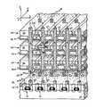
- FIG. 1is a two-dimensional cross-sectional view of a portion of an MRAM array, constructed in accordance with an exemplary embodiment of the invention
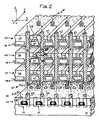
- FIG. 2is a perspective cross-sectional illustration of a portion of an MRAM array, constructed in accordance with the embodiment shown in FIG. 1 ;
- FIG. 3is a block diagram and representational illustration of an MRAM memory cell showing the interaction between the layers of the cell and other circuitry;
- FIG. 4is a block diagram representation of a processor-based system incorporating an MRAM device in accordance with the invention.
- substrateand “wafer” can be used interchangeably in the following description and may include any semiconductor-based structure.
- the structureshould be understood to include silicon, silicon-on insulator (SOI), silicon-on-sapphire (SOS), doped and undoped semiconductors, epitaxial layers of silicon supported by a base semiconductor foundation, and other semiconductor structures.
- SOIsilicon-on insulator
- SOSsilicon-on-sapphire
- doped and undoped semiconductorsepitaxial layers of silicon supported by a base semiconductor foundation, and other semiconductor structures.
- the semiconductorneed not be silicon-based.
- the semiconductorcould be silicon-germanium, germanium, or gallium arsenide.
- metalis intended to include not only elemental metal, but can include metal with other trace metals or in various alloyed combinations with other metals as known in the semiconductor art, as long as such alloy retains the physical and chemical properties of a metal.
- metalis also intended to include conductive oxides of such metals.
- FIG. 1 and FIG. 2illustrate an exemplary embodiment of the invention.
- an access transistor 16is used to control the reading of multiple MRAM cells 38 , which are stacked substantially above one another in a plurality of MRAM array layers 34 that are arranged in the “Z” axis direction.
- each access transistor 16 in a two-dimensional array in the access transistor layer 12can be connected to a substantially vertical stack of a plurality of MRAM cells 38 fabricated substantially over each single access transistor 16 so that the plurality of MRAM cells 38 in this “Z” direction will essentially share a sense line 33 by virtue of a sense line interconnect 32 (explained below).
- This architectureis represented in a two-dimensional cross-section in FIG. 1 and in a three-dimensional cross-section in FIG. 2 .
- the “X,” “Y,” and “Z” axesare shown in both figures.
- FIG. 1shows that the structure of the MRAM device of the invention includes an access transistor layer 12 over a semiconductor substrate 10 .
- the access transistor layer 12includes at least a two-dimensional array (in the “X,Y” plane) of access transistors 16 .
- the access transistors 16are arranged over the substrate 10 along the “X” axis direction.
- what is shownis merely a small cross-section of the MRAM device of the invention for explicative purposes and there can be other access transistors 16 over the substrate in both the “X” and “Y” axis directions.
- the access transistors 16can be typical N-channel MOSFET (metal oxide semiconductor field effect transistor), though the specific structure of the access transistors 16 is not crucial to the invention.
- the transistors 16include source/drain 14 active areas in the substrate 10 .
- the transistor 16includes a gate oxide 18 , and over this there is typically a polysilicon layer 20 with an overlying silicide layer 22 , all topped by a nitride cap 24 .
- the polysilicon layer 20 and silicide layer 22together form a wordline 23 (that continues in the “Y” axis direction).
- the sides of the access transistor 16 wordline 23are insulated and protected by insulating sidewalls 26 , typically made of an oxide or nitride material.
- the wordline 23 of the access transistor 16can be connected to peripheral circuitry 48 (depicted in FIG. 3 ), such as decoding devices and logic circuitry.
- Access transistors 16 for use in this inventioncan be fabricated by any techniques well known to those of skill in the art.
- the access transistor layer 12also includes an insulating dielectric layer 28 over and around the access transistors 16 .
- conductive plugs 30can be fabricated to connect to the source/drain regions 14 of the access transistors 16 .
- the insulating dielectric 28can be any material known in the art, such as an oxide or BPSG, and can be formed according to methods well known in the art.
- the conductive plugs 30similarly can be any material well known in the art, but preferably are tungsten-based, and can be formed by known methods.
- These conductive plugs 30can serve as terminals or connections for electrically connecting the underlying access transistors 16 to the overlying MRAM cells 38 of the MRAM array layers 34 as well as for connection to peripheral circuitry 48 , such as bit lines 31 leading to sense amplifiers 50 used during the reading of the MRAM cells 38 .
- the connections between the access transistors 16 and the MRAM array layers 34 and the bit lines 31are typically formed as metal interconnects 36 , insulated as is known in the art with a dielectric material (not shown).
- the metal interconnects 36 and bit lines 31can be copper, aluminum, or any other metal known as suitable in the art, and can be formed by known methods.
- the bit line 31which is connected to the sense amplifier 50 , is coupled to the access transistors 16 by the metal interconnects 36 and a metal plug 30 .
- MRAM cells 38arranged in “stacked” MRAM array layers 34 are MRAM cells 38 . These cells 38 are arranged in two-dimensional arrays (in the “X,Y” plane) in each layer 34 , where each cell 38 is defined at the intersection of a common line 44 and a sense line 33 , which can be, and generally are, orthogonal to each other. This can also be seen in a three-dimensional perspective in FIG. 2 .
- the sense line 33 for each planar layer 34 for a given vertical stack of memory cells 38are interconnected by a metal interconnect 32 .
- each MRAM cell 38would include, at its most basic configuration, the common line 44 used for both the reading and writing functions, a magnetic bit 42 , a sense line 33 used for the reading function, and a write-only line 40 used for the writing function, which is separated from the sense line 33 by the providing of a dielectric layer 46 .
- the magnetic bit 42includes a free ferromagnetic layer 43 , a tunnel junction layer 45 , and a pinned ferromagnetic layer 41 .
- the free ferromagnetic layer 43is above the pinned ferromagnetic layer 41 , which is adjacent the sense line 33 ; however, it is possible to alter the arrangement of these layers as is known in the art.
- MRAM cells 38 sharing a sense line interconnect 32are in a “column” that is vertical relative to the access transistor 16 .
- other configurationsare possible, such as, for instance, offsetting the cells 38 sharing the sense line interconnect 32 from one another, so long as it is practical to connect a sense line 33 of one cell 38 per layer 34 to the same sense line interconnect 32 .
- the write-only line 40 of the MRAM cell 38can be composed of conductive materials as known in the art; the particular combination of materials making up the write-only line is not a critical element of the invention; however, as an example this line 40 can be copper or aluminum, for instance.
- the write-only line 40is insulated from its surroundings by a dielectric layer 46 , which also insulates other elements of the MRAM cell 38 and the MRAM array layer 34 . Though shown in segments associated with the MRAM cells 38 in FIG. 1 and FIG. 2 , the write-only lines 40 actually are continuous and travel around the sense line interconnects 32 as shown by the dashed arrows in FIG. 1 .
- the pinned ferromagnetic layer 41includes an associated antiferromagnetic layer (not shown), such as iron manganese, which keeps the magnetic orientation of this layer 41 fixed, i.e., “pinned.”
- the magnetic material of the pinned ferromagnetic layer 41can be selected from many various materials or alloys with good magnetic properties, such as nickel iron cobalt or nickel iron, for instance.
- the tunnel junction 45is a region separating the two ferromagnetic layers 41 and 43 and enables the storage of memory as a magnetic orientation (or combination of magnetic vectors) and resulting resistance.
- the tunnel junction 45can be made of many materials, as is known in the art, but the preferred material is aluminum oxide.
- the tunnel junction 45 layershould be thin, smooth and consistent throughout the various MRAM cells 38 , as is known in the art.
- Over the tunnel junction 45is the free ferromagnetic layer 43 , which can be made of the same materials having magnetic properties as the pinned ferromagnetic layer 41 .
- the free ferromagnetic layer 43is free to shift it magnetic orientation for the writing of the MRAM cell 38 and has no associated antiferromagnetic layer.
- the free ferromagnetic layer 43is in electrical contact with a common line 44 (read/write), substantially completing the MRAM cell 38 .
- multiple MRAM array layers 34can be stacked over one another in the “Z” axis direction, thereby increasing the density of the MRAM device.
- a nitride passivation layer(not shown) will typically protect the MRAM device.
- Each MRAM cell 38 of each layer 34has its own sense line 33 , which is connected to the sense line interconnect 32 , which is itself electrically connected to the access transistor 16 , as shown in FIG. 1 and FIG. 2 .
- the sense line 33can be made of any conductive material, but is preferably tungsten-based. As shown in FIG. 1 (and FIG. 2 ) the sense line 33 runs above the write-only line 40 , separated therefrom by the dielectric 46 , and below and in contact with the magnetic bit 45 (specifically, the pinned ferromagnetic layer 41 in the preferred embodiment). In this architecture a single access transistor 16 would be shared by each of the MRAM cells 38 in the “Z” axis direction substantially above the access transistor 16 , as shown in FIG. 2 .
- each access transistor 16is serves a respective cell 38 in each of the MRAM array layers 34 .
- FIG. 2shows additional sense line interconnects 32 extending from the uppermost-shown surface of the MRAM array layers 34 . These sense line interconnects 32 are in contact with other MRAM cells 38 and other access transistors 16 below.
- FIG. 3shows a block-diagram and a representation of an MRAM cell 38 and depicts the interactions of the cell 38 elements with associated circuitry during reading and writing of the cell 38 .
- an MRAM cell 38is addressed by the coinciding stimulation of the common line 44 and a write-only line 40 of that cell 38 by peripheral circuitry, and the actual writing of memory is performed as is known in the art as a function of magnetic orientations of the ferromagnetic layers 41 and 43 , the later of which should be based on the interactions of the magnetic fields of the two lines 44 and 40 caused by the electric currents in these lines 44 and 40 .
- the cell 38is addressed by the coinciding stimulation of a bit line 31 in contact with a sense amplifier 50 , an associated access transistor 16 , and the common line 44 associated with that MRAM cell 38 .
- the cell 38 in the three-dimensional array(as shown in FIG. 2 ) is addressed for reading in the “X” axis direction by an access transistor 16 , in the “Y” axis direction by the bit line 31 (in electrical connection with a peripheral sense amplifier 50 ), and in the “Z” axis direction by the common line 44 of one of the planar layers 34 .
- peripheral circuitry 48will stimulate the wordline 23 , thereby turning on the access transistor 16 .
- the access transistor 16serves to connect a sense amplifier 50 (connected to the source/drain 14 of the transistor 16 by the bit line 31 ) to a sense line interconnect 32 (connected to the other source/drain 14 of the access transistor 16 ) associated with the sense lines 33 of a plurality MRAM cells 38 in the associated “Z” axis direction over that transistor 16 .
- Each of the “columns” of MRAM cells 34can be represented by its association with a sense line interconnect 32 (FIGS. 2 and 3 ).
- the cellis read when the peripheral circuitry 48 stimulates the common line 44 and a sense amplifier 50 connected to that same access transistor 16 senses the memory stored in the cell as a resistance by any method well known in the art.
- each access transistor 16can be in electrical contact with a single respective bit line 31 and that bit line 31 can be in electrical contact with a single respective sense amplifier 50 or, alternatively, multiple bit lines 31 in such an arrangement with associated respective access transistors 16 can be in electrical contact with and share a single sense amplifier 50 .
- a plurality of access transistors 16 having different wordlines 23can share a single bit line 31 and be in electrical contact therewith along its length.
- Each bit line 31 in this type of arrangementcan be in electrical contact with its own respective sense amplifier 50 or, alternatively, multiple such bit lines 31 can be in electrical contact with and share a single sense amplifier 50 .
- the architecture of this inventionprovides for a transistor driver (the access transistor 16 ) for the reading function much closer to both the MRAM cell 38 and the sense amplifier 50 (or other reading device) enabling a faster read function.
- Thisproduces a higher signal-to-noise ratio during the read function than would a conventional cross-point architecture.
- the MRAM three-dimensional arrayessentially consists of an 1T-nMTJ architecture, where n is equal to the number of MRAM array layers 34 or cells 38 in the “Z” axis direction. Accordingly, fewer access transistors 16 are required than is needed in the 1T-1MTJ architecture known in the art.
- FIG. 4illustrates an exemplary processing system 900 which may utilize the memory device 100 of the present invention.
- the processing system 900includes one or more processors 901 coupled to a local bus 904 .
- a memory controller 902 and a primary bus bridge 903are also coupled the local bus 904 .
- the processing system 900may include multiple memory controllers 902 and/or multiple primary bus bridges 903 .
- the memory controller 902 and the primary bus bridge 903may be integrated as a single device 906 .
- the memory controller 902is also coupled to one or more memory buses 907 .
- Each memory busaccepts memory components 908 which include at least one memory device 100 of the present invention.
- the memory components 908may be a memory card or a memory module. Examples of memory modules include single inline memory modules (SIMMs) and dual inline memory modules (DIMMs).
- the memory components 908may include one or more additional devices 909 .
- the additional device 909might be a configuration memory, such as a serial presence detect (SPD) memory.
- the memory controller 902may also be coupled to a cache memory 905 .
- the cache memory 905may be the only cache memory in the processing system.
- processors 901may also include cache memories, which may form a cache hierarchy with cache memory 905 .
- the processing system 900include peripherals or controllers which are bus masters or which support direct memory access (DMA), the memory controller 902 may implement a cache coherency protocol. If the memory controller 902 is coupled to a plurality of memory buses 907 , each memory bus 907 may be operated in parallel, or different address ranges may be mapped to different memory buses 907 .
- DMAdirect memory access
- the primary bus bridge 903is coupled to at least one peripheral bus 910 .
- Various devicessuch as peripherals or additional bus bridges may be coupled to the peripheral bus 910 . These devices may include a storage controller 911 , an miscellaneous I/O device 914 , a secondary bus bridge 915 , a multimedia processor 918 , and an legacy device interface 920 .
- the primary bus bridge 903may also coupled to one or more special purpose high speed ports 922 . In a personal computer, for example, the special purpose port might be the Accelerated Graphics Port (AGP), used to couple a high performance video card to the processing system 900 .
- AGPAccelerated Graphics Port
- the storage controller 911couples one or more storage devices 913 , via a storage bus 912 , to the peripheral bus 910 .
- the storage controller 911may be a SCSI controller and storage devices 913 may be SCSI discs.
- the I/O device 914may be any sort of peripheral.
- the I/O device 914may be an local area network interface, such as an Ethernet card.
- the secondary bus bridgemay be used to interface additional devices via another bus to the processing system.
- the secondary bus bridgemay be an universal serial port (USB) controller used to couple USB devices 917 via to the processing system 900 .
- the multimedia processor 918may be a sound card, a video capture card, or any other type of media interface, which may also be coupled to one additional devices such as speakers 919 .
- the legacy device interface 920is used to couple legacy devices, for example, older styled keyboards and mice, to the processing system 900 .
- FIG. 4illustrates a processing architecture especially suitable for a general purpose computer, such as a personal computer or a workstation, it should be recognized that well known modifications can be made to configure the processing system 900 to become more suitable for use in a variety of applications. For example, many electronic devices which require processing may be implemented using a simpler architecture which relies on a CPU 901 coupled to memory components 908 and/or memory devices 100 .
- These electronic devicesmay include, but are not limited to audio/video processors and recorders, gaming consoles, digital television sets, wired or wireless telephones, navigation devices (including system based on the global positioning system (GPS) and/or inertial navigation), and digital cameras and/or recorders.
- the modificationsmay include, for example, elimination of unnecessary components, addition of specialized devices or circuits, and/or integration of a plurality of devices.
Landscapes
- Engineering & Computer Science (AREA)
- Computer Hardware Design (AREA)
- Chemical & Material Sciences (AREA)
- Nanotechnology (AREA)
- Physics & Mathematics (AREA)
- Mathematical Physics (AREA)
- Theoretical Computer Science (AREA)
- Crystallography & Structural Chemistry (AREA)
- Mram Or Spin Memory Techniques (AREA)
- Hall/Mr Elements (AREA)
- Semiconductor Memories (AREA)
Abstract
Description
This application is a divisional of U.S. patent application Ser. No. 10/146,113, filed May 16, 2002, the entirety of which is hereby incorporated by reference.
The present invention relates to magnetoresistive random access memory (MRAM) devices and, more particularly, to read circuitry for such devices.
Integrated circuit designers have always sought the ideal semiconductor memory: a device that is randomly accessible, can be written or read very quickly, is non-volatile, but indefinitely alterable, and consumes little power. Magnetoresistive random access memory (MRAM) technology has been increasingly viewed as offering all these advantages.
A magnetic memory element has a structure which includes ferromagnetic layers separated by a non-magnetic barrier layer that forms a tunnel junction. Information can be stored as a digital “1” or a “0” as directions of magnetization vectors in these ferromagnetic layers. Magnetic vectors in one ferromagnetic layer are magnetically fixed or pinned, while the magnetic vectors of the other ferromagnetic layer are not fixed so that the magnetization direction is free to switch between “parallel” and “antiparallel” states relative to the pinned layer. In response to parallel and antiparallel states, the magnetic memory element represents two different resistance states, which are read by the memory circuit as either a “1” or a “0.” It is the detection of these resistance states for the different magnetic orientations that allows the MRAM to read information.
There are different array architectures that are used within MRAM technology to read memory cells. For instance, one architecture used is the so-called one transistor—one magnetic tunnel junction per cell (“1T-1MTJ”) architecture. This structure is based on a single access transistor for controlling read access to a single magnetic memory element. Another architecture is the cross-point architecture, where the read operation is performed without using an access transistor to control individual memory cells. This type of system uses row and column lines set to predetermined voltages levels to read a selected cell. Each system has its advantages and disadvantages. The cross-point system is somewhat slower in reading than the 1T-1MTJ system, as well as being “noisy” during a read operation; however, the cross-point array has the advantage in that it can be easily stacked for higher density. Additionally, a 1T-1MTJ array is faster, but necessarily less densely integrated than a cross-point array because additional space is needed to supply the 1-to-1 access transistor to memory cell ratio.
It would be desirable to have an MRAM read architecture that could utilize advantages from both the 1T-1MTJ and cross-point architectures while minimizing the disadvantages of each.
This invention provides an MRAM array read architecture which incorporates certain advantages from both cross-point and 1T-1MTJ architectures. The fast read-time and high signal-to-noise ratio of the 1T-1MTJ architecture and the higher packing density of the cross-point architecture are both exploited in the invention by uniquely combining certain characteristics of each. A single access transistor can be used to operate the reading of multiple MRAM cells, which can be stacked vertically above one another in a plurality of MRAM array layers. In this architecture, the plurality of standard MRAM cells essentially share a common sense line, though each MRAM cell can be read individually.
In the following detailed description, reference is made to various specific embodiments in which the invention may be practiced. These embodiments are described with sufficient detail to enable those skilled in the art to practice the invention, and it is to be understood that other embodiments may be employed, and that structural and electrical changes may be made without departing from the spirit or scope of the present invention.
The terms “substrate” and “wafer” can be used interchangeably in the following description and may include any semiconductor-based structure. The structure should be understood to include silicon, silicon-on insulator (SOI), silicon-on-sapphire (SOS), doped and undoped semiconductors, epitaxial layers of silicon supported by a base semiconductor foundation, and other semiconductor structures. The semiconductor need not be silicon-based. The semiconductor could be silicon-germanium, germanium, or gallium arsenide. When reference is made to the substrate in the following description, previous process steps may have been utilized to form regions or junctions in or over the base semiconductor or foundation.
The term “metal” is intended to include not only elemental metal, but can include metal with other trace metals or in various alloyed combinations with other metals as known in the semiconductor art, as long as such alloy retains the physical and chemical properties of a metal. The term “metal” is also intended to include conductive oxides of such metals.
This invention relates to MRAM technology and new variations on MRAM array architecture to incorporate certain advantages from both cross-point and 1T-1MTJ architectures. The fast read-time and high signal-to-noise ratio of the 1T-1MTJ architecture and the higher packing density of the cross-point architecture are both exploited by combining certain characteristics of each layout. FIG.1 andFIG. 2 illustrate an exemplary embodiment of the invention. In the invention anaccess transistor 16 is used to control the reading ofmultiple MRAM cells 38, which are stacked substantially above one another in a plurality ofMRAM array layers 34 that are arranged in the “Z” axis direction. In this architecture, eachaccess transistor 16 in a two-dimensional array in theaccess transistor layer 12 can be connected to a substantially vertical stack of a plurality ofMRAM cells 38 fabricated substantially over eachsingle access transistor 16 so that the plurality ofMRAM cells 38 in this “Z” direction will essentially share asense line 33 by virtue of a sense line interconnect32 (explained below). This architecture is represented in a two-dimensional cross-section in FIG.1 and in a three-dimensional cross-section in FIG.2. The “X,” “Y,” and “Z” axes are shown in both figures.
Now referring to the figures, where like reference numbers designate like elements,FIG. 1 shows that the structure of the MRAM device of the invention includes anaccess transistor layer 12 over asemiconductor substrate 10. Theaccess transistor layer 12 includes at least a two-dimensional array (in the “X,Y” plane) ofaccess transistors 16. As shown inFIG. 1 , theaccess transistors 16 are arranged over thesubstrate 10 along the “X” axis direction. However, what is shown is merely a small cross-section of the MRAM device of the invention for explicative purposes and there can beother access transistors 16 over the substrate in both the “X” and “Y” axis directions.
As shown inFIG. 1 , theaccess transistors 16 can be typical N-channel MOSFET (metal oxide semiconductor field effect transistor), though the specific structure of theaccess transistors 16 is not crucial to the invention. Thetransistors 16 include source/drain 14 active areas in thesubstrate 10. Over thesubstrate 10, thetransistor 16 includes agate oxide 18, and over this there is typically a polysilicon layer20 with anoverlying silicide layer 22, all topped by anitride cap 24. The polysilicon layer20 andsilicide layer 22 together form a wordline23 (that continues in the “Y” axis direction). The sides of theaccess transistor 16wordline 23 are insulated and protected by insulatingsidewalls 26, typically made of an oxide or nitride material. Thewordline 23 of theaccess transistor 16 can be connected to peripheral circuitry48 (depicted in FIG.3), such as decoding devices and logic circuitry.Access transistors 16 for use in this invention can be fabricated by any techniques well known to those of skill in the art.
Still referring toFIG. 1 , theaccess transistor layer 12 also includes an insulatingdielectric layer 28 over and around theaccess transistors 16. Through this insulatingdielectric layer 28conductive plugs 30 can be fabricated to connect to the source/drain regions 14 of theaccess transistors 16. The insulating dielectric28 can be any material known in the art, such as an oxide or BPSG, and can be formed according to methods well known in the art. Theconductive plugs 30 similarly can be any material well known in the art, but preferably are tungsten-based, and can be formed by known methods. Theseconductive plugs 30 can serve as terminals or connections for electrically connecting theunderlying access transistors 16 to the overlyingMRAM cells 38 of theMRAM array layers 34 as well as for connection toperipheral circuitry 48, such asbit lines 31 leading tosense amplifiers 50 used during the reading of theMRAM cells 38. The connections between theaccess transistors 16 and theMRAM array layers 34 and thebit lines 31 are typically formed as metal interconnects36, insulated as is known in the art with a dielectric material (not shown). The metal interconnects36 andbit lines 31 can be copper, aluminum, or any other metal known as suitable in the art, and can be formed by known methods.
As mentioned in the preceding paragraph, thebit line 31, which is connected to thesense amplifier 50, is coupled to theaccess transistors 16 by the metal interconnects36 and ametal plug 30. As shown inFIG. 1 , arranged in “stacked” MRAM array layers34 are MRAMcells 38. Thesecells 38 are arranged in two-dimensional arrays (in the “X,Y” plane) in eachlayer 34, where eachcell 38 is defined at the intersection of acommon line 44 and asense line 33, which can be, and generally are, orthogonal to each other. This can also be seen in a three-dimensional perspective in FIG.2. Thesense line 33 for eachplanar layer 34 for a given vertical stack ofmemory cells 38 are interconnected by ametal interconnect 32.FIGS. 1 and 2 also show writeonly lines 40, which may be provided to assist in writing amemory cell 38. Referring toFIG. 3 , eachMRAM cell 38 would include, at its most basic configuration, thecommon line 44 used for both the reading and writing functions, amagnetic bit 42, asense line 33 used for the reading function, and a write-only line 40 used for the writing function, which is separated from thesense line 33 by the providing of adielectric layer 46. Themagnetic bit 42 includes a freeferromagnetic layer 43, atunnel junction layer 45, and a pinnedferromagnetic layer 41. In the preferred embodiment, the freeferromagnetic layer 43 is above the pinnedferromagnetic layer 41, which is adjacent thesense line 33; however, it is possible to alter the arrangement of these layers as is known in the art. In the preferred embodiment,MRAM cells 38 sharing asense line interconnect 32 are in a “column” that is vertical relative to theaccess transistor 16. However, other configurations are possible, such as, for instance, offsetting thecells 38 sharing thesense line interconnect 32 from one another, so long as it is practical to connect asense line 33 of onecell 38 perlayer 34 to the samesense line interconnect 32.
The write-only line 40 of theMRAM cell 38 can be composed of conductive materials as known in the art; the particular combination of materials making up the write-only line is not a critical element of the invention; however, as an example thisline 40 can be copper or aluminum, for instance. The write-only line 40 is insulated from its surroundings by adielectric layer 46, which also insulates other elements of theMRAM cell 38 and theMRAM array layer 34. Though shown in segments associated with theMRAM cells 38 in FIG.1 andFIG. 2 , the write-only lines 40 actually are continuous and travel around the sense line interconnects32 as shown by the dashed arrows in FIG.1.
Shown most clearly inFIG. 3 , above the write-only line 40 is thesense line 33, which will be further described below, and themagnetic bit 42, which is in contact with thecommon line 44. The pinnedferromagnetic layer 41 includes an associated antiferromagnetic layer (not shown), such as iron manganese, which keeps the magnetic orientation of thislayer 41 fixed, i.e., “pinned.” The magnetic material of the pinnedferromagnetic layer 41 can be selected from many various materials or alloys with good magnetic properties, such as nickel iron cobalt or nickel iron, for instance. Thetunnel junction 45 is a region separating the twoferromagnetic layers tunnel junction 45 can be made of many materials, as is known in the art, but the preferred material is aluminum oxide. Thetunnel junction 45 layer should be thin, smooth and consistent throughout thevarious MRAM cells 38, as is known in the art. Over thetunnel junction 45 is the freeferromagnetic layer 43, which can be made of the same materials having magnetic properties as the pinnedferromagnetic layer 41. As opposed to the pinnedferromagnetic layer 41, the freeferromagnetic layer 43 is free to shift it magnetic orientation for the writing of theMRAM cell 38 and has no associated antiferromagnetic layer. The freeferromagnetic layer 43 is in electrical contact with a common line44 (read/write), substantially completing theMRAM cell 38.
Referring again to FIG.1 andFIG. 2 , multiple MRAM array layers34 can be stacked over one another in the “Z” axis direction, thereby increasing the density of the MRAM device. Over the uppermost MRAM array layer34 a nitride passivation layer (not shown) will typically protect the MRAM device. There is no restrictive limit to the number of MRAM array layers34 of the MRAM device of the invention, other than the practicality of physical size of the ultimate device. In general, ten ormore layers 34 are feasible. Of course, a lesser number oflayers 34 can also be used.
EachMRAM cell 38 of eachlayer 34 has itsown sense line 33, which is connected to thesense line interconnect 32, which is itself electrically connected to theaccess transistor 16, as shown in FIG.1 and FIG.2. Thesense line 33 can be made of any conductive material, but is preferably tungsten-based. As shown inFIG. 1 (andFIG. 2 ) thesense line 33 runs above the write-only line 40, separated therefrom by the dielectric46, and below and in contact with the magnetic bit45 (specifically, the pinnedferromagnetic layer 41 in the preferred embodiment). In this architecture asingle access transistor 16 would be shared by each of theMRAM cells 38 in the “Z” axis direction substantially above theaccess transistor 16, as shown in FIG.2. That is, eachaccess transistor 16 is serves arespective cell 38 in each of the MRAM array layers34.FIG. 2 shows additional sense line interconnects32 extending from the uppermost-shown surface of the MRAM array layers34. These sense line interconnects32 are in contact withother MRAM cells 38 andother access transistors 16 below.
As is illustrated inFIG. 3 ,peripheral circuitry 48 will stimulate thewordline 23, thereby turning on theaccess transistor 16. When turned on, theaccess transistor 16 serves to connect a sense amplifier50 (connected to the source/drain 14 of thetransistor 16 by the bit line31) to a sense line interconnect32 (connected to the other source/drain 14 of the access transistor16) associated with the sense lines33 of aplurality MRAM cells 38 in the associated “Z” axis direction over thattransistor 16. There can be a separate access transistor16 (in electrical connection with a bit line31) for each “column” ofMRAM cells 38 in the “Z” axis direction through each of the MRAM array layers34. Each of the “columns” ofMRAM cells 34 can be represented by its association with a sense line interconnect32 (FIGS.2 and3). When the appropriate access transistor is turned on, the cell is read when theperipheral circuitry 48 stimulates thecommon line 44 and asense amplifier 50 connected to thatsame access transistor 16 senses the memory stored in the cell as a resistance by any method well known in the art.
Theaccess transistors 16 can be connected to read-circuitry in various ways. For instance, eachaccess transistor 16 can be in electrical contact with a singlerespective bit line 31 and thatbit line 31 can be in electrical contact with a singlerespective sense amplifier 50 or, alternatively,multiple bit lines 31 in such an arrangement with associatedrespective access transistors 16 can be in electrical contact with and share asingle sense amplifier 50. As another example, a plurality ofaccess transistors 16 havingdifferent wordlines 23 can share asingle bit line 31 and be in electrical contact therewith along its length. Eachbit line 31 in this type of arrangement can be in electrical contact with its ownrespective sense amplifier 50 or, alternatively, multiplesuch bit lines 31 can be in electrical contact with and share asingle sense amplifier 50. Additionally, regardless of the arrangement ofaccess transistors 16,bit lines 31, andsense amplifiers 50, there can be intermediate devices (such as decoding devices) along the electrical connection between theaccess transistors 16 and ultimate read-circuitry, as is well known in the art.
The architecture of this invention provides for a transistor driver (the access transistor16) for the reading function much closer to both theMRAM cell 38 and the sense amplifier50 (or other reading device) enabling a faster read function. This produces a higher signal-to-noise ratio during the read function than would a conventional cross-point architecture. In this arrangement, the MRAM three-dimensional array essentially consists of an 1T-nMTJ architecture, where n is equal to the number of MRAM array layers34 orcells 38 in the “Z” axis direction. Accordingly,fewer access transistors 16 are required than is needed in the 1T-1MTJ architecture known in the art.
Thememory controller 902 is also coupled to one ormore memory buses 907. Each memory bus acceptsmemory components 908 which include at least onememory device 100 of the present invention. Thememory components 908 may be a memory card or a memory module. Examples of memory modules include single inline memory modules (SIMMs) and dual inline memory modules (DIMMs). Thememory components 908 may include one or moreadditional devices 909. For example, in a SIMM or DIMM, theadditional device 909 might be a configuration memory, such as a serial presence detect (SPD) memory. Thememory controller 902 may also be coupled to acache memory 905. Thecache memory 905 may be the only cache memory in the processing system. Alternatively, other devices, for example,processors 901 may also include cache memories, which may form a cache hierarchy withcache memory 905. If theprocessing system 900 include peripherals or controllers which are bus masters or which support direct memory access (DMA), thememory controller 902 may implement a cache coherency protocol. If thememory controller 902 is coupled to a plurality ofmemory buses 907, eachmemory bus 907 may be operated in parallel, or different address ranges may be mapped todifferent memory buses 907.
Theprimary bus bridge 903 is coupled to at least oneperipheral bus 910. Various devices, such as peripherals or additional bus bridges may be coupled to theperipheral bus 910. These devices may include astorage controller 911, an miscellaneous I/O device 914, asecondary bus bridge 915, amultimedia processor 918, and anlegacy device interface 920. Theprimary bus bridge 903 may also coupled to one or more special purposehigh speed ports 922. In a personal computer, for example, the special purpose port might be the Accelerated Graphics Port (AGP), used to couple a high performance video card to theprocessing system 900.
Thestorage controller 911 couples one ormore storage devices 913, via astorage bus 912, to theperipheral bus 910. For example, thestorage controller 911 may be a SCSI controller andstorage devices 913 may be SCSI discs. The I/O device 914 may be any sort of peripheral. For example, the I/O device 914 may be an local area network interface, such as an Ethernet card. The secondary bus bridge may be used to interface additional devices via another bus to the processing system. For example, the secondary bus bridge may be an universal serial port (USB) controller used to coupleUSB devices 917 via to theprocessing system 900. Themultimedia processor 918 may be a sound card, a video capture card, or any other type of media interface, which may also be coupled to one additional devices such asspeakers 919. Thelegacy device interface 920 is used to couple legacy devices, for example, older styled keyboards and mice, to theprocessing system 900.
Theprocessing system 900 illustrated inFIG. 4 is only an exemplary processing system with which the invention may be used. WhileFIG. 4 illustrates a processing architecture especially suitable for a general purpose computer, such as a personal computer or a workstation, it should be recognized that well known modifications can be made to configure theprocessing system 900 to become more suitable for use in a variety of applications. For example, many electronic devices which require processing may be implemented using a simpler architecture which relies on aCPU 901 coupled tomemory components 908 and/ormemory devices 100. These electronic devices may include, but are not limited to audio/video processors and recorders, gaming consoles, digital television sets, wired or wireless telephones, navigation devices (including system based on the global positioning system (GPS) and/or inertial navigation), and digital cameras and/or recorders. The modifications may include, for example, elimination of unnecessary components, addition of specialized devices or circuits, and/or integration of a plurality of devices.
The above description and accompanying drawings are only illustrative of exemplary embodiments, which can achieve the features and advantages of the present invention. It is not intended that the invention be limited to the embodiments shown and described in detail herein. The invention can be modified to incorporate any number of variations, alterations, substitutions or equivalent arrangements not heretofore described, but which are commensurate with the spirit and scope of the invention. The invention is only limited by the scope of the following claims.
Claims (7)
1. A method of fabricating a memory device, comprising:
providing a substrate;
forming an access transistor on said substrate, said access transistor having a first and a second active area;
providing a bit line in electrical contact with said access transistor at said first active area;
providing an interconnect in electrical contact with said access transistor at said second active area;
forming a first magnetic bit over said access transistor;
forming a first sense line associated with said first magnetic bit, which is in electrical contact with said interconnect;
forming a second magnetic bit over said first magnetic bit; and
forming a second sense line associated with said second magnetic bit, which is in electrical contact with said interconnect.
2. The method ofclaim 1 , where each respective act of forming said first and second magnetic bits comprises:
forming a write-only line;
forming a pinned ferromagnetic layer over said sense line;
forming a tunnel barrier over said pinned layer;
forming a free ferromagnetic layer over said tunnel barrier; and
providing a common line over said free ferromagnetic layer.
3. The method ofclaim 2 , where said common line is formed orthogonal to said sense line.
4. The method ofclaim 2 , where said common line is formed orthogonal to said write-only line.
5. The method ofclaim 2 , further comprising providing a sense amplifier in electrical contact with said bit line.
6. The method ofclaim 1 , where said forming said access transistor comprises:
forming source and drain regions and a gate structure between said source and drain regions; and
providing conductive plugs to said source and drain regions, said bit line being in electrical contact with one of said conductive plugs and said interconnect being in electrical contact with the other of said conductive plugs.
7. The method ofclaim 6 , further comprising:
providing a plurality of third magnetic bits, each over said first and second magnetic bits; and
providing a plurality of third sense lines, each associated with one respective said third magnetic bit and being in electrical contact with said interconnect.
Priority Applications (2)
| Application Number | Priority Date | Filing Date | Title |
|---|---|---|---|
| US10/895,975US6882566B2 (en) | 2002-05-16 | 2004-07-22 | Stacked 1T-nMTJ MRAM structure |
| US11/081,652US7330367B2 (en) | 2002-05-16 | 2005-03-17 | Stacked 1T-nMTJ MRAM structure |
Applications Claiming Priority (2)
| Application Number | Priority Date | Filing Date | Title |
|---|---|---|---|
| US10/146,113US6940748B2 (en) | 2002-05-16 | 2002-05-16 | Stacked 1T-nMTJ MRAM structure |
| US10/895,975US6882566B2 (en) | 2002-05-16 | 2004-07-22 | Stacked 1T-nMTJ MRAM structure |
Related Parent Applications (2)
| Application Number | Title | Priority Date | Filing Date |
|---|---|---|---|
| US10461113Division | 2002-05-16 | ||
| US10/146,113DivisionUS6940748B2 (en) | 2002-05-16 | 2002-05-16 | Stacked 1T-nMTJ MRAM structure |
Related Child Applications (1)
| Application Number | Title | Priority Date | Filing Date |
|---|---|---|---|
| US11/081,652DivisionUS7330367B2 (en) | 2002-05-16 | 2005-03-17 | Stacked 1T-nMTJ MRAM structure |
Publications (2)
| Publication Number | Publication Date |
|---|---|
| US20040264242A1 US20040264242A1 (en) | 2004-12-30 |
| US6882566B2true US6882566B2 (en) | 2005-04-19 |
Family
ID=29418740
Family Applications (3)
| Application Number | Title | Priority Date | Filing Date |
|---|---|---|---|
| US10/146,113Expired - LifetimeUS6940748B2 (en) | 2002-05-16 | 2002-05-16 | Stacked 1T-nMTJ MRAM structure |
| US10/895,975Expired - LifetimeUS6882566B2 (en) | 2002-05-16 | 2004-07-22 | Stacked 1T-nMTJ MRAM structure |
| US11/081,652Expired - LifetimeUS7330367B2 (en) | 2002-05-16 | 2005-03-17 | Stacked 1T-nMTJ MRAM structure |
Family Applications Before (1)
| Application Number | Title | Priority Date | Filing Date |
|---|---|---|---|
| US10/146,113Expired - LifetimeUS6940748B2 (en) | 2002-05-16 | 2002-05-16 | Stacked 1T-nMTJ MRAM structure |
Family Applications After (1)
| Application Number | Title | Priority Date | Filing Date |
|---|---|---|---|
| US11/081,652Expired - LifetimeUS7330367B2 (en) | 2002-05-16 | 2005-03-17 | Stacked 1T-nMTJ MRAM structure |
Country Status (1)
| Country | Link |
|---|---|
| US (3) | US6940748B2 (en) |
Cited By (51)
| Publication number | Priority date | Publication date | Assignee | Title |
|---|---|---|---|---|
| US20050226038A1 (en)* | 2002-08-08 | 2005-10-13 | Micron Technology, Inc. | Stacked columnar 1T-nMTj MRAM structure and its method of formation and operation |
| US20050226041A1 (en)* | 2002-05-16 | 2005-10-13 | Micron Technology, Inc. | Stacked 1T-nmemory cell structure |
| US20070257291A1 (en)* | 2006-05-02 | 2007-11-08 | Serguei Okhonin | Semiconductor memory cell and array using punch-through to program and read same |
| US20070297252A1 (en)* | 2006-06-26 | 2007-12-27 | Anant Pratap Singh | Integrated circuit having memory array including ECC and/or column redundancy, and method of programming, controlling and/or operating same |
| US20080013359A1 (en)* | 2006-07-11 | 2008-01-17 | David Fisch | Integrated circuit including memory array having a segmented bit line architecture and method of controlling and/or operating same |
| US20080180995A1 (en)* | 2007-01-26 | 2008-07-31 | Serguei Okhonin | Semiconductor Device With Electrically Floating Body |
| US20080237714A1 (en)* | 2007-03-29 | 2008-10-02 | Pierre Fazan | Manufacturing Process for Zero-Capacitor Random Access Memory Circuits |
| US7447061B1 (en) | 2007-03-02 | 2008-11-04 | The United States Of America As Represented By The Secretary Of The Navy | Magnetoresistive memory array circuit |
| US20080298119A1 (en)* | 2007-05-30 | 2008-12-04 | Industrial Technology Research Institute | Magnetic memory cell with multiple-bit in stacked strucrute and magnetic memory device |
| US20080298139A1 (en)* | 2007-05-30 | 2008-12-04 | David Fisch | Integrated circuit having voltage generation circuitry for memory cell array, and method of operating and /or controlling same |
| US20090016101A1 (en)* | 2007-06-01 | 2009-01-15 | Serguei Okhonin | Reading Technique for Memory Cell With Electrically Floating Body Transistor |
| US20090080244A1 (en)* | 2007-09-17 | 2009-03-26 | Eric Carman | Refreshing Data of Memory Cells with Electrically Floating Body Transistors |
| US20090141550A1 (en)* | 2006-04-07 | 2009-06-04 | Eric Carman | Memory Array Having a Programmable Word Length, and Method of Operating Same |
| US20090146219A1 (en)* | 2007-12-11 | 2009-06-11 | Danngis Liu | Integrated circuit having memory cell array, and method of manufacturing same |
| US20090200612A1 (en)* | 2008-02-08 | 2009-08-13 | Viktor Koldiaev | Integrated Circuit Having Memory Cells Including Gate Material Having High Work Function, and Method of Manufacturing Same |
| US20090251958A1 (en)* | 2008-04-04 | 2009-10-08 | Philippe Bauser | Read circuitry for an integrated circuit having memory cells and/or a memory cell array, and method of operating same |
| US20100075471A1 (en)* | 2008-09-25 | 2010-03-25 | Innovative Silicon Isi Sa | Recessed Gate Silicon-On-Insulator Floating Body Device With Self-Aligned Lateral Isolation |
| US20100085806A1 (en)* | 2008-10-02 | 2010-04-08 | Ping Wang | Techniques for reducing a voltage swing |
| US20100091586A1 (en)* | 2008-10-15 | 2010-04-15 | Innovative Silicon Isi Sa | Techniques for simultaneously driving a plurality of source lines |
| US20100110816A1 (en)* | 2008-11-05 | 2010-05-06 | Innovative Silicon Isi Sa | Techniques for block refreshing a semiconductor memory device |
| US20100210075A1 (en)* | 2009-02-18 | 2010-08-19 | Innovative Silicon Isi Sa | Techniques for providing a source line plane |
| US20100224924A1 (en)* | 2009-03-04 | 2010-09-09 | Innovative Silicon Isi Sa | Techniques for forming a contact to a buried diffusion layer in a semiconductor memory device |
| US20100259964A1 (en)* | 2009-03-31 | 2010-10-14 | Innovative Silicon Isi Sa | Techniques for providing a semiconductor memory device |
| US20100271880A1 (en)* | 2009-04-27 | 2010-10-28 | Innovative Silicon Isi Sa | Techniques for controlling a direct injection semiconductor memory device |
| US20100277982A1 (en)* | 2009-04-30 | 2010-11-04 | Innovative Silicon Isi Sa | Semiconductor device with floating gate and electrically floating body |
| US20110007578A1 (en)* | 2009-07-10 | 2011-01-13 | Innovative Silicon Isi Sa | Techniques for providing a semiconductor memory device |
| US20110019481A1 (en)* | 2009-07-27 | 2011-01-27 | Innovative Silicon Isi Sa | Techniques for providing a direct injection semiconductor memory device |
| US20110058436A1 (en)* | 2009-09-04 | 2011-03-10 | Innovative Silicon Isi Sa | Techniques for sensing a semiconductor memory device |
| US20110141836A1 (en)* | 2009-12-16 | 2011-06-16 | Innovative Silicon Isi Sa | Techniques for reducing impact of array disturbs in a semiconductor memory device |
| US20110199848A1 (en)* | 2010-02-12 | 2011-08-18 | Innovative Silicon Isi Sa | Techniques for controlling a semiconductor memory device |
| US8014195B2 (en) | 2008-02-06 | 2011-09-06 | Micron Technology, Inc. | Single transistor memory cell |
| US20110216605A1 (en)* | 2010-03-04 | 2011-09-08 | Innovative Silicon Isi Sa | Techniques for providing a semiconductor memory device having hierarchical bit lines |
| US20110216608A1 (en)* | 2010-03-05 | 2011-09-08 | Innovative Silicon Isi Sa | Techniques for reading from and/or writing to a semiconductor memory device |
| US20110216617A1 (en)* | 2010-03-04 | 2011-09-08 | Innovative Silicon Isi Sa | Techniques for sensing a semiconductor memory device |
| US8174881B2 (en) | 2009-11-24 | 2012-05-08 | Micron Technology, Inc. | Techniques for reducing disturbance in a semiconductor device |
| US8213226B2 (en) | 2008-12-05 | 2012-07-03 | Micron Technology, Inc. | Vertical transistor memory cell and array |
| US8411524B2 (en) | 2010-05-06 | 2013-04-02 | Micron Technology, Inc. | Techniques for refreshing a semiconductor memory device |
| US8498157B2 (en) | 2009-05-22 | 2013-07-30 | Micron Technology, Inc. | Techniques for providing a direct injection semiconductor memory device |
| US8531878B2 (en) | 2011-05-17 | 2013-09-10 | Micron Technology, Inc. | Techniques for providing a semiconductor memory device |
| US8536628B2 (en) | 2007-11-29 | 2013-09-17 | Micron Technology, Inc. | Integrated circuit having memory cell array including barriers, and method of manufacturing same |
| US8547738B2 (en) | 2010-03-15 | 2013-10-01 | Micron Technology, Inc. | Techniques for providing a semiconductor memory device |
| US8773933B2 (en) | 2012-03-16 | 2014-07-08 | Micron Technology, Inc. | Techniques for accessing memory cells |
| US8873283B2 (en) | 2005-09-07 | 2014-10-28 | Micron Technology, Inc. | Memory cell and memory cell array having an electrically floating body transistor, and methods of operating same |
| US9559216B2 (en) | 2011-06-06 | 2017-01-31 | Micron Technology, Inc. | Semiconductor memory device and method for biasing same |
| WO2019133485A1 (en)* | 2017-12-28 | 2019-07-04 | Spin Memory, Inc. | Perpendicular magnetic tunnel junction memory cells having vertical channels |
| US10460778B2 (en) | 2017-12-29 | 2019-10-29 | Spin Memory, Inc. | Perpendicular magnetic tunnel junction memory cells having shared source contacts |
| US10468293B2 (en) | 2017-12-28 | 2019-11-05 | Spin Memory, Inc. | Methods of forming perpendicular magnetic tunnel junction memory cells having vertical channels |
| US20190355896A1 (en)* | 2018-05-18 | 2019-11-21 | Spin Memory, Inc. | Three dimensional perpendicular magnetic tunnel junction with thin film transistor array |
| US10629649B2 (en) | 2017-12-29 | 2020-04-21 | Spin Memory, Inc. | Method of making a three dimensional perpendicular magnetic tunnel junction with thin-film transistor |
| US10658425B2 (en) | 2017-12-28 | 2020-05-19 | Spin Memory, Inc. | Methods of forming perpendicular magnetic tunnel junction memory cells having vertical channels |
| US11489009B2 (en) | 2020-03-18 | 2022-11-01 | International Business Machines Corporation | Integrating embedded memory on CMOS logic using thin film transistors |
Families Citing this family (50)
| Publication number | Priority date | Publication date | Assignee | Title |
|---|---|---|---|---|
| US7042749B2 (en)* | 2002-05-16 | 2006-05-09 | Micron Technology, Inc. | Stacked 1T-nmemory cell structure |
| JP2004023062A (en)* | 2002-06-20 | 2004-01-22 | Nec Electronics Corp | Semiconductor device and method for manufacturing the same |
| US6992919B2 (en)* | 2002-12-20 | 2006-01-31 | Integrated Magnetoelectronics Corporation | All-metal three-dimensional circuits and memories |
| US7233522B2 (en) | 2002-12-31 | 2007-06-19 | Sandisk 3D Llc | NAND memory array incorporating capacitance boosting of channel regions in unselected memory cells and method for operation of same |
| US7505321B2 (en) | 2002-12-31 | 2009-03-17 | Sandisk 3D Llc | Programmable memory array structure incorporating series-connected transistor strings and methods for fabrication and operation of same |
| US7233024B2 (en) | 2003-03-31 | 2007-06-19 | Sandisk 3D Llc | Three-dimensional memory device incorporating segmented bit line memory array |
| US6879505B2 (en)* | 2003-03-31 | 2005-04-12 | Matrix Semiconductor, Inc. | Word line arrangement having multi-layer word line segments for three-dimensional memory array |
| JP2005109241A (en)* | 2003-09-30 | 2005-04-21 | Tdk Corp | Magnetoresistance effect element, manufacturing method thereof, and magnetic head |
| US7286378B2 (en)* | 2003-11-04 | 2007-10-23 | Micron Technology, Inc. | Serial transistor-cell array architecture |
| US7423304B2 (en)* | 2003-12-05 | 2008-09-09 | Sandisck 3D Llc | Optimization of critical dimensions and pitch of patterned features in and above a substrate |
| US7221588B2 (en) | 2003-12-05 | 2007-05-22 | Sandisk 3D Llc | Memory array incorporating memory cells arranged in NAND strings |
| US6925000B2 (en)* | 2003-12-12 | 2005-08-02 | Maglabs, Inc. | Method and apparatus for a high density magnetic random access memory (MRAM) with stackable architecture |
| US6980455B2 (en)* | 2004-02-03 | 2005-12-27 | Hewlett-Packard Development Company, L.P. | Remote sensed pre-amplifier for cross-point arrays |
| US7112815B2 (en)* | 2004-02-25 | 2006-09-26 | Micron Technology, Inc. | Multi-layer memory arrays |
| US7145795B2 (en)* | 2004-04-13 | 2006-12-05 | Micron Technology, Inc. | Multi-cell resistive memory array architecture with select transistor |
| US7061037B2 (en)* | 2004-07-06 | 2006-06-13 | Maglabs, Inc. | Magnetic random access memory with multiple memory layers and improved memory cell selectivity |
| US7075818B2 (en)* | 2004-08-23 | 2006-07-11 | Maglabs, Inc. | Magnetic random access memory with stacked memory layers having access lines for writing and reading |
| US7177191B2 (en)* | 2004-12-30 | 2007-02-13 | Sandisk 3D Llc | Integrated circuit including memory array incorporating multiple types of NAND string structures |
| US20080137399A1 (en)* | 2005-01-25 | 2008-06-12 | Chien-Chiang Chan | Single Chip Having Magnetoresistive Memory |
| KR100607413B1 (en)* | 2005-04-27 | 2006-08-01 | 삼성전자주식회사 | Stacked semiconductor device and method of manufacturing the same |
| US7486534B2 (en)* | 2005-12-08 | 2009-02-03 | Macronix International Co., Ltd. | Diode-less array for one-time programmable memory |
| KR100813618B1 (en)* | 2006-07-25 | 2008-03-17 | 삼성전자주식회사 | Semiconductor Memory Device with 3D Array Structure |
| US7388776B1 (en)* | 2006-12-22 | 2008-06-17 | Hitachi Global Storage Technologies Netherlands, B.V. | Three-dimensional magnetic memory |
| KR100866751B1 (en)* | 2006-12-27 | 2008-11-03 | 주식회사 하이닉스반도체 | Semiconductor memory device with ferroelectric device and method for refresh thereof |
| JP5091491B2 (en)* | 2007-01-23 | 2012-12-05 | 株式会社東芝 | Nonvolatile semiconductor memory device |
| US7911830B2 (en)* | 2007-05-17 | 2011-03-22 | Integrated Magnetoelectronics | Scalable nonvolatile memory |
| US8130528B2 (en) | 2008-08-25 | 2012-03-06 | Sandisk 3D Llc | Memory system with sectional data lines |
| US8027209B2 (en) | 2008-10-06 | 2011-09-27 | Sandisk 3D, Llc | Continuous programming of non-volatile memory |
| US8279650B2 (en) | 2009-04-20 | 2012-10-02 | Sandisk 3D Llc | Memory system with data line switching scheme |
| KR101036155B1 (en) | 2009-07-09 | 2011-05-23 | 서울대학교산학협력단 | NAND flash memory array with star structure and manufacturing method thereof |
| US8223525B2 (en)* | 2009-12-15 | 2012-07-17 | Sandisk 3D Llc | Page register outside array and sense amplifier interface |
| US8507966B2 (en) | 2010-03-02 | 2013-08-13 | Micron Technology, Inc. | Semiconductor cells, arrays, devices and systems having a buried conductive line and methods for forming the same |
| US8513722B2 (en) | 2010-03-02 | 2013-08-20 | Micron Technology, Inc. | Floating body cell structures, devices including same, and methods for forming same |
| US9608119B2 (en) | 2010-03-02 | 2017-03-28 | Micron Technology, Inc. | Semiconductor-metal-on-insulator structures, methods of forming such structures, and semiconductor devices including such structures |
| US8288795B2 (en) | 2010-03-02 | 2012-10-16 | Micron Technology, Inc. | Thyristor based memory cells, devices and systems including the same and methods for forming the same |
| US9646869B2 (en)* | 2010-03-02 | 2017-05-09 | Micron Technology, Inc. | Semiconductor devices including a diode structure over a conductive strap and methods of forming such semiconductor devices |
| JP2012151169A (en)* | 2011-01-17 | 2012-08-09 | Toshiba Corp | Semiconductor memory device |
| US8598621B2 (en) | 2011-02-11 | 2013-12-03 | Micron Technology, Inc. | Memory cells, memory arrays, methods of forming memory cells, and methods of forming a shared doped semiconductor region of a vertically oriented thyristor and a vertically oriented access transistor |
| US8952418B2 (en) | 2011-03-01 | 2015-02-10 | Micron Technology, Inc. | Gated bipolar junction transistors |
| US8519431B2 (en) | 2011-03-08 | 2013-08-27 | Micron Technology, Inc. | Thyristors |
| US8772848B2 (en) | 2011-07-26 | 2014-07-08 | Micron Technology, Inc. | Circuit structures, memory circuitry, and methods |
| US9721634B2 (en)* | 2015-04-27 | 2017-08-01 | Qualcomm Incorporated | Decoupling of source line layout from access transistor contact placement in a magnetic tunnel junction (MTJ) memory bit cell to facilitate reduced contact resistance |
| US9741923B2 (en) | 2015-09-25 | 2017-08-22 | Integrated Magnetoelectronics Corporation | SpinRAM |
| JP2020047848A (en)* | 2018-09-20 | 2020-03-26 | キオクシア株式会社 | Semiconductor memory |
| CN111048130B (en)* | 2018-10-12 | 2022-03-04 | 中电海康集团有限公司 | Magnetic random access memory |
| CN111293136A (en)* | 2018-12-07 | 2020-06-16 | 中国科学院上海微系统与信息技术研究所 | Three-dimensional MRAM storage structure based on two-dimensional device and manufacturing method thereof |
| US11232838B2 (en)* | 2020-01-24 | 2022-01-25 | Taiwan Semiconductor Manufacturing Company, Ltd. | Ferroelectric FET-based content addressable memory |
| US11552243B2 (en) | 2020-04-24 | 2023-01-10 | International Business Machines Corporation | MRAM structure with ternary weight storage |
| US12317509B2 (en) | 2021-08-04 | 2025-05-27 | International Business Machines Corporation | Stacked spin-orbit-torque magnetoresistive random-access memory |
| US11937435B2 (en)* | 2021-10-28 | 2024-03-19 | International Business Machines Corporation | High density two-tier MRAM structure |
Citations (40)
| Publication number | Priority date | Publication date | Assignee | Title |
|---|---|---|---|---|
| US4809225A (en) | 1987-07-02 | 1989-02-28 | Ramtron Corporation | Memory cell with volatile and non-volatile portions having ferroelectric capacitors |
| US5969380A (en)* | 1996-06-07 | 1999-10-19 | Micron Technology, Inc. | Three dimensional ferroelectric memory |
| JP2000187976A (en) | 1998-12-17 | 2000-07-04 | Canon Inc | Magnetic thin film memory and recording / reproducing method thereof |
| EP1109170A2 (en) | 1999-12-16 | 2001-06-20 | Kabushiki Kaisha Toshiba | Magnetic memory device |
| US20010012228A1 (en) | 2000-02-04 | 2001-08-09 | Perner Frederick A. | Differential sense amplifiers for resistive cross point memory cell arrays |
| JP2001217398A (en) | 2000-02-03 | 2001-08-10 | Rohm Co Ltd | Storage device using ferromagnetic tunnel junction element |
| US20010038548A1 (en) | 2000-05-03 | 2001-11-08 | Perner Frederick A. | Write circuit for large MRAM arrays |
| JP2001357666A (en) | 2000-06-16 | 2001-12-26 | Mitsubishi Electric Corp | Magnetic random access memory, method of accessing magnetic random access memory, and method of manufacturing magnetic random access memory |
| JP2002008366A (en)* | 2000-06-19 | 2002-01-11 | Mitsubishi Electric Corp | Magnetic random access memory and method of manufacturing the same |
| US6349054B1 (en) | 2000-12-25 | 2002-02-19 | Mitsubishi Denki Kabushiki Kaisha | Thin film magnetic memory device including memory cells having a magnetic tunnel junction |
| US6356477B1 (en) | 2001-01-29 | 2002-03-12 | Hewlett Packard Company | Cross point memory array including shared devices for blocking sneak path currents |
| US20020037595A1 (en) | 2000-09-28 | 2002-03-28 | Keiji Hosotani | Semiconductor memory device utilizing tunnel magneto resistive effects and method for manufacturing the same |
| US20020080641A1 (en) | 2000-12-27 | 2002-06-27 | Yoshiaki Asao | Semiconductor memory device |
| US20020093845A1 (en) | 2001-01-12 | 2002-07-18 | Hideyuki Matsuoka | Magnetic semiconductor memory apparatus and method of manufacturing the same |
| US20020132375A1 (en) | 2001-03-15 | 2002-09-19 | Doan Trung T. | Self-aligned, trenchless mangetoresitive random-access memory (MRAM) structure with sidewall containment of MRAM structure |
| US20020135018A1 (en) | 2001-03-23 | 2002-09-26 | Mitsubishi Denki Kabushiki Kaisha | Thin film magnetic memory device writing data of a plurality of bits in parallel |
| US20020140060A1 (en) | 2001-03-29 | 2002-10-03 | Yoshiaki Asao | Semiconductor memory device using magneto resistive effect element |
| US20020140000A1 (en) | 2001-03-28 | 2002-10-03 | Kentaro Watanabe | Magnetic random access memory |
| US20020140016A1 (en) | 2001-03-28 | 2002-10-03 | Cha Seon Yong | Magnetic random access memory having a transistor of vertical structure and the method thereof |
| US20030047765A1 (en) | 2001-08-30 | 2003-03-13 | Campbell Kristy A. | Stoichiometry for chalcogenide glasses useful for memory devices and method of formation |
| US20030058686A1 (en) | 2001-09-21 | 2003-03-27 | Mitsubishi Denki Kabushiki Kaisha | Thin film magnetic memory device sharing an access element by a plurality of memory cells |
| US6542402B2 (en)* | 2000-10-17 | 2003-04-01 | Mitsubishi Denki Kabushiki Kaisha | Thin film magnetic memory device capable of easily controlling a data write current |
| US20030067013A1 (en) | 2001-09-27 | 2003-04-10 | Kabushiki Kaisha Toshiba | Phase change nonvolatile storage device and drive circuit |
| US6570795B1 (en) | 2002-04-10 | 2003-05-27 | Hewlett-Packard Development Company, L.P. | Defective memory component of a memory device used to represent a data bit in a bit sequence |
| US20030103377A1 (en) | 2001-11-30 | 2003-06-05 | Takeshi Kajiyama | Magnetic random access memory |
| US6577529B1 (en) | 2002-09-03 | 2003-06-10 | Hewlett-Packard Development Company, L.P. | Multi-bit magnetic memory device |
| EP1321941A1 (en) | 2001-12-21 | 2003-06-25 | Kabushiki Kaisha Toshiba | Magnetic random access memory with stacked memory cells |
| US6608776B2 (en) | 2000-11-14 | 2003-08-19 | Mitsubishi Denki Kabushiki Kaisha | Thin film magnetic memory device having a highly integrated memory array |
| US20030156448A1 (en)* | 2000-09-22 | 2003-08-21 | Mitsubishi Denki Kabushiki Kaisha | Magnetic thin-film memory device for quick and stable reading data |
| US6614681B2 (en)* | 2001-06-28 | 2003-09-02 | Mitsubishi Denki Kabushiki Kaisha | Thin film magnetic memory device with memory cells including a tunnel magnetic resistive element |
| US6631085B2 (en) | 2000-04-28 | 2003-10-07 | Matrix Semiconductor, Inc. | Three-dimensional memory array incorporating serial chain diode stack |
| US20030202407A1 (en)* | 2001-03-05 | 2003-10-30 | Mitsubishi Denki Kabushiki Kaisha | Memory device having wide margin of data reading operation, for storing data by change in electric resistance value |
| US20030223292A1 (en)* | 2002-05-16 | 2003-12-04 | Hasan Nejad | Stacked 1T-nmemory cell structure |
| US20030227795A1 (en)* | 2002-06-11 | 2003-12-11 | Mirmajid Seyyedy | Hybrid MRAM array structure and operation |
| US6671213B2 (en) | 2002-01-15 | 2003-12-30 | Renesas Technology Corp. | Thin film magnetic memory device having redundancy repair function |
| US6717222B2 (en) | 2001-10-07 | 2004-04-06 | Guobiao Zhang | Three-dimensional memory |
| US6724653B1 (en) | 2001-12-21 | 2004-04-20 | Kabushiki Kaisha Toshiba | Magnetic random access memory |
| US6781874B2 (en)* | 2001-08-02 | 2004-08-24 | Renesas Technology Corp. | Thin film magnetic memory device including memory cells having a magnetic tunnel junction |
| US6791875B2 (en)* | 2001-08-09 | 2004-09-14 | Mitsubishi Denki Kabushiki Kaisha | Thin film magnetic memory device realizing both high-speed data reading operation and stable operation |
| US6795335B2 (en)* | 2001-10-25 | 2004-09-21 | Renesas Technology Corp. | Thin film magnetic memory device for conducting data write operation by application of a magnetic field |
Family Cites Families (19)
| Publication number | Priority date | Publication date | Assignee | Title |
|---|---|---|---|---|
| US3651490A (en)* | 1969-06-12 | 1972-03-21 | Nippon Electric Co | Three dimensional memory utilizing semiconductor memory devices |
| US5126971A (en)* | 1989-12-22 | 1992-06-30 | Magnex Corporation | Thin film magnetic core memory and method of making same |
| US6335878B1 (en)* | 1998-07-28 | 2002-01-01 | Hitachi, Ltd. | Non-volatile multi-level semiconductor flash memory device and method of driving same |
| JP3161384B2 (en) | 1997-09-16 | 2001-04-25 | 日本電気株式会社 | Semiconductor memory device and access method therefor |
| US5946227A (en)* | 1998-07-20 | 1999-08-31 | Motorola, Inc. | Magnetoresistive random access memory with shared word and digit lines |
| US6518285B2 (en) | 1999-12-21 | 2003-02-11 | Ortho Mcneil Pharmaceutical, Inc. | Piperidinyloxy and pyrrolidinyloxy oxazolidinone antibacterials |
| JP3741258B2 (en)* | 2000-03-31 | 2006-02-01 | シャープ株式会社 | Semiconductor memory device and relief method thereof |
| US6566698B2 (en)* | 2000-05-26 | 2003-05-20 | Sony Corporation | Ferroelectric-type nonvolatile semiconductor memory and operation method thereof |
| US6375144B1 (en) | 2000-08-30 | 2002-04-23 | Horizon Displays, Inc. | Easel for mattress demonstration bag |
| JP4656720B2 (en)* | 2000-09-25 | 2011-03-23 | ルネサスエレクトロニクス株式会社 | Thin film magnetic memory device |
| DE10056872C1 (en)* | 2000-11-16 | 2002-06-13 | Advanced Micro Devices Inc | Implantation monitoring using several implantation and tempering steps |
| US6646912B2 (en)* | 2001-06-05 | 2003-11-11 | Hewlett-Packard Development Company, Lp. | Non-volatile memory |
| US6778421B2 (en)* | 2002-03-14 | 2004-08-17 | Hewlett-Packard Development Company, Lp. | Memory device array having a pair of magnetic bits sharing a common conductor line |
| US6661691B2 (en)* | 2002-04-02 | 2003-12-09 | Hewlett-Packard Development Company, L.P. | Interconnection structure and methods |
| KR100505104B1 (en)* | 2002-04-30 | 2005-07-29 | 삼성전자주식회사 | Magnetic random access memory cells, structures thereof and operation methods thereof |
| JP2004023062A (en)* | 2002-06-20 | 2004-01-22 | Nec Electronics Corp | Semiconductor device and method for manufacturing the same |
| US6917532B2 (en)* | 2002-06-21 | 2005-07-12 | Hewlett-Packard Development Company, L.P. | Memory storage device with segmented column line array |
| US6765834B2 (en)* | 2002-11-19 | 2004-07-20 | Hewlett-Packard Development Company, L.P. | System and method for sensing memory cells of an array of memory cells |
| US6906941B2 (en)* | 2003-07-22 | 2005-06-14 | Hewlett-Packard Development Company, L.P. | Magnetic memory structure |
- 2002
- 2002-05-16USUS10/146,113patent/US6940748B2/ennot_activeExpired - Lifetime
- 2004
- 2004-07-22USUS10/895,975patent/US6882566B2/ennot_activeExpired - Lifetime
- 2005
- 2005-03-17USUS11/081,652patent/US7330367B2/ennot_activeExpired - Lifetime
Patent Citations (45)
| Publication number | Priority date | Publication date | Assignee | Title |
|---|---|---|---|---|
| US4809225A (en) | 1987-07-02 | 1989-02-28 | Ramtron Corporation | Memory cell with volatile and non-volatile portions having ferroelectric capacitors |
| US5969380A (en)* | 1996-06-07 | 1999-10-19 | Micron Technology, Inc. | Three dimensional ferroelectric memory |
| US6004825A (en)* | 1996-06-07 | 1999-12-21 | Micron Technology, Inc. | Method for making three dimensional ferroelectric memory |
| JP2000187976A (en) | 1998-12-17 | 2000-07-04 | Canon Inc | Magnetic thin film memory and recording / reproducing method thereof |
| EP1109170A2 (en) | 1999-12-16 | 2001-06-20 | Kabushiki Kaisha Toshiba | Magnetic memory device |
| JP2001217398A (en) | 2000-02-03 | 2001-08-10 | Rohm Co Ltd | Storage device using ferromagnetic tunnel junction element |
| US20010012228A1 (en) | 2000-02-04 | 2001-08-09 | Perner Frederick A. | Differential sense amplifiers for resistive cross point memory cell arrays |
| US6631085B2 (en) | 2000-04-28 | 2003-10-07 | Matrix Semiconductor, Inc. | Three-dimensional memory array incorporating serial chain diode stack |
| US20010038548A1 (en) | 2000-05-03 | 2001-11-08 | Perner Frederick A. | Write circuit for large MRAM arrays |
| US6445613B1 (en) | 2000-06-16 | 2002-09-03 | Mitsubishi Denki Kabushiki Kaisha | Magnetic random access memory |
| JP2001357666A (en) | 2000-06-16 | 2001-12-26 | Mitsubishi Electric Corp | Magnetic random access memory, method of accessing magnetic random access memory, and method of manufacturing magnetic random access memory |
| JP2002008366A (en)* | 2000-06-19 | 2002-01-11 | Mitsubishi Electric Corp | Magnetic random access memory and method of manufacturing the same |
| US20030156448A1 (en)* | 2000-09-22 | 2003-08-21 | Mitsubishi Denki Kabushiki Kaisha | Magnetic thin-film memory device for quick and stable reading data |
| US20020037595A1 (en) | 2000-09-28 | 2002-03-28 | Keiji Hosotani | Semiconductor memory device utilizing tunnel magneto resistive effects and method for manufacturing the same |
| US6542402B2 (en)* | 2000-10-17 | 2003-04-01 | Mitsubishi Denki Kabushiki Kaisha | Thin film magnetic memory device capable of easily controlling a data write current |
| US6608776B2 (en) | 2000-11-14 | 2003-08-19 | Mitsubishi Denki Kabushiki Kaisha | Thin film magnetic memory device having a highly integrated memory array |
| US6349054B1 (en) | 2000-12-25 | 2002-02-19 | Mitsubishi Denki Kabushiki Kaisha | Thin film magnetic memory device including memory cells having a magnetic tunnel junction |
| US20020080641A1 (en) | 2000-12-27 | 2002-06-27 | Yoshiaki Asao | Semiconductor memory device |
| US20020093845A1 (en) | 2001-01-12 | 2002-07-18 | Hideyuki Matsuoka | Magnetic semiconductor memory apparatus and method of manufacturing the same |
| US6356477B1 (en) | 2001-01-29 | 2002-03-12 | Hewlett Packard Company | Cross point memory array including shared devices for blocking sneak path currents |
| US20030202407A1 (en)* | 2001-03-05 | 2003-10-30 | Mitsubishi Denki Kabushiki Kaisha | Memory device having wide margin of data reading operation, for storing data by change in electric resistance value |
| US6680862B2 (en)* | 2001-03-05 | 2004-01-20 | Renesas Technology Corp. | Memory device having wide margin of data reading operation, for storing data by change in electric resistance value |
| US20020132375A1 (en) | 2001-03-15 | 2002-09-19 | Doan Trung T. | Self-aligned, trenchless mangetoresitive random-access memory (MRAM) structure with sidewall containment of MRAM structure |
| US20020135018A1 (en) | 2001-03-23 | 2002-09-26 | Mitsubishi Denki Kabushiki Kaisha | Thin film magnetic memory device writing data of a plurality of bits in parallel |
| US20020140016A1 (en) | 2001-03-28 | 2002-10-03 | Cha Seon Yong | Magnetic random access memory having a transistor of vertical structure and the method thereof |
| US20020140000A1 (en) | 2001-03-28 | 2002-10-03 | Kentaro Watanabe | Magnetic random access memory |
| US20020140060A1 (en) | 2001-03-29 | 2002-10-03 | Yoshiaki Asao | Semiconductor memory device using magneto resistive effect element |
| US6614681B2 (en)* | 2001-06-28 | 2003-09-02 | Mitsubishi Denki Kabushiki Kaisha | Thin film magnetic memory device with memory cells including a tunnel magnetic resistive element |
| US6781874B2 (en)* | 2001-08-02 | 2004-08-24 | Renesas Technology Corp. | Thin film magnetic memory device including memory cells having a magnetic tunnel junction |
| US6791875B2 (en)* | 2001-08-09 | 2004-09-14 | Mitsubishi Denki Kabushiki Kaisha | Thin film magnetic memory device realizing both high-speed data reading operation and stable operation |
| US20030047765A1 (en) | 2001-08-30 | 2003-03-13 | Campbell Kristy A. | Stoichiometry for chalcogenide glasses useful for memory devices and method of formation |
| US20030058686A1 (en) | 2001-09-21 | 2003-03-27 | Mitsubishi Denki Kabushiki Kaisha | Thin film magnetic memory device sharing an access element by a plurality of memory cells |
| US20030067013A1 (en) | 2001-09-27 | 2003-04-10 | Kabushiki Kaisha Toshiba | Phase change nonvolatile storage device and drive circuit |
| US6717222B2 (en) | 2001-10-07 | 2004-04-06 | Guobiao Zhang | Three-dimensional memory |
| US6795335B2 (en)* | 2001-10-25 | 2004-09-21 | Renesas Technology Corp. | Thin film magnetic memory device for conducting data write operation by application of a magnetic field |
| US20030103377A1 (en) | 2001-11-30 | 2003-06-05 | Takeshi Kajiyama | Magnetic random access memory |
| EP1321941A1 (en) | 2001-12-21 | 2003-06-25 | Kabushiki Kaisha Toshiba | Magnetic random access memory with stacked memory cells |
| US6724653B1 (en) | 2001-12-21 | 2004-04-20 | Kabushiki Kaisha Toshiba | Magnetic random access memory |
| US6671213B2 (en) | 2002-01-15 | 2003-12-30 | Renesas Technology Corp. | Thin film magnetic memory device having redundancy repair function |
| US6570795B1 (en) | 2002-04-10 | 2003-05-27 | Hewlett-Packard Development Company, L.P. | Defective memory component of a memory device used to represent a data bit in a bit sequence |
| US20030223292A1 (en)* | 2002-05-16 | 2003-12-04 | Hasan Nejad | Stacked 1T-nmemory cell structure |
| US20030227795A1 (en)* | 2002-06-11 | 2003-12-11 | Mirmajid Seyyedy | Hybrid MRAM array structure and operation |
| US6754124B2 (en)* | 2002-06-11 | 2004-06-22 | Micron Technology, Inc. | Hybrid MRAM array structure and operation |
| US6693825B1 (en) | 2002-09-03 | 2004-02-17 | Hewlett-Packard Development Company, L.P. | Magneto-resistive device including clad conductor |
| US6577529B1 (en) | 2002-09-03 | 2003-06-10 | Hewlett-Packard Development Company, L.P. | Multi-bit magnetic memory device |
Non-Patent Citations (6)
| Title |
|---|
| Computing Unplugged (accessed Nov. 19, 2001) <http://www.research.ibm.com/thinkresearch/pages/2001/20010202_mram.shtml>. |
| How Magnetic RAM Will Work (accessed Nov. 19, 2001) <http://www.howstuffworks.com/mram2.htm>. |
| Magnetic Tunnel Junction Materials for Electronic Applications (accessed Nov. 19, 2001) <http://www.tms.org/pubs/journals/JOM/0006/Slaughter/Slaughter-0006.html>. |
| Magneto-Electronics: Magnetic Tunnel Junctions (accessed Nov. 19, 2001) <http://www.almaden.ibm.com/st/projects/magneto/mtj/>. |
| Motorola Demonstrates Revolutionary Memory Technology (accessed Nov. 19, 2001) <http://www.apspg.com/press/060100/mram-final.html>. |
| MTJ Based MRAM System Design (accessed Nov. 19, 2001) <http://www.aps.org/meet/MAR01/baps/abs/S2550004.html>. |
Cited By (142)
| Publication number | Priority date | Publication date | Assignee | Title |
|---|---|---|---|---|
| US7339812B2 (en)* | 2002-05-16 | 2008-03-04 | Micron Technology, Inc. | Stacked 1T-nmemory cell structure |
| US20050226041A1 (en)* | 2002-05-16 | 2005-10-13 | Micron Technology, Inc. | Stacked 1T-nmemory cell structure |
| US7978491B2 (en)* | 2002-05-16 | 2011-07-12 | Micron Technology, Inc. | Stacked memory cell structure and method of forming such a structure |
| US20080180982A1 (en)* | 2002-05-16 | 2008-07-31 | Hasan Nejad | Stacked 1T-nmemory cell structure |
| US20050226038A1 (en)* | 2002-08-08 | 2005-10-13 | Micron Technology, Inc. | Stacked columnar 1T-nMTj MRAM structure and its method of formation and operation |
| US7440339B2 (en)* | 2002-08-08 | 2008-10-21 | Micron Technology, Inc. | Stacked columnar 1T-nMTj MRAM structure and its method of formation and operation |
| US11031069B2 (en) | 2005-09-07 | 2021-06-08 | Ovonyx Memory Technology, Llc | Memory cell and memory cell array having an electrically floating body transistor, and methods of operating same |
| US10418091B2 (en) | 2005-09-07 | 2019-09-17 | Ovonyx Memory Technology, Llc | Memory cell and memory cell array having an electrically floating body transistor, and methods of operating same |
| US8873283B2 (en) | 2005-09-07 | 2014-10-28 | Micron Technology, Inc. | Memory cell and memory cell array having an electrically floating body transistor, and methods of operating same |
| US20090141550A1 (en)* | 2006-04-07 | 2009-06-04 | Eric Carman | Memory Array Having a Programmable Word Length, and Method of Operating Same |
| US7940559B2 (en) | 2006-04-07 | 2011-05-10 | Micron Technology, Inc. | Memory array having a programmable word length, and method of operating same |
| US8134867B2 (en) | 2006-04-07 | 2012-03-13 | Micron Technology, Inc. | Memory array having a programmable word length, and method of operating same |
| US20070257291A1 (en)* | 2006-05-02 | 2007-11-08 | Serguei Okhonin | Semiconductor memory cell and array using punch-through to program and read same |
| US8295078B2 (en) | 2006-05-02 | 2012-10-23 | Micron Technology, Inc. | Semiconductor memory cell and array using punch-through to program and read same |
| US20110194363A1 (en)* | 2006-05-02 | 2011-08-11 | Micron Technology, Inc. | Semiconductor memory cell and array using punch-through to program and read same |
| US7933142B2 (en) | 2006-05-02 | 2011-04-26 | Micron Technology, Inc. | Semiconductor memory cell and array using punch-through to program and read same |
| US8402326B2 (en) | 2006-06-26 | 2013-03-19 | Micron Technology, Inc. | Integrated circuit having memory array including ECC and column redundancy and method of operating same |
| US8069377B2 (en) | 2006-06-26 | 2011-11-29 | Micron Technology, Inc. | Integrated circuit having memory array including ECC and column redundancy and method of operating the same |
| US20070297252A1 (en)* | 2006-06-26 | 2007-12-27 | Anant Pratap Singh | Integrated circuit having memory array including ECC and/or column redundancy, and method of programming, controlling and/or operating same |
| US7542340B2 (en) | 2006-07-11 | 2009-06-02 | Innovative Silicon Isi Sa | Integrated circuit including memory array having a segmented bit line architecture and method of controlling and/or operating same |
| US8395937B2 (en) | 2006-07-11 | 2013-03-12 | Micron Technology, Inc. | Integrated circuit including memory array having a segmented bit line architecture and method of controlling and/or operating same |
| US7969779B2 (en) | 2006-07-11 | 2011-06-28 | Micron Technology, Inc. | Integrated circuit including memory array having a segmented bit line architecture and method of controlling and/or operating same |
| US20080013359A1 (en)* | 2006-07-11 | 2008-01-17 | David Fisch | Integrated circuit including memory array having a segmented bit line architecture and method of controlling and/or operating same |
| US8264041B2 (en) | 2007-01-26 | 2012-09-11 | Micron Technology, Inc. | Semiconductor device with electrically floating body |
| US20080180995A1 (en)* | 2007-01-26 | 2008-07-31 | Serguei Okhonin | Semiconductor Device With Electrically Floating Body |
| US8492209B2 (en) | 2007-01-26 | 2013-07-23 | Micron Technology, Inc. | Semiconductor device with electrically floating body |
| US8796770B2 (en) | 2007-01-26 | 2014-08-05 | Micron Technology, Inc. | Semiconductor device with electrically floating body |
| US7447061B1 (en) | 2007-03-02 | 2008-11-04 | The United States Of America As Represented By The Secretary Of The Navy | Magnetoresistive memory array circuit |
| US9276000B2 (en) | 2007-03-29 | 2016-03-01 | Micron Technology, Inc. | Manufacturing process for zero-capacitor random access memory circuits |
| US20080237714A1 (en)* | 2007-03-29 | 2008-10-02 | Pierre Fazan | Manufacturing Process for Zero-Capacitor Random Access Memory Circuits |
| US8518774B2 (en) | 2007-03-29 | 2013-08-27 | Micron Technology, Inc. | Manufacturing process for zero-capacitor random access memory circuits |
| US20080298139A1 (en)* | 2007-05-30 | 2008-12-04 | David Fisch | Integrated circuit having voltage generation circuitry for memory cell array, and method of operating and /or controlling same |
| US8064274B2 (en) | 2007-05-30 | 2011-11-22 | Micron Technology, Inc. | Integrated circuit having voltage generation circuitry for memory cell array, and method of operating and/or controlling same |
| US20080298119A1 (en)* | 2007-05-30 | 2008-12-04 | Industrial Technology Research Institute | Magnetic memory cell with multiple-bit in stacked strucrute and magnetic memory device |
| US9257155B2 (en) | 2007-05-30 | 2016-02-09 | Micron Technology, Inc. | Integrated circuit having voltage generation circuitry for memory cell array, and method of operating and/or controlling same |
| US8659956B2 (en) | 2007-05-30 | 2014-02-25 | Micron Technology, Inc. | Integrated circuit having voltage generation circuitry for memory cell array, and method of operating and/or controlling same |
| US7577019B2 (en) | 2007-05-30 | 2009-08-18 | Industrial Technology Research Institute | Magnetic memory cell with multiple-bit in stacked structure and magnetic memory device |
| US8659948B2 (en) | 2007-06-01 | 2014-02-25 | Micron Technology, Inc. | Techniques for reading a memory cell with electrically floating body transistor |
| US20090016101A1 (en)* | 2007-06-01 | 2009-01-15 | Serguei Okhonin | Reading Technique for Memory Cell With Electrically Floating Body Transistor |
| US8085594B2 (en) | 2007-06-01 | 2011-12-27 | Micron Technology, Inc. | Reading technique for memory cell with electrically floating body transistor |
| US20090080244A1 (en)* | 2007-09-17 | 2009-03-26 | Eric Carman | Refreshing Data of Memory Cells with Electrically Floating Body Transistors |
| US8194487B2 (en) | 2007-09-17 | 2012-06-05 | Micron Technology, Inc. | Refreshing data of memory cells with electrically floating body transistors |
| US8446794B2 (en) | 2007-09-17 | 2013-05-21 | Micron Technology, Inc. | Refreshing data of memory cells with electrically floating body transistors |
| US8797819B2 (en) | 2007-09-17 | 2014-08-05 | Micron Technology, Inc. | Refreshing data of memory cells with electrically floating body transistors |
| US11081486B2 (en) | 2007-11-29 | 2021-08-03 | Ovonyx Memory Technology, Llc | Integrated circuit having memory cell array including barriers, and method of manufacturing same |
| US10304837B2 (en) | 2007-11-29 | 2019-05-28 | Ovonyx Memory Technology, Llc | Integrated circuit having memory cell array including barriers, and method of manufacturing same |
| US8536628B2 (en) | 2007-11-29 | 2013-09-17 | Micron Technology, Inc. | Integrated circuit having memory cell array including barriers, and method of manufacturing same |
| US8349662B2 (en) | 2007-12-11 | 2013-01-08 | Micron Technology, Inc. | Integrated circuit having memory cell array, and method of manufacturing same |
| US20090146219A1 (en)* | 2007-12-11 | 2009-06-11 | Danngis Liu | Integrated circuit having memory cell array, and method of manufacturing same |
| US9019788B2 (en) | 2008-01-24 | 2015-04-28 | Micron Technology, Inc. | Techniques for accessing memory cells |
| US8014195B2 (en) | 2008-02-06 | 2011-09-06 | Micron Technology, Inc. | Single transistor memory cell |
| US8325515B2 (en) | 2008-02-06 | 2012-12-04 | Micron Technology, Inc. | Integrated circuit device |
| US8189376B2 (en) | 2008-02-08 | 2012-05-29 | Micron Technology, Inc. | Integrated circuit having memory cells including gate material having high work function, and method of manufacturing same |
| US20090200612A1 (en)* | 2008-02-08 | 2009-08-13 | Viktor Koldiaev | Integrated Circuit Having Memory Cells Including Gate Material Having High Work Function, and Method of Manufacturing Same |
| US7957206B2 (en) | 2008-04-04 | 2011-06-07 | Micron Technology, Inc. | Read circuitry for an integrated circuit having memory cells and/or a memory cell array, and method of operating same |
| US8274849B2 (en) | 2008-04-04 | 2012-09-25 | Micron Technology, Inc. | Read circuitry for an integrated circuit having memory cells and/or a memory cell array, and method of operating same |
| US20090251958A1 (en)* | 2008-04-04 | 2009-10-08 | Philippe Bauser | Read circuitry for an integrated circuit having memory cells and/or a memory cell array, and method of operating same |
| US8790968B2 (en) | 2008-09-25 | 2014-07-29 | Micron Technology, Inc. | Recessed gate silicon-on-insulator floating body device with self-aligned lateral isolation |
| US20110223726A1 (en)* | 2008-09-25 | 2011-09-15 | Micron Technology, Inc. | Recessed gate silicon-on-insulator floating body device with self-aligned lateral isolation |
| US7947543B2 (en) | 2008-09-25 | 2011-05-24 | Micron Technology, Inc. | Recessed gate silicon-on-insulator floating body device with self-aligned lateral isolation |
| US20100075471A1 (en)* | 2008-09-25 | 2010-03-25 | Innovative Silicon Isi Sa | Recessed Gate Silicon-On-Insulator Floating Body Device With Self-Aligned Lateral Isolation |
| US9553186B2 (en) | 2008-09-25 | 2017-01-24 | Micron Technology, Inc. | Recessed gate silicon-on-insulator floating body device with self-aligned lateral isolation |
| US8315083B2 (en) | 2008-10-02 | 2012-11-20 | Micron Technology Inc. | Techniques for reducing a voltage swing |
| US20100085806A1 (en)* | 2008-10-02 | 2010-04-08 | Ping Wang | Techniques for reducing a voltage swing |
| US7933140B2 (en) | 2008-10-02 | 2011-04-26 | Micron Technology, Inc. | Techniques for reducing a voltage swing |
| US20100091586A1 (en)* | 2008-10-15 | 2010-04-15 | Innovative Silicon Isi Sa | Techniques for simultaneously driving a plurality of source lines |
| US7924630B2 (en) | 2008-10-15 | 2011-04-12 | Micron Technology, Inc. | Techniques for simultaneously driving a plurality of source lines |
| US8223574B2 (en) | 2008-11-05 | 2012-07-17 | Micron Technology, Inc. | Techniques for block refreshing a semiconductor memory device |
| US20100110816A1 (en)* | 2008-11-05 | 2010-05-06 | Innovative Silicon Isi Sa | Techniques for block refreshing a semiconductor memory device |
| US8213226B2 (en) | 2008-12-05 | 2012-07-03 | Micron Technology, Inc. | Vertical transistor memory cell and array |
| US8319294B2 (en) | 2009-02-18 | 2012-11-27 | Micron Technology, Inc. | Techniques for providing a source line plane |
| US20100210075A1 (en)* | 2009-02-18 | 2010-08-19 | Innovative Silicon Isi Sa | Techniques for providing a source line plane |
| US9064730B2 (en) | 2009-03-04 | 2015-06-23 | Micron Technology, Inc. | Techniques for forming a contact to a buried diffusion layer in a semiconductor memory device |
| US20100224924A1 (en)* | 2009-03-04 | 2010-09-09 | Innovative Silicon Isi Sa | Techniques for forming a contact to a buried diffusion layer in a semiconductor memory device |
| US8710566B2 (en) | 2009-03-04 | 2014-04-29 | Micron Technology, Inc. | Techniques for forming a contact to a buried diffusion layer in a semiconductor memory device |
| US9093311B2 (en) | 2009-03-31 | 2015-07-28 | Micron Technology, Inc. | Techniques for providing a semiconductor memory device |
| US20100259964A1 (en)* | 2009-03-31 | 2010-10-14 | Innovative Silicon Isi Sa | Techniques for providing a semiconductor memory device |
| US8748959B2 (en) | 2009-03-31 | 2014-06-10 | Micron Technology, Inc. | Semiconductor memory device |
| US8861247B2 (en) | 2009-04-27 | 2014-10-14 | Micron Technology, Inc. | Techniques for providing a direct injection semiconductor memory device |
| US8139418B2 (en) | 2009-04-27 | 2012-03-20 | Micron Technology, Inc. | Techniques for controlling a direct injection semiconductor memory device |
| US20100271880A1 (en)* | 2009-04-27 | 2010-10-28 | Innovative Silicon Isi Sa | Techniques for controlling a direct injection semiconductor memory device |
| US20100271857A1 (en)* | 2009-04-27 | 2010-10-28 | Innovative Silicon Isi Sa | Techniques for providing a direct injection semiconductor memory device |
| US8400811B2 (en) | 2009-04-27 | 2013-03-19 | Micron Technology, Inc. | Techniques for providing a direct injection semiconductor memory device having ganged carrier injection lines |
| US9425190B2 (en) | 2009-04-27 | 2016-08-23 | Micron Technology, Inc. | Techniques for providing a direct injection semiconductor memory device |
| US8508970B2 (en) | 2009-04-27 | 2013-08-13 | Micron Technology, Inc. | Techniques for providing a direct injection semiconductor memory device |
| US8351266B2 (en) | 2009-04-27 | 2013-01-08 | Micron Technology, Inc. | Techniques for controlling a direct injection semiconductor memory device |
| US20100271858A1 (en)* | 2009-04-27 | 2010-10-28 | Innovative Silicon Isi Sa | Techniques for providing a direct injection semiconductor memory device having ganged carrier injection lines |
| US20100277982A1 (en)* | 2009-04-30 | 2010-11-04 | Innovative Silicon Isi Sa | Semiconductor device with floating gate and electrically floating body |
| US8508994B2 (en) | 2009-04-30 | 2013-08-13 | Micron Technology, Inc. | Semiconductor device with floating gate and electrically floating body |
| US9240496B2 (en) | 2009-04-30 | 2016-01-19 | Micron Technology, Inc. | Semiconductor device with floating gate and electrically floating body |
| US8792276B2 (en) | 2009-04-30 | 2014-07-29 | Micron Technology, Inc. | Semiconductor device with floating gate and electrically floating body |
| US8498157B2 (en) | 2009-05-22 | 2013-07-30 | Micron Technology, Inc. | Techniques for providing a direct injection semiconductor memory device |
| US8982633B2 (en) | 2009-05-22 | 2015-03-17 | Micron Technology, Inc. | Techniques for providing a direct injection semiconductor memory device |
| US8537610B2 (en) | 2009-07-10 | 2013-09-17 | Micron Technology, Inc. | Techniques for providing a semiconductor memory device |
| US20110007578A1 (en)* | 2009-07-10 | 2011-01-13 | Innovative Silicon Isi Sa | Techniques for providing a semiconductor memory device |
| US9331083B2 (en) | 2009-07-10 | 2016-05-03 | Micron Technology, Inc. | Techniques for providing a semiconductor memory device |
| US8817534B2 (en) | 2009-07-10 | 2014-08-26 | Micron Technology, Inc. | Techniques for providing a semiconductor memory device |
| US8964461B2 (en) | 2009-07-27 | 2015-02-24 | Micron Technology, Inc. | Techniques for providing a direct injection semiconductor memory device |
| US20110019482A1 (en)* | 2009-07-27 | 2011-01-27 | Innovative Silicon Isi Sa | Techniques for providing a direct injection semiconductor memory device |
| US8315099B2 (en) | 2009-07-27 | 2012-11-20 | Micron Technology, Inc. | Techniques for providing a direct injection semiconductor memory device |
| US8587996B2 (en) | 2009-07-27 | 2013-11-19 | Micron Technology, Inc. | Techniques for providing a direct injection semiconductor memory device |
| US20110019481A1 (en)* | 2009-07-27 | 2011-01-27 | Innovative Silicon Isi Sa | Techniques for providing a direct injection semiconductor memory device |
| US8947965B2 (en) | 2009-07-27 | 2015-02-03 | Micron Technology Inc. | Techniques for providing a direct injection semiconductor memory device |
| US20110019479A1 (en)* | 2009-07-27 | 2011-01-27 | Innovative Silicon Isi Sa | Techniques for providing a direct injection semiconductor memory device |
| US9076543B2 (en) | 2009-07-27 | 2015-07-07 | Micron Technology, Inc. | Techniques for providing a direct injection semiconductor memory device |
| US9679612B2 (en) | 2009-07-27 | 2017-06-13 | Micron Technology, Inc. | Techniques for providing a direct injection semiconductor memory device |
| US8199595B2 (en) | 2009-09-04 | 2012-06-12 | Micron Technology, Inc. | Techniques for sensing a semiconductor memory device |
| US20110058436A1 (en)* | 2009-09-04 | 2011-03-10 | Innovative Silicon Isi Sa | Techniques for sensing a semiconductor memory device |
| US8174881B2 (en) | 2009-11-24 | 2012-05-08 | Micron Technology, Inc. | Techniques for reducing disturbance in a semiconductor device |
| US8699289B2 (en) | 2009-11-24 | 2014-04-15 | Micron Technology, Inc. | Techniques for reducing disturbance in a semiconductor memory device |
| US9812179B2 (en) | 2009-11-24 | 2017-11-07 | Ovonyx Memory Technology, Llc | Techniques for reducing disturbance in a semiconductor memory device |
| US8760906B2 (en) | 2009-11-24 | 2014-06-24 | Micron Technology, Inc. | Techniques for reducing disturbance in a semiconductor memory device |
| US20110141836A1 (en)* | 2009-12-16 | 2011-06-16 | Innovative Silicon Isi Sa | Techniques for reducing impact of array disturbs in a semiconductor memory device |
| US8310893B2 (en) | 2009-12-16 | 2012-11-13 | Micron Technology, Inc. | Techniques for reducing impact of array disturbs in a semiconductor memory device |
| US20110199848A1 (en)* | 2010-02-12 | 2011-08-18 | Innovative Silicon Isi Sa | Techniques for controlling a semiconductor memory device |
| US8416636B2 (en) | 2010-02-12 | 2013-04-09 | Micron Technology, Inc. | Techniques for controlling a semiconductor memory device |
| US8411513B2 (en) | 2010-03-04 | 2013-04-02 | Micron Technology, Inc. | Techniques for providing a semiconductor memory device having hierarchical bit lines |
| US8964479B2 (en) | 2010-03-04 | 2015-02-24 | Micron Technology, Inc. | Techniques for sensing a semiconductor memory device |
| US20110216605A1 (en)* | 2010-03-04 | 2011-09-08 | Innovative Silicon Isi Sa | Techniques for providing a semiconductor memory device having hierarchical bit lines |
| US8576631B2 (en) | 2010-03-04 | 2013-11-05 | Micron Technology, Inc. | Techniques for sensing a semiconductor memory device |
| US20110216617A1 (en)* | 2010-03-04 | 2011-09-08 | Innovative Silicon Isi Sa | Techniques for sensing a semiconductor memory device |
| US8369177B2 (en) | 2010-03-05 | 2013-02-05 | Micron Technology, Inc. | Techniques for reading from and/or writing to a semiconductor memory device |
| US20110216608A1 (en)* | 2010-03-05 | 2011-09-08 | Innovative Silicon Isi Sa | Techniques for reading from and/or writing to a semiconductor memory device |
| US9019759B2 (en) | 2010-03-15 | 2015-04-28 | Micron Technology, Inc. | Techniques for providing a semiconductor memory device |
| US9524971B2 (en) | 2010-03-15 | 2016-12-20 | Micron Technology, Inc. | Techniques for providing a semiconductor memory device |
| US8547738B2 (en) | 2010-03-15 | 2013-10-01 | Micron Technology, Inc. | Techniques for providing a semiconductor memory device |
| US8411524B2 (en) | 2010-05-06 | 2013-04-02 | Micron Technology, Inc. | Techniques for refreshing a semiconductor memory device |
| US9142264B2 (en) | 2010-05-06 | 2015-09-22 | Micron Technology, Inc. | Techniques for refreshing a semiconductor memory device |
| US8630126B2 (en) | 2010-05-06 | 2014-01-14 | Micron Technology, Inc. | Techniques for refreshing a semiconductor memory device |
| US8531878B2 (en) | 2011-05-17 | 2013-09-10 | Micron Technology, Inc. | Techniques for providing a semiconductor memory device |
| US9263133B2 (en) | 2011-05-17 | 2016-02-16 | Micron Technology, Inc. | Techniques for providing a semiconductor memory device |
| US9559216B2 (en) | 2011-06-06 | 2017-01-31 | Micron Technology, Inc. | Semiconductor memory device and method for biasing same |
| US8773933B2 (en) | 2012-03-16 | 2014-07-08 | Micron Technology, Inc. | Techniques for accessing memory cells |
| US10468293B2 (en) | 2017-12-28 | 2019-11-05 | Spin Memory, Inc. | Methods of forming perpendicular magnetic tunnel junction memory cells having vertical channels |
| US10658425B2 (en) | 2017-12-28 | 2020-05-19 | Spin Memory, Inc. | Methods of forming perpendicular magnetic tunnel junction memory cells having vertical channels |
| WO2019133485A1 (en)* | 2017-12-28 | 2019-07-04 | Spin Memory, Inc. | Perpendicular magnetic tunnel junction memory cells having vertical channels |
| US11222970B2 (en) | 2017-12-28 | 2022-01-11 | Integrated Silicon Solution, (Cayman) Inc. | Perpendicular magnetic tunnel junction memory cells having vertical channels |
| US10629649B2 (en) | 2017-12-29 | 2020-04-21 | Spin Memory, Inc. | Method of making a three dimensional perpendicular magnetic tunnel junction with thin-film transistor |
| US10460778B2 (en) | 2017-12-29 | 2019-10-29 | Spin Memory, Inc. | Perpendicular magnetic tunnel junction memory cells having shared source contacts |
| US20190355896A1 (en)* | 2018-05-18 | 2019-11-21 | Spin Memory, Inc. | Three dimensional perpendicular magnetic tunnel junction with thin film transistor array |
| US11417829B2 (en)* | 2018-05-18 | 2022-08-16 | Integrated Silicon Solution, (Cayman) Inc. | Three dimensional perpendicular magnetic tunnel junction with thin film transistor array |
| US11489009B2 (en) | 2020-03-18 | 2022-11-01 | International Business Machines Corporation | Integrating embedded memory on CMOS logic using thin film transistors |
Also Published As
| Publication number | Publication date |
|---|---|
| US20040264242A1 (en) | 2004-12-30 |
| US7330367B2 (en) | 2008-02-12 |
| US20030214835A1 (en) | 2003-11-20 |
| US6940748B2 (en) | 2005-09-06 |
| US20050162898A1 (en) | 2005-07-28 |
Similar Documents
| Publication | Publication Date | Title |
|---|---|---|
| US6882566B2 (en) | Stacked 1T-nMTJ MRAM structure | |
| US8451642B2 (en) | Hybrid MRAM array structure and operation | |
| US7440339B2 (en) | Stacked columnar 1T-nMTj MRAM structure and its method of formation and operation | |
| US7042749B2 (en) | Stacked 1T-nmemory cell structure | |
| US7978491B2 (en) | Stacked memory cell structure and method of forming such a structure | |
| US6921953B2 (en) | Self-aligned, low-resistance, efficient MRAM read/write conductors | |
| US7209378B2 (en) | Columnar 1T-N memory cell structure |
Legal Events
| Date | Code | Title | Description |
|---|---|---|---|
| STCF | Information on status: patent grant | Free format text:PATENTED CASE | |
| CC | Certificate of correction | ||
| FEPP | Fee payment procedure | Free format text:PAYOR NUMBER ASSIGNED (ORIGINAL EVENT CODE: ASPN); ENTITY STATUS OF PATENT OWNER: LARGE ENTITY | |
| FPAY | Fee payment | Year of fee payment:4 | |
| FPAY | Fee payment | Year of fee payment:8 | |
| AS | Assignment | Owner name:OVONYX MEMORY TECHNOLOGY, LLC, VIRGINIA Free format text:ASSIGNMENT OF ASSIGNORS INTEREST;ASSIGNOR:MICRON TECHNOLOGY, INC;REEL/FRAME:039974/0496 Effective date:20160829 | |
| FPAY | Fee payment | Year of fee payment:12 |