US6882082B2 - Memory repeater - Google Patents
Memory repeaterDownload PDFInfo
- Publication number
- US6882082B2 US6882082B2US09/804,224US80422401AUS6882082B2US 6882082 B2US6882082 B2US 6882082B2US 80422401 AUS80422401 AUS 80422401AUS 6882082 B2US6882082 B2US 6882082B2
- Authority
- US
- United States
- Prior art keywords
- data
- bus
- data bus
- receiver
- segment
- Prior art date
- Legal status (The legal status is an assumption and is not a legal conclusion. Google has not performed a legal analysis and makes no representation as to the accuracy of the status listed.)
- Expired - Lifetime, expires
Links
Images


Classifications
- G—PHYSICS
- G06—COMPUTING OR CALCULATING; COUNTING
- G06F—ELECTRIC DIGITAL DATA PROCESSING
- G06F13/00—Interconnection of, or transfer of information or other signals between, memories, input/output devices or central processing units
- G06F13/38—Information transfer, e.g. on bus
- G06F13/42—Bus transfer protocol, e.g. handshake; Synchronisation
- G06F13/4247—Bus transfer protocol, e.g. handshake; Synchronisation on a daisy chain bus
- G06F13/4256—Bus transfer protocol, e.g. handshake; Synchronisation on a daisy chain bus using a clocked protocol
Definitions
- the present inventionrelates to improving the performance of a high speed bus for data communications.
- Memory device manufacturersare under continuous pressure to increase the performance and reduce the cost of memory devices.
- Memory systems for computerstypically provide many memory devices on a common multidrop bus to allow larger storage and transmission capacities than can be obtained with a single memory device.
- data communicated to and from the memory devicesmay be multiplexed for transmission on the bus, thereby reducing the pin count of a memory bus master or controller. For example, a 64-bit wide data word may be transmitted over a 16 bit data bus as four successive 16-bit data word portions.
- such systemstypically include user upgradable or replaceable components to allow future expansion or repair of the memory subsystems.
- these systemsare upgraded on a module basis, where the memory module (e.g., a dual in-line memory module or DIMM) includes several memory devices on a small printed circuit board (PCB), and the module plugs into a connector that provides an electrical connection to the memory subsystem bus.
- the memory modulee.g., a dual in-line memory module or DIMM
- DIMMdual in-line memory module
- PCBsmall printed circuit board
- connection of multiple memory devices to the buscan degrade the performance of the bus since the modules are typically connected in a configuration having electrical stubs which cause signal reflections on the bus. These reflections degrade signal integrity, thus limiting the maximum speed and bandwidth of the system.
- a robust electrical designis required in a high speed multidrop memory bus since the signal integrity must be acceptable throughout the system for lightly loaded systems, that is, where only a small number of module slots are populated, as well as heavily loaded systems where every module slot, or nearly every module slot, is populated.
- the present inventionprovides a method and associated apparatus for improving the performance of a high speed data bus, such as a memory bus, using selectively activated receiver and driver pairs.
- Each receiver and driver pairmay be selectively activated to permit data communication on a segment of the high speed data bus coupled to the activated receiver and driver pair.
- a receiver and driver pairmay accordingly be deactivated, thereby disconnecting at least a respective segment of the high speed data bus, so that communicating system components may be connected in a substantially stubless environment.
- the inventionprovides an interface circuit for a segmented high speed data bus including a plurality of receiver and driver pairs, wherein each receiver and driver pair is connected to a segment of the high speed bus.
- the interface circuitmay also receive a selection signal indicating operations to be performed using the receiver and driver pairs.
- the selection signalselects the interface circuit, e.g., for READ or WRITE operations, one of the receiver and driver pairs is activated to permit substantially point-to-point data communications between the interface circuit and another device connected to the high speed data bus.
- the interface circuitis not selected for operation, more than one receiver and driver pair is activated so that the interface circuit may receive data at a receiver connected to a first segment and place the data on a second segment of the high speed data bus using a driver connected to the second segment.
- the inventionprovides a method of data communication between data exchanging devices which maintains a substantially stubless environment.
- a first set of I/O pins and a second set of I/O pinsare provided at each data input/output device, e.g., a memory module, for connecting first and second receiver/driver pairs to respective first and second segments of a high speed data bus.
- Datais received and transmitted on the data bus using at least the first receiver/driver pair through the first set of I/O pins, and data on the data bus is selectively passed through from the first bus segment to the second bus segment using the first receiver and the second driver, and from the second bus segment to the first bus segment using the second receiver and the first driver.
- FIG. 1illustrates a bus topology formed in accordance with an exemplary embodiment of the invention
- FIG. 2illustrates in greater detail a portion of FIG. 1 ;
- FIG. 3illustrates another embodiment of the portion shown in FIG. 2 ;
- FIG. 4illustrates a memory module formed in accordance with another exemplary embodiment of the invention
- FIG. 5illustrates a bus topology formed in accordance with another exemplary embodiment of the invention
- FIG. 6illustrates a mode of operation of an exemplary embodiment of the invention
- FIG. 7illustrates another mode of operation of an exemplary embodiment of the invention
- FIG. 8illustrates another mode of operation of an exemplary embodiment of the invention
- FIG. 9illustrates another mode of operation of an exemplary embodiment of the invention.
- FIG. 10illustrates a bus topology formed in accordance with another exemplary embodiment of the invention.
- FIG. 11illustrates a portion of the topology of FIG. 1 in accordance with another exemplary embodiment of the invention.
- FIG. 12illustrates a processor system formed in accordance with another exemplary embodiment of the invention.
- FIG. 13illustrates a bus topology formed in accordance with another exemplary embodiment of the invention.
- FIG. 14illustrates a timing example in accordance with an exemplary embodiment of the invention.
- FIG. 15illustrates a portion of a bus topology in accordance with another exemplary embodiment of the invention.
- the inventionprovides a bus system and associated devices which may be used to interconnect data input/output devices. While the invention is described below with reference to a memory system, including memory devices as representative data input/output devices, it should be understood that the invention may be used with any type of data input/output device. Likewise, it should be understood that the memory controller described in the context of a memory system may be a bus controller for use with other data input/output devices.
- the processor system 20includes several data input/output devices, which take the form of memory modules 24 , 26 , connected to a memory controller 31 by a segmented data bus 28 , and a processor 22 connected to the memory controller 31 via a conventional bus 29 .
- Each of the memory modules 24 , 26has an associated integrated interface circuit 30 for connection to the segmented data bus 28 through receiver/driver pairs.
- Each integrated interface circuit 30permits data exchange between the segmented data bus 28 and another data pathway, for example, a second data bus 32 , shown at each of the respective memory modules 24 , 26 .
- the second data bus 32is connected to individual memory devices, e.g., DRAM chips, provided on the modules 24 , 26 .
- the segmented data bus 28may terminate in a bus terminator, for example a bus terminating resistor 38 .
- memory modules 24 , 26are illustrated, it should be understood that any number of memory modules may be connected to bus 28 in accordance with the invention.
- the segmented data bus 28may be a conventional m-bit parallel bus having command and address paths, data paths, and clock (timing) paths.
- the segmented data bus 28may have a bus width of any number of parallel data paths, but typically has fewer data paths than a second data bus 32 attached to the interface circuit 30 .
- the segmented data bus 28may be 16 bits wide (16 data paths) while the second data bus 32 may be 64 bits wide (64 data paths). Accordingly, and as described below, data from the memory devices connected to the wide bus 32 can be multiplexed by interface circuit 30 onto the narrower bus 28 , while data on bus 28 can be demultiplexed and placed on bus 32 . Accordingly, bus 28 operates at a higher data transfer speed than bus 32 , enabling memory modules 24 , 26 to use lower speed memory devices than would otherwise be required with a high speed bus.
- the integrated interface circuits 30connect to the segmented data bus 28 with a low pin count connection.
- each of the memory modules 24 , 26is connected to two segments of the segmented data bus 28 .
- memory modules 24 , 26 on the segmented data bus 28are connected in a “daisy chain.”
- This configurationsubstantially eliminates bus reflections caused by electrical stubs by connecting system components in a substantially stubless configuration which improves the signal integrity and hence the maximum data rate which can be achieved on bus 28 .
- each integrated interface circuit 30may be connected to the segmented data bus 28 by first 42 and second 44 sets of I/O pins (pads).
- a first set of I/O pins 42may be connected to a first bus segment 28 a and a second set of I/O pins 44 may be connected to a second bus segment 28 b .
- the first set of I/O pins 42may be connected to a first receiver set 202 and a first driver set 204
- the second set of I/O pins 44may be connected to a second receiver set 206 and a second driver set 208 .
- each segment 28 a , 28 b of the data bus 28may be comprised of a plurality of data paths, and therefore a respective plurality of receivers and drivers may be connected to the data paths of the data bus 28 in accordance with the invention.
- the first receiver 202 and first driver 204comprise a first receiver and driver pair 212
- the second receiver 206 and second driver 208comprise a second receiver and driver pair 214
- the first and second receiver and driver pairs 212 , 214may be connected to a conversion circuit 45 which converts data appearing on the segmented data bus 28 for use on a second bus 32 .
- a conversion circuit 45which converts data appearing on the segmented data bus 28 for use on a second bus 32 .
- each set of I/O pins 42 and 44contains 16 pins for the data path, as shown in FIG. 11 .
- connection to a conversion circuit 45is not required, and instead, the first and second receiver and driver pairs 212 , 214 may be connected directly to an I/O device (e.g., a memory device), as illustrated in FIG. 15 .
- the first and second receiver and driver pairs 212 , 214may be integrated into other system components and may be located, for example, on a memory device (e.g., 54 ), or on a memory module (e.g., 24 ).
- each of the connections between the integrated interface circuit 30 and the buses or bus segments, such as the second data bus 32 and the segmented data bus segments 28 a , 28 bmay comprise a set of I/O pins 42 , 43 , 44 .
- Data on one of the data bus segments 28 a , 28 bmay be received and optionally placed on the other of the data bus segments 28 b , 28 a through the first and second sets of I/O pins 42 , 44 using the first and second receiver and driver pairs.
- Datamay also be optionally received by the interface circuit 30 and converted in conversion circuit 45 for use on the second bus 32 .
- Datamay be selectively received and/or placed on the bus segment 28 a by the interface circuit 30 using the first receiver/driver pair according to a selection signal received at the integrated interface circuit 30 .
- the selection signalmay be available to the interface circuit 30 on a conventional memory system command and address bus 135 , as shown in FIGS. 2 and 15 .
- signals received from a conventional command and address bus 135are captured and decoded by circuitry 133 and may contain instructions for controlling reception of data at integrated interface circuit 30 , for example, a WRITE command directing the integrated interface circuit 30 to receive data available on the segmented data bus 28 for storage at one or more memory devices connected to the second data bus 32 .
- the command and address bus 135may also provide each memory module 24 , 26 with address signals for read and write operations.
- the selection signals received at the interface circuit 30may be transmitted to a selector circuit 210 .
- the selector circuit 210controls the operation of each of the receivers 202 , 206 and drivers 204 , 208 according to the contents of the selection signal. For example, when the selection signal selects the one or more memory devices attached to the interface circuit 30 via the second bus 32 for READ or WRITE operations, the selector circuit 210 may deactivate the second receiver/driver pair 214 so that the interface circuit 30 may be connected through the first receiver/driver pair 212 in a point-to-point data communication path with a memory controller 31 ( FIG. 1 ) coupled to the bus segment 28 a .
- the selector circuit 210may instruct the first and second receiver/driver pairs 212 , 214 to pass data on one segment 28 a , 28 b through to the other segment 28 b , 28 a of the segmented data bus 28 .
- the drivers 208 , 204may simply repeat data received on corresponding receivers 202 , 206 attached to the other bus segment, and thus the pass through of data may also be known as “repeating” of data.
- the interface circuit 30may be dubbed a “memory repeater.”
- selection signalsmay be made available to the interface circuit 30 on a segmented command and address bus 235 having a construction similar to the segmented data bus 28 for passing selection signals and other information used by the interface circuit 30 .
- the segmented command and address bus 235may include segments 235 a , 235 b , 235 c , connecting the integrated interface circuits 30 of the system input/output devices 24 , 26 , and may be terminated by a bus terminator 238 .
- selection signalssuch as those provided on the command and address bus 135 is to embed selection signals in signals transmitted on the segmented data bus 28 shown in FIG. 1 during times when no data is being transmitted.
- the second data bus 32may have operating requirements that differ from those of segmented data bus 28 , for example the second data bus 32 may be a higher pin count, higher voltage, lower data rate bus that uses a data encoding different from that of the segmented data bus 28 . Therefore, the conversion circuit 45 may convert the data received from the segmented data bus 28 for use on the second data bus 32 .
- the conversion circuitmay include a multiplexer/demultiplexer 46 for converting the data rate and number of data paths (e.g., between 16 and 64 data paths), a coder/decoder 47 for appropriately coding/decoding the data between buses 28 and 32 , and a voltage converter 48 , which permit data available on the segmented data bus 28 to be appropriately configured for the second bus 32 and vice versa.
- a multiplexer/demultiplexer 46for converting the data rate and number of data paths (e.g., between 16 and 64 data paths)
- a coder/decoder 47for appropriately coding/decoding the data between buses 28 and 32
- a voltage converter 48which permit data available on the segmented data bus 28 to be appropriately configured for the second bus 32 and vice versa.
- voltage conversionmay be performed using a voltage converter 48 provided between the segmented data bus 28 and the multiplexer/demultiplexer 46 . This is not required, however, and as illustrated in the integrated interface circuit 30 ′ shown in FIG. 3 , voltage conversion may instead be performed at a voltage converter 48 located between the second data bus 32 and the multiplexer/demultiplexer 46 .
- the conversion circuit 45may convert data on the segmented data bus 28 for use on the second data bus 32 .
- the corresponding conversion in the opposite directioni.e., from the second data bus 32 to the segmented data bus 28 ) may also be performed by the conversion circuit 45 in accordance with the invention.
- the integrated interface circuit 30may be turned off when the second data bus 32 is not active, for example in response to selection signals received on the command and address bus 135 .
- data appearing on one segment, e.g., segment 28 a , of the segmented data bus 28may be repeated on another segment, e.g., segment 28 b , using the first and second receiver and driver pairs 212 , 214 .
- the receiver 202is connected to the driver 208
- the receiver 206is connected to the driver 204 , so that data received on one segment 28 a , 28 b may be repeated on the other segment 28 b , 28 a .
- data received from bus segment 28 a at receiver 202may be repeated on bus segment 28 b using driver 208 .
- one of the receiver and driver pairs 212 , 214may be deactivated.
- the first receiver and driver pair 212is activated and the second receiver and driver pair 214 is deactivated.
- the second bus segment 28 bis not used during the READ operation. Communications between the memory controller 31 and the integrated interface circuit 30 may thus proceed using a point-to-point data connection through first receiver/driver pair 212 and first bus segment 28 a.
- the integrated interface circuit 30allows devices of different technologies to communicate and exchange data. For example, data may be exchanged between a processor and memory modules 24 , 26 (either directly or through the memory controller 31 ) at high speed using the segmented data bus 28 , while the second data bus 32 may connect to memory devices that operate at a lower speed. In this example, the slower data rate of the bus 32 connected to the memory devices allows for the use of inexpensive memory integrated circuits (ICs).
- ICsinexpensive memory integrated circuits
- segmented data bus 28may permit the construction of a non-parallel terminated network of devices.
- each of the devices on the busincluding the memory controller 31 and other system devices 24 , 26 , is connected to respective segments 28 a , 28 b , 28 c of the segmented data bus 28 to form a “daisy chain.”
- the segmented data bus 28is terminated at a bus terminator 38 ; however, in some lower data rate systems, it may be possible to remove the bus terminator since the bus is substantially stubless.
- Such a bus systemmay permit implementation of a memory subsystem with smaller drivers of lower capacitance, lower voltage level due to the lack of a termination resistor in the individual segments 28 a , 28 b (i.e., no DC load current), and having decreased power consumption.
- CMsimple continuity module
- segmented bus 28is for a memory system including memory modules 24 , 26 .
- FIG. 4illustrates one of the memory modules 24 , which includes a plurality of memory devices 54 , 56 , 58 , 60 , mounted on a printed circuit board with the integrated interface circuit 30 .
- Each of the memory devices 54 , 56 , 58 , 60is connected to a memory bus 32 that also connects to the integrated interface circuit 30 .
- the integrated interface circuit 30connects to the segmented data bus 28 using the first and second sets of I/O pins 42 , 44 .
- the integrated interface circuit 30receives data from another device connected to the segmented data bus 28 , e.g., from a memory controller 31 , converts the data for use on the memory bus 32 , and transmits the data on the memory bus 32 to the individual memory devices 54 , 56 , 58 , 60 .
- the integrated interface circuit 30also receives data available on the memory bus 32 and converts the data for use on the segmented data bus 28 . Any necessary data rate, voltage, or other conversions which may be required for data to be exchanged between the segmented data bus 28 and the memory bus 32 , for example between the memory controller 31 and the memory devices 54 , 56 , 58 , 60 , are performed at interface 30 . For example, referring to FIGS.
- the integrated interface circuit 30may be connected to the memory controller 31 via the segmented data bus 28 , which operates at a 1 Gbit/sec data rate, 1 volt voltage level, and a narrow bus width (low pin count) of 16 data paths (bits).
- the memory bus 32connected to the integrated interface circuit 30 , may operate at a 250 Mbit/sec data rate, 1.8 volt voltage level, and a wide bus width (high pin count) of 64 data paths (bits).
- the WRITE datais transmitted on the segmented data bus 28 from the memory controller 31 to the integrated interface circuit 30 , the WRITE data is converted, and transmitted on the memory bus 32 to one or more of the memory devices 54 , 56 , 58 , 60 .
- READ data from the memory devices 54 , 56 , 58 , 60flows in the opposite direction to the memory controller 31 .
- FIG. 14illustrates a timing example for data exchange between a 16-bit segmented data bus 28 and a 64-bit memory bus 32 .
- the received datamay be passed to the memory bus 32 via the 64 data paths of the memory bus 32 .
- This data rate conversion and/or bufferingmay be performed using the multiplexer/demultiplexer 46 (FIG. 2 ). Any other voltage conversions or data encoding/decoding functions needed are performed at the interface circuit 30 as described above and illustrated in FIGS. 2 and 3 .
- the converse data transfer operation from the memory devices 54 , 56 , 58 , 60 , to the memory controller 31is performed. That is, 64 bits of data on bus 32 are multiplexed by interface circuit 30 as four 16 bit data segments which are sequentially placed on segmented data bus 28 .
- FIGS. 4-5also illustrate that the memory devices 54 , 56 , 58 , 60 , attached to the memory bus 32 may be mounted on a single memory module 24 ( FIG. 4 ) or, alternatively, may be mounted on respective printed circuit boards (PCBs) or other support structure (FIG. 5 ), but nevertheless each memory device 54 , 56 , 58 , 60 is connected to the memory bus 32 .
- PCBsprinted circuit boards
- the memory controller 31is connected to the segmented data bus 28 and may exchange data with each of the integrated interface circuits 30 .
- the memory controller 31may be omitted and the processor 22 may be connected to the segmented data bus 28 .
- the processor 22may exchange data over the segmented data bus 28 with the integrated interface circuit 30 , which in turn communicate with memory devices on the memory module 24 over the second data bus 32 .
- the embodiment illustrated in FIG. 10advantageously eliminates the need for a separate memory controller chip conventionally used as an intermediary between the processor and the memory devices in a typical computer system.
- the integrated interface circuit 30adds latency to data communications between devices connected to the segmented data bus 28 and the second data bus 32 (FIG. 1 )
- losses in performancemay be alleviated by eliminating the conventional memory controller.
- Some functions formerly provided by a conventional memory controller, such as memory address-to-module mapping,may be performed instead at the processor 22 .
- Other functions formerly performed by a conventional memory controller, such as voltage conversion,may be performed by the integrated interface circuit 30 .
- the latency associated with the memory controllermay be mitigated while still permitting processors and memory devices of differing voltage levels to interoperate.
- Latencycould also be improved by including an additional multiplexer in the integrated interface circuit 30 for performing multiplexing tasks ordinarily performed at individual memory devices on the second data bus 32 . This would allow the multiplexing tasks to be performed at the higher operating rate of the integrated interface circuit 30 .
- FIGS. 6-9illustrate four different operating modes of the interface circuit 30 , for the example of a memory subsystem.
- FIGS. 6 and 7illustrate operations when the interface circuit 30 is selected for memory WRITE and READ operations, respectively.
- FIGS. 8 and 9illustrate operations when the interface circuit 30 is not selected for operations, but instead is required to repeat data appearing on the segmented data bus 28 for use by another device.
- these-operating modesare not required, and other operating modes may be defined and executed in accordance with the invention.
- FIG. 6illustrates the “SELECT MODE WRITE” operational mode.
- This modeis used when data is received from one or more devices connected to the segmented data bus 28 , for example a processor 22 connected to the first segment 28 a , and intended for use at one or more devices connected to the second data bus 32 , for example memory devices.
- the first receiver 202receives data on the first segment 28 a of the segmented data bus 28 and forwards the received data to the conversion circuit 45 .
- the datais not re-transmitted on the second segment 28 b of the segmented data bus 28 .
- FIG. 7illustrates the “SELECT MODE READ” operational mode. This mode is used when data is received from one or more devices connected to the second data bus 32 , for example memory devices, and intended for use at one or more devices connected to the segmented data bus 28 , for example a processor 22 connected to the first segment 28 a .
- the first driver 204receives data from the conversion circuit 45 and transmits the received data to another device on the segmented data bus 28 , for example to the processor 22 connected to the first segment 28 a.
- FIG. 8illustrates the “REPEATER MODE WRITE” operational mode.
- This modeis used when data is received from one or more devices connected to the first segment 28 a of the segmented data bus 28 , for example a processor 22 connected to the first segment 28 a , and intended for use at one or more other devices connected to the second segment 28 b of the segmented data bus 28 , for example at memory module 26 ( FIG. 1 ) connected to the second segment 28 b .
- the first receiver 202receives data on the first segment 28 a and the second driver 208 places the received data on the second segment 28 b for transmission to, e.g., the memory module 26 , connected to the segment 28 b of the segmented data bus 28 .
- FIG. 9illustrates the “REPEATER MODE READ” operational mode.
- This modeis used when data is received from one or more devices connected to the second segment 28 b of the segmented data bus 28 , for example memory module 26 (FIG. 1 ), and intended for use at one or more other devices connected to the first segment 28 a of the segmented data bus 28 , for example a processor 22 .
- the second receiver 206receives data on the second segment 28 b and the first driver 204 places the received data on the first segment 28 a for transmission to, e.g., the processor 22 , connected to the first segment 28 a of the segmented data bus 28 .
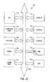
- FIG. 12illustrates another exemplary processor system which may include a segmented data bus 28 .
- the processor systemwhich may be a computer system 100 , for example, generally comprises a central processing unit (CPU) 102 , for example, a microprocessor, that communicates with one or more input/output (I/O) devices 112 , 114 , 116 over a system bus 122 .
- CPUcentral processing unit
- I/Oinput/output
- the computer system 100also includes random access memory (RAM) 118 , a read only memory (ROM) 120 and, in the case of a computer system may include peripheral devices such as a floppy disk drive 104 , a hard drive 106 , a display 108 and a compact disk (CD) ROM drive 110 which also communicate with the processor 102 over the bus 122 .
- the RAM 118includes memory devices communicating with a memory controller 31 via a segmented data bus 28 and associated receiver/driver pairs 212 , 214 constructed in accordance with the invention.
- This configuration of the computer system 100permits high speed communication and/or data transfer between different types of data devices, for example between the processor 102 and the memory controller 31 at the RAM 118 .
- FIG. 12is merely representative of many different types of processor system architectures which may employ the invention.
- segmented data bus 28has been described with reference to a digital data system, e.g., a memory system having memory modules 24 , 26 , the segmented data bus 28 can be used to transmit signals of any types, including analog, digital and radio frequency (RF) signals.
- RFradio frequency
Landscapes
- Engineering & Computer Science (AREA)
- Theoretical Computer Science (AREA)
- Physics & Mathematics (AREA)
- General Engineering & Computer Science (AREA)
- General Physics & Mathematics (AREA)
- Bus Control (AREA)
- Memory System (AREA)
Abstract
Description
Claims (48)
Priority Applications (1)
| Application Number | Priority Date | Filing Date | Title |
|---|---|---|---|
| US09/804,224US6882082B2 (en) | 2001-03-13 | 2001-03-13 | Memory repeater |
Applications Claiming Priority (1)
| Application Number | Priority Date | Filing Date | Title |
|---|---|---|---|
| US09/804,224US6882082B2 (en) | 2001-03-13 | 2001-03-13 | Memory repeater |
Publications (2)
| Publication Number | Publication Date |
|---|---|
| US20040225777A1 US20040225777A1 (en) | 2004-11-11 |
| US6882082B2true US6882082B2 (en) | 2005-04-19 |
Family
ID=33419011
Family Applications (1)
| Application Number | Title | Priority Date | Filing Date |
|---|---|---|---|
| US09/804,224Expired - LifetimeUS6882082B2 (en) | 2001-03-13 | 2001-03-13 | Memory repeater |
Country Status (1)
| Country | Link |
|---|---|
| US (1) | US6882082B2 (en) |
Cited By (59)
| Publication number | Priority date | Publication date | Assignee | Title |
|---|---|---|---|---|
| US20030097534A1 (en)* | 2001-11-21 | 2003-05-22 | Jeong Yong Gwon | Memory system using non-distributed command/address clock |
| US20040042496A1 (en)* | 2002-08-30 | 2004-03-04 | Intel Corporation | System including a segmentable, shared bus |
| US20040085795A1 (en)* | 2002-10-28 | 2004-05-06 | Georg Braun | Memory module and memory configuration with stub-free signal lines and distributed capacitive loads |
| US20040230759A1 (en)* | 2003-02-21 | 2004-11-18 | Georg Braun | Synchronous memory system and also method and protocol for communication in a synchronous memory system |
| US20050033905A1 (en)* | 2003-08-08 | 2005-02-10 | Leddige Michael W. | Split T-chain memory command and address bus topology |
| US20060083043A1 (en)* | 2003-11-17 | 2006-04-20 | Sun Microsystems, Inc. | Memory system topology |
| US20060095629A1 (en)* | 2004-10-29 | 2006-05-04 | International Business Machines Corporation | System, method and storage medium for providing a service interface to a memory system |
| US20060095701A1 (en)* | 2004-10-29 | 2006-05-04 | International Business Machines Corporation | System, method and storage medium for a memory subsystem with positional read data latency |
| US20060095620A1 (en)* | 2004-10-29 | 2006-05-04 | International Business Machines Corporation | System, method and storage medium for merging bus data in a memory subsystem |
| US20060250881A1 (en)* | 2003-09-30 | 2006-11-09 | Helmut Kandolf | Memory arrangement having a plurality of RAM chips |
| US20060290438A1 (en)* | 2004-02-27 | 2006-12-28 | Micron Technology, Inc. | Microstrip line dielectric overlay |
| US20070028028A1 (en)* | 2005-07-29 | 2007-02-01 | Paul Wallner | Semiconductor memory chip and memory system |
| US20070083701A1 (en)* | 2005-10-12 | 2007-04-12 | Sun Microsystems, Inc. | Power throttling in a memory system |
| US20070101086A1 (en)* | 2005-10-31 | 2007-05-03 | International Business Machines Corporation | System, method and storage medium for deriving clocks in a memory system |
| US20070124532A1 (en)* | 2005-04-21 | 2007-05-31 | Bennett Jon C | Interconnection system |
| US20070136537A1 (en)* | 2005-12-14 | 2007-06-14 | Sun Microsystems, Inc. | System memory board subsystem using dram with stacked dedicated high speed point to point links |
| US20070147115A1 (en)* | 2005-12-28 | 2007-06-28 | Fong-Long Lin | Unified memory and controller |
| US20070160053A1 (en)* | 2005-11-28 | 2007-07-12 | Coteus Paul W | Method and system for providing indeterminate read data latency in a memory system |
| US20070233933A1 (en)* | 2005-12-28 | 2007-10-04 | Jeremy Wang | Hard disk drive cache memory and playback device |
| US20070276977A1 (en)* | 2006-05-24 | 2007-11-29 | International Business Machines Corporation | Systems and methods for providing memory modules with multiple hub devices |
| US20070283077A1 (en)* | 2006-05-30 | 2007-12-06 | Christian Klein | Memory and Memory Communication System |
| US20070288707A1 (en)* | 2006-06-08 | 2007-12-13 | International Business Machines Corporation | Systems and methods for providing data modification operations in memory subsystems |
| US20080005479A1 (en)* | 2006-05-22 | 2008-01-03 | International Business Machines Corporation | Systems and methods for providing remote pre-fetch buffers |
| US20080016280A1 (en)* | 2004-10-29 | 2008-01-17 | International Business Machines Corporation | System, method and storage medium for providing data caching and data compression in a memory subsystem |
| US20080046795A1 (en)* | 2004-10-29 | 2008-02-21 | International Business Machines Corporation | System, method and storage medium for providing fault detection and correction in a memory subsystem |
| US20080065938A1 (en)* | 2004-10-29 | 2008-03-13 | International Business Machines Corporation | System, method and storage medium for testing a memory module |
| US7350048B1 (en) | 2004-10-28 | 2008-03-25 | Sun Microsystems, Inc. | Memory system topology |
| US20080104290A1 (en)* | 2004-10-29 | 2008-05-01 | International Business Machines Corporation | System, method and storage medium for providing a high speed test interface to a memory subsystem |
| US20080115137A1 (en)* | 2006-08-02 | 2008-05-15 | International Business Machines Corporation | Systems and methods for providing collision detection in a memory system |
| US20080177929A1 (en)* | 2004-10-29 | 2008-07-24 | International Business Machines Corporation | System, method and storage medium for a memory subsystem command interface |
| US20080183977A1 (en)* | 2007-01-29 | 2008-07-31 | International Business Machines Corporation | Systems and methods for providing a dynamic memory bank page policy |
| US20080291747A1 (en)* | 2007-05-24 | 2008-11-27 | Staktek Group L.P. | Buffered Memory Device |
| US7477522B2 (en) | 2006-10-23 | 2009-01-13 | International Business Machines Corporation | High density high reliability memory module with a fault tolerant address and command bus |
| US7490217B2 (en) | 2006-08-15 | 2009-02-10 | International Business Machines Corporation | Design structure for selecting memory busses according to physical memory organization information stored in virtual address translation tables |
| US20090043933A1 (en)* | 2006-10-23 | 2009-02-12 | Bennett Jon C R | Skew management in an interconnection system |
| US7493439B2 (en) | 2006-08-01 | 2009-02-17 | International Business Machines Corporation | Systems and methods for providing performance monitoring in a memory system |
| US20090070503A1 (en)* | 2000-08-11 | 2009-03-12 | Roy Greeff | Capacitive multidrop bus compensation |
| US20090070612A1 (en)* | 2005-04-21 | 2009-03-12 | Maxim Adelman | Memory power management |
| US7523282B1 (en) | 2005-10-27 | 2009-04-21 | Sun Microsystems, Inc. | Clock enable throttling for power savings in a memory subsystem |
| US7533212B1 (en) | 2005-10-20 | 2009-05-12 | Sun Microsystems, Inc. | System memory board subsystem using DRAM with integrated high speed point to point links |
| US7539810B2 (en) | 2004-07-30 | 2009-05-26 | International Business Machines Corporation | System, method and storage medium for a multi-mode memory buffer device |
| US7539842B2 (en) | 2006-08-15 | 2009-05-26 | International Business Machines Corporation | Computer memory system for selecting memory buses according to physical memory organization information stored in virtual address translation tables |
| US7539800B2 (en) | 2004-07-30 | 2009-05-26 | International Business Machines Corporation | System, method and storage medium for providing segment level sparing |
| US20090150707A1 (en)* | 2005-04-21 | 2009-06-11 | Drucker Kevin D | Mesosynchronous data bus apparatus and method of data transmission |
| US20090150599A1 (en)* | 2005-04-21 | 2009-06-11 | Bennett Jon C R | Method and system for storage of data in non-volatile media |
| US7581073B2 (en) | 2006-08-09 | 2009-08-25 | International Business Machines Corporation | Systems and methods for providing distributed autonomous power management in a memory system |
| US7587559B2 (en) | 2006-08-10 | 2009-09-08 | International Business Machines Corporation | Systems and methods for memory module power management |
| US7590882B2 (en) | 2004-10-29 | 2009-09-15 | International Business Machines Corporation | System, method and storage medium for bus calibration in a memory subsystem |
| US7594055B2 (en) | 2006-05-24 | 2009-09-22 | International Business Machines Corporation | Systems and methods for providing distributed technology independent memory controllers |
| US7603526B2 (en) | 2007-01-29 | 2009-10-13 | International Business Machines Corporation | Systems and methods for providing dynamic memory pre-fetch |
| US7721140B2 (en) | 2007-01-02 | 2010-05-18 | International Business Machines Corporation | Systems and methods for improving serviceability of a memory system |
| US7765368B2 (en) | 2004-07-30 | 2010-07-27 | International Business Machines Corporation | System, method and storage medium for providing a serialized memory interface with a bus repeater |
| US7868652B1 (en) | 2009-12-08 | 2011-01-11 | International Business Machines Corporation | Off-die termination module with a spring loaded pin in a DIMM socket |
| US7868651B1 (en) | 2009-12-08 | 2011-01-11 | International Business Machines Corporation | Off-die termination of memory module signal lines |
| US7870459B2 (en) | 2006-10-23 | 2011-01-11 | International Business Machines Corporation | High density high reliability memory module with power gating and a fault tolerant address and command bus |
| US20150131388A1 (en)* | 2013-11-11 | 2015-05-14 | Rambus Inc. | High capacity memory system using standard controller component |
| US9285865B2 (en) | 2012-06-29 | 2016-03-15 | Oracle International Corporation | Dynamic link scaling based on bandwidth utilization |
| US9286198B2 (en) | 2005-04-21 | 2016-03-15 | Violin Memory | Method and system for storage of data in non-volatile media |
| US9582449B2 (en) | 2005-04-21 | 2017-02-28 | Violin Memory, Inc. | Interconnection system |
Families Citing this family (1)
| Publication number | Priority date | Publication date | Assignee | Title |
|---|---|---|---|---|
| US9117037B2 (en)* | 2011-11-21 | 2015-08-25 | Acer Incorporated | Interface apparatus, cascading system thereof and cascading method thereof |
Citations (9)
| Publication number | Priority date | Publication date | Assignee | Title |
|---|---|---|---|---|
| US5081648A (en) | 1990-03-12 | 1992-01-14 | The Boeing Company | Current mode data bus digital communications system |
| US5623644A (en) | 1994-08-25 | 1997-04-22 | Intel Corporation | Point-to-point phase-tolerant communication |
| US5703806A (en)* | 1994-06-20 | 1997-12-30 | Neomagic Corporation | Graphics controller integrated circuit without memory interface |
| US5978880A (en)* | 1990-03-06 | 1999-11-02 | Xerox Corporation | Multi-segmented bus and method of operation |
| US6317352B1 (en)* | 2000-09-18 | 2001-11-13 | Intel Corporation | Apparatus for implementing a buffered daisy chain connection between a memory controller and memory modules |
| US6446174B1 (en)* | 2000-07-11 | 2002-09-03 | Intel Corporation | Computer system with dram bus |
| US6477614B1 (en)* | 1998-09-30 | 2002-11-05 | Intel Corporation | Method for implementing multiple memory buses on a memory module |
| US6493250B2 (en)* | 2000-12-28 | 2002-12-10 | Intel Corporation | Multi-tier point-to-point buffered memory interface |
| US6625687B1 (en)* | 2000-09-18 | 2003-09-23 | Intel Corporation | Memory module employing a junction circuit for point-to-point connection isolation, voltage translation, data synchronization, and multiplexing/demultiplexing |
- 2001
- 2001-03-13USUS09/804,224patent/US6882082B2/ennot_activeExpired - Lifetime
Patent Citations (10)
| Publication number | Priority date | Publication date | Assignee | Title |
|---|---|---|---|---|
| US5978880A (en)* | 1990-03-06 | 1999-11-02 | Xerox Corporation | Multi-segmented bus and method of operation |
| US5081648A (en) | 1990-03-12 | 1992-01-14 | The Boeing Company | Current mode data bus digital communications system |
| US5703806A (en)* | 1994-06-20 | 1997-12-30 | Neomagic Corporation | Graphics controller integrated circuit without memory interface |
| US5623644A (en) | 1994-08-25 | 1997-04-22 | Intel Corporation | Point-to-point phase-tolerant communication |
| US6477614B1 (en)* | 1998-09-30 | 2002-11-05 | Intel Corporation | Method for implementing multiple memory buses on a memory module |
| US6587912B2 (en)* | 1998-09-30 | 2003-07-01 | Intel Corporation | Method and apparatus for implementing multiple memory buses on a memory module |
| US6446174B1 (en)* | 2000-07-11 | 2002-09-03 | Intel Corporation | Computer system with dram bus |
| US6317352B1 (en)* | 2000-09-18 | 2001-11-13 | Intel Corporation | Apparatus for implementing a buffered daisy chain connection between a memory controller and memory modules |
| US6625687B1 (en)* | 2000-09-18 | 2003-09-23 | Intel Corporation | Memory module employing a junction circuit for point-to-point connection isolation, voltage translation, data synchronization, and multiplexing/demultiplexing |
| US6493250B2 (en)* | 2000-12-28 | 2002-12-10 | Intel Corporation | Multi-tier point-to-point buffered memory interface |
Non-Patent Citations (3)
| Title |
|---|
| "Hot Rod(TM) High-Speed Serial Link Gallium Arsenide," Gazelle Microcircuits, Inc. pp. 1-35. |
| Gustavson, D. "SCI Industrial Takeup and Future Developments," http://www.scizzl.com/Perspectives.html, 13 pages, reviewed Oct. 2, 2000. |
| Gustavson, D., "SCIzzL: The Local Area Memory Port," http://www.scizzl.com, 9 pages, reviewed Oct. 2, 2000. |
Cited By (126)
| Publication number | Priority date | Publication date | Assignee | Title |
|---|---|---|---|---|
| US20090070503A1 (en)* | 2000-08-11 | 2009-03-12 | Roy Greeff | Capacitive multidrop bus compensation |
| US7913005B2 (en)* | 2000-08-11 | 2011-03-22 | Round Rock Research, Llc | Capacitive multidrop bus compensation |
| US20030097534A1 (en)* | 2001-11-21 | 2003-05-22 | Jeong Yong Gwon | Memory system using non-distributed command/address clock |
| US7107476B2 (en)* | 2001-11-21 | 2006-09-12 | Hynix Semiconductor Inc. | Memory system using non-distributed command/address clock signals |
| US7360007B2 (en)* | 2002-08-30 | 2008-04-15 | Intel Corporation | System including a segmentable, shared bus |
| US20040042496A1 (en)* | 2002-08-30 | 2004-03-04 | Intel Corporation | System including a segmentable, shared bus |
| US20040085795A1 (en)* | 2002-10-28 | 2004-05-06 | Georg Braun | Memory module and memory configuration with stub-free signal lines and distributed capacitive loads |
| US20060202328A1 (en)* | 2002-10-28 | 2006-09-14 | Infineon Technologies Ag | Memory module and memory configuration with stub-free signal lines and distributed capacitive loads |
| US20040230759A1 (en)* | 2003-02-21 | 2004-11-18 | Georg Braun | Synchronous memory system and also method and protocol for communication in a synchronous memory system |
| US20050033905A1 (en)* | 2003-08-08 | 2005-02-10 | Leddige Michael W. | Split T-chain memory command and address bus topology |
| US7194572B2 (en)* | 2003-08-08 | 2007-03-20 | Intel Corporation | Memory system and method to reduce reflection and signal degradation |
| US7362650B2 (en)* | 2003-09-30 | 2008-04-22 | Infineon Technologies Ag | Memory arrangement having a plurality of RAM chips |
| US20060250881A1 (en)* | 2003-09-30 | 2006-11-09 | Helmut Kandolf | Memory arrangement having a plurality of RAM chips |
| US20060083043A1 (en)* | 2003-11-17 | 2006-04-20 | Sun Microsystems, Inc. | Memory system topology |
| US7533218B2 (en) | 2003-11-17 | 2009-05-12 | Sun Microsystems, Inc. | Memory system topology |
| US20060290438A1 (en)* | 2004-02-27 | 2006-12-28 | Micron Technology, Inc. | Microstrip line dielectric overlay |
| US20090025204A1 (en)* | 2004-02-27 | 2009-01-29 | Micron Technology, Inc. | Microstrip line dielectric overlay |
| US7436267B2 (en) | 2004-02-27 | 2008-10-14 | Micron Technology, Inc. | Microstrip line dielectric overlay |
| US7432774B2 (en) | 2004-02-27 | 2008-10-07 | Micron Technology, Inc. | Microstrip line dielectric overlay |
| US9214713B2 (en) | 2004-02-27 | 2015-12-15 | Micron Technology, Inc. | Method of fabricating a microstrip line dielectric overlay |
| US7539800B2 (en) | 2004-07-30 | 2009-05-26 | International Business Machines Corporation | System, method and storage medium for providing segment level sparing |
| US7539810B2 (en) | 2004-07-30 | 2009-05-26 | International Business Machines Corporation | System, method and storage medium for a multi-mode memory buffer device |
| US7765368B2 (en) | 2004-07-30 | 2010-07-27 | International Business Machines Corporation | System, method and storage medium for providing a serialized memory interface with a bus repeater |
| US7350048B1 (en) | 2004-10-28 | 2008-03-25 | Sun Microsystems, Inc. | Memory system topology |
| US8140942B2 (en) | 2004-10-29 | 2012-03-20 | International Business Machines Corporation | System, method and storage medium for providing fault detection and correction in a memory subsystem |
| US7610423B2 (en) | 2004-10-29 | 2009-10-27 | International Business Machines Corporation | Service interface to a memory system |
| US20060095620A1 (en)* | 2004-10-29 | 2006-05-04 | International Business Machines Corporation | System, method and storage medium for merging bus data in a memory subsystem |
| US20080016280A1 (en)* | 2004-10-29 | 2008-01-17 | International Business Machines Corporation | System, method and storage medium for providing data caching and data compression in a memory subsystem |
| US20080046795A1 (en)* | 2004-10-29 | 2008-02-21 | International Business Machines Corporation | System, method and storage medium for providing fault detection and correction in a memory subsystem |
| US20080046796A1 (en)* | 2004-10-29 | 2008-02-21 | International Business Machines Corporation | System, method and storage medium for providing fault detection and correction in a memory subsystem |
| US20080065938A1 (en)* | 2004-10-29 | 2008-03-13 | International Business Machines Corporation | System, method and storage medium for testing a memory module |
| US7844771B2 (en) | 2004-10-29 | 2010-11-30 | International Business Machines Corporation | System, method and storage medium for a memory subsystem command interface |
| US7512762B2 (en) | 2004-10-29 | 2009-03-31 | International Business Machines Corporation | System, method and storage medium for a memory subsystem with positional read data latency |
| US20060095701A1 (en)* | 2004-10-29 | 2006-05-04 | International Business Machines Corporation | System, method and storage medium for a memory subsystem with positional read data latency |
| US20080104290A1 (en)* | 2004-10-29 | 2008-05-01 | International Business Machines Corporation | System, method and storage medium for providing a high speed test interface to a memory subsystem |
| US7590882B2 (en) | 2004-10-29 | 2009-09-15 | International Business Machines Corporation | System, method and storage medium for bus calibration in a memory subsystem |
| US20080177929A1 (en)* | 2004-10-29 | 2008-07-24 | International Business Machines Corporation | System, method and storage medium for a memory subsystem command interface |
| US20060095629A1 (en)* | 2004-10-29 | 2006-05-04 | International Business Machines Corporation | System, method and storage medium for providing a service interface to a memory system |
| US7484161B2 (en) | 2004-10-29 | 2009-01-27 | International Business Machines Corporation | System, method and storage medium for providing fault detection and correction in a memory subsystem |
| US8589769B2 (en) | 2004-10-29 | 2013-11-19 | International Business Machines Corporation | System, method and storage medium for providing fault detection and correction in a memory subsystem |
| US7480759B2 (en) | 2004-10-29 | 2009-01-20 | International Business Machines Corporation | System, method and storage medium for providing data caching and data compression in a memory subsystem |
| US7441060B2 (en) | 2004-10-29 | 2008-10-21 | International Business Machines Corporation | System, method and storage medium for providing a service interface to a memory system |
| US7451273B2 (en) | 2004-10-29 | 2008-11-11 | International Business Machines Corporation | System, method and storage medium for providing data caching and data compression in a memory subsystem |
| US8296541B2 (en) | 2004-10-29 | 2012-10-23 | International Business Machines Corporation | Memory subsystem with positional read data latency |
| US7475316B2 (en) | 2004-10-29 | 2009-01-06 | International Business Machines Corporation | System, method and storage medium for providing a high speed test interface to a memory subsystem |
| US7480830B2 (en) | 2004-10-29 | 2009-01-20 | International Business Machines Corporation | System, method and storage medium for testing a memory module |
| US9286198B2 (en) | 2005-04-21 | 2016-03-15 | Violin Memory | Method and system for storage of data in non-volatile media |
| US9727263B2 (en) | 2005-04-21 | 2017-08-08 | Violin Memory, Inc. | Method and system for storage of data in a non-volatile media |
| US8452929B2 (en) | 2005-04-21 | 2013-05-28 | Violin Memory Inc. | Method and system for storage of data in non-volatile media |
| US8726064B2 (en) | 2005-04-21 | 2014-05-13 | Violin Memory Inc. | Interconnection system |
| US8112655B2 (en) | 2005-04-21 | 2012-02-07 | Violin Memory, Inc. | Mesosynchronous data bus apparatus and method of data transmission |
| US10176861B2 (en) | 2005-04-21 | 2019-01-08 | Violin Systems Llc | RAIDed memory system management |
| US20090150599A1 (en)* | 2005-04-21 | 2009-06-11 | Bennett Jon C R | Method and system for storage of data in non-volatile media |
| US9384818B2 (en) | 2005-04-21 | 2016-07-05 | Violin Memory | Memory power management |
| US10417159B2 (en) | 2005-04-21 | 2019-09-17 | Violin Systems Llc | Interconnection system |
| US20070124532A1 (en)* | 2005-04-21 | 2007-05-31 | Bennett Jon C | Interconnection system |
| US20090070612A1 (en)* | 2005-04-21 | 2009-03-12 | Maxim Adelman | Memory power management |
| US20090150707A1 (en)* | 2005-04-21 | 2009-06-11 | Drucker Kevin D | Mesosynchronous data bus apparatus and method of data transmission |
| US9582449B2 (en) | 2005-04-21 | 2017-02-28 | Violin Memory, Inc. | Interconnection system |
| DE102006032343B4 (en)* | 2005-07-29 | 2010-12-02 | Qimonda Ag | Semiconductor memory interface |
| US8108643B2 (en) | 2005-07-29 | 2012-01-31 | Qimonda Ag | Semiconductor memory chip and memory system |
| US20070028028A1 (en)* | 2005-07-29 | 2007-02-01 | Paul Wallner | Semiconductor memory chip and memory system |
| US7496777B2 (en) | 2005-10-12 | 2009-02-24 | Sun Microsystems, Inc. | Power throttling in a memory system |
| US20070083701A1 (en)* | 2005-10-12 | 2007-04-12 | Sun Microsystems, Inc. | Power throttling in a memory system |
| US7533212B1 (en) | 2005-10-20 | 2009-05-12 | Sun Microsystems, Inc. | System memory board subsystem using DRAM with integrated high speed point to point links |
| US7523282B1 (en) | 2005-10-27 | 2009-04-21 | Sun Microsystems, Inc. | Clock enable throttling for power savings in a memory subsystem |
| US7934115B2 (en) | 2005-10-31 | 2011-04-26 | International Business Machines Corporation | Deriving clocks in a memory system |
| US20070101086A1 (en)* | 2005-10-31 | 2007-05-03 | International Business Machines Corporation | System, method and storage medium for deriving clocks in a memory system |
| US7478259B2 (en)* | 2005-10-31 | 2009-01-13 | International Business Machines Corporation | System, method and storage medium for deriving clocks in a memory system |
| US8151042B2 (en) | 2005-11-28 | 2012-04-03 | International Business Machines Corporation | Method and system for providing identification tags in a memory system having indeterminate data response times |
| US7685392B2 (en) | 2005-11-28 | 2010-03-23 | International Business Machines Corporation | Providing indeterminate read data latency in a memory system |
| US20070286199A1 (en)* | 2005-11-28 | 2007-12-13 | International Business Machines Corporation | Method and system for providing identification tags in a memory system having indeterminate data response times |
| US8327105B2 (en) | 2005-11-28 | 2012-12-04 | International Business Machines Corporation | Providing frame start indication in a memory system having indeterminate read data latency |
| US8495328B2 (en) | 2005-11-28 | 2013-07-23 | International Business Machines Corporation | Providing frame start indication in a memory system having indeterminate read data latency |
| US20070160053A1 (en)* | 2005-11-28 | 2007-07-12 | Coteus Paul W | Method and system for providing indeterminate read data latency in a memory system |
| US8145868B2 (en) | 2005-11-28 | 2012-03-27 | International Business Machines Corporation | Method and system for providing frame start indication in a memory system having indeterminate read data latency |
| US20070136537A1 (en)* | 2005-12-14 | 2007-06-14 | Sun Microsystems, Inc. | System memory board subsystem using dram with stacked dedicated high speed point to point links |
| US7409491B2 (en) | 2005-12-14 | 2008-08-05 | Sun Microsystems, Inc. | System memory board subsystem using DRAM with stacked dedicated high speed point to point links |
| US20090150588A1 (en)* | 2005-12-28 | 2009-06-11 | Silicon Storage Technology, Inc. | Hard Disk Drive Cache Memory and Playback Device |
| US7519754B2 (en)* | 2005-12-28 | 2009-04-14 | Silicon Storage Technology, Inc. | Hard disk drive cache memory and playback device |
| US20070147115A1 (en)* | 2005-12-28 | 2007-06-28 | Fong-Long Lin | Unified memory and controller |
| US20070233933A1 (en)* | 2005-12-28 | 2007-10-04 | Jeremy Wang | Hard disk drive cache memory and playback device |
| US7636813B2 (en) | 2006-05-22 | 2009-12-22 | International Business Machines Corporation | Systems and methods for providing remote pre-fetch buffers |
| US20080005479A1 (en)* | 2006-05-22 | 2008-01-03 | International Business Machines Corporation | Systems and methods for providing remote pre-fetch buffers |
| US20070276977A1 (en)* | 2006-05-24 | 2007-11-29 | International Business Machines Corporation | Systems and methods for providing memory modules with multiple hub devices |
| US7594055B2 (en) | 2006-05-24 | 2009-09-22 | International Business Machines Corporation | Systems and methods for providing distributed technology independent memory controllers |
| US7640386B2 (en) | 2006-05-24 | 2009-12-29 | International Business Machines Corporation | Systems and methods for providing memory modules with multiple hub devices |
| US8352695B2 (en)* | 2006-05-30 | 2013-01-08 | Lantiq Deutschland Gmbh | Selectable access rates in a memory and memory communication system |
| US20070283077A1 (en)* | 2006-05-30 | 2007-12-06 | Christian Klein | Memory and Memory Communication System |
| US20070288707A1 (en)* | 2006-06-08 | 2007-12-13 | International Business Machines Corporation | Systems and methods for providing data modification operations in memory subsystems |
| US7584336B2 (en) | 2006-06-08 | 2009-09-01 | International Business Machines Corporation | Systems and methods for providing data modification operations in memory subsystems |
| US7493439B2 (en) | 2006-08-01 | 2009-02-17 | International Business Machines Corporation | Systems and methods for providing performance monitoring in a memory system |
| US7669086B2 (en) | 2006-08-02 | 2010-02-23 | International Business Machines Corporation | Systems and methods for providing collision detection in a memory system |
| US20080115137A1 (en)* | 2006-08-02 | 2008-05-15 | International Business Machines Corporation | Systems and methods for providing collision detection in a memory system |
| US7581073B2 (en) | 2006-08-09 | 2009-08-25 | International Business Machines Corporation | Systems and methods for providing distributed autonomous power management in a memory system |
| US7587559B2 (en) | 2006-08-10 | 2009-09-08 | International Business Machines Corporation | Systems and methods for memory module power management |
| US7539842B2 (en) | 2006-08-15 | 2009-05-26 | International Business Machines Corporation | Computer memory system for selecting memory buses according to physical memory organization information stored in virtual address translation tables |
| US7636833B2 (en) | 2006-08-15 | 2009-12-22 | International Business Machines Corporation | Method for selecting memory busses according to physical memory organization information associated with virtual address translation tables |
| US7490217B2 (en) | 2006-08-15 | 2009-02-10 | International Business Machines Corporation | Design structure for selecting memory busses according to physical memory organization information stored in virtual address translation tables |
| US20110060857A1 (en)* | 2006-10-23 | 2011-03-10 | Violin Memory, Inc. | Skew management in an interconnection system |
| US8090973B2 (en) | 2006-10-23 | 2012-01-03 | Violin Memory, Inc. | Skew management in an interconnection system |
| US8028186B2 (en) | 2006-10-23 | 2011-09-27 | Violin Memory, Inc. | Skew management in an interconnection system |
| US8381064B2 (en) | 2006-10-23 | 2013-02-19 | International Business Machines Corporation | High density high reliability memory module with power gating and a fault tolerant address and command bus |
| US20090043933A1 (en)* | 2006-10-23 | 2009-02-12 | Bennett Jon C R | Skew management in an interconnection system |
| US7477522B2 (en) | 2006-10-23 | 2009-01-13 | International Business Machines Corporation | High density high reliability memory module with a fault tolerant address and command bus |
| US7870459B2 (en) | 2006-10-23 | 2011-01-11 | International Business Machines Corporation | High density high reliability memory module with power gating and a fault tolerant address and command bus |
| US8806262B2 (en) | 2006-10-23 | 2014-08-12 | Violin Memory, Inc. | Skew management in an interconnection system |
| US7721140B2 (en) | 2007-01-02 | 2010-05-18 | International Business Machines Corporation | Systems and methods for improving serviceability of a memory system |
| US20080183977A1 (en)* | 2007-01-29 | 2008-07-31 | International Business Machines Corporation | Systems and methods for providing a dynamic memory bank page policy |
| US7606988B2 (en) | 2007-01-29 | 2009-10-20 | International Business Machines Corporation | Systems and methods for providing a dynamic memory bank page policy |
| US7603526B2 (en) | 2007-01-29 | 2009-10-13 | International Business Machines Corporation | Systems and methods for providing dynamic memory pre-fetch |
| US20080291747A1 (en)* | 2007-05-24 | 2008-11-27 | Staktek Group L.P. | Buffered Memory Device |
| US7508723B2 (en) | 2007-05-24 | 2009-03-24 | Entorian Technologies, Lp | Buffered memory device |
| US7868651B1 (en) | 2009-12-08 | 2011-01-11 | International Business Machines Corporation | Off-die termination of memory module signal lines |
| US7868652B1 (en) | 2009-12-08 | 2011-01-11 | International Business Machines Corporation | Off-die termination module with a spring loaded pin in a DIMM socket |
| US9285865B2 (en) | 2012-06-29 | 2016-03-15 | Oracle International Corporation | Dynamic link scaling based on bandwidth utilization |
| US9165639B2 (en)* | 2013-11-11 | 2015-10-20 | Rambus Inc. | High capacity memory system using standard controller component |
| US11568919B2 (en) | 2013-11-11 | 2023-01-31 | Rambus Inc. | High capacity memory system using standard controller component |
| US9653146B2 (en)* | 2013-11-11 | 2017-05-16 | Rambus Inc. | High capacity memory system using standard controller component |
| US20150138895A1 (en)* | 2013-11-11 | 2015-05-21 | Rambus Inc. | High capacity memory system using standard controller component |
| US20150131388A1 (en)* | 2013-11-11 | 2015-05-14 | Rambus Inc. | High capacity memory system using standard controller component |
| US10453517B2 (en)* | 2013-11-11 | 2019-10-22 | Rambus Inc. | High capacity memory system using controller component |
| US11024362B2 (en) | 2013-11-11 | 2021-06-01 | Rambus Inc. | High capacity memory system using standard controller component |
| US9183920B2 (en)* | 2013-11-11 | 2015-11-10 | Rambus Inc. | High capacity memory system using standard controller component |
| US11823732B2 (en) | 2013-11-11 | 2023-11-21 | Rambus Inc. | High capacity memory system using standard controller component |
| US12148462B2 (en) | 2013-11-11 | 2024-11-19 | Rambus Inc. | High capacity memory system using standard controller component |
Also Published As
| Publication number | Publication date |
|---|---|
| US20040225777A1 (en) | 2004-11-11 |
Similar Documents
| Publication | Publication Date | Title |
|---|---|---|
| US6882082B2 (en) | Memory repeater | |
| US6934785B2 (en) | High speed interface with looped bus | |
| US7051151B2 (en) | Integrated circuit buffer device | |
| US7320047B2 (en) | System having a controller device, a buffer device and a plurality of memory devices | |
| US7526597B2 (en) | Buffered memory having a control bus and dedicated data lines | |
| JP4142950B2 (en) | Apparatus for achieving a buffered daisy chain connection between a memory controller and a memory module | |
| US7194593B2 (en) | Memory hub with integrated non-volatile memory | |
| US7610447B2 (en) | Upgradable memory system with reconfigurable interconnect | |
| US20050166026A1 (en) | Configurable width buffered module having switch elements | |
| US9734116B2 (en) | Method, apparatus and system for configuring a protocol stack of an integrated circuit chip | |
| KR100756094B1 (en) | Arrangement for the transmission of signals between a data processing unit and a functional unit | |
| JPH1131031A (en) | Bus module |
Legal Events
| Date | Code | Title | Description |
|---|---|---|---|
| AS | Assignment | Owner name:MICRON TECHNOLOGY, INC., IDAHO Free format text:ASSIGNMENT OF ASSIGNORS INTEREST;ASSIGNORS:GREEFF, ROY;OVARD, DAVID;REEL/FRAME:011609/0833 Effective date:20010302 | |
| STCF | Information on status: patent grant | Free format text:PATENTED CASE | |
| FEPP | Fee payment procedure | Free format text:PAYER NUMBER DE-ASSIGNED (ORIGINAL EVENT CODE: RMPN); ENTITY STATUS OF PATENT OWNER: LARGE ENTITY Free format text:PAYOR NUMBER ASSIGNED (ORIGINAL EVENT CODE: ASPN); ENTITY STATUS OF PATENT OWNER: LARGE ENTITY | |
| FPAY | Fee payment | Year of fee payment:4 | |
| FPAY | Fee payment | Year of fee payment:8 | |
| AS | Assignment | Owner name:U.S. BANK NATIONAL ASSOCIATION, AS COLLATERAL AGENT, CALIFORNIA Free format text:SECURITY INTEREST;ASSIGNOR:MICRON TECHNOLOGY, INC.;REEL/FRAME:038669/0001 Effective date:20160426 Owner name:U.S. BANK NATIONAL ASSOCIATION, AS COLLATERAL AGEN Free format text:SECURITY INTEREST;ASSIGNOR:MICRON TECHNOLOGY, INC.;REEL/FRAME:038669/0001 Effective date:20160426 | |
| AS | Assignment | Owner name:MORGAN STANLEY SENIOR FUNDING, INC., AS COLLATERAL AGENT, MARYLAND Free format text:PATENT SECURITY AGREEMENT;ASSIGNOR:MICRON TECHNOLOGY, INC.;REEL/FRAME:038954/0001 Effective date:20160426 Owner name:MORGAN STANLEY SENIOR FUNDING, INC., AS COLLATERAL Free format text:PATENT SECURITY AGREEMENT;ASSIGNOR:MICRON TECHNOLOGY, INC.;REEL/FRAME:038954/0001 Effective date:20160426 | |
| FPAY | Fee payment | Year of fee payment:12 | |
| AS | Assignment | Owner name:U.S. BANK NATIONAL ASSOCIATION, AS COLLATERAL AGENT, CALIFORNIA Free format text:CORRECTIVE ASSIGNMENT TO CORRECT THE REPLACE ERRONEOUSLY FILED PATENT #7358718 WITH THE CORRECT PATENT #7358178 PREVIOUSLY RECORDED ON REEL 038669 FRAME 0001. ASSIGNOR(S) HEREBY CONFIRMS THE SECURITY INTEREST;ASSIGNOR:MICRON TECHNOLOGY, INC.;REEL/FRAME:043079/0001 Effective date:20160426 Owner name:U.S. BANK NATIONAL ASSOCIATION, AS COLLATERAL AGEN Free format text:CORRECTIVE ASSIGNMENT TO CORRECT THE REPLACE ERRONEOUSLY FILED PATENT #7358718 WITH THE CORRECT PATENT #7358178 PREVIOUSLY RECORDED ON REEL 038669 FRAME 0001. ASSIGNOR(S) HEREBY CONFIRMS THE SECURITY INTEREST;ASSIGNOR:MICRON TECHNOLOGY, INC.;REEL/FRAME:043079/0001 Effective date:20160426 | |
| AS | Assignment | Owner name:JPMORGAN CHASE BANK, N.A., AS COLLATERAL AGENT, ILLINOIS Free format text:SECURITY INTEREST;ASSIGNORS:MICRON TECHNOLOGY, INC.;MICRON SEMICONDUCTOR PRODUCTS, INC.;REEL/FRAME:047540/0001 Effective date:20180703 Owner name:JPMORGAN CHASE BANK, N.A., AS COLLATERAL AGENT, IL Free format text:SECURITY INTEREST;ASSIGNORS:MICRON TECHNOLOGY, INC.;MICRON SEMICONDUCTOR PRODUCTS, INC.;REEL/FRAME:047540/0001 Effective date:20180703 | |
| AS | Assignment | Owner name:MICRON TECHNOLOGY, INC., IDAHO Free format text:RELEASE BY SECURED PARTY;ASSIGNOR:U.S. BANK NATIONAL ASSOCIATION, AS COLLATERAL AGENT;REEL/FRAME:047243/0001 Effective date:20180629 | |
| AS | Assignment | Owner name:MICRON TECHNOLOGY, INC., IDAHO Free format text:RELEASE BY SECURED PARTY;ASSIGNOR:MORGAN STANLEY SENIOR FUNDING, INC., AS COLLATERAL AGENT;REEL/FRAME:050937/0001 Effective date:20190731 | |
| AS | Assignment | Owner name:MICRON TECHNOLOGY, INC., IDAHO Free format text:RELEASE BY SECURED PARTY;ASSIGNOR:JPMORGAN CHASE BANK, N.A., AS COLLATERAL AGENT;REEL/FRAME:051028/0001 Effective date:20190731 Owner name:MICRON SEMICONDUCTOR PRODUCTS, INC., IDAHO Free format text:RELEASE BY SECURED PARTY;ASSIGNOR:JPMORGAN CHASE BANK, N.A., AS COLLATERAL AGENT;REEL/FRAME:051028/0001 Effective date:20190731 |