US6878467B2 - Organic electro-luminescence element used in a display device - Google Patents
Organic electro-luminescence element used in a display deviceDownload PDFInfo
- Publication number
- US6878467B2 US6878467B2US09/970,068US97006801AUS6878467B2US 6878467 B2US6878467 B2US 6878467B2US 97006801 AUS97006801 AUS 97006801AUS 6878467 B2US6878467 B2US 6878467B2
- Authority
- US
- United States
- Prior art keywords
- organic
- layer
- glass substrate
- rim
- element according
- Prior art date
- Legal status (The legal status is an assumption and is not a legal conclusion. Google has not performed a legal analysis and makes no representation as to the accuracy of the status listed.)
- Expired - Lifetime, expires
Links
- 238000005401electroluminescenceMethods0.000titleclaimsabstractdescription57
- 238000007789sealingMethods0.000claimsabstractdescription48
- 239000000758substrateSubstances0.000claimsabstractdescription46
- 239000011521glassSubstances0.000claimsabstractdescription42
- 238000001035dryingMethods0.000claimsabstractdescription41
- 239000002131composite materialSubstances0.000claimsdescription18
- QVGXLLKOCUKJST-UHFFFAOYSA-Natomic oxygenChemical compound[O]QVGXLLKOCUKJST-UHFFFAOYSA-N0.000claimsdescription16
- 239000001301oxygenSubstances0.000claimsdescription16
- 229910052760oxygenInorganic materials0.000claimsdescription16
- VYPSYNLAJGMNEJ-UHFFFAOYSA-NSilicium dioxideChemical compoundO=[Si]=OVYPSYNLAJGMNEJ-UHFFFAOYSA-N0.000claimsdescription15
- 239000003795chemical substances by applicationSubstances0.000claimsdescription15
- 229920005989resinPolymers0.000claimsdescription14
- 239000011347resinSubstances0.000claimsdescription14
- ODINCKMPIJJUCX-UHFFFAOYSA-Ncalcium oxideInorganic materials[Ca]=OODINCKMPIJJUCX-UHFFFAOYSA-N0.000claimsdescription13
- 239000000463materialSubstances0.000claimsdescription13
- 239000012535impuritySubstances0.000claimsdescription11
- 238000010521absorption reactionMethods0.000claimsdescription10
- XLYOFNOQVPJJNP-UHFFFAOYSA-NwaterSubstancesOXLYOFNOQVPJJNP-UHFFFAOYSA-N0.000claimsdescription10
- 238000003848UV Light-CuringMethods0.000claimsdescription7
- PNEYBMLMFCGWSK-UHFFFAOYSA-Naluminium oxideInorganic materials[O-2].[O-2].[O-2].[Al+3].[Al+3]PNEYBMLMFCGWSK-UHFFFAOYSA-N0.000claimsdescription7
- 229910052681coesiteInorganic materials0.000claimsdescription7
- 229910052593corundumInorganic materials0.000claimsdescription7
- 229910052906cristobaliteInorganic materials0.000claimsdescription7
- 229910052710siliconInorganic materials0.000claimsdescription7
- 239000010703siliconSubstances0.000claimsdescription7
- 239000000377silicon dioxideSubstances0.000claimsdescription7
- 229910052682stishoviteInorganic materials0.000claimsdescription7
- 229910052905tridymiteInorganic materials0.000claimsdescription7
- 229910001845yogo sapphireInorganic materials0.000claimsdescription7
- 238000003475laminationMethods0.000claimsdescription6
- 230000035699permeabilityEffects0.000claimsdescription6
- 239000011368organic materialSubstances0.000claimsdescription5
- 230000002209hydrophobic effectEffects0.000claimsdescription4
- 229910010272inorganic materialInorganic materials0.000claims4
- 239000011147inorganic materialSubstances0.000claims4
- 238000001179sorption measurementMethods0.000claims3
- 239000010410layerSubstances0.000description50
- 238000000034methodMethods0.000description7
- 238000004806packaging method and processMethods0.000description7
- 239000012298atmosphereSubstances0.000description5
- 238000010943off-gassingMethods0.000description5
- 239000000126substanceSubstances0.000description5
- 239000002904solventSubstances0.000description4
- 239000002274desiccantSubstances0.000description3
- 229910052751metalInorganic materials0.000description3
- 239000002184metalSubstances0.000description3
- 229920000642polymerPolymers0.000description3
- 230000002265preventionEffects0.000description3
- 230000005611electricityEffects0.000description2
- 239000007787solidSubstances0.000description2
- -1BaOChemical class0.000description1
- UXVMQQNJUSDDNG-UHFFFAOYSA-LCalcium chlorideChemical compound[Cl-].[Cl-].[Ca+2]UXVMQQNJUSDDNG-UHFFFAOYSA-L0.000description1
- KRHYYFGTRYWZRS-UHFFFAOYSA-MFluoride anionChemical compound[F-]KRHYYFGTRYWZRS-UHFFFAOYSA-M0.000description1
- OAICVXFJPJFONN-UHFFFAOYSA-NPhosphorusChemical compound[P]OAICVXFJPJFONN-UHFFFAOYSA-N0.000description1
- UCKMPCXJQFINFW-UHFFFAOYSA-NSulphideChemical compound[S-2]UCKMPCXJQFINFW-UHFFFAOYSA-N0.000description1
- 229910052925anhydriteInorganic materials0.000description1
- QVQLCTNNEUAWMS-UHFFFAOYSA-Nbarium oxideInorganic materials[Ba]=OQVQLCTNNEUAWMS-UHFFFAOYSA-N0.000description1
- 239000007767bonding agentSubstances0.000description1
- 239000001110calcium chlorideSubstances0.000description1
- 229910001628calcium chlorideInorganic materials0.000description1
- OSGAYBCDTDRGGQ-UHFFFAOYSA-Lcalcium sulfateChemical compound[Ca+2].[O-]S([O-])(=O)=OOSGAYBCDTDRGGQ-UHFFFAOYSA-L0.000description1
- 150000001875compoundsChemical class0.000description1
- 239000004020conductorSubstances0.000description1
- 229920001577copolymerPolymers0.000description1
- 238000005336crackingMethods0.000description1
- 230000003247decreasing effectEffects0.000description1
- 238000000151depositionMethods0.000description1
- 238000010586diagramMethods0.000description1
- 238000004090dissolutionMethods0.000description1
- 238000005516engineering processMethods0.000description1
- 239000003822epoxy resinSubstances0.000description1
- 230000009477glass transitionEffects0.000description1
- AMGQUBHHOARCQH-UHFFFAOYSA-Nindium;oxotinChemical compound[In].[Sn]=OAMGQUBHHOARCQH-UHFFFAOYSA-N0.000description1
- 239000011261inert gasSubstances0.000description1
- 238000004020luminiscence typeMethods0.000description1
- 229910001512metal fluorideInorganic materials0.000description1
- 229910044991metal oxideInorganic materials0.000description1
- 150000004706metal oxidesChemical class0.000description1
- 229910052976metal sulfideInorganic materials0.000description1
- 239000012044organic layerSubstances0.000description1
- 230000003647oxidationEffects0.000description1
- 238000007254oxidation reactionMethods0.000description1
- 238000012858packaging processMethods0.000description1
- 229910052698phosphorusInorganic materials0.000description1
- 239000011574phosphorusSubstances0.000description1
- 238000007747platingMethods0.000description1
- 229920000647polyepoxidePolymers0.000description1
- 238000007639printingMethods0.000description1
- 229910052814silicon oxideInorganic materials0.000description1
Images


Classifications
- H—ELECTRICITY
- H05—ELECTRIC TECHNIQUES NOT OTHERWISE PROVIDED FOR
- H05B—ELECTRIC HEATING; ELECTRIC LIGHT SOURCES NOT OTHERWISE PROVIDED FOR; CIRCUIT ARRANGEMENTS FOR ELECTRIC LIGHT SOURCES, IN GENERAL
- H05B33/00—Electroluminescent light sources
- H05B33/02—Details
- H05B33/04—Sealing arrangements, e.g. against humidity
- H—ELECTRICITY
- H10—SEMICONDUCTOR DEVICES; ELECTRIC SOLID-STATE DEVICES NOT OTHERWISE PROVIDED FOR
- H10K—ORGANIC ELECTRIC SOLID-STATE DEVICES
- H10K50/00—Organic light-emitting devices
- H10K50/80—Constructional details
- H10K50/84—Passivation; Containers; Encapsulations
- H10K50/842—Containers
- H10K50/8426—Peripheral sealing arrangements, e.g. adhesives, sealants
- H—ELECTRICITY
- H10—SEMICONDUCTOR DEVICES; ELECTRIC SOLID-STATE DEVICES NOT OTHERWISE PROVIDED FOR
- H10K—ORGANIC ELECTRIC SOLID-STATE DEVICES
- H10K50/00—Organic light-emitting devices
- H10K50/80—Constructional details
- H10K50/84—Passivation; Containers; Encapsulations
- H10K50/846—Passivation; Containers; Encapsulations comprising getter material or desiccants
- H—ELECTRICITY
- H10—SEMICONDUCTOR DEVICES; ELECTRIC SOLID-STATE DEVICES NOT OTHERWISE PROVIDED FOR
- H10K—ORGANIC ELECTRIC SOLID-STATE DEVICES
- H10K59/00—Integrated devices, or assemblies of multiple devices, comprising at least one organic light-emitting element covered by group H10K50/00
- H10K59/80—Constructional details
- H10K59/87—Passivation; Containers; Encapsulations
- H10K59/871—Self-supporting sealing arrangements
- H10K59/8722—Peripheral sealing arrangements, e.g. adhesives, sealants
- H—ELECTRICITY
- H10—SEMICONDUCTOR DEVICES; ELECTRIC SOLID-STATE DEVICES NOT OTHERWISE PROVIDED FOR
- H10K—ORGANIC ELECTRIC SOLID-STATE DEVICES
- H10K59/00—Integrated devices, or assemblies of multiple devices, comprising at least one organic light-emitting element covered by group H10K50/00
- H10K59/80—Constructional details
- H10K59/87—Passivation; Containers; Encapsulations
- H10K59/874—Passivation; Containers; Encapsulations including getter material or desiccant
- Y—GENERAL TAGGING OF NEW TECHNOLOGICAL DEVELOPMENTS; GENERAL TAGGING OF CROSS-SECTIONAL TECHNOLOGIES SPANNING OVER SEVERAL SECTIONS OF THE IPC; TECHNICAL SUBJECTS COVERED BY FORMER USPC CROSS-REFERENCE ART COLLECTIONS [XRACs] AND DIGESTS
- Y10—TECHNICAL SUBJECTS COVERED BY FORMER USPC
- Y10S—TECHNICAL SUBJECTS COVERED BY FORMER USPC CROSS-REFERENCE ART COLLECTIONS [XRACs] AND DIGESTS
- Y10S428/00—Stock material or miscellaneous articles
- Y10S428/917—Electroluminescent
- Y—GENERAL TAGGING OF NEW TECHNOLOGICAL DEVELOPMENTS; GENERAL TAGGING OF CROSS-SECTIONAL TECHNOLOGIES SPANNING OVER SEVERAL SECTIONS OF THE IPC; TECHNICAL SUBJECTS COVERED BY FORMER USPC CROSS-REFERENCE ART COLLECTIONS [XRACs] AND DIGESTS
- Y10—TECHNICAL SUBJECTS COVERED BY FORMER USPC
- Y10T—TECHNICAL SUBJECTS COVERED BY FORMER US CLASSIFICATION
- Y10T428/00—Stock material or miscellaneous articles
- Y10T428/23—Sheet including cover or casing
- Y10T428/239—Complete cover or casing
Definitions
- the present inventionrelates to an organic electro-luminescence (EL) element used in a display device and, more particularly, to a method of packaging an organic EL element used in a display device.
- ELorganic electro-luminescence
- EL elementsIn an electro-luminescence (EL) element used for a display device, electric current applied to specific fluorescence or phosphorus can transform electricity into luminosity.
- EL elementsare classified as organic and inorganic, wherein the organic EL element employs laminated organic layers and has the advantages of thin profile, light weight, high luminescent efficiency, and low driving voltage.
- the probability of moisture and oxygen permeating the organic EL elementalso increases, causing detachment between the organic luminescent layer and the cathode electrode, cracking of the organic materials, and oxidation of the electrodes.
- a so-called ‘dark spot’to which electricity is not supplied, is generated, decreasing luminescence and luminescent uniformity.
- a sealing caseis commonly used to package the glass substrate on which metal electrodes and the organic luminescent layer are completed. Also, in order to prolong the active lifetime, a desiccant is installed to absorb the moisture and impurities generated in the interior space, the water and oxygen permeating from the atmosphere, and the moisture generated from the outgassing caused by the bonding agent on the rim of the sealing case.
- U.S. Pat. No. 5,882,761discloses an organic EL element 10 , which comprises a glass substrate 12 , a sealing agent 14 of UV-curing resin formed on the rim of the glass substrate 12 , and a sealing case 16 bonded to the glass substrate 12 by the sealing agent 14 .
- the internal space formed by the glass substrate 12 and the sealing case 16becomes an airtight container.
- the glass substrate 12comprises a lamination body 20 that is formed by a cathode layer 26 , an organic luminescent material layer 24 and an anode layer 22 .
- a drying substance 28is disposed on the bottom of the sealing case 16 and spaced from the lamination body 20 by an internal space 18 that is filled with dried inert gas.
- the drying substance 28comprises a solid compound, such as BaO, CaO, CaSO 4 , and CaCl 2 , which chemically absorbs moisture and maintains its solid state.
- the UV-curing resin used in the sealing agent 14is epoxy resin that has good adhesion but poor resistance to moisture in the internal space 18 caused by outgassing of the sealing agent 14 and the permeation of water and oxygen from the atmosphere. This may compromise the luminescent properties of the organic EL element 10 .
- one methodis to develop a new material for the sealing agent 14 to achieve good adhesion and good water/oxygen-resistance ability. Yet, in consideration of the thermal expansion coefficient match, the glass transition temperature and the contact angle, adequate material has yet to be developed for the sealing agent 14 .
- the other methodis to add a large number of BaO or CaO to the drying substance 28 to increase the moisture absorbency. Unfortunately, the moisture absorbency is limited when the thickness of the drying substance 28 exceeds a critical value. Thus, a new method of packaging the organic EL element solving the aforementioned problems is called for.
- the present inventionprovides an organic EL element used for a display device with adequate packaging method to solve the problems in the prior art.
- the organic electro-luminescence (EL) element used for a display devicehas a glass substrate having a luminescent device on the inner surface, a drying layer formed on the rim of the inner surface of the glass substrate, a sealing layer formed on the rim of the inner surface of the glass substrate and surrounding the drying layer, and a sealing case bonded to the rim of the glass substrate to form an airtight space.
- the drying layercomprises an adhesion agent and composite materials with absorption of moisture, oxygen and impurities, wherein the adhesion agent is UV-curing resin and the composite material is inorganic absorption material or organic absorption material.
- the composite materialcomprises silicon, Al 2 O 3 , CaO and SiO 2 .
- the sealing casecomprises a trench on the bottom of the inner wall and in position to the luminescent device, a hydrophobic layer in the bottom of the trench, an adhesion layer formed on the rim of the opening of the trench; and a semi-permeable film with moisture permeability without water permeability covering the opening of the trench and bonded by the adhesion layer.
- the adhesion layercomprises an adhesion agent and composite materials with absorption of moisture, oxygen and impurities.
- Yet another object of the inventionis to provide a drying layer that has adhesion, resistance to moisture and oxygen permeated from the atmosphere, the absorption of impurities and solvents generated in the airtight space, and prevention of the outgassing problem caused by the resin material.
- Still another object of the inventionis to provide a semi-permeable film to stop the water droplets remaining in the trench from permeating the airtight space of the organic EL element.
- Another object of the inventionis to share the absorption of the moisture between the drying layer and the specific sealing case, thereby increasing the active lifetime of the drying layer.
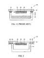
- FIG. 1is a schematic diagram showing an organic EL element according to the prior art.
- FIG. 2is a schematic cross-section showing an organic EL element used for a display device according to the first embodiment of the present invention.
- FIG. 3is a schematic cross-section showing an organic EL element used for a display device according to the second embodiment of the present invention.
- FIG. 2is a schematic cross-section showing an organic EL element 30 used for a display device according to the first embodiment of the present invention.
- the organic EL element 30comprises a glass substrate 32 , and a luminescent device 34 formed on the inner surface of the glass substrate 32 .
- the luminescent device 34is a lamination body formed by an anode layer 36 , an organic luminescent material layer 38 , and a cathode layer 40 , wherein the anode layer 36 is preferably of a transparent conductive material, such as indium tin oxide (ITO).
- ITOindium tin oxide
- a hole-transporting layer and an electron-transporting layercan be formed in the luminescent device 34 .
- a sealing layer 42is formed on the rim of the inner surface of the glass substrate 32 to form a first closed loop for providing most of the necessary adhesion during packaging.
- a sealing case 44of a metal plate, a glass plate, or a laminated-layers plate (such as a lamination of polymer/Al/polymer/silicon oxide), is bonded to the glass substrate 32 by the sealing layer 42 so as to form an airtight space.
- a drying layer 46is formed on the rim of the inner surface of the glass substrate 32 and surrounded by the sealing layer 42 to form a second closed loop for resisting/absorbing the permeation of water and oxygen and providing part of the adhesion during packaging.
- the sealing layer 42is UV-hardened resin and has good adhesion to metal or glass, thus providing good adhesion between the glass substrate 32 and the sealing case 44 .
- the drying layer 46is composed of UV-hardened resin with adhesion and composite materials with absorption of moisture, oxygen, impurities and solvents, such as mono polymer, copolymer, semi-IPN, or IPN.
- the composite materialcomprises silicon, Al 2 O 3 , CaO, and SiO 2 .
- the sealing layer 42 and the drying layer 46are respectively formed as the first closed loop and the second closed loop on the rim of the glass substrate 32 by dispensing, printing or any other deposition methods.
- the sealing layer 42 and the drying layer 46are respectively formed as the first closed loop and the second closed loop on the rim of the sealing case 44 . Then, using bonding technique, the sealing case 44 and the glass substrate 32 are bonded to form an airtight space.
- the sealing layer 42 and the drying layer 46can be formed at the same step and the desiccant used in the prior art is omitted, thus simplifying the packaging procedure.
- the drying layer 46not only provides adhesion, but also provides the resistance to moisture and oxygen permeated from the atmosphere, the absorption of impurities and solvents generated in the airtight space, and the prevention of the outgassing problem caused by the resin material. Therefore, without the drying substance, the combination of the sealing layer 42 and the drying layer 46 can achieve the aims of good adhesion and good resistance to moisture/oxygen.
- FIG. 3is a schematic cross-section showing an organic EL element 50 used for a display device according to the second embodiment of the present invention.
- the sealing case 44is improved as a specific sealing case 48 in the organic EL element 50 of the second embodiment to strongly resist the moisture.
- the specific sealing case 48comprises a trench 52 on the bottom of the inner wall and in position to the luminescent device 34 , a hydrophobic layer 54 disposed in the bottom of the trench 52 , and a semi-permeable film 56 covering the opening of the trench 52 and bonded by an adhesion layer 58 formed on the rim of the opening.
- the semi-permeable film 56has moisture permeability, but not water permeability. Accordingly, the moisture generated in the airtight space can pass through the semi-permeable film 56 to reach the trench 52 , and then the moisture easily condenses into water droplets caused by the hydrophobic layer 54 . Thereafter, since the semi-permeable film 56 is waterproof, the water droplets remain in the trench 52 to stop them from permeating into the airtight space of the organic EL element 50 . Thus, the moisture is shared between the drying layer 46 and the specific sealing case 48 to increase the active lifetime of the drying layer 46 .
- the adhesion layer 58can employ the same materials used in the drying layer 46 , such as UV-hardened resin, silicon, Al 2 O 3 , CaO and SiO 2 , to provide adhesion, resistance to moisture and oxygen permeated from the atmosphere, absorption of impurities and solvents generated in the airtight space, and prevention of the outgassing problem caused by the resin material. This further increases the active lifetime of the organic EL element 50 .
Landscapes
- Physics & Mathematics (AREA)
- Optics & Photonics (AREA)
- Electroluminescent Light Sources (AREA)
Abstract
Description
Claims (21)
Applications Claiming Priority (2)
| Application Number | Priority Date | Filing Date | Title |
|---|---|---|---|
| TW090108558ATWI222838B (en) | 2001-04-10 | 2001-04-10 | Packaging method of organic electroluminescence light-emitting display device |
| TW90108558 | 2001-04-10 |
Publications (2)
| Publication Number | Publication Date |
|---|---|
| US20020146533A1 US20020146533A1 (en) | 2002-10-10 |
| US6878467B2true US6878467B2 (en) | 2005-04-12 |
Family
ID=21677904
Family Applications (1)
| Application Number | Title | Priority Date | Filing Date |
|---|---|---|---|
| US09/970,068Expired - LifetimeUS6878467B2 (en) | 2001-04-10 | 2001-10-02 | Organic electro-luminescence element used in a display device |
Country Status (2)
| Country | Link |
|---|---|
| US (1) | US6878467B2 (en) |
| TW (1) | TWI222838B (en) |
Cited By (45)
| Publication number | Priority date | Publication date | Assignee | Title |
|---|---|---|---|---|
| US20040018305A1 (en)* | 2002-04-15 | 2004-01-29 | Pagano John Chris | Apparatus for depositing a multilayer coating on discrete sheets |
| US20050046344A1 (en)* | 2003-09-03 | 2005-03-03 | Lee Jong-Hyuk | Organic electroluminescent device and method of manufacturing the same |
| US20050116638A1 (en)* | 2003-12-01 | 2005-06-02 | Samsung Electronics Co., Ltd | Light emitting device, display apparatus having the light emitting device, and method of manufacturing the display apparatus |
| US20050176181A1 (en)* | 1999-10-25 | 2005-08-11 | Burrows Paul E. | Method for edge sealing barrier films |
| US20050194899A1 (en)* | 2001-03-30 | 2005-09-08 | Hideki Matsuoka | Sealing structure of organic electroluminescent display |
| US20050202646A1 (en)* | 1999-10-25 | 2005-09-15 | Burrows Paul E. | Method for edge sealing barrier films |
| US20050227114A1 (en)* | 2004-04-08 | 2005-10-13 | Satoshi Tanaka | Water-absorbing agent for organic EL device and organic EL device |
| US20050239294A1 (en)* | 2002-04-15 | 2005-10-27 | Rosenblum Martin P | Apparatus for depositing a multilayer coating on discrete sheets |
| US20060216951A1 (en)* | 2003-04-11 | 2006-09-28 | Lorenza Moro | Method of making an encapsulated sensitive device |
| US20070019409A1 (en)* | 2005-07-25 | 2007-01-25 | Toyoda Gosei Co., Ltd. | Light source device with equalized colors split, and method of making same |
| US20070114909A1 (en)* | 2005-11-18 | 2007-05-24 | Park Jin-Woo | Method of manufacturing flat panel display device, flat panel display device, and panel of flat panel display device |
| US20070170845A1 (en)* | 2006-01-26 | 2007-07-26 | Dong Soo Choi | Organic light emitting display device |
| US20070170857A1 (en)* | 2006-01-25 | 2007-07-26 | Dong Soo Choi | Organic light-emitting display device and method of manufacturing the same |
| US20070173167A1 (en)* | 2006-01-26 | 2007-07-26 | Young Seo Choi | Organic light-emitting display device and method of fabricating the same |
| US20070170859A1 (en)* | 2006-01-25 | 2007-07-26 | Dong Soo Choi | Organic light emitting display and method of fabricating the same |
| US20070170423A1 (en)* | 2006-01-24 | 2007-07-26 | Choi Dong S | Organic light-emitting display and method of making the same |
| US20070170324A1 (en)* | 2006-01-25 | 2007-07-26 | Jae Sun Lee | Organic light emitting display and fabricating method of the same |
| US20070176549A1 (en)* | 2006-01-27 | 2007-08-02 | Jin Woo Park | Organic light emitting display and method of fabricating the same |
| US20070177069A1 (en)* | 2006-01-27 | 2007-08-02 | Jong Woo Lee | Organic light emitting display and fabricating method of the same |
| US20070196682A1 (en)* | 1999-10-25 | 2007-08-23 | Visser Robert J | Three dimensional multilayer barrier and method of making |
| US20070228000A1 (en)* | 2006-04-03 | 2007-10-04 | Lg Electronics Inc. | Encapsulation cap and display device including the same |
| US20070281174A1 (en)* | 2003-04-11 | 2007-12-06 | Vitex Systems, Inc. | Multilayer barrier stacks and methods of making multilayer barrier stacks |
| USRE40531E1 (en) | 1999-10-25 | 2008-10-07 | Battelle Memorial Institute | Ultrabarrier substrates |
| US20090009046A1 (en)* | 2007-06-28 | 2009-01-08 | Min-Ho Oh | Light emitting display and method of manufacturing the same |
| US20090054232A1 (en)* | 2004-05-18 | 2009-02-26 | Stefan Dick | Film-Like composition containing a sorbent |
| USRE40787E1 (en) | 1999-10-25 | 2009-06-23 | Battelle Memorial Institute | Multilayer plastic substrates |
| US20090191342A1 (en)* | 1999-10-25 | 2009-07-30 | Vitex Systems, Inc. | Method for edge sealing barrier films |
| US20090195147A1 (en)* | 2008-02-01 | 2009-08-06 | Seung-Yong Song | Organic light emitting display device and method of manufacturing thereof |
| US20090208754A1 (en)* | 2001-09-28 | 2009-08-20 | Vitex Systems, Inc. | Method for edge sealing barrier films |
| US20100045177A1 (en)* | 2007-06-28 | 2010-02-25 | Samsung Mobile Display Co., Ltd. | Light emitting display and method of manufacturing the same |
| US20100045181A1 (en)* | 2007-06-28 | 2010-02-25 | Samsung Mobile Display Co., Ltd. | Light emitting display and method of manufacturing the same |
| US20100159792A1 (en)* | 2008-12-22 | 2010-06-24 | Vitex Systems, Inc. | Encapsulated white oleds having enhanced optical output |
| US20100156277A1 (en)* | 2008-12-22 | 2010-06-24 | Vitex Systems, Inc. | Encapsulated rgb oleds having enhanced optical output |
| US20100167002A1 (en)* | 2008-12-30 | 2010-07-01 | Vitex Systems, Inc. | Method for encapsulating environmentally sensitive devices |
| US7767498B2 (en) | 2005-08-25 | 2010-08-03 | Vitex Systems, Inc. | Encapsulated devices and method of making |
| US7834550B2 (en) | 2006-01-24 | 2010-11-16 | Samsung Mobile Display Co., Ltd. | Organic light emitting display and fabricating method of the same |
| US7837530B2 (en) | 2006-03-29 | 2010-11-23 | Samsung Mobile Display Co., Ltd. | Method of sealing an organic light emitting display by means of a glass frit seal assembly |
| US20100330748A1 (en)* | 1999-10-25 | 2010-12-30 | Xi Chu | Method of encapsulating an environmentally sensitive device |
| US7944143B2 (en) | 2006-01-25 | 2011-05-17 | Samsung Mobile Display Co., Ltd. | Organic light-emitting display device with frit seal and reinforcing structure bonded to frame |
| US20110154854A1 (en)* | 2009-12-31 | 2011-06-30 | Vitex Systems, Inc. | Evaporator with internal restriction |
| US8038495B2 (en) | 2006-01-20 | 2011-10-18 | Samsung Mobile Display Co., Ltd. | Organic light-emitting display device and manufacturing method of the same |
| US8120249B2 (en) | 2006-01-23 | 2012-02-21 | Samsung Mobile Display Co., Ltd. | Organic light emitting display and method of fabricating the same |
| US8299705B2 (en) | 2006-01-26 | 2012-10-30 | Samsung Display Co., Ltd. | Organic light emitting display device and manufacturing method thereof |
| US8729796B2 (en) | 2006-01-25 | 2014-05-20 | Samsung Display Co., Ltd. | Organic light emitting display device including a gap to improve image quality and method of fabricating the same |
| US9004972B2 (en) | 2006-01-20 | 2015-04-14 | Samsung Display Co., Ltd. | Organic light-emitting display device with frit seal and reinforcing structure |
Families Citing this family (9)
| Publication number | Priority date | Publication date | Assignee | Title |
|---|---|---|---|---|
| US6808828B2 (en)* | 2001-08-23 | 2004-10-26 | Tohoku Pioneer Corporation | Organic electroluminescent display panel |
| US6936131B2 (en)* | 2002-01-31 | 2005-08-30 | 3M Innovative Properties Company | Encapsulation of organic electronic devices using adsorbent loaded adhesives |
| KR100858803B1 (en)* | 2002-08-23 | 2008-09-17 | 삼성에스디아이 주식회사 | Organic light emitting display |
| CN1331237C (en)* | 2002-12-03 | 2007-08-08 | 友达光电股份有限公司 | Active organic light emitting diode display and manufacturing method thereof |
| KR100647598B1 (en)* | 2004-04-06 | 2006-11-23 | 삼성에스디아이 주식회사 | Organic electroluminescent device and manufacturing method thereof |
| US20060049751A1 (en)* | 2004-09-07 | 2006-03-09 | Jiun-Haw Lee | Display device with dual display areas |
| KR101274785B1 (en)* | 2006-06-30 | 2013-06-13 | 엘지디스플레이 주식회사 | organic electro-luminescence display device and method for fabricating the same |
| KR20140061095A (en)* | 2012-11-13 | 2014-05-21 | 삼성디스플레이 주식회사 | Organic light emitting display apparatus and method of manufacturing the same |
| CN104563429A (en)* | 2015-02-05 | 2015-04-29 | 浙江鹏远新材料有限公司 | Multi-layer aluminum-plastic compound flame-retardant thermal-insulation material |
Citations (11)
| Publication number | Priority date | Publication date | Assignee | Title |
|---|---|---|---|---|
| US5189405A (en)* | 1989-01-26 | 1993-02-23 | Sharp Kabushiki Kaisha | Thin film electroluminescent panel |
| JPH06176867A (en)* | 1992-12-10 | 1994-06-24 | Denki Kagaku Kogyo Kk | Electroluminescent element |
| US5882761A (en) | 1995-11-24 | 1999-03-16 | Pioneer Electronic Corporation | Organic EL element |
| US6081071A (en)* | 1998-05-18 | 2000-06-27 | Motorola, Inc. | Electroluminescent apparatus and methods of manufacturing and encapsulating |
| EP1021070A1 (en)* | 1999-01-14 | 2000-07-19 | TDK Corporation | Organic electroluminescent device |
| US6284342B1 (en)* | 1998-06-12 | 2001-09-04 | Tdk Corporation | Organic EL display assembly |
| US20010046579A1 (en)* | 1999-12-28 | 2001-11-29 | Nec Corporation | Organic electro-luminescent display panel and method for manufacturing same |
| US6383664B2 (en)* | 1999-05-11 | 2002-05-07 | The Dow Chemical Company | Electroluminescent or photocell device having protective packaging |
| US20020125817A1 (en)* | 1999-09-22 | 2002-09-12 | Shunpei Yamazaki | EL display device and electronic device |
| US6489719B1 (en)* | 1999-06-03 | 2002-12-03 | Koninklijke Philips Electronics N.V. | Organic electroluminescent device |
| US6624570B1 (en)* | 1999-09-29 | 2003-09-23 | Sanyo Electric Co., Ltd. | Electroluminescent display device and method for its fabrication |
- 2001
- 2001-04-10TWTW090108558Apatent/TWI222838B/ennot_activeIP Right Cessation
- 2001-10-02USUS09/970,068patent/US6878467B2/ennot_activeExpired - Lifetime
Patent Citations (11)
| Publication number | Priority date | Publication date | Assignee | Title |
|---|---|---|---|---|
| US5189405A (en)* | 1989-01-26 | 1993-02-23 | Sharp Kabushiki Kaisha | Thin film electroluminescent panel |
| JPH06176867A (en)* | 1992-12-10 | 1994-06-24 | Denki Kagaku Kogyo Kk | Electroluminescent element |
| US5882761A (en) | 1995-11-24 | 1999-03-16 | Pioneer Electronic Corporation | Organic EL element |
| US6081071A (en)* | 1998-05-18 | 2000-06-27 | Motorola, Inc. | Electroluminescent apparatus and methods of manufacturing and encapsulating |
| US6284342B1 (en)* | 1998-06-12 | 2001-09-04 | Tdk Corporation | Organic EL display assembly |
| EP1021070A1 (en)* | 1999-01-14 | 2000-07-19 | TDK Corporation | Organic electroluminescent device |
| US6383664B2 (en)* | 1999-05-11 | 2002-05-07 | The Dow Chemical Company | Electroluminescent or photocell device having protective packaging |
| US6489719B1 (en)* | 1999-06-03 | 2002-12-03 | Koninklijke Philips Electronics N.V. | Organic electroluminescent device |
| US20020125817A1 (en)* | 1999-09-22 | 2002-09-12 | Shunpei Yamazaki | EL display device and electronic device |
| US6624570B1 (en)* | 1999-09-29 | 2003-09-23 | Sanyo Electric Co., Ltd. | Electroluminescent display device and method for its fabrication |
| US20010046579A1 (en)* | 1999-12-28 | 2001-11-29 | Nec Corporation | Organic electro-luminescent display panel and method for manufacturing same |
Cited By (77)
| Publication number | Priority date | Publication date | Assignee | Title |
|---|---|---|---|---|
| US20070196682A1 (en)* | 1999-10-25 | 2007-08-23 | Visser Robert J | Three dimensional multilayer barrier and method of making |
| US8955217B2 (en) | 1999-10-25 | 2015-02-17 | Samsung Display Co., Ltd. | Method for edge sealing barrier films |
| USRE40787E1 (en) | 1999-10-25 | 2009-06-23 | Battelle Memorial Institute | Multilayer plastic substrates |
| US20050176181A1 (en)* | 1999-10-25 | 2005-08-11 | Burrows Paul E. | Method for edge sealing barrier films |
| US20050202646A1 (en)* | 1999-10-25 | 2005-09-15 | Burrows Paul E. | Method for edge sealing barrier films |
| US20090191342A1 (en)* | 1999-10-25 | 2009-07-30 | Vitex Systems, Inc. | Method for edge sealing barrier films |
| US20100330748A1 (en)* | 1999-10-25 | 2010-12-30 | Xi Chu | Method of encapsulating an environmentally sensitive device |
| USRE40531E1 (en) | 1999-10-25 | 2008-10-07 | Battelle Memorial Institute | Ultrabarrier substrates |
| US7727601B2 (en) | 1999-10-25 | 2010-06-01 | Vitex Systems, Inc. | Method for edge sealing barrier films |
| US7198832B2 (en) | 1999-10-25 | 2007-04-03 | Vitex Systems, Inc. | Method for edge sealing barrier films |
| US20070210459A1 (en)* | 1999-10-25 | 2007-09-13 | Burrows Paul E | Method for edge sealing barrier films |
| US20050194899A1 (en)* | 2001-03-30 | 2005-09-08 | Hideki Matsuoka | Sealing structure of organic electroluminescent display |
| US20090208754A1 (en)* | 2001-09-28 | 2009-08-20 | Vitex Systems, Inc. | Method for edge sealing barrier films |
| US8900366B2 (en) | 2002-04-15 | 2014-12-02 | Samsung Display Co., Ltd. | Apparatus for depositing a multilayer coating on discrete sheets |
| US20050239294A1 (en)* | 2002-04-15 | 2005-10-27 | Rosenblum Martin P | Apparatus for depositing a multilayer coating on discrete sheets |
| US9839940B2 (en) | 2002-04-15 | 2017-12-12 | Samsung Display Co., Ltd. | Apparatus for depositing a multilayer coating on discrete sheets |
| US20040018305A1 (en)* | 2002-04-15 | 2004-01-29 | Pagano John Chris | Apparatus for depositing a multilayer coating on discrete sheets |
| US8808457B2 (en) | 2002-04-15 | 2014-08-19 | Samsung Display Co., Ltd. | Apparatus for depositing a multilayer coating on discrete sheets |
| US7648925B2 (en) | 2003-04-11 | 2010-01-19 | Vitex Systems, Inc. | Multilayer barrier stacks and methods of making multilayer barrier stacks |
| US20070281174A1 (en)* | 2003-04-11 | 2007-12-06 | Vitex Systems, Inc. | Multilayer barrier stacks and methods of making multilayer barrier stacks |
| US7510913B2 (en) | 2003-04-11 | 2009-03-31 | Vitex Systems, Inc. | Method of making an encapsulated plasma sensitive device |
| US20060216951A1 (en)* | 2003-04-11 | 2006-09-28 | Lorenza Moro | Method of making an encapsulated sensitive device |
| US7626328B2 (en)* | 2003-09-03 | 2009-12-01 | Samsung Mobile Display Co., Ltd. | Organic electroluminescent device and method of manufacturing the same |
| US8053985B2 (en) | 2003-09-03 | 2011-11-08 | Samsung Mobile Display Co., Ltd. | Organic electroluminescent device and method of manufacturing the same |
| US20050046344A1 (en)* | 2003-09-03 | 2005-03-03 | Lee Jong-Hyuk | Organic electroluminescent device and method of manufacturing the same |
| US20100041298A1 (en)* | 2003-09-03 | 2010-02-18 | Samsung Mobile Display Co., Ltd. | Organic electroluminescent device and method of manufacturing the same |
| US7368869B2 (en)* | 2003-12-01 | 2008-05-06 | Samsung Electronics Co., Ltd. | Light emitting device, display apparatus having the light emitting device, and method of manufacturing the display apparatus |
| US20050116638A1 (en)* | 2003-12-01 | 2005-06-02 | Samsung Electronics Co., Ltd | Light emitting device, display apparatus having the light emitting device, and method of manufacturing the display apparatus |
| US20050227114A1 (en)* | 2004-04-08 | 2005-10-13 | Satoshi Tanaka | Water-absorbing agent for organic EL device and organic EL device |
| US7622199B2 (en)* | 2004-04-08 | 2009-11-24 | Futaba Corporation | Water-absorbing agent for organic EL device and organic EL device |
| US20090054232A1 (en)* | 2004-05-18 | 2009-02-26 | Stefan Dick | Film-Like composition containing a sorbent |
| US7556404B2 (en)* | 2005-07-25 | 2009-07-07 | Toyoda Gosei Co., Ltd. | Light source device with equalized colors split, and method of making same |
| US20070019409A1 (en)* | 2005-07-25 | 2007-01-25 | Toyoda Gosei Co., Ltd. | Light source device with equalized colors split, and method of making same |
| US7767498B2 (en) | 2005-08-25 | 2010-08-03 | Vitex Systems, Inc. | Encapsulated devices and method of making |
| US7431628B2 (en)* | 2005-11-18 | 2008-10-07 | Samsung Sdi Co., Ltd. | Method of manufacturing flat panel display device, flat panel display device, and panel of flat panel display device |
| US20070114909A1 (en)* | 2005-11-18 | 2007-05-24 | Park Jin-Woo | Method of manufacturing flat panel display device, flat panel display device, and panel of flat panel display device |
| US8038495B2 (en) | 2006-01-20 | 2011-10-18 | Samsung Mobile Display Co., Ltd. | Organic light-emitting display device and manufacturing method of the same |
| US9004972B2 (en) | 2006-01-20 | 2015-04-14 | Samsung Display Co., Ltd. | Organic light-emitting display device with frit seal and reinforcing structure |
| US8120249B2 (en) | 2006-01-23 | 2012-02-21 | Samsung Mobile Display Co., Ltd. | Organic light emitting display and method of fabricating the same |
| US20070170423A1 (en)* | 2006-01-24 | 2007-07-26 | Choi Dong S | Organic light-emitting display and method of making the same |
| US7834550B2 (en) | 2006-01-24 | 2010-11-16 | Samsung Mobile Display Co., Ltd. | Organic light emitting display and fabricating method of the same |
| US8164257B2 (en) | 2006-01-25 | 2012-04-24 | Samsung Mobile Display Co., Ltd. | Organic light emitting display and method of fabricating the same |
| US8729796B2 (en) | 2006-01-25 | 2014-05-20 | Samsung Display Co., Ltd. | Organic light emitting display device including a gap to improve image quality and method of fabricating the same |
| US20070170324A1 (en)* | 2006-01-25 | 2007-07-26 | Jae Sun Lee | Organic light emitting display and fabricating method of the same |
| US7944143B2 (en) | 2006-01-25 | 2011-05-17 | Samsung Mobile Display Co., Ltd. | Organic light-emitting display device with frit seal and reinforcing structure bonded to frame |
| US20070170857A1 (en)* | 2006-01-25 | 2007-07-26 | Dong Soo Choi | Organic light-emitting display device and method of manufacturing the same |
| US20070170859A1 (en)* | 2006-01-25 | 2007-07-26 | Dong Soo Choi | Organic light emitting display and method of fabricating the same |
| US7825594B2 (en) | 2006-01-25 | 2010-11-02 | Samsung Mobile Display Co., Ltd. | Organic light emitting display and fabricating method of the same |
| US20070173167A1 (en)* | 2006-01-26 | 2007-07-26 | Young Seo Choi | Organic light-emitting display device and method of fabricating the same |
| US20070170845A1 (en)* | 2006-01-26 | 2007-07-26 | Dong Soo Choi | Organic light emitting display device |
| US8299705B2 (en) | 2006-01-26 | 2012-10-30 | Samsung Display Co., Ltd. | Organic light emitting display device and manufacturing method thereof |
| US8063561B2 (en) | 2006-01-26 | 2011-11-22 | Samsung Mobile Display Co., Ltd. | Organic light emitting display device |
| US7821197B2 (en) | 2006-01-27 | 2010-10-26 | Samsung Mobile Display Co., Ltd. | Organic light emitting display and fabricating method of the same |
| US20070177069A1 (en)* | 2006-01-27 | 2007-08-02 | Jong Woo Lee | Organic light emitting display and fabricating method of the same |
| US20070176549A1 (en)* | 2006-01-27 | 2007-08-02 | Jin Woo Park | Organic light emitting display and method of fabricating the same |
| US7837530B2 (en) | 2006-03-29 | 2010-11-23 | Samsung Mobile Display Co., Ltd. | Method of sealing an organic light emitting display by means of a glass frit seal assembly |
| US7911138B2 (en)* | 2006-04-03 | 2011-03-22 | Lg Display Co., Ltd. | Encapsulation cap and display device including the same |
| US20070228000A1 (en)* | 2006-04-03 | 2007-10-04 | Lg Electronics Inc. | Encapsulation cap and display device including the same |
| US10950821B2 (en) | 2007-01-26 | 2021-03-16 | Samsung Display Co., Ltd. | Method of encapsulating an environmentally sensitive device |
| US8784150B2 (en) | 2007-06-28 | 2014-07-22 | Samsung Display Co., Ltd. | Light emitting display and method of manufacturing the same |
| US8258696B2 (en) | 2007-06-28 | 2012-09-04 | Samsung Mobile Display Co., Ltd. | Light emitting display and method of manufacturing the same |
| US20100045181A1 (en)* | 2007-06-28 | 2010-02-25 | Samsung Mobile Display Co., Ltd. | Light emitting display and method of manufacturing the same |
| US8330339B2 (en) | 2007-06-28 | 2012-12-11 | Samsung Display Co., Ltd. | Light emitting display and method of manufacturing the same |
| US20100045177A1 (en)* | 2007-06-28 | 2010-02-25 | Samsung Mobile Display Co., Ltd. | Light emitting display and method of manufacturing the same |
| US8721381B2 (en) | 2007-06-28 | 2014-05-13 | Samsung Display Co., Ltd. | Light emitting display and method of manufacturing the same |
| US20090009046A1 (en)* | 2007-06-28 | 2009-01-08 | Min-Ho Oh | Light emitting display and method of manufacturing the same |
| US20090195147A1 (en)* | 2008-02-01 | 2009-08-06 | Seung-Yong Song | Organic light emitting display device and method of manufacturing thereof |
| US8314551B2 (en)* | 2008-02-01 | 2012-11-20 | Samsung Display Co., Ltd. | Organic light emitting display device and method of manufacturing thereof |
| US20100159792A1 (en)* | 2008-12-22 | 2010-06-24 | Vitex Systems, Inc. | Encapsulated white oleds having enhanced optical output |
| US9184410B2 (en) | 2008-12-22 | 2015-11-10 | Samsung Display Co., Ltd. | Encapsulated white OLEDs having enhanced optical output |
| US9337446B2 (en) | 2008-12-22 | 2016-05-10 | Samsung Display Co., Ltd. | Encapsulated RGB OLEDs having enhanced optical output |
| US9362530B2 (en) | 2008-12-22 | 2016-06-07 | Samsung Display Co., Ltd. | Encapsulated white OLEDs having enhanced optical output |
| US20100156277A1 (en)* | 2008-12-22 | 2010-06-24 | Vitex Systems, Inc. | Encapsulated rgb oleds having enhanced optical output |
| US20100167002A1 (en)* | 2008-12-30 | 2010-07-01 | Vitex Systems, Inc. | Method for encapsulating environmentally sensitive devices |
| US20110154854A1 (en)* | 2009-12-31 | 2011-06-30 | Vitex Systems, Inc. | Evaporator with internal restriction |
| US8904819B2 (en) | 2009-12-31 | 2014-12-09 | Samsung Display Co., Ltd. | Evaporator with internal restriction |
| US8590338B2 (en) | 2009-12-31 | 2013-11-26 | Samsung Mobile Display Co., Ltd. | Evaporator with internal restriction |
Also Published As
| Publication number | Publication date |
|---|---|
| TWI222838B (en) | 2004-10-21 |
| US20020146533A1 (en) | 2002-10-10 |
Similar Documents
| Publication | Publication Date | Title |
|---|---|---|
| US6878467B2 (en) | Organic electro-luminescence element used in a display device | |
| US6803127B2 (en) | Encapsulation of an organic electro-luminescence element for a display device and method thereof | |
| US6525339B2 (en) | Organic electroluminescent element | |
| US10135030B2 (en) | Organic electroluminescent display device and method of manufacturing the same | |
| US6737176B1 (en) | Organic electroluminescent device and method for fabricating same | |
| US6872473B2 (en) | Panel display device and method for forming protective layer within the same | |
| US6872114B2 (en) | Method of sealing organo electro-luminescent display | |
| KR100544121B1 (en) | Organic electroluminescent display | |
| US20030122476A1 (en) | Housing structure with multiple sealing layers | |
| US20040084686A1 (en) | Packaging material used for a display device and method of forming thereof | |
| JP2004342515A (en) | Sealed structure | |
| US7012368B2 (en) | Organic electro luminescence device having multilayer cathode | |
| US20040145311A1 (en) | Method of fabricating organic light emitting display device with passivation structure | |
| KR100269391B1 (en) | Organic electroluminescence device | |
| US7030557B2 (en) | Display device with passivation structure | |
| KR100287862B1 (en) | Organic Electroluminescence Device | |
| KR101011718B1 (en) | Organic light emitting device and manufacturing method thereof | |
| KR100628074B1 (en) | Organic light emitting display panel with protective film and protective capsule | |
| GB2383683A (en) | Sealed housing for a display device comprising two sealing layers | |
| KR20040087937A (en) | Organic el panel and method for manufacturing the same | |
| JP2006054147A (en) | Organic electroluminescence device | |
| KR20040021294A (en) | Organic electro luminescence display device | |
| KR100508677B1 (en) | Method for encapsulating organic semiconductor device, and organic semiconductor device produced with the same | |
| JP2006114405A (en) | Electroluminescence element | |
| JP2006228493A (en) | Organic electroluminescence device and method for producing the same |
Legal Events
| Date | Code | Title | Description |
|---|---|---|---|
| AS | Assignment | Owner name:CHI MEI OPTOELECTRONICS CORPORATION, TAIWAN Free format text:ASSIGNMENT OF ASSIGNORS INTEREST;ASSIGNORS:CHUNG, CHIA-TIN;HU, CHEN-ZE;HWANG, ANDREA;AND OTHERS;REEL/FRAME:012229/0755;SIGNING DATES FROM 20010717 TO 20010731 | |
| AS | Assignment | Owner name:CHI MEI OPTOELECTRONICS CORPORATION (50%), TAIWAN Free format text:ASSIGNMENT OF ASSIGNORS INTEREST;ASSIGNOR:CHI MEI OPTOELECTRONICS CORPORATION;REEL/FRAME:014270/0986 Effective date:20031226 Owner name:KYOCERA CORPORATION (50%), JAPAN Free format text:ASSIGNMENT OF ASSIGNORS INTEREST;ASSIGNOR:CHI MEI OPTOELECTRONICS CORPORATION;REEL/FRAME:014270/0986 Effective date:20031226 | |
| STCF | Information on status: patent grant | Free format text:PATENTED CASE | |
| FPAY | Fee payment | Year of fee payment:4 | |
| AS | Assignment | Owner name:CHIMEI INNOLUX CORPORATION,TAIWAN Free format text:MERGER;ASSIGNOR:CHI MEI OPTOELECTRONICS CORP.;REEL/FRAME:024329/0683 Effective date:20100318 | |
| FPAY | Fee payment | Year of fee payment:8 | |
| AS | Assignment | Owner name:INNOLUX CORPORATION, TAIWAN Free format text:CHANGE OF NAME;ASSIGNOR:CHIMEI INNOLUX CORPORATION;REEL/FRAME:032604/0487 Effective date:20121219 | |
| AS | Assignment | Owner name:INNOLUX CORPORATION, TAIWAN Free format text:ASSIGNMENT OF ASSIGNORS INTEREST;ASSIGNOR:KYOCERA CORPORATION;REEL/FRAME:035934/0794 Effective date:20150605 | |
| FPAY | Fee payment | Year of fee payment:12 |