US6876347B2 - Liquid crystal display device - Google Patents
Liquid crystal display deviceDownload PDFInfo
- Publication number
- US6876347B2 US6876347B2US09/962,599US96259901AUS6876347B2US 6876347 B2US6876347 B2US 6876347B2US 96259901 AUS96259901 AUS 96259901AUS 6876347 B2US6876347 B2US 6876347B2
- Authority
- US
- United States
- Prior art keywords
- liquid crystal
- voltage
- display device
- applied voltage
- reference voltage
- Prior art date
- Legal status (The legal status is an assumption and is not a legal conclusion. Google has not performed a legal analysis and makes no representation as to the accuracy of the status listed.)
- Expired - Lifetime, expires
Links
Images


Classifications
- G—PHYSICS
- G09—EDUCATION; CRYPTOGRAPHY; DISPLAY; ADVERTISING; SEALS
- G09G—ARRANGEMENTS OR CIRCUITS FOR CONTROL OF INDICATING DEVICES USING STATIC MEANS TO PRESENT VARIABLE INFORMATION
- G09G3/00—Control arrangements or circuits, of interest only in connection with visual indicators other than cathode-ray tubes
- G09G3/20—Control arrangements or circuits, of interest only in connection with visual indicators other than cathode-ray tubes for presentation of an assembly of a number of characters, e.g. a page, by composing the assembly by combination of individual elements arranged in a matrix no fixed position being assigned to or needed to be assigned to the individual characters or partial characters
- G09G3/34—Control arrangements or circuits, of interest only in connection with visual indicators other than cathode-ray tubes for presentation of an assembly of a number of characters, e.g. a page, by composing the assembly by combination of individual elements arranged in a matrix no fixed position being assigned to or needed to be assigned to the individual characters or partial characters by control of light from an independent source
- G09G3/36—Control arrangements or circuits, of interest only in connection with visual indicators other than cathode-ray tubes for presentation of an assembly of a number of characters, e.g. a page, by composing the assembly by combination of individual elements arranged in a matrix no fixed position being assigned to or needed to be assigned to the individual characters or partial characters by control of light from an independent source using liquid crystals
- G09G3/3611—Control of matrices with row and column drivers
- G—PHYSICS
- G09—EDUCATION; CRYPTOGRAPHY; DISPLAY; ADVERTISING; SEALS
- G09G—ARRANGEMENTS OR CIRCUITS FOR CONTROL OF INDICATING DEVICES USING STATIC MEANS TO PRESENT VARIABLE INFORMATION
- G09G3/00—Control arrangements or circuits, of interest only in connection with visual indicators other than cathode-ray tubes
- G09G3/04—Control arrangements or circuits, of interest only in connection with visual indicators other than cathode-ray tubes for presentation of a single character by selection from a plurality of characters, or by composing the character by combination of individual elements, e.g. segments using a combination of such display devices for composing words, rows or the like, in a frame with fixed character positions
- G09G3/16—Control arrangements or circuits, of interest only in connection with visual indicators other than cathode-ray tubes for presentation of a single character by selection from a plurality of characters, or by composing the character by combination of individual elements, e.g. segments using a combination of such display devices for composing words, rows or the like, in a frame with fixed character positions by control of light from an independent source
- G09G3/18—Control arrangements or circuits, of interest only in connection with visual indicators other than cathode-ray tubes for presentation of a single character by selection from a plurality of characters, or by composing the character by combination of individual elements, e.g. segments using a combination of such display devices for composing words, rows or the like, in a frame with fixed character positions by control of light from an independent source using liquid crystals
- G—PHYSICS
- G09—EDUCATION; CRYPTOGRAPHY; DISPLAY; ADVERTISING; SEALS
- G09G—ARRANGEMENTS OR CIRCUITS FOR CONTROL OF INDICATING DEVICES USING STATIC MEANS TO PRESENT VARIABLE INFORMATION
- G09G3/00—Control arrangements or circuits, of interest only in connection with visual indicators other than cathode-ray tubes
- G09G3/20—Control arrangements or circuits, of interest only in connection with visual indicators other than cathode-ray tubes for presentation of an assembly of a number of characters, e.g. a page, by composing the assembly by combination of individual elements arranged in a matrix no fixed position being assigned to or needed to be assigned to the individual characters or partial characters
- G09G3/2007—Display of intermediate tones
- G09G3/2011—Display of intermediate tones by amplitude modulation
Definitions
- the present inventionrelates to a liquid crystal display device including liquid crystal elements in which a liquid crystal driving circuit is improved.
- a scanning period of one screenis approximately 50 Hz to 75 Hz (13.3 msec to 20 msec).
- an optical response of a liquid crystal moleculerequires a time of several tens msec.
- FIG. 4is a schematic view showing a relation between a liquid crystal application voltage (signal voltage) and a liquid crystal response (luminance change) in a conventional liquid crystal display device of a normally white mode.
- reference numeral 1designates a liquid crystal application voltage (signal voltage) when the change of the application voltage is small; 2 , a liquid crystal application voltage (signal voltage) when the change of the application voltage is large; 3 , a luminance change when the liquid crystal application voltage (signal voltage) 1 is applied; and 4 , a luminance change of the liquid crystal element when the liquid crystal application voltage (signal voltage) 2 is applied.
- FIG. 5is a schematic view showing a relation between a liquid crystal application voltage and a response of the liquid crystal element (luminance change) using a conventional Overdrive Method.
- reference numerals 1 and 3designates the same as those in FIG. 4 .
- Reference numeral 5designates a liquid crystal application voltage (correction voltage) applied prior to the liquid crystal application voltage (signal voltage) 1 in order to speed up the response of the liquid crystal element to the liquid crystal application voltage (signal voltage) 1 ; and 6 , a luminance change responding to the liquid crystal application voltage (correction signal) 5 .
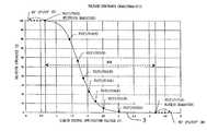
- FIG. 6is a view showing a gray level-luminance characteristic of a conventional liquid crystal display device of 8-bit (256 levels) display.
- reference numeral 7designates a gray level-luminance characteristic.
- FIG. 7is a view showing a liquid crystal application voltage-luminance characteristic of a conventional liquid crystal display device of 8-bit (256 levels) display.
- reference numeral 8designates the liquid crystal application voltage-luminance characteristic.
- symbol NURdesignates a normal use range.
- FIG. 4is based on the liquid crystal display device of the normally white mode in which a white display is carried out in a state where an effective voltage is not applied to the liquid crystal element.
- the liquid crystal application voltage (signal voltage) 1 or 2when the liquid crystal application voltage (signal voltage) 1 or 2 is changed, the liquid crystal element starts to respond as indicated by the luminance change 3 or 4 , and like the liquid crystal application voltage (signal voltage) 2 and the luminance change 4 , the larger the amount of change of the liquid crystal application voltage (signal voltage) is, the shorter the time until the response is completed is. That is, the response of the liquid crystal element between white and black is quick as compared with the response of the liquid crystal element between gray levels. Then, as shown in FIG.
- positive and negative reference voltagesof approximately 10 to 18 levels in total are normally inputted to a liquid crystal driving circuit, voltages between the respective reference voltages are divided by the liquid crystal driving circuit on the basis of the reference voltages, output voltages of 256 levels are generated in the respective polarities, and an output voltage corresponding to inputted data is selected and is outputted.
- Reference symbols V 0 to V 17 of the liquid crystal application voltage-luminance characteristic 8 of FIG. 7designate reference voltages inputted to the liquid crystal driving circuit in order to realize the gray level-luminance characteristic 7 of FIG. 6 .
- V 8 (P)/V 9 (N) corresponding to a white displayis set to a voltage at which the relative luminance becomes approximately 100%
- V 0 (P)/V 17 (N) corresponding to a black displayis set to a voltage at which a sufficient contrast ratio can be obtained.
- characters (P) and (N)mean (Positive) and (Negative), and express a positive reference voltage and a negative reference voltage, respectively.
- a voltage value which can be selected as a correction value of the liquid crystal application voltageis a white level one at the minimum, and there is a gray level in which the correction voltage is insufficient so that the speed of a liquid crystal response property can not be made high.
- blacka gray level which can be selected as a correction value of the liquid crystal application voltage
- the present inventionhas been made to solve the foregoing problem, and an object thereof is to provide a liquid crystal display device in which visibility at a time of display of moving pictures between gray levels is improved even in a case where a gray level change is slight.
- a liquid crystal display device including liquid crystal elements according to the present inventioncarries out a display corresponding to an inputted image signal, in which a liquid crystal driving circuit for supplying a voltage to each of the liquid crystal elements supplies a signal voltage corresponding to the inputted image signal and a correction voltage for speeding up a response speed of each of the liquid crystal elements prior to the signal voltage, a maximum value of the correction voltage is set higher than a maximum value of the signal voltage, and a minimum value of the correction voltage is set lower than a minimum value of the signal voltage.
- the liquid crystal display devicein which the maximum value of the correction voltage is set higher than the maximum value of the signal voltage, and the minimum value of the correction voltage is set lower than the minimum value of the signal voltage, even in the case where the signal voltage change is slight, whereby it is possible to speed up the response of each of the liquid crystal elements.
- a liquid crystal display device including liquid crystal elementscarries out a display corresponding to an inputted image signal, in which a liquid crystal driving circuit for supplying a voltage to each of the liquid crystal elements supplies a signal voltage corresponding to the inputted image signal and a correction voltage for speeding up a response speed of each of the liquid crystal elements prior to the signal voltage, and the liquid crystal driving circuit includes a first reference voltage used for supplying the signal voltage and a second reference voltage used for supplying the correction voltage, a maximum value of the second reference voltage is higher than a maximum value of the first reference voltage, and a minimum value of the second reference voltage is lower than a minimum value of the first reference voltage.
- the liquid crystal display devicein which the liquid crystal driving circuit includes the first reference voltage used for supplying the signal voltage and the second reference voltage used for supplying the correction voltage, the maximum value of the second reference voltage is higher than the maximum value of the first reference voltage, and the minimum value of the second reference voltage is lower than the minimum value of the first reference voltage, whereby even in the case where the signal voltage change is slight, it is possible to speed up the response of each of the liquid crystal elements.
- the liquid crystal display device of the present inventionhas a configuration, wherein the liquid crystal driving circuit includes a terminal to which the second reference voltage is inputted and a terminal to which a control signal to select one of the first reference voltage and the second reference voltage is inputted.
- the second reference voltagecan be selected when necessary and can be used.
- the liquid crystal display device of the present inventionhas a configuration, wherein the second reference voltage is supplied at a time when the signal voltage is changed to one of its maximum value and minimum value.
- the liquid crystal display device of the present inventionhas a configuration, wherein the second reference voltage is supplied which has such a value that when the signal voltage is changed to one of the maximum value and the minimum value, the luminance of each of liquid crystal elements corresponding to the signal voltage is not distorted.
- the second reference voltagedoes not have a bad influence on display quality.
- FIG. 1is a view showing a liquid crystal application voltage-luminance characteristic of a liquid crystal display device according to a first embodiment of the present invention.
- FIG. 2is a view for explaining an improvement in a gray level-luminance characteristic of a liquid crystal display device according to a second embodiment of the present invention.
- FIG. 3is a view showing a liquid crystal application voltage-luminance characteristic of the liquid crystal display device according to the second embodiment of the present invention.
- FIG. 4is a schematic view showing a relation between a liquid crystal application voltage (signal voltage) and a liquid crystal response (luminance change) in a conventional liquid crystal display device of a normally white mode.
- FIG. 5is a schematic view showing a relation between a liquid crystal application voltage and a liquid crystal response (luminance change) using a conventional Overdrive Method.
- FIG. 6is a view showing a gray level-luminance characteristic of a conventional liquid crystal display device of 8-bit display (256 levels).
- FIG. 7is a view showing a liquid crystal application voltage-luminance characteristic of a conventional liquid crystal display device of 8-bit display (256 levels).
- FIG. 1is a view showing a liquid crystal application voltage-luminance characteristic of a liquid crystal display device according to a first embodiment of the present invention.
- reference numeral 9designates a liquid crystal application voltage-luminance characteristic of each of liquid crystal elements constituting the liquid crystal display device.
- a reference voltage V 8 (P)/V 9 (N) corresponding to whiteis shifted to a low voltage side as indicated by V 8 ′(P)/V 9 ′(N).
- a reference voltage V 0 (P)/V 17 (N) corresponding to blackis shifted to a high voltage side as indicated by V 0 ′(P)/V 17 ′(N).
- characters (P) and (N)mean (Positive) and (Negative), and express a positive reference voltage and a negative reference voltage, respectively.
- the liquid crystal display devicewhile a liquid crystal application voltage (signal voltage) at which luminance corresponding to an inputted image signal can be obtained is supplied to each of the liquid crystal elements by a liquid crystal driving circuit, the shifted reference voltage as shown in FIG. 1 is used, and the liquid crystal driving circuit supplies a correction voltage to each of the liquid crystal elements prior to the supply of the liquid crystal application voltage (signal voltage) at which luminance corresponding to the inputted image signal can be obtained.
- the liquid crystal application voltagebecomes high unlike the prior art, and it becomes possible to speed up the liquid crystal response to luminance change toward the vicinity of white or black.
- an optimum level among the white dot markscan be selected from the relation between the luminance of the previous screen and the luminance of the present screen.
- symbol NUR in FIG. 1designates a normal use range.
- an existing liquid crystal driving driver ICcan be used, and even in the case where a luminance change is slight, the visibility of transition between different gray levels on moving pictures can be improved.
- a gray level-luminance characteristicwithout a difference in superiority and equivalent or almost equivalent to the prior art can be obtained, and further, the visibility at the time of display of moving pictures between a rather bright gray level and a brighter gray level or between a rather dark gray level and a darker gray level can be improved.
- FIG. 2is a view for explaining an improvement in a gray level-luminance characteristic of a liquid crystal display device according to a second embodiment of the present invention.
- reference numeral 10designates a gray level-luminance characteristic.
- FIG. 3is a view showing a liquid crystal application voltage-luminance characteristic of the liquid crystal display device according to the second embodiment of the present invention.
- symbol NURdesignates a normal use range.
- reference numeral 11designates a liquid crystal application voltage-luminance characteristic.
- the gray level-luminance characteristic in the vicinity of black and whiteis influenced by the shift and is slightly distorted like the gray level-luminance characteristic 10 of FIG. 2 .
- reference voltages for correction voltagesV A (P), V B (N), V C (P), V D (N) are provided as second reference voltages used for speeding up the response of liquid crystal element.
- FIG. 3shows the liquid crystal application voltage-luminance characteristic 11 in the second embodiment.
- a signal line driving circuitis provided with an input terminal of reference voltage for correction voltage and a control input terminal for indicating which of a conventional gray level voltage and the newly provided reference voltage for the correction voltage is selected as an output voltage.
- the voltage between V A /V B and V 8 /V 9is divided to enable selection of one of white dot marks.
- an optimum level among the white dot markscan be selected from the relation between the luminance of a previous screen and the luminance of a present screen. The same applies to the voltage between V C /V D and V 0 /V 17 at the black side.
- the second embodimentwithout changing the gray level-luminance characteristic, even in the case where a gray level change is slight, the visibility at the time of display of moving pictures between gray levels can be improved.
- the gray level-luminance characteristic 11without a difference in superiority and equivalent or almost equivalent to the prior art can be obtained, and further, the visibility at the time of display of moving pictures between a rather bright gray level and a brighter gray level or between a rather dark gray level and a darker gray level can be improved.
Landscapes
- Engineering & Computer Science (AREA)
- Chemical & Material Sciences (AREA)
- Crystallography & Structural Chemistry (AREA)
- Physics & Mathematics (AREA)
- Computer Hardware Design (AREA)
- General Physics & Mathematics (AREA)
- Theoretical Computer Science (AREA)
- Liquid Crystal Display Device Control (AREA)
- Control Of Indicators Other Than Cathode Ray Tubes (AREA)
- Liquid Crystal (AREA)
Abstract
Description
Claims (7)
Applications Claiming Priority (2)
| Application Number | Priority Date | Filing Date | Title |
|---|---|---|---|
| JPP2000-293407 | 2000-09-27 | ||
| JP2000293407AJP3511592B2 (en) | 2000-09-27 | 2000-09-27 | Liquid crystal display |
Publications (2)
| Publication Number | Publication Date |
|---|---|
| US20020057249A1 US20020057249A1 (en) | 2002-05-16 |
| US6876347B2true US6876347B2 (en) | 2005-04-05 |
Family
ID=18776210
Family Applications (1)
| Application Number | Title | Priority Date | Filing Date |
|---|---|---|---|
| US09/962,599Expired - LifetimeUS6876347B2 (en) | 2000-09-27 | 2001-09-26 | Liquid crystal display device |
Country Status (3)
| Country | Link |
|---|---|
| US (1) | US6876347B2 (en) |
| JP (1) | JP3511592B2 (en) |
| KR (1) | KR100550134B1 (en) |
Cited By (9)
| Publication number | Priority date | Publication date | Assignee | Title |
|---|---|---|---|---|
| US20030098874A1 (en)* | 2001-11-27 | 2003-05-29 | Akira Tobiya | Image display system and image display device |
| US20040189580A1 (en)* | 2003-03-31 | 2004-09-30 | Fujitsu Display Technologies Corporation | Liquid crystal display device |
| US20050122300A1 (en)* | 2003-11-07 | 2005-06-09 | Masami Makuuchi | Semiconductor device and testing method thereof |
| US20050184948A1 (en)* | 2004-02-20 | 2005-08-25 | Genesis Microchip Inc. | Extended overdrive table and methods of use thereof for enhancing the appearance of motion on an LCD panel |
| US20070120791A1 (en)* | 2005-11-28 | 2007-05-31 | Nec Lcd Technologies, Ltd | Driving circuit and driving method for liquid crystal display panel |
| US20080018734A1 (en)* | 2006-07-20 | 2008-01-24 | Pentax Corporation | Endoscope System |
| US20080079674A1 (en)* | 2006-07-05 | 2008-04-03 | Yoshihisa Ooishi | Display device and method for driving the same |
| US7382349B1 (en)* | 2004-09-30 | 2008-06-03 | National Semiconductor Corporation | Methods and systems for determining display overdrive signals |
| US20080198223A1 (en)* | 2007-02-19 | 2008-08-21 | Pentax Corporation | Electronic endoscope system and processor for electronic endoscope |
Families Citing this family (14)
| Publication number | Priority date | Publication date | Assignee | Title |
|---|---|---|---|---|
| WO2004015670A1 (en)* | 2002-07-29 | 2004-02-19 | Koninklijke Philips Electronics N.V. | Driving of a liquid crystal display |
| TWI285868B (en)* | 2003-01-20 | 2007-08-21 | Ind Tech Res Inst | Method and apparatus to enhance response time of display |
| EP1460612A3 (en)* | 2003-03-19 | 2006-11-15 | Sharp Kabushiki Kaisha | Driving method of liquid crystal display apparatus, driving apparatus of liquid crystal display apparatus, and program thereof |
| KR100945580B1 (en)* | 2003-06-10 | 2010-03-08 | 삼성전자주식회사 | Driving apparatus and method of liquid crystal display |
| CN100466056C (en)* | 2003-06-11 | 2009-03-04 | 友达光电股份有限公司 | scanning method of liquid crystal display |
| JP4191136B2 (en) | 2004-03-15 | 2008-12-03 | シャープ株式会社 | Liquid crystal display device and driving method thereof |
| JP2006003867A (en)* | 2004-05-20 | 2006-01-05 | Seiko Epson Corp | Image correction amount detection device, drive circuit for electro-optical device, electro-optical device, and electronic apparatus |
| US7978164B2 (en) | 2005-03-30 | 2011-07-12 | Sharp Kabushiki Kaisha | Liquid crystal display device |
| JP2007033864A (en)* | 2005-07-27 | 2007-02-08 | Mitsubishi Electric Corp | Image processing circuit and image processing method |
| KR101253243B1 (en)* | 2005-08-31 | 2013-04-16 | 엘지디스플레이 주식회사 | Liquid crystal display device and method of driving the same |
| CN101806656B (en)* | 2010-03-08 | 2011-09-07 | 东南大学 | Luminosity response characteristics measuring instrument of notebook computer liquid crystal display screen |
| WO2012081212A1 (en)* | 2010-12-17 | 2012-06-21 | シャープ株式会社 | Drive device for display device, drive method, and display device system |
| CN103064203A (en)* | 2011-10-20 | 2013-04-24 | 四川长虹电器股份有限公司 | Response time measuring device and response time measuring method of liquid crystal display (LCD) panel |
| CN110085177A (en)* | 2018-01-25 | 2019-08-02 | 奇景光电股份有限公司 | Display device and overdrive method |
Citations (8)
| Publication number | Priority date | Publication date | Assignee | Title |
|---|---|---|---|---|
| JPS60247378A (en) | 1984-05-22 | 1985-12-07 | Casio Comput Co Ltd | A/d converting circuit of video signal |
| JPH0627901A (en) | 1992-07-09 | 1994-02-04 | Fujitsu Ltd | Liquid crystal display device |
| US5657041A (en)* | 1994-06-03 | 1997-08-12 | Samsung Display Devices Co., Ltd. | Method for driving a matrix liquid crystal display panel with reduced cross-talk and improved brightness ratio |
| US5920298A (en)* | 1996-12-19 | 1999-07-06 | Colorado Microdisplay, Inc. | Display system having common electrode modulation |
| US6144353A (en)* | 1996-12-19 | 2000-11-07 | Colorado Microdisplay, Inc. | Display system having electrode modulation to alter a state of an electro-optic layer |
| US6232942B1 (en)* | 1995-08-28 | 2001-05-15 | Citizen Watch Co., Ltd. | Liquid crystal display device |
| US6304304B1 (en)* | 1997-11-20 | 2001-10-16 | Sanyo Electric Co., Ltd. | Liquid crystal display having an off driving voltage greater than either zero or an optical characteristics changing voltage |
| US20010040546A1 (en)* | 1998-12-08 | 2001-11-15 | Fujitsu Limited | Liquid crystal display device and its drive method |
Family Cites Families (7)
| Publication number | Priority date | Publication date | Assignee | Title |
|---|---|---|---|---|
| EP0927416A1 (en)* | 1997-07-22 | 1999-07-07 | Koninklijke Philips Electronics N.V. | Display device |
| JPH11296150A (en)* | 1998-04-10 | 1999-10-29 | Masaya Okita | High-speed driving method for liquid crystal |
| JP3483245B2 (en)* | 1999-03-10 | 2004-01-06 | シャープ株式会社 | Driving method of liquid crystal display device |
| JP3534389B2 (en)* | 1999-03-10 | 2004-06-07 | シャープ株式会社 | Liquid crystal display device and driving method thereof |
| US6927825B1 (en)* | 1999-05-14 | 2005-08-09 | Sanyo Electric Co., Ltd. | Liquid crystal display using liquid crystal with bend alignment and driving method thereof |
| JP2001209345A (en) | 2000-01-24 | 2001-08-03 | Canon Inc | Driving method of display device |
| KR100660532B1 (en)* | 2000-03-07 | 2006-12-22 | 삼성전자주식회사 | Flat panel display device and gray level voltage generation method thereof |
- 2000
- 2000-09-27JPJP2000293407Apatent/JP3511592B2/ennot_activeExpired - Fee Related
- 2001
- 2001-09-24KRKR1020010058967Apatent/KR100550134B1/ennot_activeExpired - Fee Related
- 2001-09-26USUS09/962,599patent/US6876347B2/ennot_activeExpired - Lifetime
Patent Citations (8)
| Publication number | Priority date | Publication date | Assignee | Title |
|---|---|---|---|---|
| JPS60247378A (en) | 1984-05-22 | 1985-12-07 | Casio Comput Co Ltd | A/d converting circuit of video signal |
| JPH0627901A (en) | 1992-07-09 | 1994-02-04 | Fujitsu Ltd | Liquid crystal display device |
| US5657041A (en)* | 1994-06-03 | 1997-08-12 | Samsung Display Devices Co., Ltd. | Method for driving a matrix liquid crystal display panel with reduced cross-talk and improved brightness ratio |
| US6232942B1 (en)* | 1995-08-28 | 2001-05-15 | Citizen Watch Co., Ltd. | Liquid crystal display device |
| US5920298A (en)* | 1996-12-19 | 1999-07-06 | Colorado Microdisplay, Inc. | Display system having common electrode modulation |
| US6144353A (en)* | 1996-12-19 | 2000-11-07 | Colorado Microdisplay, Inc. | Display system having electrode modulation to alter a state of an electro-optic layer |
| US6304304B1 (en)* | 1997-11-20 | 2001-10-16 | Sanyo Electric Co., Ltd. | Liquid crystal display having an off driving voltage greater than either zero or an optical characteristics changing voltage |
| US20010040546A1 (en)* | 1998-12-08 | 2001-11-15 | Fujitsu Limited | Liquid crystal display device and its drive method |
Cited By (14)
| Publication number | Priority date | Publication date | Assignee | Title |
|---|---|---|---|---|
| US20030098874A1 (en)* | 2001-11-27 | 2003-05-29 | Akira Tobiya | Image display system and image display device |
| US8773476B2 (en)* | 2001-11-27 | 2014-07-08 | NEC—Mitsubishi Electric Visual Systems Corporation | Image display system and image display device |
| US20040189580A1 (en)* | 2003-03-31 | 2004-09-30 | Fujitsu Display Technologies Corporation | Liquid crystal display device |
| US7474290B2 (en)* | 2003-11-07 | 2009-01-06 | Renesas Technology Corp. | Semiconductor device and testing method thereof |
| US20050122300A1 (en)* | 2003-11-07 | 2005-06-09 | Masami Makuuchi | Semiconductor device and testing method thereof |
| US20050184948A1 (en)* | 2004-02-20 | 2005-08-25 | Genesis Microchip Inc. | Extended overdrive table and methods of use thereof for enhancing the appearance of motion on an LCD panel |
| US7683868B2 (en)* | 2004-02-20 | 2010-03-23 | Genesis Microchip Inc. | Extended overdrive table and methods of use thereof for enhancing the appearance of motion on an LCD panel |
| US7382349B1 (en)* | 2004-09-30 | 2008-06-03 | National Semiconductor Corporation | Methods and systems for determining display overdrive signals |
| US7724226B2 (en)* | 2005-11-28 | 2010-05-25 | Nec Lcd Technologies, Ltd. | Driving circuit and driving method for liquid crystal display panel |
| US20070120791A1 (en)* | 2005-11-28 | 2007-05-31 | Nec Lcd Technologies, Ltd | Driving circuit and driving method for liquid crystal display panel |
| US20080079674A1 (en)* | 2006-07-05 | 2008-04-03 | Yoshihisa Ooishi | Display device and method for driving the same |
| US20080018734A1 (en)* | 2006-07-20 | 2008-01-24 | Pentax Corporation | Endoscope System |
| US20080198223A1 (en)* | 2007-02-19 | 2008-08-21 | Pentax Corporation | Electronic endoscope system and processor for electronic endoscope |
| US8102415B2 (en)* | 2007-02-19 | 2012-01-24 | Hoya Corporation | Electronic endoscope system and processor for electronic endoscope |
Also Published As
| Publication number | Publication date |
|---|---|
| JP3511592B2 (en) | 2004-03-29 |
| KR20020028782A (en) | 2002-04-17 |
| US20020057249A1 (en) | 2002-05-16 |
| KR100550134B1 (en) | 2006-02-08 |
| JP2002107694A (en) | 2002-04-10 |
Similar Documents
| Publication | Publication Date | Title |
|---|---|---|
| US6876347B2 (en) | Liquid crystal display device | |
| KR100515900B1 (en) | Liquid crystal display device | |
| US7034786B2 (en) | Color-correction method and apparatus for liquid crystal display | |
| EP1564714B1 (en) | Display device, liquid crytal monitor, liquid crystal television receiver, and display method | |
| KR100542767B1 (en) | Driving Method and Driving Device of Liquid Crystal Display | |
| TWI328209B (en) | Display device | |
| JPH11175027A (en) | Liquid crystal drive circuit and liquid crystal display device | |
| KR100859391B1 (en) | Display device | |
| KR20020059253A (en) | Controller circuit for liquid crystal matrix display devices | |
| US7023414B2 (en) | Method and apparatus for driving liquid crystal display | |
| US20120249619A1 (en) | Display device | |
| US20060007207A1 (en) | Liquid crystal display device and method of driving liquid crystal display device | |
| KR100701515B1 (en) | A method of driving a display device, a display device, and a computer readable recording medium having recorded thereon a computer program | |
| US20090267881A1 (en) | Liquid crystal display | |
| KR100783697B1 (en) | Liquid Crystal Display With Moving Image Correction Function And Driving Device And Method thereof | |
| US7649575B2 (en) | Liquid crystal display device with improved response speed | |
| US7443369B2 (en) | Liquid crystal display device and an optimum gradation voltage setting apparatus thereof | |
| JP2009058684A (en) | Liquid crystal display | |
| KR100806908B1 (en) | Driving device of liquid crystal display | |
| KR100864978B1 (en) | Gamma Compensation Method and Apparatus for LCD | |
| KR100788387B1 (en) | Gamma voltage setting method and device | |
| KR20050055158A (en) | Liquid crystal display and driving method thereof | |
| JPH09244591A (en) | Driving method of liquid crystal display device | |
| KR20100030208A (en) | An apparatus for displaying an image | |
| KR20060037516A (en) | LCD Display |
Legal Events
| Date | Code | Title | Description |
|---|---|---|---|
| AS | Assignment | Owner name:KABUSHIKI KAISHA ADVANCED DISPLAY, JAPAN Free format text:ASSIGNMENT OF ASSIGNORS INTEREST;ASSIGNORS:TASHIRO, TOMOHIRO;TAKAHASHI, SEIKI;MIYAKE, SHIRO;REEL/FRAME:012505/0900;SIGNING DATES FROM 20011207 TO 20011211 | |
| FEPP | Fee payment procedure | Free format text:PAYOR NUMBER ASSIGNED (ORIGINAL EVENT CODE: ASPN); ENTITY STATUS OF PATENT OWNER: LARGE ENTITY | |
| STCF | Information on status: patent grant | Free format text:PATENTED CASE | |
| AS | Assignment | Owner name:MITSUBISHI ELECTRIC CORPORATION, JAPAN Free format text:ASSIGNMENT OF ASSIGNORS INTEREST;ASSIGNOR:KABUSHIKI KAISHA ADVANCED DISPLAY;REEL/FRAME:020156/0143 Effective date:20071111 | |
| FPAY | Fee payment | Year of fee payment:4 | |
| FPAY | Fee payment | Year of fee payment:8 | |
| FPAY | Fee payment | Year of fee payment:12 | |
| AS | Assignment | Owner name:TRIVALE TECHNOLOGIES, CALIFORNIA Free format text:ASSIGNMENT OF ASSIGNORS INTEREST;ASSIGNOR:MITSUBISHI ELECTRIC CORPORATION;REEL/FRAME:057651/0234 Effective date:20210205 |