US6875686B2 - Method for fabricating a structure of interconnections comprising an electric insulation including air or vacuum gaps - Google Patents
Method for fabricating a structure of interconnections comprising an electric insulation including air or vacuum gapsDownload PDFInfo
- Publication number
- US6875686B2 US6875686B2US10/168,949US16894902AUS6875686B2US 6875686 B2US6875686 B2US 6875686B2US 16894902 AUS16894902 AUS 16894902AUS 6875686 B2US6875686 B2US 6875686B2
- Authority
- US
- United States
- Prior art keywords
- level
- electric
- conductors
- electric conductors
- layer
- Prior art date
- Legal status (The legal status is an assumption and is not a legal conclusion. Google has not performed a legal analysis and makes no representation as to the accuracy of the status listed.)
- Expired - Lifetime, expires
Links
Images


Classifications
- H—ELECTRICITY
- H01—ELECTRIC ELEMENTS
- H01L—SEMICONDUCTOR DEVICES NOT COVERED BY CLASS H10
- H01L21/00—Processes or apparatus adapted for the manufacture or treatment of semiconductor or solid state devices or of parts thereof
- H01L21/70—Manufacture or treatment of devices consisting of a plurality of solid state components formed in or on a common substrate or of parts thereof; Manufacture of integrated circuit devices or of parts thereof
- H01L21/71—Manufacture of specific parts of devices defined in group H01L21/70
- H01L21/768—Applying interconnections to be used for carrying current between separate components within a device comprising conductors and dielectrics
- H01L21/76801—Applying interconnections to be used for carrying current between separate components within a device comprising conductors and dielectrics characterised by the formation and the after-treatment of the dielectrics, e.g. smoothing
- H01L21/7682—Applying interconnections to be used for carrying current between separate components within a device comprising conductors and dielectrics characterised by the formation and the after-treatment of the dielectrics, e.g. smoothing the dielectric comprising air gaps
Definitions
- the present inventionconcerns a method for fabricating a structure of damascene type interconnections on a semiconductor device.
- the structure of interconnectionsincludes an electric insulation associating some low permittivity material and some air or vacuum gaps.
- aluminiumtends to be replaced by copper and the classic dielectric materials used such as SiO 2 , Si x N y , SiO x N y tend to be replaced by materials of the type that are doped with fluorine (FSG, for example), methylsilsesquioxane (MSQ), hydrogen silsesquioxane (HSQ), organic materials (ECB, Silk, Flare, PAE, etc . . . ), porous materials (NanoGlass, for example), etc . . .
- FSGfluorine
- MSQmethylsilsesquioxane
- HSQhydrogen silsesquioxane
- organic materialsECB, Silk, Flare, PAE, etc . . .
- porous materialsNanoGlass, for example
- the latest limitis the use of vacuum or of air. It is the control of this latest kind of insulation which currently poses a problem.
- the document EP-A-0 834 916also publishes the use of air gaps to realize a structure for enhanced performance interconnections (damascene structure).
- the technique published by this documentmay not however be used when the structure includes expanded contacts, that is to say, interconnections in which the metal contacts (or vias) linking an n-level metal to the higher level n+1 metal may be of a larger size than the n-level metal lines or positioned overlapping the n-level metal.
- the air or vacuum gapsare formed before etching the holes which will allow you to connect the n-level metal to the n+1 level metal. Therefore, these holes will emerge over the gaps, which makes it impossible for them to be filled by a metal afterwards.
- FIG. 1Ashows a simple damascene structure, already familiar in the state of the art, formed on one side 2 of a semiconductor substrate 1 .
- the side 2is covered by a first layer of dielectric material 3 , with the latter being covered by a second layer of dielectric material 4 meant to house copper lines 5 .
- the realization methodleaves gaps 6 in place that are meant to trap the air.
- a third layer of dielectric material 7is deposited on the structure allowing some small-sized gaps 6 to remain. This is shown in FIG. 1 B.
- FIG. 1Cshows the structure after some holes 8 have been made in the dielectric material layer 7 for housing the vias, which turn out to be expanded contacts.
- the holes 8pose a problem due to the fact that they finish above the gaps. Their filling for producing the expanded contacts, especially, poses a problem.
- Document EP-A-0 834 916also publishes the method for producing an electric insulation using some dielectric materials with low permittivity (less than 2.7) for damascene type interconnection structures.
- the interconnectionsare first made with an insulator with a permittivity lower than 3.5, which is then removed and replaced by an insulator with a permittivity lower than 2.7 (chosen from amongst HSQ, BCB, a polymide and PAE).
- This realization methodposes some serious problems of planarisation: good planarisation in the regions with heavy density of metal, bad planarisation on the insulated metal lines. Furthermore, this method means losing all the advantages offered by the damascene technology.
- the present inventionhas been designed to solve the problems described above. It allows electric insulations to be to made for metal interconnections realized in damascene technology covering a combination of gaps (trapping air or a vacuum), dielectric materials with low permittivity (less than 3) and SiO 2 , Si x N y , SiO x N y and SiOF type materials. These electric insulations are compatible with metal contacts linking an n level metal to the n+1 level metal, and these metal contacts may be of a larger size than the n level metal lines or positioned overlapping the n level metal and the adjacent dielectric. This procedure also allows for perfect planarisation of the interconnections.
- the purpose of the inventionis a method for fabricating a damascene type structure of interconnections on a semiconductor device, with the interconnections structure including at least a first level of conductors covered by a second level of conductors aimed at ensuring electrical links with the conductors on the first level, with the interconnections structure also including an electric insulation associating some material with low permittivity and some air or vacuum gaps, characterised by the fact that it includes the following steps:
- first level of conductors in a first electric insulating layer and of the second level of conductors in a second electric insulating layerwith the conductors in the first level being arranged with a pre-determined spacing in order to allow, in a later step, the formation of air or vacuum gaps between the conductors in the first level
- the electric insulation layersmay be layers made of a material chosen between SiO 2 and SiOF.
- the methodincludes the deposit of an interface layer made of an insulating material on the semi-conductor device before the formation of the first level of conductors, and the deposit of an interface layer on the first level of conductors before the formation of the second level of conductors.
- the insulating material in the interface layer deposited on the semi-conductor devicemay be chosen from amongst Si x N y , SiO x N y and SiC.
- the interface layer separating the first level of conductors from the second level of conductorsmay be made of a material selected from amongst Si x N y , SiO x N y and SiC.
- the methodincludes, after the elimination of the second electric insulating layer, the complete elimination of the interface layer separating the first level of conductors from the second level of conductors and the complete elimination of the first electric insulating layer.
- the methodincludes, after the elimination of the second electric insulating layer, the deposit of a layer of resin on the interface layer deposited on the first level of conductors, the formation of a mask made up by the layer of resin with a view to performing the partial elimination of the of the first electric insulating layer, the elimination of the part of the interface layer deposited on the first level of conductors and not masked by the resin mask, then the step for the elimination of the first electric insulating layer may be undertaken.
- the conductors in the first level of conductors and the conductors in the second level of conductorsare made of copper or based on copper.
- FIGS. 1A to 1 Care cross-section views of a damascene type structure of interconnections, in accordance with the state of the art as it is known, during the course of its realization,
- FIGS. 2A to 2 Fare cross-section views of a damascene type structure of interconnections during the course of its realization, in accordance with a first embodiment of the invention
- FIGS. 3A to 3 Dare cross-section views of a damascene type structure of interconnections during the course of its realization, in accordance with a second embodiment of the invention.
- FIGS. 4A to 4 Care cross-section views of a damascene type structure of interconnections with expanded contacts and during the course of its realization, in accordance with the first embodiment of the invention.
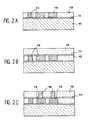
- FIGS. 2A to 2 Fillustrate a first mode for implementing the invention based on a silicon substrate.
- an interface layer 14for example, made of Si x N y or SiO x N y or SiC, is deposited on the first electric insulating layer 12 integrating the conducting lines 13 .
- a second electric insulating layer 15is deposited, for example, made of SiO 2 or SiOF.
- conducting vias 16are then formed across the second electric insulating layer 15 and the interface layer 14 .
- the conducting vias 16ensure an electric link with the conducting lines 13 .
- the conducting lines and the conducting viasmay include some barrier layers, for example, made of TiN, Ta, TaN, W or WN.
- the second electric insulating layer, 15 , the interface layer 14 and the first electric insulating layer 12are eliminated.
- the structure shown in FIG. 2Dis obtained.
- a dielectric material 17 with low permittivityis deposited on this structure, a material known as a low-k (permittivity less than 3): for example, a polymer, SiOC, a porous dielectric material (for example, a material from the Nanoglass trademark), HSQ.
- the material 17may be deposited by spreading or by chemical vapour deposition (CVD). It may involve, in this case, material with a high level of viscosity, a polymer with a long monomer chain. Some adapted deposit methods may also be used (PECVD, etc . . . ), which leave gaps in the small-sized spaces between the metals.
- FIG. 2Eshows this step of the method and especially shows the presence of gaps 18 between the conducting lines 13 . This Figure also shows that the conducting vias 16 are covered by the dielectric material 17 .
- CMPchemical-mechanical polishing process
- FIGS. 3A to 3 Dillustrate a second embodiment of the invention based on a silicon substrate.
- FIG. 3Ashows the structure obtained after the elimination of the second electric insulating layer.
- the interface layer located between the two layers of electric insulationcould also be eliminated.
- the substrate 20supports an interface layer 21 , and the latter itself is covered by the first electric insulating layer 22 integrating the conducting lines 23 .
- the interface layer 24covers this first level of conductors, with the conducting vias 26 thereby ensuring the electric link with some conducting lines 23 .
- a layer of photosensitive resinis then deposited on the structure to form, by lithography, a mask 29 protecting the areas where the spaces between the lines 23 are large, for example, over 0.5 ⁇ m (see FIG. 3 B).
- the areas in the interface layer 24 and the first electric insulating layer 22 not protected by the resin mask 29are eliminated. These areas correspond to the places in the structure where the conducting lines 23 are arranged closely (for example, with a spacing of less than 0.5 ⁇ m). The result obtained is illustrated in FIG. 3 C.
- a dielectric material 27 with low permittivity and with a low capacity for fillingis deposited on this structure. Then, as shown in FIG. 3D , some gaps 28 are formed between the conducting lines 26 that are very slightly separated.
- the conducting vias 26which were initially covered by the dielectric material 27 whose upper level is shown with dot and dash lines, are exposed following a method for etching or chemical and mechanical polishing the excess dielectric material 27 .
- FIGS. 4A to 4 Cillustrate the production of a damascene type structure of interconnections with expanded contacts, according to the first embodiment of the invention.
- the first steps in the realization methodare identical to those illustrated in FIGS. 2A to 2 C, with the exception of the position of the vias.
- the structure obtained in this stepis the one shown in FIG. 4 A.
- the substrate 30supports an interface layer 31 , the latter itself is covered by the first electric insulating layer 32 integrating the conducting lines 33 .
- the interface layer 34covers this first level of conductors and supports the second electric insulating layer 35 integrating the conductor vias 36 thereby ensuring the electric link to the conductor lines 33 .
- the second electric insulating layer 35 , the interface layer 34 and the first electric insulating layer 32are eliminated.
- the structure shown in FIG. 4Bis obtained.
- a dielectric material 37 with low permittivity and a low capacity for fillingis obtained. Then, as shown in FIG. 4C , some gaps 38 are formed between the conductor lines 33 which are arranged very closely together.
- the expanded contacts 36initially covered by the dielectric material 37 whose upper level is represented by dot and dash lines, are exposed following an etching or chemical and mechanical polishing process to remove the excess dielectric material 37 .
- the inventionallows structures with expanded contacts to be produced, since the formation of the gaps is performed after the production of the vias.
- the inventionallows:
- insulation barriers between the metalsincluding both vacuum or air, dielectric materials with low permittivity (less than 3) and mineral type dielectric materials (SiO x , Si x N y or SiO x N y , SiOF, . . . );
Landscapes
- Engineering & Computer Science (AREA)
- Physics & Mathematics (AREA)
- Condensed Matter Physics & Semiconductors (AREA)
- General Physics & Mathematics (AREA)
- Manufacturing & Machinery (AREA)
- Computer Hardware Design (AREA)
- Microelectronics & Electronic Packaging (AREA)
- Power Engineering (AREA)
- Internal Circuitry In Semiconductor Integrated Circuit Devices (AREA)
Abstract
Description
Claims (10)
Applications Claiming Priority (2)
| Application Number | Priority Date | Filing Date | Title |
|---|---|---|---|
| FR9916637AFR2803438B1 (en) | 1999-12-29 | 1999-12-29 | METHOD FOR PRODUCING AN INTERCONNECTION STRUCTURE INCLUDING ELECTRICAL INSULATION INCLUDING AIR OR VACUUM CAVITES |
| PCT/FR2000/003713WO2001050524A1 (en) | 1999-12-29 | 2000-12-28 | Interconnection structure with insulation comprising cavities |
Publications (2)
| Publication Number | Publication Date |
|---|---|
| US20030077893A1 US20030077893A1 (en) | 2003-04-24 |
| US6875686B2true US6875686B2 (en) | 2005-04-05 |
Family
ID=9553954
Family Applications (1)
| Application Number | Title | Priority Date | Filing Date |
|---|---|---|---|
| US10/168,949Expired - LifetimeUS6875686B2 (en) | 1999-12-29 | 2000-12-28 | Method for fabricating a structure of interconnections comprising an electric insulation including air or vacuum gaps |
Country Status (4)
| Country | Link |
|---|---|
| US (1) | US6875686B2 (en) |
| EP (1) | EP1243024B1 (en) |
| FR (1) | FR2803438B1 (en) |
| WO (1) | WO2001050524A1 (en) |
Cited By (4)
| Publication number | Priority date | Publication date | Assignee | Title |
|---|---|---|---|---|
| US20060281298A1 (en)* | 2005-06-08 | 2006-12-14 | Hitachi, Ltd. | Semiconductor device and manufacturing method of the same |
| US20080122106A1 (en)* | 2006-09-11 | 2008-05-29 | International Business Machines | Method to generate airgaps with a template first scheme and a self aligned blockout mask |
| US20090068840A1 (en)* | 2007-08-31 | 2009-03-12 | Gaku Minamihaba | Polishing liquid and method for manufacturing semiconductor device |
| US20090263920A1 (en)* | 2006-04-05 | 2009-10-22 | Commissariat A L'energie Atomique | Protection of cavities opening onto a face of a microstructured element |
Families Citing this family (12)
| Publication number | Priority date | Publication date | Assignee | Title |
|---|---|---|---|---|
| US7042095B2 (en)* | 2002-03-29 | 2006-05-09 | Renesas Technology Corp. | Semiconductor device including an interconnect having copper as a main component |
| US6949456B2 (en)* | 2002-10-31 | 2005-09-27 | Asm Japan K.K. | Method for manufacturing semiconductor device having porous structure with air-gaps |
| US6812150B2 (en)* | 2002-12-26 | 2004-11-02 | Micron Technology, Inc. | Methods for making semiconductor device structures with capacitor containers and contact apertures having increased aspect ratios |
| US20060183317A1 (en)* | 2003-03-14 | 2006-08-17 | Junji Noguchi | Semiconductor device and a method of manufacturing the same |
| JP4918778B2 (en)* | 2005-11-16 | 2012-04-18 | 株式会社日立製作所 | Manufacturing method of semiconductor integrated circuit device |
| JP5396065B2 (en)* | 2008-10-28 | 2014-01-22 | 株式会社日立製作所 | Manufacturing method of semiconductor device |
| US8456009B2 (en) | 2010-02-18 | 2013-06-04 | Taiwan Semiconductor Manufacturing Company, Ltd. | Semiconductor structure having an air-gap region and a method of manufacturing the same |
| US8575000B2 (en) | 2011-07-19 | 2013-11-05 | SanDisk Technologies, Inc. | Copper interconnects separated by air gaps and method of making thereof |
| KR102003881B1 (en)* | 2013-02-13 | 2019-10-17 | 삼성전자주식회사 | Semiconductor deivces and methods of fabricating the same |
| KR102190654B1 (en)* | 2014-04-07 | 2020-12-15 | 삼성전자주식회사 | Semiconductor device and method of fabricating the same |
| US9401304B2 (en)* | 2014-04-24 | 2016-07-26 | Sandisk Technologies Llc | Patterning method for low-k inter-metal dielectrics and associated semiconductor device |
| US10361117B2 (en)* | 2017-12-11 | 2019-07-23 | International Business Machines Corporation | Selective ILD deposition for fully aligned via with airgap |
Citations (6)
| Publication number | Priority date | Publication date | Assignee | Title |
|---|---|---|---|---|
| US5559055A (en) | 1994-12-21 | 1996-09-24 | Advanced Micro Devices, Inc. | Method of decreased interlayer dielectric constant in a multilayer interconnect structure to increase device speed performance |
| JPH10233449A (en) | 1997-02-20 | 1998-09-02 | Nec Corp | Manufacture of semiconductor device |
| GB2330001A (en) | 1997-10-06 | 1999-04-07 | United Microelectronics Corp | Multilevel interconnect with air dielectric |
| US5953626A (en) | 1996-06-05 | 1999-09-14 | Advanced Micro Devices, Inc. | Dissolvable dielectric method |
| US6071805A (en)* | 1999-01-25 | 2000-06-06 | Chartered Semiconductor Manufacturing, Ltd. | Air gap formation for high speed IC processing |
| US6165890A (en)* | 1997-01-21 | 2000-12-26 | Georgia Tech Research Corporation | Fabrication of a semiconductor device with air gaps for ultra-low capacitance interconnections |
Family Cites Families (2)
| Publication number | Priority date | Publication date | Assignee | Title |
|---|---|---|---|---|
| US5602423A (en)* | 1994-11-01 | 1997-02-11 | Texas Instruments Incorporated | Damascene conductors with embedded pillars |
| JPH09306988A (en)* | 1996-03-13 | 1997-11-28 | Sony Corp | Method of forming multilayer wiring |
- 1999
- 1999-12-29FRFR9916637Apatent/FR2803438B1/ennot_activeExpired - Fee Related
- 2000
- 2000-12-28EPEP00993755Apatent/EP1243024B1/ennot_activeExpired - Lifetime
- 2000-12-28WOPCT/FR2000/003713patent/WO2001050524A1/enactiveApplication Filing
- 2000-12-28USUS10/168,949patent/US6875686B2/ennot_activeExpired - Lifetime
Patent Citations (7)
| Publication number | Priority date | Publication date | Assignee | Title |
|---|---|---|---|---|
| US5559055A (en) | 1994-12-21 | 1996-09-24 | Advanced Micro Devices, Inc. | Method of decreased interlayer dielectric constant in a multilayer interconnect structure to increase device speed performance |
| US5953626A (en) | 1996-06-05 | 1999-09-14 | Advanced Micro Devices, Inc. | Dissolvable dielectric method |
| US6165890A (en)* | 1997-01-21 | 2000-12-26 | Georgia Tech Research Corporation | Fabrication of a semiconductor device with air gaps for ultra-low capacitance interconnections |
| JPH10233449A (en) | 1997-02-20 | 1998-09-02 | Nec Corp | Manufacture of semiconductor device |
| GB2330001A (en) | 1997-10-06 | 1999-04-07 | United Microelectronics Corp | Multilevel interconnect with air dielectric |
| FR2770028A1 (en) | 1997-10-06 | 1999-04-23 | United Microelectronics Corp | Multilevel interconnect structure for high density integrated circuit devices, integrated circuit memories |
| US6071805A (en)* | 1999-01-25 | 2000-06-06 | Chartered Semiconductor Manufacturing, Ltd. | Air gap formation for high speed IC processing |
Cited By (13)
| Publication number | Priority date | Publication date | Assignee | Title |
|---|---|---|---|---|
| US20060281298A1 (en)* | 2005-06-08 | 2006-12-14 | Hitachi, Ltd. | Semiconductor device and manufacturing method of the same |
| US8586447B2 (en) | 2005-06-08 | 2013-11-19 | Hitachi, Ltd. | Semiconductor device and manufacturing method of the same |
| US7501347B2 (en)* | 2005-06-08 | 2009-03-10 | Hitachi, Ltd. | Semiconductor device and manufacturing method of the same |
| US8247902B2 (en) | 2005-06-08 | 2012-08-21 | Hitachi, Ltd. | Semiconductor device and manufacturing method of the same |
| US20090142919A1 (en)* | 2005-06-08 | 2009-06-04 | Hitachi, Ltd. | Semiconductor device and manufacturing method of the same |
| US7911055B2 (en)* | 2005-06-08 | 2011-03-22 | Hitachi, Ltd. | Semiconductor device and manufacturing method of the same |
| US20110140275A1 (en)* | 2005-06-08 | 2011-06-16 | Hitachi, Ltd. | Semiconductor device and manufacturing method of the same |
| US20090263920A1 (en)* | 2006-04-05 | 2009-10-22 | Commissariat A L'energie Atomique | Protection of cavities opening onto a face of a microstructured element |
| US8153503B2 (en)* | 2006-04-05 | 2012-04-10 | Commissariat A L'energie Atomique | Protection of cavities opening onto a face of a microstructured element |
| US20110163446A1 (en)* | 2006-09-11 | 2011-07-07 | International Business Machines Corporation | Method to generate airgaps with a template first scheme and a self aligned blockout mask and structure |
| US7863150B2 (en)* | 2006-09-11 | 2011-01-04 | International Business Machines Corporation | Method to generate airgaps with a template first scheme and a self aligned blockout mask |
| US20080122106A1 (en)* | 2006-09-11 | 2008-05-29 | International Business Machines | Method to generate airgaps with a template first scheme and a self aligned blockout mask |
| US20090068840A1 (en)* | 2007-08-31 | 2009-03-12 | Gaku Minamihaba | Polishing liquid and method for manufacturing semiconductor device |
Also Published As
| Publication number | Publication date |
|---|---|
| FR2803438B1 (en) | 2002-02-08 |
| WO2001050524A1 (en) | 2001-07-12 |
| EP1243024A1 (en) | 2002-09-25 |
| EP1243024B1 (en) | 2011-06-08 |
| FR2803438A1 (en) | 2001-07-06 |
| US20030077893A1 (en) | 2003-04-24 |
Similar Documents
| Publication | Publication Date | Title |
|---|---|---|
| US6787911B1 (en) | Interconnect with low dielectric constant insulators for semiconductor integrated circuit manufacturing | |
| US6037664A (en) | Dual damascene interconnect structure using low dielectric constant material for an inter-level dielectric layer | |
| US7135398B2 (en) | Reliable low-k interconnect structure with hybrid dielectric | |
| US6177329B1 (en) | Integrated circuit structures having gas pockets and method for forming integrated circuit structures having gas pockets | |
| US7285474B2 (en) | Air-gap insulated interconnections | |
| CN101390203B (en) | Interconnect structure and manufacturing method thereof | |
| KR100497580B1 (en) | Interconnect structures containing stress adjustment cap layer | |
| US6893959B2 (en) | Method to form selective cap layers on metal features with narrow spaces | |
| US6875686B2 (en) | Method for fabricating a structure of interconnections comprising an electric insulation including air or vacuum gaps | |
| US6011311A (en) | Multilevel interconnect structure for integrated circuits | |
| US7488643B2 (en) | MIM capacitor and method of making same | |
| US20040232552A1 (en) | Air gap dual damascene process and structure | |
| US20020171147A1 (en) | Structure of a dual damascene via | |
| EP1000440A1 (en) | Ultra high-speed chip interconnect using free-space dielectrics | |
| MXPA97007616A (en) | A method to manufacture an integrated circuit structure inter-levels of low constant dielectr | |
| US20050233572A1 (en) | Dual damascene structure formed of low-k dielectric materials | |
| US6365971B1 (en) | Unlanded vias with a low dielectric constant material as an intraline dielectric | |
| US7285489B2 (en) | Dual damascene process for forming a multi-layer low-k dielectric interconnect | |
| US6638849B2 (en) | Method for manufacturing semiconductor devices having copper interconnect and low-K dielectric layer | |
| US6809398B2 (en) | Metal-to-metal antifuse structure and fabrication method | |
| KR20020011476A (en) | The method of fabricating metal-line improved rc delay in semiconductor device | |
| KR100688758B1 (en) | Method for forming gap fill for metal wiring in semiconductor device | |
| KR100703559B1 (en) | Semiconductor device having a dual damascene structure and method of manufacturing the same | |
| US6750544B1 (en) | Metallization system for use in a semiconductor component | |
| KR100914976B1 (en) | Method of manufacturing semiconductor device |
Legal Events
| Date | Code | Title | Description |
|---|---|---|---|
| AS | Assignment | Owner name:COMMISSARIAT A L'ENERGIE ATOMIQUE, FRANCE Free format text:ASSIGNMENT OF ASSIGNORS INTEREST;ASSIGNORS:DEMOLLIENS, OLIVIER;BERRUYER, PASCALE;TROUILLER, YORICK;AND OTHERS;REEL/FRAME:013347/0972 Effective date:20020729 Owner name:STMICROELECTRONICS SA, FRANCE Free format text:ASSIGNMENT OF ASSIGNORS INTEREST;ASSIGNORS:DEMOLLIENS, OLIVIER;BERRUYER, PASCALE;TROUILLER, YORICK;AND OTHERS;REEL/FRAME:013347/0972 Effective date:20020729 | |
| STCF | Information on status: patent grant | Free format text:PATENTED CASE | |
| AS | Assignment | Owner name:COMMISSARIAT A L'ENERGIE ATOMIQUE, FRANCE Free format text:ASSIGNMENT OF ASSIGNORS INTEREST;ASSIGNOR:COMMISSARIAT A L'ENERGIE ATOMIQUE;REEL/FRAME:019200/0081 Effective date:20070326 Owner name:STMICROELECTRONICS SA, FRANCE Free format text:ASSIGNMENT OF ASSIGNORS INTEREST;ASSIGNOR:COMMISSARIAT A L'ENERGIE ATOMIQUE;REEL/FRAME:019200/0081 Effective date:20070326 | |
| FEPP | Fee payment procedure | Free format text:PAYOR NUMBER ASSIGNED (ORIGINAL EVENT CODE: ASPN); ENTITY STATUS OF PATENT OWNER: LARGE ENTITY | |
| FPAY | Fee payment | Year of fee payment:4 | |
| FPAY | Fee payment | Year of fee payment:8 | |
| FPAY | Fee payment | Year of fee payment:12 |