US6873534B2 - Arrangement of integrated circuits in a memory module - Google Patents
Arrangement of integrated circuits in a memory moduleDownload PDFInfo
- Publication number
- US6873534B2 US6873534B2US10/768,534US76853404AUS6873534B2US 6873534 B2US6873534 B2US 6873534B2US 76853404 AUS76853404 AUS 76853404AUS 6873534 B2US6873534 B2US 6873534B2
- Authority
- US
- United States
- Prior art keywords
- row
- integrated circuits
- memory module
- lateral portion
- circuit board
- Prior art date
- Legal status (The legal status is an assumption and is not a legal conclusion. Google has not performed a legal analysis and makes no representation as to the accuracy of the status listed.)
- Expired - Lifetime
Links
- 230000002146bilateral effectEffects0.000claimsdescription7
- 238000000034methodMethods0.000abstractdescription10
- 238000004806packaging method and processMethods0.000abstractdescription3
- 238000004519manufacturing processMethods0.000abstractdescription2
- 239000010410layerSubstances0.000description17
- 101000766246Homo sapiens Probable E3 ubiquitin-protein ligase MID2Proteins0.000description5
- 102100026310Probable E3 ubiquitin-protein ligase MID2Human genes0.000description5
- 102100022404E3 ubiquitin-protein ligase Midline-1Human genes0.000description4
- 101000680670Homo sapiens E3 ubiquitin-protein ligase Midline-1Proteins0.000description4
- 238000010586diagramMethods0.000description4
- WYTGDNHDOZPMIW-RCBQFDQVSA-NalstonineNatural productsC1=CC2=C3C=CC=CC3=NC2=C2N1C[C@H]1[C@H](C)OC=C(C(=O)OC)[C@H]1C2WYTGDNHDOZPMIW-RCBQFDQVSA-N0.000description3
- 239000002356single layerSubstances0.000description3
- 238000001816coolingMethods0.000description2
- 101000734579Homo sapiens Phosphoenolpyruvate carboxykinase [GTP], mitochondrialProteins0.000description1
- 101000734572Homo sapiens Phosphoenolpyruvate carboxykinase, cytosolic [GTP]Proteins0.000description1
- 102100034792Phosphoenolpyruvate carboxykinase [GTP], mitochondrialHuman genes0.000description1
- 102100034796Phosphoenolpyruvate carboxykinase, cytosolic [GTP]Human genes0.000description1
- 230000003247decreasing effectEffects0.000description1
- 230000020169heat generationEffects0.000description1
- 238000010438heat treatmentMethods0.000description1
- 239000003999initiatorSubstances0.000description1
- 230000008520organizationEffects0.000description1
- 230000001360synchronised effectEffects0.000description1
Images


Classifications
- H—ELECTRICITY
- H05—ELECTRIC TECHNIQUES NOT OTHERWISE PROVIDED FOR
- H05K—PRINTED CIRCUITS; CASINGS OR CONSTRUCTIONAL DETAILS OF ELECTRIC APPARATUS; MANUFACTURE OF ASSEMBLAGES OF ELECTRICAL COMPONENTS
- H05K1/00—Printed circuits
- H05K1/18—Printed circuits structurally associated with non-printed electric components
- H05K1/181—Printed circuits structurally associated with non-printed electric components associated with surface mounted components
- H—ELECTRICITY
- H05—ELECTRIC TECHNIQUES NOT OTHERWISE PROVIDED FOR
- H05K—PRINTED CIRCUITS; CASINGS OR CONSTRUCTIONAL DETAILS OF ELECTRIC APPARATUS; MANUFACTURE OF ASSEMBLAGES OF ELECTRICAL COMPONENTS
- H05K1/00—Printed circuits
- H05K1/02—Details
- H05K1/0266—Marks, test patterns or identification means
- H—ELECTRICITY
- H05—ELECTRIC TECHNIQUES NOT OTHERWISE PROVIDED FOR
- H05K—PRINTED CIRCUITS; CASINGS OR CONSTRUCTIONAL DETAILS OF ELECTRIC APPARATUS; MANUFACTURE OF ASSEMBLAGES OF ELECTRICAL COMPONENTS
- H05K2201/00—Indexing scheme relating to printed circuits covered by H05K1/00
- H05K2201/09—Shape and layout
- H05K2201/09209—Shape and layout details of conductors
- H05K2201/09372—Pads and lands
- H05K2201/09409—Multiple rows of pads, lands, terminals or dummy patterns; Multiple rows of mounted components
- H—ELECTRICITY
- H05—ELECTRIC TECHNIQUES NOT OTHERWISE PROVIDED FOR
- H05K—PRINTED CIRCUITS; CASINGS OR CONSTRUCTIONAL DETAILS OF ELECTRIC APPARATUS; MANUFACTURE OF ASSEMBLAGES OF ELECTRICAL COMPONENTS
- H05K2201/00—Indexing scheme relating to printed circuits covered by H05K1/00
- H05K2201/09—Shape and layout
- H05K2201/09209—Shape and layout details of conductors
- H05K2201/09654—Shape and layout details of conductors covering at least two types of conductors provided for in H05K2201/09218 - H05K2201/095
- H05K2201/09709—Staggered pads, lands or terminals; Parallel conductors in different planes
- H—ELECTRICITY
- H05—ELECTRIC TECHNIQUES NOT OTHERWISE PROVIDED FOR
- H05K—PRINTED CIRCUITS; CASINGS OR CONSTRUCTIONAL DETAILS OF ELECTRIC APPARATUS; MANUFACTURE OF ASSEMBLAGES OF ELECTRICAL COMPONENTS
- H05K2201/00—Indexing scheme relating to printed circuits covered by H05K1/00
- H05K2201/10—Details of components or other objects attached to or integrated in a printed circuit board
- H05K2201/10613—Details of electrical connections of non-printed components, e.g. special leads
- H05K2201/10621—Components characterised by their electrical contacts
- H05K2201/10689—Leaded Integrated Circuit [IC] package, e.g. dual-in-line [DIL]
- Y—GENERAL TAGGING OF NEW TECHNOLOGICAL DEVELOPMENTS; GENERAL TAGGING OF CROSS-SECTIONAL TECHNOLOGIES SPANNING OVER SEVERAL SECTIONS OF THE IPC; TECHNICAL SUBJECTS COVERED BY FORMER USPC CROSS-REFERENCE ART COLLECTIONS [XRACs] AND DIGESTS
- Y02—TECHNOLOGIES OR APPLICATIONS FOR MITIGATION OR ADAPTATION AGAINST CLIMATE CHANGE
- Y02P—CLIMATE CHANGE MITIGATION TECHNOLOGIES IN THE PRODUCTION OR PROCESSING OF GOODS
- Y02P70/00—Climate change mitigation technologies in the production process for final industrial or consumer products
- Y02P70/50—Manufacturing or production processes characterised by the final manufactured product
Definitions
- the present inventionrelates to memory modules for use in computers. More specifically, the invention relates to the layout and organization of SDRAM memory modules to achieve 1-Gigabyte (i.e., 1,073,741,824 bytes) or more capacity using standard TSOP integrated circuits.
- DRAMdynamic random access memory
- a memory moduleTo successfully operate in a computer, a memory module must meet standard timing and interface requirements for the type of memory module intended for use in the particular computer. These requirements are defined in design specification documents that are published by either the original initiator of the standard (e.g., Intel or IBM) or a standards issuing body such as JEDEC (formerly, the Joint Electron Device Engineering Council). Among the most important design guidelines for memory module manufactures are those for PC SDRAM, PC133 SDRAM, and DDR SDRAM. The requirements documents also provide design guidelines which, if followed, will result in a memory module that meets the necessary timing requirements.
- Micro-BGA integrated circuitsuse a connection technique that places the connections for the integrated circuit between the body of the integrated circuit and the printed circuit board. Consequently, micro-BGA integrated circuits can be placed closer to one another on a board than can integrated circuits using the more prevalent TSOP (Thin Small Outline Package) packaging techniques.
- TSOPThin Small Outline Package
- integrated circuits using micro-BGA connectorstypically cost twice as much as comparable capacity TSOP integrated circuits.
- Stacking a second layer of integrated circuits on top of the integrated circuits directly on the surface of the printed circuit boardallows the manufacturer to double the memory density on the circuit board.
- the stacking of integrated circuitsresults in twice as much heat generation as with single layers of integrated circuits, with no corresponding increase in surface area. Consequently, memory modules using stacked integrated circuits have substantial disadvantages over memory modules using a single layer of integrated circuits. Operating at higher temperatures increases the incidence of bit failure. Greater cooling capacity is needed to avoid the problems of high temperature operation. Thermal fatigue and physical failure of the connections between the circuit board and the integrated circuit can result from ongoing heating and cooling cycles.
- a first aspect of the present inventionis a memory module comprising a printed circuit board and a plurality of identical integrated circuits.
- the integrated circuitsare mounted on one or both sides of the printed circuit board in first and second rows.
- the integrated circuits in the first row on a sideare oriented in an opposite orientation from the integrated circuits in the second row on the same side.
- the orientation of the integrated circuitsare indicated by an orientation indicia contained on each integrated circuit.
- a memory modulecomprising a printed circuit board.
- a plurality of identical integrated circuitsare mounted in two rows on at least one side of the printed circuit board.
- the memory modulealso includes a control logic bus, a first register and a second register.
- the control logic busis connected to the integrated circuits.
- the first register and the second registerare connected to the control logic bus.
- Each row of integrated circuitsis divided into a first lateral half and a second lateral half.
- the first registeraddresses the integrated circuits in the first lateral half of both rows.
- the second registeraddresses the integrated circuits in the second lateral half of both rows.
- the memory modulecomprises a printed circuit board. A plurality of identical integrated circuits are mounted in two rows on at least one side of the printed circuit board.
- the memory moduleincludes a control logic bus, a first register and a second register.
- the control logic busis connected to the integrated circuits.
- the first register and the second registerare connected to the control logic bus.
- the first registeraccesses a first range of data bits and a second range of data bits.
- the second registeraccesses a third range of data bits and a fourth range of data bits.
- the first range of data bits and the second range of data bitsare non-contiguous subsets of a data word.
- the third range of data bits and the fourth range of data bitsare also non-contiguous subsets of a data word.
- a further aspect of the present inventionis a method for arranging integrated circuit locations on a printed circuit board.
- the methodcomprises placing locations for the integrated circuits in a first row and a second row onto at least one surface of a printed circuit board.
- the integrated circuit locations in the second roware oriented 180 degrees relative to an orientation of the integrated circuit locations in the first row.
- Another aspect of the present inventionis a method for the manufacture of memory modules.
- the methodcomprises placing the locations for the integrated circuits on a printed circuit board in a first row and a second row on at least one side of the printed circuit board, and orienting the integrated circuit locations in the first row 180 degrees relative to the orientation of the integrated circuits in the second row.
- the methodfurther comprises interconnecting the integrated circuit locations in a first half of the first row of integrated circuits and the first half of the second row of integrated circuits to a first register location, and interconnecting the integrated circuit locations in a second half of the first row of integrated circuit locations and the second half of the second row of integrated circuit locations to a second register location.
- the methodalso comprises placing identical integrated circuits at the integrated circuit locations in the printed circuit board.
- Another aspect of the present inventionis a 1-Gigabyte capacity memory module comprising 36 integrated circuits.
- the integrated circuitsare 256-Megabit (i.e., 268,435,456 bits) SDRAM organized as 64 Meg by 4 bits (i.e., 67,108,864 addressed locations with 4 bits per location).
- the integrated circuitsare in a Thin Small Outline Package (TSOP).
- TSOPThin Small Outline Package
- the memory modulehas an approximate width of 5.25 inches (133.350 mm) and an approximate height of 2.05 inches (52.073 mm).
- Another aspect of the present inventionis a 2-Gigabyte capacity memory module comprises 36 integrated circuits.
- the integrated circuitsare 512-Megabit (i.e., 536,870,912 bits) SDRAM organized as 128 Meg by 4 bits (i.e., 134,217,728 addressed locations with 4 bits per location).
- the integrated circuitsare in a Thin Small Outline Package (TSOP).
- TSOPThin Small Outline Package
- the memory modulehas an approximate width of 5.25 inches (133.350 mm) and an approximate height of 2.05 inches (52.073 mm).
- FIG. 1Aillustrates a view of the primary side of a memory module in an embodiment of a PC133 SDRAM memory module
- FIG. 1Billustrates a view of the secondary side of the memory module of FIG. 1 A.
- FIG. 2Aillustrates a view of the primary side of a memory module in an embodiment of a DDR SDRAM memory module.
- FIG. 2Billustrates a view of the secondary side of the memory module of FIG. 2 A.
- FIG. 3Ais a block diagram of an embodiment of a PC 133 SDRAM memory module.
- FIG. 3Bis an enlargement of one half of the block diagram of FIG. 3A
- FIG. 4Aillustrates a portion of the primary signal layer of a printed circuit board in an embodiment of a memory module.
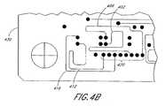
- FIG. 4Billustrates a portion of the MID 1 layer of a printed circuit board in an embodiment of a memory module.
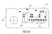
- FIG. 4Cillustrates a portion of the MID 2 layer of a printed circuit board in an embodiment of a memory module.
- FIG. 1Aillustrates the primary side of an embodiment of a memory module 100 .
- the module 100comprises two rows of memory integrated circuits 102 mounted onto a printed circuit board 104 .
- the memory module 100meets the timing standards for and is compatible with JEDEC requirements for a PC133 SDRAM module, but departs from the design guidelines contained in the PC133 design specification. In particular, the memory module 100 meets the timing and interface requirements of the PC133 standard notwithstanding the module 100 having a height (H) of approximately two inches.
- This heightexceeds the 1.75′′ height guideline recommended in the PC133 Design Specification, but allows a single layer of conventional TSOP integrated circuits 102 to be placed in two rows on each side of the printed circuit board 104 , thus avoiding the negative characteristics caused by stacking of integrated circuits and also avoiding the use of more expensive micro-BGA integrated circuits.
- the printed circuit boardmaintains a width (W) of 5.25′′ as defined in the PC133 Design Specification.
- the memory module 100is compatible with the timing requirements while using a greater printed circuit board height through the unique layout and arrangement of the integrated circuits 102 on the printed circuit board and the arrangement of integrated circuit interconnections.
- the upper row of integrated circuits 102(designated U 1 through U 10 ) are oriented in the opposite direction from the lower row of integrated circuits 102 (designated U 11 through U 18 ).
- FIG. 1Billustrates the second side of the embodiment of a memory module 100 .
- the upper row of integrated circuits 102 (designated U 24 through U 33 ) on the second side of the printed circuit board 104are placed in an orientation opposite that of the lower row of integrated circuits 102 (designated U 34 through U 41 ).
- the orientation of each integrated circuit 102can be advantageously determined from an orientation indicia 106 .
- the orientation indiciais a small circular mark 106 on the surface of the integrated circuit 102 .
- the different orientations of the upper row of integrated circuits 102 and the lower row of integrated circuits 102allow the traces on the signal layer of the memory module 100 to be placed such that the trace lengths to the data pins on the integrated circuits 102 in the first (upper) row have substantially the same length as the signal traces to the data pins on the integrated circuits 102 in the second (lower) row.
- FIG. 4Aillustrates a portion of a primary signal layer 400 of the printed circuit board 104 of the embodiment of a memory module 100 illustrated in FIGS. 1A and 1B .
- FIG. 4Billustrates a portion of a MID 1 signal layer 430 of the printed circuit board 104 of the embodiment of a memory module illustrated in FIGS. 1A and 1B .
- FIG. 4 Cillustrates a portion of a MID 2 signal layer 460 of the embodiment of a memory module illustrated in FIGS. 1A and 1B .
- the illustrated portion of the primary signal layer 400connects to the integrated circuits 102 designated U 1 and U 11 .
- a signal trace 404 to one of the data pins of the U 1 integrated circuitis designed to have substantially the same length from the data pin of the U 1 integrated circuit to the primary memory module connector 420 as the length of a signal trace 414 from the corresponding data pin in the U 11 integrated circuit to the primary memory module connector 420 .
- the signal trace 404 from the U 1 integrated circuit to the primary memory module connector 420 and the signal trace 414 from the U 11 integrated circuit to the primary memory module connector 420each include a respective portion of signal trace located on the MID 2 layer 460 of the printed circuit board 104 , as illustrated in FIG. 4 C.
- a signal trace 408 from a second data pin on the U 1 integrated circuit to the primary memory module connector 420is designed to be of substantially the same length as the length of a signal trace 418 from the corresponding pin on the U 11 integrated circuit to the primary memory module connector 420 .
- the signal traces 408 , 418also include respective portions of the traces located on the MID 2 layer 460 of the printed circuit board 104 .
- a signal trace 402 and a signal trace 406 from third and fourth data pins on the U 1 integrated circuit to the primary memory module connector 420are designed to be substantially the same lengths as the lengths of a signal trace 412 and a signal trace 416 from the corresponding data pins on the U 11 integrated circuit to the primary memory module connector 420 .
- the signal traces 402 , 406 , 412 , 416include a portion of the signal trace located on the MID 1 layer 430 of the printed circuit board 104 .
- four signal traces 404 , 408 , 416 , 418include respective resistors 107 affixed to a first set of connection points 407 ( FIG. 4A ) on the primary signal layer 400 of the printed circuit board 104 .
- the four signal traces 402 , 406 , 418 , 414include respective resistors 109 ( FIG. 4A ) affixed to a second set of connection points 409 on the primary signal layer 400 of the printed circuit board 104 .
- the resistors 107 , 109complete the circuit paths from the integrated circuit pins to the connector 420 and also provide impedance matching required in the JEDEC standards.
- the substantially equal signal trace lengthsare repeated for each pair of integrated circuit locations in the first and the second row.
- the portions of the signal traces on the primary signal layer 400 serving an integrated circuit in the first rowhave substantially the same lengths as the signal traces serving a corresponding integrated circuit in the second row.
- the overall lengths of the tracesare configured to be substantially equal (to within 10% of the total trace length) by varying the lengths of the portions of the traces located on the MID 1 layer 430 and the MID 2 layer 460 .
- the data mask trace lengths and the clock trace lengthsadvantageously are maintained to be substantially equal.
- the substantial equality of trace lengthsis achieved without requiring the addition of repetitious back-and-forth (i.e., serpentine) trace portions to the signal traces of the physically closer integrated circuits 102 to equalize the trace lengths of the signal lines of the closer integrated circuits 102 with the trace lengths of the signal lines of the integrated circuits 102 that are located physically farther from a common signal trace connector area 420 .
- serpentinerepetitious back-and-forth
- the timing requirements for the memory module 100are advantageously met through the use of a second level of symmetry in addition to the use of substantially equal trace lengths.
- the address signals to the integrated circuits 102 in the top and bottom roware routed from a common register 302 via a set 303 of signal paths.
- the address signals to the integrated circuits 102 on the second half of the memory module 100are routed from a common register 304 via a second set 305 of signal paths.
- the use of the bilateral symmetryallows closer matching of timing performance for the signals from the integrated circuits 102 , improves the timing performance, and provides greater performance timing margins than traditional design guidelines in which each integrated circuit in a row of integrated circuits 102 is connected to a single register.
- the operation of the memory module 100is synchronized with an external clock signal (not shown) from a computer (not shown) by a clock generator circuit 309 , which is discussed in more detail below in connection with FIG. 3 B.
- FIG. 3Billustrates a half 310 of the block diagram shown in FIG. 3 A.
- the bilateral symmetryutilizes non-contiguous ranges of data bits for each addressing register. Rather than handling the bits in contiguous ranges such as bits 0 - 31 addressed in a first register and bits 32 - 63 addressed in a second register, as described in the JEDEC design guidelines, the first register 302 addresses data bits 0 - 15 (designated D 0 through D 15 ) and data bits 32 - 47 (designated D 32 through D 47 ).
- the second register 304addresses the integrated circuits 102 on the second half of the board (not shown in FIG. 3 B), which store data bits 16 - 31 and bits 48 - 63 .
- Each data bit (designated D 0 through D 63 ) and each check bit (designated CB 0 through CB 7 )connects to the memory module connection interface 314 via a respective signal trace 311 which contains a respective resistive element 312 .
- the resistive elements 312 in FIG. 3Bcorrespond to the resistors 107 , 109 in FIG. 1 A.
- the physical layout of the signal traces 311is illustrated in FIGS. 4A through 4C .
- the use of non-contiguous portions of the data wordadvantageously allows the use of a symmetric layout of the memory module 100 that complies with memory module timing requirements on a physically larger board than envisioned in the design guidelines.
- the use of bilateral symmetry in the board layout and the use of non-contiguous bit rangesis advantageously usable for larger data word lengths than the 64-bit word length given in this embodiment.
- the operation of the memory integrated circuits U 1 -U 18 , U 24 -U 41 and the operation of the common registers 302 , 304are controlled by a plurality of clock signals PCK 0 -PCK 9 from the clock generator circuit 309 .
- the clock generator circuit 309includes a phase locked loop (PLL) (not shown) that operates in a conventional manner to synchronize the clock signals with an input clock signal (CKIN) from the computer (not shown) or other system into which the memory module is inserted.
- PLLphase locked loop
- Each of the clock signals PCK 0 -PCK 8is connected to four memory integrated circuits, and the clock signal PCK 9 is connected to the common registers 302 , 304 .
- the clock signalsare connected to the memory integrated circuits and the common registers as follows (only the connections to the circuits shown in FIG. 3B are illustrated):
- PCK0 U11, U12, U34, U35(D0-D3, D4-D7) PCK1 U13, U14, U36, U37 (D8-D11, D12-D15) PCK2 U15, U16, U38, U39 (D16-D19, D20-D23) PCK3 U17, U18, U40, U41 (D24-D27, D28-D31) PCK4 U1, U2, U24, U25 (D32-D35, D40-D43) PCK5 U3, U4, U26, U27 (D36-D39, D44-D47) PCK6 U1, U2, U24, U25 (D48-D51, D52-D55) PCK7 U9, U10, U32, U33 (D56-D59, D60-D63) PCK8 U5, U6, U28, U29 (CB0-CB3, CB4-CB7) PCK9 control registers 302, 304
- the integrated circuits 102are advantageously mounted on both sides of the printed circuit board 104 .
- the mounting of integrated circuits 102 on both sides of the printed circuit board, and the use of bilateral symmetry of the signal traces on the printed circuit boardadvantageously permits the use of a larger printed circuit board and standard memory integrated circuits 102 .
- the integrated circuits 102 usedare advantageously commercially available 64 Meg by 4-bit (67,108,864 address locations with 4 bits per location) memory integrated circuits for a 1-Gigabyte capacity memory module 100 and are advantageously commercially available 128 Meg by 4-bit (134,217,728 addressed locations with 4 bits per location) memory integrated circuits for a 2-Gigabyte capacity memory module 100 .
- the four data pins of the integrated circuits 102 on the second side of the printed circuit board 104are directly opposite the four data pins of the integrated circuits 102 on the first side of the printed circuit board.
- the data pins of the integrated circuit on the opposite sideare serviced by the signal traces shown in FIG. 4A using a via between the two sides for each signal trace.
- FIG. 2 A and FIG. 2 BAn embodiment of a memory module 200 that is compatible with the timing requirements for Double Data Rate (DDR) SDRAM is shown in FIG. 2 A and FIG. 2 B.
- the DDR SDRAM module 200comprises memory integrated circuits 202 utilizing standard TSOP packaging that are compatible with the JEDEC DDR timing requirements.
- the DDR SDRAM module 200advantageously utilizes bilateral symmetry to achieve the timing requirements specified in the DDR SDRAM requirements on a board 204 having a height (H) of approximately 2 inches and a width (W) of 5.25 inches.
- the integrated circuits 202are oriented, as advantageously indicated by an orientation indicia 106 , in opposite orientations in a first and a second row, respectively.
- the trace lengths of signal traces to the integrated circuits 202 in the first (upper) roware maintained to be substantially the same as the signal traces to integrated circuits 202 in the second (lower) row.
- the integrated circuits 202 mounted to a first half of the memory module 200are routed to a first register 210 and the integrated circuits 202 mounted to a second half of the memory module 200 are routed to a second register 220 .
- each data registerstores non-contiguous portions of the data word.
Landscapes
- Engineering & Computer Science (AREA)
- Microelectronics & Electronic Packaging (AREA)
- Semiconductor Memories (AREA)
- Dram (AREA)
- Static Random-Access Memory (AREA)
Abstract
Description
| PCK0 | U11, U12, U34, U35 | (D0-D3, D4-D7) | ||
| PCK1 | U13, U14, U36, U37 | (D8-D11, D12-D15) | ||
| PCK2 | U15, U16, U38, U39 | (D16-D19, D20-D23) | ||
| PCK3 | U17, U18, U40, U41 | (D24-D27, D28-D31) | ||
| PCK4 | U1, U2, U24, U25 | (D32-D35, D40-D43) | ||
| PCK5 | U3, U4, U26, U27 | (D36-D39, D44-D47) | ||
| PCK6 | U1, U2, U24, U25 | (D48-D51, D52-D55) | ||
| PCK7 | U9, U10, U32, U33 | (D56-D59, D60-D63) | ||
| PCK8 | U5, U6, U28, U29 | (CB0-CB3, CB4-CB7) | ||
| PCK9 | control registers 302, 304 | |||
Claims (15)
Priority Applications (1)
| Application Number | Priority Date | Filing Date | Title |
|---|---|---|---|
| US10/768,534US6873534B2 (en) | 2002-03-07 | 2004-01-30 | Arrangement of integrated circuits in a memory module |
Applications Claiming Priority (2)
| Application Number | Priority Date | Filing Date | Title |
|---|---|---|---|
| US10/094,512US6751113B2 (en) | 2002-03-07 | 2002-03-07 | Arrangement of integrated circuits in a memory module |
| US10/768,534US6873534B2 (en) | 2002-03-07 | 2004-01-30 | Arrangement of integrated circuits in a memory module |
Related Parent Applications (1)
| Application Number | Title | Priority Date | Filing Date |
|---|---|---|---|
| US10/094,512ContinuationUS6751113B2 (en) | 2002-03-07 | 2002-03-07 | Arrangement of integrated circuits in a memory module |
Publications (2)
| Publication Number | Publication Date |
|---|---|
| US20040184301A1 US20040184301A1 (en) | 2004-09-23 |
| US6873534B2true US6873534B2 (en) | 2005-03-29 |
Family
ID=27788121
Family Applications (6)
| Application Number | Title | Priority Date | Filing Date |
|---|---|---|---|
| US10/094,512Expired - LifetimeUS6751113B2 (en) | 2002-03-07 | 2002-03-07 | Arrangement of integrated circuits in a memory module |
| US10/674,082AbandonedUS20040136229A1 (en) | 2002-03-07 | 2003-09-26 | Arrangement of integrated circuits in a memory module |
| US10/674,240AbandonedUS20040057269A1 (en) | 2002-03-07 | 2003-09-29 | Arrangement of integrated circuits in a memory module |
| US10/765,420Expired - LifetimeUS6930900B2 (en) | 2002-03-07 | 2004-01-27 | Arrangement of integrated circuits in a memory module |
| US10/765,488Expired - LifetimeUS6930903B2 (en) | 2002-03-07 | 2004-01-27 | Arrangement of integrated circuits in a memory module |
| US10/768,534Expired - LifetimeUS6873534B2 (en) | 2002-03-07 | 2004-01-30 | Arrangement of integrated circuits in a memory module |
Family Applications Before (5)
| Application Number | Title | Priority Date | Filing Date |
|---|---|---|---|
| US10/094,512Expired - LifetimeUS6751113B2 (en) | 2002-03-07 | 2002-03-07 | Arrangement of integrated circuits in a memory module |
| US10/674,082AbandonedUS20040136229A1 (en) | 2002-03-07 | 2003-09-26 | Arrangement of integrated circuits in a memory module |
| US10/674,240AbandonedUS20040057269A1 (en) | 2002-03-07 | 2003-09-29 | Arrangement of integrated circuits in a memory module |
| US10/765,420Expired - LifetimeUS6930900B2 (en) | 2002-03-07 | 2004-01-27 | Arrangement of integrated circuits in a memory module |
| US10/765,488Expired - LifetimeUS6930903B2 (en) | 2002-03-07 | 2004-01-27 | Arrangement of integrated circuits in a memory module |
Country Status (3)
| Country | Link |
|---|---|
| US (6) | US6751113B2 (en) |
| AU (1) | AU2003213767A1 (en) |
| WO (1) | WO2003077132A1 (en) |
Cited By (78)
| Publication number | Priority date | Publication date | Assignee | Title |
|---|---|---|---|---|
| US20040235222A1 (en)* | 2001-10-26 | 2004-11-25 | Staktek Group, L.P. | Integrated circuit stacking system and method |
| US20060053345A1 (en)* | 2004-09-03 | 2006-03-09 | Staktek Group L.P. | Thin module system and method |
| US20060050488A1 (en)* | 2004-09-03 | 2006-03-09 | Staktel Group, L.P. | High capacity thin module system and method |
| US20060049513A1 (en)* | 2004-09-03 | 2006-03-09 | Staktek Group L.P. | Thin module system and method with thermal management |
| US20060050497A1 (en)* | 2004-09-03 | 2006-03-09 | Staktek Group L.P. | Buffered thin module system and method |
| US20060049500A1 (en)* | 2004-09-03 | 2006-03-09 | Staktek Group L.P. | Thin module system and method |
| US20060050592A1 (en)* | 2004-09-03 | 2006-03-09 | Staktek Group L.P. | Compact module system and method |
| US20060049502A1 (en)* | 2004-09-03 | 2006-03-09 | Staktek Group, L.P. | Module thermal management system and method |
| US20060050496A1 (en)* | 2004-09-03 | 2006-03-09 | Staktek Group L.P. | Thin module system and method |
| US7033861B1 (en) | 2005-05-18 | 2006-04-25 | Staktek Group L.P. | Stacked module systems and method |
| US20060092614A1 (en)* | 2001-10-26 | 2006-05-04 | Staktek Group, L.P. | Stacked module systems and methods |
| US20060125071A1 (en)* | 2004-12-10 | 2006-06-15 | Samsung Electronics Co., Ltd. | Memory module and method of mounting memory device on PCB for memory module |
| US20060136658A1 (en)* | 2004-12-16 | 2006-06-22 | Simpletech, Inc. | DDR2 SDRAM memory module |
| US20060198238A1 (en)* | 2004-09-03 | 2006-09-07 | Staktek Group L.P. | Modified core for circuit module system and method |
| US20060203442A1 (en)* | 2004-09-03 | 2006-09-14 | Staktek Group, L.P. | Memory module system and method |
| US20060261449A1 (en)* | 2005-05-18 | 2006-11-23 | Staktek Group L.P. | Memory module system and method |
| US20070014168A1 (en)* | 2005-06-24 | 2007-01-18 | Rajan Suresh N | Method and circuit for configuring memory core integrated circuit dies with memory interface integrated circuit dies |
| US20070058410A1 (en)* | 2005-09-02 | 2007-03-15 | Rajan Suresh N | Methods and apparatus of stacking DRAMs |
| US7193310B2 (en) | 2001-12-14 | 2007-03-20 | Stuktek Group L.P. | Stacking system and method |
| US7202555B2 (en) | 2001-10-26 | 2007-04-10 | Staktek Group L.P. | Pitch change and chip scale stacking system and method |
| US20070091704A1 (en)* | 2005-10-26 | 2007-04-26 | Siva Raghuram | Memory module with an electronic printed circuit board and a plurality of semiconductor chips of the same type |
| US20070096302A1 (en)* | 2005-10-31 | 2007-05-03 | Josef Schuster | Semiconductor memory module |
| US20070176286A1 (en)* | 2006-02-02 | 2007-08-02 | Staktek Group L.P. | Composite core circuit module system and method |
| US20070201208A1 (en)* | 2006-02-27 | 2007-08-30 | Staktek Group L.P. | Active cooling methods and apparatus for modules |
| US20080025125A1 (en)* | 2006-07-31 | 2008-01-31 | Metaram, Inc. | Interface circuit system and method for performing power management operations in conjunction with only a portion of a memory circuit |
| US20080025108A1 (en)* | 2006-07-31 | 2008-01-31 | Metaram, Inc. | System and method for delaying a signal communicated from a system to at least one of a plurality of memory circuits |
| US20080025137A1 (en)* | 2005-06-24 | 2008-01-31 | Metaram, Inc. | System and method for simulating an aspect of a memory circuit |
| US20080025124A1 (en)* | 2006-07-31 | 2008-01-31 | Metaram, Inc. | Interface circuit system and method for performing power management operations utilizing power management signals |
| US20080025123A1 (en)* | 2006-07-31 | 2008-01-31 | Metaram, Inc. | Interface circuit system and method for autonomously performing power management operations in conjunction with a plurality of memory circuits |
| US20080028135A1 (en)* | 2006-07-31 | 2008-01-31 | Metaram, Inc. | Multiple-component memory interface system and method |
| US20080031072A1 (en)* | 2006-07-31 | 2008-02-07 | Metaram, Inc. | Power saving system and method for use with a plurality of memory circuits |
| US20080082763A1 (en)* | 2006-10-02 | 2008-04-03 | Metaram, Inc. | Apparatus and method for power management of memory circuits by a system or component thereof |
| KR100834826B1 (en) | 2007-01-25 | 2008-06-03 | 삼성전자주식회사 | Integrated circuit module structure with reduced handling damage and terminal resistor arrangement method |
| US7423885B2 (en) | 2004-09-03 | 2008-09-09 | Entorian Technologies, Lp | Die module system |
| US7443023B2 (en) | 2004-09-03 | 2008-10-28 | Entorian Technologies, Lp | High capacity thin module system |
| US7446410B2 (en) | 2004-09-03 | 2008-11-04 | Entorian Technologies, Lp | Circuit module with thermal casing systems |
| US7522421B2 (en) | 2004-09-03 | 2009-04-21 | Entorian Technologies, Lp | Split core circuit module |
| US7542297B2 (en) | 2004-09-03 | 2009-06-02 | Entorian Technologies, Lp | Optimized mounting area circuit module system and method |
| US7579687B2 (en) | 2004-09-03 | 2009-08-25 | Entorian Technologies, Lp | Circuit module turbulence enhancement systems and methods |
| US7581127B2 (en) | 2006-07-31 | 2009-08-25 | Metaram, Inc. | Interface circuit system and method for performing power saving operations during a command-related latency |
| US7616452B2 (en) | 2004-09-03 | 2009-11-10 | Entorian Technologies, Lp | Flex circuit constructions for high capacity circuit module systems and methods |
| US8041881B2 (en) | 2006-07-31 | 2011-10-18 | Google Inc. | Memory device with emulated characteristics |
| US8055833B2 (en) | 2006-10-05 | 2011-11-08 | Google Inc. | System and method for increasing capacity, performance, and flexibility of flash storage |
| US8060774B2 (en) | 2005-06-24 | 2011-11-15 | Google Inc. | Memory systems and memory modules |
| US8077535B2 (en) | 2006-07-31 | 2011-12-13 | Google Inc. | Memory refresh apparatus and method |
| US8081474B1 (en) | 2007-12-18 | 2011-12-20 | Google Inc. | Embossed heat spreader |
| US8080874B1 (en) | 2007-09-14 | 2011-12-20 | Google Inc. | Providing additional space between an integrated circuit and a circuit board for positioning a component therebetween |
| US8090897B2 (en) | 2006-07-31 | 2012-01-03 | Google Inc. | System and method for simulating an aspect of a memory circuit |
| US8089795B2 (en) | 2006-02-09 | 2012-01-03 | Google Inc. | Memory module with memory stack and interface with enhanced capabilities |
| US8111566B1 (en) | 2007-11-16 | 2012-02-07 | Google, Inc. | Optimal channel design for memory devices for providing a high-speed memory interface |
| US8130560B1 (en) | 2006-11-13 | 2012-03-06 | Google Inc. | Multi-rank partial width memory modules |
| US8169233B2 (en) | 2009-06-09 | 2012-05-01 | Google Inc. | Programming of DIMM termination resistance values |
| US8209479B2 (en) | 2007-07-18 | 2012-06-26 | Google Inc. | Memory circuit system and method |
| US8244971B2 (en) | 2006-07-31 | 2012-08-14 | Google Inc. | Memory circuit system and method |
| US8280714B2 (en) | 2006-07-31 | 2012-10-02 | Google Inc. | Memory circuit simulation system and method with refresh capabilities |
| US8327104B2 (en) | 2006-07-31 | 2012-12-04 | Google Inc. | Adjusting the timing of signals associated with a memory system |
| US8335894B1 (en) | 2008-07-25 | 2012-12-18 | Google Inc. | Configurable memory system with interface circuit |
| US8386722B1 (en) | 2008-06-23 | 2013-02-26 | Google Inc. | Stacked DIMM memory interface |
| US8397013B1 (en) | 2006-10-05 | 2013-03-12 | Google Inc. | Hybrid memory module |
| US8438328B2 (en) | 2008-02-21 | 2013-05-07 | Google Inc. | Emulation of abstracted DIMMs using abstracted DRAMs |
| US8566516B2 (en) | 2006-07-31 | 2013-10-22 | Google Inc. | Refresh management of memory modules |
| US8588017B2 (en) | 2010-10-20 | 2013-11-19 | Samsung Electronics Co., Ltd. | Memory circuits, systems, and modules for performing DRAM refresh operations and methods of operating the same |
| US8796830B1 (en) | 2006-09-01 | 2014-08-05 | Google Inc. | Stackable low-profile lead frame package |
| US8930647B1 (en) | 2011-04-06 | 2015-01-06 | P4tents1, LLC | Multiple class memory systems |
| US9158546B1 (en) | 2011-04-06 | 2015-10-13 | P4tents1, LLC | Computer program product for fetching from a first physical memory between an execution of a plurality of threads associated with a second physical memory |
| US9164679B2 (en) | 2011-04-06 | 2015-10-20 | Patents1, Llc | System, method and computer program product for multi-thread operation involving first memory of a first memory class and second memory of a second memory class |
| US9170744B1 (en) | 2011-04-06 | 2015-10-27 | P4tents1, LLC | Computer program product for controlling a flash/DRAM/embedded DRAM-equipped system |
| US9171585B2 (en) | 2005-06-24 | 2015-10-27 | Google Inc. | Configurable memory circuit system and method |
| US9176671B1 (en) | 2011-04-06 | 2015-11-03 | P4tents1, LLC | Fetching data between thread execution in a flash/DRAM/embedded DRAM-equipped system |
| US9250954B2 (en) | 2013-01-17 | 2016-02-02 | Xockets, Inc. | Offload processor modules for connection to system memory, and corresponding methods and systems |
| US9258276B2 (en) | 2012-05-22 | 2016-02-09 | Xockets, Inc. | Efficient packet handling, redirection, and inspection using offload processors |
| US9286472B2 (en) | 2012-05-22 | 2016-03-15 | Xockets, Inc. | Efficient packet handling, redirection, and inspection using offload processors |
| US9378161B1 (en) | 2013-01-17 | 2016-06-28 | Xockets, Inc. | Full bandwidth packet handling with server systems including offload processors |
| US9417754B2 (en) | 2011-08-05 | 2016-08-16 | P4tents1, LLC | User interface system, method, and computer program product |
| US9507739B2 (en) | 2005-06-24 | 2016-11-29 | Google Inc. | Configurable memory circuit system and method |
| US9542352B2 (en) | 2006-02-09 | 2017-01-10 | Google Inc. | System and method for reducing command scheduling constraints of memory circuits |
| US9632929B2 (en) | 2006-02-09 | 2017-04-25 | Google Inc. | Translating an address associated with a command communicated between a system and memory circuits |
| US10013371B2 (en) | 2005-06-24 | 2018-07-03 | Google Llc | Configurable memory circuit system and method |
Families Citing this family (47)
| Publication number | Priority date | Publication date | Assignee | Title |
|---|---|---|---|---|
| US8058142B2 (en) | 1996-11-04 | 2011-11-15 | Besang Inc. | Bonded semiconductor structure and method of making the same |
| US20050280155A1 (en)* | 2004-06-21 | 2005-12-22 | Sang-Yun Lee | Semiconductor bonding and layer transfer method |
| US6751113B2 (en) | 2002-03-07 | 2004-06-15 | Netlist, Inc. | Arrangement of integrated circuits in a memory module |
| US7200024B2 (en) | 2002-08-02 | 2007-04-03 | Micron Technology, Inc. | System and method for optically interconnecting memory devices |
| US7117316B2 (en)* | 2002-08-05 | 2006-10-03 | Micron Technology, Inc. | Memory hub and access method having internal row caching |
| US7254331B2 (en)* | 2002-08-09 | 2007-08-07 | Micron Technology, Inc. | System and method for multiple bit optical data transmission in memory systems |
| US7149874B2 (en) | 2002-08-16 | 2006-12-12 | Micron Technology, Inc. | Memory hub bypass circuit and method |
| US7836252B2 (en) | 2002-08-29 | 2010-11-16 | Micron Technology, Inc. | System and method for optimizing interconnections of memory devices in a multichip module |
| US7102907B2 (en) | 2002-09-09 | 2006-09-05 | Micron Technology, Inc. | Wavelength division multiplexed memory module, memory system and method |
| US20100133695A1 (en)* | 2003-01-12 | 2010-06-03 | Sang-Yun Lee | Electronic circuit with embedded memory |
| US7799675B2 (en)* | 2003-06-24 | 2010-09-21 | Sang-Yun Lee | Bonded semiconductor structure and method of fabricating the same |
| US7245145B2 (en) | 2003-06-11 | 2007-07-17 | Micron Technology, Inc. | Memory module and method having improved signal routing topology |
| US7120727B2 (en) | 2003-06-19 | 2006-10-10 | Micron Technology, Inc. | Reconfigurable memory module and method |
| US7260685B2 (en)* | 2003-06-20 | 2007-08-21 | Micron Technology, Inc. | Memory hub and access method having internal prefetch buffers |
| US7428644B2 (en) | 2003-06-20 | 2008-09-23 | Micron Technology, Inc. | System and method for selective memory module power management |
| US7863748B2 (en)* | 2003-06-24 | 2011-01-04 | Oh Choonsik | Semiconductor circuit and method of fabricating the same |
| US8071438B2 (en)* | 2003-06-24 | 2011-12-06 | Besang Inc. | Semiconductor circuit |
| US20100190334A1 (en)* | 2003-06-24 | 2010-07-29 | Sang-Yun Lee | Three-dimensional semiconductor structure and method of manufacturing the same |
| US7867822B2 (en) | 2003-06-24 | 2011-01-11 | Sang-Yun Lee | Semiconductor memory device |
| US7120743B2 (en) | 2003-10-20 | 2006-10-10 | Micron Technology, Inc. | Arbitration system and method for memory responses in a hub-based memory system |
| US7023719B1 (en)* | 2003-10-23 | 2006-04-04 | Lsi Logic Corporation | Memory module having mirrored placement of DRAM integrated circuits upon a four-layer printed circuit board |
| US7234070B2 (en) | 2003-10-27 | 2007-06-19 | Micron Technology, Inc. | System and method for using a learning sequence to establish communications on a high-speed nonsynchronous interface in the absence of clock forwarding |
| KR100574951B1 (en)* | 2003-10-31 | 2006-05-02 | 삼성전자주식회사 | Memory module with improved register placement structure |
| US20050018495A1 (en)* | 2004-01-29 | 2005-01-27 | Netlist, Inc. | Arrangement of integrated circuits in a memory module |
| US7181584B2 (en) | 2004-02-05 | 2007-02-20 | Micron Technology, Inc. | Dynamic command and/or address mirroring system and method for memory modules |
| US7366864B2 (en) | 2004-03-08 | 2008-04-29 | Micron Technology, Inc. | Memory hub architecture having programmable lane widths |
| US7120723B2 (en) | 2004-03-25 | 2006-10-10 | Micron Technology, Inc. | System and method for memory hub-based expansion bus |
| US7590797B2 (en) | 2004-04-08 | 2009-09-15 | Micron Technology, Inc. | System and method for optimizing interconnections of components in a multichip memory module |
| DE102004021226A1 (en)* | 2004-04-30 | 2005-11-24 | Infineon Technologies Ag | Semiconductor circuit module, e.g. for memory chips, has chips in two groups aligned at 180 degrees to each other so that each branch of signal line ends lies in y-direction |
| US7222213B2 (en)* | 2004-05-17 | 2007-05-22 | Micron Technology, Inc. | System and method for communicating the synchronization status of memory modules during initialization of the memory modules |
| US7392331B2 (en) | 2004-08-31 | 2008-06-24 | Micron Technology, Inc. | System and method for transmitting data packets in a computer system having a memory hub architecture |
| JP4754235B2 (en)* | 2005-02-21 | 2011-08-24 | Ntn株式会社 | Rotation transmission device |
| US7212424B2 (en)* | 2005-03-21 | 2007-05-01 | Hewlett-Packard Development Company, L.P. | Double-high DIMM with dual registers and related methods |
| US8455978B2 (en) | 2010-05-27 | 2013-06-04 | Sang-Yun Lee | Semiconductor circuit structure and method of making the same |
| US8367524B2 (en)* | 2005-03-29 | 2013-02-05 | Sang-Yun Lee | Three-dimensional integrated circuit structure |
| US20110143506A1 (en)* | 2009-12-10 | 2011-06-16 | Sang-Yun Lee | Method for fabricating a semiconductor memory device |
| US7457978B2 (en)* | 2005-05-09 | 2008-11-25 | Micron Technology, Inc. | Adjustable byte lane offset for memory module to reduce skew |
| US7414312B2 (en)* | 2005-05-24 | 2008-08-19 | Kingston Technology Corp. | Memory-module board layout for use with memory chips of different data widths |
| KR100715287B1 (en)* | 2006-04-26 | 2007-05-08 | 삼성전자주식회사 | Semiconductor memory module |
| US7663939B2 (en)* | 2006-05-30 | 2010-02-16 | Kingston Technology Corporation | Voltage stabilizer memory module |
| US8040710B2 (en)* | 2007-05-31 | 2011-10-18 | Qimonda Ag | Semiconductor memory arrangement |
| US7839712B2 (en)* | 2007-08-03 | 2010-11-23 | Qimonda Ag | Semiconductor memory arrangement |
| JP4372189B2 (en)* | 2007-12-27 | 2009-11-25 | 株式会社東芝 | Information processing apparatus and nonvolatile semiconductor memory drive |
| US20100195277A1 (en)* | 2009-02-05 | 2010-08-05 | Trident Microsystems, Inc. | Dual Layer Printed Circuit Board |
| US8723335B2 (en) | 2010-05-20 | 2014-05-13 | Sang-Yun Lee | Semiconductor circuit structure and method of forming the same using a capping layer |
| US8289727B2 (en)* | 2010-06-11 | 2012-10-16 | Taiwan Semiconductor Manufacturing Company, Ltd. | Package substrate |
| US8437164B1 (en)* | 2011-07-27 | 2013-05-07 | Apple Inc. | Stacked memory device for a configurable bandwidth memory interface |
Citations (55)
| Publication number | Priority date | Publication date | Assignee | Title |
|---|---|---|---|---|
| US4280176A (en) | 1978-12-26 | 1981-07-21 | International Business Machines Corporation | Memory configuration, address interleaving, relocation and access control system |
| JPS6034054A (en) | 1983-08-04 | 1985-02-21 | Nec Corp | Module of memory integrated circuit |
| US4679167A (en) | 1983-07-29 | 1987-07-07 | Hewlett-Packard Company | Apparatus for locating a memory module within a memory space |
| US5012389A (en) | 1988-12-14 | 1991-04-30 | Hand Held Products, Inc. | Board wiring pattern for a high density memory module |
| US5164916A (en) | 1992-03-31 | 1992-11-17 | Digital Equipment Corporation | High-density double-sided multi-string memory module with resistor for insertion detection |
| US5191404A (en) | 1989-12-20 | 1993-03-02 | Digital Equipment Corporation | High density memory array packaging |
| US5226136A (en) | 1986-05-06 | 1993-07-06 | Nintendo Company Limited | Memory cartridge bank selecting apparatus |
| US5303123A (en) | 1992-12-21 | 1994-04-12 | Alcatel Network Systems, Inc. | Retainer for removable circuit board components |
| US5383148A (en) | 1992-05-19 | 1995-01-17 | Sun Microsystems, Inc. | Single in-line memory module |
| US5412538A (en) | 1993-07-19 | 1995-05-02 | Cordata, Inc. | Space-saving memory module |
| US5428762A (en) | 1992-03-11 | 1995-06-27 | International Business Machines Corporation | Expandable memory having plural memory cards for distributively storing system data |
| US5495435A (en) | 1993-11-18 | 1996-02-27 | Nec Corporation | Synchronous DRAM memory module |
| US5513135A (en) | 1994-12-02 | 1996-04-30 | International Business Machines Corporation | Synchronous memory packaged in single/dual in-line memory module and method of fabrication |
| US5541448A (en) | 1991-10-16 | 1996-07-30 | Texas Instruments Inc. | Electronic circuit card |
| US5572691A (en) | 1993-04-21 | 1996-11-05 | Gi Corporation | Apparatus and method for providing multiple data streams from stored data using dual memory buffers |
| US5606717A (en)* | 1990-04-18 | 1997-02-25 | Rambus, Inc. | Memory circuitry having bus interface for receiving information in packets and access time registers |
| US5631807A (en) | 1995-01-20 | 1997-05-20 | Minnesota Mining And Manufacturing Company | Electronic circuit structure with aperture suspended component |
| US5642323A (en) | 1993-06-17 | 1997-06-24 | Matsushita Electric Industrial Co., Ltd. | Semiconductor integrated circuit with a data transmission circuit |
| US5652861A (en) | 1993-02-24 | 1997-07-29 | Digital Equipment Corporation | System for interleaving memory modules and banks |
| US5652462A (en) | 1993-04-05 | 1997-07-29 | Matsushita Electric Industrial Co., Ltd. | Multilevel semiconductor integrated circuit device |
| US5661339A (en) | 1992-09-16 | 1997-08-26 | Clayton; James E. | Thin multichip module |
| US5691946A (en) | 1996-12-03 | 1997-11-25 | International Business Machines Corporation | Row redundancy block architecture |
| US5712811A (en) | 1995-05-17 | 1998-01-27 | Lg Semicon Co., Ltd. | IC memory card |
| US5737192A (en) | 1993-04-30 | 1998-04-07 | The United States Of America As Represented By The Secretary Of The Air Force | Density improvement in integration modules |
| US5754408A (en) | 1995-11-29 | 1998-05-19 | Mitsubishi Semiconductor America, Inc. | Stackable double-density integrated circuit assemblies |
| US5835932A (en) | 1997-03-13 | 1998-11-10 | Silicon Aquarius, Inc. | Methods and systems for maintaining data locality in a multiple memory bank system having DRAM with integral SRAM |
| US5847985A (en) | 1997-03-24 | 1998-12-08 | Mitsubishi Denki Kabushiki Kaisha | Memory modules |
| US5867448A (en) | 1997-06-11 | 1999-02-02 | Cypress Semiconductor Corp. | Buffer for memory modules with trace delay compensation |
| US5953738A (en) | 1997-07-02 | 1999-09-14 | Silicon Aquarius, Inc | DRAM with integral SRAM and arithmetic-logic units |
| US6021048A (en) | 1998-02-17 | 2000-02-01 | Smith; Gary W. | High speed memory module |
| US6072744A (en) | 1998-07-21 | 2000-06-06 | Hyundai Electronics Industries Co., Ltd. | Memory device having data bus lines of uniform length |
| US6097619A (en) | 1998-06-19 | 2000-08-01 | Compaq Computer Corp. | Symmetric memory board |
| US6151235A (en) | 1998-09-22 | 2000-11-21 | Nucore Technology Inc. | Card type semiconductor memory device for storing analog image signals in separate analog memory card units |
| US6157538A (en) | 1998-12-07 | 2000-12-05 | Intel Corporation | Heat dissipation apparatus and method |
| US6181004B1 (en) | 1999-01-22 | 2001-01-30 | Jerry D. Koontz | Digital signal processing assembly and test method |
| US6215718B1 (en) | 1998-06-11 | 2001-04-10 | Texas Instruments Incorporated | Architecture for large capacity high-speed random access memory |
| US6222737B1 (en) | 1999-04-23 | 2001-04-24 | Dense-Pac Microsystems, Inc. | Universal package and method of forming the same |
| US6222739B1 (en) | 1998-01-20 | 2001-04-24 | Viking Components | High-density computer module with stacked parallel-plane packaging |
| US6353539B1 (en) | 1998-07-21 | 2002-03-05 | Intel Corporation | Method and apparatus for matched length routing of back-to-back package placement |
| US20020088633A1 (en) | 2001-01-08 | 2002-07-11 | Kong Eun Youp | Multi-chip memory devices, modules and control methods including independent control of memory chips |
| US6502161B1 (en) | 2000-01-05 | 2002-12-31 | Rambus Inc. | Memory system including a point-to-point linked memory subsystem |
| US20030014578A1 (en) | 2001-07-11 | 2003-01-16 | Pax George E. | Routability for memeory devices |
| US6532158B1 (en) | 1999-08-25 | 2003-03-11 | Smartdata Sa | Electronic apparatus comprising a group of chipcards |
| US20030051091A1 (en) | 1991-11-05 | 2003-03-13 | Leung Wing Yu | Latched sense amplifiers as high speed memory in a memory system |
| US20030048616A1 (en) | 2001-09-10 | 2003-03-13 | Samsung Electronics Co., Ltd. | Memory module |
| US20030057564A1 (en) | 1997-04-04 | 2003-03-27 | Elm Technology Corporation | Three dimensional structure memory |
| US6545895B1 (en) | 2002-04-22 | 2003-04-08 | High Connection Density, Inc. | High capacity SDRAM memory module with stacked printed circuit boards |
| US20030075789A1 (en) | 1999-08-06 | 2003-04-24 | Masayasu Kawamura | Semiconductor storage device having memory chips in a stacked structure |
| US20030090879A1 (en) | 2001-06-14 | 2003-05-15 | Doblar Drew G. | Dual inline memory module |
| US6594167B1 (en) | 1999-09-16 | 2003-07-15 | Mitsubishi Denki Kabushiki Kaisha | Semiconductor integrated circuit having a structure for equalizing interconnection lengths and memory module provided with the semiconductor integrated circuit |
| US6617695B1 (en)* | 2000-05-30 | 2003-09-09 | Mitsubishi Denki Kabushiki Kaisha | Semiconductor device and semiconductor module using the same |
| US6705877B1 (en) | 2003-01-17 | 2004-03-16 | High Connection Density, Inc. | Stackable memory module with variable bandwidth |
| US6751113B2 (en)* | 2002-03-07 | 2004-06-15 | Netlist, Inc. | Arrangement of integrated circuits in a memory module |
| US6757751B1 (en) | 2000-08-11 | 2004-06-29 | Harrison Gene | High-speed, multiple-bank, stacked, and PCB-mounted memory module |
| US6766433B2 (en) | 2001-09-21 | 2004-07-20 | Freescale Semiconductor, Inc. | System having user programmable addressing modes and method therefor |
Family Cites Families (25)
| Publication number | Priority date | Publication date | Assignee | Title |
|---|---|---|---|---|
| US5452231A (en)* | 1988-10-05 | 1995-09-19 | Quickturn Design Systems, Inc. | Hierarchically connected reconfigurable logic assembly |
| US5465435A (en)* | 1995-02-21 | 1995-11-14 | Malvaez; Laura A. | Shower step for shaving legs |
| IN188196B (en)* | 1995-05-15 | 2002-08-31 | Silicon Graphics Inc | |
| US5743408A (en)* | 1996-05-16 | 1998-04-28 | Hill; Mark Langdon | Leather automobile trim |
| US5994997A (en)* | 1997-11-24 | 1999-11-30 | Motorola, Inc. | Thick-film resistor having concentric terminals and method therefor |
| JP3718039B2 (en)* | 1997-12-17 | 2005-11-16 | 株式会社日立製作所 | Semiconductor device and electronic device using the same |
| US5912507A (en)* | 1998-02-04 | 1999-06-15 | Motorola, Inc. | Solderable pad with integral series termination resistor |
| US6225035B1 (en)* | 1998-03-18 | 2001-05-01 | Motorola, Inc. | Method for forming a thick-film resistor |
| US6446184B2 (en) | 1998-04-28 | 2002-09-03 | International Business Machines Corporation | Address re-mapping for memory module using presence detect data |
| US6171921B1 (en)* | 1998-06-05 | 2001-01-09 | Motorola, Inc. | Method for forming a thick-film resistor and thick-film resistor formed thereby |
| US6108212A (en)* | 1998-06-05 | 2000-08-22 | Motorola, Inc. | Surface-mount device package having an integral passive component |
| US6232042B1 (en)* | 1998-07-07 | 2001-05-15 | Motorola, Inc. | Method for manufacturing an integral thin-film metal resistor |
| US6185654B1 (en)* | 1998-07-17 | 2001-02-06 | Compaq Computer Corporation | Phantom resource memory address mapping system |
| JP2000148656A (en)* | 1998-11-09 | 2000-05-30 | Mitsubishi Electric Corp | Memory system |
| US6349456B1 (en) | 1998-12-31 | 2002-02-26 | Motorola, Inc. | Method of manufacturing photodefined integral capacitor with self-aligned dielectric and electrodes |
| US6103134A (en)* | 1998-12-31 | 2000-08-15 | Motorola, Inc. | Circuit board features with reduced parasitic capacitance and method therefor |
| US6194990B1 (en)* | 1999-03-16 | 2001-02-27 | Motorola, Inc. | Printed circuit board with a multilayer integral thin-film metal resistor and method therefor |
| US6256866B1 (en) | 1999-05-11 | 2001-07-10 | Motorola, Inc. | Polymer thick-film resistor printed on planar circuit board surface |
| US6364649B1 (en)* | 1999-10-07 | 2002-04-02 | Fibrex Insulations, Inc. | Apparatus for making pipe insulation |
| US6353867B1 (en)* | 2000-01-14 | 2002-03-05 | Insilicon Corporation | Virtual component on-chip interface |
| GB0006432D0 (en)* | 2000-03-17 | 2000-05-03 | Stanelco Fibre Optics Ltd | Capsules |
| JP4480855B2 (en)* | 2000-06-08 | 2010-06-16 | 富士通マイクロエレクトロニクス株式会社 | Module including semiconductor device and system including module |
| US6342164B1 (en) | 2000-07-31 | 2002-01-29 | Motorola, Inc. | Pinhole-free dielectric films |
| US6625685B1 (en)* | 2000-09-20 | 2003-09-23 | Broadcom Corporation | Memory controller with programmable configuration |
| US6594712B1 (en)* | 2000-10-20 | 2003-07-15 | Banderacom, Inc. | Inifiniband channel adapter for performing direct DMA between PCI bus and inifiniband link |
- 2002
- 2002-03-07USUS10/094,512patent/US6751113B2/ennot_activeExpired - Lifetime
- 2003
- 2003-03-06WOPCT/US2003/006978patent/WO2003077132A1/ennot_activeApplication Discontinuation
- 2003-03-06AUAU2003213767Apatent/AU2003213767A1/ennot_activeAbandoned
- 2003-09-26USUS10/674,082patent/US20040136229A1/ennot_activeAbandoned
- 2003-09-29USUS10/674,240patent/US20040057269A1/ennot_activeAbandoned
- 2004
- 2004-01-27USUS10/765,420patent/US6930900B2/ennot_activeExpired - Lifetime
- 2004-01-27USUS10/765,488patent/US6930903B2/ennot_activeExpired - Lifetime
- 2004-01-30USUS10/768,534patent/US6873534B2/ennot_activeExpired - Lifetime
Patent Citations (59)
| Publication number | Priority date | Publication date | Assignee | Title |
|---|---|---|---|---|
| US4280176A (en) | 1978-12-26 | 1981-07-21 | International Business Machines Corporation | Memory configuration, address interleaving, relocation and access control system |
| US4679167A (en) | 1983-07-29 | 1987-07-07 | Hewlett-Packard Company | Apparatus for locating a memory module within a memory space |
| JPS6034054A (en) | 1983-08-04 | 1985-02-21 | Nec Corp | Module of memory integrated circuit |
| US5226136A (en) | 1986-05-06 | 1993-07-06 | Nintendo Company Limited | Memory cartridge bank selecting apparatus |
| US5012389A (en) | 1988-12-14 | 1991-04-30 | Hand Held Products, Inc. | Board wiring pattern for a high density memory module |
| US5191404A (en) | 1989-12-20 | 1993-03-02 | Digital Equipment Corporation | High density memory array packaging |
| US5606717A (en)* | 1990-04-18 | 1997-02-25 | Rambus, Inc. | Memory circuitry having bus interface for receiving information in packets and access time registers |
| US5541448A (en) | 1991-10-16 | 1996-07-30 | Texas Instruments Inc. | Electronic circuit card |
| US20030051091A1 (en) | 1991-11-05 | 2003-03-13 | Leung Wing Yu | Latched sense amplifiers as high speed memory in a memory system |
| US5428762A (en) | 1992-03-11 | 1995-06-27 | International Business Machines Corporation | Expandable memory having plural memory cards for distributively storing system data |
| US5164916A (en) | 1992-03-31 | 1992-11-17 | Digital Equipment Corporation | High-density double-sided multi-string memory module with resistor for insertion detection |
| US5465229A (en) | 1992-05-19 | 1995-11-07 | Sun Microsystems, Inc. | Single in-line memory module |
| US5383148A (en) | 1992-05-19 | 1995-01-17 | Sun Microsystems, Inc. | Single in-line memory module |
| US5532954A (en) | 1992-05-19 | 1996-07-02 | Sun Microsystems, Inc. | Single in-line memory module |
| US5973951A (en) | 1992-05-19 | 1999-10-26 | Sun Microsystems, Inc. | Single in-line memory module |
| US5661339A (en) | 1992-09-16 | 1997-08-26 | Clayton; James E. | Thin multichip module |
| US5303123A (en) | 1992-12-21 | 1994-04-12 | Alcatel Network Systems, Inc. | Retainer for removable circuit board components |
| US5652861A (en) | 1993-02-24 | 1997-07-29 | Digital Equipment Corporation | System for interleaving memory modules and banks |
| US5652462A (en) | 1993-04-05 | 1997-07-29 | Matsushita Electric Industrial Co., Ltd. | Multilevel semiconductor integrated circuit device |
| US5572691A (en) | 1993-04-21 | 1996-11-05 | Gi Corporation | Apparatus and method for providing multiple data streams from stored data using dual memory buffers |
| US5737192A (en) | 1993-04-30 | 1998-04-07 | The United States Of America As Represented By The Secretary Of The Air Force | Density improvement in integration modules |
| US5642323A (en) | 1993-06-17 | 1997-06-24 | Matsushita Electric Industrial Co., Ltd. | Semiconductor integrated circuit with a data transmission circuit |
| US5412538A (en) | 1993-07-19 | 1995-05-02 | Cordata, Inc. | Space-saving memory module |
| US5495435A (en) | 1993-11-18 | 1996-02-27 | Nec Corporation | Synchronous DRAM memory module |
| US5513135A (en) | 1994-12-02 | 1996-04-30 | International Business Machines Corporation | Synchronous memory packaged in single/dual in-line memory module and method of fabrication |
| US5631807A (en) | 1995-01-20 | 1997-05-20 | Minnesota Mining And Manufacturing Company | Electronic circuit structure with aperture suspended component |
| US5712811A (en) | 1995-05-17 | 1998-01-27 | Lg Semicon Co., Ltd. | IC memory card |
| US5754408A (en) | 1995-11-29 | 1998-05-19 | Mitsubishi Semiconductor America, Inc. | Stackable double-density integrated circuit assemblies |
| US5691946A (en) | 1996-12-03 | 1997-11-25 | International Business Machines Corporation | Row redundancy block architecture |
| US5835932A (en) | 1997-03-13 | 1998-11-10 | Silicon Aquarius, Inc. | Methods and systems for maintaining data locality in a multiple memory bank system having DRAM with integral SRAM |
| US5847985A (en) | 1997-03-24 | 1998-12-08 | Mitsubishi Denki Kabushiki Kaisha | Memory modules |
| US20030057564A1 (en) | 1997-04-04 | 2003-03-27 | Elm Technology Corporation | Three dimensional structure memory |
| US5867448A (en) | 1997-06-11 | 1999-02-02 | Cypress Semiconductor Corp. | Buffer for memory modules with trace delay compensation |
| US5953738A (en) | 1997-07-02 | 1999-09-14 | Silicon Aquarius, Inc | DRAM with integral SRAM and arithmetic-logic units |
| US6222739B1 (en) | 1998-01-20 | 2001-04-24 | Viking Components | High-density computer module with stacked parallel-plane packaging |
| US6021048A (en) | 1998-02-17 | 2000-02-01 | Smith; Gary W. | High speed memory module |
| US6215718B1 (en) | 1998-06-11 | 2001-04-10 | Texas Instruments Incorporated | Architecture for large capacity high-speed random access memory |
| US6097619A (en) | 1998-06-19 | 2000-08-01 | Compaq Computer Corp. | Symmetric memory board |
| US6353539B1 (en) | 1998-07-21 | 2002-03-05 | Intel Corporation | Method and apparatus for matched length routing of back-to-back package placement |
| US6072744A (en) | 1998-07-21 | 2000-06-06 | Hyundai Electronics Industries Co., Ltd. | Memory device having data bus lines of uniform length |
| US6151235A (en) | 1998-09-22 | 2000-11-21 | Nucore Technology Inc. | Card type semiconductor memory device for storing analog image signals in separate analog memory card units |
| US6157538A (en) | 1998-12-07 | 2000-12-05 | Intel Corporation | Heat dissipation apparatus and method |
| US6181004B1 (en) | 1999-01-22 | 2001-01-30 | Jerry D. Koontz | Digital signal processing assembly and test method |
| US6222737B1 (en) | 1999-04-23 | 2001-04-24 | Dense-Pac Microsystems, Inc. | Universal package and method of forming the same |
| US20030075789A1 (en) | 1999-08-06 | 2003-04-24 | Masayasu Kawamura | Semiconductor storage device having memory chips in a stacked structure |
| US6532158B1 (en) | 1999-08-25 | 2003-03-11 | Smartdata Sa | Electronic apparatus comprising a group of chipcards |
| US6594167B1 (en) | 1999-09-16 | 2003-07-15 | Mitsubishi Denki Kabushiki Kaisha | Semiconductor integrated circuit having a structure for equalizing interconnection lengths and memory module provided with the semiconductor integrated circuit |
| US6502161B1 (en) | 2000-01-05 | 2002-12-31 | Rambus Inc. | Memory system including a point-to-point linked memory subsystem |
| US20030061447A1 (en) | 2000-01-05 | 2003-03-27 | Perego Richard E. | Memory system including a point-to-point linked memory subsystem |
| US6617695B1 (en)* | 2000-05-30 | 2003-09-09 | Mitsubishi Denki Kabushiki Kaisha | Semiconductor device and semiconductor module using the same |
| US6757751B1 (en) | 2000-08-11 | 2004-06-29 | Harrison Gene | High-speed, multiple-bank, stacked, and PCB-mounted memory module |
| US20020088633A1 (en) | 2001-01-08 | 2002-07-11 | Kong Eun Youp | Multi-chip memory devices, modules and control methods including independent control of memory chips |
| US20030090879A1 (en) | 2001-06-14 | 2003-05-15 | Doblar Drew G. | Dual inline memory module |
| US20030014578A1 (en) | 2001-07-11 | 2003-01-16 | Pax George E. | Routability for memeory devices |
| US20030048616A1 (en) | 2001-09-10 | 2003-03-13 | Samsung Electronics Co., Ltd. | Memory module |
| US6766433B2 (en) | 2001-09-21 | 2004-07-20 | Freescale Semiconductor, Inc. | System having user programmable addressing modes and method therefor |
| US6751113B2 (en)* | 2002-03-07 | 2004-06-15 | Netlist, Inc. | Arrangement of integrated circuits in a memory module |
| US6545895B1 (en) | 2002-04-22 | 2003-04-08 | High Connection Density, Inc. | High capacity SDRAM memory module with stacked printed circuit boards |
| US6705877B1 (en) | 2003-01-17 | 2004-03-16 | High Connection Density, Inc. | Stackable memory module with variable bandwidth |
Non-Patent Citations (8)
| Title |
|---|
| Intel Corporation, 66/100 MHz PC SDRAM 64-Bit Non-ECC/Parity 144 Pin Unbuffered SO-DIMM Specification, Revision 1.0, Feb. 1999. |
| Intel, PC SDRAM Registered DIMM Design Support Document, Revision 1.2, Oct. 1998. |
| JEDEC Standard No. 21-C, 4.20.2-168 Pin, PC133 SDRAM Registered DIMM Design Specification, Revision 1.4, Release 11a, Feb. 2002. |
| JEDEC Standard No. 21-C, 4.20.3-144 Pin, PC133 SDRAM Unbuffered SO-DIMM, Reference Design Specification, Revision 1.02, Release 11. |
| JEDEC Standard No. 21-C, 4.20.5-184 Pin PC1600/2100 DDR SDRAM Unbuffered DIMM Design Specification, Revision 1.1, Release 11b. |
| JEDEC Standard No. 21-C, 4.20.6-200 Pin, PC2700/PC2100/PC1600 DDR SDRAM Unbuffered SO-DIMM Reference Design Specification, Revision 1.1, Release 11b, Apr. 26, 2002. |
| JEDEC Standard No. 21-C, DDR SDRAM PC2100 and PC1600 DDR SDRAM Registered DIMM Design Specification, Revision 1.3, Release 11b, Jan. 2002. |
| PCT International Search Report dated Aug. 29, 2003 for counterpart PCT application No. PCT US/03/06978 filed Mar. 6, 2003, in 5 pages. |
Cited By (213)
| Publication number | Priority date | Publication date | Assignee | Title |
|---|---|---|---|---|
| US20060092614A1 (en)* | 2001-10-26 | 2006-05-04 | Staktek Group, L.P. | Stacked module systems and methods |
| US7656678B2 (en) | 2001-10-26 | 2010-02-02 | Entorian Technologies, Lp | Stacked module systems |
| US20040235222A1 (en)* | 2001-10-26 | 2004-11-25 | Staktek Group, L.P. | Integrated circuit stacking system and method |
| US7595550B2 (en) | 2001-10-26 | 2009-09-29 | Entorian Technologies, Lp | Flex-based circuit module |
| US7202555B2 (en) | 2001-10-26 | 2007-04-10 | Staktek Group L.P. | Pitch change and chip scale stacking system and method |
| US7193310B2 (en) | 2001-12-14 | 2007-03-20 | Stuktek Group L.P. | Stacking system and method |
| US7606050B2 (en) | 2004-09-03 | 2009-10-20 | Entorian Technologies, Lp | Compact module system and method |
| US7423885B2 (en) | 2004-09-03 | 2008-09-09 | Entorian Technologies, Lp | Die module system |
| US20060050496A1 (en)* | 2004-09-03 | 2006-03-09 | Staktek Group L.P. | Thin module system and method |
| US20060050492A1 (en)* | 2004-09-03 | 2006-03-09 | Staktek Group, L.P. | Thin module system and method |
| US20080278901A9 (en)* | 2004-09-03 | 2008-11-13 | Staktek Group, L.P. | Memory module system and method |
| US20060050592A1 (en)* | 2004-09-03 | 2006-03-09 | Staktek Group L.P. | Compact module system and method |
| US20080278924A1 (en)* | 2004-09-03 | 2008-11-13 | Entorian Technologies, L.P. (Formerly Staktek Group L.P.) | Die module system |
| US7446410B2 (en) | 2004-09-03 | 2008-11-04 | Entorian Technologies, Lp | Circuit module with thermal casing systems |
| US20060198238A1 (en)* | 2004-09-03 | 2006-09-07 | Staktek Group L.P. | Modified core for circuit module system and method |
| US20060203442A1 (en)* | 2004-09-03 | 2006-09-14 | Staktek Group, L.P. | Memory module system and method |
| US7443023B2 (en) | 2004-09-03 | 2008-10-28 | Entorian Technologies, Lp | High capacity thin module system |
| US7606040B2 (en) | 2004-09-03 | 2009-10-20 | Entorian Technologies, Lp | Memory module system and method |
| US7616452B2 (en) | 2004-09-03 | 2009-11-10 | Entorian Technologies, Lp | Flex circuit constructions for high capacity circuit module systems and methods |
| US7606049B2 (en) | 2004-09-03 | 2009-10-20 | Entorian Technologies, Lp | Module thermal management system and method |
| US20060049500A1 (en)* | 2004-09-03 | 2006-03-09 | Staktek Group L.P. | Thin module system and method |
| US20060050497A1 (en)* | 2004-09-03 | 2006-03-09 | Staktek Group L.P. | Buffered thin module system and method |
| US7468893B2 (en) | 2004-09-03 | 2008-12-23 | Entorian Technologies, Lp | Thin module system and method |
| US7606042B2 (en)* | 2004-09-03 | 2009-10-20 | Entorian Technologies, Lp | High capacity thin module system and method |
| US20070111606A1 (en)* | 2004-09-03 | 2007-05-17 | Staktek Group L.P., A Texas Limited Partnership | Buffered Thin Module System and Method |
| US20060049502A1 (en)* | 2004-09-03 | 2006-03-09 | Staktek Group, L.P. | Module thermal management system and method |
| US7768796B2 (en) | 2004-09-03 | 2010-08-03 | Entorian Technologies L.P. | Die module system |
| US7602613B2 (en) | 2004-09-03 | 2009-10-13 | Entorian Technologies, Lp | Thin module system and method |
| US20060049513A1 (en)* | 2004-09-03 | 2006-03-09 | Staktek Group L.P. | Thin module system and method with thermal management |
| US20060050488A1 (en)* | 2004-09-03 | 2006-03-09 | Staktel Group, L.P. | High capacity thin module system and method |
| US7626259B2 (en) | 2004-09-03 | 2009-12-01 | Entorian Technologies, Lp | Heat sink for a high capacity thin module system |
| US7324352B2 (en) | 2004-09-03 | 2008-01-29 | Staktek Group L.P. | High capacity thin module system and method |
| US20060053345A1 (en)* | 2004-09-03 | 2006-03-09 | Staktek Group L.P. | Thin module system and method |
| US7737549B2 (en) | 2004-09-03 | 2010-06-15 | Entorian Technologies Lp | Circuit module with thermal casing systems |
| US7579687B2 (en) | 2004-09-03 | 2009-08-25 | Entorian Technologies, Lp | Circuit module turbulence enhancement systems and methods |
| US7542297B2 (en) | 2004-09-03 | 2009-06-02 | Entorian Technologies, Lp | Optimized mounting area circuit module system and method |
| US7522421B2 (en) | 2004-09-03 | 2009-04-21 | Entorian Technologies, Lp | Split core circuit module |
| US7522425B2 (en)* | 2004-09-03 | 2009-04-21 | Entorian Technologies, Lp | High capacity thin module system and method |
| US20080030966A1 (en)* | 2004-09-03 | 2008-02-07 | Staktek Group L.P. | High Capacity Thin Module System and Method |
| US20080030972A1 (en)* | 2004-09-03 | 2008-02-07 | Staktek Group L.P. | High Capacity Thin Module System and Method |
| US7511968B2 (en) | 2004-09-03 | 2009-03-31 | Entorian Technologies, Lp | Buffered thin module system and method |
| US7459784B2 (en) | 2004-09-03 | 2008-12-02 | Entorian Technologies, Lp | High capacity thin module system |
| US20090052124A1 (en)* | 2004-09-03 | 2009-02-26 | Entorian Technologies, L.P. (Formerly Staktek Group, L.P) | Circuit Module with Thermal Casing Systems |
| US7480152B2 (en) | 2004-09-03 | 2009-01-20 | Entorian Technologies, Lp | Thin module system and method |
| US7760513B2 (en) | 2004-09-03 | 2010-07-20 | Entorian Technologies Lp | Modified core for circuit module system and method |
| US20060125071A1 (en)* | 2004-12-10 | 2006-06-15 | Samsung Electronics Co., Ltd. | Memory module and method of mounting memory device on PCB for memory module |
| US7348219B2 (en)* | 2004-12-10 | 2008-03-25 | Samsung Electronics Co., Ltd. | Method of mounting memory device on PCB for memory module |
| US20060136658A1 (en)* | 2004-12-16 | 2006-06-22 | Simpletech, Inc. | DDR2 SDRAM memory module |
| US20070126124A1 (en)* | 2005-05-18 | 2007-06-07 | Staktek Group L.P. | Memory Module System and Method |
| US20070126125A1 (en)* | 2005-05-18 | 2007-06-07 | Staktek Group L.P. | Memory Module System and Method |
| US20060261449A1 (en)* | 2005-05-18 | 2006-11-23 | Staktek Group L.P. | Memory module system and method |
| US7033861B1 (en) | 2005-05-18 | 2006-04-25 | Staktek Group L.P. | Stacked module systems and method |
| US20070050530A1 (en)* | 2005-06-24 | 2007-03-01 | Rajan Suresh N | Integrated memory core and memory interface circuit |
| US20080025137A1 (en)* | 2005-06-24 | 2008-01-31 | Metaram, Inc. | System and method for simulating an aspect of a memory circuit |
| US8359187B2 (en) | 2005-06-24 | 2013-01-22 | Google Inc. | Simulating a different number of memory circuit devices |
| US7609567B2 (en) | 2005-06-24 | 2009-10-27 | Metaram, Inc. | System and method for simulating an aspect of a memory circuit |
| US20070014168A1 (en)* | 2005-06-24 | 2007-01-18 | Rajan Suresh N | Method and circuit for configuring memory core integrated circuit dies with memory interface integrated circuit dies |
| US8386833B2 (en) | 2005-06-24 | 2013-02-26 | Google Inc. | Memory systems and memory modules |
| US8060774B2 (en) | 2005-06-24 | 2011-11-15 | Google Inc. | Memory systems and memory modules |
| US10013371B2 (en) | 2005-06-24 | 2018-07-03 | Google Llc | Configurable memory circuit system and method |
| US7515453B2 (en) | 2005-06-24 | 2009-04-07 | Metaram, Inc. | Integrated memory core and memory interface circuit |
| US8615679B2 (en) | 2005-06-24 | 2013-12-24 | Google Inc. | Memory modules with reliability and serviceability functions |
| US9507739B2 (en) | 2005-06-24 | 2016-11-29 | Google Inc. | Configurable memory circuit system and method |
| US9171585B2 (en) | 2005-06-24 | 2015-10-27 | Google Inc. | Configurable memory circuit system and method |
| US8582339B2 (en) | 2005-09-02 | 2013-11-12 | Google Inc. | System including memory stacks |
| US8811065B2 (en) | 2005-09-02 | 2014-08-19 | Google Inc. | Performing error detection on DRAMs |
| US8619452B2 (en) | 2005-09-02 | 2013-12-31 | Google Inc. | Methods and apparatus of stacking DRAMs |
| US20070058410A1 (en)* | 2005-09-02 | 2007-03-15 | Rajan Suresh N | Methods and apparatus of stacking DRAMs |
| US7379316B2 (en) | 2005-09-02 | 2008-05-27 | Metaram, Inc. | Methods and apparatus of stacking DRAMs |
| US20070091704A1 (en)* | 2005-10-26 | 2007-04-26 | Siva Raghuram | Memory module with an electronic printed circuit board and a plurality of semiconductor chips of the same type |
| US7375971B2 (en)* | 2005-10-26 | 2008-05-20 | Infineon Technologies Ag | Memory module with an electronic printed circuit board and a plurality of semiconductor chips of the same type |
| US7315454B2 (en)* | 2005-10-31 | 2008-01-01 | Infineon Technologies Ag | Semiconductor memory module |
| US20070096302A1 (en)* | 2005-10-31 | 2007-05-03 | Josef Schuster | Semiconductor memory module |
| US7511969B2 (en) | 2006-02-02 | 2009-03-31 | Entorian Technologies, Lp | Composite core circuit module system and method |
| US20070176286A1 (en)* | 2006-02-02 | 2007-08-02 | Staktek Group L.P. | Composite core circuit module system and method |
| US9727458B2 (en) | 2006-02-09 | 2017-08-08 | Google Inc. | Translating an address associated with a command communicated between a system and memory circuits |
| US8089795B2 (en) | 2006-02-09 | 2012-01-03 | Google Inc. | Memory module with memory stack and interface with enhanced capabilities |
| US9542352B2 (en) | 2006-02-09 | 2017-01-10 | Google Inc. | System and method for reducing command scheduling constraints of memory circuits |
| US9542353B2 (en) | 2006-02-09 | 2017-01-10 | Google Inc. | System and method for reducing command scheduling constraints of memory circuits |
| US9632929B2 (en) | 2006-02-09 | 2017-04-25 | Google Inc. | Translating an address associated with a command communicated between a system and memory circuits |
| US8797779B2 (en) | 2006-02-09 | 2014-08-05 | Google Inc. | Memory module with memory stack and interface with enhanced capabilites |
| US8566556B2 (en) | 2006-02-09 | 2013-10-22 | Google Inc. | Memory module with memory stack and interface with enhanced capabilities |
| US7289327B2 (en) | 2006-02-27 | 2007-10-30 | Stakick Group L.P. | Active cooling methods and apparatus for modules |
| US20070201208A1 (en)* | 2006-02-27 | 2007-08-30 | Staktek Group L.P. | Active cooling methods and apparatus for modules |
| US8972673B2 (en) | 2006-07-31 | 2015-03-03 | Google Inc. | Power management of memory circuits by virtual memory simulation |
| US8340953B2 (en) | 2006-07-31 | 2012-12-25 | Google, Inc. | Memory circuit simulation with power saving capabilities |
| US7581127B2 (en) | 2006-07-31 | 2009-08-25 | Metaram, Inc. | Interface circuit system and method for performing power saving operations during a command-related latency |
| US7724589B2 (en) | 2006-07-31 | 2010-05-25 | Google Inc. | System and method for delaying a signal communicated from a system to at least one of a plurality of memory circuits |
| US8090897B2 (en) | 2006-07-31 | 2012-01-03 | Google Inc. | System and method for simulating an aspect of a memory circuit |
| US7386656B2 (en) | 2006-07-31 | 2008-06-10 | Metaram, Inc. | Interface circuit system and method for performing power management operations in conjunction with only a portion of a memory circuit |
| US7580312B2 (en) | 2006-07-31 | 2009-08-25 | Metaram, Inc. | Power saving system and method for use with a plurality of memory circuits |
| US7472220B2 (en) | 2006-07-31 | 2008-12-30 | Metaram, Inc. | Interface circuit system and method for performing power management operations utilizing power management signals |
| US8154935B2 (en) | 2006-07-31 | 2012-04-10 | Google Inc. | Delaying a signal communicated from a system to at least one of a plurality of memory circuits |
| US7392338B2 (en) | 2006-07-31 | 2008-06-24 | Metaram, Inc. | Interface circuit system and method for autonomously performing power management operations in conjunction with a plurality of memory circuits |
| US7590796B2 (en) | 2006-07-31 | 2009-09-15 | Metaram, Inc. | System and method for power management in memory systems |
| US8244971B2 (en) | 2006-07-31 | 2012-08-14 | Google Inc. | Memory circuit system and method |
| US8280714B2 (en) | 2006-07-31 | 2012-10-02 | Google Inc. | Memory circuit simulation system and method with refresh capabilities |
| US8327104B2 (en) | 2006-07-31 | 2012-12-04 | Google Inc. | Adjusting the timing of signals associated with a memory system |
| US20080025108A1 (en)* | 2006-07-31 | 2008-01-31 | Metaram, Inc. | System and method for delaying a signal communicated from a system to at least one of a plurality of memory circuits |
| US8631220B2 (en) | 2006-07-31 | 2014-01-14 | Google Inc. | Adjusting the timing of signals associated with a memory system |
| US9047976B2 (en) | 2006-07-31 | 2015-06-02 | Google Inc. | Combined signal delay and power saving for use with a plurality of memory circuits |
| US8077535B2 (en) | 2006-07-31 | 2011-12-13 | Google Inc. | Memory refresh apparatus and method |
| US20080025125A1 (en)* | 2006-07-31 | 2008-01-31 | Metaram, Inc. | Interface circuit system and method for performing power management operations in conjunction with only a portion of a memory circuit |
| US20080025123A1 (en)* | 2006-07-31 | 2008-01-31 | Metaram, Inc. | Interface circuit system and method for autonomously performing power management operations in conjunction with a plurality of memory circuits |
| US8868829B2 (en) | 2006-07-31 | 2014-10-21 | Google Inc. | Memory circuit system and method |
| US20080025124A1 (en)* | 2006-07-31 | 2008-01-31 | Metaram, Inc. | Interface circuit system and method for performing power management operations utilizing power management signals |
| US8041881B2 (en) | 2006-07-31 | 2011-10-18 | Google Inc. | Memory device with emulated characteristics |
| US8566516B2 (en) | 2006-07-31 | 2013-10-22 | Google Inc. | Refresh management of memory modules |
| US20080028135A1 (en)* | 2006-07-31 | 2008-01-31 | Metaram, Inc. | Multiple-component memory interface system and method |
| US20080031072A1 (en)* | 2006-07-31 | 2008-02-07 | Metaram, Inc. | Power saving system and method for use with a plurality of memory circuits |
| US8745321B2 (en) | 2006-07-31 | 2014-06-03 | Google Inc. | Simulating a memory standard |
| US8796830B1 (en) | 2006-09-01 | 2014-08-05 | Google Inc. | Stackable low-profile lead frame package |
| US20080082763A1 (en)* | 2006-10-02 | 2008-04-03 | Metaram, Inc. | Apparatus and method for power management of memory circuits by a system or component thereof |
| US8977806B1 (en) | 2006-10-05 | 2015-03-10 | Google Inc. | Hybrid memory module |
| US8370566B2 (en) | 2006-10-05 | 2013-02-05 | Google Inc. | System and method for increasing capacity, performance, and flexibility of flash storage |
| US8397013B1 (en) | 2006-10-05 | 2013-03-12 | Google Inc. | Hybrid memory module |
| US8751732B2 (en) | 2006-10-05 | 2014-06-10 | Google Inc. | System and method for increasing capacity, performance, and flexibility of flash storage |
| US8055833B2 (en) | 2006-10-05 | 2011-11-08 | Google Inc. | System and method for increasing capacity, performance, and flexibility of flash storage |
| US8760936B1 (en) | 2006-11-13 | 2014-06-24 | Google Inc. | Multi-rank partial width memory modules |
| US8130560B1 (en) | 2006-11-13 | 2012-03-06 | Google Inc. | Multi-rank partial width memory modules |
| US8446781B1 (en) | 2006-11-13 | 2013-05-21 | Google Inc. | Multi-rank partial width memory modules |
| KR100834826B1 (en) | 2007-01-25 | 2008-06-03 | 삼성전자주식회사 | Integrated circuit module structure with reduced handling damage and terminal resistor arrangement method |
| US8209479B2 (en) | 2007-07-18 | 2012-06-26 | Google Inc. | Memory circuit system and method |
| US8080874B1 (en) | 2007-09-14 | 2011-12-20 | Google Inc. | Providing additional space between an integrated circuit and a circuit board for positioning a component therebetween |
| US8111566B1 (en) | 2007-11-16 | 2012-02-07 | Google, Inc. | Optimal channel design for memory devices for providing a high-speed memory interface |
| US8675429B1 (en) | 2007-11-16 | 2014-03-18 | Google Inc. | Optimal channel design for memory devices for providing a high-speed memory interface |
| US8081474B1 (en) | 2007-12-18 | 2011-12-20 | Google Inc. | Embossed heat spreader |
| US8730670B1 (en) | 2007-12-18 | 2014-05-20 | Google Inc. | Embossed heat spreader |
| US8705240B1 (en) | 2007-12-18 | 2014-04-22 | Google Inc. | Embossed heat spreader |
| US8438328B2 (en) | 2008-02-21 | 2013-05-07 | Google Inc. | Emulation of abstracted DIMMs using abstracted DRAMs |
| US8631193B2 (en) | 2008-02-21 | 2014-01-14 | Google Inc. | Emulation of abstracted DIMMS using abstracted DRAMS |
| US8386722B1 (en) | 2008-06-23 | 2013-02-26 | Google Inc. | Stacked DIMM memory interface |
| US8762675B2 (en) | 2008-06-23 | 2014-06-24 | Google Inc. | Memory system for synchronous data transmission |
| US8335894B1 (en) | 2008-07-25 | 2012-12-18 | Google Inc. | Configurable memory system with interface circuit |
| US8819356B2 (en) | 2008-07-25 | 2014-08-26 | Google Inc. | Configurable multirank memory system with interface circuit |
| US8169233B2 (en) | 2009-06-09 | 2012-05-01 | Google Inc. | Programming of DIMM termination resistance values |
| US8588017B2 (en) | 2010-10-20 | 2013-11-19 | Samsung Electronics Co., Ltd. | Memory circuits, systems, and modules for performing DRAM refresh operations and methods of operating the same |
| US9176671B1 (en) | 2011-04-06 | 2015-11-03 | P4tents1, LLC | Fetching data between thread execution in a flash/DRAM/embedded DRAM-equipped system |
| US9195395B1 (en) | 2011-04-06 | 2015-11-24 | P4tents1, LLC | Flash/DRAM/embedded DRAM-equipped system and method |
| US9223507B1 (en) | 2011-04-06 | 2015-12-29 | P4tents1, LLC | System, method and computer program product for fetching data between an execution of a plurality of threads |
| US9158546B1 (en) | 2011-04-06 | 2015-10-13 | P4tents1, LLC | Computer program product for fetching from a first physical memory between an execution of a plurality of threads associated with a second physical memory |
| US9189442B1 (en) | 2011-04-06 | 2015-11-17 | P4tents1, LLC | Fetching data between thread execution in a flash/DRAM/embedded DRAM-equipped system |
| US9182914B1 (en) | 2011-04-06 | 2015-11-10 | P4tents1, LLC | System, method and computer program product for multi-thread operation involving first memory of a first memory class and second memory of a second memory class |
| US8930647B1 (en) | 2011-04-06 | 2015-01-06 | P4tents1, LLC | Multiple class memory systems |
| US9164679B2 (en) | 2011-04-06 | 2015-10-20 | Patents1, Llc | System, method and computer program product for multi-thread operation involving first memory of a first memory class and second memory of a second memory class |
| US9170744B1 (en) | 2011-04-06 | 2015-10-27 | P4tents1, LLC | Computer program product for controlling a flash/DRAM/embedded DRAM-equipped system |
| US10338736B1 (en) | 2011-08-05 | 2019-07-02 | P4tents1, LLC | Devices, methods, and graphical user interfaces for manipulating user interface objects with visual and/or haptic feedback |
| US10365758B1 (en) | 2011-08-05 | 2019-07-30 | P4tents1, LLC | Devices, methods, and graphical user interfaces for manipulating user interface objects with visual and/or haptic feedback |
| US11740727B1 (en) | 2011-08-05 | 2023-08-29 | P4Tents1 Llc | Devices, methods, and graphical user interfaces for manipulating user interface objects with visual and/or haptic feedback |
| US11061503B1 (en) | 2011-08-05 | 2021-07-13 | P4tents1, LLC | Devices, methods, and graphical user interfaces for manipulating user interface objects with visual and/or haptic feedback |
| US10996787B1 (en) | 2011-08-05 | 2021-05-04 | P4tents1, LLC | Gesture-equipped touch screen system, method, and computer program product |
| US10936114B1 (en) | 2011-08-05 | 2021-03-02 | P4tents1, LLC | Gesture-equipped touch screen system, method, and computer program product |
| US9417754B2 (en) | 2011-08-05 | 2016-08-16 | P4tents1, LLC | User interface system, method, and computer program product |
| US10838542B1 (en) | 2011-08-05 | 2020-11-17 | P4tents1, LLC | Gesture-equipped touch screen system, method, and computer program product |
| US10788931B1 (en) | 2011-08-05 | 2020-09-29 | P4tents1, LLC | Devices, methods, and graphical user interfaces for manipulating user interface objects with visual and/or haptic feedback |
| US10782819B1 (en) | 2011-08-05 | 2020-09-22 | P4tents1, LLC | Gesture-equipped touch screen system, method, and computer program product |
| US10725581B1 (en) | 2011-08-05 | 2020-07-28 | P4tents1, LLC | Devices, methods and graphical user interfaces for manipulating user interface objects with visual and/or haptic feedback |
| US10671213B1 (en) | 2011-08-05 | 2020-06-02 | P4tents1, LLC | Devices, methods, and graphical user interfaces for manipulating user interface objects with visual and/or haptic feedback |
| US10671212B1 (en) | 2011-08-05 | 2020-06-02 | P4tents1, LLC | Gesture-equipped touch screen system, method, and computer program product |
| US10664097B1 (en) | 2011-08-05 | 2020-05-26 | P4tents1, LLC | Devices, methods, and graphical user interfaces for manipulating user interface objects with visual and/or haptic feedback |
| US10656757B1 (en) | 2011-08-05 | 2020-05-19 | P4tents1, LLC | Gesture-equipped touch screen system, method, and computer program product |
| US10031607B1 (en) | 2011-08-05 | 2018-07-24 | P4tents1, LLC | System, method, and computer program product for a multi-pressure selection touch screen |
| US10120480B1 (en) | 2011-08-05 | 2018-11-06 | P4tents1, LLC | Application-specific pressure-sensitive touch screen system, method, and computer program product |
| US10146353B1 (en) | 2011-08-05 | 2018-12-04 | P4tents1, LLC | Touch screen system, method, and computer program product |
| US10156921B1 (en) | 2011-08-05 | 2018-12-18 | P4tents1, LLC | Tri-state gesture-equipped touch screen system, method, and computer program product |
| US10162448B1 (en) | 2011-08-05 | 2018-12-25 | P4tents1, LLC | System, method, and computer program product for a pressure-sensitive touch screen for messages |
| US10203794B1 (en) | 2011-08-05 | 2019-02-12 | P4tents1, LLC | Pressure-sensitive home interface system, method, and computer program product |
| US10209809B1 (en) | 2011-08-05 | 2019-02-19 | P4tents1, LLC | Pressure-sensitive touch screen system, method, and computer program product for objects |
| US10209806B1 (en) | 2011-08-05 | 2019-02-19 | P4tents1, LLC | Tri-state gesture-equipped touch screen system, method, and computer program product |
| US10209807B1 (en) | 2011-08-05 | 2019-02-19 | P4tents1, LLC | Pressure sensitive touch screen system, method, and computer program product for hyperlinks |
| US10209808B1 (en) | 2011-08-05 | 2019-02-19 | P4tents1, LLC | Pressure-based interface system, method, and computer program product with virtual display layers |
| US10222895B1 (en) | 2011-08-05 | 2019-03-05 | P4tents1, LLC | Pressure-based touch screen system, method, and computer program product with virtual display layers |
| US10222893B1 (en) | 2011-08-05 | 2019-03-05 | P4tents1, LLC | Pressure-based touch screen system, method, and computer program product with virtual display layers |
| US10222894B1 (en) | 2011-08-05 | 2019-03-05 | P4tents1, LLC | System, method, and computer program product for a multi-pressure selection touch screen |
| US10222891B1 (en) | 2011-08-05 | 2019-03-05 | P4tents1, LLC | Setting interface system, method, and computer program product for a multi-pressure selection touch screen |
| US10222892B1 (en) | 2011-08-05 | 2019-03-05 | P4tents1, LLC | System, method, and computer program product for a multi-pressure selection touch screen |
| US10275086B1 (en) | 2011-08-05 | 2019-04-30 | P4tents1, LLC | Gesture-equipped touch screen system, method, and computer program product |
| US10275087B1 (en) | 2011-08-05 | 2019-04-30 | P4tents1, LLC | Devices, methods, and graphical user interfaces for manipulating user interface objects with visual and/or haptic feedback |
| US10656753B1 (en) | 2011-08-05 | 2020-05-19 | P4tents1, LLC | Gesture-equipped touch screen system, method, and computer program product |
| US10345961B1 (en) | 2011-08-05 | 2019-07-09 | P4tents1, LLC | Devices and methods for navigating between user interfaces |
| US10656754B1 (en) | 2011-08-05 | 2020-05-19 | P4tents1, LLC | Devices and methods for navigating between user interfaces |
| US10386960B1 (en) | 2011-08-05 | 2019-08-20 | P4tents1, LLC | Devices, methods, and graphical user interfaces for manipulating user interface objects with visual and/or haptic feedback |
| US10521047B1 (en) | 2011-08-05 | 2019-12-31 | P4tents1, LLC | Gesture-equipped touch screen system, method, and computer program product |
| US10534474B1 (en) | 2011-08-05 | 2020-01-14 | P4tents1, LLC | Gesture-equipped touch screen system, method, and computer program product |
| US10540039B1 (en) | 2011-08-05 | 2020-01-21 | P4tents1, LLC | Devices and methods for navigating between user interface |
| US10551966B1 (en) | 2011-08-05 | 2020-02-04 | P4tents1, LLC | Gesture-equipped touch screen system, method, and computer program product |
| US10592039B1 (en) | 2011-08-05 | 2020-03-17 | P4tents1, LLC | Gesture-equipped touch screen system, method, and computer program product for displaying multiple active applications |
| US10606396B1 (en) | 2011-08-05 | 2020-03-31 | P4tents1, LLC | Gesture-equipped touch screen methods for duration-based functions |
| US10642413B1 (en) | 2011-08-05 | 2020-05-05 | P4tents1, LLC | Gesture-equipped touch screen system, method, and computer program product |
| US10649579B1 (en) | 2011-08-05 | 2020-05-12 | P4tents1, LLC | Devices, methods, and graphical user interfaces for manipulating user interface objects with visual and/or haptic feedback |
| US10649580B1 (en) | 2011-08-05 | 2020-05-12 | P4tents1, LLC | Devices, methods, and graphical use interfaces for manipulating user interface objects with visual and/or haptic feedback |
| US10649578B1 (en) | 2011-08-05 | 2020-05-12 | P4tents1, LLC | Gesture-equipped touch screen system, method, and computer program product |
| US10649571B1 (en) | 2011-08-05 | 2020-05-12 | P4tents1, LLC | Devices, methods, and graphical user interfaces for manipulating user interface objects with visual and/or haptic feedback |
| US10649581B1 (en) | 2011-08-05 | 2020-05-12 | P4tents1, LLC | Devices, methods, and graphical user interfaces for manipulating user interface objects with visual and/or haptic feedback |
| US10656759B1 (en) | 2011-08-05 | 2020-05-19 | P4tents1, LLC | Devices, methods, and graphical user interfaces for manipulating user interface objects with visual and/or haptic feedback |
| US10656756B1 (en) | 2011-08-05 | 2020-05-19 | P4tents1, LLC | Gesture-equipped touch screen system, method, and computer program product |
| US10656752B1 (en) | 2011-08-05 | 2020-05-19 | P4tents1, LLC | Gesture-equipped touch screen system, method, and computer program product |
| US10656758B1 (en) | 2011-08-05 | 2020-05-19 | P4tents1, LLC | Gesture-equipped touch screen system, method, and computer program product |
| US10656755B1 (en) | 2011-08-05 | 2020-05-19 | P4tents1, LLC | Gesture-equipped touch screen system, method, and computer program product |
| US9619406B2 (en) | 2012-05-22 | 2017-04-11 | Xockets, Inc. | Offloading of computation for rack level servers and corresponding methods and systems |
| US9495308B2 (en) | 2012-05-22 | 2016-11-15 | Xockets, Inc. | Offloading of computation for rack level servers and corresponding methods and systems |
| US9258276B2 (en) | 2012-05-22 | 2016-02-09 | Xockets, Inc. | Efficient packet handling, redirection, and inspection using offload processors |
| US9558351B2 (en) | 2012-05-22 | 2017-01-31 | Xockets, Inc. | Processing structured and unstructured data using offload processors |
| US9665503B2 (en) | 2012-05-22 | 2017-05-30 | Xockets, Inc. | Efficient packet handling, redirection, and inspection using offload processors |
| US9286472B2 (en) | 2012-05-22 | 2016-03-15 | Xockets, Inc. | Efficient packet handling, redirection, and inspection using offload processors |
| US9288101B1 (en) | 2013-01-17 | 2016-03-15 | Xockets, Inc. | Full bandwidth packet handling with server systems including offload processors |
| US9436638B1 (en) | 2013-01-17 | 2016-09-06 | Xockets, Inc. | Full bandwidth packet handling with server systems including offload processors |
| US9348638B2 (en) | 2013-01-17 | 2016-05-24 | Xockets, Inc. | Offload processor modules for connection to system memory, and corresponding methods and systems |
| US9378161B1 (en) | 2013-01-17 | 2016-06-28 | Xockets, Inc. | Full bandwidth packet handling with server systems including offload processors |
| US9250954B2 (en) | 2013-01-17 | 2016-02-02 | Xockets, Inc. | Offload processor modules for connection to system memory, and corresponding methods and systems |
| US9460031B1 (en) | 2013-01-17 | 2016-10-04 | Xockets, Inc. | Full bandwidth packet handling with server systems including offload processors |
| US9436639B1 (en) | 2013-01-17 | 2016-09-06 | Xockets, Inc. | Full bandwidth packet handling with server systems including offload processors |
| US9436640B1 (en) | 2013-01-17 | 2016-09-06 | Xockets, Inc. | Full bandwidth packet handling with server systems including offload processors |
Also Published As
| Publication number | Publication date |
|---|---|
| US6751113B2 (en) | 2004-06-15 |
| US20040057269A1 (en) | 2004-03-25 |
| US20040184301A1 (en) | 2004-09-23 |
| US20040184300A1 (en) | 2004-09-23 |
| WO2003077132A1 (en) | 2003-09-18 |
| WO2003077132A8 (en) | 2003-12-18 |
| US20030169614A1 (en) | 2003-09-11 |
| US6930903B2 (en) | 2005-08-16 |
| AU2003213767A1 (en) | 2003-09-22 |
| US6930900B2 (en) | 2005-08-16 |
| US20040136229A1 (en) | 2004-07-15 |
| US20040184299A1 (en) | 2004-09-23 |
Similar Documents
| Publication | Publication Date | Title |
|---|---|---|
| US6873534B2 (en) | Arrangement of integrated circuits in a memory module | |
| US20050018495A1 (en) | Arrangement of integrated circuits in a memory module | |
| US7053478B2 (en) | Pitch change and chip scale stacking system | |
| KR100235222B1 (en) | Single in-line memory module | |
| US6705877B1 (en) | Stackable memory module with variable bandwidth | |
| US7405471B2 (en) | Carrier-based electronic module | |
| US7616452B2 (en) | Flex circuit constructions for high capacity circuit module systems and methods | |
| US6545895B1 (en) | High capacity SDRAM memory module with stacked printed circuit boards | |
| US8864500B1 (en) | Electronic module with flexible portion | |
| US7443023B2 (en) | High capacity thin module system | |
| EP1894201B1 (en) | Memory device identification | |
| US7233501B1 (en) | Interleaved memory heat sink | |
| US6597062B1 (en) | Short channel, memory module with stacked printed circuit boards | |
| US20060050497A1 (en) | Buffered thin module system and method | |
| US7863091B2 (en) | Planar array contact memory cards | |
| US20060048385A1 (en) | Minimized profile circuit module systems and methods | |
| US7309914B2 (en) | Inverted CSP stacking system and method | |
| US20070258278A1 (en) | Memory module and methods for making and using the same | |
| US7606040B2 (en) | Memory module system and method | |
| US20080266778A1 (en) | Memory module routing | |
| US20080030943A1 (en) | Memory module having improved arrangement of discrete devices | |
| EP1475836B1 (en) | Circuit module having interleaved groups of circuit chips | |
| US7202555B2 (en) | Pitch change and chip scale stacking system and method | |
| TWI749838B (en) | Electronic module | |
| JP2000091729A (en) | Stack memory module |
Legal Events
| Date | Code | Title | Description |
|---|---|---|---|
| STCF | Information on status: patent grant | Free format text:PATENTED CASE | |
| FPAY | Fee payment | Year of fee payment:4 | |
| FPAY | Fee payment | Year of fee payment:8 | |
| AS | Assignment | Owner name:DBD CREDIT FUNDING LLC, NEW YORK Free format text:SECURITY AGREEMENT;ASSIGNOR:NETLIST, INC.;REEL/FRAME:030830/0945 Effective date:20130718 | |
| AS | Assignment | Owner name:SVIC NO. 28 NEW TECHNOLOGY BUSINESS INVESTMENT L.L.P., KOREA, REPUBLIC OF Free format text:SECURITY INTEREST;ASSIGNOR:NETLIST, INC.;REEL/FRAME:037150/0897 Effective date:20151118 Owner name:SVIC NO. 28 NEW TECHNOLOGY BUSINESS INVESTMENT L.L Free format text:SECURITY INTEREST;ASSIGNOR:NETLIST, INC.;REEL/FRAME:037150/0897 Effective date:20151118 | |
| AS | Assignment | Owner name:NETLIST, INC., CALIFORNIA Free format text:TERMINATION OF INTELLECTUAL PROPERTY SECURITY AGREEMENT;ASSIGNOR:DBD CREDIT FUNDING LLC;REEL/FRAME:037209/0158 Effective date:20151119 | |
| REMI | Maintenance fee reminder mailed | ||
| FPAY | Fee payment | Year of fee payment:12 | |
| SULP | Surcharge for late payment | Year of fee payment:11 | |
| AS | Assignment | Owner name:NETLIST, INC, CALIFORNIA Free format text:RELEASE BY SECURED PARTY;ASSIGNOR:SVIC. NO. 28 NEW TECHNOLOGY BUSINESS INVESTMENT L.L.P.;REEL/FRAME:065629/0328 Effective date:20231027 |