US6873087B1 - High precision orientation alignment and gap control stages for imprint lithography processes - Google Patents
High precision orientation alignment and gap control stages for imprint lithography processesDownload PDFInfo
- Publication number
- US6873087B1 US6873087B1US09/698,317US69831700AUS6873087B1US 6873087 B1US6873087 B1US 6873087B1US 69831700 AUS69831700 AUS 69831700AUS 6873087 B1US6873087 B1US 6873087B1
- Authority
- US
- United States
- Prior art keywords
- flexure
- spaced
- mount
- axis
- apart
- Prior art date
- Legal status (The legal status is an assumption and is not a legal conclusion. Google has not performed a legal analysis and makes no representation as to the accuracy of the status listed.)
- Expired - Lifetime, expires
Links
Images


Classifications
- G—PHYSICS
- G03—PHOTOGRAPHY; CINEMATOGRAPHY; ANALOGOUS TECHNIQUES USING WAVES OTHER THAN OPTICAL WAVES; ELECTROGRAPHY; HOLOGRAPHY
- G03F—PHOTOMECHANICAL PRODUCTION OF TEXTURED OR PATTERNED SURFACES, e.g. FOR PRINTING, FOR PROCESSING OF SEMICONDUCTOR DEVICES; MATERIALS THEREFOR; ORIGINALS THEREFOR; APPARATUS SPECIALLY ADAPTED THEREFOR
- G03F9/00—Registration or positioning of originals, masks, frames, photographic sheets or textured or patterned surfaces, e.g. automatically
- B—PERFORMING OPERATIONS; TRANSPORTING
- B82—NANOTECHNOLOGY
- B82Y—SPECIFIC USES OR APPLICATIONS OF NANOSTRUCTURES; MEASUREMENT OR ANALYSIS OF NANOSTRUCTURES; MANUFACTURE OR TREATMENT OF NANOSTRUCTURES
- B82Y10/00—Nanotechnology for information processing, storage or transmission, e.g. quantum computing or single electron logic
- B—PERFORMING OPERATIONS; TRANSPORTING
- B82—NANOTECHNOLOGY
- B82Y—SPECIFIC USES OR APPLICATIONS OF NANOSTRUCTURES; MEASUREMENT OR ANALYSIS OF NANOSTRUCTURES; MANUFACTURE OR TREATMENT OF NANOSTRUCTURES
- B82Y40/00—Manufacture or treatment of nanostructures
- G—PHYSICS
- G03—PHOTOGRAPHY; CINEMATOGRAPHY; ANALOGOUS TECHNIQUES USING WAVES OTHER THAN OPTICAL WAVES; ELECTROGRAPHY; HOLOGRAPHY
- G03F—PHOTOMECHANICAL PRODUCTION OF TEXTURED OR PATTERNED SURFACES, e.g. FOR PRINTING, FOR PROCESSING OF SEMICONDUCTOR DEVICES; MATERIALS THEREFOR; ORIGINALS THEREFOR; APPARATUS SPECIALLY ADAPTED THEREFOR
- G03F7/00—Photomechanical, e.g. photolithographic, production of textured or patterned surfaces, e.g. printing surfaces; Materials therefor, e.g. comprising photoresists; Apparatus specially adapted therefor
- G03F7/0002—Lithographic processes using patterning methods other than those involving the exposure to radiation, e.g. by stamping
Definitions
- the inventionrelates in general to techniques for small device manufacturing and specifically, to a system, processes and related devices for high precision imprint lithography enabling the manufacture of extremely small features on a substrate such as a semiconductor wafer. More specifically, the invention relates to methods and components for the orientation and alignment of a template about a substrate as well as their separation without destruction of imprinted features.
- lithography techniquesthat are used for large-scale production include photolithography and other application oriented lithography techniques such as electron beam lithography, ion-beam and x-ray lithography, as examples.
- Imprint lithographyis a type of lithography that differs from these techniques. Recent research has shown that imprint lithography techniques can print features that are smaller than 50 nm. As such, imprint lithography has the potential to replace photolithography as the choice for semiconductor manufacturing in the sub-100 nm regime. It can also enable cost effective manufacturing of various kinds of devices including patterned magnetic media for data storage, micro optical devices, MEMS, biological and chemical devices, X-ray optical devices, etc.
- the process of the '905 patentinvolves the use of high pressures and high temperatures to emboss features on a material using micro molding.
- the use of high temperatures and pressuresis undesirable in imprint lithography since they result in unwanted stresses being placed on the device.
- high temperaturescause variations in the expansion of the template and substrate. Since the template and substrate are often made of different materials, expansion creates serious layer-to-layer alignment problems. To avoid differences in expansion, the same material can be used but this limits material choices and increases overall costs of fabrication.
- imprint lithographycould be carried out at room temperatures and low pressures.
- the '905 patentprovides no details relative to the actual apparatus or equipment that would be used to achieve the process.
- a carefully designed systemmust be utilized.
- a machine that can provide robust operation in a production settingis required.
- the '905 patentdoes not teach, suggest or disclose such a system or machine.
- Another issuerelates to separation of the template from the substrate following imprinting.
- a large separation forceis needed to pull the layers apart.
- Such forcecould lead to shearing and/or destruction of the features imprinted on the substrate resulting in decreased yields.
- orientation and overlay alignment methodsare unsuitable for use with imprint lithography.
- a coupling between desirable orientation alignment and undesirable lateral motionscan lead to repeated costly overlay alignment errors whenever orientation adjustments are required prior to printing of a field (a field could be for example a 1′′ by 1′′ region of an 8′′ wafer).
- An object of the present inventionis to provide a process for imprint lithography for use in cost effective commercial fabrication of semiconductor devices and other various kinds of devices including patterned magnetic media for data storage, micro optical devices, MEMS, biological and chemical devices, and X-ray optical devices, etc.
- Another object of the present inventionis to provide a process for imprint lithography that avoids the use of high temperatures and high pressures.
- Still another object of the present inventionis to provide a way of precisely controlling the gap between a lithographed template and a substrate on which desired features from the template are to be transferred enabling a robust process for all imprint lithography techniques.
- Still another object of the present inventionis to provide a way of separating a template from a substrate following imprinting so that the imprinted features remain intact, the substrate remains stationary, and the separation forces are low.
- Yet another object of the present inventionis to provide a way of holding a substrate in place during imprint lithography.
- the present inventionprovides processes and associated devices that can be used to achieve high-precision positioning of a template with respect to a substrate suitable for use in an imprint lithography process.
- the inventionincludes a pre-calibration stage that controls coarse orientation between the template and substrate without precise orientation alignment.
- An orientation stageprovides fine orientation alignment of the template with respect to the substrate as well as precise control of the gap between the two.
- the templateis removed from the substrate using a “peel-and-pull” method that ensures imprinted features are not sheared or destroyed.
- the peel-and-pull method of the inventionis achieved without moving the substrate and without using large separation forces.
- a process for imprint lithographycomprises the steps of orienting a template and a substrate in spaced relation to each other so that a gap is created between them. Next, the gap is filled with a low viscosity liquid, which is cured to take on the shape of the gap. The template and substrate are separated so that a pattern is transferred from the template to the substrate leaving desired features on the substrate surface.
- the curing stepis performed at room temperature and low pressures with the low viscosity liquid dispensed in such a way that no bubbles are formed within the gap. Orientation is performed so that the gap is approximately uniform across the template and substrate interface.
- the low viscosity liquidis exposed to UV light so that the features of the template are preserved in the liquid after hardening. Any silicon-based monomer or other UV curable organic material can be used for this purpose. Further, a transfer layer can be used between said UV curable material and the substrate to obtain high aspect ratio features.
- separation of the template from the substrateis achieved without shearing any of the desired features from substrate surface.
- the templateis “peeled” and “pulled” from the substrate in a way that prevents the features from being destroyed.
- a systemcapable of moving and aligning a template with respect to a substrate surface during imprint lithography.
- the systemcomprises a pre-calibration stage for course movement and alignment of a template with respect to a substrate so that a gap is created between the template and the surface of the substrate.
- An orientation stageis coupled to the pre-calibration stage and configured for fine movement and alignment of the template so that the gap is approximately uniform across the template and substrate interface.
- the orientation stagecomprises a first orientation sub-stage for moving and aligning the template about a first orientation axis and a second orientation sub-stage for moving and aligning the template about a second orientation axis.
- the first orientation sub-stage and second orientation sub-stageare coupled to each other so that the axes intersect at a point and the axes lie on the template-substrate interface.
- the first orientation sub-stagefurther comprises a first flexure member having flexible joints for causing the first flexure member to rotate about the first orientation axis.
- the second orientation sub-stagefurther comprises a second flexure member coupled to the first flexure member and having flexible joints for causing the second flexure member to rotate about the second orientation axis.
- a supportcan be coupled to the second orientation sub-stage for securing the template during imprinting. The action of the flexure joints about the first and second orientation axes allows fine movement and alignment of the template with respect to the substrate so that a uniform gap is maintained between the template and substrate.
- flexure jointsare used and predisposed about the first orientation sub-stage to cause its motion about the first orientation axis.
- four flexure jointsare used and predisposed about the second orientation sub-stage to cause its motion about the second orientation axis.
- the flexure jointsare configured in such a way so as to cause the first flexure member and second flexure member to pivot about a single point lying in a plane containing both the first orientation axis and second orientation axis.
- the orientation stagecomprises a first flexure member with first and second arms extending therefrom, each arm including a set of flexure joints which provide pivotal motion of the first flexure member about a first orientation axis.
- a second flexure memberis provided having third and fourth arms extending therefrom, each arm including flexure joints, which provide pivotal motion of the second flexure member about a second orientation axis.
- a supportis coupled to the second flexure member and adapted for holding a template in place during imprinting.
- the first and second flexure membersare further adapted to be joined so that a template in the support moves about a point on the template intersected by the first and second orientation axes.
- the flexure joints of each flexure memberare parallel to each other and constructed of a flexible material.
- the armscan be shaped to include a first notch attached to a corresponding flexure member and a second notch for attachment to a fixed object with a rigid body section extending between the first and second notches.
- the orientation stagecan include actuators in operable contact with the flexure members to cause the support to pivot about a pivot point.
- the actuatorcan be of the piezo actuator type capable of being shortened and lengthened causing the flexure joints to rotate.
- a vacuum chuck for imprint lithographycomprising a chuck body with a substantially flat upper surface having formations extending therefrom for contacting a substrate to be imprinted.
- a vacuum flow systemis provided and extends through the chuck body to the upper surface for creating suction that holds the substrate in contact with the formations.
- the formationscan be pins or grooves according to various embodiments.
- the vacuum chuckcan be manufactured by drilling vacuum flow holes through an optical flat. Also, the upper surface of the optical flat can be lithographically patterned and subsequently etched into the optical flat to create a desired topography.
- a process for separating the template from a substrate to leave desired features substantially undamaged on the substrate following imprinting and to lead to low separation forcescomprises the steps of applying a first force to begin a peeling separation of the template from the substrate and applying a simultaneous second force to achieve a pulling separation of the template from the substrate.
- the first and second forcesare applied to prevent shearing or destruction of desired features from the substrate and to reduce separation forces.
- a technical advantage of the present inventionis the achievement of imprint lithography without high temperatures or high pressures.
- Another technical advantage of the present inventionis that separation of the template from the substrate is achieved without shearing of imprinted features.
- Still another technical advantage of the inventionis reduced manufacturing cycles since course alignment of the template is achieved once for each batch of die.
- FIGS. 1A and 1Bshow undesirable gap between a template and a substrate
- FIGS. 2A thru 2 Eillustrate a version of the imprint lithography process according to the invention
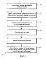
- FIG. 3is a process flow diagram showing the sequence of steps of the imprint lithography process of FIGS. 2A thru 2 E;
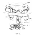
- FIG. 4shows an assembly of an orientation alignment and gap control system including both a course calibration stage and a fine orientation alignment and gap control stage according to one embodiment of the invention
- FIG. 5is an exploded view of the system of FIG. 4 ;
- FIGS. 6A and 6Bshow first and second orientation sub-stages, respectively, in the form of first and second flexure members with flexure joints according to one embodiment of the invention
- FIG. 7shows the assembled fine orientation stage with first and second flexure members coupled to each other so that their orientation axes converge on a single pivot point
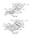
- FIG. 8is an assembly view of the course calibration stage (or pre-calibration stage) coupled to the fine orientation stage according to one embodiment
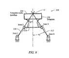
- FIG. 9is a simplified diagram of a 4-bar linkage illustrating the motion of flexure joints that result in an orientation axis
- FIG. 10illustrates a side view of the assembled orientation stage with piezo actuators
- FIGS. 11A and 11Billustrate configurations for a vacuum chuck according to the invention
- FIG. 12illustrates the method for manufacturing a vacuum chuck of the types illustrated in FIGS. 11A and 11B ;
- FIGS. 13A , 13 B and 13 Cillustrate use of the fine orientation stage to separate a template from a substrate using the “peel-and-pull” method of the present invention.
- FIGS. 14A , 14 B, and 14 Cillustrate an alternative method of separating a template from a substrate using a piezo actuator.
- the template 12predisposed with respect to a substrate 20 upon which desired features are to be imprinted using imprint lithography.
- the template 12includes a surface 14 that has been fabricated to take on the shape of desired features which, in turn, are transferred to the substrate 20 .
- a transfer layer 18Between the substrate 20 and the template 12 lies a transfer layer 18 , which receives the desired features from the template 12 via an imprinted layer 16 .
- the transfer layer 18allows one to obtain high aspect ratio structures (or features) from low aspect ratio imprinted features.
- FIG. 1Aa wedge shaped imprinted layer 16 results so that the template 12 is closer to the substrate 20 at one end of the imprinted layer 16 .
- FIG. 1Bshows the imprinted layer 16 being too thick. Both of these conditions are highly undesirable.
- the present inventionprovides a system, processes and related devices for eliminating the conditions illustrated in FIGS. 1A and 1B as well as other orientation problems associated with prior art lithography techniques.
- the template 12 and substrate 20it is necessary to maintain the template 12 and substrate 20 as close to each other as possible and nearly parallel. This requirement is very stringent as compared to other proximity lithography techniques such as proximity printing, contact printing, and X-ray lithography, as examples.
- proximity lithography techniquessuch as proximity printing, contact printing, and X-ray lithography, as examples.
- an average gap of about 200 nm or less with a variation of less than 50 nm across the imprinting area of the substrate 20is required for the imprint lithography process to be successful.
- the present inventionprovides a way of controlling the spacing between the template 12 and substrate 20 for successful imprint lithography given such tight and precise gap requirements.
- FIGS. 2A thru 2 Eillustrate the process, denoted generally as 30 , of imprint lithography according to the invention.
- the template 12is orientated in spaced relation to the substrate 20 so that a gap 31 is formed in the space separating the template 12 and substrate 20 .
- the surface 14 of template 12is treated with a thin layer 13 that lowers the template surface energy and assists in separation of the template 12 from the substrate 20 .
- the manner of orientation including devices for controlling of the gap 31 between the template 12 and substrate 20are discussed below.
- the gap 31is filled with a substance 40 that conforms to the shape of the treated surface 14 .
- the substance 40forms the imprinted layer 16 shown in FIGS. 1A and 1B .
- the substance 40is a liquid so that it fills the space of gap 31 rather easily without the use of high temperatures and the gap 31 can be closed without requiring high pressures.
- a curing agent 32shown in FIG. 2C , is applied to the template 12 causing the substance 40 to harden and assume the shape of the space defined by gap 31 between the template 12 and substrate 20 .
- desired features 44shown in FIG. 2D , from the template 12 are transferred to the upper surface of the substrate 20 .
- a transfer layer 18is provided directly on the upper surface of the substrate 20 which facilitates the amplification of features transferred from the template 12 onto the substrate 20 to generate high aspect ratio features.
- the template 12is removed from the substrate 20 leaving the desired features 44 thereon.
- the separation of the template 12 from the substrate 20must be done so that desired features 44 remain intact without shearing or tearing from the surface of the substrate 20 .
- the present inventionprovides a method and associated system for peeling and pulling (referred to herein as the “peel-and-pull” method) the template 12 from the substrate 20 following imprinting so the desired features 44 remain intact.
- FIG. 2Esummarizes the imprint lithography process, denoted generally as 50 , of the present invention in flow chart form.
- course orientation of a template and a substrateis performed so that a rough alignment of the template and substrate is achieved.
- the advantage of course orientation at step 52is that it allows pre-calibration in a manufacturing environment where numerous devices are to be manufactured with efficiency and with high production yields.
- the substratecomprises one of many die on a semiconductor wafer
- course alignmentstep 52
- step 52can be performed once on the first die and applied to all other dies during a single production run. In this way, production cycle times are reduced and yields are increased.
- the spacing between the template and substrateis controlled so that a relatively uniform gap is created between the two layers permitting the type of precise orientation required for successful imprinting.
- the present inventionprovides a device and system for achieving the type of orientation (both course and fine) required at step 54 .
- a liquidis dispensed into the gap between the template and substrate.
- the liquidis a UV curable organosilicon solution or other organic liquids that become a solid when exposed to UV light. The fact that a liquid is used eliminates the need for high temperatures and high pressures associated with prior art lithography techniques.
- the gapis closed with fine orientation of the template about the substrate and the liquid is cured resulting in a hardening of the liquid into a form having the features of the template.
- the templateis separated from the substrate, step 60 , resulting in features from the template being imprinted or transferred onto the substrate.
- the structureis etched, step 62 , using a preliminary etch to remove residual material and a well-known oxygen etching technique to etch the transfer layer.
- the present inventionprovides a system capable of achieving precise alignment and gap control in a production style fabrication process.
- the system of the present inventionprovides a pre-calibration stage for performing a preliminary and course alignment operation between the template and substrate surface to bring the relative alignment to within the motion range of a fine movement orientation stage.
- This pre-calibration stageis required only when a new template is installed into the machine (also sometimes known as a stepper) and consists of a base plate, a flexure component, and three micrometers or high resolution actuators that interconnect the base plate and the flexure component.
- FIG. 4therein is shown an assembly of the system, denoted generally as 100 , for calibrating and orienting a template, such as template 12 , shown in FIG. 1A , about a substrate to be imprinted, such as substrate 20 .
- the system 100can be utilized in a machine, such as a stepper, for mass fabrication of devices in a production type environment using the imprint lithography processes of the present invention.
- the system 100is mounted to a top frame 110 which provides support for a housing 120 which contains the pre-calibration stage for course alignment of a template 150 about a substrate (not shown in FIG. 4 ).
- the housing 120is seen coupled to a middle frame 114 with guide shafts 112 a and 112 b attached to the middle frame 114 opposite the housing 120 .
- three (3) guide shaftsare used (the back guide shaft is not visible in FIG. 4 ) to provide a support for the housing 120 as it slides up and down during vertical translation of the template 150 .
- This up-and-down motion of the housing 120is facilitated by sliders 116 a and 116 b which attach to corresponding guide shafts 112 a and 112 b about the middle frame 114 .
- System 100includes a disk-shaped base plate 122 attached to the bottom portion of the housing 120 which, in turn, is coupled to a disk-shaped flexure ring 124 for supporting the lower placed orientation stage comprised of first flexure member 126 and second flexure member 128 .
- the operation and configuration of the flexure members 126 and 128are discussed in detail below.
- the second flexure member 128is seen to include a template support 130 , which holds the template 150 in place during the imprinting process.
- the template 150comprises a piece of quartz with desired features imprinted on it, although other template substances may be used according to well-known methods.
- three (3) actuators 134 a , 134 b and 134 care fixed within the housing 120 and operable coupled to the base plate 122 and flexure ring 124 .
- the actuators 134 a , 134 b and 134 cwould be controlled such that motion of the flexure ring 124 is achieved. This allows for coarse pre-calibration.
- the actuators 134 a , 134 b and 134 ccan also be high resolution actuators which are equally spaced apart about the housing 120 permitting the additional functionality of very precise translation of the flexure ring 124 in the vertical direction to control the gap accurately.
- the system 100shown in FIG. 4 , is capable of achieving coarse orientation alignment and precise gap control of the template 150 with respect to a substrate to be imprinted.
- the system 100 of the present inventionprovides a mechanism that enables precise control of the template 150 so that precise orientation alignment is achieved and a uniform gap is maintained by the template with respect to a substrate surface. Additionally, the system 100 provides a way of separating the template 150 from the surface of the substrate following imprinting without shearing of features from the substrate surface. The precise alignment, gap control and separation features of the present invention are facilitated mainly by the configuration of the first and second flexure members, 126 and 128 , respectively.
- the first and second flexure members, 126 and 128are shown in more detail.
- the first flexure member 126is seen to include a plurality of flexure joints 160 coupled to corresponding rigid bodies 164 and 166 which form part of arms 172 and 174 extending from a frame 170 .
- the flexure frame 170has an opening 182 , which permits the penetration of a curing agent, such as UV light, to reach the template 150 , shown in FIG. 5 , when held in support 130 .
- four (4) flexure joints 160provide motion of the flexure member 126 about a first orientation axis 180 .
- the frame 170 of the first flexure member 126provides a coupling mechanism for joining with the second flexure member 128 as illustrated in FIG. 7 .
- the second flexure member 128shown in FIG. 6B , includes a pair of arms 202 and 204 extending from a frame 206 and including flexure joints 162 and corresponding rigid bodies 208 and 210 which are adapted to cause motion of the flexure member 128 about a second orientation axis 200 .
- the template support 130is integrated with the frame 206 of the second flexure member 128 and, like frame 170 , shown in FIG. 6A , has an opening 212 permitting a curing agent to reach a template 150 , shown in FIG. 5 , when held by support 130 .
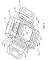
- first flexure member 126 and second flexure member 128are joined, as shown in FIG. 7 , to form the orientation stage 250 of the present invention.
- Braces 220 and 222are provided in order to facilitate joining of the two pieces such that the first orientation axis 180 , shown in FIG. 6A , and second orientation axis 200 , shown in FIG. 6E , are orthogonal to each other and intersect at a pivot point 252 at the template-substrate interface 254 .
- first orientation axis 180 and second orientation axis 200are orthogonal and lie on interface 254 provide the fine alignment and gap control advantages of the invention. Specifically, with this arrangement, a decoupling of orientation alignment from layer-to-layer overlay alignment is achieved.
- the relative position of the first orientation axis 180 and second orientation axis 200provides an orientation stage 250 that can be used to separate the template 150 from a substrate without shearing of desired features so that features transferred from the template 150 remain intact on the substrate.
- the flexure joints 160 and 162are notched shaped to provide motion of the rigid bodies 164 , 166 , 208 and 210 about pivot axes that are located along the thinnest cross section of the notches.
- This configurationprovides two (2) flexure-based sub-systems for a fine decoupled orientation stage 250 having decoupled compliant orientation axes 180 and 200 .
- the two flexure members 126 and 128are assembled via mating of surfaces such that motion of the template 150 occurs about the pivot point 252 eliminating “swinging” and other motions that would destroy or shear imprinted features from the substrate.
- the orientation stage 250can precisely move the template 150 about a pivot point 252 eliminates shearing of desired features from a substrate following imprint lithography.
- a systemlike system 100 , shown in FIG. 4 , based on the concept of the flexure components has been developed for the imprinting process described above in connection with FIGS. 2A thru 2 E.
- One of many potential application areasis the gap control and overlay alignment required in high-resolution semiconductor manufacturing.
- Another applicationmay be in the area of single layer imprint lithography for next generation hard disk manufacturing.
- Several companiesare considering such an approach to generate sub-100 nm dots on circular magnetic media. Accordingly, the invention is potentially useful in cost effective commercial fabrication of semiconductor devices and other various kinds of devices including patterned magnetic media for data storage, micro optical devices, MEMS, biological and chemical devices, X-ray optical devices, etc.
- a Z-translation stagecontrols the distance between the template 150 and substrate without providing orientation alignment.
- a pre-calibration stage 260performs a preliminary alignment operation between the template 150 and wafer surfaces to bring the relative alignment to within the motion range limits of the orientation stage 250 , shown in FIG. 7 . Pre-calibration is required only when a new template is installed into the machine.
- the pre-calibration stage 260is made of a base plate 122 , a flexure ring 124 , and actuators 134 a , 134 b and 134 c (collectively 134 ) that interconnect the base plate 122 and the flexure ring 124 via load cells 270 that measure the imprinting and separation forces in Z-direction.
- the actuators 134 a , 134 b and 134 ccan be three differential micrometers capable of expanding and contracting to cause motion of the base plate 122 and the flexure ring 124 .
- the actuators 134can be a combination of micrometer and piezo or tip-type piezo actuators such as those offered by. Physik Instruments, Inc.
- Pre-calibration of a template 150 with respect to a substratecan be performed by adjusting the actuators 134 while visually inspecting the monochromatic light induced fringe pattern appearing at the interface of the template lower surface and the substrate top surface.
- differential micrometersit has been demonstrated that two flat surfaces can be oriented parallel within 200 nm error across 1 inch using fringes obtained from green light.
- the flexure model 300includes four (4) parallel joints—Joints 1 , 2 , 3 and 4 —that provide a four-bar-linkage system in its nominal and rotated configurations.
- the angles ( 1 and 2 ) between the line 310 passing through Joints 1 and 2 and the line 312 passing thru Joints 3 and 4 , respectively,are selected so that the compliant alignment axis lies exactly on the template-wafer interface 254 within high precision machining tolerances (a few microns).
- the rigid body 314 between Joints 2 and 3rotates about an axis that is depicted by Point C.
- the rigid body 314is representative of rigid bodies 164 and 208 of the flexure members 126 and 128 , shown in FIGS. 6A and 6B , respectively.
- the resulting orientation stage 250has two decoupled orientation axes that are orthogonal to each other and lie on the template-substrate interface 254 .
- the flexure componentscan be readily adapted to have openings so that a curing UV light can pass through the template 150 as required in lithographic applications.
- the orientation stage 250is capable of fine alignment and precise motion of the template 150 with respect to a substrate and, as such, is one of the key components of the present invention.
- the second key component of the inventionis the flexure-based members 126 and 128 with flexure joints 160 and 162 which provide for no particle generation and which can be critical for the success of imprint lithography processes.
- This inventionassumes the availability of the absolute gap sensing approach that can measure small gaps of the order of 200 nm or less between the template 150 and substrate with a resolution of a few nanometers. Such gap sensing is required as feedback if gap control is to actively by use of actuators.
- FIG. 10shows a configuration of the orientation stage 250 with piezo actuators, denoted generally as 400 .
- the configuration 400generates pure tilting motions with no lateral motions at template-substrate interface 254 , shown in FIG. 7 . Therefore, a single overlay alignment step will allow the imprinting of a layer on the entire wafer.
- coupled motions between the orientation and lateral motionslead to inevitable disturbances in X-Y alignment, which requires a complicated field-to-field overlay control loop.
- the orientation stage 250possesses high stiffness in the directions where side motions or rotations are undesirable, and lower stiffness in directions where necessary orientation motions are desirable, which leads to a selectively compliant device. Therefore, the orientation stage 250 can support relatively high loads while achieving proper orientation kinematics between template 150 and the substrate.
- the template 150is made from optical flat glass using electron beam lithography to ensure that it is substantially flat on the bottom.
- the wafer substratecan exhibit a “potato chip” effect resulting in small micron-scale variations on its topography.
- the present inventionprovides a device, in the form of a vacuum chuck 478 (as shown in FIG. 12 ), to eliminate variations across a surface of the wafer substrate that can occur during imprinting.
- Vacuum chuck 478serves two primary purposes. First, vacuum chuck 478 is utilized to hold the substrate in place during imprinting and to ensure that the substrate stays flat during the imprinting process. Additionally, vacuum chuck 478 ensures that no particles are present on the back of the substrate during processing. This is important to imprint lithography as particles can create problems that ruin the device and decrease production yields.
- FIGS. 11A and 11Billustrate variations of a vacuum chuck suitable for these purposes according to two embodiments.
- a pin-type vacuum chuck 450is shown as having a large number of pins 452 that eliminates “potato chip” effect as well as other deflections on the substrate during processing.
- a vacuum channel 454is provided as a means of pulling on the substrate to keep it in place. The spacing between the pins 452 is maintained so the substrate will not bow substantially from the force applied through the vacuum channel 454 . At the same time, the tip of the pins 452 are small enough to reduce the chance of particles settling on top of it.
- pin-type vacuum chuck 450With a pin-type vacuum chuck 450 , a large number of pins 452 are used to avoid local bowing of the substrate. At the same time, the pin heads should be very small since the likelihood of the particle falling in between the gaps between the pins 452 can be high avoiding undesirable changing the shape of the substrate itself.
- FIG. 11Bshows a groove-type vacuum chuck 460 with grooves 462 across its surface.
- the multiple grooves 462perform a similar function to the pins 454 of the pin-type vacuum chuck 450 , shown in FIG. 11 A.
- the grooves 462can take on either a wall shape 464 or have a smooth curved cross section 466 .
- the cross section 466 of the grooves 462 for the groove-type vacuum chuck 460can be adjusted through an etching process.
- the space and size of each groove 462can be as small as hundreds of microns.
- Vacuum flow to each of the grooves 462can be provided typically through fine vacuum channels across multiple grooves that run in parallel with respect to the chuck surface. The fine vacuum channels can be made along with grooves through an etching process.
- FIG. 12illustrates the manufacturing process for both of the pin-type vacuum chuck 450 , shown in FIG. 11A , and the groove-type vacuum chuck 460 , shown in FIG. 11 B.
- optical flats 470no additional grinding and polishing steps are necessary for this process. Drilling at specified places of the optical flat 470 produces vacuum flow holes 472 which are then masked and patterned 474 before etching 476 to produce the desired feature—either pins or grooves—on the upper surface of the optical flat 470 .
- the surfacecan then be treated 479 using well-known methods.
- separation of the template 150 from the imprinted layeris a critical and important final step of imprint lithography. Since the template 150 and substrate are almost perfectly oriented, the assembly of the template 150 , imprinted layer, and substrate leads to a uniform contact between near optical flats, which usually requires a large separation force. In the case of a flexible template or substrate, the separation can be merely a “peeling process”. However, a flexible template or substrate is undesirable from the point of view of high-resolution overlay alignment. In case of quartz template and silicon substrate, the peeling process cannot be implemented easily.
- the separation of the template from an imprinted layercan be performed successfully either by one of the two following schemes or the combination of them as illustrated by FIGS. 13A , 13 B and 13 C.
- reference numerals 12 , 18 and 20will be used in referring to the template, transfer layer and substrate, respectively, in accordance with FIGS. 1A and 1B .
- either the template 12 or substrate 20can be tilted intentionally to induce a wedge 500 between the template 12 and transfer layer 18 on which the imprinted layer resides.
- the orientation stage 250shown in FIG. 10
- the relative lateral motion between the template 12 and substrate 20can be insignificant during the tilting motion if the tilting axis is located close to the template-substrate interface, shown in FIG. 7 .
- the template 12can be separated from the substrate 20 completely using Z-motion.
- This “peel and pull” methodresults in the desired features 44 , shown in FIG. 2E , being left intact on the transfer layer 18 and substrate 20 without undesirable shearing.
- FIGS. 14A , 148 and 14 CAn alternative method of separating the template 12 from the substrate 20 without destroying desired features 44 is illustrated by FIGS. 14A , 148 and 14 C.
- One or more piezo actuator(s) 502are installed adjacent to the template 12 , and a relative tilt can be induced between the template 12 and substrate 20 (FIG. 14 A).
- the free end of the piezo actuator 502is in contact with the substrate 20 so that when the actuator 502 is enlarged (FIG. 14 B), the template 12 can be pushed away from the substrate 20 .
- a local deformationcan induce a “peeling” and “pulling” effect between the template 12 and substrate 20 .
- the free end side of the piezo actuator 502can be surface treated similar to the treatment of the lower surface of the template 12 in order to prevent the imprinted layer from sticking to the surface of the piezo actuator 502 .
- the present inventiondiscloses a system, processes and related devices for successful imprint lithography without requiring the use of high temperatures or high pressures.
- precise control of the gap between a template and a substrate on which desired features from the template are to be transferredis achieved.
- separation of the template from the substrate (and the imprinted layer)is possible without destruction or shearing of desired features.
- the inventionalso discloses a way, in the form of suitable vacuum chucks, of holding a substrate in place during imprint lithography.
Landscapes
- Engineering & Computer Science (AREA)
- Nanotechnology (AREA)
- Physics & Mathematics (AREA)
- Chemical & Material Sciences (AREA)
- General Physics & Mathematics (AREA)
- Crystallography & Structural Chemistry (AREA)
- Theoretical Computer Science (AREA)
- Condensed Matter Physics & Semiconductors (AREA)
- Mathematical Physics (AREA)
- Manufacturing & Machinery (AREA)
- Exposure Of Semiconductors, Excluding Electron Or Ion Beam Exposure (AREA)
- Shaping Of Tube Ends By Bending Or Straightening (AREA)
- Micromachines (AREA)
Abstract
Description
Claims (27)
Priority Applications (22)
| Application Number | Priority Date | Filing Date | Title |
|---|---|---|---|
| US09/698,317US6873087B1 (en) | 1999-10-29 | 2000-10-27 | High precision orientation alignment and gap control stages for imprint lithography processes |
| EP10197359AEP2315076A1 (en) | 1999-10-29 | 2000-10-30 | A process and a system for orienting a template in imprint lithography |
| AU14488/01AAU1448801A (en) | 1999-10-29 | 2000-10-30 | High precision orientation alignment and gap control stages for imprint lithography processes |
| HK03101591.8AHK1049521A1 (en) | 1999-10-29 | 2000-10-30 | High precision orientation alignment and gap control stages for imprint lithography processes |
| PCT/US2000/030041WO2001033300A2 (en) | 1999-10-29 | 2000-10-30 | High precision orientation alignment and gap control stages for imprint lithography processes |
| JP2001535125AJP2003517727A (en) | 1999-10-29 | 2000-10-30 | High precision orientation alignment and gap control devices for imprint lithography |
| EP10197376AEP2315077A1 (en) | 1999-10-29 | 2000-10-30 | An orientation stage for achieving fine movement and alignment of a template in an imprint lithography process |
| EP00976753.4AEP1240550B1 (en) | 1999-10-29 | 2000-10-30 | A process for separating a template from a substrate during imprint lithography, and associated imprint lithography process |
| US10/617,321US6870301B2 (en) | 1999-10-29 | 2003-07-10 | Method of separating a template from a substrate during imprint lithography |
| US10/616,799US20040149687A1 (en) | 1999-10-29 | 2003-07-10 | Method of manufacturing a vacuum chuck used in imprint lithography |
| US10/775,707US6922906B2 (en) | 1999-10-29 | 2004-02-10 | Apparatus to orientate a body with respect to a surface |
| US10/785,248US6955868B2 (en) | 1999-10-29 | 2004-02-24 | Method to control the relative position between a body and a surface |
| US10/788,685US7060402B2 (en) | 1999-10-29 | 2004-02-27 | Method of orientating a template with respect to a substrate in response to a force exerted on the template |
| US10/806,956US7098572B2 (en) | 1999-10-29 | 2004-03-23 | Apparatus to control displacement of a body spaced-apart from a surface |
| US11/068,526US7432634B2 (en) | 2000-10-27 | 2005-02-28 | Remote center compliant flexure device |
| US11/118,070US7374415B2 (en) | 1999-10-29 | 2005-04-29 | Apparatus to control displacement of a body spaced-apart from a surface |
| US12/244,833US20090025246A1 (en) | 2000-10-27 | 2008-10-03 | Remote Center Compliant Flexure Device |
| US12/421,170US7701112B2 (en) | 2000-10-27 | 2009-04-09 | Remote center compliant flexure device |
| US12/718,043US20100154993A1 (en) | 2000-10-27 | 2010-03-05 | Separation methods for imprint lithography |
| JP2010161891AJP2011003910A (en) | 1999-10-29 | 2010-07-16 | Imprint lithography |
| JP2010161895AJP5603689B2 (en) | 1999-10-29 | 2010-07-16 | Imprint lithography |
| US12/915,298US20110042345A1 (en) | 2000-10-27 | 2010-10-29 | Methods for manufacturing chucking systems |
Applications Claiming Priority (2)
| Application Number | Priority Date | Filing Date | Title |
|---|---|---|---|
| US16239299P | 1999-10-29 | 1999-10-29 | |
| US09/698,317US6873087B1 (en) | 1999-10-29 | 2000-10-27 | High precision orientation alignment and gap control stages for imprint lithography processes |
Related Parent Applications (1)
| Application Number | Title | Priority Date | Filing Date |
|---|---|---|---|
| US10/616,799DivisionUS20040149687A1 (en) | 1999-10-29 | 2003-07-10 | Method of manufacturing a vacuum chuck used in imprint lithography |
Related Child Applications (7)
| Application Number | Title | Priority Date | Filing Date |
|---|---|---|---|
| US10/617,321DivisionUS6870301B2 (en) | 1999-10-29 | 2003-07-10 | Method of separating a template from a substrate during imprint lithography |
| US10/616,799DivisionUS20040149687A1 (en) | 1999-10-29 | 2003-07-10 | Method of manufacturing a vacuum chuck used in imprint lithography |
| US10/775,707DivisionUS6922906B2 (en) | 1999-10-29 | 2004-02-10 | Apparatus to orientate a body with respect to a surface |
| US10/785,248DivisionUS6955868B2 (en) | 1999-10-29 | 2004-02-24 | Method to control the relative position between a body and a surface |
| US10/788,685DivisionUS7060402B2 (en) | 1999-10-29 | 2004-02-27 | Method of orientating a template with respect to a substrate in response to a force exerted on the template |
| US10/806,956DivisionUS7098572B2 (en) | 1999-10-29 | 2004-03-23 | Apparatus to control displacement of a body spaced-apart from a surface |
| US11/068,526DivisionUS7432634B2 (en) | 1999-10-29 | 2005-02-28 | Remote center compliant flexure device |
Publications (1)
| Publication Number | Publication Date |
|---|---|
| US6873087B1true US6873087B1 (en) | 2005-03-29 |
Family
ID=26858716
Family Applications (8)
| Application Number | Title | Priority Date | Filing Date |
|---|---|---|---|
| US09/698,317Expired - LifetimeUS6873087B1 (en) | 1999-10-29 | 2000-10-27 | High precision orientation alignment and gap control stages for imprint lithography processes |
| US10/617,321Expired - LifetimeUS6870301B2 (en) | 1999-10-29 | 2003-07-10 | Method of separating a template from a substrate during imprint lithography |
| US10/616,799AbandonedUS20040149687A1 (en) | 1999-10-29 | 2003-07-10 | Method of manufacturing a vacuum chuck used in imprint lithography |
| US10/775,707Expired - LifetimeUS6922906B2 (en) | 1999-10-29 | 2004-02-10 | Apparatus to orientate a body with respect to a surface |
| US10/785,248Expired - LifetimeUS6955868B2 (en) | 1999-10-29 | 2004-02-24 | Method to control the relative position between a body and a surface |
| US10/788,685Expired - LifetimeUS7060402B2 (en) | 1999-10-29 | 2004-02-27 | Method of orientating a template with respect to a substrate in response to a force exerted on the template |
| US10/806,956Expired - Fee RelatedUS7098572B2 (en) | 1999-10-29 | 2004-03-23 | Apparatus to control displacement of a body spaced-apart from a surface |
| US11/118,070Expired - LifetimeUS7374415B2 (en) | 1999-10-29 | 2005-04-29 | Apparatus to control displacement of a body spaced-apart from a surface |
Family Applications After (7)
| Application Number | Title | Priority Date | Filing Date |
|---|---|---|---|
| US10/617,321Expired - LifetimeUS6870301B2 (en) | 1999-10-29 | 2003-07-10 | Method of separating a template from a substrate during imprint lithography |
| US10/616,799AbandonedUS20040149687A1 (en) | 1999-10-29 | 2003-07-10 | Method of manufacturing a vacuum chuck used in imprint lithography |
| US10/775,707Expired - LifetimeUS6922906B2 (en) | 1999-10-29 | 2004-02-10 | Apparatus to orientate a body with respect to a surface |
| US10/785,248Expired - LifetimeUS6955868B2 (en) | 1999-10-29 | 2004-02-24 | Method to control the relative position between a body and a surface |
| US10/788,685Expired - LifetimeUS7060402B2 (en) | 1999-10-29 | 2004-02-27 | Method of orientating a template with respect to a substrate in response to a force exerted on the template |
| US10/806,956Expired - Fee RelatedUS7098572B2 (en) | 1999-10-29 | 2004-03-23 | Apparatus to control displacement of a body spaced-apart from a surface |
| US11/118,070Expired - LifetimeUS7374415B2 (en) | 1999-10-29 | 2005-04-29 | Apparatus to control displacement of a body spaced-apart from a surface |
Country Status (6)
| Country | Link |
|---|---|
| US (8) | US6873087B1 (en) |
| EP (3) | EP2315077A1 (en) |
| JP (3) | JP2003517727A (en) |
| AU (1) | AU1448801A (en) |
| HK (1) | HK1049521A1 (en) |
| WO (1) | WO2001033300A2 (en) |
Cited By (189)
| Publication number | Priority date | Publication date | Assignee | Title |
|---|---|---|---|---|
| US20020094496A1 (en)* | 2000-07-17 | 2002-07-18 | Choi Byung J. | Method and system of automatic fluid dispensing for imprint lithography processes |
| US20030215577A1 (en)* | 2002-05-16 | 2003-11-20 | Willson Carlton Grant | Method and system for fabricating nanoscale patterns in light curable compositions using an electric field |
| US20050084804A1 (en)* | 2003-10-16 | 2005-04-21 | Molecular Imprints, Inc. | Low surface energy templates |
| US20050260295A1 (en)* | 2000-10-27 | 2005-11-24 | Board Of Regents, The University Of Texas System | Remote center compliant flexure device |
| US20050264132A1 (en)* | 1999-10-29 | 2005-12-01 | Board Of Regents, The University Of Texas System | Apparatus to control displacement of a body spaced-apart from a surface |
| US20050270312A1 (en)* | 2004-06-03 | 2005-12-08 | Molecular Imprints, Inc. | Fluid dispensing and drop-on-demand dispensing for nano-scale manufacturing |
| US20050271955A1 (en)* | 2004-06-03 | 2005-12-08 | Board Of Regents, The University Of Texas System | System and method for improvement of alignment and overlay for microlithography |
| US20050275311A1 (en)* | 2004-06-01 | 2005-12-15 | Molecular Imprints, Inc. | Compliant device for nano-scale manufacturing |
| US20050275251A1 (en)* | 2004-06-01 | 2005-12-15 | Molecular Imprints, Inc. | Compliant device for nano-scale manufacturing |
| US20060035029A1 (en)* | 2004-08-16 | 2006-02-16 | Molecular Imprints, Inc. | Method to provide a layer with uniform etch characteristics |
| US20060063112A1 (en)* | 2004-09-21 | 2006-03-23 | Molecular Imprints, Inc. | Pattern reversal employing thick residual layers |
| US20060076717A1 (en)* | 2002-07-11 | 2006-04-13 | Molecular Imprints, Inc. | Step and repeat imprint lithography processes |
| US20060077374A1 (en)* | 2002-07-11 | 2006-04-13 | Molecular Imprints, Inc. | Step and repeat imprint lithography systems |
| US20060172553A1 (en)* | 2005-01-31 | 2006-08-03 | Molecular Imprints, Inc. | Method of retaining a substrate to a wafer chuck |
| US20060177532A1 (en)* | 2005-02-04 | 2006-08-10 | Molecular Imprints, Inc. | Imprint lithography method to control extrusion of a liquid from a desired region on a substrate |
| US20060195765A1 (en)* | 2005-02-28 | 2006-08-31 | Texas Instruments Incorporated | Accelerating convergence in an iterative decoder |
| US20060193938A1 (en)* | 2005-02-25 | 2006-08-31 | Yukio Iimura | Imprinting apparatus |
| US20070031505A1 (en)* | 2005-05-06 | 2007-02-08 | Krishnendu Roy | Methods for fabricating nano and microparticles for drug delivery |
| US20070064384A1 (en)* | 2005-08-25 | 2007-03-22 | Molecular Imprints, Inc. | Method to transfer a template transfer body between a motion stage and a docking plate |
| US20070071582A1 (en)* | 2005-08-25 | 2007-03-29 | Molecular Imprints, Inc. | System to transfer a template transfer body between a motion stage and a docking plate |
| US20070074635A1 (en)* | 2005-08-25 | 2007-04-05 | Molecular Imprints, Inc. | System to couple a body and a docking plate |
| US20070126156A1 (en)* | 2005-12-01 | 2007-06-07 | Molecular Imprints, Inc. | Technique for separating a mold from solidified imprinting material |
| US20070132152A1 (en)* | 2005-12-08 | 2007-06-14 | Molecular Imprints, Inc. | Method and System for Double-Sided Patterning of Substrates |
| US20070190200A1 (en)* | 2005-01-31 | 2007-08-16 | Molecular Imprints, Inc. | Chucking system comprising an array of fluid chambers |
| US20070228593A1 (en)* | 2006-04-03 | 2007-10-04 | Molecular Imprints, Inc. | Residual Layer Thickness Measurement and Correction |
| US20070228608A1 (en)* | 2006-04-03 | 2007-10-04 | Molecular Imprints, Inc. | Preserving Filled Features when Vacuum Wiping |
| US20070243655A1 (en)* | 2006-04-18 | 2007-10-18 | Molecular Imprints, Inc. | Self-Aligned Process for Fabricating Imprint Templates Containing Variously Etched Features |
| US20070246850A1 (en)* | 2006-04-21 | 2007-10-25 | Molecular Imprints, Inc. | Method for Detecting a Particle in a Nanoimprint Lithography System |
| US20070287081A1 (en)* | 2004-06-03 | 2007-12-13 | Molecular Imprints, Inc. | Method for obtaining force combinations for template deformation using nullspace and methods optimization techniques |
| US20080070481A1 (en)* | 2006-09-15 | 2008-03-20 | Nihon Micro Coating Co., Ltd. | Probe cleaner and cleaning method |
| US20080088205A1 (en)* | 2004-05-20 | 2008-04-17 | Japan Science And Technology Agency | Method and Device for Precisely Resisting and Moving High Load |
| US20080095878A1 (en)* | 2000-10-12 | 2008-04-24 | Board Of Regents, University Of Texas System | Imprint Lithography Template Having a Feature Size Under 250 nm |
| US20080110557A1 (en)* | 2006-11-15 | 2008-05-15 | Molecular Imprints, Inc. | Methods and Compositions for Providing Preferential Adhesion and Release of Adjacent Surfaces |
| US20080153312A1 (en)* | 2004-02-18 | 2008-06-26 | Molecular Imprints, Inc. | Methods for Exposure for the Purpose of Thermal Management for Imprint Lithography Processes |
| US20080174046A1 (en)* | 2002-07-11 | 2008-07-24 | Molecular Imprints Inc. | Capillary Imprinting Technique |
| US20080209720A1 (en)* | 2005-08-12 | 2008-09-04 | Ki-Joon Kim | Method and Apparatus for Manufacturing a Probe Card |
| US20080308971A1 (en)* | 2007-06-18 | 2008-12-18 | Molecular Imprints, Inc. | Solvent-Assisted Layer Formation for Imprint Lithography |
| US20090004319A1 (en)* | 2007-05-30 | 2009-01-01 | Molecular Imprints, Inc. | Template Having a Silicon Nitride, Silicon Carbide or Silicon Oxynitride Film |
| US20090026657A1 (en)* | 2007-07-20 | 2009-01-29 | Molecular Imprints, Inc. | Alignment System and Method for a Substrate in a Nano-Imprint Process |
| US20090037004A1 (en)* | 2000-10-12 | 2009-02-05 | Molecular Imprints, Inc. | Method and System to Control Movement of a Body for Nano-Scale Manufacturing |
| US20090053535A1 (en)* | 2007-08-24 | 2009-02-26 | Molecular Imprints, Inc. | Reduced Residual Formation in Etched Multi-Layer Stacks |
| US20090130598A1 (en)* | 2007-11-21 | 2009-05-21 | Molecular Imprints, Inc. | Method of Creating a Template Employing a Lift-Off Process |
| US20090133751A1 (en)* | 2007-11-28 | 2009-05-28 | Molecular Imprints, Inc. | Nanostructured Organic Solar Cells |
| US20090140458A1 (en)* | 2007-11-21 | 2009-06-04 | Molecular Imprints, Inc. | Porous template and imprinting stack for nano-imprint lithography |
| US20090140445A1 (en)* | 2007-12-04 | 2009-06-04 | Molecular Imprints | High Throughput Imprint Based on Contact Line Motion Tracking Control |
| US20090147237A1 (en)* | 2007-12-05 | 2009-06-11 | Molecular Imprints, Inc. | Spatial Phase Feature Location |
| US20090155583A1 (en)* | 2005-07-22 | 2009-06-18 | Molecular Imprints, Inc. | Ultra-thin Polymeric Adhesion Layer |
| US20090169662A1 (en)* | 2004-11-30 | 2009-07-02 | Molecular Imprints, Inc. | Enhanced Multi Channel Alignment |
| US20090250840A1 (en)* | 2006-04-18 | 2009-10-08 | Molecular Imprints, Inc. | Template Having Alignment Marks Formed of Contrast Material |
| US20090272875A1 (en)* | 2003-06-17 | 2009-11-05 | Molecular Imprints, Inc. | Composition to Reduce Adhesion Between a Conformable Region and a Mold |
| US20090274743A1 (en)* | 2008-05-05 | 2009-11-05 | Boston Scientific Scimed, Inc. | Medical devices having a bioresorbable coating layer with a pre-determined pattern for fragmentation |
| US7670534B2 (en) | 2005-09-21 | 2010-03-02 | Molecular Imprints, Inc. | Method to control an atmosphere between a body and a substrate |
| US7670530B2 (en) | 2006-01-20 | 2010-03-02 | Molecular Imprints, Inc. | Patterning substrates employing multiple chucks |
| US20100053578A1 (en)* | 2002-07-11 | 2010-03-04 | Molecular Imprints, Inc. | Apparatus for imprint lithography using an electric field |
| US20100072671A1 (en)* | 2008-09-25 | 2010-03-25 | Molecular Imprints, Inc. | Nano-imprint lithography template fabrication and treatment |
| US7691313B2 (en) | 2002-11-13 | 2010-04-06 | Molecular Imprints, Inc. | Method for expelling gas positioned between a substrate and a mold |
| US20100084376A1 (en)* | 2008-10-02 | 2010-04-08 | Molecular Imprints, Inc. | Nano-imprint lithography templates |
| US20100090341A1 (en)* | 2008-10-14 | 2010-04-15 | Molecular Imprints, Inc. | Nano-patterned active layers formed by nano-imprint lithography |
| US20100092599A1 (en)* | 2008-10-10 | 2010-04-15 | Molecular Imprints, Inc. | Complementary Alignment Marks for Imprint Lithography |
| US20100096776A1 (en)* | 2008-10-21 | 2010-04-22 | Molecular Imprints, Inc. | Reduction of Stress During Template Separation |
| US20100098940A1 (en)* | 2008-10-20 | 2010-04-22 | Molecular Imprints, Inc. | Nano-Imprint Lithography Stack with Enhanced Adhesion Between Silicon-Containing and Non-Silicon Containing Layers |
| US20100095862A1 (en)* | 2008-10-22 | 2010-04-22 | Molecular Imprints, Inc. | Double Sidewall Angle Nano-Imprint Template |
| WO2010047788A2 (en) | 2008-10-23 | 2010-04-29 | Molecular Imprints, Inc. | Imprint lithography system and method |
| US20100102469A1 (en)* | 2008-10-24 | 2010-04-29 | Molecular Imprints, Inc. | Strain and Kinetics Control During Separation Phase of Imprint Process |
| US20100104852A1 (en)* | 2008-10-23 | 2010-04-29 | Molecular Imprints, Inc. | Fabrication of High-Throughput Nano-Imprint Lithography Templates |
| US20100102487A1 (en)* | 2008-10-28 | 2010-04-29 | Molecular Imprints, Inc. | Optical System for Use in Stage Control |
| US20100112220A1 (en)* | 2008-11-03 | 2010-05-06 | Molecular Imprints, Inc. | Dispense system set-up and characterization |
| US20100109195A1 (en)* | 2008-11-05 | 2010-05-06 | Molecular Imprints, Inc. | Release agent partition control in imprint lithography |
| US20100110434A1 (en)* | 2008-11-04 | 2010-05-06 | Molecular Imprints, Inc. | Alignment for Edge Field Nano-Imprinting |
| US20100109202A1 (en)* | 2008-11-04 | 2010-05-06 | Molecular Imprints, Inc. | Substrate Alignment |
| US20100112236A1 (en)* | 2008-10-30 | 2010-05-06 | Molecular Imprints, Inc. | Facilitating Adhesion Between Substrate and Patterned Layer |
| US20100109205A1 (en)* | 2008-11-04 | 2010-05-06 | Molecular Imprints, Inc. | Photocatalytic reactions in nano-imprint lithography processes |
| US20100173032A1 (en)* | 2007-08-09 | 2010-07-08 | Canon Kabushiki Kaisha | Imprint method and imprint apparatus |
| US7780893B2 (en) | 2006-04-03 | 2010-08-24 | Molecular Imprints, Inc. | Method of concurrently patterning a substrate having a plurality of fields and a plurality of alignment marks |
| US7785526B2 (en) | 2004-07-20 | 2010-08-31 | Molecular Imprints, Inc. | Imprint alignment method, system, and template |
| US7802978B2 (en) | 2006-04-03 | 2010-09-28 | Molecular Imprints, Inc. | Imprinting of partial fields at the edge of the wafer |
| US7811505B2 (en) | 2004-12-07 | 2010-10-12 | Molecular Imprints, Inc. | Method for fast filling of templates for imprint lithography using on template dispense |
| US20100264560A1 (en)* | 2007-12-19 | 2010-10-21 | Zhuqing Zhang | Imprint lithography apparatus and method |
| WO2010147671A1 (en) | 2009-06-19 | 2010-12-23 | Molecular Imprints, Inc. | Dual zone template chuck |
| WO2011002518A2 (en) | 2009-07-02 | 2011-01-06 | Molecular Imprints, Inc. | Chucking system with recessed support feature |
| US7880872B2 (en) | 2004-11-30 | 2011-02-01 | Molecular Imprints, Inc. | Interferometric analysis method for the manufacture of nano-scale devices |
| US20110024930A1 (en)* | 2009-07-29 | 2011-02-03 | Takashi Sato | Method of manufacturing a semiconductor device |
| US20110031650A1 (en)* | 2009-08-04 | 2011-02-10 | Molecular Imprints, Inc. | Adjacent Field Alignment |
| US20110030770A1 (en)* | 2009-08-04 | 2011-02-10 | Molecular Imprints, Inc. | Nanostructured organic solar cells |
| US20110031651A1 (en)* | 2004-01-23 | 2011-02-10 | Molecular Imprints, Inc. | Desirable wetting and release between an imprint lithography mold and a polymerizable composition |
| US20110049096A1 (en)* | 2009-08-26 | 2011-03-03 | Board Of Regents, The University Of Texas System | Functional Nanoparticles |
| US20110048518A1 (en)* | 2009-08-26 | 2011-03-03 | Molecular Imprints, Inc. | Nanostructured thin film inorganic solar cells |
| US7906058B2 (en) | 2005-12-01 | 2011-03-15 | Molecular Imprints, Inc. | Bifurcated contact printing technique |
| US20110084417A1 (en)* | 2009-10-08 | 2011-04-14 | Molecular Imprints, Inc. | Large area linear array nanoimprinting |
| WO2011066450A2 (en) | 2009-11-24 | 2011-06-03 | Molecular Imprints, Inc. | Adhesion layers in nanoimprint lithography |
| US20110140306A1 (en)* | 2004-02-27 | 2011-06-16 | Molecular Imprints, Inc. | Composition for an Etching Mask Comprising a Silicon-Containing Material |
| WO2011072202A1 (en) | 2009-12-10 | 2011-06-16 | Molecular Imprints, Inc. | Imprint lithography template |
| US20110171340A1 (en)* | 2002-07-08 | 2011-07-14 | Molecular Imprints, Inc. | Template Having a Varying Thickness to Facilitate Expelling a Gas Positioned Between a Substrate and the Template |
| US20110183070A1 (en)* | 2010-01-28 | 2011-07-28 | Molecular Imprints, Inc. | Roll-to-roll imprint lithography and purging system |
| US20110183027A1 (en)* | 2010-01-26 | 2011-07-28 | Molecular Imprints, Inc. | Micro-Conformal Templates for Nanoimprint Lithography |
| US20110183521A1 (en)* | 2010-01-27 | 2011-07-28 | Molecular Imprints, Inc. | Methods and systems of material removal and pattern transfer |
| US20110180127A1 (en)* | 2010-01-28 | 2011-07-28 | Molecular Imprints, Inc. | Solar cell fabrication by nanoimprint lithography |
| WO2011094696A2 (en) | 2010-01-29 | 2011-08-04 | Molecular Imprints, Inc. | Ultra-compliant nanoimprint lithography template |
| WO2011094672A2 (en) | 2010-01-29 | 2011-08-04 | Molecular Imprints, Inc. | Nanoimprint lithography processes for forming nanoparticles |
| WO2011097514A2 (en) | 2010-02-05 | 2011-08-11 | Molecular Imprints, Inc. | Templates having high contrast alignment marks |
| US20110193251A1 (en)* | 2010-02-09 | 2011-08-11 | Molecular Imprints, Inc. | Process Gas Confinement for Nano-Imprinting |
| US20110215503A1 (en)* | 2004-11-24 | 2011-09-08 | Molecular Imprints, Inc. | Reducing Adhesion between a Conformable Region and a Mold |
| WO2011139782A1 (en) | 2010-04-27 | 2011-11-10 | Molecular Imprints, Inc. | Separation control substrate/template for nanoimprint lithography |
| WO2012006521A1 (en) | 2010-07-08 | 2012-01-12 | Molecular Imprints, Inc. | Enhanced densification of silicon oxide layers |
| US8142703B2 (en) | 2005-10-05 | 2012-03-27 | Molecular Imprints, Inc. | Imprint lithography method |
| US8142850B2 (en) | 2006-04-03 | 2012-03-27 | Molecular Imprints, Inc. | Patterning a plurality of fields on a substrate to compensate for differing evaporation times |
| US20120152136A1 (en)* | 2009-09-02 | 2012-06-21 | Tokyo Electron Limited | Imprint method, computer storage medium and imprint apparatus |
| WO2013126750A1 (en) | 2012-02-22 | 2013-08-29 | Molecular Imprints, Inc. | Large area imprint lithography |
| US8557351B2 (en) | 2005-07-22 | 2013-10-15 | Molecular Imprints, Inc. | Method for adhering materials together |
| TWI449305B (en)* | 2011-05-17 | 2014-08-11 | Vai Nam Liu | An electromagnetic device |
| US8808808B2 (en) | 2005-07-22 | 2014-08-19 | Molecular Imprints, Inc. | Method for imprint lithography utilizing an adhesion primer layer |
| US20140242744A1 (en)* | 2011-09-26 | 2014-08-28 | Solarity, Inc. | Substrate and superstrate design and process for nano-imprinting lithography of light and carrier collection management devices |
| US8828297B2 (en) | 2010-11-05 | 2014-09-09 | Molecular Imprints, Inc. | Patterning of non-convex shaped nanostructures |
| WO2014145634A2 (en) | 2013-03-15 | 2014-09-18 | Canon Nanotechnologies, Inc. | Nano imprinting with reusable polymer template with metallic or oxide coating |
| US8850980B2 (en) | 2006-04-03 | 2014-10-07 | Canon Nanotechnologies, Inc. | Tessellated patterns in imprint lithography |
| US8891080B2 (en) | 2010-07-08 | 2014-11-18 | Canon Nanotechnologies, Inc. | Contaminate detection and substrate cleaning |
| US8889332B2 (en) | 2004-10-18 | 2014-11-18 | Canon Nanotechnologies, Inc. | Low-K dielectric functional imprinting materials |
| US8916200B2 (en) | 2010-11-05 | 2014-12-23 | Molecular Imprints, Inc. | Nanoimprint lithography formation of functional nanoparticles using dual release layers |
| US8926888B2 (en) | 2011-02-25 | 2015-01-06 | Board Of Regents, The University Of Texas System | Fluorinated silazane release agents in nanoimprint lithography |
| US8935981B2 (en) | 2010-09-24 | 2015-01-20 | Canon Nanotechnologies, Inc. | High contrast alignment marks through multiple stage imprinting |
| US8967992B2 (en) | 2011-04-25 | 2015-03-03 | Canon Nanotechnologies, Inc. | Optically absorptive material for alignment marks |
| WO2015070054A1 (en) | 2013-11-08 | 2015-05-14 | Canon Nanotechnologies, Inc. | Low contact imprint lithography template chuck system for improved overlay correction |
| WO2015089158A1 (en) | 2013-12-10 | 2015-06-18 | Canon Nanotechnologies, Inc. | Imprint lithography template and method for zero-gap imprinting |
| US9070803B2 (en) | 2010-05-11 | 2015-06-30 | Molecular Imprints, Inc. | Nanostructured solar cell |
| WO2015103232A1 (en) | 2013-12-30 | 2015-07-09 | Canon Nanotechnologies, Inc. | Methods for uniform imprint pattern transfer of sub-20 nm features |
| US9329473B2 (en) | 2010-02-15 | 2016-05-03 | Suss Microtec Lithography Gmbh | Method and device for active wedge error compensation between two objects that can be positioned substantially to parallel to each other |
| US9452574B2 (en) | 2011-12-19 | 2016-09-27 | Canon Nanotechnologies, Inc. | Fabrication of seamless large area master templates for imprint lithography using step and repeat tools |
| EP3141956A1 (en) | 2015-09-08 | 2017-03-15 | Canon Kabushiki Kaisha | Substrate pretreatment for reducing fill time in nanoimprint lithography |
| US9634163B2 (en) | 2002-06-08 | 2017-04-25 | Lccm Solar, Llc | Lateral collection photovoltaics |
| US9651862B2 (en) | 2013-07-12 | 2017-05-16 | Canon Nanotechnologies, Inc. | Drop pattern generation for imprint lithography with directionally-patterned templates |
| US9902640B2 (en) | 2012-06-28 | 2018-02-27 | Corning Incorporated | Process and system tuning precision glass sheet bending |
| US9971249B1 (en) | 2017-02-27 | 2018-05-15 | Canon Kabushiki Kaisha | Method and system for controlled ultraviolet light exposure |
| US9993962B2 (en) | 2016-05-23 | 2018-06-12 | Canon Kabushiki Kaisha | Method of imprinting to correct for a distortion within an imprint system |
| US10035296B2 (en) | 2016-10-13 | 2018-07-31 | Canon Kabushiki Kaisha | Methods for controlling spread of imprint material |
| US10079152B1 (en) | 2017-02-24 | 2018-09-18 | Canon Kabushiki Kaisha | Method for forming planarized etch mask structures over existing topography |
| US10095106B2 (en) | 2016-03-31 | 2018-10-09 | Canon Kabushiki Kaisha | Removing substrate pretreatment compositions in nanoimprint lithography |
| US10131134B2 (en) | 2015-10-30 | 2018-11-20 | Canon Kabushiki Kaisha | System and method for discharging electrostatic charge in nanoimprint lithography processes |
| US10134588B2 (en) | 2016-03-31 | 2018-11-20 | Canon Kabushiki Kaisha | Imprint resist and substrate pretreatment for reducing fill time in nanoimprint lithography |
| US10156725B2 (en) | 2014-09-29 | 2018-12-18 | Magic Leap, Inc. | Architectures and methods for outputting different wavelength light out of waveguides |
| US10189188B2 (en) | 2016-05-20 | 2019-01-29 | Canon Kabushiki Kaisha | Nanoimprint lithography adhesion layer |
| US10211051B2 (en) | 2015-11-13 | 2019-02-19 | Canon Kabushiki Kaisha | Method of reverse tone patterning |
| US10254454B2 (en) | 2015-06-15 | 2019-04-09 | Magic Leap, Inc. | Display system with optical elements for in-coupling multiplexed light streams |
| US10303049B2 (en) | 2017-03-22 | 2019-05-28 | Canon Kabushiki Kaisha | Reducing electric charge in imprint lithography |
| US10317793B2 (en) | 2017-03-03 | 2019-06-11 | Canon Kabushiki Kaisha | Substrate pretreatment compositions for nanoimprint lithography |
| US10371896B2 (en) | 2016-12-22 | 2019-08-06 | Magic Leap, Inc. | Color separation in planar waveguides using dichroic filters |
| US10488753B2 (en) | 2015-09-08 | 2019-11-26 | Canon Kabushiki Kaisha | Substrate pretreatment and etch uniformity in nanoimprint lithography |
| US10509313B2 (en) | 2016-06-28 | 2019-12-17 | Canon Kabushiki Kaisha | Imprint resist with fluorinated photoinitiator and substrate pretreatment for reducing fill time in nanoimprint lithography |
| US10534259B2 (en) | 2017-03-28 | 2020-01-14 | Canon Kabushiki Kaisha | Method and system for imprint force control |
| US10578964B2 (en) | 2013-12-31 | 2020-03-03 | Canon Nanotechnologies, Inc. | Asymmetric template shape modulation for partial field imprinting |
| US10578984B2 (en) | 2016-12-20 | 2020-03-03 | Canon Kabushiki Kaisha | Adaptive chucking system |
| US20200073228A1 (en)* | 2018-08-30 | 2020-03-05 | Toshiba Memory Corporation | Original plate |
| US10620539B2 (en) | 2016-03-31 | 2020-04-14 | Canon Kabushiki Kaisha | Curing substrate pretreatment compositions in nanoimprint lithography |
| US10627715B2 (en) | 2016-10-31 | 2020-04-21 | Canon Kabushiki Kaisha | Method for separating a nanoimprint template from a substrate |
| US10654216B2 (en) | 2016-03-30 | 2020-05-19 | Canon Kabushiki Kaisha | System and methods for nanoimprint lithography |
| US10712660B2 (en) | 2016-12-21 | 2020-07-14 | Canon Kabushiki Kaisha | Template for imprint lithography including a recession and an apparatus and method of using the template |
| US10866510B2 (en)* | 2017-07-31 | 2020-12-15 | Canon Kabushiki Kaisha | Overlay improvement in nanoimprint lithography |
| US10895784B2 (en) | 2016-12-14 | 2021-01-19 | Magic Leap, Inc. | Patterning of liquid crystals using soft-imprint replication of surface alignment patterns |
| US10908423B2 (en) | 2016-11-18 | 2021-02-02 | Magic Leap, Inc. | Multilayer liquid crystal diffractive gratings for redirecting light of wide incident angle ranges |
| US10921630B2 (en) | 2016-11-18 | 2021-02-16 | Magic Leap, Inc. | Spatially variable liquid crystal diffraction gratings |
| US10935884B2 (en) | 2017-03-08 | 2021-03-02 | Canon Kabushiki Kaisha | Pattern forming method and methods for manufacturing processed substrate, optical component and quartz mold replica as well as coating material for imprint pretreatment and set thereof with imprint resist |
| US10935883B2 (en) | 2017-09-29 | 2021-03-02 | Canon Kabushiki Kaisha | Nanoimprint template with light blocking material and method of fabrication |
| US10962855B2 (en) | 2017-02-23 | 2021-03-30 | Magic Leap, Inc. | Display system with variable power reflector |
| US10969680B2 (en) | 2016-11-30 | 2021-04-06 | Canon Kabushiki Kaisha | System and method for adjusting a position of a template |
| US10969588B2 (en) | 2015-03-16 | 2021-04-06 | Magic Leap, Inc. | Methods and systems for diagnosing contrast sensitivity |
| US10976632B2 (en) | 2016-12-08 | 2021-04-13 | Magic Leap, Inc. | Diffractive devices based on cholesteric liquid crystal |
| US10991582B2 (en) | 2016-12-21 | 2021-04-27 | Canon Kabushiki Kaisha | Template for imprint lithography including a recession, an apparatus of using the template, and a method of fabricating an article |
| US20210125855A1 (en)* | 2019-10-29 | 2021-04-29 | Canon Kabushiki Kaisha | Superstrate chuck, method of use, and method of manufacturing an article |
| US10996561B2 (en) | 2017-12-26 | 2021-05-04 | Canon Kabushiki Kaisha | Nanoimprint lithography with a six degrees-of-freedom imprint head module |
| US10996560B2 (en) | 2017-07-31 | 2021-05-04 | Canon Kabushiki Kaisha | Real-time correction of template deformation in nanoimprint lithography |
| US11037785B2 (en) | 2017-03-08 | 2021-06-15 | Canon Kabushiki Kaisha | Method for fabricating pattern of cured product and methods for manufacturing optical component, circuit board and quartz mold replica as well as coating material for imprint pretreatment and cured product thereof |
| US11067860B2 (en) | 2016-11-18 | 2021-07-20 | Magic Leap, Inc. | Liquid crystal diffractive devices with nano-scale pattern and methods of manufacturing the same |
| US11073695B2 (en) | 2017-03-21 | 2021-07-27 | Magic Leap, Inc. | Eye-imaging apparatus using diffractive optical elements |
| US11086125B2 (en) | 2016-05-12 | 2021-08-10 | Magic Leap, Inc. | Distributed light manipulation over imaging waveguide |
| US11104057B2 (en) | 2015-12-11 | 2021-08-31 | Canon Kabushiki Kaisha | Imprint apparatus and method of imprinting a partial field |
| US11106041B2 (en) | 2016-04-08 | 2021-08-31 | Magic Leap, Inc. | Augmented reality systems and methods with variable focus lens elements |
| US11131922B2 (en) | 2016-06-06 | 2021-09-28 | Canon Kabushiki Kaisha | Imprint lithography template, system, and method of imprinting |
| US11204462B2 (en) | 2017-01-23 | 2021-12-21 | Magic Leap, Inc. | Eyepiece for virtual, augmented, or mixed reality systems |
| US11237393B2 (en) | 2018-11-20 | 2022-02-01 | Magic Leap, Inc. | Eyepieces for augmented reality display system |
| US11347063B2 (en) | 2017-12-15 | 2022-05-31 | Magic Leap, Inc. | Eyepieces for augmented reality display system |
| US11378864B2 (en) | 2016-11-18 | 2022-07-05 | Magic Leap, Inc. | Waveguide light multiplexer using crossed gratings |
| US11454883B2 (en) | 2016-11-14 | 2022-09-27 | Canon Kabushiki Kaisha | Template replication |
| US20230001608A1 (en)* | 2021-06-30 | 2023-01-05 | Canon Kabushiki Kaisha | Conveyance apparatus, planarization apparatus, and article manufacturing method |
| US20230061361A1 (en)* | 2020-01-31 | 2023-03-02 | Canon Kabushiki Kaisha | Planarization apparatus, planarization process, and method of manufacturing an article |
| US11635684B1 (en) | 2022-03-30 | 2023-04-25 | Canon Kabushiki Kaisha | Apparatus for imprint lithography configured to generate a fluid droplet pattern and a method of using such apparatus |
| US11650423B2 (en) | 2019-06-20 | 2023-05-16 | Magic Leap, Inc. | Eyepieces for augmented reality display system |
| US11815811B2 (en) | 2021-03-23 | 2023-11-14 | Canon Kabushiki Kaisha | Magnification ramp scheme to mitigate template slippage |
| US11841481B2 (en) | 2017-09-21 | 2023-12-12 | Magic Leap, Inc. | Augmented reality display with waveguide configured to capture images of eye and/or environment |
| US12124165B2 (en) | 2021-10-25 | 2024-10-22 | Canon Kabushiki Kaisha | Apparatus and method for optimizing actuator forces |
| US12195382B2 (en) | 2021-12-01 | 2025-01-14 | Canon Kabushiki Kaisha | Superstrate and a method of using the same |
Families Citing this family (119)
| Publication number | Priority date | Publication date | Assignee | Title |
|---|---|---|---|---|
| US6334960B1 (en) | 1999-03-11 | 2002-01-01 | Board Of Regents, The University Of Texas System | Step and flash imprint lithography |
| AU2001273491A1 (en) | 2000-07-16 | 2002-02-05 | Board Of Regents, The University Of Texas System | High-resolution overlay alignment methods and systems for imprint lithography |
| US20080164638A1 (en)* | 2006-11-28 | 2008-07-10 | Wei Zhang | Method and apparatus for rapid imprint lithography |
| JP2004505273A (en) | 2000-08-01 | 2004-02-19 | ボード・オブ・リージエンツ,ザ・ユニバーシテイ・オブ・テキサス・システム | Method for highly accurate sensing of gap and orientation between transparent template and substrate for transfer lithography |
| AU2001286573A1 (en)* | 2000-08-21 | 2002-03-04 | Board Of Regents, The University Of Texas System | Flexure based macro motion translation stage |
| US6974604B2 (en) | 2001-09-28 | 2005-12-13 | Hrl Laboratories, Llc | Method of self-latching for adhesion during self-assembly of electronic or optical components |
| US7253091B2 (en) | 2001-09-28 | 2007-08-07 | Hrl Laboratories, Llc | Process for assembling three-dimensional systems on a chip and structure thus obtained |
| US7018575B2 (en) | 2001-09-28 | 2006-03-28 | Hrl Laboratories, Llc | Method for assembly of complementary-shaped receptacle site and device microstructures |
| WO2003030252A2 (en)* | 2001-09-28 | 2003-04-10 | Hrl Laboratories, Llc | Process for producing interconnects |
| US7117790B2 (en)* | 2002-01-11 | 2006-10-10 | Massachusetts Institute Of Technology | Microcontact printing |
| JP4372683B2 (en) | 2002-06-07 | 2009-11-25 | オブデュキャット、アクチボラグ | Pattern transfer method |
| MY164487A (en)* | 2002-07-11 | 2017-12-29 | Molecular Imprints Inc | Step and repeat imprint lithography processes |
| US6932934B2 (en) | 2002-07-11 | 2005-08-23 | Molecular Imprints, Inc. | Formation of discontinuous films during an imprint lithography process |
| US6916584B2 (en) | 2002-08-01 | 2005-07-12 | Molecular Imprints, Inc. | Alignment methods for imprint lithography |
| WO2004013693A2 (en)* | 2002-08-01 | 2004-02-12 | Molecular Imprints, Inc. | Scatterometry alignment for imprint lithography |
| US7071088B2 (en) | 2002-08-23 | 2006-07-04 | Molecular Imprints, Inc. | Method for fabricating bulbous-shaped vias |
| US6887792B2 (en)* | 2002-09-17 | 2005-05-03 | Hewlett-Packard Development Company, L.P. | Embossed mask lithography |
| US8349241B2 (en) | 2002-10-04 | 2013-01-08 | Molecular Imprints, Inc. | Method to arrange features on a substrate to replicate features having minimal dimensional variability |
| US6929762B2 (en) | 2002-11-13 | 2005-08-16 | Molecular Imprints, Inc. | Method of reducing pattern distortions during imprint lithography processes |
| US7641840B2 (en)* | 2002-11-13 | 2010-01-05 | Molecular Imprints, Inc. | Method for expelling gas positioned between a substrate and a mold |
| GB0227902D0 (en)* | 2002-11-29 | 2003-01-08 | Ingenia Holdings Ltd | Template |
| US6871558B2 (en) | 2002-12-12 | 2005-03-29 | Molecular Imprints, Inc. | Method for determining characteristics of substrate employing fluid geometries |
| US7452574B2 (en) | 2003-02-27 | 2008-11-18 | Molecular Imprints, Inc. | Method to reduce adhesion between a polymerizable layer and a substrate employing a fluorine-containing layer |
| US7122079B2 (en) | 2004-02-27 | 2006-10-17 | Molecular Imprints, Inc. | Composition for an etching mask comprising a silicon-containing material |
| US7157036B2 (en) | 2003-06-17 | 2007-01-02 | Molecular Imprints, Inc | Method to reduce adhesion between a conformable region and a pattern of a mold |
| US7223635B1 (en) | 2003-07-25 | 2007-05-29 | Hrl Laboratories, Llc | Oriented self-location of microstructures with alignment structures |
| US7136150B2 (en) | 2003-09-25 | 2006-11-14 | Molecular Imprints, Inc. | Imprint lithography template having opaque alignment marks |
| JP3889386B2 (en)* | 2003-09-30 | 2007-03-07 | 株式会社東芝 | Imprint apparatus and imprint method |
| US7090716B2 (en)* | 2003-10-02 | 2006-08-15 | Molecular Imprints, Inc. | Single phase fluid imprint lithography method |
| JP2005153113A (en)* | 2003-11-28 | 2005-06-16 | Ricoh Opt Ind Co Ltd | Method for manufacturing fine three-dimensional structure by means of nano-printing and fine three-dimensional structure |
| EP1538482B1 (en) | 2003-12-05 | 2016-02-17 | Obducat AB | Device and method for large area lithography |
| KR100585951B1 (en)* | 2004-02-18 | 2006-06-01 | 한국기계연구원 | Imprinting device with multiple modules that can be combined / separate independent drive |
| US8076386B2 (en) | 2004-02-23 | 2011-12-13 | Molecular Imprints, Inc. | Materials for imprint lithography |
| WO2005093737A1 (en)* | 2004-03-29 | 2005-10-06 | Pioneer Corporation | Pattern transfer apparatus and pattern transfer method |
| DE102004028851B4 (en)* | 2004-03-31 | 2006-04-13 | Infineon Technologies Ag | Method and device for measuring a surface profile of a sample |
| EP1594001B1 (en) | 2004-05-07 | 2015-12-30 | Obducat AB | Device and method for imprint lithography |
| WO2005119802A2 (en) | 2004-05-28 | 2005-12-15 | Board Of Regents, The University Of Texas System | Adaptive shape substrate support system and method |
| JP4574240B2 (en)* | 2004-06-11 | 2010-11-04 | キヤノン株式会社 | Processing apparatus, processing method, device manufacturing method |
| JP4458958B2 (en)* | 2004-07-01 | 2010-04-28 | 独立行政法人理化学研究所 | Fine pattern forming method and fine pattern forming apparatus |
| US20060017876A1 (en)* | 2004-07-23 | 2006-01-26 | Molecular Imprints, Inc. | Displays and method for fabricating displays |
| US7105452B2 (en)* | 2004-08-13 | 2006-09-12 | Molecular Imprints, Inc. | Method of planarizing a semiconductor substrate with an etching chemistry |
| US7492440B2 (en)* | 2004-09-09 | 2009-02-17 | Asml Netherlands B.V. | Lithographic apparatus and device manufacturing method |
| JP4904742B2 (en)* | 2004-09-16 | 2012-03-28 | 旭硝子株式会社 | Pattern forming method and article having pattern |
| JP4979918B2 (en)* | 2004-09-24 | 2012-07-18 | ボンドテック株式会社 | Pressurizing method and pressurizing apparatus |
| US7244386B2 (en) | 2004-09-27 | 2007-07-17 | Molecular Imprints, Inc. | Method of compensating for a volumetric shrinkage of a material disposed upon a substrate to form a substantially planar structure therefrom |
| CN100395121C (en)* | 2004-11-19 | 2008-06-18 | 鸿富锦精密工业(深圳)有限公司 | hot embossing method |
| WO2006060757A2 (en)* | 2004-12-01 | 2006-06-08 | Molecular Imprints, Inc. | Eliminating printability of sub-resolution defects in imprint lithography |
| US7295288B1 (en)* | 2004-12-01 | 2007-11-13 | Advanced Micro Devices, Inc. | Systems and methods of imprint lithography with adjustable mask |
| JP2006165371A (en)* | 2004-12-09 | 2006-06-22 | Canon Inc | Transfer apparatus and device manufacturing method |
| US7410591B2 (en)* | 2004-12-16 | 2008-08-12 | Asml Holding N.V. | Method and system for making a nano-plate for imprint lithography |
| US7409759B2 (en)* | 2004-12-16 | 2008-08-12 | Asml Holding N.V. | Method for making a computer hard drive platen using a nano-plate |
| US7331283B2 (en)* | 2004-12-16 | 2008-02-19 | Asml Holding N.V. | Method and apparatus for imprint pattern replication |
| US7399422B2 (en)* | 2005-11-29 | 2008-07-15 | Asml Holding N.V. | System and method for forming nanodisks used in imprint lithography and nanodisk and memory disk formed thereby |
| US7363854B2 (en)* | 2004-12-16 | 2008-04-29 | Asml Holding N.V. | System and method for patterning both sides of a substrate utilizing imprint lithography |
| US7676088B2 (en)* | 2004-12-23 | 2010-03-09 | Asml Netherlands B.V. | Imprint lithography |
| KR100688866B1 (en) | 2005-04-07 | 2007-03-02 | 삼성전기주식회사 | Imprint device, system and method |
| JP4595120B2 (en)* | 2005-05-27 | 2010-12-08 | 独立行政法人産業技術総合研究所 | Imprint method and apparatus by back surface pressurization |
| GB2426486A (en)* | 2005-05-27 | 2006-11-29 | Microsaic Systems Ltd | Self-aligning micro-contact print engine |
| JP3958344B2 (en) | 2005-06-07 | 2007-08-15 | キヤノン株式会社 | Imprint apparatus, imprint method, and chip manufacturing method |
| JP4290177B2 (en) | 2005-06-08 | 2009-07-01 | キヤノン株式会社 | Mold, alignment method, pattern forming apparatus, pattern transfer apparatus, and chip manufacturing method |
| EP1949147B1 (en)* | 2005-11-18 | 2012-03-21 | Nanocomp Oy Ltd. | Method of producing a diffraction grating element |
| KR101293059B1 (en)* | 2005-12-08 | 2013-08-05 | 몰레큘러 임프린츠 인코퍼레이티드 | Method for expelling gas positioned between a substrate and a mold |
| US7517211B2 (en) | 2005-12-21 | 2009-04-14 | Asml Netherlands B.V. | Imprint lithography |
| KR100898793B1 (en)* | 2005-12-29 | 2009-05-20 | 엘지디스플레이 주식회사 | Substrate bonding device for liquid crystal display device |
| US8015510B2 (en) | 2006-02-17 | 2011-09-06 | Mentor Graphics Corporation | Interconnection modeling for semiconductor fabrication process effects |
| JP4845564B2 (en)* | 2006-03-31 | 2011-12-28 | 株式会社東芝 | Pattern transfer method |
| KR20080114681A (en)* | 2006-04-03 | 2008-12-31 | 몰레큘러 임프린츠 인코퍼레이티드 | Lithography Imprinting System |
| JP2007329276A (en) | 2006-06-07 | 2007-12-20 | Tokyo Ohka Kogyo Co Ltd | Method for forming resist pattern by nanoimprint lithography |
| JP4810319B2 (en)* | 2006-06-09 | 2011-11-09 | キヤノン株式会社 | Processing apparatus and device manufacturing method |
| JP4939134B2 (en)* | 2006-07-07 | 2012-05-23 | 株式会社日立ハイテクノロジーズ | Imprint apparatus and imprint method |
| US20080090312A1 (en)* | 2006-10-17 | 2008-04-17 | Inkyu Park | LITHOGRAPHY ALIGNMENT SYSTEM AND METHOD USING nDSE-BASED FEEDBACK CONTROL |
| GB2444322B (en)* | 2006-11-30 | 2009-03-04 | Cinetic Landis Grinding Ltd | Apparatus for applying a controlled force to an article |
| JP4478164B2 (en)* | 2007-03-12 | 2010-06-09 | 株式会社日立ハイテクノロジーズ | MICROSTRUCTURE TRANSFER APPARATUS, STAMPER, AND MICROSTRUCTURE MANUFACTURING METHOD |
| KR20080096901A (en)* | 2007-04-30 | 2008-11-04 | 삼성전자주식회사 | Imprint method and display board manufacturing method using the imprint method |
| US20090014917A1 (en)* | 2007-07-10 | 2009-01-15 | Molecular Imprints, Inc. | Drop Pattern Generation for Imprint Lithography |
| US7490797B1 (en)* | 2007-07-26 | 2009-02-17 | Hung Hi Law | Portable supporting apparatus |
| US8119052B2 (en)* | 2007-11-02 | 2012-02-21 | Molecular Imprints, Inc. | Drop pattern generation for imprint lithography |
| USD604352S1 (en)* | 2007-11-08 | 2009-11-17 | Gitzo S.A. | Quick release attachment device for a support head of video and photographic apparatus |
| US7815824B2 (en)* | 2008-02-26 | 2010-10-19 | Molecular Imprints, Inc. | Real time imprint process diagnostics for defects |
| US8210840B2 (en)* | 2008-04-17 | 2012-07-03 | Massachusetts Institute Of Technology | Diaphragm flexure with large range and high load capacity |
| WO2009129441A2 (en)* | 2008-04-17 | 2009-10-22 | Massachusetts Institute Of Technology | Symmetric thermocentric flexure with minimal yaw error motion |
| US8512797B2 (en)* | 2008-10-21 | 2013-08-20 | Molecular Imprints, Inc. | Drop pattern generation with edge weighting |
| US8586126B2 (en) | 2008-10-21 | 2013-11-19 | Molecular Imprints, Inc. | Robust optimization to generate drop patterns in imprint lithography which are tolerant of variations in drop volume and drop placement |
| US8309008B2 (en)* | 2008-10-30 | 2012-11-13 | Molecular Imprints, Inc. | Separation in an imprint lithography process |
| JP4944158B2 (en)* | 2009-06-01 | 2012-05-30 | 株式会社日立製作所 | Nanoprinting stamper and fine structure transfer method |
| JP5295870B2 (en)* | 2009-06-02 | 2013-09-18 | 株式会社東芝 | Imprint pattern forming method |
| US8146262B1 (en) | 2009-10-21 | 2012-04-03 | The Boeing Company | Method and device for locating hole center |
| JP5669377B2 (en)* | 2009-11-09 | 2015-02-12 | キヤノン株式会社 | Imprint apparatus and article manufacturing method |
| WO2012007522A2 (en)* | 2010-07-15 | 2012-01-19 | Replisaurus Group Sas | Separation of master electrode and substrate in ecpr |
| EP2612109B1 (en)* | 2010-09-03 | 2014-06-04 | Ev Group E. Thallner GmbH | Device and method for reducing a wedge error |
| JP5661666B2 (en) | 2012-02-29 | 2015-01-28 | 株式会社東芝 | Pattern forming apparatus and semiconductor device manufacturing method |
| US9370865B1 (en)* | 2012-05-23 | 2016-06-21 | Western Digital Technologies, Inc. | Flexure based compliance device for use with an assembly device |
| JP6019953B2 (en)* | 2012-09-04 | 2016-11-02 | 大日本印刷株式会社 | Convex structure manufacturing method and manufacturing system |
| US8813382B1 (en)* | 2012-10-22 | 2014-08-26 | The Boeing Company | Shim measurement system and method of operating the same |
| WO2014145360A1 (en)* | 2013-03-15 | 2014-09-18 | Nanonex Corporation | Imprint lithography system and method for manufacturing |
| WO2014145826A2 (en)* | 2013-03-15 | 2014-09-18 | Nanonex Corporation | System and methods of mold/substrate separation for imprint lithography |
| RU2546989C2 (en)* | 2013-08-01 | 2015-04-10 | Федеральное государственное бюджетное учреждение науки Институт ядерной физики им. Г.И. Будкера Сибирского отделения РАН (ИЯФ СО РАН) | X-ray mask and method of its fabrication |
| US9341290B2 (en)* | 2014-09-29 | 2016-05-17 | Dieterich Standard, Inc. | Lugged wafer alignment ring |
| JP6525567B2 (en)* | 2014-12-02 | 2019-06-05 | キヤノン株式会社 | Imprint apparatus and method of manufacturing article |
| JP6478635B2 (en)* | 2015-01-05 | 2019-03-06 | キヤノン株式会社 | Imprint apparatus, imprint method, and article manufacturing method |
| WO2017066546A1 (en) | 2015-10-15 | 2017-04-20 | Board Of Regents, The University Of Texas System | Versatile process for precision nanoscale manufacturing |
| WO2019067928A2 (en) | 2017-09-29 | 2019-04-04 | Nike Innovate C.V. | Structurally-colored articles and methods of making and using structurally-colored articles |
| CN108198752A (en)* | 2017-12-29 | 2018-06-22 | 长沙新材料产业研究院有限公司 | A kind of method for preparing pattern on substrate |
| JP7100485B2 (en)* | 2018-04-26 | 2022-07-13 | キヤノン株式会社 | Imprint device and device manufacturing method |
| US11249405B2 (en)* | 2018-04-30 | 2022-02-15 | Canon Kabushiki Kaisha | System and method for improving the performance of a nanoimprint system |
| US10513135B1 (en) | 2018-06-15 | 2019-12-24 | Elizabeth A. Gessner | Stamping tool accessory and stamping tool assembly including the same |
| NL2023051B1 (en)* | 2019-05-02 | 2020-11-23 | Suss Microtec Lithography Gmbh | Framework for a replication device, replication device as well as method for producing nanostructured and/or microstructured components by means of a 5 replication device |
| NL2023097B1 (en) | 2019-05-09 | 2020-11-30 | Suss Microtec Lithography Gmbh | Stamp replication device and method for producing a holding means for a stamp replication device as well as a stamp |
| WO2020263362A1 (en) | 2019-06-26 | 2020-12-30 | Nike Innovate C.V. | Structurally-colored articles and methods for making and using structurally-colored articles |
| US20210022444A1 (en) | 2019-07-26 | 2021-01-28 | Nike, Inc. | Structurally-colored articles and methods for making and using structurally-colored articles |
| US11986042B2 (en) | 2019-10-21 | 2024-05-21 | Nike, Inc. | Structurally-colored articles and methods for making and using structurally-colored articles |
| US20210373213A1 (en) | 2020-05-29 | 2021-12-02 | Nike, Inc. | Structurally-colored articles and methods for making and using structurally-colored articles |
| US11241062B1 (en) | 2020-08-07 | 2022-02-08 | Nike, Inc. | Footwear article having repurposed material with structural-color concealing layer |
| US11889894B2 (en) | 2020-08-07 | 2024-02-06 | Nike, Inc. | Footwear article having concealing layer |
| US11129444B1 (en)* | 2020-08-07 | 2021-09-28 | Nike, Inc. | Footwear article having repurposed material with concealing layer |
| TWI888630B (en)* | 2020-09-01 | 2025-07-01 | 美商伊路米納有限公司 | Fixtures and related systems and methods |
| KR102442459B1 (en)* | 2020-10-07 | 2022-09-14 | 주식회사 오럼머티리얼 | Producing method of template for supporting mask and template for supporting mask and producing method of mask integrated frame |
| US11562984B1 (en) | 2020-10-14 | 2023-01-24 | Hrl Laboratories, Llc | Integrated mechanical aids for high accuracy alignable-electrical contacts |
| US12057429B1 (en) | 2021-06-23 | 2024-08-06 | Hrl Laboratories, Llc | Temporary bonding structures for die-to-die and wafer-to-wafer bonding |
Citations (159)
| Publication number | Priority date | Publication date | Assignee | Title |
|---|---|---|---|---|
| US3527062A (en)* | 1968-09-25 | 1970-09-08 | Singer General Precision | Universal joint flexure hinge |
| US3783520A (en)* | 1970-09-28 | 1974-01-08 | Bell Telephone Labor Inc | High accuracy alignment procedure utilizing moire patterns |
| US3807027A (en) | 1972-03-31 | 1974-04-30 | Johns Manville | Method of forming the bell end of a bell and spigot joint |
| US3807029A (en) | 1972-09-05 | 1974-04-30 | Bendix Corp | Method of making a flexural pivot |
| US3811665A (en) | 1972-09-05 | 1974-05-21 | Bendix Corp | Flexural pivot with diaphragm means |
| US4062600A (en) | 1976-04-05 | 1977-12-13 | Litton Systems, Inc. | Dual-gimbal gyroscope flexure suspension |
| US4070116A (en) | 1975-06-23 | 1978-01-24 | International Business Machines Corporation | Gap measuring device for defining the distance between two or more surfaces |
| US4098001A (en) | 1976-10-13 | 1978-07-04 | The Charles Stark Draper Laboratory, Inc. | Remote center compliance system |
| DE2800476A1 (en) | 1977-01-07 | 1978-07-13 | Instruments Sa | Mass prodn. method for grids, graticules etc. - using revolving drum, belt carrying resin and UV light source for polymerisation process |
| US4119688A (en) | 1975-11-03 | 1978-10-10 | International Business Machines Corporation | Electro-lithography method |
| US4155169A (en) | 1978-03-16 | 1979-05-22 | The Charles Stark Draper Laboratory, Inc. | Compliant assembly system device |
| US4202107A (en) | 1978-10-23 | 1980-05-13 | Watson Paul C | Remote axis admittance system |
| JPS5588332U (en) | 1978-12-05 | 1980-06-18 | ||
| US4267212A (en) | 1978-09-20 | 1981-05-12 | Fuji Photo Film Co., Ltd. | Spin coating process |
| JPS577931B2 (en) | 1972-12-23 | 1982-02-13 | ||
| US4326805A (en) | 1980-04-11 | 1982-04-27 | Bell Telephone Laboratories, Incorporated | Method and apparatus for aligning mask and wafer members |
| US4337579A (en) | 1980-04-16 | 1982-07-06 | The Charles Stark Draper Laboratory, Inc. | Deformable remote center compliance device |
| US4355469A (en) | 1980-11-28 | 1982-10-26 | The Charles Stark Draper Laboratory, Inc. | Folded remote center compliance device |
| US4414750A (en) | 1981-10-19 | 1983-11-15 | The Charles Stark Draper Laboratory, Inc. | Single stage remote center compliance device |
| US4440804A (en) | 1982-08-02 | 1984-04-03 | Fairchild Camera & Instrument Corporation | Lift-off process for fabricating self-aligned contacts |
| US4451507A (en) | 1982-10-29 | 1984-05-29 | Rca Corporation | Automatic liquid dispensing apparatus for spinning surface of uniform thickness |
| US4544572A (en) | 1982-09-07 | 1985-10-01 | Minnesota Mining And Manufacturing Company | Coated ophthalmic lenses and method for coating the same |
| US4600309A (en) | 1982-12-30 | 1986-07-15 | Thomson-Csf | Process and apparatus for theoptical alignment of patterns in two close-up planes in an exposure means incorporating a divergent radiation source |
| US4610442A (en) | 1982-10-19 | 1986-09-09 | Matsushita Electric Industrial Co, Ltd. | Positioning table |
| US4694703A (en) | 1984-06-28 | 1987-09-22 | Lear Siegler, Inc. | Circumferentially oriented flexure suspension |
| US4724222A (en) | 1986-04-28 | 1988-02-09 | American Telephone And Telegraph Company, At&T Bell Laboratories | Wafer chuck comprising a curved reference surface |
| US4731155A (en) | 1987-04-15 | 1988-03-15 | General Electric Company | Process for forming a lithographic mask |
| US4763886A (en) | 1986-12-26 | 1988-08-16 | Nippon Thompson Co., Ltd. | XY-positioning table |
| JPS63138730U (en) | 1987-03-03 | 1988-09-13 | ||
| US4848911A (en) | 1986-06-11 | 1989-07-18 | Kabushiki Kaisha Toshiba | Method for aligning first and second objects, relative to each other, and apparatus for practicing this method |
| JPH01196749A (en) | 1988-01-30 | 1989-08-08 | Hoya Corp | Manufacture of substrate for optical information recording medium |
| US4908298A (en)* | 1985-03-19 | 1990-03-13 | International Business Machines Corporation | Method of creating patterned multilayer films for use in production of semiconductor circuits and systems |
| JPH0292603A (en) | 1988-09-30 | 1990-04-03 | Hoya Corp | Manufacture of data recording board with guide groove |
| US4919748A (en)* | 1989-06-30 | 1990-04-24 | At&T Bell Laboratories | Method for tapered etching |
| US4921778A (en)* | 1988-07-29 | 1990-05-01 | Shipley Company Inc. | Photoresist pattern fabrication employing chemically amplified metalized material |
| US4929083A (en) | 1986-06-19 | 1990-05-29 | Xerox Corporation | Focus and overlay characterization and optimization for photolithographic exposure |
| JPH0224848Y2 (en) | 1983-07-01 | 1990-07-09 | ||
| EP0244884B1 (en) | 1986-03-28 | 1990-07-25 | Koninklijke Philips Electronics N.V. | Method of providing a mould with a release layer |
| US4959252A (en) | 1986-09-29 | 1990-09-25 | Rhone-Poulenc Chimie | Highly oriented thermotropic optical disc member |
| US4964945A (en)* | 1988-12-09 | 1990-10-23 | Minnesota Mining And Manufacturing Company | Lift off patterning process on a flexible substrate |
| US5053318A (en)* | 1989-05-18 | 1991-10-01 | Shipley Company Inc. | Plasma processing with metal mask integration |
| US5063321A (en)* | 1988-02-24 | 1991-11-05 | Teldix Gmbh | Torsional vibration drive |
| US5072126A (en) | 1990-10-31 | 1991-12-10 | International Business Machines Corporation | Promixity alignment using polarized illumination and double conjugate projection lens |
| US5074667A (en) | 1988-08-15 | 1991-12-24 | Sumitomo Heavy Industries Co. Ltd. | Position detector employing a sector fresnel zone plate |
| US5074607A (en) | 1990-09-05 | 1991-12-24 | Lin Jui C | Lock set with spindle lock |
| US5108875A (en)* | 1988-07-29 | 1992-04-28 | Shipley Company Inc. | Photoresist pattern fabrication employing chemically amplified metalized material |
| US5110514A (en) | 1989-05-01 | 1992-05-05 | Soane Technologies, Inc. | Controlled casting of a shrinkable material |
| US5126006A (en) | 1990-10-30 | 1992-06-30 | International Business Machines Corp. | Plural level chip masking |
| US5148036A (en) | 1989-07-18 | 1992-09-15 | Canon Kabushiki Kaisha | Multi-axis wafer position detecting system using a mark having optical power |
| US5148037A (en) | 1988-09-09 | 1992-09-15 | Canon Kabushiki Kaisha | Position detecting method and apparatus |
| US5151754A (en) | 1989-10-06 | 1992-09-29 | Kabushiki Kaisha Toshiba | Method and an apparatus for measuring a displacement between two objects and a method and an apparatus for measuring a gap distance between two objects |
| WO1992017883A1 (en) | 1991-03-26 | 1992-10-15 | Lennart Olsson | A method and a device for altering of the angular velocity of a driven rotating media carrier |
| US5169494A (en)* | 1989-03-27 | 1992-12-08 | Matsushita Electric Industrial Co., Ltd. | Fine pattern forming method |
| US5173393A (en)* | 1989-04-24 | 1992-12-22 | Siemens Aktiengesellschaft | Etch-resistant deep ultraviolet resist process having an aromatic treating step after development |
| US5179863A (en) | 1990-03-05 | 1993-01-19 | Kabushiki Kaisha Toshiba | Method and apparatus for setting the gap distance between a mask and a wafer at a predetermined distance |
| US5204739A (en) | 1992-02-07 | 1993-04-20 | Karl Suss America, Inc. | Proximity mask alignment using a stored video image |
| US5212147A (en) | 1991-05-15 | 1993-05-18 | Hewlett-Packard Company | Method of forming a patterned in-situ high Tc superconductive film |
| US5240878A (en)* | 1991-04-26 | 1993-08-31 | International Business Machines Corporation | Method for forming patterned films on a substrate |
| US5240550A (en) | 1990-09-21 | 1993-08-31 | U.S. Philips Corp. | Method of forming at least one groove in a substrate layer |
| US5242711A (en)* | 1991-08-16 | 1993-09-07 | Rockwell International Corp. | Nucleation control of diamond films by microlithographic patterning |
| US5244818A (en)* | 1992-04-08 | 1993-09-14 | Georgia Tech Research Corporation | Processes for lift-off of thin film materials and for the fabrication of three dimensional integrated circuits |
| US5270984A (en)* | 1991-08-26 | 1993-12-14 | Nec Corporation | Displacement amplification mechanism for piezoelectric elements |
| US5318870A (en)* | 1989-10-18 | 1994-06-07 | Massachusetts Institute Of Technology | Method of patterning a phenolic polymer film without photoactive additive through exposure to high energy radiation below 225 nm with subsequent organometallic treatment and the associated imaged article |
| US5324683A (en) | 1993-06-02 | 1994-06-28 | Motorola, Inc. | Method of forming a semiconductor structure having an air region |
| US5328810A (en)* | 1990-05-07 | 1994-07-12 | Micron Technology, Inc. | Method for reducing, by a factor or 2-N, the minimum masking pitch of a photolithographic process |
| US5330881A (en)* | 1989-06-02 | 1994-07-19 | Digital Equipment Corp. | Microlithographic method for producing thick, vertically-walled photoresist patterns |
| US5348616A (en) | 1993-05-03 | 1994-09-20 | Motorola, Inc. | Method for patterning a mold |
| US5362606A (en) | 1989-10-18 | 1994-11-08 | Massachusetts Institute Of Technology | Positive resist pattern formation through focused ion beam exposure and surface barrier silylation |
| US5366851A (en) | 1991-07-23 | 1994-11-22 | At&T Bell Laboratories | Device fabrication process |
| US5374454A (en)* | 1990-09-18 | 1994-12-20 | International Business Machines Incorporated | Method for conditioning halogenated polymeric materials and structures fabricated therewith |
| US5376810A (en) | 1992-06-26 | 1994-12-27 | California Institute Of Technology | Growth of delta-doped layers on silicon CCD/S for enhanced ultraviolet response |
| US5380474A (en)* | 1993-05-20 | 1995-01-10 | Sandia Corporation | Methods for patterned deposition on a substrate |
| US5392123A (en) | 1991-09-06 | 1995-02-21 | Eastman Kodak Company | Optical monitor for measuring a gap between two rollers |
| US5417802A (en)* | 1994-03-18 | 1995-05-23 | At&T Corp. | Integrated circuit manufacturing |
| US5422295A (en)* | 1992-12-10 | 1995-06-06 | Samsung Electronics Co., Ltd. | Method for forming a semiconductor memory device having a vertical multi-layered storage electrode |
| US5421981A (en)* | 1991-06-26 | 1995-06-06 | Ppg Industries, Inc. | Electrochemical sensor storage device |
| US5424549A (en) | 1991-12-20 | 1995-06-13 | Board Of Supervisors Of Louisiana State University And Agricultural And Mechanical College | Scanning systems for high resolution e-beam and X-ray lithography |
| US5425964A (en) | 1994-07-22 | 1995-06-20 | Rockwell International Corporation | Deposition of multiple layer thin films using a broadband spectral monitor |
| US5431777A (en) | 1992-09-17 | 1995-07-11 | International Business Machines Corporation | Methods and compositions for the selective etching of silicon |
| US5439766A (en) | 1988-12-30 | 1995-08-08 | International Business Machines Corporation | Composition for photo imaging |
| US5452090A (en) | 1992-04-29 | 1995-09-19 | International Business Machines Corporation | CCD based confocal filtering for improved accuracy in x-ray proximity alignment |
| US5453157A (en) | 1994-05-16 | 1995-09-26 | Texas Instruments Incorporated | Low temperature anisotropic ashing of resist for semiconductor fabrication |
| US5458520A (en) | 1994-12-13 | 1995-10-17 | International Business Machines Corporation | Method for producing planar field emission structure |
| US5468542A (en) | 1985-12-23 | 1995-11-21 | General Electric Company | Method for production of a coated substrate with controlled surface characteristics |
| US5480047A (en) | 1993-06-04 | 1996-01-02 | Sharp Kabushiki Kaisha | Method for forming a fine resist pattern |
| US5512131A (en) | 1993-10-04 | 1996-04-30 | President And Fellows Of Harvard College | Formation of microstamped patterns on surfaces and derivative articles |
| US5515167A (en) | 1994-09-13 | 1996-05-07 | Hughes Aircraft Company | Transparent optical chuck incorporating optical monitoring |
| US5545367A (en) | 1992-04-15 | 1996-08-13 | Soane Technologies, Inc. | Rapid prototype three dimensional stereolithography |
| EP0733455A2 (en) | 1995-03-22 | 1996-09-25 | IMM INSTITUT FÜR MIKROTECHNIK GmbH | Mould with ejector means for demoulding objects with a microstructure |
| US5566584A (en) | 1995-08-31 | 1996-10-22 | Beta Squared, Inc. | Flexure support for a fixture positioning device |
| US5633505A (en) | 1995-09-29 | 1997-05-27 | Taiwan Semiconductor Manufacturing Company, Ltd. | Semiconductor wafer incorporating marks for inspecting first layer overlay shift in global alignment process |
| DE19648844C1 (en) | 1996-11-26 | 1997-09-18 | Jenoptik Jena Gmbh | Forming microstructured components for embossing tool and formable material between chamber walls |
| US5670415A (en) | 1994-05-24 | 1997-09-23 | Depositech, Inc. | Method and apparatus for vacuum deposition of highly ionized media in an electromagnetic controlled environment |
| US5724145A (en) | 1995-07-17 | 1998-03-03 | Seiko Epson Corporation | Optical film thickness measurement method, film formation method, and semiconductor laser fabrication method |
| US5723176A (en) | 1994-03-02 | 1998-03-03 | Telecommunications Research Laboratories | Method and apparatus for making optical components by direct dispensing of curable liquid |
| WO1998010121A1 (en) | 1996-09-06 | 1998-03-12 | Obducat Ab | Method for anisotropic etching of structures in conducting materials |
| US5736424A (en)* | 1987-02-27 | 1998-04-07 | Lucent Technologies Inc. | Device fabrication involving planarization |
| US5743998A (en) | 1995-04-19 | 1998-04-28 | Park Scientific Instruments | Process for transferring microminiature patterns using spin-on glass resist media |
| US5747102A (en) | 1995-11-16 | 1998-05-05 | Nordson Corporation | Method and apparatus for dispensing small amounts of liquid material |
| US5753014A (en) | 1993-11-12 | 1998-05-19 | Van Rijn; Cornelis Johannes Maria | Membrane filter and a method of manufacturing the same as well as a membrane |
| US5760500A (en) | 1996-03-28 | 1998-06-02 | Nippon Thompson Co., Ltd. | XY table using a linear electromagnetic actuator |
| US5772905A (en)* | 1995-11-15 | 1998-06-30 | Regents Of The University Of Minnesota | Nanoimprint lithography |
| US5776748A (en) | 1993-10-04 | 1998-07-07 | President And Fellows Of Harvard College | Method of formation of microstamped patterns on plates for adhesion of cells and other biological materials, devices and uses therefor |
| US5779799A (en) | 1996-06-21 | 1998-07-14 | Micron Technology, Inc. | Substrate coating apparatus |
| US5802914A (en) | 1996-05-30 | 1998-09-08 | Eastman Kodak Company | Alignment mechanism using flexures |
| US5877861A (en) | 1997-11-14 | 1999-03-02 | International Business Machines Corporation | Method for overlay control system |
| US5877036A (en) | 1996-02-29 | 1999-03-02 | Nec Corporation | Overlay measuring method using correlation function |
| US5888650A (en) | 1996-06-03 | 1999-03-30 | Minnesota Mining And Manufacturing Company | Temperature-responsive adhesive article |
| US5895263A (en)* | 1996-12-19 | 1999-04-20 | International Business Machines Corporation | Process for manufacture of integrated circuit device |
| US5900160A (en) | 1993-10-04 | 1999-05-04 | President And Fellows Of Harvard College | Methods of etching articles via microcontact printing |
| US5912049A (en) | 1997-08-12 | 1999-06-15 | Micron Technology, Inc. | Process liquid dispense method and apparatus |
| US5942871A (en) | 1994-04-01 | 1999-08-24 | Nikon Corporation | Double flexure support for stage drive coil |
| US5948470A (en) | 1997-04-28 | 1999-09-07 | Harrison; Christopher | Method of nanoscale patterning and products made thereby |
| US5948219A (en) | 1997-05-07 | 1999-09-07 | Advanced Micro Devices, Inc. | Apparatus for selectively exposing a semiconductor topography to an electric field |
| WO1999045753A1 (en) | 1998-03-05 | 1999-09-10 | Obducat Ab | Method for manufacturing a resistor |
| US5952127A (en) | 1991-08-22 | 1999-09-14 | Nec Corporation | Method of fabricating a phase shifting reticle |
| WO1999063535A1 (en) | 1998-05-29 | 1999-12-09 | Obducat Aktiebolag | Raw matrix for optical storage media and a method of manufacturing such a matrix |
| US6038280A (en) | 1997-03-13 | 2000-03-14 | Helmut Fischer Gmbh & Co. Institut Fur Electronik Und Messtechnik | Method and apparatus for measuring the thicknesses of thin layers by means of x-ray fluorescence |
| US6039897A (en) | 1996-08-28 | 2000-03-21 | University Of Washington | Multiple patterned structures on a single substrate fabricated by elastomeric micro-molding techniques |
| US6046056A (en) | 1996-06-28 | 2000-04-04 | Caliper Technologies Corporation | High throughput screening assay systems in microscale fluidic devices |
| US6051345A (en) | 1998-04-27 | 2000-04-18 | United Microelectronics Corp. | Method of producing phase shifting mask |
| WO2000021689A1 (en) | 1998-10-09 | 2000-04-20 | The Trustees Of Princeton University | Microscale patterning and articles formed thereby |
| US6074827A (en) | 1996-07-30 | 2000-06-13 | Aclara Biosciences, Inc. | Microfluidic method for nucleic acid purification and processing |
| US6091485A (en) | 1999-12-15 | 2000-07-18 | N & K Technology, Inc. | Method and apparatus for optically determining physical parameters of underlayers |
| US6125183A (en) | 1995-10-30 | 2000-09-26 | Obducat Ab | Cryptosystem for optical storage |
| US6128085A (en) | 1997-12-09 | 2000-10-03 | N & K Technology, Inc. | Reflectance spectroscopic apparatus with toroidal mirrors |
| US6143412A (en) | 1997-02-10 | 2000-11-07 | President And Fellows Of Harvard College | Fabrication of carbon microstructures |
| US6150231A (en)* | 1998-06-15 | 2000-11-21 | Siemens Aktiengesellschaft | Overlay measurement technique using moire patterns |
| US6150680A (en) | 1998-03-05 | 2000-11-21 | Welch Allyn, Inc. | Field effect semiconductor device having dipole barrier |
| US6168845B1 (en) | 1999-01-19 | 2001-01-02 | International Business Machines Corporation | Patterned magnetic media and method of making the same using selective oxidation |
| US6180239B1 (en) | 1993-10-04 | 2001-01-30 | President And Fellows Of Harvard College | Microcontact printing on surfaces and derivative articles |
| US6188150B1 (en)* | 1999-06-16 | 2001-02-13 | Euv, Llc | Light weight high-stiffness stage platen |
| US6204922B1 (en) | 1998-12-11 | 2001-03-20 | Filmetrics, Inc. | Rapid and accurate thin film measurement of individual layers in a multi-layered or patterned sample |
| WO2001047003A2 (en) | 1999-12-23 | 2001-06-28 | University Of Massachusetts | Methods and apparatus for forming submicron patterns on films |
| US6274294B1 (en)* | 1999-02-03 | 2001-08-14 | Electroformed Stents, Inc. | Cylindrical photolithography exposure process and apparatus |
| WO2001033232A3 (en) | 1999-11-05 | 2001-09-27 | Ion Diagnostics Inc | Precision stage |
| US6326627B1 (en) | 2000-08-02 | 2001-12-04 | Archimedes Technology Group, Inc. | Mass filtering sputtered ion source |
| US6334960B1 (en) | 1999-03-11 | 2002-01-01 | Board Of Regents, The University Of Texas System | Step and flash imprint lithography |
| WO2001033300A3 (en) | 1999-10-29 | 2002-01-24 | Regents Board Of | High precision orientation alignment and gap control stages for imprint lithography processes |
| US6411010B1 (en)* | 1999-05-17 | 2002-06-25 | Seiko Instruments Inc. | Piezoelectric actuator |
| US20020132482A1 (en) | 2000-07-18 | 2002-09-19 | Chou Stephen Y. | Fluid pressure imprint lithography |
| US6467761B1 (en)* | 1999-06-21 | 2002-10-22 | The United States Of America As Represented By The Secretary Of Commerce | Positioning stage |
| US20020167117A1 (en) | 1998-06-30 | 2002-11-14 | Regents Of The University Of Minnesota | Release surfaces, particularly for use in nanoimprint lithography |
| US6489068B1 (en)* | 2001-02-21 | 2002-12-03 | Advanced Micro Devices, Inc. | Process for observing overlay errors on lithographic masks |
| US20030011368A1 (en)* | 2000-02-07 | 2003-01-16 | Takayuki Abe | Magnetic resonance imaging device |
| US6514672B2 (en)* | 1999-06-17 | 2003-02-04 | Taiwan Semiconductor Manufacturing Company | Dry development process for a bi-layer resist system |
| US6534418B1 (en) | 2001-04-30 | 2003-03-18 | Advanced Micro Devices, Inc. | Use of silicon containing imaging layer to define sub-resolution gate structures |
| US6541360B1 (en) | 2001-04-30 | 2003-04-01 | Advanced Micro Devices, Inc. | Bi-layer trim etch process to form integrated circuit gate structures |
| US20030081193A1 (en) | 2001-06-01 | 2003-05-01 | White Donald L. | Holder, system, and process for improving overlay in lithography |
| US20030080471A1 (en) | 2001-10-29 | 2003-05-01 | Chou Stephen Y. | Lithographic method for molding pattern with nanoscale features |
| US6561706B2 (en)* | 2001-06-28 | 2003-05-13 | Advanced Micro Devices, Inc. | Critical dimension monitoring from latent image |
| US6565928B2 (en)* | 1999-03-08 | 2003-05-20 | Tokyo Electron Limited | Film forming method and film forming apparatus |
| US6646662B1 (en)* | 1998-05-26 | 2003-11-11 | Seiko Epson Corporation | Patterning method, patterning apparatus, patterning template, and method for manufacturing the patterning template |
| US6677252B2 (en)* | 1998-10-22 | 2004-01-13 | Micron Technology, Inc. | Methods for planarization of non-planar surfaces in device fabrication |
| US20040036201A1 (en) | 2000-07-18 | 2004-02-26 | Princeton University | Methods and apparatus of field-induced pressure imprint lithography |
| US6703190B2 (en)* | 1999-12-07 | 2004-03-09 | Infineon Technologies Ag | Method for producing resist structures |
| US6776094B1 (en)* | 1993-10-04 | 2004-08-17 | President & Fellows Of Harvard College | Kit For Microcontact Printing |
| US6777170B1 (en) | 2000-08-04 | 2004-08-17 | Massachusetts Institute Of Technology | Stereolithographic patterning by variable dose light delivery |
| US8730256B2 (en)* | 2006-09-27 | 2014-05-20 | Koninklijke Philips N.V. | Color selection input device and method |
Family Cites Families (131)
| Publication number | Priority date | Publication date | Assignee | Title |
|---|---|---|---|---|
| US251775A (en)* | 1882-01-03 | Faucet | ||
| US169441A (en)* | 1875-11-02 | Improvement in devices for facilitating the filing of postal-cards | ||
| US168588A (en)* | 1875-10-11 | Improvement in machines for rounding and sealing the ends of wrought-iron tubes | ||
| JPS5226171A (en)* | 1975-08-22 | 1977-02-26 | Nippon Telegr & Teleph Corp <Ntt> | Mask creation method |
| JPS577931Y2 (en) | 1977-06-03 | 1982-02-16 | ||
| US4201800A (en)* | 1978-04-28 | 1980-05-06 | International Business Machines Corp. | Hardened photoresist master image mask process |
| JPS5884808A (en) | 1981-11-13 | 1983-05-21 | Nippon Synthetic Chem Ind Co Ltd:The | Preparation of resinous material |
| JPS58129074A (en)* | 1982-01-27 | 1983-08-01 | Dainippon Printing Co Ltd | Ink composition for forming thermal transfer layer |
| DE3208081A1 (en)* | 1982-03-06 | 1983-09-08 | Braun Ag, 6000 Frankfurt | METHOD FOR PRODUCING A SHEET-LIKE SHEAR FILM FOR AN ELECTRICALLY OPERATED DRY SHAVER WITH Raises On Its Face Facing The Skin |
| US4426247A (en)* | 1982-04-12 | 1984-01-17 | Nippon Telegraph & Telephone Public Corporation | Method for forming micropattern |
| US4551192A (en)* | 1983-06-30 | 1985-11-05 | International Business Machines Corporation | Electrostatic or vacuum pinchuck formed with microcircuit lithography |
| US4507331A (en)* | 1983-12-12 | 1985-03-26 | International Business Machines Corporation | Dry process for forming positive tone micro patterns |
| US4512848A (en) | 1984-02-06 | 1985-04-23 | Exxon Research And Engineering Co. | Procedure for fabrication of microstructures over large areas using physical replication |
| US4552833A (en)* | 1984-05-14 | 1985-11-12 | International Business Machines Corporation | Radiation sensitive and oxygen plasma developable resist |
| US4657845A (en)* | 1986-01-14 | 1987-04-14 | International Business Machines Corporation | Positive tone oxygen plasma developable photoresist |
| US4692205A (en)* | 1986-01-31 | 1987-09-08 | International Business Machines Corporation | Silicon-containing polyimides as oxygen etch stop and dual dielectric coatings |
| US4737425A (en)* | 1986-06-10 | 1988-04-12 | International Business Machines Corporation | Patterned resist and process |
| JPS6319956A (en)* | 1986-07-14 | 1988-01-27 | Hitachi Ltd | Control method for a terminal device for image communication |
| EP0255303B1 (en)* | 1986-07-25 | 1989-10-11 | Oki Electric Industry Company, Limited | Negative resist material, method for its manufacture and method for using it |
| JPS6376330A (en)* | 1986-09-18 | 1988-04-06 | Oki Electric Ind Co Ltd | Manufacture of semiconductor device |
| US4707218A (en)* | 1986-10-28 | 1987-11-17 | International Business Machines Corporation | Lithographic image size reduction |
| JPH06104375B2 (en)* | 1986-11-10 | 1994-12-21 | 松下電器産業株式会社 | Printing method |
| JPS63131352A (en)* | 1986-11-21 | 1988-06-03 | Canon Inc | Manufacture of substrate for optical recording medium |
| JPS63138730A (en) | 1986-12-01 | 1988-06-10 | Canon Inc | Gap alignment device |
| US4931351A (en)* | 1987-01-12 | 1990-06-05 | Eastman Kodak Company | Bilayer lithographic process |
| US6391798B1 (en)* | 1987-02-27 | 2002-05-21 | Agere Systems Guardian Corp. | Process for planarization a semiconductor substrate |
| US4808511A (en)* | 1987-05-19 | 1989-02-28 | International Business Machines Corporation | Vapor phase photoresist silylation process |
| JPS63194956U (en) | 1987-05-29 | 1988-12-15 | ||
| KR930000293B1 (en) | 1987-10-26 | 1993-01-15 | 마쯔시다덴기산교 가부시기가이샤 | Fine pattern formation method |
| US5028366A (en) | 1988-01-12 | 1991-07-02 | Air Products And Chemicals, Inc. | Water based mold release compositions for making molded polyurethane foam |
| US4848179A (en)* | 1988-02-16 | 1989-07-18 | Trw Inc. | Flexidigit robotic manipulator |
| US4891303A (en)* | 1988-05-26 | 1990-01-02 | Texas Instruments Incorporated | Trilayer microlithographic process using a silicon-based resist as the middle layer |
| EP0348063B1 (en)* | 1988-06-10 | 1993-05-26 | Asahi Kasei Kogyo Kabushiki Kaisha | Thermoplastic elastomer and photosensitive resin composition based thereon, and printing plate precursor comprising the composition |
| JPH0269936A (en) | 1988-07-28 | 1990-03-08 | Siemens Ag | Method for forming resin structures on semiconductor materials |
| CA2010169A1 (en) | 1989-02-21 | 1990-08-21 | Masakazu Uekita | Multi-layer resist |
| US4999280A (en)* | 1989-03-17 | 1991-03-12 | International Business Machines Corporation | Spray silylation of photoresist images |
| JP3001607B2 (en)* | 1989-04-24 | 2000-01-24 | シーメンス、アクチエンゲゼルシヤフト | Dimensionally stable structure transfer method in two-layer method |
| JP3039788B2 (en)* | 1990-05-18 | 2000-05-08 | ティーディーケイ株式会社 | Method of manufacturing optical disk substrate and optical disk |
| JPH0423243A (en)* | 1990-05-18 | 1992-01-27 | Ricoh Co Ltd | Production of optical information recording medium |
| JP2586692B2 (en)* | 1990-05-24 | 1997-03-05 | 松下電器産業株式会社 | Pattern forming material and pattern forming method |
| JPH0470379A (en)* | 1990-07-03 | 1992-03-05 | Oki Electric Ind Co Ltd | Manufacture of master printing plate |
| US5314772A (en)* | 1990-10-09 | 1994-05-24 | Arizona Board Of Regents | High resolution, multi-layer resist for microlithography and method therefor |
| JPH0521584A (en)* | 1991-07-16 | 1993-01-29 | Nikon Corp | Holding device |
| JPH0580530A (en)* | 1991-09-24 | 1993-04-02 | Hitachi Ltd | Production of thin film pattern |
| US5601641A (en) | 1992-07-21 | 1997-02-11 | Tse Industries, Inc. | Mold release composition with polybutadiene and method of coating a mold core |
| JPH06244269A (en)* | 1992-09-07 | 1994-09-02 | Mitsubishi Electric Corp | Semiconductor manufacturing apparatus, wafer vacuum chuck device thereof, and gas cleaning and nitride film formation therefor |
| DE69405451T2 (en) | 1993-03-16 | 1998-03-12 | Koninkl Philips Electronics Nv | Method and device for producing a structured relief image from cross-linked photoresist on a flat substrate surface |
| KR970009858B1 (en) | 1994-01-12 | 1997-06-18 | 엘지반도체 주식회사 | Multi-layer photoresist patterning method |
| JPH0864503A (en)* | 1994-08-26 | 1996-03-08 | Ushio Inc | Method and apparatus for modifying film quality |
| JPH08180457A (en)* | 1994-12-27 | 1996-07-12 | Nec Corp | Optical disk and its manufacture |
| US5849209A (en) | 1995-03-31 | 1998-12-15 | Johnson & Johnson Vision Products, Inc. | Mold material made with additives |
| US5948570A (en)* | 1995-05-26 | 1999-09-07 | Lucent Technologies Inc. | Process for dry lithographic etching |
| US5654238A (en)* | 1995-08-03 | 1997-08-05 | International Business Machines Corporation | Method for etching vertical contact holes without substrate damage caused by directional etching |
| JP3372258B2 (en)* | 1995-08-04 | 2003-01-27 | インターナシヨナル・ビジネス・マシーンズ・コーポレーシヨン | Stamps for lithography processes |
| US5849222A (en) | 1995-09-29 | 1998-12-15 | Johnson & Johnson Vision Products, Inc. | Method for reducing lens hole defects in production of contact lens blanks |
| US6518189B1 (en) | 1995-11-15 | 2003-02-11 | Regents Of The University Of Minnesota | Method and apparatus for high density nanostructures |
| US20040137734A1 (en) | 1995-11-15 | 2004-07-15 | Princeton University | Compositions and processes for nanoimprinting |
| US7758794B2 (en) | 2001-10-29 | 2010-07-20 | Princeton University | Method of making an article comprising nanoscale patterns with reduced edge roughness |
| US5669303A (en)* | 1996-03-04 | 1997-09-23 | Motorola | Apparatus and method for stamping a surface |
| JPH10106048A (en)* | 1996-09-20 | 1998-04-24 | Sony Disc Technol:Kk | Method of making and processing stamper for information recording disk and device therefor, and stamper and information recording disk |
| US5926690A (en)* | 1997-05-28 | 1999-07-20 | Advanced Micro Devices, Inc. | Run-to-run control process for controlling critical dimensions |
| US6033977A (en)* | 1997-06-30 | 2000-03-07 | Siemens Aktiengesellschaft | Dual damascene structure |
| AU3818997A (en) | 1997-07-25 | 1999-02-16 | Regents Of The University Of Minnesota | Single-electron floating-gate mos memory |
| JPH1143633A (en)* | 1997-07-28 | 1999-02-16 | Brother Ind Ltd | Stamp ink |
| US5840955A (en)* | 1997-11-25 | 1998-11-24 | Sockell; Edward J. | Waste minimization and product recovery process |
| JPH11163103A (en)* | 1997-11-25 | 1999-06-18 | Hitachi Ltd | Semiconductor device manufacturing method and manufacturing apparatus |
| DE19819761C2 (en) | 1998-05-04 | 2000-05-31 | Jenoptik Jena Gmbh | Device for separating a shaped substrate from an embossing tool |
| US5869730A (en)* | 1998-05-13 | 1999-02-09 | The Standard Oil Company | Oxidant reduction by manipulation and/or treatment of aqueous acrylonitrile process streams |
| US6860971B2 (en)* | 1998-06-15 | 2005-03-01 | Gregory J. Ward | Process for recovery of olefinically unsaturated nitriles |
| US5907782A (en)* | 1998-08-15 | 1999-05-25 | Acer Semiconductor Manufacturing Inc. | Method of forming a multiple fin-pillar capacitor for a high density dram cell |
| US6096655A (en)* | 1998-09-02 | 2000-08-01 | International Business Machines, Corporation | Method for forming vias and trenches in an insulation layer for a dual-damascene multilevel interconnection structure |
| US5947027A (en)* | 1998-09-08 | 1999-09-07 | Motorola, Inc. | Printing apparatus with inflatable means for advancing a substrate towards the stamping surface |
| JP3478141B2 (en)* | 1998-09-14 | 2003-12-15 | 信越半導体株式会社 | Heat treatment method for silicon wafer and silicon wafer |
| US6713238B1 (en) | 1998-10-09 | 2004-03-30 | Stephen Y. Chou | Microscale patterning and articles formed thereby |
| US6296739B1 (en)* | 1999-01-08 | 2001-10-02 | The Standard Oil Company | Operation of heads column |
| JP3618057B2 (en)* | 1999-03-03 | 2005-02-09 | シャープ株式会社 | Optical element manufacturing equipment |
| US6569481B1 (en)* | 1999-03-29 | 2003-05-27 | The Quaker Oats Company | Method for making a puffed food starch product |
| JP4286374B2 (en) | 1999-03-30 | 2009-06-24 | 新日鐵化学株式会社 | Silicone resin and photosensitive resin composition containing the same |
| US6387783B1 (en)* | 1999-04-26 | 2002-05-14 | International Business Machines Corporation | Methods of T-gate fabrication using a hybrid resist |
| KR100702741B1 (en)* | 1999-06-29 | 2007-04-03 | 어플라이드 머티어리얼스, 인코포레이티드 | Integrated Critical Control for Semiconductor Device Manufacturing |
| US6190929B1 (en)* | 1999-07-23 | 2001-02-20 | Micron Technology, Inc. | Methods of forming semiconductor devices and methods of forming field emission displays |
| US6383928B1 (en)* | 1999-09-02 | 2002-05-07 | Texas Instruments Incorporated | Post copper CMP clean |
| US6517995B1 (en) | 1999-09-14 | 2003-02-11 | Massachusetts Institute Of Technology | Fabrication of finely featured devices by liquid embossing |
| US6329256B1 (en) | 1999-09-24 | 2001-12-11 | Advanced Micro Devices, Inc. | Self-aligned damascene gate formation with low gate resistance |
| US6245581B1 (en)* | 2000-04-19 | 2001-06-12 | Advanced Micro Devices, Inc. | Method and apparatus for control of critical dimension using feedback etch control |
| DE50104178D1 (en)* | 2000-06-22 | 2004-11-25 | Unaxis Balzers Ag | Coating system for disc-shaped workpieces |
| AU2001273491A1 (en)* | 2000-07-16 | 2002-02-05 | Board Of Regents, The University Of Texas System | High-resolution overlay alignment methods and systems for imprint lithography |
| CN1262883C (en)* | 2000-07-17 | 2006-07-05 | 得克萨斯州大学系统董事会 | Method and system of automatic fluid dispensing for imprint lithography processes |
| US7635262B2 (en) | 2000-07-18 | 2009-12-22 | Princeton University | Lithographic apparatus for fluid pressure imprint lithography |
| US7211214B2 (en) | 2000-07-18 | 2007-05-01 | Princeton University | Laser assisted direct imprint lithography |
| JP2004505273A (en) | 2000-08-01 | 2004-02-19 | ボード・オブ・リージエンツ,ザ・ユニバーシテイ・オブ・テキサス・システム | Method for highly accurate sensing of gap and orientation between transparent template and substrate for transfer lithography |
| US6730256B1 (en)* | 2000-08-04 | 2004-05-04 | Massachusetts Institute Of Technology | Stereolithographic patterning with interlayer surface modifications |
| AU2001286573A1 (en) | 2000-08-21 | 2002-03-04 | Board Of Regents, The University Of Texas System | Flexure based macro motion translation stage |
| US6455411B1 (en)* | 2000-09-11 | 2002-09-24 | Texas Instruments Incorporated | Defect and etch rate control in trench etch for dual damascene patterning of low-k dielectrics |
| EP1352295B1 (en) | 2000-10-12 | 2015-12-23 | Board of Regents, The University of Texas System | Template for room temperature, low pressure micro- and nano-imprint lithography |
| US6461779B1 (en) | 2000-11-14 | 2002-10-08 | Kyocera Mita Corporation | Single-layer type electrophotosensitive material |
| US6632742B2 (en)* | 2001-04-18 | 2003-10-14 | Promos Technologies Inc. | Method for avoiding defects produced in the CMP process |
| US6444380B1 (en) | 2001-01-16 | 2002-09-03 | Thomson Licensing S. A. | Filming process for electrophotographic screen (EPS) formation |
| US6387787B1 (en) | 2001-03-02 | 2002-05-14 | Motorola, Inc. | Lithographic template and method of formation and use |
| US6791669B2 (en) | 2001-04-12 | 2004-09-14 | Nikon Corporation | Positioning device and exposure apparatus including the same |
| WO2002086602A1 (en)* | 2001-04-17 | 2002-10-31 | M2N, Inc. | Micro-actuator and micro-device using the same |
| US6964793B2 (en) | 2002-05-16 | 2005-11-15 | Board Of Regents, The University Of Texas System | Method for fabricating nanoscale patterns in light curable compositions using an electric field |
| TW488080B (en)* | 2001-06-08 | 2002-05-21 | Au Optronics Corp | Method for producing thin film transistor |
| CA2353239A1 (en) | 2001-07-18 | 2003-01-18 | Rotobec Inc. | Motor-driven, boom-mounted rotor assembly |
| SG169225A1 (en) | 2001-07-25 | 2011-03-30 | Univ Princeton | Nanochannel arrays and their preparation and use for high throughput macromolecular analysis |
| US6716767B2 (en)* | 2001-10-31 | 2004-04-06 | Brewer Science, Inc. | Contact planarization materials that generate no volatile byproducts or residue during curing |
| US6890688B2 (en) | 2001-12-18 | 2005-05-10 | Freescale Semiconductor, Inc. | Lithographic template and method of formation and use |
| US6737202B2 (en)* | 2002-02-22 | 2004-05-18 | Motorola, Inc. | Method of fabricating a tiered structure using a multi-layered resist stack and use |
| US7455955B2 (en)* | 2002-02-27 | 2008-11-25 | Brewer Science Inc. | Planarization method for multi-layer lithography processing |
| AU2003230676A1 (en) | 2002-03-15 | 2003-09-29 | Princeton University | Laser assisted direct imprint lithography |
| US6743713B2 (en)* | 2002-05-15 | 2004-06-01 | Institute Of Microelectronics | Method of forming dual damascene pattern using dual bottom anti-reflective coatings (BARC) |
| CN1678443B (en) | 2002-05-24 | 2012-12-19 | 斯蒂文·Y·周 | Method and apparatus for field pressure-sensitive imprint lithography |
| US7077992B2 (en) | 2002-07-11 | 2006-07-18 | Molecular Imprints, Inc. | Step and repeat imprint lithography processes |
| US6932934B2 (en) | 2002-07-11 | 2005-08-23 | Molecular Imprints, Inc. | Formation of discontinuous films during an imprint lithography process |
| US6900881B2 (en)* | 2002-07-11 | 2005-05-31 | Molecular Imprints, Inc. | Step and repeat imprint lithography systems |
| MY164487A (en) | 2002-07-11 | 2017-12-29 | Molecular Imprints Inc | Step and repeat imprint lithography processes |
| US6908861B2 (en) | 2002-07-11 | 2005-06-21 | Molecular Imprints, Inc. | Method for imprint lithography using an electric field |
| US7027156B2 (en) | 2002-08-01 | 2006-04-11 | Molecular Imprints, Inc. | Scatterometry alignment for imprint lithography |
| US6916584B2 (en) | 2002-08-01 | 2005-07-12 | Molecular Imprints, Inc. | Alignment methods for imprint lithography |
| WO2004013693A2 (en) | 2002-08-01 | 2004-02-12 | Molecular Imprints, Inc. | Scatterometry alignment for imprint lithography |
| US7070405B2 (en) | 2002-08-01 | 2006-07-04 | Molecular Imprints, Inc. | Alignment systems for imprint lithography |
| AU2003271463A1 (en)* | 2002-09-27 | 2004-04-19 | University Of Waterloo | Micro-positioning device |
| US7750059B2 (en) | 2002-12-04 | 2010-07-06 | Hewlett-Packard Development Company, L.P. | Polymer solution for nanoimprint lithography to reduce imprint temperature and pressure |
| KR20050090070A (en)* | 2003-01-15 | 2005-09-12 | 에스씨아이브이에이엑스 가부시키가이샤 | Device, method, and system for pattern forming |
| KR100497729B1 (en)* | 2003-02-21 | 2005-06-28 | 한국과학기술원 | 3 axes linear motion stage using flexure mechanism |
| US6770852B1 (en)* | 2003-02-27 | 2004-08-03 | Lam Research Corporation | Critical dimension variation compensation across a wafer by means of local wafer temperature control |
| US6943117B2 (en) | 2003-03-27 | 2005-09-13 | Korea Institute Of Machinery & Materials | UV nanoimprint lithography process using elementwise embossed stamp and selectively additive pressurization |
| WO2004114016A2 (en) | 2003-06-09 | 2004-12-29 | Princeton University Office Of Technology Licensing And Intellectual Property | Imprint lithography with improved monitoring and control and apparatus therefor |
| EP1701935A1 (en)* | 2004-01-09 | 2006-09-20 | The Standard Oil Company | Process for the purification of olefinically unsaturated nitriles |
| US20050275311A1 (en)* | 2004-06-01 | 2005-12-15 | Molecular Imprints, Inc. | Compliant device for nano-scale manufacturing |
| KR100586885B1 (en)* | 2004-08-06 | 2006-06-08 | 삼성전자주식회사 | Ultra Precision Positioning System |
- 2000
- 2000-10-27USUS09/698,317patent/US6873087B1/ennot_activeExpired - Lifetime
- 2000-10-30EPEP10197376Apatent/EP2315077A1/ennot_activeWithdrawn
- 2000-10-30EPEP00976753.4Apatent/EP1240550B1/ennot_activeExpired - Lifetime
- 2000-10-30HKHK03101591.8Apatent/HK1049521A1/enunknown
- 2000-10-30AUAU14488/01Apatent/AU1448801A/ennot_activeAbandoned
- 2000-10-30WOPCT/US2000/030041patent/WO2001033300A2/enactiveApplication Filing
- 2000-10-30JPJP2001535125Apatent/JP2003517727A/enactivePending
- 2000-10-30EPEP10197359Apatent/EP2315076A1/ennot_activeWithdrawn
- 2003
- 2003-07-10USUS10/617,321patent/US6870301B2/ennot_activeExpired - Lifetime
- 2003-07-10USUS10/616,799patent/US20040149687A1/ennot_activeAbandoned
- 2004
- 2004-02-10USUS10/775,707patent/US6922906B2/ennot_activeExpired - Lifetime
- 2004-02-24USUS10/785,248patent/US6955868B2/ennot_activeExpired - Lifetime
- 2004-02-27USUS10/788,685patent/US7060402B2/ennot_activeExpired - Lifetime
- 2004-03-23USUS10/806,956patent/US7098572B2/ennot_activeExpired - Fee Related
- 2005
- 2005-04-29USUS11/118,070patent/US7374415B2/ennot_activeExpired - Lifetime
- 2010
- 2010-07-16JPJP2010161891Apatent/JP2011003910A/enactivePending
- 2010-07-16JPJP2010161895Apatent/JP5603689B2/ennot_activeExpired - Lifetime
Patent Citations (164)
| Publication number | Priority date | Publication date | Assignee | Title |
|---|---|---|---|---|
| US3527062A (en)* | 1968-09-25 | 1970-09-08 | Singer General Precision | Universal joint flexure hinge |
| US3783520A (en)* | 1970-09-28 | 1974-01-08 | Bell Telephone Labor Inc | High accuracy alignment procedure utilizing moire patterns |
| US3807027A (en) | 1972-03-31 | 1974-04-30 | Johns Manville | Method of forming the bell end of a bell and spigot joint |
| US3807029A (en) | 1972-09-05 | 1974-04-30 | Bendix Corp | Method of making a flexural pivot |
| US3811665A (en) | 1972-09-05 | 1974-05-21 | Bendix Corp | Flexural pivot with diaphragm means |
| JPS577931B2 (en) | 1972-12-23 | 1982-02-13 | ||
| US4070116A (en) | 1975-06-23 | 1978-01-24 | International Business Machines Corporation | Gap measuring device for defining the distance between two or more surfaces |
| US4119688A (en) | 1975-11-03 | 1978-10-10 | International Business Machines Corporation | Electro-lithography method |
| US4062600A (en) | 1976-04-05 | 1977-12-13 | Litton Systems, Inc. | Dual-gimbal gyroscope flexure suspension |
| US4098001A (en) | 1976-10-13 | 1978-07-04 | The Charles Stark Draper Laboratory, Inc. | Remote center compliance system |
| DE2800476A1 (en) | 1977-01-07 | 1978-07-13 | Instruments Sa | Mass prodn. method for grids, graticules etc. - using revolving drum, belt carrying resin and UV light source for polymerisation process |
| US4155169A (en) | 1978-03-16 | 1979-05-22 | The Charles Stark Draper Laboratory, Inc. | Compliant assembly system device |
| US4267212A (en) | 1978-09-20 | 1981-05-12 | Fuji Photo Film Co., Ltd. | Spin coating process |
| US4202107A (en) | 1978-10-23 | 1980-05-13 | Watson Paul C | Remote axis admittance system |
| JPS5588332U (en) | 1978-12-05 | 1980-06-18 | ||
| US4326805A (en) | 1980-04-11 | 1982-04-27 | Bell Telephone Laboratories, Incorporated | Method and apparatus for aligning mask and wafer members |
| US4337579A (en) | 1980-04-16 | 1982-07-06 | The Charles Stark Draper Laboratory, Inc. | Deformable remote center compliance device |
| US4355469A (en) | 1980-11-28 | 1982-10-26 | The Charles Stark Draper Laboratory, Inc. | Folded remote center compliance device |
| US4414750A (en) | 1981-10-19 | 1983-11-15 | The Charles Stark Draper Laboratory, Inc. | Single stage remote center compliance device |
| US4440804A (en) | 1982-08-02 | 1984-04-03 | Fairchild Camera & Instrument Corporation | Lift-off process for fabricating self-aligned contacts |
| US4544572A (en) | 1982-09-07 | 1985-10-01 | Minnesota Mining And Manufacturing Company | Coated ophthalmic lenses and method for coating the same |
| US4544572B1 (en) | 1982-09-07 | 1994-01-04 | Signet Armorlite, Inc. | |
| US4610442A (en) | 1982-10-19 | 1986-09-09 | Matsushita Electric Industrial Co, Ltd. | Positioning table |
| US4451507A (en) | 1982-10-29 | 1984-05-29 | Rca Corporation | Automatic liquid dispensing apparatus for spinning surface of uniform thickness |
| US4600309A (en) | 1982-12-30 | 1986-07-15 | Thomson-Csf | Process and apparatus for theoptical alignment of patterns in two close-up planes in an exposure means incorporating a divergent radiation source |
| JPH0224848Y2 (en) | 1983-07-01 | 1990-07-09 | ||
| US4694703A (en) | 1984-06-28 | 1987-09-22 | Lear Siegler, Inc. | Circumferentially oriented flexure suspension |
| US4908298A (en)* | 1985-03-19 | 1990-03-13 | International Business Machines Corporation | Method of creating patterned multilayer films for use in production of semiconductor circuits and systems |
| US5468542A (en) | 1985-12-23 | 1995-11-21 | General Electric Company | Method for production of a coated substrate with controlled surface characteristics |
| EP0244884B1 (en) | 1986-03-28 | 1990-07-25 | Koninklijke Philips Electronics N.V. | Method of providing a mould with a release layer |
| US4724222A (en) | 1986-04-28 | 1988-02-09 | American Telephone And Telegraph Company, At&T Bell Laboratories | Wafer chuck comprising a curved reference surface |
| US4848911A (en) | 1986-06-11 | 1989-07-18 | Kabushiki Kaisha Toshiba | Method for aligning first and second objects, relative to each other, and apparatus for practicing this method |
| US4929083A (en) | 1986-06-19 | 1990-05-29 | Xerox Corporation | Focus and overlay characterization and optimization for photolithographic exposure |
| US4959252A (en) | 1986-09-29 | 1990-09-25 | Rhone-Poulenc Chimie | Highly oriented thermotropic optical disc member |
| US4763886A (en) | 1986-12-26 | 1988-08-16 | Nippon Thompson Co., Ltd. | XY-positioning table |
| US5736424A (en)* | 1987-02-27 | 1998-04-07 | Lucent Technologies Inc. | Device fabrication involving planarization |
| JPS63138730U (en) | 1987-03-03 | 1988-09-13 | ||
| US4731155A (en) | 1987-04-15 | 1988-03-15 | General Electric Company | Process for forming a lithographic mask |
| JPH01196749A (en) | 1988-01-30 | 1989-08-08 | Hoya Corp | Manufacture of substrate for optical information recording medium |
| US5063321A (en)* | 1988-02-24 | 1991-11-05 | Teldix Gmbh | Torsional vibration drive |
| US4921778A (en)* | 1988-07-29 | 1990-05-01 | Shipley Company Inc. | Photoresist pattern fabrication employing chemically amplified metalized material |
| US5108875A (en)* | 1988-07-29 | 1992-04-28 | Shipley Company Inc. | Photoresist pattern fabrication employing chemically amplified metalized material |
| US5074667A (en) | 1988-08-15 | 1991-12-24 | Sumitomo Heavy Industries Co. Ltd. | Position detector employing a sector fresnel zone plate |
| US5148037A (en) | 1988-09-09 | 1992-09-15 | Canon Kabushiki Kaisha | Position detecting method and apparatus |
| JPH0292603A (en) | 1988-09-30 | 1990-04-03 | Hoya Corp | Manufacture of data recording board with guide groove |
| US4964945A (en)* | 1988-12-09 | 1990-10-23 | Minnesota Mining And Manufacturing Company | Lift off patterning process on a flexible substrate |
| US5439766A (en) | 1988-12-30 | 1995-08-08 | International Business Machines Corporation | Composition for photo imaging |
| US5169494A (en)* | 1989-03-27 | 1992-12-08 | Matsushita Electric Industrial Co., Ltd. | Fine pattern forming method |
| US5173393A (en)* | 1989-04-24 | 1992-12-22 | Siemens Aktiengesellschaft | Etch-resistant deep ultraviolet resist process having an aromatic treating step after development |
| US5110514A (en) | 1989-05-01 | 1992-05-05 | Soane Technologies, Inc. | Controlled casting of a shrinkable material |
| US5053318A (en)* | 1989-05-18 | 1991-10-01 | Shipley Company Inc. | Plasma processing with metal mask integration |
| US5330881A (en)* | 1989-06-02 | 1994-07-19 | Digital Equipment Corp. | Microlithographic method for producing thick, vertically-walled photoresist patterns |
| US4919748A (en)* | 1989-06-30 | 1990-04-24 | At&T Bell Laboratories | Method for tapered etching |
| US5148036A (en) | 1989-07-18 | 1992-09-15 | Canon Kabushiki Kaisha | Multi-axis wafer position detecting system using a mark having optical power |
| US5151754A (en) | 1989-10-06 | 1992-09-29 | Kabushiki Kaisha Toshiba | Method and an apparatus for measuring a displacement between two objects and a method and an apparatus for measuring a gap distance between two objects |
| US5362606A (en) | 1989-10-18 | 1994-11-08 | Massachusetts Institute Of Technology | Positive resist pattern formation through focused ion beam exposure and surface barrier silylation |
| US5318870A (en)* | 1989-10-18 | 1994-06-07 | Massachusetts Institute Of Technology | Method of patterning a phenolic polymer film without photoactive additive through exposure to high energy radiation below 225 nm with subsequent organometallic treatment and the associated imaged article |
| US5179863A (en) | 1990-03-05 | 1993-01-19 | Kabushiki Kaisha Toshiba | Method and apparatus for setting the gap distance between a mask and a wafer at a predetermined distance |
| US5328810A (en)* | 1990-05-07 | 1994-07-12 | Micron Technology, Inc. | Method for reducing, by a factor or 2-N, the minimum masking pitch of a photolithographic process |
| US5074607A (en) | 1990-09-05 | 1991-12-24 | Lin Jui C | Lock set with spindle lock |
| US5374454A (en)* | 1990-09-18 | 1994-12-20 | International Business Machines Incorporated | Method for conditioning halogenated polymeric materials and structures fabricated therewith |
| US5240550A (en) | 1990-09-21 | 1993-08-31 | U.S. Philips Corp. | Method of forming at least one groove in a substrate layer |
| US5126006A (en) | 1990-10-30 | 1992-06-30 | International Business Machines Corp. | Plural level chip masking |
| US5072126A (en) | 1990-10-31 | 1991-12-10 | International Business Machines Corporation | Promixity alignment using polarized illumination and double conjugate projection lens |
| WO1992017883A1 (en) | 1991-03-26 | 1992-10-15 | Lennart Olsson | A method and a device for altering of the angular velocity of a driven rotating media carrier |
| US5240878A (en)* | 1991-04-26 | 1993-08-31 | International Business Machines Corporation | Method for forming patterned films on a substrate |
| US5212147A (en) | 1991-05-15 | 1993-05-18 | Hewlett-Packard Company | Method of forming a patterned in-situ high Tc superconductive film |
| US5421981A (en)* | 1991-06-26 | 1995-06-06 | Ppg Industries, Inc. | Electrochemical sensor storage device |
| US5366851A (en) | 1991-07-23 | 1994-11-22 | At&T Bell Laboratories | Device fabrication process |
| US5242711A (en)* | 1991-08-16 | 1993-09-07 | Rockwell International Corp. | Nucleation control of diamond films by microlithographic patterning |
| US5952127A (en) | 1991-08-22 | 1999-09-14 | Nec Corporation | Method of fabricating a phase shifting reticle |
| US5270984A (en)* | 1991-08-26 | 1993-12-14 | Nec Corporation | Displacement amplification mechanism for piezoelectric elements |
| US5392123A (en) | 1991-09-06 | 1995-02-21 | Eastman Kodak Company | Optical monitor for measuring a gap between two rollers |
| US5424549A (en) | 1991-12-20 | 1995-06-13 | Board Of Supervisors Of Louisiana State University And Agricultural And Mechanical College | Scanning systems for high resolution e-beam and X-ray lithography |
| US5204739A (en) | 1992-02-07 | 1993-04-20 | Karl Suss America, Inc. | Proximity mask alignment using a stored video image |
| US5244818A (en)* | 1992-04-08 | 1993-09-14 | Georgia Tech Research Corporation | Processes for lift-off of thin film materials and for the fabrication of three dimensional integrated circuits |
| US5545367A (en) | 1992-04-15 | 1996-08-13 | Soane Technologies, Inc. | Rapid prototype three dimensional stereolithography |
| US5452090A (en) | 1992-04-29 | 1995-09-19 | International Business Machines Corporation | CCD based confocal filtering for improved accuracy in x-ray proximity alignment |
| US5376810A (en) | 1992-06-26 | 1994-12-27 | California Institute Of Technology | Growth of delta-doped layers on silicon CCD/S for enhanced ultraviolet response |
| US5431777A (en) | 1992-09-17 | 1995-07-11 | International Business Machines Corporation | Methods and compositions for the selective etching of silicon |
| US5422295A (en)* | 1992-12-10 | 1995-06-06 | Samsung Electronics Co., Ltd. | Method for forming a semiconductor memory device having a vertical multi-layered storage electrode |
| US5348616A (en) | 1993-05-03 | 1994-09-20 | Motorola, Inc. | Method for patterning a mold |
| US5380474A (en)* | 1993-05-20 | 1995-01-10 | Sandia Corporation | Methods for patterned deposition on a substrate |
| US5324683A (en) | 1993-06-02 | 1994-06-28 | Motorola, Inc. | Method of forming a semiconductor structure having an air region |
| US5480047A (en) | 1993-06-04 | 1996-01-02 | Sharp Kabushiki Kaisha | Method for forming a fine resist pattern |
| US6180239B1 (en) | 1993-10-04 | 2001-01-30 | President And Fellows Of Harvard College | Microcontact printing on surfaces and derivative articles |
| US6776094B1 (en)* | 1993-10-04 | 2004-08-17 | President & Fellows Of Harvard College | Kit For Microcontact Printing |
| US5512131A (en) | 1993-10-04 | 1996-04-30 | President And Fellows Of Harvard College | Formation of microstamped patterns on surfaces and derivative articles |
| US5900160A (en) | 1993-10-04 | 1999-05-04 | President And Fellows Of Harvard College | Methods of etching articles via microcontact printing |
| US5776748A (en) | 1993-10-04 | 1998-07-07 | President And Fellows Of Harvard College | Method of formation of microstamped patterns on plates for adhesion of cells and other biological materials, devices and uses therefor |
| US5753014A (en) | 1993-11-12 | 1998-05-19 | Van Rijn; Cornelis Johannes Maria | Membrane filter and a method of manufacturing the same as well as a membrane |
| US5723176A (en) | 1994-03-02 | 1998-03-03 | Telecommunications Research Laboratories | Method and apparatus for making optical components by direct dispensing of curable liquid |
| US5417802A (en)* | 1994-03-18 | 1995-05-23 | At&T Corp. | Integrated circuit manufacturing |
| US5942871A (en) | 1994-04-01 | 1999-08-24 | Nikon Corporation | Double flexure support for stage drive coil |
| US5453157A (en) | 1994-05-16 | 1995-09-26 | Texas Instruments Incorporated | Low temperature anisotropic ashing of resist for semiconductor fabrication |
| US5670415A (en) | 1994-05-24 | 1997-09-23 | Depositech, Inc. | Method and apparatus for vacuum deposition of highly ionized media in an electromagnetic controlled environment |
| US6035805A (en) | 1994-05-24 | 2000-03-14 | Depositech, Inc. | Method and apparatus for vacuum deposition of highly ionized media in an electromagnetic controlled environment |
| US5855686A (en) | 1994-05-24 | 1999-01-05 | Depositech, Inc. | Method and apparatus for vacuum deposition of highly ionized media in an electromagnetic controlled environment |
| US5425964A (en) | 1994-07-22 | 1995-06-20 | Rockwell International Corporation | Deposition of multiple layer thin films using a broadband spectral monitor |
| US5515167A (en) | 1994-09-13 | 1996-05-07 | Hughes Aircraft Company | Transparent optical chuck incorporating optical monitoring |
| US5458520A (en) | 1994-12-13 | 1995-10-17 | International Business Machines Corporation | Method for producing planar field emission structure |
| EP0733455A2 (en) | 1995-03-22 | 1996-09-25 | IMM INSTITUT FÜR MIKROTECHNIK GmbH | Mould with ejector means for demoulding objects with a microstructure |
| US5743998A (en) | 1995-04-19 | 1998-04-28 | Park Scientific Instruments | Process for transferring microminiature patterns using spin-on glass resist media |
| US5724145A (en) | 1995-07-17 | 1998-03-03 | Seiko Epson Corporation | Optical film thickness measurement method, film formation method, and semiconductor laser fabrication method |
| US5566584A (en) | 1995-08-31 | 1996-10-22 | Beta Squared, Inc. | Flexure support for a fixture positioning device |
| US5633505A (en) | 1995-09-29 | 1997-05-27 | Taiwan Semiconductor Manufacturing Company, Ltd. | Semiconductor wafer incorporating marks for inspecting first layer overlay shift in global alignment process |
| US6125183A (en) | 1995-10-30 | 2000-09-26 | Obducat Ab | Cryptosystem for optical storage |
| US5772905A (en)* | 1995-11-15 | 1998-06-30 | Regents Of The University Of Minnesota | Nanoimprint lithography |
| US5747102A (en) | 1995-11-16 | 1998-05-05 | Nordson Corporation | Method and apparatus for dispensing small amounts of liquid material |
| US5877036A (en) | 1996-02-29 | 1999-03-02 | Nec Corporation | Overlay measuring method using correlation function |
| US5760500A (en) | 1996-03-28 | 1998-06-02 | Nippon Thompson Co., Ltd. | XY table using a linear electromagnetic actuator |
| US5802914A (en) | 1996-05-30 | 1998-09-08 | Eastman Kodak Company | Alignment mechanism using flexures |
| US5888650A (en) | 1996-06-03 | 1999-03-30 | Minnesota Mining And Manufacturing Company | Temperature-responsive adhesive article |
| US5779799A (en) | 1996-06-21 | 1998-07-14 | Micron Technology, Inc. | Substrate coating apparatus |
| US6046056A (en) | 1996-06-28 | 2000-04-04 | Caliper Technologies Corporation | High throughput screening assay systems in microscale fluidic devices |
| US6074827A (en) | 1996-07-30 | 2000-06-13 | Aclara Biosciences, Inc. | Microfluidic method for nucleic acid purification and processing |
| US6039897A (en) | 1996-08-28 | 2000-03-21 | University Of Washington | Multiple patterned structures on a single substrate fabricated by elastomeric micro-molding techniques |
| WO1998010121A1 (en) | 1996-09-06 | 1998-03-12 | Obducat Ab | Method for anisotropic etching of structures in conducting materials |
| DE19648844C1 (en) | 1996-11-26 | 1997-09-18 | Jenoptik Jena Gmbh | Forming microstructured components for embossing tool and formable material between chamber walls |
| US5895263A (en)* | 1996-12-19 | 1999-04-20 | International Business Machines Corporation | Process for manufacture of integrated circuit device |
| US6143412A (en) | 1997-02-10 | 2000-11-07 | President And Fellows Of Harvard College | Fabrication of carbon microstructures |
| US6038280A (en) | 1997-03-13 | 2000-03-14 | Helmut Fischer Gmbh & Co. Institut Fur Electronik Und Messtechnik | Method and apparatus for measuring the thicknesses of thin layers by means of x-ray fluorescence |
| US5948470A (en) | 1997-04-28 | 1999-09-07 | Harrison; Christopher | Method of nanoscale patterning and products made thereby |
| US5948219A (en) | 1997-05-07 | 1999-09-07 | Advanced Micro Devices, Inc. | Apparatus for selectively exposing a semiconductor topography to an electric field |
| US5912049A (en) | 1997-08-12 | 1999-06-15 | Micron Technology, Inc. | Process liquid dispense method and apparatus |
| US5877861A (en) | 1997-11-14 | 1999-03-02 | International Business Machines Corporation | Method for overlay control system |
| US6128085A (en) | 1997-12-09 | 2000-10-03 | N & K Technology, Inc. | Reflectance spectroscopic apparatus with toroidal mirrors |
| WO1999045753A1 (en) | 1998-03-05 | 1999-09-10 | Obducat Ab | Method for manufacturing a resistor |
| US6150680A (en) | 1998-03-05 | 2000-11-21 | Welch Allyn, Inc. | Field effect semiconductor device having dipole barrier |
| US6051345A (en) | 1998-04-27 | 2000-04-18 | United Microelectronics Corp. | Method of producing phase shifting mask |
| US6646662B1 (en)* | 1998-05-26 | 2003-11-11 | Seiko Epson Corporation | Patterning method, patterning apparatus, patterning template, and method for manufacturing the patterning template |
| WO1999063535A1 (en) | 1998-05-29 | 1999-12-09 | Obducat Aktiebolag | Raw matrix for optical storage media and a method of manufacturing such a matrix |
| US6150231A (en)* | 1998-06-15 | 2000-11-21 | Siemens Aktiengesellschaft | Overlay measurement technique using moire patterns |
| US20020167117A1 (en) | 1998-06-30 | 2002-11-14 | Regents Of The University Of Minnesota | Release surfaces, particularly for use in nanoimprint lithography |
| WO2000021689A1 (en) | 1998-10-09 | 2000-04-20 | The Trustees Of Princeton University | Microscale patterning and articles formed thereby |
| US6677252B2 (en)* | 1998-10-22 | 2004-01-13 | Micron Technology, Inc. | Methods for planarization of non-planar surfaces in device fabrication |
| US6204922B1 (en) | 1998-12-11 | 2001-03-20 | Filmetrics, Inc. | Rapid and accurate thin film measurement of individual layers in a multi-layered or patterned sample |
| US6168845B1 (en) | 1999-01-19 | 2001-01-02 | International Business Machines Corporation | Patterned magnetic media and method of making the same using selective oxidation |
| US6274294B1 (en)* | 1999-02-03 | 2001-08-14 | Electroformed Stents, Inc. | Cylindrical photolithography exposure process and apparatus |
| US6565928B2 (en)* | 1999-03-08 | 2003-05-20 | Tokyo Electron Limited | Film forming method and film forming apparatus |
| US6334960B1 (en) | 1999-03-11 | 2002-01-01 | Board Of Regents, The University Of Texas System | Step and flash imprint lithography |
| WO2000054107A9 (en) | 1999-03-11 | 2002-05-02 | Univ Texas | Step and flash imprint lithography |
| US6411010B1 (en)* | 1999-05-17 | 2002-06-25 | Seiko Instruments Inc. | Piezoelectric actuator |
| US6188150B1 (en)* | 1999-06-16 | 2001-02-13 | Euv, Llc | Light weight high-stiffness stage platen |
| US6514672B2 (en)* | 1999-06-17 | 2003-02-04 | Taiwan Semiconductor Manufacturing Company | Dry development process for a bi-layer resist system |
| US6467761B1 (en)* | 1999-06-21 | 2002-10-22 | The United States Of America As Represented By The Secretary Of Commerce | Positioning stage |
| WO2001033300A3 (en) | 1999-10-29 | 2002-01-24 | Regents Board Of | High precision orientation alignment and gap control stages for imprint lithography processes |
| WO2001033232A3 (en) | 1999-11-05 | 2001-09-27 | Ion Diagnostics Inc | Precision stage |
| US6703190B2 (en)* | 1999-12-07 | 2004-03-09 | Infineon Technologies Ag | Method for producing resist structures |
| US6091485A (en) | 1999-12-15 | 2000-07-18 | N & K Technology, Inc. | Method and apparatus for optically determining physical parameters of underlayers |
| WO2001047003A2 (en) | 1999-12-23 | 2001-06-28 | University Of Massachusetts | Methods and apparatus for forming submicron patterns on films |
| US20030011368A1 (en)* | 2000-02-07 | 2003-01-16 | Takayuki Abe | Magnetic resonance imaging device |
| US6482742B1 (en) | 2000-07-18 | 2002-11-19 | Stephen Y. Chou | Fluid pressure imprint lithography |
| US20020132482A1 (en) | 2000-07-18 | 2002-09-19 | Chou Stephen Y. | Fluid pressure imprint lithography |
| US20040036201A1 (en) | 2000-07-18 | 2004-02-26 | Princeton University | Methods and apparatus of field-induced pressure imprint lithography |
| US6326627B1 (en) | 2000-08-02 | 2001-12-04 | Archimedes Technology Group, Inc. | Mass filtering sputtered ion source |
| US6777170B1 (en) | 2000-08-04 | 2004-08-17 | Massachusetts Institute Of Technology | Stereolithographic patterning by variable dose light delivery |
| US6489068B1 (en)* | 2001-02-21 | 2002-12-03 | Advanced Micro Devices, Inc. | Process for observing overlay errors on lithographic masks |
| US6534418B1 (en) | 2001-04-30 | 2003-03-18 | Advanced Micro Devices, Inc. | Use of silicon containing imaging layer to define sub-resolution gate structures |
| US6541360B1 (en) | 2001-04-30 | 2003-04-01 | Advanced Micro Devices, Inc. | Bi-layer trim etch process to form integrated circuit gate structures |
| US20030081193A1 (en) | 2001-06-01 | 2003-05-01 | White Donald L. | Holder, system, and process for improving overlay in lithography |
| US6561706B2 (en)* | 2001-06-28 | 2003-05-13 | Advanced Micro Devices, Inc. | Critical dimension monitoring from latent image |
| US20030080471A1 (en) | 2001-10-29 | 2003-05-01 | Chou Stephen Y. | Lithographic method for molding pattern with nanoscale features |
| US8730256B2 (en)* | 2006-09-27 | 2014-05-20 | Koninklijke Philips N.V. | Color selection input device and method |
Non-Patent Citations (73)
| Title |
|---|
| Abstract of Japanese Patent 02-24848. |
| Abstract of Japanese Patent 02-92603. |
| Abstract of Japanese Patent 55-88332. |
| Abstract of Japanese Patent 57-7931. |
| Abstract of Japanese Patent 63-138730. |
| Ananthasuresh, S.; Kikuchi, N.; "Strategies for Systematic Synthesis of Compliant MEMS", ASME, 1994, 2, 677-686. |
| Arai, T.; Larsonneur, R.; Jaya, Y.M.; "Calibration and Basic Motion of a Micro Hand Module", Proc. of IECON, 1993, 1660-1665. |
| Arai, T.; Tanikawa, T.; Merlet, J.P.; Sendai, T., "Development of a New Parallel Manipulator with Fixed Linear Actuator", Proc. of Japan/USA Symposium on Flexible Automation, 1996, 1, 145-149. |
| Choi, B.J. et al.; "Design of Orientation Stages for Step and Flash Imprint Lithography", Precision Engineering, 2001, 25, 192-199. |
| Chou et al., "Imprint Lithography with 25-Nanometer Resolution", Science, Apr. 5, 1996, pp. 85-87, vol. 272. |
| Chou et al., "Imprint Lithography with Sub-10nm Feature Size and High Throughput", Microelectronic Engineering, 1997, pp. 237-240, vol. 35. |
| Chou et al., "Imprint of Sub-25 nm Vias and Trenches in Polymers", Applied Physics Letters, Nov. 20, 1995, pp. 3114-3116, vol. 67(21). |
| Chou, Stephen; Zhuang, Lei; "Lithographically-induced Self Assembly of Periodic Micropillar Arrays", Journal of Vacuum Science and Technology, 1999, 17, 3197-3202. |
| Ciba Specialty Chemicals Business Line Coatings, "What's is UV Curing?", 45 pp. [online[Retrieved Sep. 24, 2004 from URL:http//www.dbasc.com/Image.asp?id=4040. |
| Colburn, M. et al.; "Step and Flash Imprint Lithography: New Approach to High-Resolution Patterning", Proc. of SPIE, 1999, 3676, 379-389. |
| Communication Relating to the Results of the Partial International Search, International Appl. No. PCT/US2002/015551. |
| Cowie, "Polymers: Chemistry and Physics of Modem Materials", 1991, pp. 408-409, 2<nd >Ed, Chapman and Hall, a division of Routledge, Chapman and Hall, Inc., 29 West 35<th >Street, NY, NY 10001-2291. |
| Cowie, "Polymers: Chemistry and Physics of Modem Materials", 1991, pp. 408-409, 2nd Ed, Chapman and Hall, a division of Routledge, Chapman and Hall, Inc., 29 West 35th Street, NY, NY 10001-2291. |
| Feldman et al., "Wafer Chuck for Magnification correction in X-ray Lithography," Journal of Vacuum Science and Technology, Nov./Dec. 1998, pp. 3476-3479, vol. B 16(6). |
| Feynman Richard P., "There's Plenty of Room at the Bottom-An Invitation to Enter a New Field of Physics," 12 pp [online[Retrieved Sep. 23, 2004 from URI:http://www.zyvex.com/nanotech/feynman.html. |
| Geodetic Technology, G1000-PS Power Series Specifications, 1999, from www.hexapods.com. |
| Goldfarb, M.; Speich, J.; "Compliant Micromanipulator Design for Scaled Bilateral Telemanipulation of Small-Scale Environments", ASME, Dynamic Systems and Control Div., 1998, 64, 213-218. |
| Goldfarb, M.; Speich, J.E.; "A Well-Behaved Revolute Flexure Joint for Compliant Mechanism Design", Journal of Mech. Design, 1999, 121, 424-429. |
| Haisma, J. et al.; "Mold-Assisted Nanolithography: A Process for Reliable Pattern Replication", Journal of Vacuum Science and Technology, 1996, 14, 4124-4128. |
| Hashimoto, M.; Imamura, Y.; "Design and Characteristics of a Parallel Link Compliant Wrist", IEEE International Conference on Robotics and Automation, 1994, 2457-2462. |
| Heidari et al., "Nanoimprint Lithography at the 6 in. Wafer Scale,"Journal of Vacuum Science Technology, Nov./Dec. 2000, pp. 3557-3560, vol. B, No. 18(6y. |
| Hexel Corporation, Tornado 2000 System Specifications, 1999, from www.hexel.com. |
| Hogan, Neville; "Impedance Control: An Approach to Manipulation", Journal of Dynamic Systems, Measurement and Control, 1985, 107, 1-7. |
| Hollis, Ralph; Salcudean, S.E.; Allan, A.P.; "A Six-Degree-of-Freedom Magnetically Levitated Variable Compliance Fine-Motion Wrist: Design, Modeling and Control", IEEE Transactions on Robotics and Automation, 1991, 7, 320-332. |
| Howell, L.L.; Midha, A.; "Loop-Closure Theory of the Analysis and Synthesis of Compliant Mechanisms", Journal of Mechanical Design, 1996, 118, 121-125. |
| Hu et al., "Fluorescence Probe Techniques (FPT) for Measuring the Relative Efficiencies of Free-Radical Photoinitiators", s0024-9297(97)01390-9,"Macromolecules" 1998, vol. 31, No. 13, pp. 4107-4113, 1998 American Chemical Society, Published on Web May 29, 1998. |
| Kanetomo, M.; Kashima, H.; Suzuki, T.; "Robot for Use in Ultrahigh Vacuum", Solid State Tech., 1997, 63-72. |
| Kim, Won-Jong; Trumper, David; "High Precision Magnetic Levitation Stage for Photolithography", Precision Engineering, 1998, 22, 66-77. |
| Koseki, Y. et al.; "Design and Accuracy Evaluation of High-Speed and High Precision Parallel Mechanism", Proc. of IEEE, Intl. Conf. on Robotics & Automation, 1998, 1340-1345. |
| Krug, Herbert; Merl, Norbert; Schmidt, Helmut; "Fine Patterning of Thin Sol-Gel Films", Journal of Non-Crystalline Solids, 1992, 447-450. |
| Lee, Chang-Woo; Kim, Seung-Woo; "Ultraprecision Stage for Alignment of Wafers in Advanced Microlithography", Precision Engineering, 1997, 21, 113-122. |
| Lee, Dong Sung et al.; "Ultra Precision Positioning System for Servo Motor-Piezo Actuator Using Dual Servo Loop and Digital Filter Implementation", ASPE, 1998, 18, 287-290. |
| Lin, "Multi-Layer Resist Systems", Introduction of Microlithography, American Chemical Society, 1983, pp. 287-350, IBM T.J. Watson Research Center, Yorktown Heights, New York 10598. |
| Lucas Aerospace, Free-Flex Pivot Catalog, 1999. |
| Mansky, P. et al.; "Large-Area Domain Alignment in Block Copolymer Thin Films Using Electric Fields", Macromolecules, 1998, 31, 4399-4401. |
| Merlet, J.P.; "Parallel Manipulators: State of the Art and Perspectives", Advanced Robotics, 1994, 8, 589-596. |
| Mittal, Samir; Menq, Chia-Hsiang; "Precision Motion Control of Magnetic Suspension Actuator Using a Robust Nonlinear Compensation Scheme", IEEE/ASME Transactions on Mechatronics, 1997, 2, 268-280. |
| NERAC.COM Retro Search, "Multi-Layer Resists", Sep. 2, 2004. |
| NERAC.COM Retro Search, "Reduction of Dimension of Contact Holes", Aug. 31, 2004. |
| NERAC.COM Retro Search, "Trim Etching of Features Formed on an Organic Layer", Sep. 2, 2004. |
| Ohya, Y. et al.; "Development of 3-DOF Finger Module for Micro Manipulation", Proc. of IEEE, Intl. Conf. on Intelligent Robots and Systems, 1999, 894-899. |
| Paros, J.M.; Weisbord, L.; "How to Design Flexure Hinges", Machine Design, 1965, 151-156. |
| PCT International Search Report for PCT/US 00/30041, dated Oct. 15, 2001. |
| PCT International Search Report for PCT/US 01/26049, dated Feb. 19, 2002. |
| Peng, Zhi-Xin; Adachi, N.; "Compliant Motion Control of Kinematically Redundant Manipulators", IEEE Transactions on Robotics and Automation, 1993, 9, 831-837. |
| Pernette, Eric; Henein, Simon; Magnani, Ivo; Clavel, Reymond; "Design of Parallel Robots in Microrobotics", Robotica, 1997, 15, 417-420. |
| Physik Instruments, PI Online-Catalog, 1999, from www.physikinstruments.com. |
| Physik Instruments, Product Catalog for Micropositioning, 1997. |
| Raibert, M.H.; Craig, J.J.; "Hybrid Position/Force Control of Manipulators", 1981, 102, 126-133. |
| Rong, L.; Guanghua, Z.; "Dynamics of Parallel Mechanism with Direct Compliance Control", IEEE, 1997, 1753-1758. |
| Rong, Y.; Zhu, Y.; Luo, Z.; Liu, X.; "Design and Analysis of Flexure-Hinge Mechanism Used in Micro-Positioning Stages", ASME, 1994, 2, 979-985. |
| Ruchhoeft, P. et al.; "Patterning Curved Surfaces: Template Generation by Ion Beam Proximity Lithography and Relief Transfer by Step and Flash Imprint Lithography", Journal of Vacuum Science and Technology, 1999, 17, 2965-2982. |
| Scheer, H.C. et al.; "Problems of Nanoimprinting Technique for Nanometer Scale Pattern Definition", Journal of Vacuum Science and Technology, 1998, 16, 3917-3921. |
| Slocum, Alexander; "Precision Machine Design: Macromachine Design Philosophy and its Applicability to the Design of Micromachines", Proc. of IEEE Micro Electro Mech. Systems Workshop, 1992, 37-42. |
| Stewart, D.; "A Platform with Six Degrees of Freedom", Proc. of Inst. Mech. Engrs., 1965, 180, 371-378. |
| Stix, Gary; "Getting More from Moore's", Scientifc American, 2001, from www.scientificamerican.com. |
| Tajbakhsh, H. et al.; "Three-Degree-of-Freedom Optic Mount for Extreme Ultraviolet Lithography", ASPE, 1998, 18, 359-362. |
| Tanikawa, T. et al.; "Development of Small-Sized 3 DOF Finger Module in Micro Hand for Micro Manipulation", Proc. of IEEE, Intl. Conf. on Intelligent Robots and Systems, 1999, 876-881. |
| Tomita, Y. et al.; "6-Axes Motion Control Method for Parallel-Linkage-Type Fine Motion Stage", Journal of Japan Society of Precision Engineering, 1992, 118-124. |
| Translation of Japanese Patent 02-24848. |
| Translation of Japanese Patent 02-92603. |
| Trilogy Systems, Linear Motors 310 Specification, 2001, from www.trilogystems.com. |
| Vanderbilt University Office of Transfer Technology; VU 9730 Specifications for Improved Flexure Device; 2001, from www.vanderbilt.edu. |
| Wang, W.; Loh, R.; Gu, E.; "Passive Compliance Versus Active Compliance in Robot-Based Automated Assembly Systems", Industrial Robot, 1998, 25, 48-57. |
| Williams, Mark et al.; "Six Degree of Freedom Mag-Lev Stage Development", SPIE, 1997, 3051, 856-867. |
| Wu, Wei et al.; "Large Area High Density Quantized Magnetic Disks Fabricated Using Nanoimprint Lithography", 1998, Journal of Vacuum Science and Technology, 1998, 16, 3825-3829. |
| Xia et al., "Soft Lithography", Agnew, Chem. Int. Ed., 1998, pp. 550-575, vol. 37. |
| Xia, Y.; Whitesides, George; "Soft Lithography", Annu. Rev. Mater. Sci., 1998, 28, 153-184. |
Cited By (348)
| Publication number | Priority date | Publication date | Assignee | Title |
|---|---|---|---|---|
| US7374415B2 (en) | 1999-10-29 | 2008-05-20 | Board Of Regents, The University Of Texas System | Apparatus to control displacement of a body spaced-apart from a surface |
| US20050264132A1 (en)* | 1999-10-29 | 2005-12-01 | Board Of Regents, The University Of Texas System | Apparatus to control displacement of a body spaced-apart from a surface |
| US9223202B2 (en) | 2000-07-17 | 2015-12-29 | Board Of Regents, The University Of Texas System | Method of automatic fluid dispensing for imprint lithography processes |
| US20080199816A1 (en)* | 2000-07-17 | 2008-08-21 | The University Of Texas Board Of Regents | Method of Automatic Fluid Dispensing for Imprint Lithography Processes |
| US20020094496A1 (en)* | 2000-07-17 | 2002-07-18 | Choi Byung J. | Method and system of automatic fluid dispensing for imprint lithography processes |
| US20090037004A1 (en)* | 2000-10-12 | 2009-02-05 | Molecular Imprints, Inc. | Method and System to Control Movement of a Body for Nano-Scale Manufacturing |
| US20080095878A1 (en)* | 2000-10-12 | 2008-04-24 | Board Of Regents, University Of Texas System | Imprint Lithography Template Having a Feature Size Under 250 nm |
| US7432634B2 (en)* | 2000-10-27 | 2008-10-07 | Board Of Regents, University Of Texas System | Remote center compliant flexure device |
| US20090025246A1 (en)* | 2000-10-27 | 2009-01-29 | The University Of Texas Board Of Regents | Remote Center Compliant Flexure Device |
| US20050260295A1 (en)* | 2000-10-27 | 2005-11-24 | Board Of Regents, The University Of Texas System | Remote center compliant flexure device |
| US6964793B2 (en)* | 2002-05-16 | 2005-11-15 | Board Of Regents, The University Of Texas System | Method for fabricating nanoscale patterns in light curable compositions using an electric field |
| US20040200411A1 (en)* | 2002-05-16 | 2004-10-14 | The Board Of Regents, The University Of Texas System | Apparatus for fabricating nanoscale patterns in light curable compositions using an electric field |
| US20030215577A1 (en)* | 2002-05-16 | 2003-11-20 | Willson Carlton Grant | Method and system for fabricating nanoscale patterns in light curable compositions using an electric field |
| US9634163B2 (en) | 2002-06-08 | 2017-04-25 | Lccm Solar, Llc | Lateral collection photovoltaics |
| US20110171340A1 (en)* | 2002-07-08 | 2011-07-14 | Molecular Imprints, Inc. | Template Having a Varying Thickness to Facilitate Expelling a Gas Positioned Between a Substrate and the Template |
| US8556616B2 (en) | 2002-07-08 | 2013-10-15 | Molecular Imprints, Inc. | Template having a varying thickness to facilitate expelling a gas positioned between a substrate and the template |
| US20060077374A1 (en)* | 2002-07-11 | 2006-04-13 | Molecular Imprints, Inc. | Step and repeat imprint lithography systems |
| US20080174046A1 (en)* | 2002-07-11 | 2008-07-24 | Molecular Imprints Inc. | Capillary Imprinting Technique |
| US20060076717A1 (en)* | 2002-07-11 | 2006-04-13 | Molecular Imprints, Inc. | Step and repeat imprint lithography processes |
| US7727453B2 (en) | 2002-07-11 | 2010-06-01 | Molecular Imprints, Inc. | Step and repeat imprint lithography processes |
| US7708926B2 (en) | 2002-07-11 | 2010-05-04 | Molecular Imprints, Inc. | Capillary imprinting technique |
| US20100053578A1 (en)* | 2002-07-11 | 2010-03-04 | Molecular Imprints, Inc. | Apparatus for imprint lithography using an electric field |
| US20100143521A1 (en)* | 2002-11-13 | 2010-06-10 | Molecular Imprints, Inc. | Method for Expelling Gas Positioned Between a Substrate and a Mold |
| US8282383B2 (en)* | 2002-11-13 | 2012-10-09 | Molecular Imprints, Inc. | Method for expelling gas positioned between a substrate and a mold |
| US7691313B2 (en) | 2002-11-13 | 2010-04-06 | Molecular Imprints, Inc. | Method for expelling gas positioned between a substrate and a mold |
| US20090272875A1 (en)* | 2003-06-17 | 2009-11-05 | Molecular Imprints, Inc. | Composition to Reduce Adhesion Between a Conformable Region and a Mold |
| US8152511B2 (en) | 2003-06-17 | 2012-04-10 | Molecular Imprints, Inc. | Composition to reduce adhesion between a conformable region and a mold |
| US20050084804A1 (en)* | 2003-10-16 | 2005-04-21 | Molecular Imprints, Inc. | Low surface energy templates |
| US8268220B2 (en) | 2004-01-23 | 2012-09-18 | Molecular Imprints, Inc. | Imprint lithography method |
| US20110031651A1 (en)* | 2004-01-23 | 2011-02-10 | Molecular Imprints, Inc. | Desirable wetting and release between an imprint lithography mold and a polymerizable composition |
| US8609326B2 (en) | 2004-02-18 | 2013-12-17 | Molecular Imprints, Inc. | Methods for exposure for the purpose of thermal management for imprint lithography processes |
| US20080153312A1 (en)* | 2004-02-18 | 2008-06-26 | Molecular Imprints, Inc. | Methods for Exposure for the Purpose of Thermal Management for Imprint Lithography Processes |
| US20110140306A1 (en)* | 2004-02-27 | 2011-06-16 | Molecular Imprints, Inc. | Composition for an Etching Mask Comprising a Silicon-Containing Material |
| US20100060105A1 (en)* | 2004-05-20 | 2010-03-11 | Japan Science And Technology Agency | Method and device for precisely resisting and moving high load |
| US7834519B2 (en) | 2004-05-20 | 2010-11-16 | Japan Science And Technology Agency | Method and device for precisely resisting and moving high load |
| US20080088205A1 (en)* | 2004-05-20 | 2008-04-17 | Japan Science And Technology Agency | Method and Device for Precisely Resisting and Moving High Load |
| US7622847B2 (en)* | 2004-05-20 | 2009-11-24 | Japan Science And Technology Agency | Method and device for precisely resisting and moving high load |
| US7387508B2 (en)* | 2004-06-01 | 2008-06-17 | Molecular Imprints Inc. | Compliant device for nano-scale manufacturing |
| US20050275311A1 (en)* | 2004-06-01 | 2005-12-15 | Molecular Imprints, Inc. | Compliant device for nano-scale manufacturing |
| US20050275251A1 (en)* | 2004-06-01 | 2005-12-15 | Molecular Imprints, Inc. | Compliant device for nano-scale manufacturing |
| WO2005119801A3 (en)* | 2004-06-01 | 2007-07-12 | Molecular Imprints Inc | Compliant device for nano-scale manufacturing |
| US7768624B2 (en) | 2004-06-03 | 2010-08-03 | Board Of Regents, The University Of Texas System | Method for obtaining force combinations for template deformation using nullspace and methods optimization techniques |
| US20050270312A1 (en)* | 2004-06-03 | 2005-12-08 | Molecular Imprints, Inc. | Fluid dispensing and drop-on-demand dispensing for nano-scale manufacturing |
| US20070287081A1 (en)* | 2004-06-03 | 2007-12-13 | Molecular Imprints, Inc. | Method for obtaining force combinations for template deformation using nullspace and methods optimization techniques |
| US20050271955A1 (en)* | 2004-06-03 | 2005-12-08 | Board Of Regents, The University Of Texas System | System and method for improvement of alignment and overlay for microlithography |
| US7535549B2 (en) | 2004-06-03 | 2009-05-19 | Board Of Regents, University Of Texas System | System and method for improvement of alignment and overlay for microlithography |
| US20100286811A1 (en)* | 2004-06-15 | 2010-11-11 | Molecular Imprints, Inc. | Residual Layer Thickness Measurement and Correction |
| US8647554B2 (en) | 2004-06-15 | 2014-02-11 | Molecular Imprints, Inc. | Residual layer thickness measurement and correction |
| US20100278955A1 (en)* | 2004-07-20 | 2010-11-04 | Molecular Imprints, Inc. | Imprint Alignment Method, System and Template |
| US7785526B2 (en) | 2004-07-20 | 2010-08-31 | Molecular Imprints, Inc. | Imprint alignment method, system, and template |
| US8366434B2 (en)* | 2004-07-20 | 2013-02-05 | Molecular Imprints, Inc. | Imprint alignment method, system and template |
| US20060035029A1 (en)* | 2004-08-16 | 2006-02-16 | Molecular Imprints, Inc. | Method to provide a layer with uniform etch characteristics |
| US7939131B2 (en) | 2004-08-16 | 2011-05-10 | Molecular Imprints, Inc. | Method to provide a layer with uniform etch characteristics |
| US20060063112A1 (en)* | 2004-09-21 | 2006-03-23 | Molecular Imprints, Inc. | Pattern reversal employing thick residual layers |
| US7547504B2 (en) | 2004-09-21 | 2009-06-16 | Molecular Imprints, Inc. | Pattern reversal employing thick residual layers |
| US8889332B2 (en) | 2004-10-18 | 2014-11-18 | Canon Nanotechnologies, Inc. | Low-K dielectric functional imprinting materials |
| US20110215503A1 (en)* | 2004-11-24 | 2011-09-08 | Molecular Imprints, Inc. | Reducing Adhesion between a Conformable Region and a Mold |
| US7880872B2 (en) | 2004-11-30 | 2011-02-01 | Molecular Imprints, Inc. | Interferometric analysis method for the manufacture of nano-scale devices |
| US7785096B2 (en) | 2004-11-30 | 2010-08-31 | Molecular Imprints, Inc. | Enhanced multi channel alignment |
| US20090169662A1 (en)* | 2004-11-30 | 2009-07-02 | Molecular Imprints, Inc. | Enhanced Multi Channel Alignment |
| US7811505B2 (en) | 2004-12-07 | 2010-10-12 | Molecular Imprints, Inc. | Method for fast filling of templates for imprint lithography using on template dispense |
| US20070190200A1 (en)* | 2005-01-31 | 2007-08-16 | Molecular Imprints, Inc. | Chucking system comprising an array of fluid chambers |
| US20060172553A1 (en)* | 2005-01-31 | 2006-08-03 | Molecular Imprints, Inc. | Method of retaining a substrate to a wafer chuck |
| US7635263B2 (en) | 2005-01-31 | 2009-12-22 | Molecular Imprints, Inc. | Chucking system comprising an array of fluid chambers |
| US7636999B2 (en) | 2005-01-31 | 2009-12-29 | Molecular Imprints, Inc. | Method of retaining a substrate to a wafer chuck |
| US20060177532A1 (en)* | 2005-02-04 | 2006-08-10 | Molecular Imprints, Inc. | Imprint lithography method to control extrusion of a liquid from a desired region on a substrate |
| US20060193938A1 (en)* | 2005-02-25 | 2006-08-31 | Yukio Iimura | Imprinting apparatus |
| US7789653B2 (en)* | 2005-02-25 | 2010-09-07 | Toshiba Kikai Kabushiki Kaisha | Imprinting apparatus |
| US20060195765A1 (en)* | 2005-02-28 | 2006-08-31 | Texas Instruments Incorporated | Accelerating convergence in an iterative decoder |
| US20070031505A1 (en)* | 2005-05-06 | 2007-02-08 | Krishnendu Roy | Methods for fabricating nano and microparticles for drug delivery |
| US9180102B2 (en)* | 2005-05-06 | 2015-11-10 | Board Of Regents, The University Of Texas System | Methods for fabricating nano and microparticles for drug delivery |
| US8846195B2 (en) | 2005-07-22 | 2014-09-30 | Canon Nanotechnologies, Inc. | Ultra-thin polymeric adhesion layer |
| US8808808B2 (en) | 2005-07-22 | 2014-08-19 | Molecular Imprints, Inc. | Method for imprint lithography utilizing an adhesion primer layer |
| US20090155583A1 (en)* | 2005-07-22 | 2009-06-18 | Molecular Imprints, Inc. | Ultra-thin Polymeric Adhesion Layer |
| US8557351B2 (en) | 2005-07-22 | 2013-10-15 | Molecular Imprints, Inc. | Method for adhering materials together |
| US8117740B2 (en)* | 2005-08-12 | 2012-02-21 | Phicom Corporation | Method and apparatus for manufacturing a probe card |
| US20080209720A1 (en)* | 2005-08-12 | 2008-09-04 | Ki-Joon Kim | Method and Apparatus for Manufacturing a Probe Card |
| US20070071582A1 (en)* | 2005-08-25 | 2007-03-29 | Molecular Imprints, Inc. | System to transfer a template transfer body between a motion stage and a docking plate |
| US20070064384A1 (en)* | 2005-08-25 | 2007-03-22 | Molecular Imprints, Inc. | Method to transfer a template transfer body between a motion stage and a docking plate |
| US7665981B2 (en) | 2005-08-25 | 2010-02-23 | Molecular Imprints, Inc. | System to transfer a template transfer body between a motion stage and a docking plate |
| US20070074635A1 (en)* | 2005-08-25 | 2007-04-05 | Molecular Imprints, Inc. | System to couple a body and a docking plate |
| US7670534B2 (en) | 2005-09-21 | 2010-03-02 | Molecular Imprints, Inc. | Method to control an atmosphere between a body and a substrate |
| US8142703B2 (en) | 2005-10-05 | 2012-03-27 | Molecular Imprints, Inc. | Imprint lithography method |
| US7906058B2 (en) | 2005-12-01 | 2011-03-15 | Molecular Imprints, Inc. | Bifurcated contact printing technique |
| US7803308B2 (en)* | 2005-12-01 | 2010-09-28 | Molecular Imprints, Inc. | Technique for separating a mold from solidified imprinting material |
| US20070126156A1 (en)* | 2005-12-01 | 2007-06-07 | Molecular Imprints, Inc. | Technique for separating a mold from solidified imprinting material |
| US20070132152A1 (en)* | 2005-12-08 | 2007-06-14 | Molecular Imprints, Inc. | Method and System for Double-Sided Patterning of Substrates |
| US7670529B2 (en) | 2005-12-08 | 2010-03-02 | Molecular Imprints, Inc. | Method and system for double-sided patterning of substrates |
| US7670530B2 (en) | 2006-01-20 | 2010-03-02 | Molecular Imprints, Inc. | Patterning substrates employing multiple chucks |
| US20070228608A1 (en)* | 2006-04-03 | 2007-10-04 | Molecular Imprints, Inc. | Preserving Filled Features when Vacuum Wiping |
| US8850980B2 (en) | 2006-04-03 | 2014-10-07 | Canon Nanotechnologies, Inc. | Tessellated patterns in imprint lithography |
| US7780893B2 (en) | 2006-04-03 | 2010-08-24 | Molecular Imprints, Inc. | Method of concurrently patterning a substrate having a plurality of fields and a plurality of alignment marks |
| US20070228593A1 (en)* | 2006-04-03 | 2007-10-04 | Molecular Imprints, Inc. | Residual Layer Thickness Measurement and Correction |
| US7802978B2 (en) | 2006-04-03 | 2010-09-28 | Molecular Imprints, Inc. | Imprinting of partial fields at the edge of the wafer |
| US8142850B2 (en) | 2006-04-03 | 2012-03-27 | Molecular Imprints, Inc. | Patterning a plurality of fields on a substrate to compensate for differing evaporation times |
| US20090250840A1 (en)* | 2006-04-18 | 2009-10-08 | Molecular Imprints, Inc. | Template Having Alignment Marks Formed of Contrast Material |
| US7547398B2 (en) | 2006-04-18 | 2009-06-16 | Molecular Imprints, Inc. | Self-aligned process for fabricating imprint templates containing variously etched features |
| US8012395B2 (en) | 2006-04-18 | 2011-09-06 | Molecular Imprints, Inc. | Template having alignment marks formed of contrast material |
| US20070243655A1 (en)* | 2006-04-18 | 2007-10-18 | Molecular Imprints, Inc. | Self-Aligned Process for Fabricating Imprint Templates Containing Variously Etched Features |
| US7854867B2 (en) | 2006-04-21 | 2010-12-21 | Molecular Imprints, Inc. | Method for detecting a particle in a nanoimprint lithography system |
| US20070246850A1 (en)* | 2006-04-21 | 2007-10-25 | Molecular Imprints, Inc. | Method for Detecting a Particle in a Nanoimprint Lithography System |
| USRE47483E1 (en) | 2006-05-11 | 2019-07-02 | Molecular Imprints, Inc. | Template having a varying thickness to facilitate expelling a gas positioned between a substrate and the template |
| US20080070481A1 (en)* | 2006-09-15 | 2008-03-20 | Nihon Micro Coating Co., Ltd. | Probe cleaner and cleaning method |
| US20080110557A1 (en)* | 2006-11-15 | 2008-05-15 | Molecular Imprints, Inc. | Methods and Compositions for Providing Preferential Adhesion and Release of Adjacent Surfaces |
| US20090004319A1 (en)* | 2007-05-30 | 2009-01-01 | Molecular Imprints, Inc. | Template Having a Silicon Nitride, Silicon Carbide or Silicon Oxynitride Film |
| US8142702B2 (en) | 2007-06-18 | 2012-03-27 | Molecular Imprints, Inc. | Solvent-assisted layer formation for imprint lithography |
| US20080308971A1 (en)* | 2007-06-18 | 2008-12-18 | Molecular Imprints, Inc. | Solvent-Assisted Layer Formation for Imprint Lithography |
| US7837907B2 (en) | 2007-07-20 | 2010-11-23 | Molecular Imprints, Inc. | Alignment system and method for a substrate in a nano-imprint process |
| US20090026657A1 (en)* | 2007-07-20 | 2009-01-29 | Molecular Imprints, Inc. | Alignment System and Method for a Substrate in a Nano-Imprint Process |
| US7985061B2 (en)* | 2007-08-09 | 2011-07-26 | Canon Kabushiki Kaisha | Imprint apparatus having attitude control |
| US20100173032A1 (en)* | 2007-08-09 | 2010-07-08 | Canon Kabushiki Kaisha | Imprint method and imprint apparatus |
| US20090053535A1 (en)* | 2007-08-24 | 2009-02-26 | Molecular Imprints, Inc. | Reduced Residual Formation in Etched Multi-Layer Stacks |
| US7906274B2 (en) | 2007-11-21 | 2011-03-15 | Molecular Imprints, Inc. | Method of creating a template employing a lift-off process |
| US20090140458A1 (en)* | 2007-11-21 | 2009-06-04 | Molecular Imprints, Inc. | Porous template and imprinting stack for nano-imprint lithography |
| US9778562B2 (en) | 2007-11-21 | 2017-10-03 | Canon Nanotechnologies, Inc. | Porous template and imprinting stack for nano-imprint lithography |
| US20090130598A1 (en)* | 2007-11-21 | 2009-05-21 | Molecular Imprints, Inc. | Method of Creating a Template Employing a Lift-Off Process |
| US20090133751A1 (en)* | 2007-11-28 | 2009-05-28 | Molecular Imprints, Inc. | Nanostructured Organic Solar Cells |
| US20090140445A1 (en)* | 2007-12-04 | 2009-06-04 | Molecular Imprints | High Throughput Imprint Based on Contact Line Motion Tracking Control |
| US8945444B2 (en) | 2007-12-04 | 2015-02-03 | Canon Nanotechnologies, Inc. | High throughput imprint based on contact line motion tracking control |
| US20090147237A1 (en)* | 2007-12-05 | 2009-06-11 | Molecular Imprints, Inc. | Spatial Phase Feature Location |
| US20100264560A1 (en)* | 2007-12-19 | 2010-10-21 | Zhuqing Zhang | Imprint lithography apparatus and method |
| US9597435B2 (en)* | 2008-05-05 | 2017-03-21 | Boston Scientific Scimed, Inc. | Medical devices having a bioresorbable coating layer with a pre-determined pattern for fragmentation |
| US20090274743A1 (en)* | 2008-05-05 | 2009-11-05 | Boston Scientific Scimed, Inc. | Medical devices having a bioresorbable coating layer with a pre-determined pattern for fragmentation |
| US20100072671A1 (en)* | 2008-09-25 | 2010-03-25 | Molecular Imprints, Inc. | Nano-imprint lithography template fabrication and treatment |
| US20100084376A1 (en)* | 2008-10-02 | 2010-04-08 | Molecular Imprints, Inc. | Nano-imprint lithography templates |
| US8470188B2 (en) | 2008-10-02 | 2013-06-25 | Molecular Imprints, Inc. | Nano-imprint lithography templates |
| US20100092599A1 (en)* | 2008-10-10 | 2010-04-15 | Molecular Imprints, Inc. | Complementary Alignment Marks for Imprint Lithography |
| US20100090341A1 (en)* | 2008-10-14 | 2010-04-15 | Molecular Imprints, Inc. | Nano-patterned active layers formed by nano-imprint lithography |
| US20100098940A1 (en)* | 2008-10-20 | 2010-04-22 | Molecular Imprints, Inc. | Nano-Imprint Lithography Stack with Enhanced Adhesion Between Silicon-Containing and Non-Silicon Containing Layers |
| US8415010B2 (en) | 2008-10-20 | 2013-04-09 | Molecular Imprints, Inc. | Nano-imprint lithography stack with enhanced adhesion between silicon-containing and non-silicon containing layers |
| US8075299B2 (en) | 2008-10-21 | 2011-12-13 | Molecular Imprints, Inc. | Reduction of stress during template separation |
| US20100096776A1 (en)* | 2008-10-21 | 2010-04-22 | Molecular Imprints, Inc. | Reduction of Stress During Template Separation |
| US20100095862A1 (en)* | 2008-10-22 | 2010-04-22 | Molecular Imprints, Inc. | Double Sidewall Angle Nano-Imprint Template |
| WO2010047788A2 (en) | 2008-10-23 | 2010-04-29 | Molecular Imprints, Inc. | Imprint lithography system and method |
| US20100104852A1 (en)* | 2008-10-23 | 2010-04-29 | Molecular Imprints, Inc. | Fabrication of High-Throughput Nano-Imprint Lithography Templates |
| US11161280B2 (en) | 2008-10-24 | 2021-11-02 | Molecular Imprints, Inc. | Strain and kinetics control during separation phase of imprint process |
| US20100102469A1 (en)* | 2008-10-24 | 2010-04-29 | Molecular Imprints, Inc. | Strain and Kinetics Control During Separation Phase of Imprint Process |
| US8652393B2 (en) | 2008-10-24 | 2014-02-18 | Molecular Imprints, Inc. | Strain and kinetics control during separation phase of imprint process |
| US20100102487A1 (en)* | 2008-10-28 | 2010-04-29 | Molecular Imprints, Inc. | Optical System for Use in Stage Control |
| US8345242B2 (en) | 2008-10-28 | 2013-01-01 | Molecular Imprints, Inc. | Optical system for use in stage control |
| US8361546B2 (en) | 2008-10-30 | 2013-01-29 | Molecular Imprints, Inc. | Facilitating adhesion between substrate and patterned layer |
| US20100112236A1 (en)* | 2008-10-30 | 2010-05-06 | Molecular Imprints, Inc. | Facilitating Adhesion Between Substrate and Patterned Layer |
| US20100112220A1 (en)* | 2008-11-03 | 2010-05-06 | Molecular Imprints, Inc. | Dispense system set-up and characterization |
| US20100110434A1 (en)* | 2008-11-04 | 2010-05-06 | Molecular Imprints, Inc. | Alignment for Edge Field Nano-Imprinting |
| US20100109205A1 (en)* | 2008-11-04 | 2010-05-06 | Molecular Imprints, Inc. | Photocatalytic reactions in nano-imprint lithography processes |
| US20100109202A1 (en)* | 2008-11-04 | 2010-05-06 | Molecular Imprints, Inc. | Substrate Alignment |
| US8432548B2 (en) | 2008-11-04 | 2013-04-30 | Molecular Imprints, Inc. | Alignment for edge field nano-imprinting |
| US8231821B2 (en) | 2008-11-04 | 2012-07-31 | Molecular Imprints, Inc. | Substrate alignment |
| US20100109195A1 (en)* | 2008-11-05 | 2010-05-06 | Molecular Imprints, Inc. | Release agent partition control in imprint lithography |
| US8637587B2 (en) | 2008-11-05 | 2014-01-28 | Molecular Imprints, Inc. | Release agent partition control in imprint lithography |
| WO2010147671A1 (en) | 2009-06-19 | 2010-12-23 | Molecular Imprints, Inc. | Dual zone template chuck |
| US20100320645A1 (en)* | 2009-06-19 | 2010-12-23 | Molecular Imprints, Inc. | Dual zone template chuck |
| US9164375B2 (en) | 2009-06-19 | 2015-10-20 | Canon Nanotechnologies, Inc. | Dual zone template chuck |
| WO2011002518A2 (en) | 2009-07-02 | 2011-01-06 | Molecular Imprints, Inc. | Chucking system with recessed support feature |
| US8913230B2 (en) | 2009-07-02 | 2014-12-16 | Canon Nanotechnologies, Inc. | Chucking system with recessed support feature |
| US20110024930A1 (en)* | 2009-07-29 | 2011-02-03 | Takashi Sato | Method of manufacturing a semiconductor device |
| US8377349B2 (en) | 2009-07-29 | 2013-02-19 | Kabushiki Kaisha Toshiba | Method of manufacturing a semiconductor device |
| US20110030770A1 (en)* | 2009-08-04 | 2011-02-10 | Molecular Imprints, Inc. | Nanostructured organic solar cells |
| US20110031650A1 (en)* | 2009-08-04 | 2011-02-10 | Molecular Imprints, Inc. | Adjacent Field Alignment |
| WO2011016849A2 (en) | 2009-08-04 | 2011-02-10 | Molecular Imprints, Inc. | Adjacent field alignment |
| WO2011016839A1 (en) | 2009-08-04 | 2011-02-10 | Board Of Regents, The University Of Texas System | Nanostructured organic solar cells |
| US8802747B2 (en) | 2009-08-26 | 2014-08-12 | Molecular Imprints, Inc. | Nanoimprint lithography processes for forming nanoparticles |
| US20110049096A1 (en)* | 2009-08-26 | 2011-03-03 | Board Of Regents, The University Of Texas System | Functional Nanoparticles |
| US20110190463A1 (en)* | 2009-08-26 | 2011-08-04 | Molecular Imprints, Inc. | Nanoimprint lithography processes for forming nanoparticles |
| EP3293573A1 (en) | 2009-08-26 | 2018-03-14 | Molecular Imprints, Inc. | Functional nanoparticles |
| WO2011025522A1 (en) | 2009-08-26 | 2011-03-03 | Molecular Imprints, Inc. | Functional nanoparticles |
| US20110048518A1 (en)* | 2009-08-26 | 2011-03-03 | Molecular Imprints, Inc. | Nanostructured thin film inorganic solar cells |
| WO2011031293A2 (en) | 2009-08-26 | 2011-03-17 | Molecular Imprints, Inc. | Nanostructured thin film inorganic solar cells |
| US8961800B2 (en) | 2009-08-26 | 2015-02-24 | Board Of Regents, The University Of Texas System | Functional nanoparticles |
| US20120152136A1 (en)* | 2009-09-02 | 2012-06-21 | Tokyo Electron Limited | Imprint method, computer storage medium and imprint apparatus |
| US8468943B2 (en)* | 2009-09-02 | 2013-06-25 | Tokyo Electron Limited | Imprint method, computer storage medium and imprint apparatus |
| WO2011043820A1 (en) | 2009-10-08 | 2011-04-14 | Molecular Imprints, Inc. | Large area linear array nanoimprinting |
| US20110084417A1 (en)* | 2009-10-08 | 2011-04-14 | Molecular Imprints, Inc. | Large area linear array nanoimprinting |
| WO2011066450A2 (en) | 2009-11-24 | 2011-06-03 | Molecular Imprints, Inc. | Adhesion layers in nanoimprint lithography |
| US20110165412A1 (en)* | 2009-11-24 | 2011-07-07 | Molecular Imprints, Inc. | Adhesion layers in nanoimprint lithograhy |
| US9227361B2 (en) | 2009-12-10 | 2016-01-05 | Canon Nanotechnologies, Inc. | Imprint lithography template |
| WO2011072202A1 (en) | 2009-12-10 | 2011-06-16 | Molecular Imprints, Inc. | Imprint lithography template |
| US20110183027A1 (en)* | 2010-01-26 | 2011-07-28 | Molecular Imprints, Inc. | Micro-Conformal Templates for Nanoimprint Lithography |
| WO2011094317A2 (en) | 2010-01-26 | 2011-08-04 | Molecular Imprints, Inc. | Micro-conformal templates for nanoimprint lithography |
| US8616873B2 (en) | 2010-01-26 | 2013-12-31 | Molecular Imprints, Inc. | Micro-conformal templates for nanoimprint lithography |
| US20110183521A1 (en)* | 2010-01-27 | 2011-07-28 | Molecular Imprints, Inc. | Methods and systems of material removal and pattern transfer |
| WO2011094383A2 (en) | 2010-01-27 | 2011-08-04 | Molecular Imprints, Inc. | Methods and systems of material removal and pattern transfer |
| US8980751B2 (en) | 2010-01-27 | 2015-03-17 | Canon Nanotechnologies, Inc. | Methods and systems of material removal and pattern transfer |
| US8691134B2 (en) | 2010-01-28 | 2014-04-08 | Molecular Imprints, Inc. | Roll-to-roll imprint lithography and purging system |
| WO2011094015A1 (en) | 2010-01-28 | 2011-08-04 | Molecular Imprints, Inc. | Solar cell fabrication by nanoimprint lithography |
| WO2011094014A1 (en) | 2010-01-28 | 2011-08-04 | Molecular Imprints, Inc. | Roll-to-roll imprint lithography and purging system |
| US20110183070A1 (en)* | 2010-01-28 | 2011-07-28 | Molecular Imprints, Inc. | Roll-to-roll imprint lithography and purging system |
| US20110180127A1 (en)* | 2010-01-28 | 2011-07-28 | Molecular Imprints, Inc. | Solar cell fabrication by nanoimprint lithography |
| WO2011094672A2 (en) | 2010-01-29 | 2011-08-04 | Molecular Imprints, Inc. | Nanoimprint lithography processes for forming nanoparticles |
| US20110189329A1 (en)* | 2010-01-29 | 2011-08-04 | Molecular Imprints, Inc. | Ultra-Compliant Nanoimprint Lithography Template |
| WO2011094696A2 (en) | 2010-01-29 | 2011-08-04 | Molecular Imprints, Inc. | Ultra-compliant nanoimprint lithography template |
| WO2011097514A2 (en) | 2010-02-05 | 2011-08-11 | Molecular Imprints, Inc. | Templates having high contrast alignment marks |
| US20110192302A1 (en)* | 2010-02-05 | 2011-08-11 | Molecular Imprints, Inc. | Templates Having High Contrast Alignment Marks |
| US8961852B2 (en) | 2010-02-05 | 2015-02-24 | Canon Nanotechnologies, Inc. | Templates having high contrast alignment marks |
| WO2011100050A2 (en) | 2010-02-09 | 2011-08-18 | Molecular Imprints, Inc. | Process gas confinement for nano-imprinting |
| US20110193251A1 (en)* | 2010-02-09 | 2011-08-11 | Molecular Imprints, Inc. | Process Gas Confinement for Nano-Imprinting |
| US9329473B2 (en) | 2010-02-15 | 2016-05-03 | Suss Microtec Lithography Gmbh | Method and device for active wedge error compensation between two objects that can be positioned substantially to parallel to each other |
| US20150165671A1 (en)* | 2010-04-27 | 2015-06-18 | Canon Nanotechnologies, Inc. | Safe separation for nano imprinting |
| WO2011139782A1 (en) | 2010-04-27 | 2011-11-10 | Molecular Imprints, Inc. | Separation control substrate/template for nanoimprint lithography |
| US8968620B2 (en) | 2010-04-27 | 2015-03-03 | Canon Nanotechnologies, Inc. | Safe separation for nano imprinting |
| US11020894B2 (en) | 2010-04-27 | 2021-06-01 | Molecular Imprints, Inc. | Safe separation for nano imprinting |
| US9070803B2 (en) | 2010-05-11 | 2015-06-30 | Molecular Imprints, Inc. | Nanostructured solar cell |
| US9196765B2 (en) | 2010-05-11 | 2015-11-24 | Molecular Imprints, Inc.; Board Of Regents, The University Of Texas System | Nanostructured solar cell |
| WO2012006521A1 (en) | 2010-07-08 | 2012-01-12 | Molecular Imprints, Inc. | Enhanced densification of silicon oxide layers |
| US8541053B2 (en) | 2010-07-08 | 2013-09-24 | Molecular Imprints, Inc. | Enhanced densification of silicon oxide layers |
| US8891080B2 (en) | 2010-07-08 | 2014-11-18 | Canon Nanotechnologies, Inc. | Contaminate detection and substrate cleaning |
| US8935981B2 (en) | 2010-09-24 | 2015-01-20 | Canon Nanotechnologies, Inc. | High contrast alignment marks through multiple stage imprinting |
| US8828297B2 (en) | 2010-11-05 | 2014-09-09 | Molecular Imprints, Inc. | Patterning of non-convex shaped nanostructures |
| US8916200B2 (en) | 2010-11-05 | 2014-12-23 | Molecular Imprints, Inc. | Nanoimprint lithography formation of functional nanoparticles using dual release layers |
| US8926888B2 (en) | 2011-02-25 | 2015-01-06 | Board Of Regents, The University Of Texas System | Fluorinated silazane release agents in nanoimprint lithography |
| US8967992B2 (en) | 2011-04-25 | 2015-03-03 | Canon Nanotechnologies, Inc. | Optically absorptive material for alignment marks |
| TWI449305B (en)* | 2011-05-17 | 2014-08-11 | Vai Nam Liu | An electromagnetic device |
| US20140242744A1 (en)* | 2011-09-26 | 2014-08-28 | Solarity, Inc. | Substrate and superstrate design and process for nano-imprinting lithography of light and carrier collection management devices |
| US9452574B2 (en) | 2011-12-19 | 2016-09-27 | Canon Nanotechnologies, Inc. | Fabrication of seamless large area master templates for imprint lithography using step and repeat tools |
| WO2013126750A1 (en) | 2012-02-22 | 2013-08-29 | Molecular Imprints, Inc. | Large area imprint lithography |
| US9616614B2 (en) | 2012-02-22 | 2017-04-11 | Canon Nanotechnologies, Inc. | Large area imprint lithography |
| US9902640B2 (en) | 2012-06-28 | 2018-02-27 | Corning Incorporated | Process and system tuning precision glass sheet bending |
| US10718054B2 (en) | 2013-03-15 | 2020-07-21 | Molecular Imprints, Inc. | Nano imprinting with reusable polymer template with metallic or oxide coating |
| US9170485B2 (en) | 2013-03-15 | 2015-10-27 | Canon Nanotechnologies, Inc. | Nano imprinting with reusable polymer template with metallic or oxide coating |
| US10968516B2 (en) | 2013-03-15 | 2021-04-06 | Molecular Imprints, Inc. | Nano imprinting with reusable polymer template with metallic or oxide coating |
| WO2014145634A2 (en) | 2013-03-15 | 2014-09-18 | Canon Nanotechnologies, Inc. | Nano imprinting with reusable polymer template with metallic or oxide coating |
| US9816186B2 (en) | 2013-03-15 | 2017-11-14 | Molecular Imprints, Inc. | Nano imprinting with reusable polymer template with metallic or oxide coating |
| US9651862B2 (en) | 2013-07-12 | 2017-05-16 | Canon Nanotechnologies, Inc. | Drop pattern generation for imprint lithography with directionally-patterned templates |
| WO2015070054A1 (en) | 2013-11-08 | 2015-05-14 | Canon Nanotechnologies, Inc. | Low contact imprint lithography template chuck system for improved overlay correction |
| US9778578B2 (en) | 2013-11-08 | 2017-10-03 | Canon Nanotechnologies, Inc. | Low contact imprint lithography template chuck system for improved overlay correction |
| WO2015089158A1 (en) | 2013-12-10 | 2015-06-18 | Canon Nanotechnologies, Inc. | Imprint lithography template and method for zero-gap imprinting |
| US10124529B2 (en) | 2013-12-10 | 2018-11-13 | Canon Nanotechnologies, Inc. | Imprint lithography template and method for zero-gap imprinting |
| US9514950B2 (en) | 2013-12-30 | 2016-12-06 | Canon Nanotechnologies, Inc. | Methods for uniform imprint pattern transfer of sub-20 nm features |
| WO2015103232A1 (en) | 2013-12-30 | 2015-07-09 | Canon Nanotechnologies, Inc. | Methods for uniform imprint pattern transfer of sub-20 nm features |
| US10578964B2 (en) | 2013-12-31 | 2020-03-03 | Canon Nanotechnologies, Inc. | Asymmetric template shape modulation for partial field imprinting |
| US11042032B2 (en) | 2014-09-29 | 2021-06-22 | Magic Leap, Inc. | Architectures and methods for outputting different wavelength light out of waveguides |
| US12181676B2 (en) | 2014-09-29 | 2024-12-31 | Magic Leap, Inc. | Architectures and methods for outputting different wavelength light out of waveguides |
| US10156725B2 (en) | 2014-09-29 | 2018-12-18 | Magic Leap, Inc. | Architectures and methods for outputting different wavelength light out of waveguides |
| US11796814B2 (en) | 2014-09-29 | 2023-10-24 | Magic Leap, Inc. | Architectures and methods for outputting different wavelength light out of waveguides |
| US11016300B2 (en) | 2014-09-29 | 2021-05-25 | Magic Leap, Inc. | Architectures and methods for outputting different wavelength light out of waveguides |
| US10901219B2 (en) | 2014-09-29 | 2021-01-26 | Magic Leap, Inc. | Architectures and methods for outputting different wavelength light out of waveguides |
| US10261318B2 (en) | 2014-09-29 | 2019-04-16 | Magic Leap, Inc. | Architectures and methods for outputting different wavelength light out of waveguides |
| US12345892B2 (en) | 2015-03-16 | 2025-07-01 | Magic Leap, Inc. | Augmented and virtual reality display systems and methods for diagnosing health conditions based on visual fields |
| US11474359B2 (en) | 2015-03-16 | 2022-10-18 | Magic Leap, Inc. | Augmented and virtual reality display systems and methods for diagnosing health conditions based on visual fields |
| US11256096B2 (en) | 2015-03-16 | 2022-02-22 | Magic Leap, Inc. | Methods and systems for diagnosing and treating presbyopia |
| US10969588B2 (en) | 2015-03-16 | 2021-04-06 | Magic Leap, Inc. | Methods and systems for diagnosing contrast sensitivity |
| US11747627B2 (en) | 2015-03-16 | 2023-09-05 | Magic Leap, Inc. | Augmented and virtual reality display systems and methods for diagnosing health conditions based on visual fields |
| US11156835B2 (en) | 2015-03-16 | 2021-10-26 | Magic Leap, Inc. | Methods and systems for diagnosing and treating health ailments |
| US10983351B2 (en) | 2015-03-16 | 2021-04-20 | Magic Leap, Inc. | Augmented and virtual reality display systems and methods for diagnosing health conditions based on visual fields |
| US11733443B2 (en) | 2015-06-15 | 2023-08-22 | Magic Leap, Inc. | Virtual and augmented reality systems and methods |
| US12326585B2 (en) | 2015-06-15 | 2025-06-10 | Magic Leap, Inc. | Display system with optical elements for in-coupling multiplexed light streams |
| US11067732B2 (en) | 2015-06-15 | 2021-07-20 | Magic Leap, Inc. | Virtual and augmented reality systems and methods |
| US10254454B2 (en) | 2015-06-15 | 2019-04-09 | Magic Leap, Inc. | Display system with optical elements for in-coupling multiplexed light streams |
| US10948642B2 (en) | 2015-06-15 | 2021-03-16 | Magic Leap, Inc. | Display system with optical elements for in-coupling multiplexed light streams |
| US11789189B2 (en) | 2015-06-15 | 2023-10-17 | Magic Leap, Inc. | Display system with optical elements for in-coupling multiplexed light streams |
| EP4431998A2 (en) | 2015-06-15 | 2024-09-18 | Magic Leap, Inc. | Virtual and augmented reality systems and methods |
| US10690826B2 (en) | 2015-06-15 | 2020-06-23 | Magic Leap, Inc. | Virtual and augmented reality systems and methods |
| US10488753B2 (en) | 2015-09-08 | 2019-11-26 | Canon Kabushiki Kaisha | Substrate pretreatment and etch uniformity in nanoimprint lithography |
| EP3141956A1 (en) | 2015-09-08 | 2017-03-15 | Canon Kabushiki Kaisha | Substrate pretreatment for reducing fill time in nanoimprint lithography |
| US10668677B2 (en) | 2015-09-08 | 2020-06-02 | Canon Kabushiki Kaisha | Substrate pretreatment for reducing fill time in nanoimprint lithography |
| US10131134B2 (en) | 2015-10-30 | 2018-11-20 | Canon Kabushiki Kaisha | System and method for discharging electrostatic charge in nanoimprint lithography processes |
| US10211051B2 (en) | 2015-11-13 | 2019-02-19 | Canon Kabushiki Kaisha | Method of reverse tone patterning |
| US11104057B2 (en) | 2015-12-11 | 2021-08-31 | Canon Kabushiki Kaisha | Imprint apparatus and method of imprinting a partial field |
| US10654216B2 (en) | 2016-03-30 | 2020-05-19 | Canon Kabushiki Kaisha | System and methods for nanoimprint lithography |
| US10620539B2 (en) | 2016-03-31 | 2020-04-14 | Canon Kabushiki Kaisha | Curing substrate pretreatment compositions in nanoimprint lithography |
| US10095106B2 (en) | 2016-03-31 | 2018-10-09 | Canon Kabushiki Kaisha | Removing substrate pretreatment compositions in nanoimprint lithography |
| US10134588B2 (en) | 2016-03-31 | 2018-11-20 | Canon Kabushiki Kaisha | Imprint resist and substrate pretreatment for reducing fill time in nanoimprint lithography |
| US11614626B2 (en) | 2016-04-08 | 2023-03-28 | Magic Leap, Inc. | Augmented reality systems and methods with variable focus lens elements |
| US11106041B2 (en) | 2016-04-08 | 2021-08-31 | Magic Leap, Inc. | Augmented reality systems and methods with variable focus lens elements |
| US11314091B2 (en) | 2016-05-12 | 2022-04-26 | Magic Leap, Inc. | Wavelength multiplexing in waveguides |
| US11086125B2 (en) | 2016-05-12 | 2021-08-10 | Magic Leap, Inc. | Distributed light manipulation over imaging waveguide |
| US10189188B2 (en) | 2016-05-20 | 2019-01-29 | Canon Kabushiki Kaisha | Nanoimprint lithography adhesion layer |
| US9993962B2 (en) | 2016-05-23 | 2018-06-12 | Canon Kabushiki Kaisha | Method of imprinting to correct for a distortion within an imprint system |
| US11131922B2 (en) | 2016-06-06 | 2021-09-28 | Canon Kabushiki Kaisha | Imprint lithography template, system, and method of imprinting |
| US10509313B2 (en) | 2016-06-28 | 2019-12-17 | Canon Kabushiki Kaisha | Imprint resist with fluorinated photoinitiator and substrate pretreatment for reducing fill time in nanoimprint lithography |
| US10035296B2 (en) | 2016-10-13 | 2018-07-31 | Canon Kabushiki Kaisha | Methods for controlling spread of imprint material |
| US11143957B2 (en) | 2016-10-31 | 2021-10-12 | Canon Kabushiki Kaisha | Apparatus for separating a master template from a replica template |
| US10627715B2 (en) | 2016-10-31 | 2020-04-21 | Canon Kabushiki Kaisha | Method for separating a nanoimprint template from a substrate |
| US11454883B2 (en) | 2016-11-14 | 2022-09-27 | Canon Kabushiki Kaisha | Template replication |
| US11604409B2 (en) | 2016-11-14 | 2023-03-14 | Canon Kabushiki Kaisha | Template replication |
| US12222594B2 (en) | 2016-11-18 | 2025-02-11 | Magic Leap, Inc. | Spatially variable liquid crystal diffraction gratings |
| US11693282B2 (en) | 2016-11-18 | 2023-07-04 | Magic Leap, Inc. | Liquid crystal diffractive devices with nano-scale pattern and methods of manufacturing the same |
| US12001091B2 (en) | 2016-11-18 | 2024-06-04 | Magic Leap, Inc. | Spatially variable liquid crystal diffraction gratings |
| US11586065B2 (en) | 2016-11-18 | 2023-02-21 | Magic Leap, Inc. | Spatially variable liquid crystal diffraction gratings |
| US11609480B2 (en) | 2016-11-18 | 2023-03-21 | Magic Leap, Inc. | Waveguide light multiplexer using crossed gratings |
| US11067860B2 (en) | 2016-11-18 | 2021-07-20 | Magic Leap, Inc. | Liquid crystal diffractive devices with nano-scale pattern and methods of manufacturing the same |
| US11378864B2 (en) | 2016-11-18 | 2022-07-05 | Magic Leap, Inc. | Waveguide light multiplexer using crossed gratings |
| US12044952B2 (en) | 2016-11-18 | 2024-07-23 | Magic Leap, Inc. | Waveguide light multiplexer using crossed gratings |
| US12353101B2 (en) | 2016-11-18 | 2025-07-08 | Magic Leap, Inc. | Liquid crystal diffractive devices with nano-scale pattern and methods of manufacturing the same |
| US11573424B2 (en) | 2016-11-18 | 2023-02-07 | Magic Leap, Inc. | Multilayer liquid crystal diffractive gratings for redirecting light of wide incident angle ranges |
| US11119327B2 (en) | 2016-11-18 | 2021-09-14 | Magic Leap, Inc. | Multilayer liquid crystal diffractive gratings for redirecting light of wide incident angle ranges |
| US10921630B2 (en) | 2016-11-18 | 2021-02-16 | Magic Leap, Inc. | Spatially variable liquid crystal diffraction gratings |
| US10908423B2 (en) | 2016-11-18 | 2021-02-02 | Magic Leap, Inc. | Multilayer liquid crystal diffractive gratings for redirecting light of wide incident angle ranges |
| US10969680B2 (en) | 2016-11-30 | 2021-04-06 | Canon Kabushiki Kaisha | System and method for adjusting a position of a template |
| US11668989B2 (en) | 2016-12-08 | 2023-06-06 | Magic Leap, Inc. | Diffractive devices based on cholesteric liquid crystal |
| US10976632B2 (en) | 2016-12-08 | 2021-04-13 | Magic Leap, Inc. | Diffractive devices based on cholesteric liquid crystal |
| US11256153B2 (en) | 2016-12-08 | 2022-02-22 | Magic Leap, Inc. | Diffractive devices based on cholesteric liquid crystal |
| US10895784B2 (en) | 2016-12-14 | 2021-01-19 | Magic Leap, Inc. | Patterning of liquid crystals using soft-imprint replication of surface alignment patterns |
| US11567371B2 (en) | 2016-12-14 | 2023-01-31 | Magic Leap, Inc. | Patterning of liquid crystals using soft-imprint replication of surface alignment patterns |
| US10578984B2 (en) | 2016-12-20 | 2020-03-03 | Canon Kabushiki Kaisha | Adaptive chucking system |
| US10712660B2 (en) | 2016-12-21 | 2020-07-14 | Canon Kabushiki Kaisha | Template for imprint lithography including a recession and an apparatus and method of using the template |
| US10991582B2 (en) | 2016-12-21 | 2021-04-27 | Canon Kabushiki Kaisha | Template for imprint lithography including a recession, an apparatus of using the template, and a method of fabricating an article |
| US11670509B2 (en) | 2016-12-21 | 2023-06-06 | Canon Kabushiki Kaisha | Template for imprint lithography including a recession, an apparatus of using the template, and a method of fabricating an article |
| US11249255B2 (en) | 2016-12-22 | 2022-02-15 | Magic Leap, Inc. | Color separation in planar waveguides using an optical filter between two diffractive optical elements (DOE) |
| US10551568B2 (en)* | 2016-12-22 | 2020-02-04 | Magic Leap, Inc. | Eyepiece providing color separation in planar waveguides using dichroic filters |
| US10371896B2 (en) | 2016-12-22 | 2019-08-06 | Magic Leap, Inc. | Color separation in planar waveguides using dichroic filters |
| US10852481B2 (en) | 2016-12-22 | 2020-12-01 | Magic Leap, Inc. | Color separation in planar waveguides using wavelength filters |
| US12216311B2 (en) | 2017-01-23 | 2025-02-04 | Magic Leap, Inc. | Eyepiece for virtual, augmented, or mixed reality systems |
| US11204462B2 (en) | 2017-01-23 | 2021-12-21 | Magic Leap, Inc. | Eyepiece for virtual, augmented, or mixed reality systems |
| US11733456B2 (en) | 2017-01-23 | 2023-08-22 | Magic Leap, Inc. | Eyepiece for virtual, augmented, or mixed reality systems |
| US11300844B2 (en) | 2017-02-23 | 2022-04-12 | Magic Leap, Inc. | Display system with variable power reflector |
| US11774823B2 (en) | 2017-02-23 | 2023-10-03 | Magic Leap, Inc. | Display system with variable power reflector |
| US10962855B2 (en) | 2017-02-23 | 2021-03-30 | Magic Leap, Inc. | Display system with variable power reflector |
| US10079152B1 (en) | 2017-02-24 | 2018-09-18 | Canon Kabushiki Kaisha | Method for forming planarized etch mask structures over existing topography |
| US9971249B1 (en) | 2017-02-27 | 2018-05-15 | Canon Kabushiki Kaisha | Method and system for controlled ultraviolet light exposure |
| US10317793B2 (en) | 2017-03-03 | 2019-06-11 | Canon Kabushiki Kaisha | Substrate pretreatment compositions for nanoimprint lithography |
| US10935884B2 (en) | 2017-03-08 | 2021-03-02 | Canon Kabushiki Kaisha | Pattern forming method and methods for manufacturing processed substrate, optical component and quartz mold replica as well as coating material for imprint pretreatment and set thereof with imprint resist |
| US11037785B2 (en) | 2017-03-08 | 2021-06-15 | Canon Kabushiki Kaisha | Method for fabricating pattern of cured product and methods for manufacturing optical component, circuit board and quartz mold replica as well as coating material for imprint pretreatment and cured product thereof |
| US12362176B2 (en) | 2017-03-08 | 2025-07-15 | Canon Kabushiki Kaisha | Method for fabricating pattern of cured product and methods for manufacturing optical component, circuit board and quartz mold replica as well as coating material for imprint pretreatment and cured product thereof |
| US11754840B2 (en) | 2017-03-21 | 2023-09-12 | Magic Leap, Inc. | Eye-imaging apparatus using diffractive optical elements |
| US11073695B2 (en) | 2017-03-21 | 2021-07-27 | Magic Leap, Inc. | Eye-imaging apparatus using diffractive optical elements |
| US12055726B2 (en) | 2017-03-21 | 2024-08-06 | Magic Leap, Inc. | Eye-imaging apparatus using diffractive optical elements |
| US12429698B2 (en) | 2017-03-21 | 2025-09-30 | Magic Leap, Inc. | Eye-imaging apparatus using diffractive optical elements |
| US10303049B2 (en) | 2017-03-22 | 2019-05-28 | Canon Kabushiki Kaisha | Reducing electric charge in imprint lithography |
| US10534259B2 (en) | 2017-03-28 | 2020-01-14 | Canon Kabushiki Kaisha | Method and system for imprint force control |
| US10996560B2 (en) | 2017-07-31 | 2021-05-04 | Canon Kabushiki Kaisha | Real-time correction of template deformation in nanoimprint lithography |
| US11347144B2 (en)* | 2017-07-31 | 2022-05-31 | Canon Kabushiki Kaisha | Overlay improvement in nanoimprint lithography |
| US10866510B2 (en)* | 2017-07-31 | 2020-12-15 | Canon Kabushiki Kaisha | Overlay improvement in nanoimprint lithography |
| US12298517B2 (en) | 2017-09-21 | 2025-05-13 | Magic Leap, Inc. | Augmented reality display with waveguide configured to capture images of eye and/or environment |
| US11841481B2 (en) | 2017-09-21 | 2023-12-12 | Magic Leap, Inc. | Augmented reality display with waveguide configured to capture images of eye and/or environment |
| US10935883B2 (en) | 2017-09-29 | 2021-03-02 | Canon Kabushiki Kaisha | Nanoimprint template with light blocking material and method of fabrication |
| US11347063B2 (en) | 2017-12-15 | 2022-05-31 | Magic Leap, Inc. | Eyepieces for augmented reality display system |
| US11977233B2 (en) | 2017-12-15 | 2024-05-07 | Magic Leap, Inc. | Eyepieces for augmented reality display system |
| US12181682B2 (en) | 2017-12-15 | 2024-12-31 | Magic Leap, Inc. | Eyepieces for augmented reality display system |
| US10996561B2 (en) | 2017-12-26 | 2021-05-04 | Canon Kabushiki Kaisha | Nanoimprint lithography with a six degrees-of-freedom imprint head module |
| US10768522B2 (en)* | 2018-08-30 | 2020-09-08 | Toshiba Memory Corporation | Original plate |
| US20200073228A1 (en)* | 2018-08-30 | 2020-03-05 | Toshiba Memory Corporation | Original plate |
| US11237393B2 (en) | 2018-11-20 | 2022-02-01 | Magic Leap, Inc. | Eyepieces for augmented reality display system |
| US11754841B2 (en) | 2018-11-20 | 2023-09-12 | Magic Leap, Inc. | Eyepieces for augmented reality display system |
| US12306407B2 (en) | 2018-11-20 | 2025-05-20 | Magic Leap, Inc. | Eyepieces for augmented reality display system |
| US11650423B2 (en) | 2019-06-20 | 2023-05-16 | Magic Leap, Inc. | Eyepieces for augmented reality display system |
| US12181678B2 (en) | 2019-06-20 | 2024-12-31 | Magic Leap, Inc. | Eyepieces for augmented reality display system |
| US12379600B2 (en) | 2019-06-20 | 2025-08-05 | Magic Leap, Inc. | Eyepieces for augmented reality display system |
| US11776840B2 (en)* | 2019-10-29 | 2023-10-03 | Canon Kabushiki Kaisha | Superstrate chuck, method of use, and method of manufacturing an article |
| US20210125855A1 (en)* | 2019-10-29 | 2021-04-29 | Canon Kabushiki Kaisha | Superstrate chuck, method of use, and method of manufacturing an article |
| US12283522B2 (en)* | 2020-01-31 | 2025-04-22 | Canon Kabushiki Kaisha | Planarization apparatus, planarization process, and method of manufacturing an article |
| US20230061361A1 (en)* | 2020-01-31 | 2023-03-02 | Canon Kabushiki Kaisha | Planarization apparatus, planarization process, and method of manufacturing an article |
| US11815811B2 (en) | 2021-03-23 | 2023-11-14 | Canon Kabushiki Kaisha | Magnification ramp scheme to mitigate template slippage |
| US12214529B2 (en)* | 2021-06-30 | 2025-02-04 | Canon Kabushiki Kaisha | Conveyance apparatus, planarization apparatus, and article manufacturing method |
| US20230001608A1 (en)* | 2021-06-30 | 2023-01-05 | Canon Kabushiki Kaisha | Conveyance apparatus, planarization apparatus, and article manufacturing method |
| US12124165B2 (en) | 2021-10-25 | 2024-10-22 | Canon Kabushiki Kaisha | Apparatus and method for optimizing actuator forces |
| US12195382B2 (en) | 2021-12-01 | 2025-01-14 | Canon Kabushiki Kaisha | Superstrate and a method of using the same |
| US11635684B1 (en) | 2022-03-30 | 2023-04-25 | Canon Kabushiki Kaisha | Apparatus for imprint lithography configured to generate a fluid droplet pattern and a method of using such apparatus |
Also Published As
| Publication number | Publication date |
|---|---|
| WO2001033300A3 (en) | 2002-01-24 |
| HK1049521A1 (en) | 2003-05-16 |
| JP2011029641A (en) | 2011-02-10 |
| US6870301B2 (en) | 2005-03-22 |
| EP1240550B1 (en) | 2013-05-08 |
| US20040251775A1 (en) | 2004-12-16 |
| US6922906B2 (en) | 2005-08-02 |
| US6955868B2 (en) | 2005-10-18 |
| US20040168588A1 (en) | 2004-09-02 |
| JP2003517727A (en) | 2003-05-27 |
| JP2011003910A (en) | 2011-01-06 |
| US20050264132A1 (en) | 2005-12-01 |
| EP2315077A1 (en) | 2011-04-27 |
| US7374415B2 (en) | 2008-05-20 |
| EP2315076A1 (en) | 2011-04-27 |
| US20040149687A1 (en) | 2004-08-05 |
| US7098572B2 (en) | 2006-08-29 |
| AU1448801A (en) | 2001-05-14 |
| US20040169441A1 (en) | 2004-09-02 |
| EP1240550A2 (en) | 2002-09-18 |
| WO2001033300A2 (en) | 2001-05-10 |
| US7060402B2 (en) | 2006-06-13 |
| JP5603689B2 (en) | 2014-10-08 |
| US20040104641A1 (en) | 2004-06-03 |
| US20050089774A1 (en) | 2005-04-28 |
Similar Documents
| Publication | Publication Date | Title |
|---|---|---|
| US6873087B1 (en) | High precision orientation alignment and gap control stages for imprint lithography processes | |
| US7701112B2 (en) | Remote center compliant flexure device | |
| EP1754108B1 (en) | Apparatus, system and method to vary dimensions of a substrate during nano-scale manufacturing | |
| US8387482B2 (en) | Method and system to control movement of a body for nano-scale manufacturing | |
| US20060005657A1 (en) | Method and system to control movement of a body for nano-scale manufacturing | |
| EP1840649B1 (en) | Device for holding an imprint lithography template | |
| Sreenivasan et al. | Apparatus to orientate a body with respect to a surface | |
| Sreenivasan et al. | Method of orientating a template with respect to a substrate in response to a force exerted on the template | |
| Sreenivasan et al. | High precision orientation alignment and gap control stages for imprint lithography processes | |
| Sreenivasan et al. | Method to control the relative position between a body and a surface | |
| Sreenivasan et al. | Apparatus to control displacement of a body spaced-apart from a surface | |
| Sreenivasan et al. | Remote center compliant flexure device | |
| Meissl et al. | Precision Flexure Mechanisms in High Speed Nanopatterning Systems |
Legal Events
| Date | Code | Title | Description |
|---|---|---|---|
| AS | Assignment | Owner name:ERICSSON INC., TEXAS Free format text:ASSIGNMENT OF ASSIGNORS INTEREST;ASSIGNORS:CHOI, BYUNG JIN;SREENIVASAN, SIDLGATA V.;JOHNSON, STEPHEN C.;REEL/FRAME:011854/0301 Effective date:20010523 | |
| AS | Assignment | Owner name:BOARD OF REGENTS, THE UNIVERSITY OF TEXAS SYSTEMS, Free format text:A CORRECTED ASSIGNMENT TO CORRECT THE ASSIGNEE NAME ON REEL 011854 AND FRAME 0301.;ASSIGNORS:CHOI, BYUNG JIN;SREENIVASAN, SIDLGATA V.;JOHNSON, STEPHEN C.;REEL/FRAME:012616/0474 Effective date:20010523 | |
| FEPP | Fee payment procedure | Free format text:PAYOR NUMBER ASSIGNED (ORIGINAL EVENT CODE: ASPN); ENTITY STATUS OF PATENT OWNER: LARGE ENTITY | |
| STCF | Information on status: patent grant | Free format text:PATENTED CASE | |
| FPAY | Fee payment | Year of fee payment:4 | |
| FPAY | Fee payment | Year of fee payment:8 | |
| REMI | Maintenance fee reminder mailed | ||
| FPAY | Fee payment | Year of fee payment:12 | |
| SULP | Surcharge for late payment | Year of fee payment:11 | |
| AS | Assignment | Owner name:JP MORGAN CHASE BANK, N.A., NEW YORK Free format text:PATENT SECURITY AGREEMENT;ASSIGNORS:MAGIC LEAP, INC.;MOLECULAR IMPRINTS, INC.;MENTOR ACQUISITION ONE, LLC;REEL/FRAME:050138/0287 Effective date:20190820 | |
| AS | Assignment | Owner name:CITIBANK, N.A., NEW YORK Free format text:ASSIGNMENT OF SECURITY INTEREST IN PATENTS;ASSIGNOR:JPMORGAN CHASE BANK, N.A.;REEL/FRAME:050967/0138 Effective date:20191106 |