US6870768B2 - Techniques for reducing effects of coupling between storage elements of adjacent rows of memory cells - Google Patents
Techniques for reducing effects of coupling between storage elements of adjacent rows of memory cellsDownload PDFInfo
- Publication number
- US6870768B2 US6870768B2US10/923,320US92332004AUS6870768B2US 6870768 B2US6870768 B2US 6870768B2US 92332004 AUS92332004 AUS 92332004AUS 6870768 B2US6870768 B2US 6870768B2
- Authority
- US
- United States
- Prior art keywords
- programmed
- row
- memory cells
- levels
- rows
- Prior art date
- Legal status (The legal status is an assumption and is not a legal conclusion. Google has not performed a legal analysis and makes no representation as to the accuracy of the status listed.)
- Expired - Lifetime
Links
- 230000015654memoryEffects0.000titleclaimsabstractdescription92
- 230000008878couplingEffects0.000titleclaimsabstractdescription18
- 238000010168coupling processMethods0.000titleclaimsabstractdescription18
- 238000005859coupling reactionMethods0.000titleclaimsabstractdescription18
- 238000000034methodMethods0.000titleclaimsabstractdescription18
- 238000003860storageMethods0.000titleclaimsdescription65
- 230000001603reducing effectEffects0.000titleabstract2
- 238000013500data storageMethods0.000claimsdescription9
- 230000008569processEffects0.000claimsdescription7
- 238000012432intermediate storageMethods0.000claims1
- 230000000694effectsEffects0.000abstractdescription11
- 238000009826distributionMethods0.000description36
- 238000003491arrayMethods0.000description7
- 230000008859changeEffects0.000description6
- 238000004193electrokinetic chromatographyMethods0.000description5
- 230000007480spreadingEffects0.000description5
- 238000003892spreadingMethods0.000description5
- 239000003989dielectric materialSubstances0.000description2
- 230000009471actionEffects0.000description1
- 230000002411adverseEffects0.000description1
- 238000004364calculation methodMethods0.000description1
- 230000007423decreaseEffects0.000description1
- 230000003247decreasing effectEffects0.000description1
- 238000010586diagramMethods0.000description1
- 230000005684electric fieldEffects0.000description1
- 230000005669field effectEffects0.000description1
- 230000006870functionEffects0.000description1
- 239000011810insulating materialSubstances0.000description1
- 238000004519manufacturing processMethods0.000description1
- 230000007334memory performanceEffects0.000description1
- 230000003252repetitive effectEffects0.000description1
- 239000004065semiconductorSubstances0.000description1
- 238000006467substitution reactionMethods0.000description1
- 239000000758substrateSubstances0.000description1
Images


Classifications
- G—PHYSICS
- G11—INFORMATION STORAGE
- G11C—STATIC STORES
- G11C16/00—Erasable programmable read-only memories
- G11C16/02—Erasable programmable read-only memories electrically programmable
- G11C16/06—Auxiliary circuits, e.g. for writing into memory
- G11C16/10—Programming or data input circuits
- G11C16/12—Programming voltage switching circuits
- G—PHYSICS
- G11—INFORMATION STORAGE
- G11C—STATIC STORES
- G11C16/00—Erasable programmable read-only memories
- G11C16/02—Erasable programmable read-only memories electrically programmable
- G11C16/06—Auxiliary circuits, e.g. for writing into memory
- G11C16/34—Determination of programming status, e.g. threshold voltage, overprogramming or underprogramming, retention
- G11C16/3418—Disturbance prevention or evaluation; Refreshing of disturbed memory data
- G11C16/3427—Circuits or methods to prevent or reduce disturbance of the state of a memory cell when neighbouring cells are read or written
- G—PHYSICS
- G11—INFORMATION STORAGE
- G11C—STATIC STORES
- G11C11/00—Digital stores characterised by the use of particular electric or magnetic storage elements; Storage elements therefor
- G11C11/56—Digital stores characterised by the use of particular electric or magnetic storage elements; Storage elements therefor using storage elements with more than two stable states represented by steps, e.g. of voltage, current, phase, frequency
- G11C11/5621—Digital stores characterised by the use of particular electric or magnetic storage elements; Storage elements therefor using storage elements with more than two stable states represented by steps, e.g. of voltage, current, phase, frequency using charge storage in a floating gate
- G11C11/5628—Programming or writing circuits; Data input circuits
- G—PHYSICS
- G11—INFORMATION STORAGE
- G11C—STATIC STORES
- G11C16/00—Erasable programmable read-only memories
- G11C16/02—Erasable programmable read-only memories electrically programmable
- G11C16/06—Auxiliary circuits, e.g. for writing into memory
- G11C16/10—Programming or data input circuits
- G—PHYSICS
- G11—INFORMATION STORAGE
- G11C—STATIC STORES
- G11C16/00—Erasable programmable read-only memories
- G11C16/02—Erasable programmable read-only memories electrically programmable
- G11C16/06—Auxiliary circuits, e.g. for writing into memory
- G11C16/34—Determination of programming status, e.g. threshold voltage, overprogramming or underprogramming, retention
- G11C16/3418—Disturbance prevention or evaluation; Refreshing of disturbed memory data
Definitions
- This inventionrelates generally to the field of data memories, and, more specifically, to memories of the type that store data as levels of electronic charge, including, but not limited to, flash electrically erasable and programmable read-only-memories (flash EEPROMs) utilizing either conductive floating gates or dielectric material as charge storage elements.
- flash EEPROMsflash electrically erasable and programmable read-only-memories
- each storage element of a flash EEPROM arrayit is common in current commercial products for each storage element of a flash EEPROM array to store a single bit of data by operating in a binary mode, where two ranges of threshold levels of the storage element transistors are defined as storage levels.
- the threshold levels of transistorscorrespond to ranges of charge levels stored on their storage elements.
- the trendis to further increase the density of data storage of such memory arrays by storing more than one bit of data in each storage element transistor. This is accomplished by defining more than two threshold levels as storage states for each storage element transistor, four such states (2 bits of data per storage element) now being included in commercial products. More storage states, such as 16 states (4 data bits) per storage element, are contemplated.
- Each storage element memory transistorhas a certain total range (window) of threshold voltages in which it may practically be operated, and that range is divided into the number of states defined for it plus margins between the states to allow for them to be clearly differentiated from one another.
- adjacent rowsare programmed in two steps.
- a first row of memory cellsis programmed with data to a first, intermediate set of threshold levels.
- the threshold levels of the first row of memory cellsare increased to a second, final set of threshold levels. Since the final programming of the first row occurs under the influence of the second row's initial programming, data read from the first row is not adversely affected by the levels initially programmed into the second row.
- the threshold levels of the second roware increased to the final set. The process is continued for the programming of any additional rows of memory cells having field coupling between adjacent rows.
- an identification of the set of levels at which a group, such as a row, of cells has been programmedis stored in a manner to be read along with the programmed group of cells.
- a group of memory cellsis initially read with applied read voltages chosen for optimally reading cells programmed with the most common one of the sets of levels. If the initially read identification shows that the cells were programmed with the other set of levels, however, the group of cells is re-read with applied read voltages corresponding to the other set of levels.
- the present inventioncan be implemented in various types of flash EEPROM cell arrays.
- a NOR array of one designhas its memory cells connected between adjacent bit (column) lines and control gates connected to word (row) lines.
- the individual cellscontain either one storage element transistor, with or without a select transistor formed in series with it, or two storage element transistors separated by a single select transistor. Examples of such arrays and their use in storage systems are given in the following U.S. patents and pending applications of SanDisk Corporation that are incorporated herein in their entirety by this reference: U.S. Pat. Nos.
- a NAND array of one designhas a number of memory cells, such as 8, 16 or even 32, connected in a series string between a bit line and a reference potential through select transistors at either end.
- Word linesare connected with control gates of cells across different series strings.
- Relevant examples of such arrays and their operationare given in the following U.S. patents and patent application that are incorporated herein in their entirety by this reference: U.S. Pat. Nos. 5,570,315, 5,774,397 and 6,046,935, and application Ser. No. 09/893,277, filed 6,522,580.
- two bits of data from different logical pages of incoming dataare programmed into one of four states of the individual cells in two steps, first programming a cell into one state according to one bit of data and then, if the data makes it necessary, re-programming that cell into another one of its states according to the second bit of incoming data.
- FIG. 1schematically illustrates an example memory system and operation in which the present invention may be implemented
- FIG. 2is an example, in plan view, of storage elements of memory cells within the array of memory cells of the system of FIG. 1 ;
- FIG. 3includes curves of programmed memory cell level distributions that illustrate the effect of field coupling between adjacent groups of memory cells programmed in sequence
- FIGS. 4A-4Care curves that illustrate principles of the present invention and the results of it being practiced according to one example
- FIG. 5illustrates an example sequence of programming rows of a particular type of memory array
- FIG. 6outlines a series of operations for programming data row-by-row in the sequence of FIG. 5 ;
- FIG. 7outlines a series of operations for reading data from rows of a memory that have been programmed according to the method of FIG. 6 .
- FIG. 8illustrates a detailed example of the data structure of a page.
- FIG. 1a general diagram of the interrelationship of major components of an example mass memory system is shown in FIG. 1.
- a primary component of this systemis a memory 11 , such as an array of memory cells formed on a semiconductor substrate, wherein one or more bits of data are stored in the individual memory cells by storing one of two or more levels of charge on individual storage elements of the memory cells.
- a non-volatile flash EEPROMis a common type of memory for such systems, and is used in this example.
- a second primary component of the memory system of FIG. 1is a controller 13 .
- the controller 13communicates over a bus 15 to a host computer or other system that is using the memory system to store data.
- the controller 13also controls operation of the memory cell array 11 to write data provided by the host, read data requested by the host and perform various housekeeping functions in operating the memory.
- the controller 13normally includes a general-purpose microprocessor, with associated non- 5 volatile software memory, various logic circuits, and the like.
- One or more state machines and other controlling circuitsmay be included as part of the array for controlling the performance of specific routines, in which case the role of the system controller is reduced.
- the memory cell array 11is addressed by the controller 13 through address decoders 17 .
- the decoders 17apply the correct voltages to gate and bit lines of the array 11 in order to program data to, read data from, or erase a group of memory cells being addressed by the controller 13 .
- Additional circuits 19include programming drivers that control voltages applied to elements of the array that depend upon the data being programmed into an addressed group of cells.
- the circuits 19also include sense amplifiers and other circuits necessary to read data from an addressed group of memory cells.
- Various specific forms of the circuits 17 and 19are described in the patents and patent applications identified in the previous Background section. Data to be programmed into the array, or data recently read from the array, are typically stored in a buffer memory 21 within the controller 13 .
- the controller 13also usually contains various registers for temporarily storing command and status data, and the like.
- the array 11is divided into a large number of BLOCKS 0 -N of memory cells.
- the blockis the unit of erase. That is, each block contains the minimum number of memory cells that are erased together.
- Each blockis typically divided into a number of pages, as also illustrated in FIG. 1.
- a pageis a unit of programming but the individual pages may be divided into segments.
- a segmentmay contain the fewest number of cells that are written at one time as a basic programming operation, storing as little as one byte of data.
- One or more pages of dataare typically stored in one row of memory cells.
- One sector of datais usually stored within each page, although multiple sectors may be included. As shown in FIG. 1 , a sector includes user data and overhead data.
- Overhead datatypically includes an ECC that has been calculated from the user data of the sector.
- a portion 23 of the controller 13calculates the ECC when data is being programmed into the array 11 , and also checks it when data is being read from the array 11 .
- the ECCs and/or other overhead dataare stored in different pages, or even different blocks, than the user data to which they pertain.
- the overhead datainclude one or more TB bits (Tracking Bit(s)) that designate the threshold verify level with which the page of data has been programmed. Uses of the TB field are described hereinafter.
- a sector of user datais typically 512 bytes, corresponding to the size of a sector in magnetic disk drives. Overhead data is typically an additional 16-20 bytes.
- One sector of datais most commonly included in each page but two or more sectors may instead form a page.
- a large number of pagesform a block, anywhere from 8 pages, for example, up to 32, 64 or more pages. The number of blocks is chosen to provide a desired data storage capacity for the memory system.
- the array 11is typically divided into a few sub-arrays (not shown), each of which contains a proportion of the blocks, which operate somewhat independently of each other in order to increase the degree of parallelism in the execution of various memory operations.
- An example of the use of multiple sub-arraysis described in U.S. Pat. No. 5,890,192, which patent is incorporated herein by this reference.
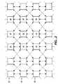
- FIG. 2shows an arrangement of storage elements (squares) in an array of memory cells in order to illustrate the capacitive coupling (dashed lines) between rows of them.
- a storage element 25 of a row 35for example, it is field coupled to storage elements in each of the adjacent rows 37 and 39 .
- the storage element 25is most closely coupled with the storage elements 27 and 31 , because of their proximity, but also have a lesser degree of coupling with storage elements 26 , 28 , 32 and 30 that are further away.
- the amount of coupling between two storage elementsdepends upon the distance between them, the dielectric constant of insulating material between them, whether there are any conductive surfaces between them, and the like.
- FIG. 2illustrates only field coupling between rows of storage elements, such coupling also exists between columns of storage elements. This is not being considered in the examples being described herein because, in these examples, data is programmed into memory cells in units of individual rows, the coupling between the rows has been found to be the cause of the apparent shift in programmed levels. For example, if data are programmed as distinct charge levels on the storage elements of the row 35 , a later change in the charge levels on either or both of the adjacent rows 37 and 39 will cause a shift in the apparent charge levels that are then read from the storage elements of the row 35 .
- the amount of such a shift in the apparent charge level read from a particular storage element of the row 35depends upon the degree of coupling with other storage elements whose charge was later changed in level and the amount of that change.
- the amounts of the shifts that resultare unknown unless the patterns of data programmed into each row are monitored and calculations of their effect made as part of each read operation.
- FIG. 3shows an example of the effect upon a first group of memory cells, such as a row of cells, of the later programming of a second group of memory cells, such as an adjacent row of cells.
- four distinct charge levelsare defined for each storage element, thereby to store two bits of data on each storage element. Since the level of charge stored on a storage element changes the threshold voltage (V T ) of its memory cell transistor, the threshold voltage is shown on the horizontal axis of the curves of FIG. 3 .
- the solid linesshow the distributions of the number of threshold voltages of all the cells in a page immediately after being programmed, before any change is made to the adjacent pages.
- the vertical axisis the number of cells at each threshold level, the curves having essentially a Gaussian distribution.
- a curve 45is the distribution of the cells in the erased state, which, in this example, is also designated as a programmed state of the bits 11 . When a block of cells is erased, the cells are reset to the 11 state.
- Each cell of a page being programmed to one of the other programmed states 47 , 49 or 51has electrons injected onto its storage element until its threshold reaches the state corresponding respectively to the data 01 , 00 or 01 being programmed into the cell.
- Suitable programming techniquesare described in other patents identified above in the Background. Briefly, cells of a page being programmed are programmed in parallel. Those being programmed into the 10 state are alternately pulsed with programming voltages and then verified by use of a verify threshold level V 10 . When it is determined that a cell has been programmed to a threshold level above V 10 , programming stops as to that cell but continues for other cells that have not yet reach their verify level. If being programmed to 00 , a verify level V 00 is used.
- a verify level V 01is used.
- the particular data bit pair assigned to each of the distributions 45 , 47 , 49 and 51may be different that shown in FIG. 3 , and may even be rotated during operation of the memory system in order to even out wear on the array.
- One technique used in the past to recover dataincludes reading the page again by simply moving the reading threshold levels R 10 , R 00 and/or R 01 within the margins to avoid the effect of the spreading. Since the spreading can come from both sides of each margin, however, this requires that the margins be maintained wider than is normally desired in order to prevent the distributions of adjacent states from overlapping. It is thus preferable to take some other steps to maintain wide margins between the programmed states.
- the programmed distributionsappear to spread in the manner shown in FIG. 3 when the data subsequently programmed into the adjacent page is random; that is, when the state stored in each storage element can be any of the four possible states.
- a storage element programmed to a level at the lower edge of the distribution 47for example, will be read to have the same level in the distribution 47 ′ if the charge level on adjacent storage elements does not change during the subsequent programming.
- a storage element initially programmed to a level at the upper edge of the distribution 47will, if the adjacent storage elements are subsequently programmed from an erased state 11 to the highest state 01 , be read to have a level that is increased by an amount ⁇ .
- FIGS. 4A , 4 B and 4 CAn example of a two pass technique for programming memory cells of the array of FIGS. 2 and 3 is given in FIGS. 4A , 4 B and 4 C.
- FIG. 4Afour state threshold distributions 61 , 62 , 63 and 64 resulting from a first programming pass of a group, such as a row, are shown.
- the distribution 61is for the erased state, which is also the programmed state 11 .
- the curve 62shows the distribution of the cells programmed to the 10 state by use of a verify threshold level V L10 during programming.
- the curve 63represents the distribution of the cells programmed to the 00 state with a V L00 verify level
- the curve 64the distribution of the cells programmed to the 01 state with a V L01 verify level.
- the programmingis accomplished in the typical manner described in the patents and patent applications referenced above, namely by alternately pulsing a chunk of cells being programmed in parallel and then reading (verifying) their states individually, with the programming of each cell being terminated when it is determined to exceed the verify threshold level of the state to which it is being programmed.
- the distributions 61 , 62 , 63 and 64individually have a width that is determined by the magnitude of increase in the level of each program pulse from the last.
- the distributions 61 , 62 , 63 and 64can be the same as the distributions 45 , 47 , 49 and 51 of FIG. 3 except that the cells represented by FIG. 4A are not yet fully programmed, while those represented by FIG. 3 are fully programmed.
- FIG. 4Bshows the broadened distributions of FIG. 4A that occur in the programmed cells when another group, such as a row, of physically adjacent cells are subsequently programmed with the same distributions.
- the distributions 61 , 62 , 63 and 64 of FIG. 4Aspread into respective distributions 71 , 72 , 73 and 74 upon the programming of the adjacent group of cells whose storage elements are field coupled with those whose thresholds are represented in FIGS. 4A and 4B .
- the spreadis by an amount ⁇ , as previously described with respect to FIG. 3 for respective distributions 45 ′, 47 ′, 49 ′ and 51 ′.
- the initially programmed group of cellsis again programmed with the same data as before but with higher verify levels.
- the verify levels V L— used in the initial programming illustrated in FIG. 4Aare less than the verify levels V H— used in the final re-programming of the same group of cells that is illustrated in FIG. 4 C.
- the differencecan be, in a specific implementation, the incremental threshold ⁇ , which is what is shown in FIG. 4 C. Since this second, final programming of a group of cells occurs after the programming to the first level (V L— ) of the adjacent group of cells, the effect of the adjacent cells through electric field coupling on the first group is automatically taken into account during the second programming step of FIG. 4 C.
- the cellsare programmed in the second pass with the field effect of the later programmed adjacent cells existing.
- the effect on the distributions of the first group of cells of the later second programming step of the adjacent group of cellsis very little since the thresholds are increased only a small amount in the second step. It will also be noticed that the distributions of FIG. 4C after the second programming step are narrowed to that of the first programming step of FIG. 4A , assuming that the same programming pulse incremental change is used in both the first and second programming passes of a group of cells.
- the increase of the charge level on the cells of the first group during the second programming passis preferably accomplished by re-programming the cells with the same data but with the higher verify threshold levels being used.
- This datacan remain in a buffer memory after the first programming pass until the second programming pass. But since this requires a larger buffer memory than usual, it is usually not desirable.
- the data programmed into a group of cells with the lower threshold levels V L —are read from that group after the adjacent group of cells is initially programmed. The read data is then re-programmed into the same cells but with the higher threshold levels V H— .
- Exemplary reading threshold levelsare also included in FIG. 4A for cells having been programmed by only the first pass, and in FIG. 4C for those having received both programming passes. In both cases, the read thresholds are positioned approximately mid-way in the margins between adjacent distributions. For cells programmed to the first level (FIG. 4 A), the read thresholds are R L10 , R L00 and R L01 positioned approximately mid-way between the adjacent distributions. After the second pass programming (FIG. 4 C), the read thresholds R H10 , R H00 and R H01 are used which correspond to those of FIG. 4A but are higher by some threshold amount, in this case ⁇ , in order to remain approximately mid-way between the repositioned distributions.
- some threshold amountin this case ⁇
- the programming and reading techniques being describedare beneficially applied to a memory system, such as flash EEPROM, that has its pages arranged in rows. That is, the techniques are used in a memory cell array where the unit of programming includes one or more rows of memory cells.
- the processcan be explained by reference to FIG. 2 .
- the storage elements of row 35are programmed with the first pass, followed by programming the storage elements of row 37 with the second pass if they were earlier programmed with the first pass.
- the row 39is then programmed with the first pass, followed by programming the row 35 with the second pass.
- the adjacent rows of memory cell storage elementsare programmed in this back-and-forth manner across an array until the unit of data being programmed has all been programmed. This is also the subject of FIG.
- the last row to be programmedis left programmed with the first pass, the second pass being deferred until a subsequent programming operation that starts with the next adjacent erased row of memory cells.
- An exception to thismay be when the last programmed row is also the last row in the block.
- the last row of a blockmay be programmed with one pass at the higher threshold levels V H— . Because blocks of cells are usually isolated from each other, there will be no other later programmed rows that have sufficient field coupling with the last row to affect the values read from the last row of the block.
- the programmed status of a rowis stored during programming as tracking bits (TB).
- This bitis preferably stored as part of the overhead data for the programmed page of user data.
- This tracking bitsare shown in FIG. 1 to be stored as part of the page overhead data in the same row as the user data.
- TBis set LOW to indicate that the programming has occurred with the lower set of verify thresholds.
- TBis rewritten to HIGH.
- FIG. 6shows the sequence of steps of programming a number of adjacent rows (such as illustrated in FIG. 5 ) in sequence by using the techniques described above. It will be assumed, for this example, that all pages of rows 0 , 1 and 2 are already programmed rows 0 and 1 with two passes but row 2 with only one pass.
- the immediately prior row 2is then addressed, as indicated at 95 . Data is then read from the prior row 2 with the low read levels (FIG.
- FIG. 7A process of reading data from rows programmed in the manner of FIG. 6 is illustrated in FIG. 7.
- User data 131 and overhead data 133 that pertain to the user dataare stored in a manner to be accessible to the user through the memory controller from the host device.
- the overhead data 133includes an ECC calculated from the user data, various flags and the like.
- Other overhead data 135such as a count of the number of times the block in which the page of FIG. 8 has been erased and re-programmed, voltages to be used for programming, reading and erasing, and the like, are hidden from access by the host but are used by the memory controller to operate the memory system.
- Also stored in the hidden regionare the TB bits and, typically, redundant cells 137 are included for substitution for any bits that fail in the user data region 131 .
- the usercannot access the TB bits from a host device; rather, the TB bits are written and read by the memory system controller.
Landscapes
- Engineering & Computer Science (AREA)
- Computer Hardware Design (AREA)
- Read Only Memory (AREA)
- Dram (AREA)
- Semiconductor Memories (AREA)
Abstract
Description
This application is a continuation of application Ser. No. 10/237,426, filed Sep. 6, 2002, now U.S. Pat. No. 6,781,877, which application is incorporated herein in its entirety by this reference.
This invention relates generally to the field of data memories, and, more specifically, to memories of the type that store data as levels of electronic charge, including, but not limited to, flash electrically erasable and programmable read-only-memories (flash EEPROMs) utilizing either conductive floating gates or dielectric material as charge storage elements.
It is common in current commercial products for each storage element of a flash EEPROM array to store a single bit of data by operating in a binary mode, where two ranges of threshold levels of the storage element transistors are defined as storage levels. The threshold levels of transistors correspond to ranges of charge levels stored on their storage elements. In addition to shrinking the size of the memory arrays, the trend is to further increase the density of data storage of such memory arrays by storing more than one bit of data in each storage element transistor. This is accomplished by defining more than two threshold levels as storage states for each storage element transistor, four such states (2 bits of data per storage element) now being included in commercial products. More storage states, such as 16 states (4 data bits) per storage element, are contemplated. Each storage element memory transistor has a certain total range (window) of threshold voltages in which it may practically be operated, and that range is divided into the number of states defined for it plus margins between the states to allow for them to be clearly differentiated from one another.
As the number of states stored in each memory cell increases, the tolerance of any shifts in the programmed charge level on the storage elements decreases. Since the ranges of charge designated for each storage state must necessarily be made narrower and placed closer together as the number of states stored on each memory cell storage element increases, the programming must be performed with an increased degree of precision and the extent of any post-programming shifts in the stored charge levels that can be tolerated, either actual or apparent shifts, is reduced. Actual disturbs to the charge stored in one cell can be created when programming and reading that cell, and when reading, programming and erasing other cells that have some degree of electrical coupling with that cell, such as those in the same column or row, and those sharing a line or node.
Apparent shifts in the stored charge levels occur because of field coupling between storage elements. The degree of this coupling is necessarily increasing as the spaces between memory cell storage elements are being decreased, which is occurring as the result of improvements of integrated circuit manufacturing techniques. The problem occurs most pronouncedly between two groups of adjacent cells that have been programmed at different times. One group of cells is programmed to add a level of charge to their storage elements that corresponds to one set of data. After the second group of cells is programmed with a second set of data, the charge levels read from the storage elements of the first group of cells often appear to be different than programmed because of the effect of the charge on the second group of storage elements being capacitively coupled with the first. This is known as the Yupin effect, and is described in U.S. Pat. No. 5,867,429, which patent is incorporated herein in their entirety by this reference. This patent describes either physically isolating the two groups of storage elements from each other, or taking into account the effect of the charge on the second group of storage elements when reading that of the first group.
According to an application of one aspect of the present invention, in order to overcome the effects on each other of adjacent programmed rows of memory cells, adjacent rows are programmed in two steps. In a first step, a first row of memory cells is programmed with data to a first, intermediate set of threshold levels. After a second adjacent row of memory cells is similarly programmed, the threshold levels of the first row of memory cells are increased to a second, final set of threshold levels. Since the final programming of the first row occurs under the influence of the second row's initial programming, data read from the first row is not adversely affected by the levels initially programmed into the second row. After a third row adjacent the second row is programmed to the first set of threshold levels, the threshold levels of the second row are increased to the final set. The process is continued for the programming of any additional rows of memory cells having field coupling between adjacent rows.
According to an application of another aspect of the present invention, an identification of the set of levels at which a group, such as a row, of cells has been programmed is stored in a manner to be read along with the programmed group of cells. A group of memory cells is initially read with applied read voltages chosen for optimally reading cells programmed with the most common one of the sets of levels. If the initially read identification shows that the cells were programmed with the other set of levels, however, the group of cells is re-read with applied read voltages corresponding to the other set of levels.
The present invention can be implemented in various types of flash EEPROM cell arrays. A NOR array of one design has its memory cells connected between adjacent bit (column) lines and control gates connected to word (row) lines. The individual cells contain either one storage element transistor, with or without a select transistor formed in series with it, or two storage element transistors separated by a single select transistor. Examples of such arrays and their use in storage systems are given in the following U.S. patents and pending applications of SanDisk Corporation that are incorporated herein in their entirety by this reference: U.S. Pat. Nos. 5,095,344, 5,172,338, 5,602,987, 5,663,901, 5,430,859, 5,657,332, 5,712,180, 5,890,192, 6,091,633, 6,103,573, 6,151,248, 6,426,893, 6,512,263, 6,762,092 and application Ser. No. 09/925,134, filed Aug. 8, 2001.
A NAND array of one design has a number of memory cells, such as 8, 16 or even 32, connected in a series string between a bit line and a reference potential through select transistors at either end. Word lines are connected with control gates of cells across different series strings. Relevant examples of such arrays and their operation are given in the following U.S. patents and patent application that are incorporated herein in their entirety by this reference: U.S. Pat. Nos. 5,570,315, 5,774,397 and 6,046,935, and application Ser. No. 09/893,277, filed 6,522,580. Briefly, two bits of data from different logical pages of incoming data are programmed into one of four states of the individual cells in two steps, first programming a cell into one state according to one bit of data and then, if the data makes it necessary, re-programming that cell into another one of its states according to the second bit of incoming data.
The above-referenced patents and patent applications describe flash EEPROM systems that use conductive floating gates as memory cell storage elements. Alternatively, flash EEPROM systems with memory cells employing charge trapping dielectric material in place of floating gates are operated in substantially the same way. Examples of this are included in patent application Ser. No. 10/002,696, filed Oct. 31, 2001, by Harari et al., entitled “Multi-State Non-Volatile Integrated Circuit Memory Systems that Employ Dielectric Storage Elements,” published as US 2003/0082871 A1 on May 1, 2003 which application is incorporated herein by this reference. Field coupling between dielectric storage elements of adjacent memory cells can also affect the accuracy of the data read from such memory systems.
Additional aspects, features and advantages of the present invention can be had from the following detailed description of exemplary embodiments thereof, which description should be read along with reference to the accompanying drawings.
In order to explain the present invention and example implementations, a general diagram of the interrelationship of major components of an example mass memory system is shown inFIG. 1. A primary component of this system is amemory 11, such as an array of memory cells formed on a semiconductor substrate, wherein one or more bits of data are stored in the individual memory cells by storing one of two or more levels of charge on individual storage elements of the memory cells. A non-volatile flash EEPROM is a common type of memory for such systems, and is used in this example.
A second primary component of the memory system ofFIG. 1 is acontroller 13. Thecontroller 13 communicates over abus 15 to a host computer or other system that is using the memory system to store data. Thecontroller 13 also controls operation of thememory cell array 11 to write data provided by the host, read data requested by the host and perform various housekeeping functions in operating the memory. Thecontroller 13 normally includes a general-purpose microprocessor, with associated non-5 volatile software memory, various logic circuits, and the like. One or more state machines and other controlling circuits may be included as part of the array for controlling the performance of specific routines, in which case the role of the system controller is reduced.
Thememory cell array 11 is addressed by thecontroller 13 throughaddress decoders 17. Thedecoders 17 apply the correct voltages to gate and bit lines of thearray 11 in order to program data to, read data from, or erase a group of memory cells being addressed by thecontroller 13.Additional circuits 19 include programming drivers that control voltages applied to elements of the array that depend upon the data being programmed into an addressed group of cells. Thecircuits 19 also include sense amplifiers and other circuits necessary to read data from an addressed group of memory cells. Various specific forms of thecircuits buffer memory 21 within thecontroller 13. Thecontroller 13 also usually contains various registers for temporarily storing command and status data, and the like.
Thearray 11 is divided into a large number of BLOCKS0-N of memory cells. As is common for flash EEPROM systems, the block is the unit of erase. That is, each block contains the minimum number of memory cells that are erased together. Each block is typically divided into a number of pages, as also illustrated inFIG. 1. A page is a unit of programming but the individual pages may be divided into segments. A segment may contain the fewest number of cells that are written at one time as a basic programming operation, storing as little as one byte of data. One or more pages of data are typically stored in one row of memory cells. One sector of data is usually stored within each page, although multiple sectors may be included. As shown inFIG. 1 , a sector includes user data and overhead data. Overhead data typically includes an ECC that has been calculated from the user data of the sector. Aportion 23 of thecontroller 13 calculates the ECC when data is being programmed into thearray 11, and also checks it when data is being read from thearray 11. Alternatively, the ECCs and/or other overhead data are stored in different pages, or even different blocks, than the user data to which they pertain. The overhead data include one or more TB bits (Tracking Bit(s)) that designate the threshold verify level with which the page of data has been programmed. Uses of the TB field are described hereinafter.
A sector of user data is typically 512 bytes, corresponding to the size of a sector in magnetic disk drives. Overhead data is typically an additional 16-20 bytes. One sector of data is most commonly included in each page but two or more sectors may instead form a page. A large number of pages form a block, anywhere from 8 pages, for example, up to 32, 64 or more pages. The number of blocks is chosen to provide a desired data storage capacity for the memory system. Thearray 11 is typically divided into a few sub-arrays (not shown), each of which contains a proportion of the blocks, which operate somewhat independently of each other in order to increase the degree of parallelism in the execution of various memory operations. An example of the use of multiple sub-arrays is described in U.S. Pat. No. 5,890,192, which patent is incorporated herein by this reference.
AlthoughFIG. 2 illustrates only field coupling between rows of storage elements, such coupling also exists between columns of storage elements. This is not being considered in the examples being described herein because, in these examples, data is programmed into memory cells in units of individual rows, the coupling between the rows has been found to be the cause of the apparent shift in programmed levels. For example, if data are programmed as distinct charge levels on the storage elements of therow 35, a later change in the charge levels on either or both of theadjacent rows row 35. The amount of such a shift in the apparent charge level read from a particular storage element of therow 35 depends upon the degree of coupling with other storage elements whose charge was later changed in level and the amount of that change. When the later change is caused by programming data into the adjacent row, the amounts of the shifts that result are unknown unless the patterns of data programmed into each row are monitored and calculations of their effect made as part of each read operation.
Each cell of a page being programmed to one of the otherprogrammed states distributions FIG. 3 , and may even be rotated during operation of the memory system in order to even out wear on the array.
It is desired to maintain a sufficient margin between thestates FIG. 3 as R10(VT=0), R00and R01. Of course, in order to be able to fully use an available threshold window, as many different states are included as is practical, four states being shown. Another example is sixteen states. A larger number of states can result from the width of the distributions being narrowed by programming with smaller voltage increments in successive pulses but this then takes more time to perform the programming. It is therefore desirable, either alone or along with narrowing the programmed cell distributions, to take steps to reduce the need for such large margins between states. Rather large margins are usually maintained in order to allow for the programmed cell distributions to shift or spread as a result of repetitive operating cycles that occur after their programming, as experience has shown to occur. It is highly desirable to reduce such shifting and spreading in order to be able to reduce the amount width of the margins between states.
The spreading of the distributions that occurs as the result of subsequently programming an adjacent row of cells is shown in dashed lines in FIG.3. Even when significant margins are maintained during the initial programming of a row of cells, these margins can be significantly narrowed when the distributions spread as a result of later programming an adjacent row of cells. If just a few of the cells spread from below to above one of the reading thresholds R10, R00and/or R01, there can be enough erroneous readings to overwhelm an ECC. In such a case, the data cannot be read with those thresholds, so are normally designated as invalid unless some extraordinary action is taken. One technique used in the past to recover data includes reading the page again by simply moving the reading threshold levels R10, R00and/or R01within the margins to avoid the effect of the spreading. Since the spreading can come from both sides of each margin, however, this requires that the margins be maintained wider than is normally desired in order to prevent the distributions of adjacent states from overlapping. It is thus preferable to take some other steps to maintain wide margins between the programmed states.
The programmed distributions appear to spread in the manner shown inFIG. 3 when the data subsequently programmed into the adjacent page is random; that is, when the state stored in each storage element can be any of the four possible states. A storage element programmed to a level at the lower edge of thedistribution 47, for example, will be read to have the same level in thedistribution 47′ if the charge level on adjacent storage elements does not change during the subsequent programming. On the other hand, a storage element initially programmed to a level at the upper edge of thedistribution 47 will, if the adjacent storage elements are subsequently programmed from an erasedstate 11 to the highest state01, be read to have a level that is increased by an amount Δ. The higher charge levels on the adjacent storage elements are coupled with the previously programmed storage element whose level is being read. Other combinations of initial and later programming of adjacent cells of thedistribution 47 fall between these two extremes, thereby resulting in theapparent distribution 47′. The lower end of theapparent distribution 47′ remains at the same level but its spread is increased by Δ.
An example of a two pass technique for programming memory cells of the array ofFIGS. 2 and 3 is given inFIGS. 4A ,4B and4C. InFIG. 4A , fourstate threshold distributions distribution 61 is for the erased state, which is also the programmedstate 11. Thecurve 62 shows the distribution of the cells programmed to the 10 state by use of a verify threshold level VL10during programming. Similarly, thecurve 63 represents the distribution of the cells programmed to the 00 state with a VL00verify level, and thecurve 64 the distribution of the cells programmed to the 01 state with a VL01verify level. The programming is accomplished in the typical manner described in the patents and patent applications referenced above, namely by alternately pulsing a chunk of cells being programmed in parallel and then reading (verifying) their states individually, with the programming of each cell being terminated when it is determined to exceed the verify threshold level of the state to which it is being programmed. Thedistributions distributions distributions FIG. 3 except that the cells represented byFIG. 4A are not yet fully programmed, while those represented byFIG. 3 are fully programmed.
After the programming of the adjacent group of cells occurs, which has resulted in the spreading shown inFIG. 4B , the initially programmed group of cells is again programmed with the same data as before but with higher verify levels. The verify levels VL— used in the initial programming illustrated inFIG. 4A are less than the verify levels VH— used in the final re-programming of the same group of cells that is illustrated in FIG.4C. The difference can be, in a specific implementation, the incremental threshold Δ, which is what is shown in FIG.4C. Since this second, final programming of a group of cells occurs after the programming to the first level (VL—) of the adjacent group of cells, the effect of the adjacent cells through electric field coupling on the first group is automatically taken into account during the second programming step of FIG.4C. The cells are programmed in the second pass with the field effect of the later programmed adjacent cells existing. The effect on the distributions of the first group of cells of the later second programming step of the adjacent group of cells is very little since the thresholds are increased only a small amount in the second step. It will also be noticed that the distributions ofFIG. 4C after the second programming step are narrowed to that of the first programming step ofFIG. 4A , assuming that the same programming pulse incremental change is used in both the first and second programming passes of a group of cells.
Although it can be done by other techniques, the increase of the charge level on the cells of the first group during the second programming pass is preferably accomplished by re-programming the cells with the same data but with the higher verify threshold levels being used. This data can remain in a buffer memory after the first programming pass until the second programming pass. But since this requires a larger buffer memory than usual, it is usually not desirable. Preferably, the data programmed into a group of cells with the lower threshold levels VL— are read from that group after the adjacent group of cells is initially programmed. The read data is then re-programmed into the same cells but with the higher threshold levels VH—.
Exemplary reading threshold levels are also included inFIG. 4A for cells having been programmed by only the first pass, and inFIG. 4C for those having received both programming passes. In both cases, the read thresholds are positioned approximately mid-way in the margins between adjacent distributions. For cells programmed to the first level (FIG.4A), the read thresholds are RL10, RL00and RL01positioned approximately mid-way between the adjacent distributions. After the second pass programming (FIG.4C), the read thresholds RH10, RH00and RH01are used which correspond to those ofFIG. 4A but are higher by some threshold amount, in this case Δ, in order to remain approximately mid-way between the repositioned distributions.
The programming and reading techniques being described are beneficially applied to a memory system, such as flash EEPROM, that has its pages arranged in rows. That is, the techniques are used in a memory cell array where the unit of programming includes one or more rows of memory cells. For example, the process can be explained by reference to FIG.2. The storage elements ofrow 35 are programmed with the first pass, followed by programming the storage elements ofrow 37 with the second pass if they were earlier programmed with the first pass. Therow 39 is then programmed with the first pass, followed by programming therow 35 with the second pass. The adjacent rows of memory cell storage elements are programmed in this back-and-forth manner across an array until the unit of data being programmed has all been programmed. This is also the subject ofFIG. 5 , where the progress of programming rows0-7 is illustrated. The last row to be programmed is left programmed with the first pass, the second pass being deferred until a subsequent programming operation that starts with the next adjacent erased row of memory cells. An exception to this may be when the last programmed row is also the last row in the block. The last row of a block may be programmed with one pass at the higher threshold levels VH—. Because blocks of cells are usually isolated from each other, there will be no other later programmed rows that have sufficient field coupling with the last row to affect the values read from the last row of the block.
Since the optimum read voltages for a row depend upon whether the row has been programmed with only one pass (FIG. 4A ) or two passes (FIG.4C), the programmed status of a row is stored during programming as tracking bits (TB). This bit is preferably stored as part of the overhead data for the programmed page of user data. This tracking bits are shown inFIG. 1 to be stored as part of the page overhead data in the same row as the user data. As part of the first programming pass, TB is set LOW to indicate that the programming has occurred with the lower set of verify thresholds. As part of the second programming pass, TB is rewritten to HIGH. In the four state example being described, TB most conveniently uses two bits: For the first pass, TB=11 (LOW), the erased state of one cell, and after the second pass, TB=10 (HIGH), a higher programmed state of that cell. This allows the TB of a page to be easily updated as part of the second programming pass by additional programming of it.
Reading normally occurs with the higher read voltages (FIG. 4C ) since most all rows are programmed with two passes. But as part of this initial read operation, the TB is also read. Its value is determined early in the process of reading the page. If TB=LOW, then the page is re-read with the lower set of read voltages (FIG.4A). Although this requires two reads of some rows, memory performance is not significantly affected because there will normally be a very small proportion of the rows in a memory array that remain programmed with the lower levels at any one time. Even though a row programmed with the lower verify levels is being read with the higher read levels, there should be no error in reading its tracking bits when the erasedstate 11 is used to indicate TB=LOW.
The flow chart ofFIG. 6 shows the sequence of steps of programming a number of adjacent rows (such as illustrated inFIG. 5 ) in sequence by using the techniques described above. It will be assumed, for this example, that all pages ofrows rows row 2 with only one pass. A first step in programmingsubsequent rows 3+with data is to addressrow 3, as indicated at91 of FIG.6. All pages ofrow 3 are then programmed by a first pass (FIG. 4A ) with TB=LOW, as indicated at93. The immediatelyprior row 2 is then addressed, as indicated at95. Data is then read from theprior row 2 with the low read levels (FIG.4A), as indicated at97, including its TB, as indicated at99. If TB=LOW, which it does in this example, then the read TB is updated to TB=HIGH, at10. The read data is then re-programmed into theprior row 2, along with its TB=HIGH, as indicated at103. This completes one cycle of data programming. But since most data programming operations involve programming more pages than are included in one row, it is determined at105 whether additional rows are to be programmed. If so, the process is repeated by programming the next erasedrow 4 with a first pass, followed by increasing the charge levels ofrow 5 by re-programming its data. This cycle continues along the rows ofFIG. 5 , where the memory cell storage elements of adjacent rows are capacitively coupled with each other to a significant level.
A process of reading data from rows programmed in the manner ofFIG. 6 is illustrated inFIG. 7. A first row to be read is addressed, as indicated at107. That row is then read with the higher read voltages (FIG.4C), as indicated at109. Since this read also includes reading the tracking bit, it is determined, at111, whether TB=LOW or TB=HIGH. If TB=LOW, the row is re-read with the lower read levels (FIG.4A), as indicated at113, followed by temporarily storing the read data, at115. This completes the read for one row. But since most reading operations are of many rows in sequence, aninquiry 117 determines whether more rows are to be read. If so, the next row in order is read, as indicated at119, and the process returns to109.
With reference toFIG. 8 , one example of the data structure of a page of memory cells is described.User data 131 andoverhead data 133 that pertain to the user data are stored in a manner to be accessible to the user through the memory controller from the host device. Theoverhead data 133 includes an ECC calculated from the user data, various flags and the like. Otheroverhead data 135, such as a count of the number of times the block in which the page ofFIG. 8 has been erased and re-programmed, voltages to be used for programming, reading and erasing, and the like, are hidden from access by the host but are used by the memory controller to operate the memory system. Also stored in the hidden region are the TB bits and, typically,redundant cells 137 are included for substitution for any bits that fail in theuser data region 131. Thus, the user cannot access the TB bits from a host device; rather, the TB bits are written and read by the memory system controller.
Although the present invention has been described with respect to exemplary embodiments, it will be understood that the invention is entitled to protection within the full scope of the appended claims.
Claims (6)
1. A memory system, comprising:
an array of rows and columns of re-programmable non-volatile memory cells that include charge storage elements that individually store levels of charge indicative of data stored therein, wherein a degree of field coupling exists between the charge storage elements of memory cells of adjacent rows, and
programming circuits that successively program memory cells of individual rows of a unit of rows by causing the memory cells of a first row to be programmed and verified to have intermediate data storage charge levels along with an indication that the intermediate levels have been used, by thereafter causing the memory cells of a second row adjacent the first row to be programmed and verified to have intermediate data storage charge levels along with an indication that the intermediate levels have been used, by thereafter causing the memory cells of the first row to be further programmed and verified to have final data storage charge levels along with an indication that the final levels have been used, by thereafter causing the memory cells of a third row adjacent the second row to be programmed and verified to have intermediate data storage charge levels along with an indication that the intermediate levels have been used, by thereafter causing the memory cells of the second row to be further programmed and verified to have final data storage charge levels along with an indication that the final levels have been used, and that repeats this process row-by-row until all the rows of the unit have been programmed to the final data storage charge levels.
2. The memory system ofclaim 1 , wherein the programming circuits further cause the final charge storage levels to which individual charge storage elements of the memory cells are programmed to be more than two charge storage levels.
3. The memory system ofclaim 1 , wherein the array of memory cells utilize a NAND architecture.
4. The memory system ofclaim 1 , wherein the unit of rows is within a block of memory cells of the array, wherein the memory cells within the block are erasable together prior to programming them.
5. The memory system ofclaim 1 , wherein the unit of rows has a capacity to store a page of data.
6. The memory system ofclaim 1 , additionally comprising reading circuits that read the intermediate storage charge levels of a given row as the source of data for the programming circuits to thereafter cause the memory cells of the given row to be programmed and verified to have final data storage charge levels.
Priority Applications (2)
| Application Number | Priority Date | Filing Date | Title |
|---|---|---|---|
| US10/923,320US6870768B2 (en) | 2002-09-06 | 2004-08-20 | Techniques for reducing effects of coupling between storage elements of adjacent rows of memory cells |
| US11/055,776US7046548B2 (en) | 2002-09-06 | 2005-02-09 | Techniques for reducing effects of coupling between storage elements of adjacent rows of memory cells |
Applications Claiming Priority (2)
| Application Number | Priority Date | Filing Date | Title |
|---|---|---|---|
| US10/237,426US6781877B2 (en) | 2002-09-06 | 2002-09-06 | Techniques for reducing effects of coupling between storage elements of adjacent rows of memory cells |
| US10/923,320US6870768B2 (en) | 2002-09-06 | 2004-08-20 | Techniques for reducing effects of coupling between storage elements of adjacent rows of memory cells |
Related Parent Applications (1)
| Application Number | Title | Priority Date | Filing Date |
|---|---|---|---|
| US10/237,426ContinuationUS6781877B2 (en) | 2002-09-06 | 2002-09-06 | Techniques for reducing effects of coupling between storage elements of adjacent rows of memory cells |
Related Child Applications (1)
| Application Number | Title | Priority Date | Filing Date |
|---|---|---|---|
| US11/055,776ContinuationUS7046548B2 (en) | 2002-09-06 | 2005-02-09 | Techniques for reducing effects of coupling between storage elements of adjacent rows of memory cells |
Publications (2)
| Publication Number | Publication Date |
|---|---|
| US20050018482A1 US20050018482A1 (en) | 2005-01-27 |
| US6870768B2true US6870768B2 (en) | 2005-03-22 |
Family
ID=31977713
Family Applications (3)
| Application Number | Title | Priority Date | Filing Date |
|---|---|---|---|
| US10/237,426Expired - LifetimeUS6781877B2 (en) | 2002-09-06 | 2002-09-06 | Techniques for reducing effects of coupling between storage elements of adjacent rows of memory cells |
| US10/923,320Expired - LifetimeUS6870768B2 (en) | 2002-09-06 | 2004-08-20 | Techniques for reducing effects of coupling between storage elements of adjacent rows of memory cells |
| US11/055,776Expired - LifetimeUS7046548B2 (en) | 2002-09-06 | 2005-02-09 | Techniques for reducing effects of coupling between storage elements of adjacent rows of memory cells |
Family Applications Before (1)
| Application Number | Title | Priority Date | Filing Date |
|---|---|---|---|
| US10/237,426Expired - LifetimeUS6781877B2 (en) | 2002-09-06 | 2002-09-06 | Techniques for reducing effects of coupling between storage elements of adjacent rows of memory cells |
Family Applications After (1)
| Application Number | Title | Priority Date | Filing Date |
|---|---|---|---|
| US11/055,776Expired - LifetimeUS7046548B2 (en) | 2002-09-06 | 2005-02-09 | Techniques for reducing effects of coupling between storage elements of adjacent rows of memory cells |
Country Status (10)
| Country | Link |
|---|---|
| US (3) | US6781877B2 (en) |
| EP (1) | EP1535285B1 (en) |
| JP (1) | JP4391941B2 (en) |
| KR (1) | KR100986680B1 (en) |
| CN (1) | CN100578667C (en) |
| AT (1) | ATE321339T1 (en) |
| AU (1) | AU2003262675A1 (en) |
| DE (1) | DE60304220T2 (en) |
| ES (1) | ES2262014T3 (en) |
| WO (1) | WO2004023489A1 (en) |
Cited By (81)
| Publication number | Priority date | Publication date | Assignee | Title |
|---|---|---|---|---|
| US20050146931A1 (en)* | 2002-09-06 | 2005-07-07 | Raul-Adrian Cernea | Techniques for reducing effects of coupling between storage elements of adjacent rows of memory cells |
| US20060221714A1 (en)* | 2005-04-05 | 2006-10-05 | Yan Li | Read operation for non-volatile storage that includes compensation for coupling |
| US20060221692A1 (en)* | 2005-04-05 | 2006-10-05 | Jian Chen | Compensating for coupling during read operations on non-volatile memory |
| US20060221683A1 (en)* | 2005-04-05 | 2006-10-05 | Jian Chen | Compensating for coupling in non-volatile storage |
| US20070153583A1 (en)* | 2005-12-29 | 2007-07-05 | Guterman Daniel C | Alternate row-based reading and writing for non-volatile memory |
| US20070153577A1 (en)* | 2005-12-29 | 2007-07-05 | Guterman Daniel C | Systems for alternate row-based reading and writing for non-volatile memory |
| US20070206421A1 (en)* | 2006-03-03 | 2007-09-06 | Nima Mokhlesi | Read operation for non-volatile storage with compensation for coupling |
| US20070206426A1 (en)* | 2006-03-03 | 2007-09-06 | Nima Mokhlesi | System for performing read operation on non-volatile storage with compensation for coupling |
| US20070279995A1 (en)* | 2006-06-02 | 2007-12-06 | Nima Mokhlesi | System for performing data pattern sensitivity compensation using different voltage |
| US20070279985A1 (en)* | 2006-06-01 | 2007-12-06 | Gerrit Jan Hemink | System for verifying non-volatile storage using different voltages |
| US20070279993A1 (en)* | 2006-06-01 | 2007-12-06 | Gerrit Jan Hemink | Verify operation for non-volatile storage using different voltages |
| US20070279994A1 (en)* | 2006-06-02 | 2007-12-06 | Nima Mokhlesi | Data pattern sensitivity compensation using different voltage |
| US20070291556A1 (en)* | 2006-06-19 | 2007-12-20 | Teruhiko Kamei | Programming Differently Sized Margins and Sensing with Compensations at Select States for Improved Read Operations in Non-Volatile Memory |
| US20070291546A1 (en)* | 2006-06-19 | 2007-12-20 | Teruhiko Kamei | Systems for Programming Differently Sized Margins and Sensing with Compensations at Select States for Improved Read Operations in Non-Volatile Memory |
| US20080008000A1 (en)* | 2005-11-10 | 2008-01-10 | Jian Chen | Reverse coupling effect with timing information |
| US20080019186A1 (en)* | 2006-07-20 | 2008-01-24 | Yan Li | System that compensates for coupling during programming |
| US20080019174A1 (en)* | 2006-07-20 | 2008-01-24 | Yan Li | Method for configuring compensation |
| US20080019173A1 (en)* | 2006-07-20 | 2008-01-24 | Yan Li | System for configuring compensation |
| US20080019193A1 (en)* | 2006-07-20 | 2008-01-24 | Yan Li | Compensating for coupling based on sensing a neighbor using coupling |
| US20080019185A1 (en)* | 2006-07-20 | 2008-01-24 | Yan Li | Compensating for coupling during programming |
| US20080019175A1 (en)* | 2006-07-20 | 2008-01-24 | Yan Li | System that compensates for coupling based on sensing a neighbor using coupling |
| US20080065813A1 (en)* | 2006-09-08 | 2008-03-13 | Yan Li | Methods in a pseudo random and command driven bit compensation for the cycling effects in flash memory |
| US20080065812A1 (en)* | 2006-09-08 | 2008-03-13 | Yan Li | Pseudo random and command driven bit compensation for the cycling effects in flash memory |
| US20080084755A1 (en)* | 2006-09-29 | 2008-04-10 | Nima Mokhlesi | Systems for reverse reading in non-volatile memory with compensation for coupling |
| US20080084754A1 (en)* | 2006-09-29 | 2008-04-10 | Nima Mokhlesi | Reverse reading in non-volatile memory with compensation for coupling |
| US20080158974A1 (en)* | 2006-12-29 | 2008-07-03 | Nima Mokhlesi | Apparatus with alternating read mode |
| US20080158983A1 (en)* | 2006-12-29 | 2008-07-03 | Nima Mokhlesi | Non-volatile storage system with resistance sensing and compensation |
| US20080158949A1 (en)* | 2006-12-28 | 2008-07-03 | Man Lung Mui | Systems for complete word line look ahead with efficient data latch assignment in non-volatile memory read operations |
| US20080158967A1 (en)* | 2006-12-29 | 2008-07-03 | Nima Mokhlesi | Resistance sensing and compensation for non-volatile storage |
| US20080158985A1 (en)* | 2006-12-29 | 2008-07-03 | Nima Mokhlesi | Systems for margined neighbor reading for non-volatile memory read operations including coupling compensation |
| US20080158984A1 (en)* | 2006-12-29 | 2008-07-03 | Nima Mokhlesi | Margined neighbor reading for non-volatile memory read operations including coupling compensation |
| US20080158946A1 (en)* | 2006-12-29 | 2008-07-03 | Nima Mokhlesi | Alternating read mode |
| US20080158973A1 (en)* | 2006-12-28 | 2008-07-03 | Man Lung Mui | Complete word line look ahead with efficient data latch assignment in non-volatile memory read operations |
| US20080273388A1 (en)* | 2007-03-21 | 2008-11-06 | Henry Chin | Adjusting resistance of non-volatile memory using dummy memory cells |
| US20090040839A1 (en)* | 2007-08-06 | 2009-02-12 | Spansion Llc | Reading multi-cell memory devices utilizing complementary bit information |
| US20090067244A1 (en)* | 2007-09-07 | 2009-03-12 | Yan Li | Nonvolatile memory and method for on-chip pseudo-randomization of data within a page and between pages |
| US20090310413A1 (en)* | 2008-06-16 | 2009-12-17 | Sandisk Il Ltd. | Reverse order page writing in flash memories |
| US20100097861A1 (en)* | 2008-10-16 | 2010-04-22 | Deepanshu Dutta | Multi-Pass Programming For Memory Using Word Line Coupling |
| US20100149868A1 (en)* | 2008-12-12 | 2010-06-17 | Samsung Electronics Co., Ltd. | Access method of non-volatile memory device |
| US20100309720A1 (en)* | 2009-06-05 | 2010-12-09 | Bo Liu | Structure and Method for Shuffling Data Within Non-Volatile Memory Devices |
| US20100309719A1 (en)* | 2009-06-05 | 2010-12-09 | Yan Li | Folding Data Stored in Binary Format Into Multi-State Format Within Non-Volatile Memory Devices |
| US20110002169A1 (en)* | 2009-07-06 | 2011-01-06 | Yan Li | Bad Column Management with Bit Information in Non-Volatile Memory Systems |
| US20110044102A1 (en)* | 2009-08-19 | 2011-02-24 | Yingda Dong | Selective memory cell program and erase |
| US20110055670A1 (en)* | 2008-03-12 | 2011-03-03 | Macronix International Co., Ltd. | Programming Method and Memory Device Using the Same |
| US20110153912A1 (en)* | 2009-12-18 | 2011-06-23 | Sergey Anatolievich Gorobets | Maintaining Updates of Multi-Level Non-Volatile Memory in Binary Non-Volatile Memory |
| WO2011075594A1 (en) | 2009-12-18 | 2011-06-23 | Sandisk Corporation | Non-volatile memory with multi-gear control using on-chip folding of data |
| WO2011075597A1 (en) | 2009-12-18 | 2011-06-23 | Sandisk Corporation | Data transfer flows for on-chip folding |
| US20110205782A1 (en)* | 2010-02-23 | 2011-08-25 | Xiying Chen Costa | Step soft program for reversible resistivity-switching elements |
| WO2011162973A1 (en) | 2010-06-23 | 2011-12-29 | Sandisk Technologies Inc. | Use of guard bands and phased maintenance operations to avoid exceeding maximum latency requirements in non-volatile memory systems |
| WO2012087569A1 (en) | 2010-12-21 | 2012-06-28 | Sandisk Technologies Inc. | Alternate page by page programming scheme |
| US8310870B2 (en) | 2010-08-03 | 2012-11-13 | Sandisk Technologies Inc. | Natural threshold voltage distribution compaction in non-volatile memory |
| US8385102B2 (en) | 2010-05-11 | 2013-02-26 | Sandisk 3D Llc | Alternating bipolar forming voltage for resistivity-switching elements |
| TWI391934B (en)* | 2006-12-28 | 2013-04-01 | Sandisk Technologies Inc | Non-volatile memory system and method of reading non-volatile storage |
| TWI397075B (en)* | 2006-12-29 | 2013-05-21 | Sandisk Technologies Inc | Alternating read mode |
| US8543757B2 (en) | 2010-06-23 | 2013-09-24 | Sandisk Technologies Inc. | Techniques of maintaining logical to physical mapping information in non-volatile memory systems |
| US8681548B2 (en) | 2012-05-03 | 2014-03-25 | Sandisk Technologies Inc. | Column redundancy circuitry for non-volatile memory |
| US8725935B2 (en) | 2009-12-18 | 2014-05-13 | Sandisk Technologies Inc. | Balanced performance for on-chip folding of non-volatile memories |
| TWI451422B (en)* | 2006-06-19 | 2014-09-01 | Sandisk Technologies Inc | Method and systems for programming differently sized margins and sensing with compensations at select states for improved read operations in non-volatile memory |
| US8843693B2 (en) | 2011-05-17 | 2014-09-23 | SanDisk Technologies, Inc. | Non-volatile memory and method with improved data scrambling |
| US8842473B2 (en) | 2012-03-15 | 2014-09-23 | Sandisk Technologies Inc. | Techniques for accessing column selecting shift register with skipped entries in non-volatile memories |
| US8897080B2 (en) | 2012-09-28 | 2014-11-25 | Sandisk Technologies Inc. | Variable rate serial to parallel shift register |
| US9047970B2 (en) | 2013-10-28 | 2015-06-02 | Sandisk Technologies Inc. | Word line coupling for deep program-verify, erase-verify and read |
| US9076506B2 (en) | 2012-09-28 | 2015-07-07 | Sandisk Technologies Inc. | Variable rate parallel to serial shift register |
| US9087595B2 (en) | 2012-04-20 | 2015-07-21 | Aplus Flash Technology, Inc. | Shielding 2-cycle half-page read and program schemes for advanced NAND flash design |
| WO2015142513A1 (en) | 2014-03-17 | 2015-09-24 | Sandisk Technologies Inc. | Detection of read disturbances on non-volatile memories through counting of read accesses within divisions of the memory |
| US9171627B2 (en) | 2012-04-11 | 2015-10-27 | Aplus Flash Technology, Inc. | Non-boosting program inhibit scheme in NAND design |
| US9183940B2 (en) | 2013-05-21 | 2015-11-10 | Aplus Flash Technology, Inc. | Low disturbance, power-consumption, and latency in NAND read and program-verify operations |
| US9224502B1 (en) | 2015-01-14 | 2015-12-29 | Sandisk Technologies Inc. | Techniques for detection and treating memory hole to local interconnect marginality defects |
| US9230677B2 (en) | 2013-07-25 | 2016-01-05 | Aplus Flash Technology, Inc | NAND array hiarchical BL structures for multiple-WL and all-BL simultaneous erase, erase-verify, program, program-verify, and read operations |
| US9263137B2 (en) | 2013-06-27 | 2016-02-16 | Aplus Flash Technology, Inc. | NAND array architecture for multiple simutaneous program and read |
| US9269446B1 (en) | 2015-04-08 | 2016-02-23 | Sandisk Technologies Inc. | Methods to improve programming of slow cells |
| US9293205B2 (en) | 2013-09-14 | 2016-03-22 | Aplus Flash Technology, Inc | Multi-task concurrent/pipeline NAND operations on all planes |
| US9342446B2 (en) | 2011-03-29 | 2016-05-17 | SanDisk Technologies, Inc. | Non-volatile memory system allowing reverse eviction of data updates to non-volatile binary cache |
| US9490035B2 (en) | 2012-09-28 | 2016-11-08 | SanDisk Technologies, Inc. | Centralized variable rate serializer and deserializer for bad column management |
| US9564219B2 (en) | 2015-04-08 | 2017-02-07 | Sandisk Technologies Llc | Current based detection and recording of memory hole-interconnect spacing defects |
| US9613704B2 (en) | 2013-12-25 | 2017-04-04 | Aplus Flash Technology, Inc | 2D/3D NAND memory array with bit-line hierarchical structure for multi-page concurrent SLC/MLC program and program-verify |
| US9659636B2 (en) | 2014-07-22 | 2017-05-23 | Peter Wung Lee | NAND memory array with BL-hierarchical structure for concurrent all-BL, all-threshold-state program, and alternative-WL program, odd/even read and verify operations |
| US9711211B2 (en) | 2015-10-29 | 2017-07-18 | Sandisk Technologies Llc | Dynamic threshold voltage compaction for non-volatile memory |
| US9934872B2 (en) | 2014-10-30 | 2018-04-03 | Sandisk Technologies Llc | Erase stress and delta erase loop count methods for various fail modes in non-volatile memory |
| US10032524B2 (en) | 2015-02-09 | 2018-07-24 | Sandisk Technologies Llc | Techniques for determining local interconnect defects |
| US10055267B2 (en) | 2015-03-04 | 2018-08-21 | Sandisk Technologies Llc | Block management scheme to handle cluster failures in non-volatile memory |
Families Citing this family (310)
| Publication number | Priority date | Publication date | Assignee | Title |
|---|---|---|---|---|
| US6542407B1 (en)* | 2002-01-18 | 2003-04-01 | Sandisk Corporation | Techniques of recovering data from memory cells affected by field coupling with adjacent memory cells |
| US6891753B2 (en)* | 2002-09-24 | 2005-05-10 | Sandisk Corporation | Highly compact non-volatile memory and method therefor with internal serial buses |
| US6983428B2 (en)* | 2002-09-24 | 2006-01-03 | Sandisk Corporation | Highly compact non-volatile memory and method thereof |
| US6944063B2 (en)* | 2003-01-28 | 2005-09-13 | Sandisk Corporation | Non-volatile semiconductor memory with large erase blocks storing cycle counts |
| JP4469649B2 (en)* | 2003-09-17 | 2010-05-26 | 株式会社ルネサステクノロジ | Semiconductor flash memory |
| US7020017B2 (en)* | 2004-04-06 | 2006-03-28 | Sandisk Corporation | Variable programming of non-volatile memory |
| US7057939B2 (en)* | 2004-04-23 | 2006-06-06 | Sandisk Corporation | Non-volatile memory and control with improved partial page program capability |
| US7274596B2 (en)* | 2004-06-30 | 2007-09-25 | Micron Technology, Inc. | Reduction of adjacent floating gate data pattern sensitivity |
| JP4410188B2 (en)* | 2004-11-12 | 2010-02-03 | 株式会社東芝 | Data writing method for semiconductor memory device |
| US7441067B2 (en) | 2004-11-15 | 2008-10-21 | Sandisk Corporation | Cyclic flash memory wear leveling |
| US6980471B1 (en)* | 2004-12-23 | 2005-12-27 | Sandisk Corporation | Substrate electron injection techniques for programming non-volatile charge storage memory cells |
| US7315917B2 (en)* | 2005-01-20 | 2008-01-01 | Sandisk Corporation | Scheduling of housekeeping operations in flash memory systems |
| US20060184718A1 (en) | 2005-02-16 | 2006-08-17 | Sinclair Alan W | Direct file data programming and deletion in flash memories |
| US20060184719A1 (en) | 2005-02-16 | 2006-08-17 | Sinclair Alan W | Direct data file storage implementation techniques in flash memories |
| US7877539B2 (en)* | 2005-02-16 | 2011-01-25 | Sandisk Corporation | Direct data file storage in flash memories |
| US9104315B2 (en) | 2005-02-04 | 2015-08-11 | Sandisk Technologies Inc. | Systems and methods for a mass data storage system having a file-based interface to a host and a non-file-based interface to secondary storage |
| US7339834B2 (en)* | 2005-06-03 | 2008-03-04 | Sandisk Corporation | Starting program voltage shift with cycling of non-volatile memory |
| US7457910B2 (en) | 2005-06-29 | 2008-11-25 | Sandisk Corproation | Method and system for managing partitions in a storage device |
| US7552271B2 (en) | 2005-08-03 | 2009-06-23 | Sandisk Corporation | Nonvolatile memory with block management |
| US7669003B2 (en)* | 2005-08-03 | 2010-02-23 | Sandisk Corporation | Reprogrammable non-volatile memory systems with indexing of directly stored data files |
| US7558906B2 (en) | 2005-08-03 | 2009-07-07 | Sandisk Corporation | Methods of managing blocks in nonvolatile memory |
| US7949845B2 (en)* | 2005-08-03 | 2011-05-24 | Sandisk Corporation | Indexing of file data in reprogrammable non-volatile memories that directly store data files |
| US7480766B2 (en)* | 2005-08-03 | 2009-01-20 | Sandisk Corporation | Interfacing systems operating through a logical address space and on a direct data file basis |
| US7984084B2 (en)* | 2005-08-03 | 2011-07-19 | SanDisk Technologies, Inc. | Non-volatile memory with scheduled reclaim operations |
| US7627733B2 (en) | 2005-08-03 | 2009-12-01 | Sandisk Corporation | Method and system for dual mode access for storage devices |
| US7218552B1 (en) | 2005-09-09 | 2007-05-15 | Sandisk Corporation | Last-first mode and method for programming of non-volatile memory with reduced program disturb |
| US7170788B1 (en) | 2005-09-09 | 2007-01-30 | Sandisk Corporation | Last-first mode and apparatus for programming of non-volatile memory with reduced program disturb |
| US7814262B2 (en)* | 2005-10-13 | 2010-10-12 | Sandisk Corporation | Memory system storing transformed units of data in fixed sized storage blocks |
| US7529905B2 (en)* | 2005-10-13 | 2009-05-05 | Sandisk Corporation | Method of storing transformed units of data in a memory system having fixed sized storage blocks |
| US7301817B2 (en)* | 2005-10-27 | 2007-11-27 | Sandisk Corporation | Method for programming of multi-state non-volatile memory using smart verify |
| US7366022B2 (en)* | 2005-10-27 | 2008-04-29 | Sandisk Corporation | Apparatus for programming of multi-state non-volatile memory using smart verify |
| US8683081B2 (en)* | 2005-11-14 | 2014-03-25 | Sandisk Technologies Inc. | Methods for displaying advertisement content on host system using application launched from removable memory device |
| US8683082B2 (en)* | 2005-11-14 | 2014-03-25 | Sandisk Technologies Inc. | Removable memory devices for displaying advertisement content on host systems using applications launched from removable memory devices |
| US7353073B2 (en)* | 2005-12-01 | 2008-04-01 | Sandisk Corporation | Method for managing appliances |
| US7739078B2 (en)* | 2005-12-01 | 2010-06-15 | Sandisk Corporation | System for managing appliances |
| US7262994B2 (en)* | 2005-12-06 | 2007-08-28 | Sandisk Corporation | System for reducing read disturb for non-volatile storage |
| US7349258B2 (en)* | 2005-12-06 | 2008-03-25 | Sandisk Corporation | Reducing read disturb for non-volatile storage |
| US7877540B2 (en)* | 2005-12-13 | 2011-01-25 | Sandisk Corporation | Logically-addressed file storage methods |
| US20070143560A1 (en)* | 2005-12-21 | 2007-06-21 | Gorobets Sergey A | Non-volatile memories with memory allocation for a directly mapped file storage system |
| US7917949B2 (en)* | 2005-12-21 | 2011-03-29 | Sandisk Corporation | Voice controlled portable memory storage device |
| US7747837B2 (en) | 2005-12-21 | 2010-06-29 | Sandisk Corporation | Method and system for accessing non-volatile storage devices |
| US7793068B2 (en) | 2005-12-21 | 2010-09-07 | Sandisk Corporation | Dual mode access for non-volatile storage devices |
| US20070143567A1 (en)* | 2005-12-21 | 2007-06-21 | Gorobets Sergey A | Methods for data alignment in non-volatile memories with a directly mapped file storage system |
| US20070143566A1 (en)* | 2005-12-21 | 2007-06-21 | Gorobets Sergey A | Non-volatile memories with data alignment in a directly mapped file storage system |
| US8161289B2 (en)* | 2005-12-21 | 2012-04-17 | SanDisk Technologies, Inc. | Voice controlled portable memory storage device |
| US20070156998A1 (en)* | 2005-12-21 | 2007-07-05 | Gorobets Sergey A | Methods for memory allocation in non-volatile memories with a directly mapped file storage system |
| US20070143117A1 (en)* | 2005-12-21 | 2007-06-21 | Conley Kevin M | Voice controlled portable memory storage device |
| US7769978B2 (en) | 2005-12-21 | 2010-08-03 | Sandisk Corporation | Method and system for accessing non-volatile storage devices |
| US20070143561A1 (en)* | 2005-12-21 | 2007-06-21 | Gorobets Sergey A | Methods for adaptive file data handling in non-volatile memories with a directly mapped file storage system |
| US20070143111A1 (en)* | 2005-12-21 | 2007-06-21 | Conley Kevin M | Voice controlled portable memory storage device |
| US20070143378A1 (en)* | 2005-12-21 | 2007-06-21 | Gorobets Sergey A | Non-volatile memories with adaptive file handling in a directly mapped file storage system |
| US8479186B2 (en)* | 2005-12-22 | 2013-07-02 | Sandisk Technologies Inc. | Method for program code execution with memory storage controller participation |
| US8484632B2 (en)* | 2005-12-22 | 2013-07-09 | Sandisk Technologies Inc. | System for program code execution with memory storage controller participation |
| US7352629B2 (en)* | 2005-12-29 | 2008-04-01 | Sandisk Corporation | Systems for continued verification in non-volatile memory write operations |
| US7307887B2 (en)* | 2005-12-29 | 2007-12-11 | Sandisk Corporation | Continued verification in non-volatile memory write operations |
| JP4177847B2 (en) | 2006-01-06 | 2008-11-05 | 株式会社東芝 | Nonvolatile semiconductor memory device |
| KR100673026B1 (en)* | 2006-01-24 | 2007-01-24 | 삼성전자주식회사 | Programming method of flash memory to compensate for reduction of read margin due to high temperature stress |
| KR100673025B1 (en)* | 2006-01-24 | 2007-01-24 | 삼성전자주식회사 | Programming method of flash memory to compensate for reduction of read margin due to high temperature stress |
| KR100841336B1 (en)* | 2006-01-24 | 2008-06-26 | 삼성전자주식회사 | Memory system with flash memory to compensate for reduced read margins due to high temperature stress |
| JP4157563B2 (en)* | 2006-01-31 | 2008-10-01 | 株式会社東芝 | Semiconductor integrated circuit device |
| US7483311B2 (en)* | 2006-02-07 | 2009-01-27 | Micron Technology, Inc. | Erase operation in a flash memory device |
| KR100666223B1 (en)* | 2006-02-22 | 2007-01-09 | 삼성전자주식회사 | 3-level nonvolatile semiconductor memory device for reducing coupling noise between memory cells and driving method thereof |
| EP1840901B1 (en)* | 2006-03-31 | 2010-04-28 | STMicroelectronics Srl | Method for programming a memory device suitable to minimize floating gate couplings and memory device |
| US7426137B2 (en) | 2006-04-12 | 2008-09-16 | Sandisk Corporation | Apparatus for reducing the impact of program disturb during read |
| US7436713B2 (en) | 2006-04-12 | 2008-10-14 | Sandisk Corporation | Reducing the impact of program disturb |
| US7515463B2 (en) | 2006-04-12 | 2009-04-07 | Sandisk Corporation | Reducing the impact of program disturb during read |
| US7499326B2 (en) | 2006-04-12 | 2009-03-03 | Sandisk Corporation | Apparatus for reducing the impact of program disturb |
| JP5142478B2 (en)* | 2006-04-13 | 2013-02-13 | 株式会社東芝 | Semiconductor memory device |
| US7516261B2 (en)* | 2006-04-21 | 2009-04-07 | Sandisk Corporation | Method for U3 adapter |
| US7447821B2 (en)* | 2006-04-21 | 2008-11-04 | Sandisk Corporation | U3 adapter |
| KR100763353B1 (en)* | 2006-04-26 | 2007-10-04 | 삼성전자주식회사 | Nonvolatile Semiconductor Memory Device Reduces Coupling Noise with Adjacent Memory Cells |
| WO2007132456A2 (en) | 2006-05-12 | 2007-11-22 | Anobit Technologies Ltd. | Memory device with adaptive capacity |
| WO2007132452A2 (en) | 2006-05-12 | 2007-11-22 | Anobit Technologies | Reducing programming error in memory devices |
| WO2007132453A2 (en) | 2006-05-12 | 2007-11-22 | Anobit Technologies Ltd. | Distortion estimation and cancellation in memory devices |
| KR101202537B1 (en) | 2006-05-12 | 2012-11-19 | 애플 인크. | Combined distortion estimation and error correction coding for memory devices |
| WO2008097320A2 (en)* | 2006-06-01 | 2008-08-14 | Virginia Tech Intellectual Properties, Inc. | Premixing injector for gas turbine engines |
| US7952922B2 (en)* | 2006-06-06 | 2011-05-31 | Micron Technology, Inc. | Method for programming a non-volatile memory device to reduce floating-gate-to-floating-gate coupling effect |
| US7489549B2 (en)* | 2006-06-22 | 2009-02-10 | Sandisk Corporation | System for non-real time reprogramming of non-volatile memory to achieve tighter distribution of threshold voltages |
| US7486561B2 (en)* | 2006-06-22 | 2009-02-03 | Sandisk Corporation | Method for non-real time reprogramming of non-volatile memory to achieve tighter distribution of threshold voltages |
| US7894269B2 (en)* | 2006-07-20 | 2011-02-22 | Sandisk Corporation | Nonvolatile memory and method for compensating during programming for perturbing charges of neighboring cells |
| WO2008026203A2 (en) | 2006-08-27 | 2008-03-06 | Anobit Technologies | Estimation of non-linear distortion in memory devices |
| KR100805840B1 (en)* | 2006-09-01 | 2008-02-21 | 삼성전자주식회사 | Flash Memory Device Using Cache and Its Program Method |
| US20080091901A1 (en)* | 2006-10-12 | 2008-04-17 | Alan David Bennett | Method for non-volatile memory with worst-case control data management |
| US20080091871A1 (en)* | 2006-10-12 | 2008-04-17 | Alan David Bennett | Non-volatile memory with worst-case control data management |
| US7372748B2 (en)* | 2006-10-16 | 2008-05-13 | Sandisk Corporation | Voltage regulator in a non-volatile memory device |
| US7975192B2 (en) | 2006-10-30 | 2011-07-05 | Anobit Technologies Ltd. | Reading memory cells using multiple thresholds |
| WO2008053473A2 (en) | 2006-10-30 | 2008-05-08 | Anobit Technologies Ltd. | Memory cell readout using successive approximation |
| US7924648B2 (en) | 2006-11-28 | 2011-04-12 | Anobit Technologies Ltd. | Memory power and performance management |
| WO2008068747A2 (en) | 2006-12-03 | 2008-06-12 | Anobit Technologies Ltd. | Automatic defect management in memory devices |
| US7593263B2 (en) | 2006-12-17 | 2009-09-22 | Anobit Technologies Ltd. | Memory device with reduced reading latency |
| US7900102B2 (en) | 2006-12-17 | 2011-03-01 | Anobit Technologies Ltd. | High-speed programming of memory devices |
| US8166267B2 (en)* | 2006-12-26 | 2012-04-24 | Sandisk Technologies Inc. | Managing a LBA interface in a direct data file memory system |
| US7739444B2 (en) | 2006-12-26 | 2010-06-15 | Sandisk Corporation | System using a direct data file system with a continuous logical address space interface |
| US7917686B2 (en)* | 2006-12-26 | 2011-03-29 | Sandisk Corporation | Host system with direct data file interface configurability |
| US8046522B2 (en)* | 2006-12-26 | 2011-10-25 | SanDisk Technologies, Inc. | Use of a direct data file system with a continuous logical address space interface and control of file address storage in logical blocks |
| US20080155175A1 (en)* | 2006-12-26 | 2008-06-26 | Sinclair Alan W | Host System That Manages a LBA Interface With Flash Memory |
| US8209461B2 (en) | 2006-12-26 | 2012-06-26 | Sandisk Technologies Inc. | Configuration of host LBA interface with flash memory |
| US7701765B2 (en) | 2006-12-28 | 2010-04-20 | Micron Technology, Inc. | Non-volatile multilevel memory cell programming |
| US7890724B2 (en)* | 2006-12-29 | 2011-02-15 | Sandisk Corporation | System for code execution |
| US7890723B2 (en)* | 2006-12-29 | 2011-02-15 | Sandisk Corporation | Method for code execution |
| US8151166B2 (en) | 2007-01-24 | 2012-04-03 | Anobit Technologies Ltd. | Reduction of back pattern dependency effects in memory devices |
| US7751240B2 (en) | 2007-01-24 | 2010-07-06 | Anobit Technologies Ltd. | Memory device with negative thresholds |
| US7660166B2 (en)* | 2007-01-31 | 2010-02-09 | Sandisk Il Ltd. | Method of improving programming precision in flash memory |
| US8370562B2 (en)* | 2007-02-25 | 2013-02-05 | Sandisk Il Ltd. | Interruptible cache flushing in flash memory systems |
| US8369141B2 (en) | 2007-03-12 | 2013-02-05 | Apple Inc. | Adaptive estimation of memory cell read thresholds |
| US8001320B2 (en) | 2007-04-22 | 2011-08-16 | Anobit Technologies Ltd. | Command interface for memory devices |
| WO2008139441A2 (en) | 2007-05-12 | 2008-11-20 | Anobit Technologies Ltd. | Memory device with internal signal processing unit |
| US8234545B2 (en) | 2007-05-12 | 2012-07-31 | Apple Inc. | Data storage with incremental redundancy |
| US20080294814A1 (en)* | 2007-05-24 | 2008-11-27 | Sergey Anatolievich Gorobets | Flash Memory System with Management of Housekeeping Operations |
| US20080294813A1 (en)* | 2007-05-24 | 2008-11-27 | Sergey Anatolievich Gorobets | Managing Housekeeping Operations in Flash Memory |
| US8239639B2 (en)* | 2007-06-08 | 2012-08-07 | Sandisk Technologies Inc. | Method and apparatus for providing data type and host file information to a mass storage system |
| US20080307156A1 (en)* | 2007-06-08 | 2008-12-11 | Sinclair Alan W | System For Interfacing A Host Operating Through A Logical Address Space With A Direct File Storage Medium |
| US8429352B2 (en)* | 2007-06-08 | 2013-04-23 | Sandisk Technologies Inc. | Method and system for memory block flushing |
| US8713283B2 (en)* | 2007-06-08 | 2014-04-29 | Sandisk Technologies Inc. | Method of interfacing a host operating through a logical address space with a direct file storage medium |
| US7936599B2 (en)* | 2007-06-15 | 2011-05-03 | Micron Technology, Inc. | Coarse and fine programming in a solid state memory |
| US7630252B2 (en)* | 2007-06-25 | 2009-12-08 | Sandisk Corporation | Systems for programming multilevel cell nonvolatile memory |
| US7719889B2 (en) | 2007-06-25 | 2010-05-18 | Sandisk Corporation | Methods of programming multilevel cell nonvolatile memory |
| KR100888842B1 (en)* | 2007-06-28 | 2009-03-17 | 삼성전자주식회사 | Flash memory device that can optimize the read voltage and how to set its read voltage |
| US7925936B1 (en) | 2007-07-13 | 2011-04-12 | Anobit Technologies Ltd. | Memory device with non-uniform programming levels |
| US8259497B2 (en) | 2007-08-06 | 2012-09-04 | Apple Inc. | Programming schemes for multi-level analog memory cells |
| US7652929B2 (en)* | 2007-09-17 | 2010-01-26 | Sandisk Corporation | Non-volatile memory and method for biasing adjacent word line for verify during programming |
| US8174905B2 (en) | 2007-09-19 | 2012-05-08 | Anobit Technologies Ltd. | Programming orders for reducing distortion in arrays of multi-level analog memory cells |
| US8365040B2 (en) | 2007-09-20 | 2013-01-29 | Densbits Technologies Ltd. | Systems and methods for handling immediate data errors in flash memory |
| US8650352B2 (en)* | 2007-09-20 | 2014-02-11 | Densbits Technologies Ltd. | Systems and methods for determining logical values of coupled flash memory cells |
| US7751237B2 (en)* | 2007-09-25 | 2010-07-06 | Sandisk Il, Ltd. | Post-facto correction for cross coupling in a flash memory |
| US20090088876A1 (en)* | 2007-09-28 | 2009-04-02 | Conley Kevin M | Portable, digital media player and associated methods |
| US7773413B2 (en) | 2007-10-08 | 2010-08-10 | Anobit Technologies Ltd. | Reliable data storage in analog memory cells in the presence of temperature variations |
| US8000141B1 (en) | 2007-10-19 | 2011-08-16 | Anobit Technologies Ltd. | Compensation for voltage drifts in analog memory cells |
| US8068360B2 (en) | 2007-10-19 | 2011-11-29 | Anobit Technologies Ltd. | Reading analog memory cells using built-in multi-threshold commands |
| US8527819B2 (en) | 2007-10-19 | 2013-09-03 | Apple Inc. | Data storage in analog memory cell arrays having erase failures |
| US8694715B2 (en) | 2007-10-22 | 2014-04-08 | Densbits Technologies Ltd. | Methods for adaptively programming flash memory devices and flash memory systems incorporating same |
| US8443242B2 (en) | 2007-10-25 | 2013-05-14 | Densbits Technologies Ltd. | Systems and methods for multiple coding rates in flash devices |
| US7668012B2 (en)* | 2007-10-31 | 2010-02-23 | Micron Technology, Inc. | Memory cell programming |
| US8270246B2 (en) | 2007-11-13 | 2012-09-18 | Apple Inc. | Optimized selection of memory chips in multi-chips memory devices |
| US8225181B2 (en) | 2007-11-30 | 2012-07-17 | Apple Inc. | Efficient re-read operations from memory devices |
| WO2009072105A2 (en)* | 2007-12-05 | 2009-06-11 | Densbits Technologies Ltd. | A low power chien-search based bch/rs decoding system for flash memory, mobile communications devices and other applications |
| US8335977B2 (en) | 2007-12-05 | 2012-12-18 | Densbits Technologies Ltd. | Flash memory apparatus and methods using a plurality of decoding stages including optional use of concatenated BCH codes and/or designation of “first below” cells |
| US8321625B2 (en) | 2007-12-05 | 2012-11-27 | Densbits Technologies Ltd. | Flash memory device with physical cell value deterioration accommodation and methods useful in conjunction therewith |
| US8276051B2 (en) | 2007-12-12 | 2012-09-25 | Densbits Technologies Ltd. | Chien-search system employing a clock-gating scheme to save power for error correction decoder and other applications |
| US8209588B2 (en) | 2007-12-12 | 2012-06-26 | Anobit Technologies Ltd. | Efficient interference cancellation in analog memory cell arrays |
| US8359516B2 (en) | 2007-12-12 | 2013-01-22 | Densbits Technologies Ltd. | Systems and methods for error correction and decoding on multi-level physical media |
| US8456905B2 (en) | 2007-12-16 | 2013-06-04 | Apple Inc. | Efficient data storage in multi-plane memory devices |
| US8327246B2 (en) | 2007-12-18 | 2012-12-04 | Densbits Technologies Ltd. | Apparatus for coding at a plurality of rates in multi-level flash memory systems, and methods useful in conjunction therewith |
| US8880483B2 (en)* | 2007-12-21 | 2014-11-04 | Sandisk Technologies Inc. | System and method for implementing extensions to intelligently manage resources of a mass storage system |
| US8085586B2 (en) | 2007-12-27 | 2011-12-27 | Anobit Technologies Ltd. | Wear level estimation in analog memory cells |
| KR101368694B1 (en)* | 2008-01-22 | 2014-03-03 | 삼성전자주식회사 | Apparatus and method of memory programming |
| US8156398B2 (en) | 2008-02-05 | 2012-04-10 | Anobit Technologies Ltd. | Parameter estimation based on error correction code parity check equations |
| US7924587B2 (en) | 2008-02-21 | 2011-04-12 | Anobit Technologies Ltd. | Programming of analog memory cells using a single programming pulse per state transition |
| US7864573B2 (en) | 2008-02-24 | 2011-01-04 | Anobit Technologies Ltd. | Programming analog memory cells for reduced variance after retention |
| US8230300B2 (en) | 2008-03-07 | 2012-07-24 | Apple Inc. | Efficient readout from analog memory cells using data compression |
| EP2592553B1 (en) | 2008-03-11 | 2015-11-18 | Agere Systems, Inc. | Methods and apparatus for storing data in a multi-level cell flash memory device with cross-page sectors, multi-page coding and per-page coding |
| US8400858B2 (en) | 2008-03-18 | 2013-03-19 | Apple Inc. | Memory device with reduced sense time readout |
| US8059457B2 (en) | 2008-03-18 | 2011-11-15 | Anobit Technologies Ltd. | Memory device with multiple-accuracy read commands |
| WO2009118720A2 (en)* | 2008-03-25 | 2009-10-01 | Densbits Technologies Ltd. | Apparatus and methods for hardware-efficient unbiased rounding |
| US20090271562A1 (en)* | 2008-04-25 | 2009-10-29 | Sinclair Alan W | Method and system for storage address re-mapping for a multi-bank memory device |
| US8464131B2 (en)* | 2008-06-23 | 2013-06-11 | Ramot At Tel Aviv University Ltd. | Reading a flash memory by constrained decoding |
| US8458563B2 (en)* | 2008-06-23 | 2013-06-04 | Ramot At Tel Aviv University Ltd. | Reading a flash memory by joint decoding and cell voltage distribution tracking |
| US7800956B2 (en)* | 2008-06-27 | 2010-09-21 | Sandisk Corporation | Programming algorithm to reduce disturb with minimal extra time penalty |
| EP2308058B1 (en)* | 2008-07-01 | 2016-01-27 | LSI Corporation | Methods and apparatus for read-side intercell interference mitigation in flash memories |
| US7924613B1 (en) | 2008-08-05 | 2011-04-12 | Anobit Technologies Ltd. | Data storage in analog memory cells with protection against programming interruption |
| US8498151B1 (en) | 2008-08-05 | 2013-07-30 | Apple Inc. | Data storage in analog memory cells using modified pass voltages |
| US8332725B2 (en) | 2008-08-20 | 2012-12-11 | Densbits Technologies Ltd. | Reprogramming non volatile memory portions |
| US8949684B1 (en) | 2008-09-02 | 2015-02-03 | Apple Inc. | Segmented data storage |
| US8169825B1 (en) | 2008-09-02 | 2012-05-01 | Anobit Technologies Ltd. | Reliable data storage in analog memory cells subjected to long retention periods |
| US8000135B1 (en) | 2008-09-14 | 2011-08-16 | Anobit Technologies Ltd. | Estimation of memory cell read thresholds by sampling inside programming level distribution intervals |
| US8482978B1 (en) | 2008-09-14 | 2013-07-09 | Apple Inc. | Estimation of memory cell read thresholds by sampling inside programming level distribution intervals |
| US8239734B1 (en) | 2008-10-15 | 2012-08-07 | Apple Inc. | Efficient data storage in storage device arrays |
| US8713330B1 (en) | 2008-10-30 | 2014-04-29 | Apple Inc. | Data scrambling in memory devices |
| US8208304B2 (en) | 2008-11-16 | 2012-06-26 | Anobit Technologies Ltd. | Storage at M bits/cell density in N bits/cell analog memory cell devices, M>N |
| US7944754B2 (en)* | 2008-12-31 | 2011-05-17 | Sandisk Corporation | Non-volatile memory and method with continuous scanning time-domain sensing |
| US8248831B2 (en) | 2008-12-31 | 2012-08-21 | Apple Inc. | Rejuvenation of analog memory cells |
| US8174857B1 (en) | 2008-12-31 | 2012-05-08 | Anobit Technologies Ltd. | Efficient readout schemes for analog memory cell devices using multiple read threshold sets |
| US7813181B2 (en)* | 2008-12-31 | 2010-10-12 | Sandisk Corporation | Non-volatile memory and method for sensing with pipelined corrections for neighboring perturbations |
| US8244960B2 (en)* | 2009-01-05 | 2012-08-14 | Sandisk Technologies Inc. | Non-volatile memory and method with write cache partition management methods |
| US8700840B2 (en)* | 2009-01-05 | 2014-04-15 | SanDisk Technologies, Inc. | Nonvolatile memory with write cache having flush/eviction methods |
| US8094500B2 (en)* | 2009-01-05 | 2012-01-10 | Sandisk Technologies Inc. | Non-volatile memory and method with write cache partitioning |
| US8040744B2 (en)* | 2009-01-05 | 2011-10-18 | Sandisk Technologies Inc. | Spare block management of non-volatile memories |
| US20100174845A1 (en)* | 2009-01-05 | 2010-07-08 | Sergey Anatolievich Gorobets | Wear Leveling for Non-Volatile Memories: Maintenance of Experience Count and Passive Techniques |
| US8924661B1 (en) | 2009-01-18 | 2014-12-30 | Apple Inc. | Memory system including a controller and processors associated with memory devices |
| US8228701B2 (en) | 2009-03-01 | 2012-07-24 | Apple Inc. | Selective activation of programming schemes in analog memory cell arrays |
| US8832354B2 (en) | 2009-03-25 | 2014-09-09 | Apple Inc. | Use of host system resources by memory controller |
| US8259506B1 (en) | 2009-03-25 | 2012-09-04 | Apple Inc. | Database of memory read thresholds |
| US8819385B2 (en) | 2009-04-06 | 2014-08-26 | Densbits Technologies Ltd. | Device and method for managing a flash memory |
| US8458574B2 (en) | 2009-04-06 | 2013-06-04 | Densbits Technologies Ltd. | Compact chien-search based decoding apparatus and method |
| US7983065B2 (en)* | 2009-04-08 | 2011-07-19 | Sandisk 3D Llc | Three-dimensional array of re-programmable non-volatile memory elements having vertical bit lines |
| US8199576B2 (en)* | 2009-04-08 | 2012-06-12 | Sandisk 3D Llc | Three-dimensional array of re-programmable non-volatile memory elements having vertical bit lines and a double-global-bit-line architecture |
| US8351236B2 (en) | 2009-04-08 | 2013-01-08 | Sandisk 3D Llc | Three-dimensional array of re-programmable non-volatile memory elements having vertical bit lines and a single-sided word line architecture |
| EP2417599B1 (en) | 2009-04-08 | 2016-09-28 | SanDisk Technologies, Inc. | Three-dimensional array of re-programmable non-volatile memory elements having vertical bit lines and a single-sided word line architecture |
| US8238157B1 (en) | 2009-04-12 | 2012-08-07 | Apple Inc. | Selective re-programming of analog memory cells |
| US8566510B2 (en) | 2009-05-12 | 2013-10-22 | Densbits Technologies Ltd. | Systems and method for flash memory management |
| US7974124B2 (en)* | 2009-06-24 | 2011-07-05 | Sandisk Corporation | Pointer based column selection techniques in non-volatile memories |
| US8479080B1 (en) | 2009-07-12 | 2013-07-02 | Apple Inc. | Adaptive over-provisioning in memory systems |
| US8868821B2 (en) | 2009-08-26 | 2014-10-21 | Densbits Technologies Ltd. | Systems and methods for pre-equalization and code design for a flash memory |
| US8995197B1 (en) | 2009-08-26 | 2015-03-31 | Densbits Technologies Ltd. | System and methods for dynamic erase and program control for flash memory device memories |
| US8305812B2 (en) | 2009-08-26 | 2012-11-06 | Densbits Technologies Ltd. | Flash memory module and method for programming a page of flash memory cells |
| US9330767B1 (en) | 2009-08-26 | 2016-05-03 | Avago Technologies General Ip (Singapore) Pte. Ltd. | Flash memory module and method for programming a page of flash memory cells |
| US8730729B2 (en) | 2009-10-15 | 2014-05-20 | Densbits Technologies Ltd. | Systems and methods for averaging error rates in non-volatile devices and storage systems |
| US8495465B1 (en) | 2009-10-15 | 2013-07-23 | Apple Inc. | Error correction coding over multiple memory pages |
| US8724387B2 (en) | 2009-10-22 | 2014-05-13 | Densbits Technologies Ltd. | Method, system, and computer readable medium for reading and programming flash memory cells using multiple bias voltages |
| US8626988B2 (en)* | 2009-11-19 | 2014-01-07 | Densbits Technologies Ltd. | System and method for uncoded bit error rate equalization via interleaving |
| US8473669B2 (en)* | 2009-12-07 | 2013-06-25 | Sandisk Technologies Inc. | Method and system for concurrent background and foreground operations in a non-volatile memory array |
| US8677054B1 (en) | 2009-12-16 | 2014-03-18 | Apple Inc. | Memory management schemes for non-volatile memory devices |
| US8054684B2 (en)* | 2009-12-18 | 2011-11-08 | Sandisk Technologies Inc. | Non-volatile memory and method with atomic program sequence and write abort detection |
| US9037777B2 (en)* | 2009-12-22 | 2015-05-19 | Densbits Technologies Ltd. | Device, system, and method for reducing program/read disturb in flash arrays |
| US8607124B2 (en)* | 2009-12-24 | 2013-12-10 | Densbits Technologies Ltd. | System and method for setting a flash memory cell read threshold |
| US8694814B1 (en) | 2010-01-10 | 2014-04-08 | Apple Inc. | Reuse of host hibernation storage space by memory controller |
| US8572311B1 (en) | 2010-01-11 | 2013-10-29 | Apple Inc. | Redundant data storage in multi-die memory systems |
| US8341502B2 (en)* | 2010-02-28 | 2012-12-25 | Densbits Technologies Ltd. | System and method for multi-dimensional decoding |
| US8516274B2 (en) | 2010-04-06 | 2013-08-20 | Densbits Technologies Ltd. | Method, system and medium for analog encryption in a flash memory |
| US8527840B2 (en) | 2010-04-06 | 2013-09-03 | Densbits Technologies Ltd. | System and method for restoring damaged data programmed on a flash device |
| US8745317B2 (en) | 2010-04-07 | 2014-06-03 | Densbits Technologies Ltd. | System and method for storing information in a multi-level cell memory |
| TWI447733B (en)* | 2010-04-14 | 2014-08-01 | Phison Electronics Corp | Methods for calculating compensating voltage and adjusting threshold voltage and memory apparatus and controller |
| US9070453B2 (en) | 2010-04-15 | 2015-06-30 | Ramot At Tel Aviv University Ltd. | Multiple programming of flash memory without erase |
| US9021177B2 (en) | 2010-04-29 | 2015-04-28 | Densbits Technologies Ltd. | System and method for allocating and using spare blocks in a flash memory |
| US8694853B1 (en) | 2010-05-04 | 2014-04-08 | Apple Inc. | Read commands for reading interfering memory cells |
| US8547720B2 (en) | 2010-06-08 | 2013-10-01 | Sandisk 3D Llc | Non-volatile memory having 3D array of read/write elements with efficient decoding of vertical bit lines and word lines |
| US8526237B2 (en) | 2010-06-08 | 2013-09-03 | Sandisk 3D Llc | Non-volatile memory having 3D array of read/write elements and read/write circuits and method thereof |
| US8572423B1 (en) | 2010-06-22 | 2013-10-29 | Apple Inc. | Reducing peak current in memory systems |
| US8468431B2 (en) | 2010-07-01 | 2013-06-18 | Densbits Technologies Ltd. | System and method for multi-dimensional encoding and decoding |
| US8539311B2 (en) | 2010-07-01 | 2013-09-17 | Densbits Technologies Ltd. | System and method for data recovery in multi-level cell memories |
| US20120008414A1 (en) | 2010-07-06 | 2012-01-12 | Michael Katz | Systems and methods for storing, retrieving, and adjusting read thresholds in flash memory storage system |
| US8595591B1 (en) | 2010-07-11 | 2013-11-26 | Apple Inc. | Interference-aware assignment of programming levels in analog memory cells |
| US9104580B1 (en) | 2010-07-27 | 2015-08-11 | Apple Inc. | Cache memory for hybrid disk drives |
| US8645794B1 (en) | 2010-07-31 | 2014-02-04 | Apple Inc. | Data storage in analog memory cells using a non-integer number of bits per cell |
| US8856475B1 (en) | 2010-08-01 | 2014-10-07 | Apple Inc. | Efficient selection of memory blocks for compaction |
| US8694854B1 (en) | 2010-08-17 | 2014-04-08 | Apple Inc. | Read threshold setting based on soft readout statistics |
| US8964464B2 (en) | 2010-08-24 | 2015-02-24 | Densbits Technologies Ltd. | System and method for accelerated sampling |
| US8508995B2 (en) | 2010-09-15 | 2013-08-13 | Densbits Technologies Ltd. | System and method for adjusting read voltage thresholds in memories |
| US9021181B1 (en) | 2010-09-27 | 2015-04-28 | Apple Inc. | Memory management for unifying memory cell conditions by using maximum time intervals |
| US8452911B2 (en) | 2010-09-30 | 2013-05-28 | Sandisk Technologies Inc. | Synchronized maintenance operations in a multi-bank storage system |
| US9063878B2 (en) | 2010-11-03 | 2015-06-23 | Densbits Technologies Ltd. | Method, system and computer readable medium for copy back |
| US8850100B2 (en) | 2010-12-07 | 2014-09-30 | Densbits Technologies Ltd. | Interleaving codeword portions between multiple planes and/or dies of a flash memory device |
| US9227456B2 (en) | 2010-12-14 | 2016-01-05 | Sandisk 3D Llc | Memories with cylindrical read/write stacks |
| US8824183B2 (en) | 2010-12-14 | 2014-09-02 | Sandisk 3D Llc | Non-volatile memory having 3D array of read/write elements with vertical bit lines and select devices and methods thereof |
| US9898361B2 (en) | 2011-01-04 | 2018-02-20 | Seagate Technology Llc | Multi-tier detection and decoding in flash memories |
| US9292377B2 (en) | 2011-01-04 | 2016-03-22 | Seagate Technology Llc | Detection and decoding in flash memories using correlation of neighboring bits and probability based reliability values |
| US10079068B2 (en) | 2011-02-23 | 2018-09-18 | Avago Technologies General Ip (Singapore) Pte. Ltd. | Devices and method for wear estimation based memory management |
| US8693258B2 (en) | 2011-03-17 | 2014-04-08 | Densbits Technologies Ltd. | Obtaining soft information using a hard interface |
| US8990665B1 (en) | 2011-04-06 | 2015-03-24 | Densbits Technologies Ltd. | System, method and computer program product for joint search of a read threshold and soft decoding |
| US9324433B2 (en)* | 2011-04-25 | 2016-04-26 | Microsoft Technology Licensing, Llc | Intelligent flash reprogramming |
| US9396106B2 (en) | 2011-05-12 | 2016-07-19 | Avago Technologies General Ip (Singapore) Pte. Ltd. | Advanced management of a non-volatile memory |
| US9372792B1 (en) | 2011-05-12 | 2016-06-21 | Avago Technologies General Ip (Singapore) Pte. Ltd. | Advanced management of a non-volatile memory |
| US9195592B1 (en) | 2011-05-12 | 2015-11-24 | Densbits Technologies Ltd. | Advanced management of a non-volatile memory |
| US9110785B1 (en) | 2011-05-12 | 2015-08-18 | Densbits Technologies Ltd. | Ordered merge of data sectors that belong to memory space portions |
| US8996790B1 (en) | 2011-05-12 | 2015-03-31 | Densbits Technologies Ltd. | System and method for flash memory management |
| US9501392B1 (en) | 2011-05-12 | 2016-11-22 | Avago Technologies General Ip (Singapore) Pte. Ltd. | Management of a non-volatile memory module |
| US8667211B2 (en) | 2011-06-01 | 2014-03-04 | Densbits Technologies Ltd. | System and method for managing a non-volatile memory |
| US8588003B1 (en) | 2011-08-01 | 2013-11-19 | Densbits Technologies Ltd. | System, method and computer program product for programming and for recovering from a power failure |
| US8743615B2 (en) | 2011-08-22 | 2014-06-03 | Sandisk Technologies Inc. | Read compensation for partially programmed blocks of non-volatile storage |
| JP2012014827A (en)* | 2011-09-12 | 2012-01-19 | Toshiba Corp | Semiconductor memory device |
| US8553468B2 (en) | 2011-09-21 | 2013-10-08 | Densbits Technologies Ltd. | System and method for managing erase operations in a non-volatile memory |
| JP2012043530A (en)* | 2011-10-24 | 2012-03-01 | Toshiba Corp | Nonvolatile semiconductor memory device |
| US8762627B2 (en) | 2011-12-21 | 2014-06-24 | Sandisk Technologies Inc. | Memory logical defragmentation during garbage collection |
| US8947941B2 (en) | 2012-02-09 | 2015-02-03 | Densbits Technologies Ltd. | State responsive operations relating to flash memory cells |
| US8996788B2 (en) | 2012-02-09 | 2015-03-31 | Densbits Technologies Ltd. | Configurable flash interface |
| US8996793B1 (en) | 2012-04-24 | 2015-03-31 | Densbits Technologies Ltd. | System, method and computer readable medium for generating soft information |
| US8838937B1 (en) | 2012-05-23 | 2014-09-16 | Densbits Technologies Ltd. | Methods, systems and computer readable medium for writing and reading data |
| US8879325B1 (en) | 2012-05-30 | 2014-11-04 | Densbits Technologies Ltd. | System, method and computer program product for processing read threshold information and for reading a flash memory module |
| US9281029B2 (en) | 2012-06-15 | 2016-03-08 | Sandisk 3D Llc | Non-volatile memory having 3D array architecture with bit line voltage control and methods thereof |
| US9147439B2 (en) | 2012-06-15 | 2015-09-29 | Sandisk 3D Llc | Non-volatile memory having 3D array architecture with staircase word lines and vertical bit lines and methods thereof |
| US8750045B2 (en) | 2012-07-27 | 2014-06-10 | Sandisk Technologies Inc. | Experience count dependent program algorithm for flash memory |
| US9921954B1 (en) | 2012-08-27 | 2018-03-20 | Avago Technologies General Ip (Singapore) Pte. Ltd. | Method and system for split flash memory management between host and storage controller |
| US9368225B1 (en) | 2012-11-21 | 2016-06-14 | Avago Technologies General Ip (Singapore) Pte. Ltd. | Determining read thresholds based upon read error direction statistics |
| US9025374B2 (en)* | 2012-12-13 | 2015-05-05 | Sandisk Technologies Inc. | System and method to update read voltages in a non-volatile memory in response to tracking data |
| US9734050B2 (en) | 2012-12-31 | 2017-08-15 | Sandisk Technologies Llc | Method and system for managing background operations in a multi-layer memory |
| US9734911B2 (en) | 2012-12-31 | 2017-08-15 | Sandisk Technologies Llc | Method and system for asynchronous die operations in a non-volatile memory |
| US9465731B2 (en) | 2012-12-31 | 2016-10-11 | Sandisk Technologies Llc | Multi-layer non-volatile memory system having multiple partitions in a layer |
| US9336133B2 (en) | 2012-12-31 | 2016-05-10 | Sandisk Technologies Inc. | Method and system for managing program cycles including maintenance programming operations in a multi-layer memory |
| US8873284B2 (en) | 2012-12-31 | 2014-10-28 | Sandisk Technologies Inc. | Method and system for program scheduling in a multi-layer memory |
| US9348746B2 (en) | 2012-12-31 | 2016-05-24 | Sandisk Technologies | Method and system for managing block reclaim operations in a multi-layer memory |
| US9223693B2 (en) | 2012-12-31 | 2015-12-29 | Sandisk Technologies Inc. | Memory system having an unequal number of memory die on different control channels |
| US9069659B1 (en) | 2013-01-03 | 2015-06-30 | Densbits Technologies Ltd. | Read threshold determination using reference read threshold |
| US9064547B2 (en) | 2013-03-05 | 2015-06-23 | Sandisk 3D Llc | 3D non-volatile memory having low-current cells and methods |
| US10013322B2 (en)* | 2013-06-03 | 2018-07-03 | Hitachi, Ltd. | Storage apparatus and storage apparatus control method |
| US9136876B1 (en) | 2013-06-13 | 2015-09-15 | Densbits Technologies Ltd. | Size limited multi-dimensional decoding |
| US9123430B2 (en) | 2013-06-14 | 2015-09-01 | Sandisk 3D Llc | Differential current sense amplifier and method for non-volatile memory |
| US8933516B1 (en) | 2013-06-24 | 2015-01-13 | Sandisk 3D Llc | High capacity select switches for three-dimensional structures |
| US9413491B1 (en) | 2013-10-08 | 2016-08-09 | Avago Technologies General Ip (Singapore) Pte. Ltd. | System and method for multiple dimension decoding and encoding a message |
| US9397706B1 (en) | 2013-10-09 | 2016-07-19 | Avago Technologies General Ip (Singapore) Pte. Ltd. | System and method for irregular multiple dimension decoding and encoding |
| US9786388B1 (en) | 2013-10-09 | 2017-10-10 | Avago Technologies General Ip (Singapore) Pte. Ltd. | Detecting and managing bad columns |
| US9348694B1 (en) | 2013-10-09 | 2016-05-24 | Avago Technologies General Ip (Singapore) Pte. Ltd. | Detecting and managing bad columns |
| US9536612B1 (en) | 2014-01-23 | 2017-01-03 | Avago Technologies General Ip (Singapore) Pte. Ltd | Digital signaling processing for three dimensional flash memory arrays |
| US10120792B1 (en) | 2014-01-29 | 2018-11-06 | Avago Technologies General Ip (Singapore) Pte. Ltd. | Programming an embedded flash storage device |
| US9123392B1 (en) | 2014-03-28 | 2015-09-01 | Sandisk 3D Llc | Non-volatile 3D memory with cell-selectable word line decoding |
| US9542262B1 (en) | 2014-05-29 | 2017-01-10 | Avago Technologies General Ip (Singapore) Pte. Ltd. | Error correction |
| US9892033B1 (en) | 2014-06-24 | 2018-02-13 | Avago Technologies General Ip (Singapore) Pte. Ltd. | Management of memory units |
| US9584159B1 (en) | 2014-07-03 | 2017-02-28 | Avago Technologies General Ip (Singapore) Pte. Ltd. | Interleaved encoding |
| US9972393B1 (en) | 2014-07-03 | 2018-05-15 | Avago Technologies General Ip (Singapore) Pte. Ltd. | Accelerating programming of a flash memory module |
| US9449702B1 (en) | 2014-07-08 | 2016-09-20 | Avago Technologies General Ip (Singapore) Pte. Ltd. | Power management |
| US9524211B1 (en) | 2014-11-18 | 2016-12-20 | Avago Technologies General Ip (Singapore) Pte. Ltd. | Codeword management |
| US10305515B1 (en) | 2015-02-02 | 2019-05-28 | Avago Technologies International Sales Pte. Limited | System and method for encoding using multiple linear feedback shift registers |
| US10628255B1 (en) | 2015-06-11 | 2020-04-21 | Avago Technologies International Sales Pte. Limited | Multi-dimensional decoding |
| US9851921B1 (en) | 2015-07-05 | 2017-12-26 | Avago Technologies General Ip (Singapore) Pte. Ltd. | Flash memory chip processing |
| US10157681B2 (en) | 2015-09-14 | 2018-12-18 | Sandisk Technologies Llc | Programming of nonvolatile memory with verify level dependent on memory state and programming loop count |
| US10120613B2 (en) | 2015-10-30 | 2018-11-06 | Sandisk Technologies Llc | System and method for rescheduling host and maintenance operations in a non-volatile memory |
| US10133490B2 (en) | 2015-10-30 | 2018-11-20 | Sandisk Technologies Llc | System and method for managing extended maintenance scheduling in a non-volatile memory |
| US10042553B2 (en) | 2015-10-30 | 2018-08-07 | Sandisk Technologies Llc | Method and system for programming a multi-layer non-volatile memory having a single fold data path |
| US9778855B2 (en) | 2015-10-30 | 2017-10-03 | Sandisk Technologies Llc | System and method for precision interleaving of data writes in a non-volatile memory |
| KR20170064312A (en)* | 2015-12-01 | 2017-06-09 | 에스케이하이닉스 주식회사 | Memory system and operating method of memory system |
| US9954558B1 (en) | 2016-03-03 | 2018-04-24 | Avago Technologies General Ip (Singapore) Pte. Ltd. | Fast decoding of data stored in a flash memory |
| US10248499B2 (en) | 2016-06-24 | 2019-04-02 | Sandisk Technologies Llc | Non-volatile storage system using two pass programming with bit error control |
| TWI613660B (en)* | 2016-10-11 | 2018-02-01 | 群聯電子股份有限公司 | Memory programming method, memory control circuit unit and memory storage apparatus |
| CN107958687B (en)* | 2016-10-18 | 2021-05-11 | 群联电子股份有限公司 | Memory programming method, memory control circuit unit and storage device thereof |
| US10614886B2 (en) | 2017-09-22 | 2020-04-07 | Samsung Electronics Co., Ltd. | Nonvolatile memory device and a method of programming the nonvolatile memory device |
| US10425084B2 (en)* | 2017-10-03 | 2019-09-24 | Murata Manufacturing Co., Ltd. | Oven controlled MEMS oscillator and system and method for calibrating the same |
| US10600484B2 (en)* | 2017-12-20 | 2020-03-24 | Silicon Storage Technology, Inc. | System and method for minimizing floating gate to floating gate coupling effects during programming in flash memory |
| US10719248B2 (en) | 2018-04-20 | 2020-07-21 | Micron Technology, Inc. | Apparatuses and methods for counter update operations |
| US11055226B2 (en)* | 2018-06-29 | 2021-07-06 | Intel Corporation | Mitigation of cache-latency based side-channel attacks |
| US11556416B2 (en) | 2021-05-05 | 2023-01-17 | Apple Inc. | Controlling memory readout reliability and throughput by adjusting distance between read thresholds |
| US11847342B2 (en) | 2021-07-28 | 2023-12-19 | Apple Inc. | Efficient transfer of hard data and confidence levels in reading a nonvolatile memory |
Citations (24)
| Publication number | Priority date | Publication date | Assignee | Title |
|---|---|---|---|---|
| US5095344A (en) | 1988-06-08 | 1992-03-10 | Eliyahou Harari | Highly compact eprom and flash eeprom devices |
| US5172338A (en) | 1989-04-13 | 1992-12-15 | Sundisk Corporation | Multi-state EEprom read and write circuits and techniques |
| US5430859A (en) | 1991-07-26 | 1995-07-04 | Sundisk Corporation | Solid state memory system including plural memory chips and a serialized bus |
| US5532962A (en) | 1992-05-20 | 1996-07-02 | Sandisk Corporation | Soft errors handling in EEPROM devices |
| US5570315A (en) | 1993-09-21 | 1996-10-29 | Kabushiki Kaisha Toshiba | Multi-state EEPROM having write-verify control circuit |
| US5602987A (en) | 1989-04-13 | 1997-02-11 | Sandisk Corporation | Flash EEprom system |
| US5657332A (en) | 1992-05-20 | 1997-08-12 | Sandisk Corporation | Soft errors handling in EEPROM devices |
| US5663901A (en) | 1991-04-11 | 1997-09-02 | Sandisk Corporation | Computer memory cards using flash EEPROM integrated circuit chips and memory-controller systems |
| US5712180A (en) | 1992-01-14 | 1998-01-27 | Sundisk Corporation | EEPROM with split gate source side injection |
| US5768191A (en)* | 1995-12-07 | 1998-06-16 | Samsung Electronics Co., Ltd. | Methods of programming multi-state integrated circuit memory devices |
| US5774397A (en) | 1993-06-29 | 1998-06-30 | Kabushiki Kaisha Toshiba | Non-volatile semiconductor memory device and method of programming a non-volatile memory cell to a predetermined state |
| US5867429A (en) | 1997-11-19 | 1999-02-02 | Sandisk Corporation | High density non-volatile flash memory without adverse effects of electric field coupling between adjacent floating gates |
| US5890192A (en) | 1996-11-05 | 1999-03-30 | Sandisk Corporation | Concurrent write of multiple chunks of data into multiple subarrays of flash EEPROM |
| US6046935A (en) | 1996-03-18 | 2000-04-04 | Kabushiki Kaisha Toshiba | Semiconductor device and memory system |
| US6091633A (en) | 1999-08-09 | 2000-07-18 | Sandisk Corporation | Memory array architecture utilizing global bit lines shared by multiple cells |
| US6103573A (en) | 1999-06-30 | 2000-08-15 | Sandisk Corporation | Processing techniques for making a dual floating gate EEPROM cell array |
| US6151248A (en) | 1999-06-30 | 2000-11-21 | Sandisk Corporation | Dual floating gate EEPROM cell array with steering gates shared by adjacent cells |
| US6243290B1 (en)* | 1999-08-31 | 2001-06-05 | Hitachi, Ltd. | Nonvolatile semiconductor memory device |
| US6373746B1 (en)* | 1999-09-28 | 2002-04-16 | Kabushiki Kaisha Toshiba | Nonvolatile semiconductor memory having plural data storage portions for a bit line connected to memory cells |
| US6426893B1 (en) | 2000-02-17 | 2002-07-30 | Sandisk Corporation | Flash eeprom system with simultaneous multiple data sector programming and storage of physical block characteristics in other designated blocks |
| EP1271553A2 (en) | 2001-06-27 | 2003-01-02 | SanDisk Corporation | Operating techniques for reducing effects of coupling between storage elements of a non-volatile memory in multiple-data states |
| US6512263B1 (en) | 2000-09-22 | 2003-01-28 | Sandisk Corporation | Non-volatile memory cell array having discontinuous source and drain diffusions contacted by continuous bit line conductors and methods of forming |
| US20030082871A1 (en) | 2001-10-31 | 2003-05-01 | Eliyahou Harari | Multi-state non-volatile integrated circuit memory systems that employ dielectric storage elements |
| EP1329898A2 (en) | 2002-01-18 | 2003-07-23 | SanDisk Corporation | Techniques of recovering data from memory cells affected by field coupling with adjacent memory cells |
Family Cites Families (9)
| Publication number | Priority date | Publication date | Assignee | Title |
|---|---|---|---|---|
| US5815434A (en)* | 1995-09-29 | 1998-09-29 | Intel Corporation | Multiple writes per a single erase for a nonvolatile memory |
| KR100297874B1 (en)* | 1997-09-08 | 2001-10-24 | 윤종용 | Ferroelectric random access memory device |
| US6058042A (en)* | 1997-12-26 | 2000-05-02 | Sony Corporation | Semiconductor nonvolatile memory device and method of data programming the same |
| TW434539B (en)* | 1998-07-10 | 2001-05-16 | Siemens Ag | Ferro-electric write-/read-memory with memory-cells (CFRAM) connected in series |
| US6081456A (en)* | 1999-02-04 | 2000-06-27 | Tower Semiconductor Ltd. | Bit line control circuit for a memory array using 2-bit non-volatile memory cells |
| KR100322470B1 (en)* | 1999-07-22 | 2002-02-07 | 윤종용 | High-density nor-type flash memory device and a programming method thereof |
| JP3983969B2 (en)* | 2000-03-08 | 2007-09-26 | 株式会社東芝 | Nonvolatile semiconductor memory device |
| KR100390959B1 (en)* | 2001-06-29 | 2003-07-12 | 주식회사 하이닉스반도체 | Method of programing/reading a multi-level flash memory using Sensing circuit |
| US6781877B2 (en) | 2002-09-06 | 2004-08-24 | Sandisk Corporation | Techniques for reducing effects of coupling between storage elements of adjacent rows of memory cells |
- 2002
- 2002-09-06USUS10/237,426patent/US6781877B2/ennot_activeExpired - Lifetime
- 2003
- 2003-08-13WOPCT/US2003/025512patent/WO2004023489A1/enactiveIP Right Grant
- 2003-08-13DEDE60304220Tpatent/DE60304220T2/ennot_activeExpired - Lifetime
- 2003-08-13EPEP03794474Apatent/EP1535285B1/ennot_activeExpired - Lifetime
- 2003-08-13CNCN03823462Apatent/CN100578667C/ennot_activeExpired - Fee Related
- 2003-08-13ATAT03794474Tpatent/ATE321339T1/ennot_activeIP Right Cessation
- 2003-08-13AUAU2003262675Apatent/AU2003262675A1/ennot_activeAbandoned
- 2003-08-13KRKR1020057003940Apatent/KR100986680B1/ennot_activeExpired - Fee Related
- 2003-08-13ESES03794474Tpatent/ES2262014T3/ennot_activeExpired - Lifetime
- 2003-08-13JPJP2004534286Apatent/JP4391941B2/ennot_activeExpired - Fee Related
- 2004
- 2004-08-20USUS10/923,320patent/US6870768B2/ennot_activeExpired - Lifetime
- 2005
- 2005-02-09USUS11/055,776patent/US7046548B2/ennot_activeExpired - Lifetime
Patent Citations (26)
| Publication number | Priority date | Publication date | Assignee | Title |
|---|---|---|---|---|
| US5095344A (en) | 1988-06-08 | 1992-03-10 | Eliyahou Harari | Highly compact eprom and flash eeprom devices |
| US5172338B1 (en) | 1989-04-13 | 1997-07-08 | Sandisk Corp | Multi-state eeprom read and write circuits and techniques |
| US5172338A (en) | 1989-04-13 | 1992-12-15 | Sundisk Corporation | Multi-state EEprom read and write circuits and techniques |
| US5602987A (en) | 1989-04-13 | 1997-02-11 | Sandisk Corporation | Flash EEprom system |
| US5663901A (en) | 1991-04-11 | 1997-09-02 | Sandisk Corporation | Computer memory cards using flash EEPROM integrated circuit chips and memory-controller systems |
| US5430859A (en) | 1991-07-26 | 1995-07-04 | Sundisk Corporation | Solid state memory system including plural memory chips and a serialized bus |
| US5712180A (en) | 1992-01-14 | 1998-01-27 | Sundisk Corporation | EEPROM with split gate source side injection |
| US5657332A (en) | 1992-05-20 | 1997-08-12 | Sandisk Corporation | Soft errors handling in EEPROM devices |
| US5532962A (en) | 1992-05-20 | 1996-07-02 | Sandisk Corporation | Soft errors handling in EEPROM devices |
| US5774397A (en) | 1993-06-29 | 1998-06-30 | Kabushiki Kaisha Toshiba | Non-volatile semiconductor memory device and method of programming a non-volatile memory cell to a predetermined state |
| US5570315A (en) | 1993-09-21 | 1996-10-29 | Kabushiki Kaisha Toshiba | Multi-state EEPROM having write-verify control circuit |
| US5768191A (en)* | 1995-12-07 | 1998-06-16 | Samsung Electronics Co., Ltd. | Methods of programming multi-state integrated circuit memory devices |
| US6046935A (en) | 1996-03-18 | 2000-04-04 | Kabushiki Kaisha Toshiba | Semiconductor device and memory system |
| US5890192A (en) | 1996-11-05 | 1999-03-30 | Sandisk Corporation | Concurrent write of multiple chunks of data into multiple subarrays of flash EEPROM |
| US5867429A (en) | 1997-11-19 | 1999-02-02 | Sandisk Corporation | High density non-volatile flash memory without adverse effects of electric field coupling between adjacent floating gates |
| US6103573A (en) | 1999-06-30 | 2000-08-15 | Sandisk Corporation | Processing techniques for making a dual floating gate EEPROM cell array |
| US6151248A (en) | 1999-06-30 | 2000-11-21 | Sandisk Corporation | Dual floating gate EEPROM cell array with steering gates shared by adjacent cells |
| US6091633A (en) | 1999-08-09 | 2000-07-18 | Sandisk Corporation | Memory array architecture utilizing global bit lines shared by multiple cells |
| US6243290B1 (en)* | 1999-08-31 | 2001-06-05 | Hitachi, Ltd. | Nonvolatile semiconductor memory device |
| US6373746B1 (en)* | 1999-09-28 | 2002-04-16 | Kabushiki Kaisha Toshiba | Nonvolatile semiconductor memory having plural data storage portions for a bit line connected to memory cells |
| US6426893B1 (en) | 2000-02-17 | 2002-07-30 | Sandisk Corporation | Flash eeprom system with simultaneous multiple data sector programming and storage of physical block characteristics in other designated blocks |
| US6512263B1 (en) | 2000-09-22 | 2003-01-28 | Sandisk Corporation | Non-volatile memory cell array having discontinuous source and drain diffusions contacted by continuous bit line conductors and methods of forming |
| EP1271553A2 (en) | 2001-06-27 | 2003-01-02 | SanDisk Corporation | Operating techniques for reducing effects of coupling between storage elements of a non-volatile memory in multiple-data states |
| US6522580B2 (en) | 2001-06-27 | 2003-02-18 | Sandisk Corporation | Operating techniques for reducing effects of coupling between storage elements of a non-volatile memory operated in multiple data states |
| US20030082871A1 (en) | 2001-10-31 | 2003-05-01 | Eliyahou Harari | Multi-state non-volatile integrated circuit memory systems that employ dielectric storage elements |
| EP1329898A2 (en) | 2002-01-18 | 2003-07-23 | SanDisk Corporation | Techniques of recovering data from memory cells affected by field coupling with adjacent memory cells |
Non-Patent Citations (3)
| Title |
|---|
| "Notification of Transmittal of the International Search or the Declaration", corresponding PCT application No. PCT/US03/25512, International Searching Authority, European Patent Office, Aug. 13, 2003, 6 pages. |
| Lee, Jae-Duk et al., "Effects of Parasitic Capacitance on NAND Flash Memory Cell Operation", Non-Volatile Semiconductor Memory Workshop, IEEE, Aug. 12-16, 2001, pp. 90-92. |
| SanDisk Corporation, "Description of SanDisk 64 Megabyte Memory Product Existing Before the Year 2000." Aug, 21, 2002, 2 pages. |
Cited By (201)
| Publication number | Priority date | Publication date | Assignee | Title |
|---|---|---|---|---|
| US20050146931A1 (en)* | 2002-09-06 | 2005-07-07 | Raul-Adrian Cernea | Techniques for reducing effects of coupling between storage elements of adjacent rows of memory cells |
| US7046548B2 (en) | 2002-09-06 | 2006-05-16 | Sandisk Corporation | Techniques for reducing effects of coupling between storage elements of adjacent rows of memory cells |
| US20070140006A1 (en)* | 2005-04-05 | 2007-06-21 | Jian Chen | Compensating for coupling in non-volatile storage |
| US20070109846A1 (en)* | 2005-04-05 | 2007-05-17 | Yan Li | Read operation for non-volatile storage that includes compensation for coupling |
| US20060221683A1 (en)* | 2005-04-05 | 2006-10-05 | Jian Chen | Compensating for coupling in non-volatile storage |
| US7187585B2 (en) | 2005-04-05 | 2007-03-06 | Sandisk Corporation | Read operation for non-volatile storage that includes compensation for coupling |
| US7196946B2 (en) | 2005-04-05 | 2007-03-27 | Sandisk Corporation | Compensating for coupling in non-volatile storage |
| US7196928B2 (en) | 2005-04-05 | 2007-03-27 | Sandisk Corporation | Compensating for coupling during read operations of non-volatile memory |
| US20070103975A1 (en)* | 2005-04-05 | 2007-05-10 | Yan Li | Read operation for non-volatile storage that includes compensation for coupling |
| US20070103986A1 (en)* | 2005-04-05 | 2007-05-10 | Jian Chen | Compensating for coupling during read operations of non-volatile memory |
| US20070103982A1 (en)* | 2005-04-05 | 2007-05-10 | Yan Li | Read operation for non-volatile storage that includes compensation for coupling |
| US20070103987A1 (en)* | 2005-04-05 | 2007-05-10 | Yan Li | Read operation for non-volatile storage that includes compensation for coupling |
| US20070109845A1 (en)* | 2005-04-05 | 2007-05-17 | Jian Chen | Compensating for coupling during read operations of non-volatile memory |
| US20070109850A1 (en)* | 2005-04-05 | 2007-05-17 | Yan Li | Read operation for non-volatile storage that includes compensation for coupling |
| US20070109849A1 (en)* | 2005-04-05 | 2007-05-17 | Jian Chen | Compensating for coupling during read operations of non-volatile memory |
| US7414886B2 (en) | 2005-04-05 | 2008-08-19 | Sandisk Corporation | Read operation for non-volatile storage that includes compensation for coupling |
| US7321509B2 (en) | 2005-04-05 | 2008-01-22 | Sandisk Corporation | Compensating for coupling in non-volatile storage |
| US20060221714A1 (en)* | 2005-04-05 | 2006-10-05 | Yan Li | Read operation for non-volatile storage that includes compensation for coupling |
| US20060221692A1 (en)* | 2005-04-05 | 2006-10-05 | Jian Chen | Compensating for coupling during read operations on non-volatile memory |
| US7315477B2 (en) | 2005-04-05 | 2008-01-01 | Sandisk Corporation | Compensating for coupling during read operations of non-volatile memory |
| US7321510B2 (en) | 2005-04-05 | 2008-01-22 | Sandisk Corporation | Read operation for non-volatile storage that includes compensation for coupling |
| US7301813B2 (en) | 2005-04-05 | 2007-11-27 | Sandisk Corporation | Compensating for coupling during read operations of non-volatile memory |
| US7301816B2 (en) | 2005-04-05 | 2007-11-27 | Sandisk Corporation | Read operation for non-volatile storage that includes compensation for coupling |
| US7301839B2 (en) | 2005-04-05 | 2007-11-27 | Sandisk Corporation | Read operation for non-volatile storage that includes compensation for coupling |
| US7301808B2 (en) | 2005-04-05 | 2007-11-27 | Sandisk Corporation | Read operation for non-volatile storage that includes compensation for coupling |
| US7301810B2 (en) | 2005-04-05 | 2007-11-27 | Sandisk Corporation | Compensating for coupling during read operations of non-volatile memory |
| US20080008000A1 (en)* | 2005-11-10 | 2008-01-10 | Jian Chen | Reverse coupling effect with timing information |
| US20090296469A1 (en)* | 2005-12-29 | 2009-12-03 | Sandisk Corporation | Alternate Row-Based Reading And Writing For Non-Volatile Memory |
| US7443726B2 (en) | 2005-12-29 | 2008-10-28 | Sandisk Corporation | Systems for alternate row-based reading and writing for non-volatile memory |
| US7889560B2 (en) | 2005-12-29 | 2011-02-15 | Sandisk Corporation | Alternate row-based reading and writing for non-volatile memory |
| US7349260B2 (en) | 2005-12-29 | 2008-03-25 | Sandisk Corporation | Alternate row-based reading and writing for non-volatile memory |
| US20080049506A1 (en)* | 2005-12-29 | 2008-02-28 | Guterman Daniel C | Alternate Row-Based Reading and Writing for Non-Volatile Memory |
| US20070153577A1 (en)* | 2005-12-29 | 2007-07-05 | Guterman Daniel C | Systems for alternate row-based reading and writing for non-volatile memory |
| US7573747B2 (en) | 2005-12-29 | 2009-08-11 | Sandisk Corporation | Alternate row-based reading and writing for non-volatile memory |
| US20070153583A1 (en)* | 2005-12-29 | 2007-07-05 | Guterman Daniel C | Alternate row-based reading and writing for non-volatile memory |
| USRE46279E1 (en) | 2006-03-03 | 2017-01-17 | Sandisk Technologies Llc | Read operation for non-volatile storage with compensation for coupling |
| US8427873B2 (en) | 2006-03-03 | 2013-04-23 | Sandisk Technologies Inc. | Read operation for non-volatile storage with compensation for coupling |
| US7613068B2 (en) | 2006-03-03 | 2009-11-03 | Sandisk Corporation | Read operation for non-volatile storage with compensation for coupling |
| US20070206421A1 (en)* | 2006-03-03 | 2007-09-06 | Nima Mokhlesi | Read operation for non-volatile storage with compensation for coupling |
| US20070206426A1 (en)* | 2006-03-03 | 2007-09-06 | Nima Mokhlesi | System for performing read operation on non-volatile storage with compensation for coupling |
| US20090129160A1 (en)* | 2006-03-03 | 2009-05-21 | Nima Mokhlesi | Read operation for non-volatile storage with compensation for coupling |
| US20090129159A1 (en)* | 2006-03-03 | 2009-05-21 | Nima Mokhlesi | Read operation for non-volatile storage with compensation for coupling |
| US20100074018A1 (en)* | 2006-03-03 | 2010-03-25 | Nima Mokhlesi | Read operation for non-volatile storage with compensation for coupling |
| US7778106B2 (en) | 2006-03-03 | 2010-08-17 | Sandisk Corporation | Read operation for non-volatile storage with compensation for coupling |
| US7499319B2 (en) | 2006-03-03 | 2009-03-03 | Sandisk Corporation | Read operation for non-volatile storage with compensation for coupling |
| US7911838B2 (en) | 2006-03-03 | 2011-03-22 | Sandisk Corporation | Read operation for non-volatile storage with compensation for coupling |
| US20110141810A1 (en)* | 2006-03-03 | 2011-06-16 | Nima Mokhlesi | Read operation for non-volatile storage with compensation for coupling |
| US7436733B2 (en) | 2006-03-03 | 2008-10-14 | Sandisk Corporation | System for performing read operation on non-volatile storage with compensation for coupling |
| US20110225473A1 (en)* | 2006-03-03 | 2011-09-15 | Nima Mokhlesi | Read operation for non-volatile storage with compensation for coupling |
| US8199571B2 (en) | 2006-03-03 | 2012-06-12 | Sandisk Technologies Inc. | Read operation for non-volatile storage with compensation for coupling |
| US7843739B2 (en) | 2006-06-01 | 2010-11-30 | Sandisk Corporation | System for verifying non-volatile storage using different voltages |
| US8014205B2 (en) | 2006-06-01 | 2011-09-06 | Sandisk Technologies Inc. | System for verifying non-volatile storage using different voltages |
| US20110032769A1 (en)* | 2006-06-01 | 2011-02-10 | Gerrit Jan Hemink | System for verifying non-volatile storage using different voltages |
| US20070279993A1 (en)* | 2006-06-01 | 2007-12-06 | Gerrit Jan Hemink | Verify operation for non-volatile storage using different voltages |
| US7440331B2 (en) | 2006-06-01 | 2008-10-21 | Sandisk Corporation | Verify operation for non-volatile storage using different voltages |
| US20080316829A1 (en)* | 2006-06-01 | 2008-12-25 | Gerrit Jan Hemink | System for verifying non-volatile storage using different voltages |
| US7457163B2 (en) | 2006-06-01 | 2008-11-25 | Sandisk Corporation | System for verifying non-volatile storage using different voltages |
| US20070279985A1 (en)* | 2006-06-01 | 2007-12-06 | Gerrit Jan Hemink | System for verifying non-volatile storage using different voltages |
| US20070279994A1 (en)* | 2006-06-02 | 2007-12-06 | Nima Mokhlesi | Data pattern sensitivity compensation using different voltage |
| US7310272B1 (en) | 2006-06-02 | 2007-12-18 | Sandisk Corporation | System for performing data pattern sensitivity compensation using different voltage |
| US7561473B2 (en) | 2006-06-02 | 2009-07-14 | Sandisk Corporation | System for performing data pattern sensitivity compensation using different voltage |
| US20080056000A1 (en)* | 2006-06-02 | 2008-03-06 | Nima Mokhlesi | System for performing data pattern sensitivity compensation using different voltage |
| US20080056001A1 (en)* | 2006-06-02 | 2008-03-06 | Nima Mokhlesi | System for performing data pattern sensitivity compensation using different voltage |
| US20070279995A1 (en)* | 2006-06-02 | 2007-12-06 | Nima Mokhlesi | System for performing data pattern sensitivity compensation using different voltage |
| US7450421B2 (en) | 2006-06-02 | 2008-11-11 | Sandisk Corporation | Data pattern sensitivity compensation using different voltage |
| US7602652B2 (en) | 2006-06-19 | 2009-10-13 | Sandisk Corporation | Systems for programming differently sized margins and sensing with compensations at select states for improved read operations in non-volatile memory |
| US20070291546A1 (en)* | 2006-06-19 | 2007-12-20 | Teruhiko Kamei | Systems for Programming Differently Sized Margins and Sensing with Compensations at Select States for Improved Read Operations in Non-Volatile Memory |
| US7480176B2 (en) | 2006-06-19 | 2009-01-20 | Sandisk Corporation | Systems for programming differently sized margins and sensing with compensations at select states for improved read operations in non-volatile memory |
| US20070291556A1 (en)* | 2006-06-19 | 2007-12-20 | Teruhiko Kamei | Programming Differently Sized Margins and Sensing with Compensations at Select States for Improved Read Operations in Non-Volatile Memory |
| US20080158996A1 (en)* | 2006-06-19 | 2008-07-03 | Teruhiko Kamei | Systems For Programming Differently Sized Margins And Sensing With Compensations At Select States For Improved Read Operations In Non-Volatile Memory |
| US7352628B2 (en) | 2006-06-19 | 2008-04-01 | Sandisk Corporation | Systems for programming differently sized margins and sensing with compensations at select states for improved read operations in a non-volatile memory |
| US7606084B2 (en) | 2006-06-19 | 2009-10-20 | Sandisk Corporation | Programming differently sized margins and sensing with compensations at select states for improved read operations in non-volatile memory |
| TWI451422B (en)* | 2006-06-19 | 2014-09-01 | Sandisk Technologies Inc | Method and systems for programming differently sized margins and sensing with compensations at select states for improved read operations in non-volatile memory |
| US20080144368A1 (en)* | 2006-06-19 | 2008-06-19 | Teruhiko Kamei | Systems For Programming Differently Sized Margins And Sensing With Compensations At Select States For Improved Read Operations In Non-Volatile Memory |
| US20090003053A1 (en)* | 2006-07-20 | 2009-01-01 | Yan Li | System that compensates for coupling based on sensing a neighbor using coupling |
| US20080019175A1 (en)* | 2006-07-20 | 2008-01-24 | Yan Li | System that compensates for coupling based on sensing a neighbor using coupling |
| US20090003052A1 (en)* | 2006-07-20 | 2009-01-01 | Yan Li | System that compensates for coupling based on sensing a neighbor using coupling |
| US7616480B2 (en) | 2006-07-20 | 2009-11-10 | Sandisk Corp | System that compensates for coupling based on sensing a neighbor using coupling |
| US7480179B2 (en) | 2006-07-20 | 2009-01-20 | Sandisk Corporation | System that compensates for coupling during programming |
| US20080019186A1 (en)* | 2006-07-20 | 2008-01-24 | Yan Li | System that compensates for coupling during programming |
| US20080019174A1 (en)* | 2006-07-20 | 2008-01-24 | Yan Li | Method for configuring compensation |
| US7885119B2 (en) | 2006-07-20 | 2011-02-08 | Sandisk Corporation | Compensating for coupling during programming |
| US7495953B2 (en) | 2006-07-20 | 2009-02-24 | Sandisk Corporation | System for configuring compensation |
| US20080219051A1 (en)* | 2006-07-20 | 2008-09-11 | Yan Li | System that compensates for coupling during programming |
| US20080219056A1 (en)* | 2006-07-20 | 2008-09-11 | Yan Li | System that compensates for coupling during programming |
| US7506113B2 (en) | 2006-07-20 | 2009-03-17 | Sandisk Corporation | Method for configuring compensation |
| US7400535B2 (en) | 2006-07-20 | 2008-07-15 | Sandisk Corporation | System that compensates for coupling during programming |
| US8411507B2 (en) | 2006-07-20 | 2013-04-02 | Sandisk Technologies Inc. | Compensating for coupling during programming |
| US7522454B2 (en) | 2006-07-20 | 2009-04-21 | Sandisk Corporation | Compensating for coupling based on sensing a neighbor using coupling |
| US7443729B2 (en) | 2006-07-20 | 2008-10-28 | Sandisk Corporation | System that compensates for coupling based on sensing a neighbor using coupling |
| US20100067296A1 (en)* | 2006-07-20 | 2010-03-18 | Yan Li | Compensating for coupling during programming |
| US20080019185A1 (en)* | 2006-07-20 | 2008-01-24 | Yan Li | Compensating for coupling during programming |
| US20080019193A1 (en)* | 2006-07-20 | 2008-01-24 | Yan Li | Compensating for coupling based on sensing a neighbor using coupling |
| US7969778B2 (en) | 2006-07-20 | 2011-06-28 | Sandisk Corporation | System that compensates for coupling based on sensing a neighbor using coupling |
| US20090185416A1 (en)* | 2006-07-20 | 2009-07-23 | Yan Li | System that compensates for coupling based on sensing a neighbor using coupling |
| US20080019173A1 (en)* | 2006-07-20 | 2008-01-24 | Yan Li | System for configuring compensation |
| US7630248B2 (en) | 2006-07-20 | 2009-12-08 | Sandisk Corporation | System that compensates for coupling during programming |
| US7602647B2 (en) | 2006-07-20 | 2009-10-13 | Sandisk Corporation | System that compensates for coupling based on sensing a neighbor using coupling |
| US8284606B2 (en) | 2006-07-20 | 2012-10-09 | Sandisk Technologies Inc. | Compensating for coupling during programming |
| US7734861B2 (en) | 2006-09-08 | 2010-06-08 | Sandisk Corporation | Pseudo random and command driven bit compensation for the cycling effects in flash memory |
| US7606966B2 (en) | 2006-09-08 | 2009-10-20 | Sandisk Corporation | Methods in a pseudo random and command driven bit compensation for the cycling effects in flash memory |
| US20080065812A1 (en)* | 2006-09-08 | 2008-03-13 | Yan Li | Pseudo random and command driven bit compensation for the cycling effects in flash memory |
| US20080065813A1 (en)* | 2006-09-08 | 2008-03-13 | Yan Li | Methods in a pseudo random and command driven bit compensation for the cycling effects in flash memory |
| US20080084755A1 (en)* | 2006-09-29 | 2008-04-10 | Nima Mokhlesi | Systems for reverse reading in non-volatile memory with compensation for coupling |
| US20100149876A1 (en)* | 2006-09-29 | 2010-06-17 | Sandisk Corporation | Reverse Reading In Non-Volatile Memory With Compensation For Coupling |
| US8098526B2 (en) | 2006-09-29 | 2012-01-17 | Sandisk Technologies Inc. | Reverse reading in non-volatile memory with compensation for coupling |
| US7684247B2 (en) | 2006-09-29 | 2010-03-23 | Sandisk Corporation | Reverse reading in non-volatile memory with compensation for coupling |
| US7447076B2 (en) | 2006-09-29 | 2008-11-04 | Sandisk Corporation | Systems for reverse reading in non-volatile memory with compensation for coupling |
| US20080084754A1 (en)* | 2006-09-29 | 2008-04-10 | Nima Mokhlesi | Reverse reading in non-volatile memory with compensation for coupling |
| US7616506B2 (en) | 2006-12-28 | 2009-11-10 | Sandisk Corporation | Systems for complete word line look ahead with efficient data latch assignment in non-volatile memory read operations |
| US7616505B2 (en) | 2006-12-28 | 2009-11-10 | Sandisk Corporation | Complete word line look ahead with efficient data latch assignment in non-volatile memory read operations |
| US20080158973A1 (en)* | 2006-12-28 | 2008-07-03 | Man Lung Mui | Complete word line look ahead with efficient data latch assignment in non-volatile memory read operations |
| TWI391934B (en)* | 2006-12-28 | 2013-04-01 | Sandisk Technologies Inc | Non-volatile memory system and method of reading non-volatile storage |
| US20080158949A1 (en)* | 2006-12-28 | 2008-07-03 | Man Lung Mui | Systems for complete word line look ahead with efficient data latch assignment in non-volatile memory read operations |
| US20080158983A1 (en)* | 2006-12-29 | 2008-07-03 | Nima Mokhlesi | Non-volatile storage system with resistance sensing and compensation |
| US7590002B2 (en) | 2006-12-29 | 2009-09-15 | Sandisk Corporation | Resistance sensing and compensation for non-volatile storage |
| US7518923B2 (en) | 2006-12-29 | 2009-04-14 | Sandisk Corporation | Margined neighbor reading for non-volatile memory read operations including coupling compensation |
| US20080158985A1 (en)* | 2006-12-29 | 2008-07-03 | Nima Mokhlesi | Systems for margined neighbor reading for non-volatile memory read operations including coupling compensation |
| US20080158984A1 (en)* | 2006-12-29 | 2008-07-03 | Nima Mokhlesi | Margined neighbor reading for non-volatile memory read operations including coupling compensation |
| US20080158946A1 (en)* | 2006-12-29 | 2008-07-03 | Nima Mokhlesi | Alternating read mode |
| US7616498B2 (en) | 2006-12-29 | 2009-11-10 | Sandisk Corporation | Non-volatile storage system with resistance sensing and compensation |
| US7606070B2 (en) | 2006-12-29 | 2009-10-20 | Sandisk Corporation | Systems for margined neighbor reading for non-volatile memory read operations including coupling compensation |
| US20080158974A1 (en)* | 2006-12-29 | 2008-07-03 | Nima Mokhlesi | Apparatus with alternating read mode |
| US20080158967A1 (en)* | 2006-12-29 | 2008-07-03 | Nima Mokhlesi | Resistance sensing and compensation for non-volatile storage |
| TWI397075B (en)* | 2006-12-29 | 2013-05-21 | Sandisk Technologies Inc | Alternating read mode |
| US7495962B2 (en) | 2006-12-29 | 2009-02-24 | Sandisk Corporation | Alternating read mode |
| US7440324B2 (en) | 2006-12-29 | 2008-10-21 | Sandisk Corporation | Apparatus with alternating read mode |
| US7535764B2 (en) | 2007-03-21 | 2009-05-19 | Sandisk Corporation | Adjusting resistance of non-volatile memory using dummy memory cells |
| US20080273388A1 (en)* | 2007-03-21 | 2008-11-06 | Henry Chin | Adjusting resistance of non-volatile memory using dummy memory cells |
| US20090040839A1 (en)* | 2007-08-06 | 2009-02-12 | Spansion Llc | Reading multi-cell memory devices utilizing complementary bit information |
| US7535767B2 (en)* | 2007-08-06 | 2009-05-19 | Spansion Llc | Reading multi-cell memory devices utilizing complementary bit information |
| US20090067244A1 (en)* | 2007-09-07 | 2009-03-12 | Yan Li | Nonvolatile memory and method for on-chip pseudo-randomization of data within a page and between pages |
| US7885112B2 (en) | 2007-09-07 | 2011-02-08 | Sandisk Corporation | Nonvolatile memory and method for on-chip pseudo-randomization of data within a page and between pages |
| WO2009035834A2 (en) | 2007-09-07 | 2009-03-19 | Sandisk Corporation | Nonvolatile memory and method for on-chip pseudo-randomization of data within a page and between pages |
| TWI397913B (en)* | 2008-03-12 | 2013-06-01 | Macronix Int Co Ltd | Programming method and memory device using the same |
| US20110055670A1 (en)* | 2008-03-12 | 2011-03-03 | Macronix International Co., Ltd. | Programming Method and Memory Device Using the Same |
| US8045403B2 (en) | 2008-03-12 | 2011-10-25 | Macronix International Co., Ltd. | Programming method and memory device using the same |
| US20090310413A1 (en)* | 2008-06-16 | 2009-12-17 | Sandisk Il Ltd. | Reverse order page writing in flash memories |
| US7848144B2 (en) | 2008-06-16 | 2010-12-07 | Sandisk Corporation | Reverse order page writing in flash memories |
| US8339855B2 (en) | 2008-06-16 | 2012-12-25 | Sandisk Il Ltd. | Reverse order page writing in flash memories |
| US20110096603A1 (en)* | 2008-06-16 | 2011-04-28 | Sandisk Il Ltd. | Reverse order page writing in flash memories |
| US20100097861A1 (en)* | 2008-10-16 | 2010-04-22 | Deepanshu Dutta | Multi-Pass Programming For Memory Using Word Line Coupling |
| US7839687B2 (en) | 2008-10-16 | 2010-11-23 | Sandisk Corporation | Multi-pass programming for memory using word line coupling |
| US8503230B2 (en) | 2008-12-12 | 2013-08-06 | Samsung Electronics Co., Ltd. | Access method of non-volatile memory device |
| US20100149868A1 (en)* | 2008-12-12 | 2010-06-17 | Samsung Electronics Co., Ltd. | Access method of non-volatile memory device |
| US8228729B2 (en) | 2009-06-05 | 2012-07-24 | Sandisk Technologies Inc. | Structure and method for shuffling data within non-volatile memory devices |
| US8102705B2 (en) | 2009-06-05 | 2012-01-24 | Sandisk Technologies Inc. | Structure and method for shuffling data within non-volatile memory devices |
| US8027195B2 (en) | 2009-06-05 | 2011-09-27 | SanDisk Technologies, Inc. | Folding data stored in binary format into multi-state format within non-volatile memory devices |
| US20100309720A1 (en)* | 2009-06-05 | 2010-12-09 | Bo Liu | Structure and Method for Shuffling Data Within Non-Volatile Memory Devices |
| US20100309719A1 (en)* | 2009-06-05 | 2010-12-09 | Yan Li | Folding Data Stored in Binary Format Into Multi-State Format Within Non-Volatile Memory Devices |
| US9748001B2 (en) | 2009-07-06 | 2017-08-29 | Sandisk Technologies Llc | Bad column management with bit information in non-volatile memory systems |
| US8711625B2 (en) | 2009-07-06 | 2014-04-29 | Sandisk Technologies Inc. | Bad column management with bit information in non-volatile memory systems |
| US20110002169A1 (en)* | 2009-07-06 | 2011-01-06 | Yan Li | Bad Column Management with Bit Information in Non-Volatile Memory Systems |
| US20110044102A1 (en)* | 2009-08-19 | 2011-02-24 | Yingda Dong | Selective memory cell program and erase |
| US8144511B2 (en) | 2009-08-19 | 2012-03-27 | Sandisk Technologies Inc. | Selective memory cell program and erase |
| USRE45754E1 (en) | 2009-08-19 | 2015-10-13 | Sandisk Technologies Inc. | Selective memory cell program and erase |
| US8315093B2 (en) | 2009-08-19 | 2012-11-20 | Sandisk Technologies Inc. | Selective memory cell program and erase |
| US8725935B2 (en) | 2009-12-18 | 2014-05-13 | Sandisk Technologies Inc. | Balanced performance for on-chip folding of non-volatile memories |
| US20110149650A1 (en)* | 2009-12-18 | 2011-06-23 | Jianmin Huang | Data Transfer Flows for On-Chip Folding |
| WO2011075594A1 (en) | 2009-12-18 | 2011-06-23 | Sandisk Corporation | Non-volatile memory with multi-gear control using on-chip folding of data |
| US8144512B2 (en) | 2009-12-18 | 2012-03-27 | Sandisk Technologies Inc. | Data transfer flows for on-chip folding |
| WO2011075572A1 (en) | 2009-12-18 | 2011-06-23 | Sandisk Corporation | Maintaining updates of multi-level non-volatile memory in binary non-volatile memory |
| US20110153912A1 (en)* | 2009-12-18 | 2011-06-23 | Sergey Anatolievich Gorobets | Maintaining Updates of Multi-Level Non-Volatile Memory in Binary Non-Volatile Memory |
| WO2011075597A1 (en) | 2009-12-18 | 2011-06-23 | Sandisk Corporation | Data transfer flows for on-chip folding |
| US8468294B2 (en) | 2009-12-18 | 2013-06-18 | Sandisk Technologies Inc. | Non-volatile memory with multi-gear control using on-chip folding of data |
| US20110153913A1 (en)* | 2009-12-18 | 2011-06-23 | Jianmin Huang | Non-Volatile Memory with Multi-Gear Control Using On-Chip Folding of Data |
| US20110205782A1 (en)* | 2010-02-23 | 2011-08-25 | Xiying Chen Costa | Step soft program for reversible resistivity-switching elements |
| US8848430B2 (en) | 2010-02-23 | 2014-09-30 | Sandisk 3D Llc | Step soft program for reversible resistivity-switching elements |
| US8385102B2 (en) | 2010-05-11 | 2013-02-26 | Sandisk 3D Llc | Alternating bipolar forming voltage for resistivity-switching elements |
| US8543757B2 (en) | 2010-06-23 | 2013-09-24 | Sandisk Technologies Inc. | Techniques of maintaining logical to physical mapping information in non-volatile memory systems |
| WO2011162973A1 (en) | 2010-06-23 | 2011-12-29 | Sandisk Technologies Inc. | Use of guard bands and phased maintenance operations to avoid exceeding maximum latency requirements in non-volatile memory systems |
| US8417876B2 (en) | 2010-06-23 | 2013-04-09 | Sandisk Technologies Inc. | Use of guard bands and phased maintenance operations to avoid exceeding maximum latency requirements in non-volatile memory systems |
| US8310870B2 (en) | 2010-08-03 | 2012-11-13 | Sandisk Technologies Inc. | Natural threshold voltage distribution compaction in non-volatile memory |
| US8743606B2 (en) | 2010-08-03 | 2014-06-03 | Sandisk Technologies Inc. | Natural threshold voltage distribution compaction in non-volatile memory |
| US8537611B2 (en) | 2010-08-03 | 2013-09-17 | Sandisk Technologies Inc. | Natural threshold voltage distribution compaction in non-volatile memory |
| WO2012087569A1 (en) | 2010-12-21 | 2012-06-28 | Sandisk Technologies Inc. | Alternate page by page programming scheme |
| US8472280B2 (en) | 2010-12-21 | 2013-06-25 | Sandisk Technologies Inc. | Alternate page by page programming scheme |
| US9342446B2 (en) | 2011-03-29 | 2016-05-17 | SanDisk Technologies, Inc. | Non-volatile memory system allowing reverse eviction of data updates to non-volatile binary cache |
| US8843693B2 (en) | 2011-05-17 | 2014-09-23 | SanDisk Technologies, Inc. | Non-volatile memory and method with improved data scrambling |
| US8842473B2 (en) | 2012-03-15 | 2014-09-23 | Sandisk Technologies Inc. | Techniques for accessing column selecting shift register with skipped entries in non-volatile memories |
| US9171627B2 (en) | 2012-04-11 | 2015-10-27 | Aplus Flash Technology, Inc. | Non-boosting program inhibit scheme in NAND design |
| US9087595B2 (en) | 2012-04-20 | 2015-07-21 | Aplus Flash Technology, Inc. | Shielding 2-cycle half-page read and program schemes for advanced NAND flash design |
| US8681548B2 (en) | 2012-05-03 | 2014-03-25 | Sandisk Technologies Inc. | Column redundancy circuitry for non-volatile memory |
| US8897080B2 (en) | 2012-09-28 | 2014-11-25 | Sandisk Technologies Inc. | Variable rate serial to parallel shift register |
| US9076506B2 (en) | 2012-09-28 | 2015-07-07 | Sandisk Technologies Inc. | Variable rate parallel to serial shift register |
| US9490035B2 (en) | 2012-09-28 | 2016-11-08 | SanDisk Technologies, Inc. | Centralized variable rate serializer and deserializer for bad column management |
| US9183940B2 (en) | 2013-05-21 | 2015-11-10 | Aplus Flash Technology, Inc. | Low disturbance, power-consumption, and latency in NAND read and program-verify operations |
| US9263137B2 (en) | 2013-06-27 | 2016-02-16 | Aplus Flash Technology, Inc. | NAND array architecture for multiple simutaneous program and read |
| US9230677B2 (en) | 2013-07-25 | 2016-01-05 | Aplus Flash Technology, Inc | NAND array hiarchical BL structures for multiple-WL and all-BL simultaneous erase, erase-verify, program, program-verify, and read operations |
| US9293205B2 (en) | 2013-09-14 | 2016-03-22 | Aplus Flash Technology, Inc | Multi-task concurrent/pipeline NAND operations on all planes |
| US9047970B2 (en) | 2013-10-28 | 2015-06-02 | Sandisk Technologies Inc. | Word line coupling for deep program-verify, erase-verify and read |
| US9613704B2 (en) | 2013-12-25 | 2017-04-04 | Aplus Flash Technology, Inc | 2D/3D NAND memory array with bit-line hierarchical structure for multi-page concurrent SLC/MLC program and program-verify |
| WO2015142513A1 (en) | 2014-03-17 | 2015-09-24 | Sandisk Technologies Inc. | Detection of read disturbances on non-volatile memories through counting of read accesses within divisions of the memory |
| US9659636B2 (en) | 2014-07-22 | 2017-05-23 | Peter Wung Lee | NAND memory array with BL-hierarchical structure for concurrent all-BL, all-threshold-state program, and alternative-WL program, odd/even read and verify operations |
| US9934872B2 (en) | 2014-10-30 | 2018-04-03 | Sandisk Technologies Llc | Erase stress and delta erase loop count methods for various fail modes in non-volatile memory |
| US9224502B1 (en) | 2015-01-14 | 2015-12-29 | Sandisk Technologies Inc. | Techniques for detection and treating memory hole to local interconnect marginality defects |
| US10032524B2 (en) | 2015-02-09 | 2018-07-24 | Sandisk Technologies Llc | Techniques for determining local interconnect defects |
| US10055267B2 (en) | 2015-03-04 | 2018-08-21 | Sandisk Technologies Llc | Block management scheme to handle cluster failures in non-volatile memory |
| US9269446B1 (en) | 2015-04-08 | 2016-02-23 | Sandisk Technologies Inc. | Methods to improve programming of slow cells |
| US9564219B2 (en) | 2015-04-08 | 2017-02-07 | Sandisk Technologies Llc | Current based detection and recording of memory hole-interconnect spacing defects |
| US9711211B2 (en) | 2015-10-29 | 2017-07-18 | Sandisk Technologies Llc | Dynamic threshold voltage compaction for non-volatile memory |
Also Published As
| Publication number | Publication date |
|---|---|
| DE60304220D1 (en) | 2006-05-11 |
| AU2003262675A1 (en) | 2004-03-29 |
| KR20050083680A (en) | 2005-08-26 |
| ATE321339T1 (en) | 2006-04-15 |
| CN1703757A (en) | 2005-11-30 |
| DE60304220T2 (en) | 2007-03-29 |
| EP1535285A1 (en) | 2005-06-01 |
| EP1535285B1 (en) | 2006-03-22 |
| JP4391941B2 (en) | 2009-12-24 |
| US6781877B2 (en) | 2004-08-24 |
| US20050018482A1 (en) | 2005-01-27 |
| US20040047182A1 (en) | 2004-03-11 |
| KR100986680B1 (en) | 2010-10-08 |
| WO2004023489A1 (en) | 2004-03-18 |
| CN100578667C (en) | 2010-01-06 |
| ES2262014T3 (en) | 2006-11-16 |
| JP2005538485A (en) | 2005-12-15 |
| US20050146931A1 (en) | 2005-07-07 |
| US7046548B2 (en) | 2006-05-16 |
Similar Documents
| Publication | Publication Date | Title |
|---|---|---|
| US6870768B2 (en) | Techniques for reducing effects of coupling between storage elements of adjacent rows of memory cells | |
| US7102924B2 (en) | Techniques of recovering data from memory cells affected by field coupling with adjacent memory cells | |
| CN102918599B (en) | There is base program sequence and write nonvolatile memory and the method for ending detection | |
| US7453735B2 (en) | Non-volatile memory and control with improved partial page program capability | |
| US7085161B2 (en) | Non-volatile semiconductor memory with large erase blocks storing cycle counts | |
| KR101871546B1 (en) | Non-volatile memory and method with improved first pass programming | |
| JP4638544B2 (en) | Method and apparatus for improved program verify operation in non-volatile memory | |
| US7877665B2 (en) | Page by page ECC variation in a memory device | |
| JP2010524147A (en) | Nonvolatile memory and predictive programming methods | |
| US7870457B2 (en) | Page by page ECC variation in a memory device | |
| WO2008083161A1 (en) | Page by page ecc variation in a memory device |
Legal Events
| Date | Code | Title | Description |
|---|---|---|---|
| STCF | Information on status: patent grant | Free format text:PATENTED CASE | |
| FPAY | Fee payment | Year of fee payment:4 | |
| AS | Assignment | Owner name:SANDISK TECHNOLOGIES INC., TEXAS Free format text:ASSIGNMENT OF ASSIGNORS INTEREST;ASSIGNOR:SANDISK CORPORATION;REEL/FRAME:026318/0071 Effective date:20110404 | |
| FPAY | Fee payment | Year of fee payment:8 | |
| AS | Assignment | Owner name:SANDISK TECHNOLOGIES LLC, TEXAS Free format text:CHANGE OF NAME;ASSIGNOR:SANDISK TECHNOLOGIES INC;REEL/FRAME:038813/0004 Effective date:20160516 | |
| FPAY | Fee payment | Year of fee payment:12 |