US6870767B2 - Variable level memory - Google Patents
Variable level memoryDownload PDFInfo
- Publication number
- US6870767B2 US6870767B2US10/666,988US66698803AUS6870767B2US 6870767 B2US6870767 B2US 6870767B2US 66698803 AUS66698803 AUS 66698803AUS 6870767 B2US6870767 B2US 6870767B2
- Authority
- US
- United States
- Prior art keywords
- cell
- memory
- levels
- data
- density
- Prior art date
- Legal status (The legal status is an assumption and is not a legal conclusion. Google has not performed a legal analysis and makes no representation as to the accuracy of the status listed.)
- Expired - Lifetime
Links
- 230000015654memoryEffects0.000titleclaimsabstractdescription44
- 238000000034methodMethods0.000claimsdescription7
- 238000013500data storageMethods0.000abstractdescription3
- 230000003247decreasing effectEffects0.000abstractdescription2
- 238000012856packingMethods0.000description4
- 238000012986modificationMethods0.000description2
- 230000004048modificationEffects0.000description2
Images


Classifications
- G—PHYSICS
- G11—INFORMATION STORAGE
- G11C—STATIC STORES
- G11C16/00—Erasable programmable read-only memories
- G11C16/02—Erasable programmable read-only memories electrically programmable
- G11C16/06—Auxiliary circuits, e.g. for writing into memory
- G11C16/34—Determination of programming status, e.g. threshold voltage, overprogramming or underprogramming, retention
- G—PHYSICS
- G11—INFORMATION STORAGE
- G11C—STATIC STORES
- G11C11/00—Digital stores characterised by the use of particular electric or magnetic storage elements; Storage elements therefor
- G11C11/56—Digital stores characterised by the use of particular electric or magnetic storage elements; Storage elements therefor using storage elements with more than two stable states represented by steps, e.g. of voltage, current, phase, frequency
- G11C11/5621—Digital stores characterised by the use of particular electric or magnetic storage elements; Storage elements therefor using storage elements with more than two stable states represented by steps, e.g. of voltage, current, phase, frequency using charge storage in a floating gate
- G—PHYSICS
- G11—INFORMATION STORAGE
- G11C—STATIC STORES
- G11C2211/00—Indexing scheme relating to digital stores characterized by the use of particular electric or magnetic storage elements; Storage elements therefor
- G11C2211/56—Indexing scheme relating to G11C11/56 and sub-groups for features not covered by these groups
- G11C2211/564—Miscellaneous aspects
- G11C2211/5641—Multilevel memory having cells with different number of storage levels
Definitions
- This inventionrelates generally to memory devices and particularly to memory devices with a multi-level cell architecture.
- a multi-level cell memoryis comprised of multi-level cells, each of which is able to store multiple charge states or levels. Each of the charge states is associated with a memory element bit pattern.
- a flash EEPROM memory cellis configurable to store multiple threshold levels (V t ).
- V tthreshold levels
- the multi-level cellmay store four charge states.
- Level threemaintains a higher charge than level two.
- Level twomaintains a higher charge than level one and level one maintains a higher charge than level zero.
- a reference voltagemay separate the various charge states. For example, a first voltage reference may separate level three from level two, a second voltage reference may separate level two from level one and a third reference voltage may separate level one from level zero.
- a multi-level cell memoryis able to store more than one bit of data based on the number of charge states. For example, multi-level cell memory that can store four charge states can store two bits of data, a multi-level cell memory that can store eight charge states can store three bits of data, and a multi-level cell memory that can store sixteen charge states can store four bits of data. For each of the N-bit multi-level cell memories, various memory element bit patterns can be associated with each of the different charge states.
- the number of charge states storable in a multi-level cellis not limited to powers of two.
- a multi-level cell memory with three charge statesstores 1.5 bits of data.
- this multi-level cellis combined with additional decoding logic and coupled to a second similar multi-level cell, three bits of data are provided as the output of the two-cell combination.
- Various other multi-level cell combinationsare possible as well.
- the nonvolatile memoriesstore a large amount of data that is tolerant to a small number of bit errors.
- Applicationsmay also have a small amount of data that is not tolerant to bit errors. Examples of such applications may include control structures, header information, to mention a few examples.
- These typical applications, where a relatively small amount of the overall storage requires higher fidelity,may include digital audio players, digital cameras, digital video recorders, to mention a few examples.
- FIG. 1is a block depiction of one embodiment of the present invention
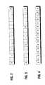
- FIG. 2is a depiction of a cell in accordance with one embodiment of the present invention.
- FIG. 3is a depiction of another cell in accordance with another embodiment of the present invention.
- FIG. 4is a depiction of still another cell in accordance with one embodiment of the present invention.
- FIG. 5is a flow chart for software in accordance with one embodiment of the present invention.
- a processor 100may be coupled through a bus 102 to a multi-level cell memory 104 .
- the memory 104contains an interface controller 105 , a write state machine 106 and a multi-level cell memory array 150 .
- the processor 100is coupled by the bus 102 to both the interface controller 105 and the memory array 150 in one embodiment of the present invention.
- the interface controller 105provides control over the multi-level cell memory array 150 .
- the write state machine 106communicates with the interface controller 105 and the memory array 150 .
- the interface controller 105passes data to be written into the array 150 to the state machine 106 .
- the state machine 106executes a sequence of events to write data into the array 150 .
- the interface controller 105 , the write state machine 106 and the multi-level cell memory array 150are located on a single integrated circuit die.
- any number of bitsmay be stored in a single cell, for example, by increasing the number of threshold levels, without deviating from the spirit and scope of the present invention.
- embodiments of the present inventionare described in conjunction with a memory array 150 of flash cells, other cells such as read only memory (ROM), erasable programmable read only memory (EPROM) conventional electrically erasable programmable read only memory (EEPROM), or dynamic random access memory (DRAM), to mention a few examples, may be substituted without deviating from the spirit and scope of the present invention.
- ROMread only memory
- EPROMerasable programmable read only memory
- EEPROMelectrically erasable programmable read only memory
- DRAMdynamic random access memory
- a cellmay include only one bit of data at the first and last states of the cell.
- the actual storage of datais indicated by an X and empty states are indicated by dashes.
- a similarly sized cell, shown in FIG. 3may store two bits per cell at every fifth level within the cell.
- the same sized cellmay store four bits per cell using every single state or level of the sixteen available states in this example.
- the number of bits per cellmay be changed to increase the fidelity of the stored data.
- the scheme shown in FIG. 4 or other higher density schemesmay be utilized.
- the datamay be spread in the cell, decreasing the density per cell and increasing the number of cells required to store all of the data.
- the integrity of the data storagewill be improved. This is because it is easier to discern the differential voltage between significantly nonadjacent levels. In fact, the greater the distance between the levels, the easier it is to discern a differential voltage.
- datamay be stored in varying numbers of bits per cell depending on the type of data involved.
- some datamay be packed closely as indicated for example in FIG. 4 and other data may be spread farther apart, requiring additional numbers of cells to complete the data storage.
- the write algorithm 122which may be implemented in software or hardware, initially identifies the number of bits per cell.
- the number of bits per cellmay be derived from information included with the data indicating the desired fidelity. Based on the number of bits per cell, the packing of bits into each given cell may be adjusted. Thus, in some cases, denser packing may be utilized, for example as shown in FIG. 4 , and in other cases, looser or more spread apart packing may be utilized as shown in FIG. 2 .
- the packing of bits into each cellis adjusted as indicated in block 126 .
- the bitsare written to the cells as indicated in block 128 .
- the number of bits per cellmay be changed on the fly from cell to cell.
- the read processsimply reverses the flow, ignoring the missing levels, and simply reading the actual data out of each cell.
- the spread apart datamay then be repacked into a continuous data string.
Landscapes
- Engineering & Computer Science (AREA)
- Computer Hardware Design (AREA)
- Read Only Memory (AREA)
- Circuits Of Receivers In General (AREA)
- Control Of Indicators Other Than Cathode Ray Tubes (AREA)
- Techniques For Improving Reliability Of Storages (AREA)
Abstract
Description
Claims (18)
Priority Applications (1)
| Application Number | Priority Date | Filing Date | Title |
|---|---|---|---|
| US10/666,988US6870767B2 (en) | 2001-09-18 | 2003-09-18 | Variable level memory |
Applications Claiming Priority (2)
| Application Number | Priority Date | Filing Date | Title |
|---|---|---|---|
| US09/955,282US6643169B2 (en) | 2001-09-18 | 2001-09-18 | Variable level memory |
| US10/666,988US6870767B2 (en) | 2001-09-18 | 2003-09-18 | Variable level memory |
Related Parent Applications (1)
| Application Number | Title | Priority Date | Filing Date |
|---|---|---|---|
| US09/955,282ContinuationUS6643169B2 (en) | 2001-09-18 | 2001-09-18 | Variable level memory |
Publications (2)
| Publication Number | Publication Date |
|---|---|
| US20040057355A1 US20040057355A1 (en) | 2004-03-25 |
| US6870767B2true US6870767B2 (en) | 2005-03-22 |
Family
ID=25496611
Family Applications (2)
| Application Number | Title | Priority Date | Filing Date |
|---|---|---|---|
| US09/955,282Expired - LifetimeUS6643169B2 (en) | 2001-09-18 | 2001-09-18 | Variable level memory |
| US10/666,988Expired - LifetimeUS6870767B2 (en) | 2001-09-18 | 2003-09-18 | Variable level memory |
Family Applications Before (1)
| Application Number | Title | Priority Date | Filing Date |
|---|---|---|---|
| US09/955,282Expired - LifetimeUS6643169B2 (en) | 2001-09-18 | 2001-09-18 | Variable level memory |
Country Status (8)
| Country | Link |
|---|---|
| US (2) | US6643169B2 (en) |
| EP (1) | EP1428221B1 (en) |
| KR (1) | KR100580017B1 (en) |
| CN (1) | CN100585737C (en) |
| AT (1) | ATE365967T1 (en) |
| DE (1) | DE60220931T2 (en) |
| TW (1) | TWI268511B (en) |
| WO (1) | WO2003025948A1 (en) |
Cited By (73)
| Publication number | Priority date | Publication date | Assignee | Title |
|---|---|---|---|---|
| US20060220639A1 (en)* | 2005-03-30 | 2006-10-05 | Impinj, Inc. | Fault tolerant non volatile memories and methods |
| US20070002613A1 (en)* | 2005-06-30 | 2007-01-04 | Intel Corporation | Memory array with pseudo single bit memory cell and method |
| US20080148115A1 (en)* | 2006-12-17 | 2008-06-19 | Anobit Technologies Ltd. | High-speed programming of memory devices |
| US20080158958A1 (en)* | 2006-12-17 | 2008-07-03 | Anobit Technologies Ltd. | Memory device with reduced reading |
| US20080181001A1 (en)* | 2007-01-24 | 2008-07-31 | Anobit Technologies | Memory device with negative thresholds |
| US20080219050A1 (en)* | 2007-01-24 | 2008-09-11 | Anobit Technologies Ltd. | Reduction of back pattern dependency effects in memory devices |
| US20080263262A1 (en)* | 2007-04-22 | 2008-10-23 | Anobit Technologies Ltd. | Command interface for memory devices |
| US20080282106A1 (en)* | 2007-05-12 | 2008-11-13 | Anobit Technologies Ltd | Data storage with incremental redundancy |
| US20090024905A1 (en)* | 2006-05-12 | 2009-01-22 | Anobit Technologies Ltd. | Combined distortion estimation and error correction coding for memory devices |
| US20090046509A1 (en)* | 2007-08-17 | 2009-02-19 | Ravi Annavajjhala | Technique to improve and extend endurance and reliability of multi-level memory cells in a memory device |
| US20090106485A1 (en)* | 2007-10-19 | 2009-04-23 | Anobit Technologies Ltd. | Reading analog memory cells using built-in multi-threshold commands |
| US20090103358A1 (en)* | 2006-05-12 | 2009-04-23 | Anobit Technologies Ltd. | Reducing programming error in memory devices |
| US20090158126A1 (en)* | 2007-12-12 | 2009-06-18 | Anobit Technologies Ltd | Efficient interference cancellation in analog memory cell arrays |
| US20090168524A1 (en)* | 2007-12-27 | 2009-07-02 | Anobit Technologies Ltd. | Wear level estimation in analog memory cells |
| US20090199074A1 (en)* | 2008-02-05 | 2009-08-06 | Anobit Technologies Ltd. | Parameter estimation based on error correction code parity check equations |
| US20090213653A1 (en)* | 2008-02-21 | 2009-08-27 | Anobit Technologies Ltd | Programming of analog memory cells using a single programming pulse per state transition |
| US20090228761A1 (en)* | 2008-03-07 | 2009-09-10 | Anobit Technologies Ltd | Efficient readout from analog memory cells using data compression |
| US20090240872A1 (en)* | 2008-03-18 | 2009-09-24 | Anobit Technologies Ltd | Memory device with multiple-accuracy read commands |
| US7679957B2 (en) | 2005-03-31 | 2010-03-16 | Virage Logic Corporation | Redundant non-volatile memory cell |
| US20100091535A1 (en)* | 2007-03-12 | 2010-04-15 | Anobit Technologies Ltd | Adaptive estimation of memory cell read thresholds |
| US20100115376A1 (en)* | 2006-12-03 | 2010-05-06 | Anobit Technologies Ltd. | Automatic defect management in memory devices |
| US7719896B1 (en) | 2007-04-24 | 2010-05-18 | Virage Logic Corporation | Configurable single bit/dual bits memory |
| US20100124088A1 (en)* | 2008-11-16 | 2010-05-20 | Anobit Technologies Ltd | Storage at m bits/cell density in n bits/cell analog memory cell devices, m>n |
| US20100157641A1 (en)* | 2006-05-12 | 2010-06-24 | Anobit Technologies Ltd. | Memory device with adaptive capacity |
| US20100157675A1 (en)* | 2007-09-19 | 2010-06-24 | Anobit Technologies Ltd | Programming orders for reducing distortion in arrays of multi-level analog memory cells |
| US20100165689A1 (en)* | 2008-12-31 | 2010-07-01 | Anobit Technologies Ltd | Rejuvenation of analog memory cells |
| US20100199150A1 (en)* | 2007-10-19 | 2010-08-05 | Anobit Technologies Ltd | Data Storage In Analog Memory Cell Arrays Having Erase Failures |
| US7773413B2 (en) | 2007-10-08 | 2010-08-10 | Anobit Technologies Ltd. | Reliable data storage in analog memory cells in the presence of temperature variations |
| US20100220510A1 (en)* | 2007-11-13 | 2010-09-02 | Anobit Technologies Ltd | Optimized Selection of Memory Chips in Multi-Chips Memory Devices |
| US7791950B2 (en) | 2005-03-17 | 2010-09-07 | Virage Logic Corporation | Inverter non-volatile memory cell and array system |
| US20100250836A1 (en)* | 2009-03-25 | 2010-09-30 | Anobit Technologies Ltd | Use of Host System Resources by Memory Controller |
| US7821826B2 (en) | 2006-10-30 | 2010-10-26 | Anobit Technologies, Ltd. | Memory cell readout using successive approximation |
| US7864573B2 (en) | 2008-02-24 | 2011-01-04 | Anobit Technologies Ltd. | Programming analog memory cells for reduced variance after retention |
| US7920423B1 (en) | 2007-07-31 | 2011-04-05 | Synopsys, Inc. | Non volatile memory circuit with tailored reliability |
| US7925936B1 (en) | 2007-07-13 | 2011-04-12 | Anobit Technologies Ltd. | Memory device with non-uniform programming levels |
| US7924648B2 (en) | 2006-11-28 | 2011-04-12 | Anobit Technologies Ltd. | Memory power and performance management |
| US7924613B1 (en) | 2008-08-05 | 2011-04-12 | Anobit Technologies Ltd. | Data storage in analog memory cells with protection against programming interruption |
| US7975192B2 (en) | 2006-10-30 | 2011-07-05 | Anobit Technologies Ltd. | Reading memory cells using multiple thresholds |
| US7995388B1 (en) | 2008-08-05 | 2011-08-09 | Anobit Technologies Ltd. | Data storage using modified voltages |
| US8000135B1 (en) | 2008-09-14 | 2011-08-16 | Anobit Technologies Ltd. | Estimation of memory cell read thresholds by sampling inside programming level distribution intervals |
| US8000141B1 (en) | 2007-10-19 | 2011-08-16 | Anobit Technologies Ltd. | Compensation for voltage drifts in analog memory cells |
| US8050086B2 (en) | 2006-05-12 | 2011-11-01 | Anobit Technologies Ltd. | Distortion estimation and cancellation in memory devices |
| US8060806B2 (en) | 2006-08-27 | 2011-11-15 | Anobit Technologies Ltd. | Estimation of non-linear distortion in memory devices |
| US8169825B1 (en) | 2008-09-02 | 2012-05-01 | Anobit Technologies Ltd. | Reliable data storage in analog memory cells subjected to long retention periods |
| US8174857B1 (en) | 2008-12-31 | 2012-05-08 | Anobit Technologies Ltd. | Efficient readout schemes for analog memory cell devices using multiple read threshold sets |
| US8225181B2 (en) | 2007-11-30 | 2012-07-17 | Apple Inc. | Efficient re-read operations from memory devices |
| US8228701B2 (en) | 2009-03-01 | 2012-07-24 | Apple Inc. | Selective activation of programming schemes in analog memory cell arrays |
| US8239734B1 (en) | 2008-10-15 | 2012-08-07 | Apple Inc. | Efficient data storage in storage device arrays |
| US8238157B1 (en) | 2009-04-12 | 2012-08-07 | Apple Inc. | Selective re-programming of analog memory cells |
| US8259506B1 (en) | 2009-03-25 | 2012-09-04 | Apple Inc. | Database of memory read thresholds |
| US8261159B1 (en) | 2008-10-30 | 2012-09-04 | Apple, Inc. | Data scrambling schemes for memory devices |
| US8259497B2 (en) | 2007-08-06 | 2012-09-04 | Apple Inc. | Programming schemes for multi-level analog memory cells |
| US8400858B2 (en) | 2008-03-18 | 2013-03-19 | Apple Inc. | Memory device with reduced sense time readout |
| US8429493B2 (en) | 2007-05-12 | 2013-04-23 | Apple Inc. | Memory device with internal signap processing unit |
| US8456905B2 (en) | 2007-12-16 | 2013-06-04 | Apple Inc. | Efficient data storage in multi-plane memory devices |
| US8479080B1 (en) | 2009-07-12 | 2013-07-02 | Apple Inc. | Adaptive over-provisioning in memory systems |
| US8482978B1 (en) | 2008-09-14 | 2013-07-09 | Apple Inc. | Estimation of memory cell read thresholds by sampling inside programming level distribution intervals |
| US8495465B1 (en) | 2009-10-15 | 2013-07-23 | Apple Inc. | Error correction coding over multiple memory pages |
| US8572423B1 (en) | 2010-06-22 | 2013-10-29 | Apple Inc. | Reducing peak current in memory systems |
| US8572311B1 (en) | 2010-01-11 | 2013-10-29 | Apple Inc. | Redundant data storage in multi-die memory systems |
| US8595591B1 (en) | 2010-07-11 | 2013-11-26 | Apple Inc. | Interference-aware assignment of programming levels in analog memory cells |
| US8645794B1 (en) | 2010-07-31 | 2014-02-04 | Apple Inc. | Data storage in analog memory cells using a non-integer number of bits per cell |
| US8677054B1 (en) | 2009-12-16 | 2014-03-18 | Apple Inc. | Memory management schemes for non-volatile memory devices |
| US8694854B1 (en) | 2010-08-17 | 2014-04-08 | Apple Inc. | Read threshold setting based on soft readout statistics |
| US8694853B1 (en) | 2010-05-04 | 2014-04-08 | Apple Inc. | Read commands for reading interfering memory cells |
| US8694814B1 (en) | 2010-01-10 | 2014-04-08 | Apple Inc. | Reuse of host hibernation storage space by memory controller |
| US8856475B1 (en) | 2010-08-01 | 2014-10-07 | Apple Inc. | Efficient selection of memory blocks for compaction |
| US8924661B1 (en) | 2009-01-18 | 2014-12-30 | Apple Inc. | Memory system including a controller and processors associated with memory devices |
| US8949684B1 (en) | 2008-09-02 | 2015-02-03 | Apple Inc. | Segmented data storage |
| US9021181B1 (en) | 2010-09-27 | 2015-04-28 | Apple Inc. | Memory management for unifying memory cell conditions by using maximum time intervals |
| US9104580B1 (en) | 2010-07-27 | 2015-08-11 | Apple Inc. | Cache memory for hybrid disk drives |
| US11556416B2 (en) | 2021-05-05 | 2023-01-17 | Apple Inc. | Controlling memory readout reliability and throughput by adjusting distance between read thresholds |
| US11847342B2 (en) | 2021-07-28 | 2023-12-19 | Apple Inc. | Efficient transfer of hard data and confidence levels in reading a nonvolatile memory |
Families Citing this family (25)
| Publication number | Priority date | Publication date | Assignee | Title |
|---|---|---|---|---|
| US7554842B2 (en)* | 2001-09-17 | 2009-06-30 | Sandisk Corporation | Multi-purpose non-volatile memory card |
| US7178004B2 (en)* | 2003-01-31 | 2007-02-13 | Yan Polansky | Memory array programming circuit and a method for using the circuit |
| US7117326B2 (en)* | 2003-06-26 | 2006-10-03 | Intel Corporation | Tracking modifications to a memory |
| US7356755B2 (en)* | 2003-10-16 | 2008-04-08 | Intel Corporation | Error correction for multi-level cell memory with overwrite capability |
| US7639542B2 (en)* | 2006-05-15 | 2009-12-29 | Apple Inc. | Maintenance operations for multi-level data storage cells |
| US7613043B2 (en) | 2006-05-15 | 2009-11-03 | Apple Inc. | Shifting reference values to account for voltage sag |
| US7568135B2 (en) | 2006-05-15 | 2009-07-28 | Apple Inc. | Use of alternative value in cell detection |
| US8000134B2 (en) | 2006-05-15 | 2011-08-16 | Apple Inc. | Off-die charge pump that supplies multiple flash devices |
| US7646636B2 (en) | 2007-02-16 | 2010-01-12 | Mosaid Technologies Incorporated | Non-volatile memory with dynamic multi-mode operation |
| US7958301B2 (en)* | 2007-04-10 | 2011-06-07 | Marvell World Trade Ltd. | Memory controller and method for memory pages with dynamically configurable bits per cell |
| US20090055605A1 (en) | 2007-08-20 | 2009-02-26 | Zining Wu | Method and system for object-oriented data storage |
| US8583857B2 (en)* | 2007-08-20 | 2013-11-12 | Marvell World Trade Ltd. | Method and system for object-oriented data storage |
| KR20100010355A (en) | 2008-07-22 | 2010-02-01 | 삼성전자주식회사 | Multi-bit flash memory device and program and erase methods for the same |
| US20110173462A1 (en)* | 2010-01-11 | 2011-07-14 | Apple Inc. | Controlling and staggering operations to limit current spikes |
| US8773925B2 (en) | 2010-02-23 | 2014-07-08 | Rambus Inc. | Multilevel DRAM |
| US8402243B2 (en) | 2010-02-25 | 2013-03-19 | Apple Inc. | Dynamically allocating number of bits per cell for memory locations of a non-volatile memory |
| US8089807B1 (en)* | 2010-11-22 | 2012-01-03 | Ge Aviation Systems, Llc | Method and system for data storage |
| US20120140556A1 (en)* | 2010-12-07 | 2012-06-07 | Macronix International Co., Ltd. | Method of operating flash memory |
| KR20130060791A (en)* | 2011-11-30 | 2013-06-10 | 삼성전자주식회사 | Memory system, data storage device, memory card, and ssd including wear level control logic |
| KR101949987B1 (en)* | 2012-12-18 | 2019-02-20 | 에스케이하이닉스 주식회사 | Data storage device and operating method thereof |
| WO2014120660A1 (en) | 2013-01-29 | 2014-08-07 | Marvell World Trade Ltd. | Methods and apparatus for storing data to a solid state storage device based on data classification |
| US9047211B2 (en) | 2013-03-15 | 2015-06-02 | SanDisk Technologies, Inc. | Managing data reliability |
| US9690656B2 (en)* | 2015-02-27 | 2017-06-27 | Microsoft Technology Licensing, Llc | Data encoding on single-level and variable multi-level cell storage |
| US9786386B2 (en) | 2015-02-27 | 2017-10-10 | Microsoft Technology Licensing, Llc | Dynamic approximate storage for custom applications |
| US11081168B2 (en)* | 2019-05-23 | 2021-08-03 | Hefei Reliance Memory Limited | Mixed digital-analog memory devices and circuits for secure storage and computing |
Citations (5)
| Publication number | Priority date | Publication date | Assignee | Title |
|---|---|---|---|---|
| US5828601A (en)* | 1993-12-01 | 1998-10-27 | Advanced Micro Devices, Inc. | Programmed reference |
| US6205057B1 (en)* | 2000-02-15 | 2001-03-20 | Advanced Micro Devices | System and method for detecting flash memory threshold voltages |
| US6215697B1 (en)* | 1999-01-14 | 2001-04-10 | Macronix International Co., Ltd. | Multi-level memory cell device and method for self-converged programming |
| US6396742B1 (en)* | 2000-07-28 | 2002-05-28 | Silicon Storage Technology, Inc. | Testing of multilevel semiconductor memory |
| US6522586B2 (en)* | 2000-04-25 | 2003-02-18 | Multi Level Memory Technology | Dynamic refresh that changes the physical storage locations of data in flash memory |
Family Cites Families (7)
| Publication number | Priority date | Publication date | Assignee | Title |
|---|---|---|---|---|
| US5424978A (en)* | 1993-03-15 | 1995-06-13 | Nippon Steel Corporation | Non-volatile semiconductor memory cell capable of storing more than two different data and method of using the same |
| US5515317A (en)* | 1994-06-02 | 1996-05-07 | Intel Corporation | Addressing modes for a dynamic single bit per cell to multiple bit per cell memory |
| WO1995034074A1 (en) | 1994-06-02 | 1995-12-14 | Intel Corporation | Dynamic single to multiple bit per cell memory |
| JPH09102190A (en) | 1995-08-02 | 1997-04-15 | Sanyo Electric Co Ltd | Signal recording device, and signal reading device, and signal recording and reading device |
| DE69635105D1 (en) | 1996-01-31 | 2005-09-29 | St Microelectronics Srl | Multi-stage memory circuits and corresponding reading and writing methods |
| KR100327421B1 (en)* | 1997-12-31 | 2002-07-27 | 주식회사 하이닉스반도체 | Program System of Nonvolatile Memory Device and Its Program Method |
| US6363008B1 (en)* | 2000-02-17 | 2002-03-26 | Multi Level Memory Technology | Multi-bit-cell non-volatile memory with maximized data capacity |
- 2001
- 2001-09-18USUS09/955,282patent/US6643169B2/ennot_activeExpired - Lifetime
- 2002
- 2002-08-06DEDE60220931Tpatent/DE60220931T2/ennot_activeExpired - Lifetime
- 2002-08-06CNCN02822880Apatent/CN100585737C/ennot_activeExpired - Lifetime
- 2002-08-06EPEP02757016Apatent/EP1428221B1/ennot_activeExpired - Lifetime
- 2002-08-06KRKR1020047003885Apatent/KR100580017B1/ennot_activeExpired - Lifetime
- 2002-08-06ATAT02757016Tpatent/ATE365967T1/ennot_activeIP Right Cessation
- 2002-08-06WOPCT/US2002/025092patent/WO2003025948A1/enactiveIP Right Grant
- 2002-08-28TWTW091119529Apatent/TWI268511B/ennot_activeIP Right Cessation
- 2003
- 2003-09-18USUS10/666,988patent/US6870767B2/ennot_activeExpired - Lifetime
Patent Citations (5)
| Publication number | Priority date | Publication date | Assignee | Title |
|---|---|---|---|---|
| US5828601A (en)* | 1993-12-01 | 1998-10-27 | Advanced Micro Devices, Inc. | Programmed reference |
| US6215697B1 (en)* | 1999-01-14 | 2001-04-10 | Macronix International Co., Ltd. | Multi-level memory cell device and method for self-converged programming |
| US6205057B1 (en)* | 2000-02-15 | 2001-03-20 | Advanced Micro Devices | System and method for detecting flash memory threshold voltages |
| US6522586B2 (en)* | 2000-04-25 | 2003-02-18 | Multi Level Memory Technology | Dynamic refresh that changes the physical storage locations of data in flash memory |
| US6396742B1 (en)* | 2000-07-28 | 2002-05-28 | Silicon Storage Technology, Inc. | Testing of multilevel semiconductor memory |
Cited By (114)
| Publication number | Priority date | Publication date | Assignee | Title |
|---|---|---|---|---|
| US7791950B2 (en) | 2005-03-17 | 2010-09-07 | Virage Logic Corporation | Inverter non-volatile memory cell and array system |
| US7715236B2 (en) | 2005-03-30 | 2010-05-11 | Virage Logic Corporation | Fault tolerant non volatile memories and methods |
| US20060220639A1 (en)* | 2005-03-30 | 2006-10-05 | Impinj, Inc. | Fault tolerant non volatile memories and methods |
| US7808823B2 (en) | 2005-03-31 | 2010-10-05 | Virage Logic Corporation | RFID tag with redundant non-volatile memory cell |
| US7679957B2 (en) | 2005-03-31 | 2010-03-16 | Virage Logic Corporation | Redundant non-volatile memory cell |
| US7272041B2 (en) | 2005-06-30 | 2007-09-18 | Intel Corporation | Memory array with pseudo single bit memory cell and method |
| US7525840B2 (en) | 2005-06-30 | 2009-04-28 | Intel Corporation | Memory array with pseudo single bit memory cell and method |
| US20070002613A1 (en)* | 2005-06-30 | 2007-01-04 | Intel Corporation | Memory array with pseudo single bit memory cell and method |
| US8156403B2 (en) | 2006-05-12 | 2012-04-10 | Anobit Technologies Ltd. | Combined distortion estimation and error correction coding for memory devices |
| US20090024905A1 (en)* | 2006-05-12 | 2009-01-22 | Anobit Technologies Ltd. | Combined distortion estimation and error correction coding for memory devices |
| US20100157641A1 (en)* | 2006-05-12 | 2010-06-24 | Anobit Technologies Ltd. | Memory device with adaptive capacity |
| US8239735B2 (en) | 2006-05-12 | 2012-08-07 | Apple Inc. | Memory Device with adaptive capacity |
| US20090103358A1 (en)* | 2006-05-12 | 2009-04-23 | Anobit Technologies Ltd. | Reducing programming error in memory devices |
| US8050086B2 (en) | 2006-05-12 | 2011-11-01 | Anobit Technologies Ltd. | Distortion estimation and cancellation in memory devices |
| US8599611B2 (en) | 2006-05-12 | 2013-12-03 | Apple Inc. | Distortion estimation and cancellation in memory devices |
| US8570804B2 (en) | 2006-05-12 | 2013-10-29 | Apple Inc. | Distortion estimation and cancellation in memory devices |
| US7697326B2 (en) | 2006-05-12 | 2010-04-13 | Anobit Technologies Ltd. | Reducing programming error in memory devices |
| US8060806B2 (en) | 2006-08-27 | 2011-11-15 | Anobit Technologies Ltd. | Estimation of non-linear distortion in memory devices |
| US8145984B2 (en) | 2006-10-30 | 2012-03-27 | Anobit Technologies Ltd. | Reading memory cells using multiple thresholds |
| US20110225472A1 (en)* | 2006-10-30 | 2011-09-15 | Anobit Technologies Ltd. | Reading memory cells using multiple thresholds |
| USRE46346E1 (en) | 2006-10-30 | 2017-03-21 | Apple Inc. | Reading memory cells using multiple thresholds |
| US7821826B2 (en) | 2006-10-30 | 2010-10-26 | Anobit Technologies, Ltd. | Memory cell readout using successive approximation |
| US7975192B2 (en) | 2006-10-30 | 2011-07-05 | Anobit Technologies Ltd. | Reading memory cells using multiple thresholds |
| US7924648B2 (en) | 2006-11-28 | 2011-04-12 | Anobit Technologies Ltd. | Memory power and performance management |
| US8151163B2 (en) | 2006-12-03 | 2012-04-03 | Anobit Technologies Ltd. | Automatic defect management in memory devices |
| US20100115376A1 (en)* | 2006-12-03 | 2010-05-06 | Anobit Technologies Ltd. | Automatic defect management in memory devices |
| US7900102B2 (en) | 2006-12-17 | 2011-03-01 | Anobit Technologies Ltd. | High-speed programming of memory devices |
| US20080148115A1 (en)* | 2006-12-17 | 2008-06-19 | Anobit Technologies Ltd. | High-speed programming of memory devices |
| US20080158958A1 (en)* | 2006-12-17 | 2008-07-03 | Anobit Technologies Ltd. | Memory device with reduced reading |
| US7593263B2 (en) | 2006-12-17 | 2009-09-22 | Anobit Technologies Ltd. | Memory device with reduced reading latency |
| US20100195390A1 (en)* | 2007-01-24 | 2010-08-05 | Anobit Technologies Ltd | Memory device with negative thresholds |
| US7881107B2 (en) | 2007-01-24 | 2011-02-01 | Anobit Technologies Ltd. | Memory device with negative thresholds |
| US7751240B2 (en) | 2007-01-24 | 2010-07-06 | Anobit Technologies Ltd. | Memory device with negative thresholds |
| US20080181001A1 (en)* | 2007-01-24 | 2008-07-31 | Anobit Technologies | Memory device with negative thresholds |
| US8151166B2 (en) | 2007-01-24 | 2012-04-03 | Anobit Technologies Ltd. | Reduction of back pattern dependency effects in memory devices |
| US20080219050A1 (en)* | 2007-01-24 | 2008-09-11 | Anobit Technologies Ltd. | Reduction of back pattern dependency effects in memory devices |
| US20100091535A1 (en)* | 2007-03-12 | 2010-04-15 | Anobit Technologies Ltd | Adaptive estimation of memory cell read thresholds |
| US8369141B2 (en) | 2007-03-12 | 2013-02-05 | Apple Inc. | Adaptive estimation of memory cell read thresholds |
| US8001320B2 (en) | 2007-04-22 | 2011-08-16 | Anobit Technologies Ltd. | Command interface for memory devices |
| US20080263262A1 (en)* | 2007-04-22 | 2008-10-23 | Anobit Technologies Ltd. | Command interface for memory devices |
| US7796450B1 (en) | 2007-04-24 | 2010-09-14 | Virage Logic Corporation | Radio frequency (RFID) tag including configurable single bit/dual bits memory |
| US7719896B1 (en) | 2007-04-24 | 2010-05-18 | Virage Logic Corporation | Configurable single bit/dual bits memory |
| US20080282106A1 (en)* | 2007-05-12 | 2008-11-13 | Anobit Technologies Ltd | Data storage with incremental redundancy |
| US8234545B2 (en) | 2007-05-12 | 2012-07-31 | Apple Inc. | Data storage with incremental redundancy |
| US8429493B2 (en) | 2007-05-12 | 2013-04-23 | Apple Inc. | Memory device with internal signap processing unit |
| US7925936B1 (en) | 2007-07-13 | 2011-04-12 | Anobit Technologies Ltd. | Memory device with non-uniform programming levels |
| US7920423B1 (en) | 2007-07-31 | 2011-04-05 | Synopsys, Inc. | Non volatile memory circuit with tailored reliability |
| US8259497B2 (en) | 2007-08-06 | 2012-09-04 | Apple Inc. | Programming schemes for multi-level analog memory cells |
| US20090046509A1 (en)* | 2007-08-17 | 2009-02-19 | Ravi Annavajjhala | Technique to improve and extend endurance and reliability of multi-level memory cells in a memory device |
| US7802132B2 (en)* | 2007-08-17 | 2010-09-21 | Intel Corporation | Technique to improve and extend endurance and reliability of multi-level memory cells in a memory device |
| US20100157675A1 (en)* | 2007-09-19 | 2010-06-24 | Anobit Technologies Ltd | Programming orders for reducing distortion in arrays of multi-level analog memory cells |
| US8174905B2 (en) | 2007-09-19 | 2012-05-08 | Anobit Technologies Ltd. | Programming orders for reducing distortion in arrays of multi-level analog memory cells |
| US7773413B2 (en) | 2007-10-08 | 2010-08-10 | Anobit Technologies Ltd. | Reliable data storage in analog memory cells in the presence of temperature variations |
| US8000141B1 (en) | 2007-10-19 | 2011-08-16 | Anobit Technologies Ltd. | Compensation for voltage drifts in analog memory cells |
| US8527819B2 (en) | 2007-10-19 | 2013-09-03 | Apple Inc. | Data storage in analog memory cell arrays having erase failures |
| US20100199150A1 (en)* | 2007-10-19 | 2010-08-05 | Anobit Technologies Ltd | Data Storage In Analog Memory Cell Arrays Having Erase Failures |
| US20090106485A1 (en)* | 2007-10-19 | 2009-04-23 | Anobit Technologies Ltd. | Reading analog memory cells using built-in multi-threshold commands |
| US8068360B2 (en) | 2007-10-19 | 2011-11-29 | Anobit Technologies Ltd. | Reading analog memory cells using built-in multi-threshold commands |
| US20100220510A1 (en)* | 2007-11-13 | 2010-09-02 | Anobit Technologies Ltd | Optimized Selection of Memory Chips in Multi-Chips Memory Devices |
| US8270246B2 (en) | 2007-11-13 | 2012-09-18 | Apple Inc. | Optimized selection of memory chips in multi-chips memory devices |
| US8225181B2 (en) | 2007-11-30 | 2012-07-17 | Apple Inc. | Efficient re-read operations from memory devices |
| US8209588B2 (en) | 2007-12-12 | 2012-06-26 | Anobit Technologies Ltd. | Efficient interference cancellation in analog memory cell arrays |
| US20090158126A1 (en)* | 2007-12-12 | 2009-06-18 | Anobit Technologies Ltd | Efficient interference cancellation in analog memory cell arrays |
| US8456905B2 (en) | 2007-12-16 | 2013-06-04 | Apple Inc. | Efficient data storage in multi-plane memory devices |
| US8085586B2 (en) | 2007-12-27 | 2011-12-27 | Anobit Technologies Ltd. | Wear level estimation in analog memory cells |
| US20090168524A1 (en)* | 2007-12-27 | 2009-07-02 | Anobit Technologies Ltd. | Wear level estimation in analog memory cells |
| US20090199074A1 (en)* | 2008-02-05 | 2009-08-06 | Anobit Technologies Ltd. | Parameter estimation based on error correction code parity check equations |
| US8156398B2 (en) | 2008-02-05 | 2012-04-10 | Anobit Technologies Ltd. | Parameter estimation based on error correction code parity check equations |
| US20090213653A1 (en)* | 2008-02-21 | 2009-08-27 | Anobit Technologies Ltd | Programming of analog memory cells using a single programming pulse per state transition |
| US7924587B2 (en) | 2008-02-21 | 2011-04-12 | Anobit Technologies Ltd. | Programming of analog memory cells using a single programming pulse per state transition |
| US7864573B2 (en) | 2008-02-24 | 2011-01-04 | Anobit Technologies Ltd. | Programming analog memory cells for reduced variance after retention |
| US8230300B2 (en) | 2008-03-07 | 2012-07-24 | Apple Inc. | Efficient readout from analog memory cells using data compression |
| US20090228761A1 (en)* | 2008-03-07 | 2009-09-10 | Anobit Technologies Ltd | Efficient readout from analog memory cells using data compression |
| US8400858B2 (en) | 2008-03-18 | 2013-03-19 | Apple Inc. | Memory device with reduced sense time readout |
| US8059457B2 (en) | 2008-03-18 | 2011-11-15 | Anobit Technologies Ltd. | Memory device with multiple-accuracy read commands |
| US20090240872A1 (en)* | 2008-03-18 | 2009-09-24 | Anobit Technologies Ltd | Memory device with multiple-accuracy read commands |
| US7995388B1 (en) | 2008-08-05 | 2011-08-09 | Anobit Technologies Ltd. | Data storage using modified voltages |
| US7924613B1 (en) | 2008-08-05 | 2011-04-12 | Anobit Technologies Ltd. | Data storage in analog memory cells with protection against programming interruption |
| US8498151B1 (en) | 2008-08-05 | 2013-07-30 | Apple Inc. | Data storage in analog memory cells using modified pass voltages |
| US8169825B1 (en) | 2008-09-02 | 2012-05-01 | Anobit Technologies Ltd. | Reliable data storage in analog memory cells subjected to long retention periods |
| US8949684B1 (en) | 2008-09-02 | 2015-02-03 | Apple Inc. | Segmented data storage |
| US8482978B1 (en) | 2008-09-14 | 2013-07-09 | Apple Inc. | Estimation of memory cell read thresholds by sampling inside programming level distribution intervals |
| US8000135B1 (en) | 2008-09-14 | 2011-08-16 | Anobit Technologies Ltd. | Estimation of memory cell read thresholds by sampling inside programming level distribution intervals |
| US8239734B1 (en) | 2008-10-15 | 2012-08-07 | Apple Inc. | Efficient data storage in storage device arrays |
| US8261159B1 (en) | 2008-10-30 | 2012-09-04 | Apple, Inc. | Data scrambling schemes for memory devices |
| US20100124088A1 (en)* | 2008-11-16 | 2010-05-20 | Anobit Technologies Ltd | Storage at m bits/cell density in n bits/cell analog memory cell devices, m>n |
| US8208304B2 (en) | 2008-11-16 | 2012-06-26 | Anobit Technologies Ltd. | Storage at M bits/cell density in N bits/cell analog memory cell devices, M>N |
| US20100165689A1 (en)* | 2008-12-31 | 2010-07-01 | Anobit Technologies Ltd | Rejuvenation of analog memory cells |
| US8397131B1 (en) | 2008-12-31 | 2013-03-12 | Apple Inc. | Efficient readout schemes for analog memory cell devices |
| US8174857B1 (en) | 2008-12-31 | 2012-05-08 | Anobit Technologies Ltd. | Efficient readout schemes for analog memory cell devices using multiple read threshold sets |
| US8248831B2 (en) | 2008-12-31 | 2012-08-21 | Apple Inc. | Rejuvenation of analog memory cells |
| US8924661B1 (en) | 2009-01-18 | 2014-12-30 | Apple Inc. | Memory system including a controller and processors associated with memory devices |
| US8228701B2 (en) | 2009-03-01 | 2012-07-24 | Apple Inc. | Selective activation of programming schemes in analog memory cell arrays |
| US20100250836A1 (en)* | 2009-03-25 | 2010-09-30 | Anobit Technologies Ltd | Use of Host System Resources by Memory Controller |
| US8832354B2 (en) | 2009-03-25 | 2014-09-09 | Apple Inc. | Use of host system resources by memory controller |
| US8259506B1 (en) | 2009-03-25 | 2012-09-04 | Apple Inc. | Database of memory read thresholds |
| US8238157B1 (en) | 2009-04-12 | 2012-08-07 | Apple Inc. | Selective re-programming of analog memory cells |
| US8479080B1 (en) | 2009-07-12 | 2013-07-02 | Apple Inc. | Adaptive over-provisioning in memory systems |
| US8495465B1 (en) | 2009-10-15 | 2013-07-23 | Apple Inc. | Error correction coding over multiple memory pages |
| US8677054B1 (en) | 2009-12-16 | 2014-03-18 | Apple Inc. | Memory management schemes for non-volatile memory devices |
| US8694814B1 (en) | 2010-01-10 | 2014-04-08 | Apple Inc. | Reuse of host hibernation storage space by memory controller |
| US8572311B1 (en) | 2010-01-11 | 2013-10-29 | Apple Inc. | Redundant data storage in multi-die memory systems |
| US8677203B1 (en) | 2010-01-11 | 2014-03-18 | Apple Inc. | Redundant data storage schemes for multi-die memory systems |
| US8694853B1 (en) | 2010-05-04 | 2014-04-08 | Apple Inc. | Read commands for reading interfering memory cells |
| US8572423B1 (en) | 2010-06-22 | 2013-10-29 | Apple Inc. | Reducing peak current in memory systems |
| US8595591B1 (en) | 2010-07-11 | 2013-11-26 | Apple Inc. | Interference-aware assignment of programming levels in analog memory cells |
| US9104580B1 (en) | 2010-07-27 | 2015-08-11 | Apple Inc. | Cache memory for hybrid disk drives |
| US8767459B1 (en) | 2010-07-31 | 2014-07-01 | Apple Inc. | Data storage in analog memory cells across word lines using a non-integer number of bits per cell |
| US8645794B1 (en) | 2010-07-31 | 2014-02-04 | Apple Inc. | Data storage in analog memory cells using a non-integer number of bits per cell |
| US8856475B1 (en) | 2010-08-01 | 2014-10-07 | Apple Inc. | Efficient selection of memory blocks for compaction |
| US8694854B1 (en) | 2010-08-17 | 2014-04-08 | Apple Inc. | Read threshold setting based on soft readout statistics |
| US9021181B1 (en) | 2010-09-27 | 2015-04-28 | Apple Inc. | Memory management for unifying memory cell conditions by using maximum time intervals |
| US11556416B2 (en) | 2021-05-05 | 2023-01-17 | Apple Inc. | Controlling memory readout reliability and throughput by adjusting distance between read thresholds |
| US11847342B2 (en) | 2021-07-28 | 2023-12-19 | Apple Inc. | Efficient transfer of hard data and confidence levels in reading a nonvolatile memory |
Also Published As
| Publication number | Publication date |
|---|---|
| ATE365967T1 (en) | 2007-07-15 |
| KR20040044938A (en) | 2004-05-31 |
| CN1589480A (en) | 2005-03-02 |
| KR100580017B1 (en) | 2006-05-12 |
| US20040057355A1 (en) | 2004-03-25 |
| CN100585737C (en) | 2010-01-27 |
| WO2003025948A1 (en) | 2003-03-27 |
| US6643169B2 (en) | 2003-11-04 |
| DE60220931T2 (en) | 2007-10-18 |
| EP1428221B1 (en) | 2007-06-27 |
| TWI268511B (en) | 2006-12-11 |
| US20030053333A1 (en) | 2003-03-20 |
| EP1428221A1 (en) | 2004-06-16 |
| DE60220931D1 (en) | 2007-08-09 |
Similar Documents
| Publication | Publication Date | Title |
|---|---|---|
| US6870767B2 (en) | Variable level memory | |
| JP4237958B2 (en) | Method for storing and reading data in nonvolatile memory device | |
| US8788908B2 (en) | Data storage system having multi-bit memory device and on-chip buffer program method thereof | |
| KR101618677B1 (en) | Methods and apparatus for interfacing between a flash memory controller and a flash memory array | |
| US8964468B2 (en) | Data storage system having multi-bit memory device and operating method thereof | |
| US6757193B2 (en) | Coding method of multi-level memory cell | |
| JP2005100527A (en) | Semiconductor nonvolatile memory device | |
| JP2003123486A (en) | Method for storing and reading data in multi-level nonvolatile memory, and architecture therefor | |
| EP0153752A2 (en) | Semiconductor memory device with a bit error detecting function | |
| US6807610B2 (en) | Method and apparatus for virtually partitioning an integrated multilevel nonvolatile memory circuit | |
| EP1807841B1 (en) | Memory device and method providing an average threshold based refresh mechanism | |
| TWI795819B (en) | semiconductor memory, non-volatile memory | |
| US6785860B1 (en) | Error-correcting code adapted for memories that store multiple bits per storage cell | |
| US8583857B2 (en) | Method and system for object-oriented data storage | |
| US6483743B1 (en) | Multilevel cell memory architecture | |
| JP2001250386A (en) | Semiconductor memory | |
| JP2005063662A (en) | Method for combining multi-level memory cells and for providing an error correction mechanism therefor | |
| CN103325412B (en) | Integrated circuit with dynamic sensing interval and method of operation thereof | |
| JPH08235871A (en) | Multilevel data storage / reproduction method and multilevel data storage / reproduction device |
Legal Events
| Date | Code | Title | Description |
|---|---|---|---|
| FEPP | Fee payment procedure | Free format text:PAYOR NUMBER ASSIGNED (ORIGINAL EVENT CODE: ASPN); ENTITY STATUS OF PATENT OWNER: LARGE ENTITY | |
| STCF | Information on status: patent grant | Free format text:PATENTED CASE | |
| CC | Certificate of correction | ||
| FPAY | Fee payment | Year of fee payment:4 | |
| FPAY | Fee payment | Year of fee payment:8 | |
| FEPP | Fee payment procedure | Free format text:PAYER NUMBER DE-ASSIGNED (ORIGINAL EVENT CODE: RMPN); ENTITY STATUS OF PATENT OWNER: LARGE ENTITY Free format text:PAYOR NUMBER ASSIGNED (ORIGINAL EVENT CODE: ASPN); ENTITY STATUS OF PATENT OWNER: LARGE ENTITY | |
| AS | Assignment | Owner name:U.S. BANK NATIONAL ASSOCIATION, AS COLLATERAL AGENT, CALIFORNIA Free format text:SECURITY INTEREST;ASSIGNOR:MICRON TECHNOLOGY, INC.;REEL/FRAME:038669/0001 Effective date:20160426 Owner name:U.S. BANK NATIONAL ASSOCIATION, AS COLLATERAL AGEN Free format text:SECURITY INTEREST;ASSIGNOR:MICRON TECHNOLOGY, INC.;REEL/FRAME:038669/0001 Effective date:20160426 | |
| AS | Assignment | Owner name:MORGAN STANLEY SENIOR FUNDING, INC., AS COLLATERAL AGENT, MARYLAND Free format text:PATENT SECURITY AGREEMENT;ASSIGNOR:MICRON TECHNOLOGY, INC.;REEL/FRAME:038954/0001 Effective date:20160426 Owner name:MORGAN STANLEY SENIOR FUNDING, INC., AS COLLATERAL Free format text:PATENT SECURITY AGREEMENT;ASSIGNOR:MICRON TECHNOLOGY, INC.;REEL/FRAME:038954/0001 Effective date:20160426 | |
| FPAY | Fee payment | Year of fee payment:12 | |
| AS | Assignment | Owner name:U.S. BANK NATIONAL ASSOCIATION, AS COLLATERAL AGENT, CALIFORNIA Free format text:CORRECTIVE ASSIGNMENT TO CORRECT THE REPLACE ERRONEOUSLY FILED PATENT #7358718 WITH THE CORRECT PATENT #7358178 PREVIOUSLY RECORDED ON REEL 038669 FRAME 0001. ASSIGNOR(S) HEREBY CONFIRMS THE SECURITY INTEREST;ASSIGNOR:MICRON TECHNOLOGY, INC.;REEL/FRAME:043079/0001 Effective date:20160426 Owner name:U.S. BANK NATIONAL ASSOCIATION, AS COLLATERAL AGEN Free format text:CORRECTIVE ASSIGNMENT TO CORRECT THE REPLACE ERRONEOUSLY FILED PATENT #7358718 WITH THE CORRECT PATENT #7358178 PREVIOUSLY RECORDED ON REEL 038669 FRAME 0001. ASSIGNOR(S) HEREBY CONFIRMS THE SECURITY INTEREST;ASSIGNOR:MICRON TECHNOLOGY, INC.;REEL/FRAME:043079/0001 Effective date:20160426 | |
| AS | Assignment | Owner name:JPMORGAN CHASE BANK, N.A., AS COLLATERAL AGENT, ILLINOIS Free format text:SECURITY INTEREST;ASSIGNORS:MICRON TECHNOLOGY, INC.;MICRON SEMICONDUCTOR PRODUCTS, INC.;REEL/FRAME:047540/0001 Effective date:20180703 Owner name:JPMORGAN CHASE BANK, N.A., AS COLLATERAL AGENT, IL Free format text:SECURITY INTEREST;ASSIGNORS:MICRON TECHNOLOGY, INC.;MICRON SEMICONDUCTOR PRODUCTS, INC.;REEL/FRAME:047540/0001 Effective date:20180703 | |
| AS | Assignment | Owner name:MICRON TECHNOLOGY, INC., IDAHO Free format text:RELEASE BY SECURED PARTY;ASSIGNOR:U.S. BANK NATIONAL ASSOCIATION, AS COLLATERAL AGENT;REEL/FRAME:047243/0001 Effective date:20180629 | |
| AS | Assignment | Owner name:MICRON TECHNOLOGY, INC., IDAHO Free format text:RELEASE BY SECURED PARTY;ASSIGNOR:MORGAN STANLEY SENIOR FUNDING, INC., AS COLLATERAL AGENT;REEL/FRAME:050937/0001 Effective date:20190731 | |
| AS | Assignment | Owner name:MICRON SEMICONDUCTOR PRODUCTS, INC., IDAHO Free format text:RELEASE BY SECURED PARTY;ASSIGNOR:JPMORGAN CHASE BANK, N.A., AS COLLATERAL AGENT;REEL/FRAME:051028/0001 Effective date:20190731 Owner name:MICRON TECHNOLOGY, INC., IDAHO Free format text:RELEASE BY SECURED PARTY;ASSIGNOR:JPMORGAN CHASE BANK, N.A., AS COLLATERAL AGENT;REEL/FRAME:051028/0001 Effective date:20190731 |