US6870654B2 - Structure of a structure release and a method for manufacturing the same - Google Patents
Structure of a structure release and a method for manufacturing the sameDownload PDFInfo
- Publication number
- US6870654B2 US6870654B2US10/725,585US72558503AUS6870654B2US 6870654 B2US6870654 B2US 6870654B2US 72558503 AUS72558503 AUS 72558503AUS 6870654 B2US6870654 B2US 6870654B2
- Authority
- US
- United States
- Prior art keywords
- electrode
- display cell
- optical interference
- sacrificial layer
- etching process
- Prior art date
- Legal status (The legal status is an assumption and is not a legal conclusion. Google has not performed a legal analysis and makes no representation as to the accuracy of the status listed.)
- Expired - Fee Related
Links
- 238000000034methodMethods0.000titleclaimsabstractdescription102
- 238000004519manufacturing processMethods0.000titleclaimsabstractdescription25
- 238000005530etchingMethods0.000claimsdescription91
- 230000003287optical effectEffects0.000claimsdescription52
- 239000000463materialSubstances0.000claimsdescription21
- YCKRFDGAMUMZLT-UHFFFAOYSA-NFluorine atomChemical compound[F]YCKRFDGAMUMZLT-UHFFFAOYSA-N0.000claimsdescription10
- 239000003153chemical reaction reagentSubstances0.000claimsdescription10
- 229910052731fluorineInorganic materials0.000claimsdescription10
- 239000011737fluorineSubstances0.000claimsdescription10
- ZAMOUSCENKQFHK-UHFFFAOYSA-NChlorine atomChemical compound[Cl]ZAMOUSCENKQFHK-UHFFFAOYSA-N0.000claimsdescription8
- 239000000460chlorineSubstances0.000claimsdescription8
- 229910052801chlorineInorganic materials0.000claimsdescription8
- 229910015844BCl3Inorganic materials0.000claimsdescription7
- 239000000758substrateSubstances0.000claimsdescription7
- FAQYAMRNWDIXMY-UHFFFAOYSA-NtrichloroboraneChemical compoundClB(Cl)ClFAQYAMRNWDIXMY-UHFFFAOYSA-N0.000claimsdescription7
- 239000002243precursorSubstances0.000claimsdescription5
- 239000003989dielectric materialSubstances0.000claimsdescription3
- 239000007769metal materialSubstances0.000claimsdescription3
- 239000002210silicon-based materialSubstances0.000claimsdescription3
- 238000001020plasma etchingMethods0.000claims6
- BLIQUJLAJXRXSG-UHFFFAOYSA-N1-benzyl-3-(trifluoromethyl)pyrrolidin-1-ium-3-carboxylateChemical compoundC1C(C(=O)O)(C(F)(F)F)CCN1CC1=CC=CC=C1BLIQUJLAJXRXSG-UHFFFAOYSA-N0.000description32
- 238000000926separation methodMethods0.000description10
- 239000004065semiconductorSubstances0.000description7
- QKCGXXHCELUCKW-UHFFFAOYSA-Nn-[4-[4-(dinaphthalen-2-ylamino)phenyl]phenyl]-n-naphthalen-2-ylnaphthalen-2-amineChemical compoundC1=CC=CC2=CC(N(C=3C=CC(=CC=3)C=3C=CC(=CC=3)N(C=3C=C4C=CC=CC4=CC=3)C=3C=C4C=CC=CC4=CC=3)C3=CC4=CC=CC=C4C=C3)=CC=C21QKCGXXHCELUCKW-UHFFFAOYSA-N0.000description6
- SFZCNBIFKDRMGX-UHFFFAOYSA-Nsulfur hexafluorideChemical compoundFS(F)(F)(F)(F)FSFZCNBIFKDRMGX-UHFFFAOYSA-N0.000description6
- 239000012466permeateSubstances0.000description5
- 238000001228spectrumMethods0.000description4
- TXEYQDLBPFQVAA-UHFFFAOYSA-NtetrafluoromethaneChemical compoundFC(F)(F)FTXEYQDLBPFQVAA-UHFFFAOYSA-N0.000description4
- 238000000206photolithographyMethods0.000description3
- 229920002120photoresistant polymerPolymers0.000description3
- 229910021420polycrystalline siliconInorganic materials0.000description3
- 229920005591polysiliconPolymers0.000description3
- KRHYYFGTRYWZRS-UHFFFAOYSA-NFluoraneChemical compoundFKRHYYFGTRYWZRS-UHFFFAOYSA-N0.000description2
- 229910021417amorphous siliconInorganic materials0.000description2
- 230000009286beneficial effectEffects0.000description2
- 238000006243chemical reactionMethods0.000description2
- 230000007423decreaseEffects0.000description2
- 230000000694effectsEffects0.000description2
- 229910000040hydrogen fluorideInorganic materials0.000description2
- 239000004973liquid crystal related substanceSubstances0.000description2
- 239000000203mixtureSubstances0.000description2
- 238000012986modificationMethods0.000description2
- 230000004048modificationEffects0.000description2
- 238000000059patterningMethods0.000description2
- 229910052724xenonInorganic materials0.000description2
- FHNFHKCVQCLJFQ-UHFFFAOYSA-Nxenon atomChemical compound[Xe]FHNFHKCVQCLJFQ-UHFFFAOYSA-N0.000description2
- 239000004925Acrylic resinSubstances0.000description1
- 229920000178Acrylic resinPolymers0.000description1
- 229910001182Mo alloyInorganic materials0.000description1
- ZOKXTWBITQBERF-UHFFFAOYSA-NMolybdenumChemical compound[Mo]ZOKXTWBITQBERF-UHFFFAOYSA-N0.000description1
- 239000004952PolyamideSubstances0.000description1
- 238000010521absorption reactionMethods0.000description1
- 238000005137deposition processMethods0.000description1
- 238000001312dry etchingMethods0.000description1
- 238000001035dryingMethods0.000description1
- 230000005684electric fieldEffects0.000description1
- 230000005611electricityEffects0.000description1
- 239000003822epoxy resinSubstances0.000description1
- LNEPOXFFQSENCJ-UHFFFAOYSA-NhaloperidolChemical compoundC1CC(O)(C=2C=CC(Cl)=CC=2)CCN1CCCC(=O)C1=CC=C(F)C=C1LNEPOXFFQSENCJ-UHFFFAOYSA-N0.000description1
- 239000011261inert gasSubstances0.000description1
- 230000031700light absorptionEffects0.000description1
- 238000010297mechanical methods and processMethods0.000description1
- 230000005226mechanical processes and functionsEffects0.000description1
- 239000012528membraneSubstances0.000description1
- 229910052751metalInorganic materials0.000description1
- 239000002184metalSubstances0.000description1
- 150000002739metalsChemical class0.000description1
- 229910052750molybdenumInorganic materials0.000description1
- 239000011733molybdenumSubstances0.000description1
- -1molybdenum (Mo)Chemical class0.000description1
- 229910021421monocrystalline siliconInorganic materials0.000description1
- 229920002647polyamidePolymers0.000description1
- 229920000647polyepoxidePolymers0.000description1
- 229920000728polyesterPolymers0.000description1
- 229920000642polymerPolymers0.000description1
- 239000002861polymer materialSubstances0.000description1
- 239000007787solidSubstances0.000description1
- 230000003068static effectEffects0.000description1
- 229960000909sulfur hexafluorideDrugs0.000description1
- 230000026676system processEffects0.000description1
- 239000012780transparent materialSubstances0.000description1
- 238000001039wet etchingMethods0.000description1
Images


Classifications
- G—PHYSICS
- G02—OPTICS
- G02B—OPTICAL ELEMENTS, SYSTEMS OR APPARATUS
- G02B26/00—Optical devices or arrangements for the control of light using movable or deformable optical elements
- G02B26/001—Optical devices or arrangements for the control of light using movable or deformable optical elements based on interference in an adjustable optical cavity
- G—PHYSICS
- G02—OPTICS
- G02B—OPTICAL ELEMENTS, SYSTEMS OR APPARATUS
- G02B26/00—Optical devices or arrangements for the control of light using movable or deformable optical elements
Definitions
- the present inventionrelates to a structure of a structure release and a method for manufacturing the same, and more particularly, the present invention relates to a structure of a structure release and a method for manufacturing the same adapted for an interference display cell.
- a sacrificial layer techniqueIn a micro electro mechanical system (MEMS), the development of a sacrificial layer technique has become a key factor for manufacturing a suspended structure, such as a cantilever, a beam, a membrane, a channel, a cavity, a joint or hinge, a link, a crank, a gear or a rack, to name a few.
- a structure release etching processis adapted for removing a sacrificial layer, so a structure of a structure release in a micro electro mechanical system has a critical influence on the process of removing the sacrificial layer.
- a conventional structure release etching processis first introduced with an interference display cell as an example.
- the interference display cella kind of a micro electro mechanical system, is used to fabricate a planar display.
- Planar displayshave great superiority in the portable display device and limited-space display market because they are lightweight and small.
- LCDliquid crystal displays
- OLEDorganic electro-luminescent displays
- PDPplasma display panels
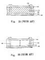
- FIG. 1illustrates a cross-sectional view of a conventional display cell.
- Every optical interference display cell 100comprises two walls, wall 102 and wall 104 .
- the wall 102 and the wall 104are supported by supporters 106 , and a cavity 108 is subsequently formed between the wall 102 , the wall 104 and the supporters 106 .
- the distance between the wall 102 and the wall 104that is, the length of the cavity 108 , is D.
- Either the wall 102 or the wall 104is a semi-transmissible/semi-reflective layer with an absorption rate that partially absorbs visible light, and the other is a light reflective layer that is deformable when voltage is applied.
- the optical interference display cell 100is “open”.
- FIG. 2illustrates a cross-sectional view of a conventional display cell after a voltage is applied.
- the wall 104is deformed and falls down towards the wall 102 due to the attraction of static electricity.
- the distance between the wall 102 and the wall 104that is, the length of the cavity 108 , is not exactly equal to zero, but is d, which can be equal to zero. If D in formula 1.1 is replaced with d, only visible light with a wavelength ⁇ 2 satisfying formula 1.1 in wavelengths ⁇ of all visible light spectra of the incident light can generate a constructive interference, be reflected by the wall 104 , and pass through the wall 102 .
- the optical interference display cell 100is now “closed”.
- FIG. 3 A and FIG. 3Billustrate a method for manufacturing a conventional display cell.
- a first electrode 110 and a sacrificial layer 111are formed in sequence on a transparent substrate 109 , and opening 112 , which is suitable for forming a supporter therein, is formed in the first electrode 110 and the sacrificial layer 111 .
- a supporter 106is formed in the opening 112 .
- an electrode 114is formed on the sacrificial layer 111 and the supporter 106 .
- the sacrificial layer 111 shown in FIG. 3Ais removed by a release etching process to form a cavity 116 , which is located in the position of the sacrificial layer 111 , and the length D of the cavity 116 is the thickness of the sacrificial layer 111 .
- a micro suspended structureis fabricated by use a sacrificial layer.
- a suspended movable microstructureis fabricated by a selective etching between a device structure layer and the sacrificial layer to remove the sacrificial layer and leave the structure layer, and this process is called a structure release etching.
- the difference between the structure release etching process and an IC processis that in the structure release etching process, the selective etching is an isotropic etching, so that an undercut or an under etching is formed in the structure layer for smooth separation of the structure layer and the substrate.
- the most popular structure release etching processis a wet structure release process.
- a rinsing step and a drying stepusually have to be performed after etching, and a microstructure can substantially be suspended above the substrate.
- a dry etching process using xenon difluoride (XeF 2 ) as an etchantcan be used to solve the problems resulted in the wet etching process.
- Xenon difluorideis in a solid state at normal temperature and normal pressure, and is sublimated into the gaseous state at low pressure.
- Xenon difluoridehas great etching selectivity on silicon materials, such as monocrystalline silicon, polysilicon and amorphous silicon, and some metals, such as molybdenum (Mo), molybdenum alloy and so on.
- silicon materialssuch as monocrystalline silicon, polysilicon and amorphous silicon
- some metalssuch as molybdenum (Mo), molybdenum alloy and so on.
- Momolybdenum
- Xenonis an inert gases, and xenon difluoride is quite unstable.
- xenon difluorideThe etching mechanism of xenon difluoride is that two fluorine free radicals are brought to the reaction positions by xenon, and when xenon difluoride contacts the material to be etched, xenon difluoride decomposes to release these two fluorine free radicals. Because the isotropic etching effect of xenon difluoride is great, xenon difluoride has an excellent capacity for lateral etching. In a micro electro mechanical system process, xenon difluoride is used as an etchant to remove a sacrificial layer in a structure release etching process.
- FIG. 4illustrates a top view of a conventional optical interference display cell.
- the optical interference display cell 200includes separation structures 202 , such as defined by dotted lines 2021 , located on two opposite sides of the optical interference display cell 200 , and supporters 204 located on the other two opposite sides of the optical interference display cell 200 .
- the separation structures 202 and the supporters 204are located between two electrodes. There are gaps between the supporters 204 , and the supporters 204 and the separation structures 202 .
- the gaseous xenon difluoridepermeates through the gaps and etches a sacrificial layer (not shown in FIG. 4 ).
- the rate of a structure release etching process with an etchant of the gaseous xenon difluoridechanges with the different materials of the sacrificial layers desired to be etched.
- the etching ratecan be greater than 10 micrometers per minute, and even can be up to 20-30 micrometers per minute for some materials.
- one structure release etching processonly takes dozens of seconds to 3 minutes.
- xenon difluorideis expensive, and is particularly sensitive to moisture and is unstable. When xenon difluoride contacts moisture, hydrogen fluoride is produced. Hydrogen fluoride is not only dangerous, but also reduces efficiency of etching.
- the structure release etching process performed using xenon difluoride as an etchantis rare in semiconductor processes and typical planar display processes, so etchers that are maturely developed in the semiconductor processes and the liquid crystal display processes are unsuitable for the structure release etching process with xenon difluoride etchant.
- the process apparatuses used in semiconductor or typical planar displaycan be continuously used in most of the main processes of the optical interference display, but the structure release etching process needs a totally different apparatus design. To reorganize and consolidate the process apparatuses would be an obstacle to the development and throughput of the optical interference display.
- etching apparatus used in typical semiconductor or planar displayis not suitable for use in the structure release etching process is the poor capacity for lateral etching, and even though an etchant with a great etching property, for example, nitrogen trifluoride (NF 3 ) or sulphur hexafluoride (SF 6 ), is used, the etching rate is only between 3 micrometers and 10 micrometers per minute. This is slower than that for using xenon difluoride as an etchant by several to dozens of times. Therefore, this is very disadvantageous to throughput of the optical interference display.
- NF 3nitrogen trifluoride
- SF 6sulphur hexafluoride
- an objective of the present inventionis to provide a structure of a structure release suitable for an optical interference display cell structure. Time needed for the structure etching process can be greatly reduced and throughput of the optical interference display can be increased.
- Another objective of the present inventionis to provide a structure of a structure release suitable for an optical interference display cell structure, in which a xenon difluoride process is not needed to perform a structure release etching, thereby avoiding the difficulties resulting from reorganizing and consolidating the process apparatuses.
- Still another objective of the present inventionis to provide a structure release etching process for a structure of a structure release suitable for an optical interference display cell structure.
- an etching reagentincluding a fluorine base or a chlorine base, such as CF 4 , BCl 3 , NF 3 , or SF 6 and so on, can be used to replace xenon difluoride to perform the structure release etching, thereby lowering producing cost.
- Yet another objective of the present inventionis to provide a structure release etching process for a structure of a structure release suitable for an optical interference display cell structure.
- the structure release etching processcan use a conventional etching apparatus, so the difficulties resulting from reorganizing and consolidating the process apparatuses can be avoided.
- An optical interference display cell structureincludes a first electrode and a second electrode, the two electrodes being supported by a supporter, which is located between the two electrodes.
- a plurality of holesare located on the second electrode, and the holes pass through the second electrode and expose a sacrificial layer under the second electrode. With the holes in the second electrode, etching plasma can etch the exposed sacrificial layer through the holes, so as to accelerate a structure release etching process.
- the etching process using an etchant including a fluorine base or a chlorine base, such as CF 4 , BCl 3 , NF 3 , or SF 6 and so on, suitable for conventional semiconductor or typical planar display processcan be used to perform a structure release etching process of the optical interference display cell, and process time of the structure release etching process is commensurate with that of xenon difluoride process.
- the etching reagents including a fluorine base or a chlorine basecan be adapted and mixed to form an etchant for etching the sacrificial layer.
- the present inventionpreferably uses remote plasma.
- a plasmais first produced in a plasma generator, and after portion or all of the charged composition in the plasma is filtered out, the remaining plasma, the remote plasma, is sent into a chamber to perform a reaction.
- Free radicalsare the main composition of the remote plasma, so a life cycle of the remote plasma is longer and the structure release etching of the sacrificial layer is performed efficiently.
- the free radicalsare not charged and not easily affected by an electric field, so the effect of isotropic etching is better for being beneficial to lateral etching.
- the holes in the second electrodecan indeed reduce the time taken in the structure release etching, to make it possible for a conventional etching process to replace a xenon difluoride etching process, and to avoid the difficulties resulting from reorganizing and consolidating the process apparatuses.
- the use of the remote plasmaincreases the lift cycle of the etching plasma and the lateral etching capacity of the plasma, accelerates the rate of the structure release etching, decrease the time needed in the structure release etching, and increases the throughput of the optical interference display.
- FIG. 1illustrates a cross-sectional view of a conventional display cell
- FIG. 2illustrates a cross-sectional view of a conventional display cell after a voltage is applied
- FIG. 3 A and FIG. 3Billustrate a method for manufacturing a conventional display cell
- FIG. 4illustrates a top view of a conventional optical interference display cell
- FIG. 4Aillustrates a cross-sectional view of the structure shown in FIG. 4 along cross-sectional line I-I′;
- FIG. 5illustrates a top view of an optical interference display cell in accordance with a preferred embodiment of the present invention
- FIG. 5Aillustrates an enlargement of a cross-sectional view of a circle 308 shown in FIG. 5 along cross-sectional line II-II′;
- FIG. 6A to FIG. 6Cillustrate a method for manufacturing an optical interference display cell structure in accordance with a preferred embodiment of the present invention.
- an embodiment of the present invention hereintakes an optical interference display cell structure and a manufacturing method thereof for example, to illustrate how to apply the structure of the structure release and the method for manufacturing the same disclosed in the present invention, and to further explain advantages of the present invention according to the disclosure of the embodiment.
- FIG. 5illustrates a top view of an optical interference display cell in accordance with a preferred embodiment of the present invention.
- an optical interference display cell 300includes an electrode 301 , separation structures 302 , such as defined by a dotted line 3021 , and supporters 304 .
- the separation structures 302are located on two opposite sides of the optical interference display cell 300 .
- the supporters 304are located on another two opposite sides of the optical interference display cell 300 , and the separation structures 302 and the supporters 304 are located between the electrode 301 and another electrode (not shown in FIG. 5 ).
- the electrode 301includes at least one hole 306 , which passes through the electrode 301 .
- the diameter of the hole 306is preferably not less than 1 micrometer. As the diameter of the hole 306 increases, the etching time decreases, but the larger hole 306 is not beneficial to the resolution of the optical interference display cell 300 . Therefore, the diameter of the hole 306 is preferably not greater than 10 micrometers. In conclusion, a preferred diameter of the hole 306 is between about 1 micrometer and 5 micrometers. There are gaps between the supporters 304 , and between each of the supporters 304 and the separation structures 302 , and etching plasma can permeate through the gaps and the hole 306 and etch a sacrificial layer (not shown in FIG. 5 ).
- the size of the optical interference display cell 300is between about 50 micrometers and 100 micrometers.
- FIG. 4Aillustrates a cross-sectional view of the structure shown in FIG. 4 along cross-sectional line I-I′.
- the gaseous xenon difluoridepermeates through gaps 208 between the supporters (not shown in FIG. 4 A), and between the supporters and the separation structures (not shown in FIG. 4A ) to etch the sacrificial layer 210 toward the directions indicated by arrowheads 206 .
- FIG. 5Aillustrates an enlargement of a cross-sectional view of a circle 308 shown in FIG. 5 along cross-sectional line II-II′.
- a fluorine base or a chlorine basesuch as CF 4 , BCl 3 , NF 3 , or SF 6
- the etching plasmanot only permeates through gaps 312 between the supporters (not shown in FIG. 5 A), and between the supporters and the separation structures (not shown in FIG.
- optical interference display cell structure disclosed in the present inventionenables the introduction of the conventional etching process, so the xenon difluoride etching process, which is expensive and not easy to reorganize and consolidate, is not needed, thereby avoiding the difficulties resulting from reorganizing and consolidating the process apparatuses.
- FIG. 6A to FIG. 6Cillustrate a method for manufacturing an optical interference display cell structure in accordance with a preferred embodiment of the present invention.
- a first electrode 402 and a sacrificial layer 406are firmed on a transparent substrate 401 in sequence.
- the material of the sacrificial layer 406can be transparent material, such as dielectric material, or opaque material, such as metal material, polysilicon or amorphous silicon.
- polysiliconis used as the material of the sacrificial layer 406 .
- An opening 408is formed in the first electrode 402 and the sacrificial layer 406 by a photolithography process, and the opening 408 is suitable for forming a supporter therein.
- a material layer 410is formed on the sacrificial layer 406 to fill up the opening 408 .
- the material layer 410is suitable for forming the supporter, and the first material layer 410 generally is made of photosensitive materials such as photoresists, or a non-photosensitive polymer materials such as polyester, polyamide or the like. If non-photosensitive materials are used for forming the material layer 410 , a photolithographic etching process is required to define supporters in the material layer 410 . In this embodiment, the photosensitive materials are used for forming the material layer 410 , so merely a photolithography process is required for patterning the material layer 410 .
- supporters 412are defined by patterning the material layer 410 through a photolithography process.
- a second electrode 404is formed on the sacrificial layer 406 and the supporters 412 .
- the second electrode 404includes at least one hole 414 .
- remote plasmais produced by using an etching reagent including a fluorine base or a chlorine base, such as CF 4 , BCl 3 , NF 3 , or SF 6 and so on, as a precursor to etch the sacrificial layer 406 .
- the remote plasmaetches the sacrificial layer 406 not only through the gaps (not shown in FIG. 6B ) between the supporters, but also through the hole 414 , so the sacrificial layer 406 is removed by a structure release etching process, and a cavity 416 such as illustrated in FIG. 6C is formed.
- the materials suitable for forming the supporters 412include positive photoresists, negative photoresists, and all kinds of polymers, such as acrylic resins and epoxy resins.
- the number of holesrelates to the size of the optical interference display cell and the size of the hole.
- the size of the optical interference display cellis between about 50 micrometers and 100 micrometers, and the diameter of a hole is between 1 micrometer and 5 micrometers, 4 to 16 holes are needed to shorter time taken in a structure release etching process to an acceptable level.
- the size of the optical interference display cellis less than 50 micrometers, the number of the holes may be less than 4, and even only one hole is needed to shorter time taken in a structure release etching process to an acceptable level.
- the hole in the deformable electrodecan substantially reduce time of a structure release etching process, so that etching processes suitable for semiconductor or planar display processes can be applied in the structure release etching process of the optical interference display cell structure, thereby avoiding the difficulties resulting from reorganizing and consolidating the xenon difluoride etching process apparatuses and the other deposition process apparatuses. Furthermore, fabrication cost can be reduced because the expensive xenon difluoride etching process is not needed.
Landscapes
- Physics & Mathematics (AREA)
- General Physics & Mathematics (AREA)
- Optics & Photonics (AREA)
- Spectroscopy & Molecular Physics (AREA)
- Micromachines (AREA)
- Mechanical Light Control Or Optical Switches (AREA)
Abstract
Description
2D=Nλ (1.1)
where N is a natural number.
Claims (17)
Applications Claiming Priority (2)
| Application Number | Priority Date | Filing Date | Title |
|---|---|---|---|
| TW92114190 | 2003-05-26 | ||
| TW092114190ATW591716B (en) | 2003-05-26 | 2003-05-26 | A structure of a structure release and manufacturing the same |
Publications (2)
| Publication Number | Publication Date |
|---|---|
| US20040240027A1 US20040240027A1 (en) | 2004-12-02 |
| US6870654B2true US6870654B2 (en) | 2005-03-22 |
Family
ID=33448904
Family Applications (1)
| Application Number | Title | Priority Date | Filing Date |
|---|---|---|---|
| US10/725,585Expired - Fee RelatedUS6870654B2 (en) | 2003-05-26 | 2003-12-03 | Structure of a structure release and a method for manufacturing the same |
Country Status (4)
| Country | Link |
|---|---|
| US (1) | US6870654B2 (en) |
| JP (1) | JP2004351607A (en) |
| KR (1) | KR100623565B1 (en) |
| TW (1) | TW591716B (en) |
Cited By (159)
| Publication number | Priority date | Publication date | Assignee | Title |
|---|---|---|---|---|
| US20020075555A1 (en)* | 1994-05-05 | 2002-06-20 | Iridigm Display Corporation | Interferometric modulation of radiation |
| US20040209192A1 (en)* | 2003-04-21 | 2004-10-21 | Prime View International Co., Ltd. | Method for fabricating an interference display unit |
| US20050003667A1 (en)* | 2003-05-26 | 2005-01-06 | Prime View International Co., Ltd. | Method for fabricating optical interference display cell |
| US20050046948A1 (en)* | 2003-08-26 | 2005-03-03 | Wen-Jian Lin | Interference display cell and fabrication method thereof |
| US20050078348A1 (en)* | 2003-09-30 | 2005-04-14 | Wen-Jian Lin | Structure of a micro electro mechanical system and the manufacturing method thereof |
| US20050122560A1 (en)* | 2003-12-09 | 2005-06-09 | Sampsell Jeffrey B. | Area array modulation and lead reduction in interferometric modulators |
| US20050142684A1 (en)* | 2002-02-12 | 2005-06-30 | Miles Mark W. | Method for fabricating a structure for a microelectromechanical system (MEMS) device |
| US20060001942A1 (en)* | 2004-07-02 | 2006-01-05 | Clarence Chui | Interferometric modulators with thin film transistors |
| US20060066856A1 (en)* | 2004-09-27 | 2006-03-30 | William Cummings | Systems and methods for measuring color and contrast in specular reflective devices |
| US20060066864A1 (en)* | 2004-09-27 | 2006-03-30 | William Cummings | Process control monitors for interferometric modulators |
| US20060066595A1 (en)* | 2004-09-27 | 2006-03-30 | Sampsell Jeffrey B | Method and system for driving a bi-stable display |
| US20060066504A1 (en)* | 2004-09-27 | 2006-03-30 | Sampsell Jeffrey B | System with server based control of client device display features |
| US20060066936A1 (en)* | 2004-09-27 | 2006-03-30 | Clarence Chui | Interferometric optical modulator using filler material and method |
| US20060066596A1 (en)* | 2004-09-27 | 2006-03-30 | Sampsell Jeffrey B | System and method of transmitting video data |
| US20060067643A1 (en)* | 2004-09-27 | 2006-03-30 | Clarence Chui | System and method for multi-level brightness in interferometric modulation |
| US20060066876A1 (en)* | 2004-09-27 | 2006-03-30 | Manish Kothari | Method and system for sensing light using interferometric elements |
| US20060065043A1 (en)* | 2004-09-27 | 2006-03-30 | William Cummings | Method and system for detecting leak in electronic devices |
| US20060066543A1 (en)* | 2004-09-27 | 2006-03-30 | Gally Brian J | Ornamental display device |
| US20060066863A1 (en)* | 2004-09-27 | 2006-03-30 | Cummings William J | Electro-optical measurement of hysteresis in interferometric modulators |
| US20060067652A1 (en)* | 2004-09-27 | 2006-03-30 | Cummings William J | Methods for visually inspecting interferometric modulators for defects |
| US20060066932A1 (en)* | 2004-09-27 | 2006-03-30 | Clarence Chui | Method of selective etching using etch stop layer |
| US20060077527A1 (en)* | 2004-09-27 | 2006-04-13 | Cummings William J | Methods and devices for inhibiting tilting of a mirror in an interferometric modulator |
| US20060077393A1 (en)* | 2004-09-27 | 2006-04-13 | Gally Brian J | System and method for implementation of interferometric modulator displays |
| US20060077523A1 (en)* | 2004-09-27 | 2006-04-13 | Cummings William J | Electrical characterization of interferometric modulators |
| US20060077510A1 (en)* | 2004-09-27 | 2006-04-13 | Clarence Chui | System and method of illuminating interferometric modulators using backlighting |
| US20060077617A1 (en)* | 2004-09-27 | 2006-04-13 | Floyd Philip D | Selectable capacitance circuit |
| US20060077507A1 (en)* | 2004-09-27 | 2006-04-13 | Clarence Chui | Conductive bus structure for interferometric modulator array |
| US20060077521A1 (en)* | 2004-09-27 | 2006-04-13 | Gally Brian J | System and method of implementation of interferometric modulators for display mirrors |
| US20060077508A1 (en)* | 2004-09-27 | 2006-04-13 | Clarence Chui | Method and device for multistate interferometric light modulation |
| US20060103643A1 (en)* | 2004-09-27 | 2006-05-18 | Mithran Mathew | Measuring and modeling power consumption in displays |
| US20060187523A1 (en)* | 2003-10-27 | 2006-08-24 | Pan Shaoher X | Fabricating micro devices using sacrificial materials |
| US7138984B1 (en) | 2001-06-05 | 2006-11-21 | Idc, Llc | Directly laminated touch sensitive screen |
| US20060277486A1 (en)* | 2005-06-02 | 2006-12-07 | Skinner David N | File or user interface element marking system |
| US7161730B2 (en) | 2004-09-27 | 2007-01-09 | Idc, Llc | System and method for providing thermal compensation for an interferometric modulator display |
| US7172915B2 (en) | 2003-01-29 | 2007-02-06 | Qualcomm Mems Technologies Co., Ltd. | Optical-interference type display panel and method for making the same |
| US7236284B2 (en) | 1995-05-01 | 2007-06-26 | Idc, Llc | Photonic MEMS and structures |
| US20070177129A1 (en)* | 2006-01-06 | 2007-08-02 | Manish Kothari | System and method for providing residual stress test structures |
| US20070194414A1 (en)* | 2006-02-21 | 2007-08-23 | Chen-Jean Chou | Method for providing and removing discharging interconnect for chip-on-glass output leads and structures thereof |
| US20070242008A1 (en)* | 2006-04-17 | 2007-10-18 | William Cummings | Mode indicator for interferometric modulator displays |
| US20070249081A1 (en)* | 2006-04-19 | 2007-10-25 | Qi Luo | Non-planar surface structures and process for microelectromechanical systems |
| US7297471B1 (en) | 2003-04-15 | 2007-11-20 | Idc, Llc | Method for manufacturing an array of interferometric modulators |
| US7304784B2 (en) | 2004-09-27 | 2007-12-04 | Idc, Llc | Reflective display device having viewable display on both sides |
| US20070290961A1 (en)* | 2006-06-15 | 2007-12-20 | Sampsell Jeffrey B | Method and apparatus for low range bit depth enhancement for MEMS display architectures |
| US20080002210A1 (en)* | 2006-06-30 | 2008-01-03 | Kostadin Djordjev | Determination of interferometric modulator mirror curvature and airgap variation using digital photographs |
| US20080013144A1 (en)* | 2004-09-27 | 2008-01-17 | Idc, Llc | Microelectromechanical device with optical function separated from mechanical and electrical function |
| US20080013145A1 (en)* | 2004-09-27 | 2008-01-17 | Idc, Llc | Microelectromechanical device with optical function separated from mechanical and electrical function |
| US7321457B2 (en) | 2006-06-01 | 2008-01-22 | Qualcomm Incorporated | Process and structure for fabrication of MEMS device having isolated edge posts |
| US7321456B2 (en) | 2004-09-27 | 2008-01-22 | Idc, Llc | Method and device for corner interferometric modulation |
| US7327510B2 (en) | 2004-09-27 | 2008-02-05 | Idc, Llc | Process for modifying offset voltage characteristics of an interferometric modulator |
| US20080030825A1 (en)* | 2006-04-19 | 2008-02-07 | Qualcomm Incorporated | Microelectromechanical device and method utilizing a porous surface |
| US7343080B2 (en) | 2004-09-27 | 2008-03-11 | Idc, Llc | System and method of testing humidity in a sealed MEMS device |
| US7349136B2 (en) | 2004-09-27 | 2008-03-25 | Idc, Llc | Method and device for a display having transparent components integrated therein |
| US20080094690A1 (en)* | 2006-10-18 | 2008-04-24 | Qi Luo | Spatial Light Modulator |
| US7369296B2 (en) | 2004-09-27 | 2008-05-06 | Idc, Llc | Device and method for modifying actuation voltage thresholds of a deformable membrane in an interferometric modulator |
| US7369292B2 (en) | 2006-05-03 | 2008-05-06 | Qualcomm Mems Technologies, Inc. | Electrode and interconnect materials for MEMS devices |
| US7373026B2 (en) | 2004-09-27 | 2008-05-13 | Idc, Llc | MEMS device fabricated on a pre-patterned substrate |
| US7372619B2 (en) | 1994-05-05 | 2008-05-13 | Idc, Llc | Display device having a movable structure for modulating light and method thereof |
| US7382515B2 (en) | 2006-01-18 | 2008-06-03 | Qualcomm Mems Technologies, Inc. | Silicon-rich silicon nitrides as etch stops in MEMS manufacture |
| US7385744B2 (en) | 2006-06-28 | 2008-06-10 | Qualcomm Mems Technologies, Inc. | Support structure for free-standing MEMS device and methods for forming the same |
| US7405863B2 (en) | 2006-06-01 | 2008-07-29 | Qualcomm Mems Technologies, Inc. | Patterning of mechanical layer in MEMS to reduce stresses at supports |
| US7405861B2 (en) | 2004-09-27 | 2008-07-29 | Idc, Llc | Method and device for protecting interferometric modulators from electrostatic discharge |
| US20080186581A1 (en)* | 2007-02-01 | 2008-08-07 | Qualcomm Incorporated | Modulating the intensity of light from an interferometric reflector |
| US7417783B2 (en) | 2004-09-27 | 2008-08-26 | Idc, Llc | Mirror and mirror layer for optical modulator and method |
| US7420725B2 (en) | 2004-09-27 | 2008-09-02 | Idc, Llc | Device having a conductive light absorbing mask and method for fabricating same |
| US7420728B2 (en) | 2004-09-27 | 2008-09-02 | Idc, Llc | Methods of fabricating interferometric modulators by selectively removing a material |
| US20080231931A1 (en)* | 2007-03-21 | 2008-09-25 | Qualcomm Incorporated | Mems cavity-coating layers and methods |
| US20080239455A1 (en)* | 2007-03-28 | 2008-10-02 | Lior Kogut | Microelectromechanical device and method utilizing conducting layers separated by stops |
| US7446926B2 (en) | 2004-09-27 | 2008-11-04 | Idc, Llc | System and method of providing a regenerating protective coating in a MEMS device |
| US7450295B2 (en) | 2006-03-02 | 2008-11-11 | Qualcomm Mems Technologies, Inc. | Methods for producing MEMS with protective coatings using multi-component sacrificial layers |
| US20080278787A1 (en)* | 2007-05-09 | 2008-11-13 | Qualcomm Incorporated | Microelectromechanical system having a dielectric movable membrane and a mirror |
| US20080278788A1 (en)* | 2007-05-09 | 2008-11-13 | Qualcomm Incorporated | Microelectromechanical system having a dielectric movable membrane and a mirror |
| US7453579B2 (en) | 2004-09-27 | 2008-11-18 | Idc, Llc | Measurement of the dynamic characteristics of interferometric modulators |
| US7460292B2 (en) | 2005-06-03 | 2008-12-02 | Qualcomm Mems Technologies, Inc. | Interferometric modulator with internal polarization and drive method |
| US20080318344A1 (en)* | 2007-06-22 | 2008-12-25 | Qualcomm Incorporated | INDICATION OF THE END-POINT REACTION BETWEEN XeF2 AND MOLYBDENUM |
| US20080316566A1 (en)* | 2007-06-19 | 2008-12-25 | Qualcomm Incorporated | High aperture-ratio top-reflective am-imod displays |
| US20080316568A1 (en)* | 2007-06-21 | 2008-12-25 | Qualcomm Incorporated | Infrared and dual mode displays |
| US20090009845A1 (en)* | 2007-07-02 | 2009-01-08 | Qualcomm Incorporated | Microelectromechanical device with optical function separated from mechanical and electrical function |
| US7476327B2 (en) | 2004-05-04 | 2009-01-13 | Idc, Llc | Method of manufacture for microelectromechanical devices |
| US20090022884A1 (en)* | 2004-07-29 | 2009-01-22 | Idc,Llc | System and method for micro-electromechanical operation of an interferometric modulator |
| US7492502B2 (en) | 2004-09-27 | 2009-02-17 | Idc, Llc | Method of fabricating a free-standing microstructure |
| US20090059346A1 (en)* | 2007-08-29 | 2009-03-05 | Qualcomm Incorporated | Interferometric Optical Modulator With Broadband Reflection Characteristics |
| US20090073539A1 (en)* | 2007-09-14 | 2009-03-19 | Qualcomm Incorporated | Periodic dimple array |
| US20090073534A1 (en)* | 2007-09-14 | 2009-03-19 | Donovan Lee | Interferometric modulator display devices |
| US20090103166A1 (en)* | 2007-10-23 | 2009-04-23 | Qualcomm Mems Technologies, Inc. | Adjustably transmissive mems-based devices |
| US20090101192A1 (en)* | 2007-10-19 | 2009-04-23 | Qualcomm Incorporated | Photovoltaic devices with integrated color interferometric film stacks |
| US7527998B2 (en) | 2006-06-30 | 2009-05-05 | Qualcomm Mems Technologies, Inc. | Method of manufacturing MEMS devices providing air gap control |
| US7527995B2 (en) | 2004-09-27 | 2009-05-05 | Qualcomm Mems Technologies, Inc. | Method of making prestructure for MEMS systems |
| US7532377B2 (en) | 1998-04-08 | 2009-05-12 | Idc, Llc | Movable micro-electromechanical device |
| US7534640B2 (en) | 2005-07-22 | 2009-05-19 | Qualcomm Mems Technologies, Inc. | Support structure for MEMS device and methods therefor |
| US20090126777A1 (en)* | 2007-11-16 | 2009-05-21 | Qualcomm Mems Technologies, Inc. | Simultaneous light collection and illumination on an active display |
| US20090147343A1 (en)* | 2007-12-07 | 2009-06-11 | Lior Kogut | Mems devices requiring no mechanical support |
| US7547568B2 (en) | 2006-02-22 | 2009-06-16 | Qualcomm Mems Technologies, Inc. | Electrical conditioning of MEMS device and insulating layer thereof |
| US7547565B2 (en) | 2005-02-04 | 2009-06-16 | Qualcomm Mems Technologies, Inc. | Method of manufacturing optical interference color display |
| US7550810B2 (en) | 2006-02-23 | 2009-06-23 | Qualcomm Mems Technologies, Inc. | MEMS device having a layer movable at asymmetric rates |
| US7550794B2 (en) | 2002-09-20 | 2009-06-23 | Idc, Llc | Micromechanical systems device comprising a displaceable electrode and a charge-trapping layer |
| US20090159123A1 (en)* | 2007-12-21 | 2009-06-25 | Qualcomm Mems Technologies, Inc. | Multijunction photovoltaic cells |
| US7554711B2 (en) | 1998-04-08 | 2009-06-30 | Idc, Llc. | MEMS devices with stiction bumps |
| US7553684B2 (en) | 2004-09-27 | 2009-06-30 | Idc, Llc | Method of fabricating interferometric devices using lift-off processing techniques |
| US7554714B2 (en) | 2004-09-27 | 2009-06-30 | Idc, Llc | Device and method for manipulation of thermal response in a modulator |
| US7564612B2 (en) | 2004-09-27 | 2009-07-21 | Idc, Llc | Photonic MEMS and structures |
| US7566664B2 (en) | 2006-08-02 | 2009-07-28 | Qualcomm Mems Technologies, Inc. | Selective etching of MEMS using gaseous halides and reactive co-etchants |
| US7586484B2 (en) | 2004-09-27 | 2009-09-08 | Idc, Llc | Controller and driver features for bi-stable display |
| US20090225395A1 (en)* | 2008-03-07 | 2009-09-10 | Qualcomm Mems Technologies, Inc. | Interferometric modulator in transmission mode |
| US20090251761A1 (en)* | 2008-04-02 | 2009-10-08 | Kasra Khazeni | Microelectromechanical systems display element with photovoltaic structure |
| US20090257105A1 (en)* | 2008-04-10 | 2009-10-15 | Qualcomm Mems Technologies, Inc. | Device having thin black mask and method of fabricating the same |
| US7612933B2 (en) | 2008-03-27 | 2009-11-03 | Qualcomm Mems Technologies, Inc. | Microelectromechanical device with spacing layer |
| US7616369B2 (en) | 2003-06-24 | 2009-11-10 | Idc, Llc | Film stack for manufacturing micro-electromechanical systems (MEMS) devices |
| US7623287B2 (en) | 2006-04-19 | 2009-11-24 | Qualcomm Mems Technologies, Inc. | Non-planar surface structures and process for microelectromechanical systems |
| US20090293955A1 (en)* | 2007-11-07 | 2009-12-03 | Qualcomm Incorporated | Photovoltaics with interferometric masks |
| US7630119B2 (en) | 2004-09-27 | 2009-12-08 | Qualcomm Mems Technologies, Inc. | Apparatus and method for reducing slippage between structures in an interferometric modulator |
| US7630114B2 (en) | 2005-10-28 | 2009-12-08 | Idc, Llc | Diffusion barrier layer for MEMS devices |
| US20090323153A1 (en)* | 2008-06-25 | 2009-12-31 | Qualcomm Mems Technologies, Inc. | Backlight displays |
| US20090323165A1 (en)* | 2008-06-25 | 2009-12-31 | Qualcomm Mems Technologies, Inc. | Method for packaging a display device and the device obtained thereof |
| US7643203B2 (en) | 2006-04-10 | 2010-01-05 | Qualcomm Mems Technologies, Inc. | Interferometric optical display system with broadband characteristics |
| US7649671B2 (en) | 2006-06-01 | 2010-01-19 | Qualcomm Mems Technologies, Inc. | Analog interferometric modulator device with electrostatic actuation and release |
| US20100022095A1 (en)* | 2005-11-22 | 2010-01-28 | Air Products And Chemicals, Inc. | Selective Etching and Formation of Xenon Difluoride |
| US20100053148A1 (en)* | 2008-09-02 | 2010-03-04 | Qualcomm Mems Technologies, Inc. | Light turning device with prismatic light turning features |
| US20100096011A1 (en)* | 2008-10-16 | 2010-04-22 | Qualcomm Mems Technologies, Inc. | High efficiency interferometric color filters for photovoltaic modules |
| US7706050B2 (en) | 2004-03-05 | 2010-04-27 | Qualcomm Mems Technologies, Inc. | Integrated modulator illumination |
| US7711239B2 (en) | 2006-04-19 | 2010-05-04 | Qualcomm Mems Technologies, Inc. | Microelectromechanical device and method utilizing nanoparticles |
| US7719500B2 (en) | 2004-09-27 | 2010-05-18 | Qualcomm Mems Technologies, Inc. | Reflective display pixels arranged in non-rectangular arrays |
| US7719752B2 (en) | 2007-05-11 | 2010-05-18 | Qualcomm Mems Technologies, Inc. | MEMS structures, methods of fabricating MEMS components on separate substrates and assembly of same |
| US20100128337A1 (en)* | 2008-07-11 | 2010-05-27 | Yeh-Jiun Tung | Stiction mitigation with integrated mech micro-cantilevers through vertical stress gradient control |
| US20100147790A1 (en)* | 2005-07-22 | 2010-06-17 | Qualcomm Mems Technologies, Inc. | Support structure for mems device and methods therefor |
| US7763546B2 (en) | 2006-08-02 | 2010-07-27 | Qualcomm Mems Technologies, Inc. | Methods for reducing surface charges during the manufacture of microelectromechanical systems devices |
| US7768690B2 (en) | 2008-06-25 | 2010-08-03 | Qualcomm Mems Technologies, Inc. | Backlight displays |
| US20100202039A1 (en)* | 2005-08-19 | 2010-08-12 | Qualcomm Mems Technologies, Inc. | Mems devices having support structures with substantially vertical sidewalls and methods for fabricating the same |
| US7781850B2 (en) | 2002-09-20 | 2010-08-24 | Qualcomm Mems Technologies, Inc. | Controlling electromechanical behavior of structures within a microelectromechanical systems device |
| US7795061B2 (en) | 2005-12-29 | 2010-09-14 | Qualcomm Mems Technologies, Inc. | Method of creating MEMS device cavities by a non-etching process |
| US20100238572A1 (en)* | 2009-03-23 | 2010-09-23 | Qualcomm Mems Technologies, Inc. | Display device with openings between sub-pixels and method of making same |
| US20100236624A1 (en)* | 2007-09-24 | 2010-09-23 | Qualcomm Mems Technologies, Inc. | Interferometric photovoltaic cell |
| US20100245977A1 (en)* | 2009-03-27 | 2010-09-30 | Qualcomm Mems Technologies, Inc. | Post-release adjustment of interferometric modulator reflectivity |
| US7813026B2 (en) | 2004-09-27 | 2010-10-12 | Qualcomm Mems Technologies, Inc. | System and method of reducing color shift in a display |
| US20100284055A1 (en)* | 2007-10-19 | 2010-11-11 | Qualcomm Mems Technologies, Inc. | Display with integrated photovoltaic device |
| US7835061B2 (en) | 2006-06-28 | 2010-11-16 | Qualcomm Mems Technologies, Inc. | Support structures for free-standing electromechanical devices |
| US7855826B2 (en) | 2008-08-12 | 2010-12-21 | Qualcomm Mems Technologies, Inc. | Method and apparatus to reduce or eliminate stiction and image retention in interferometric modulator devices |
| US20110026095A1 (en)* | 2007-07-31 | 2011-02-03 | Qualcomm Mems Technologies, Inc. | Devices and methods for enhancing color shift of interferometric modulators |
| US7884989B2 (en) | 2005-05-27 | 2011-02-08 | Qualcomm Mems Technologies, Inc. | White interferometric modulators and methods for forming the same |
| US7893919B2 (en) | 2004-09-27 | 2011-02-22 | Qualcomm Mems Technologies, Inc. | Display region architectures |
| US20110063712A1 (en)* | 2009-09-17 | 2011-03-17 | Qualcomm Mems Technologies, Inc. | Display device with at least one movable stop element |
| US7916980B2 (en) | 2006-01-13 | 2011-03-29 | Qualcomm Mems Technologies, Inc. | Interconnect structure for MEMS device |
| US20110075241A1 (en)* | 2009-09-28 | 2011-03-31 | Qualcomm Mems Technologies, Inc. | Interferometric display with interferometric reflector |
| US7936497B2 (en) | 2004-09-27 | 2011-05-03 | Qualcomm Mems Technologies, Inc. | MEMS device having deformable membrane characterized by mechanical persistence |
| US8008736B2 (en) | 2004-09-27 | 2011-08-30 | Qualcomm Mems Technologies, Inc. | Analog interferometric modulator device |
| US8059326B2 (en) | 1994-05-05 | 2011-11-15 | Qualcomm Mems Technologies Inc. | Display devices comprising of interferometric modulator and sensor |
| US8164821B2 (en) | 2008-02-22 | 2012-04-24 | Qualcomm Mems Technologies, Inc. | Microelectromechanical device with thermal expansion balancing layer or stiffening layer |
| US8358458B2 (en) | 2008-06-05 | 2013-01-22 | Qualcomm Mems Technologies, Inc. | Low temperature amorphous silicon sacrificial layer for controlled adhesion in MEMS devices |
| CN101808933B (en)* | 2007-09-28 | 2013-05-01 | 高通Mems科技公司 | Multicomponent sacrificial structure |
| US8659816B2 (en) | 2011-04-25 | 2014-02-25 | Qualcomm Mems Technologies, Inc. | Mechanical layer and methods of making the same |
| US8736939B2 (en) | 2011-11-04 | 2014-05-27 | Qualcomm Mems Technologies, Inc. | Matching layer thin-films for an electromechanical systems reflective display device |
| US8797632B2 (en) | 2010-08-17 | 2014-08-05 | Qualcomm Mems Technologies, Inc. | Actuation and calibration of charge neutral electrode of a display device |
| US8817357B2 (en) | 2010-04-09 | 2014-08-26 | Qualcomm Mems Technologies, Inc. | Mechanical layer and methods of forming the same |
| US8885244B2 (en) | 2004-09-27 | 2014-11-11 | Qualcomm Mems Technologies, Inc. | Display device |
| US8928967B2 (en) | 1998-04-08 | 2015-01-06 | Qualcomm Mems Technologies, Inc. | Method and device for modulating light |
| US8963159B2 (en) | 2011-04-04 | 2015-02-24 | Qualcomm Mems Technologies, Inc. | Pixel via and methods of forming the same |
| US8979349B2 (en) | 2009-05-29 | 2015-03-17 | Qualcomm Mems Technologies, Inc. | Illumination devices and methods of fabrication thereof |
| US9057872B2 (en) | 2010-08-31 | 2015-06-16 | Qualcomm Mems Technologies, Inc. | Dielectric enhanced mirror for IMOD display |
| US9134527B2 (en) | 2011-04-04 | 2015-09-15 | Qualcomm Mems Technologies, Inc. | Pixel via and methods of forming the same |
| US9244302B2 (en) | 2013-01-16 | 2016-01-26 | Samsung Display Co., Ltd. | Display device and a method of manufacturing the same |
Families Citing this family (4)
| Publication number | Priority date | Publication date | Assignee | Title |
|---|---|---|---|---|
| KR101375337B1 (en) | 2005-07-22 | 2014-03-18 | 퀄컴 엠이엠에스 테크놀로지스, 인크. | Electomechanical devices having support structures and methods of fabricating the same |
| WO2007043383A1 (en)* | 2005-10-07 | 2007-04-19 | Nikon Corporation | Fine structure body and method for manufacturing same |
| TWI444323B (en) | 2010-02-03 | 2014-07-11 | Prime View Int Co Ltd | Driving memberand driving member array module |
| KR101989790B1 (en)* | 2012-06-08 | 2019-06-18 | 삼성디스플레이 주식회사 | Display panel, display apparatus having the same and method of manufacturing the same |
Citations (3)
| Publication number | Priority date | Publication date | Assignee | Title |
|---|---|---|---|---|
| US5835255A (en) | 1986-04-23 | 1998-11-10 | Etalon, Inc. | Visible spectrum modulator arrays |
| US20030232203A1 (en)* | 2002-01-18 | 2003-12-18 | The Regents Of The University Of Michigan | Porous polymers: compositions and uses thereof |
| US6812480B2 (en)* | 2002-01-22 | 2004-11-02 | Samsung Sdi Co., Ltd. | Triode structure field emission display device using carbon nanotubes and method of fabricating the same |
- 2003
- 2003-05-26TWTW092114190Apatent/TW591716B/ennot_activeIP Right Cessation
- 2003-12-03USUS10/725,585patent/US6870654B2/ennot_activeExpired - Fee Related
- 2003-12-11KRKR1020030090023Apatent/KR100623565B1/ennot_activeExpired - Fee Related
- 2004
- 2004-01-09JPJP2004004236Apatent/JP2004351607A/enactivePending
Patent Citations (3)
| Publication number | Priority date | Publication date | Assignee | Title |
|---|---|---|---|---|
| US5835255A (en) | 1986-04-23 | 1998-11-10 | Etalon, Inc. | Visible spectrum modulator arrays |
| US20030232203A1 (en)* | 2002-01-18 | 2003-12-18 | The Regents Of The University Of Michigan | Porous polymers: compositions and uses thereof |
| US6812480B2 (en)* | 2002-01-22 | 2004-11-02 | Samsung Sdi Co., Ltd. | Triode structure field emission display device using carbon nanotubes and method of fabricating the same |
Cited By (327)
| Publication number | Priority date | Publication date | Assignee | Title |
|---|---|---|---|---|
| US20020075555A1 (en)* | 1994-05-05 | 2002-06-20 | Iridigm Display Corporation | Interferometric modulation of radiation |
| US7372619B2 (en) | 1994-05-05 | 2008-05-13 | Idc, Llc | Display device having a movable structure for modulating light and method thereof |
| US8059326B2 (en) | 1994-05-05 | 2011-11-15 | Qualcomm Mems Technologies Inc. | Display devices comprising of interferometric modulator and sensor |
| US7236284B2 (en) | 1995-05-01 | 2007-06-26 | Idc, Llc | Photonic MEMS and structures |
| US7554711B2 (en) | 1998-04-08 | 2009-06-30 | Idc, Llc. | MEMS devices with stiction bumps |
| US9110289B2 (en) | 1998-04-08 | 2015-08-18 | Qualcomm Mems Technologies, Inc. | Device for modulating light with multiple electrodes |
| US8928967B2 (en) | 1998-04-08 | 2015-01-06 | Qualcomm Mems Technologies, Inc. | Method and device for modulating light |
| US7532377B2 (en) | 1998-04-08 | 2009-05-12 | Idc, Llc | Movable micro-electromechanical device |
| US7830586B2 (en) | 1999-10-05 | 2010-11-09 | Qualcomm Mems Technologies, Inc. | Transparent thin films |
| US7138984B1 (en) | 2001-06-05 | 2006-11-21 | Idc, Llc | Directly laminated touch sensitive screen |
| US7250315B2 (en) | 2002-02-12 | 2007-07-31 | Idc, Llc | Method for fabricating a structure for a microelectromechanical system (MEMS) device |
| US20050142684A1 (en)* | 2002-02-12 | 2005-06-30 | Miles Mark W. | Method for fabricating a structure for a microelectromechanical system (MEMS) device |
| US7642110B2 (en) | 2002-02-12 | 2010-01-05 | Qualcomm Mems Technologies, Inc. | Method for fabricating a structure for a microelectromechanical systems (MEMS) device |
| US7781850B2 (en) | 2002-09-20 | 2010-08-24 | Qualcomm Mems Technologies, Inc. | Controlling electromechanical behavior of structures within a microelectromechanical systems device |
| US7550794B2 (en) | 2002-09-20 | 2009-06-23 | Idc, Llc | Micromechanical systems device comprising a displaceable electrode and a charge-trapping layer |
| US8368124B2 (en) | 2002-09-20 | 2013-02-05 | Qualcomm Mems Technologies, Inc. | Electromechanical devices having etch barrier layers |
| US20090323168A1 (en)* | 2002-09-20 | 2009-12-31 | Idc, Llc | Electromechanical devices and methods of fabricating same |
| US7172915B2 (en) | 2003-01-29 | 2007-02-06 | Qualcomm Mems Technologies Co., Ltd. | Optical-interference type display panel and method for making the same |
| US7297471B1 (en) | 2003-04-15 | 2007-11-20 | Idc, Llc | Method for manufacturing an array of interferometric modulators |
| US7198973B2 (en) | 2003-04-21 | 2007-04-03 | Qualcomm Mems Technologies, Inc. | Method for fabricating an interference display unit |
| US20040209192A1 (en)* | 2003-04-21 | 2004-10-21 | Prime View International Co., Ltd. | Method for fabricating an interference display unit |
| US7706044B2 (en) | 2003-05-26 | 2010-04-27 | Qualcomm Mems Technologies, Inc. | Optical interference display cell and method of making the same |
| US20050003667A1 (en)* | 2003-05-26 | 2005-01-06 | Prime View International Co., Ltd. | Method for fabricating optical interference display cell |
| US7078293B2 (en)* | 2003-05-26 | 2006-07-18 | Prime View International Co., Ltd. | Method for fabricating optical interference display cell |
| US7616369B2 (en) | 2003-06-24 | 2009-11-10 | Idc, Llc | Film stack for manufacturing micro-electromechanical systems (MEMS) devices |
| US7193768B2 (en) | 2003-08-26 | 2007-03-20 | Qualcomm Mems Technologies, Inc. | Interference display cell |
| US20050046948A1 (en)* | 2003-08-26 | 2005-03-03 | Wen-Jian Lin | Interference display cell and fabrication method thereof |
| US20050078348A1 (en)* | 2003-09-30 | 2005-04-14 | Wen-Jian Lin | Structure of a micro electro mechanical system and the manufacturing method thereof |
| US7291921B2 (en) | 2003-09-30 | 2007-11-06 | Qualcomm Mems Technologies, Inc. | Structure of a micro electro mechanical system and the manufacturing method thereof |
| US7471440B2 (en)* | 2003-10-27 | 2008-12-30 | Spatial Photonics, Inc. | Fabricating micro devices using sacrificial materials |
| US20060187523A1 (en)* | 2003-10-27 | 2006-08-24 | Pan Shaoher X | Fabricating micro devices using sacrificial materials |
| US20050122560A1 (en)* | 2003-12-09 | 2005-06-09 | Sampsell Jeffrey B. | Area array modulation and lead reduction in interferometric modulators |
| US7161728B2 (en) | 2003-12-09 | 2007-01-09 | Idc, Llc | Area array modulation and lead reduction in interferometric modulators |
| US7706050B2 (en) | 2004-03-05 | 2010-04-27 | Qualcomm Mems Technologies, Inc. | Integrated modulator illumination |
| US7880954B2 (en) | 2004-03-05 | 2011-02-01 | Qualcomm Mems Technologies, Inc. | Integrated modulator illumination |
| US7476327B2 (en) | 2004-05-04 | 2009-01-13 | Idc, Llc | Method of manufacture for microelectromechanical devices |
| US7704772B2 (en) | 2004-05-04 | 2010-04-27 | Qualcomm Mems Technologies, Inc. | Method of manufacture for microelectromechanical devices |
| US7256922B2 (en) | 2004-07-02 | 2007-08-14 | Idc, Llc | Interferometric modulators with thin film transistors |
| US20060001942A1 (en)* | 2004-07-02 | 2006-01-05 | Clarence Chui | Interferometric modulators with thin film transistors |
| US20090022884A1 (en)* | 2004-07-29 | 2009-01-22 | Idc,Llc | System and method for micro-electromechanical operation of an interferometric modulator |
| US7567373B2 (en) | 2004-07-29 | 2009-07-28 | Idc, Llc | System and method for micro-electromechanical operation of an interferometric modulator |
| US8115988B2 (en) | 2004-07-29 | 2012-02-14 | Qualcomm Mems Technologies, Inc. | System and method for micro-electromechanical operation of an interferometric modulator |
| US7302157B2 (en) | 2004-09-27 | 2007-11-27 | Idc, Llc | System and method for multi-level brightness in interferometric modulation |
| US7684104B2 (en) | 2004-09-27 | 2010-03-23 | Idc, Llc | MEMS using filler material and method |
| US7161730B2 (en) | 2004-09-27 | 2007-01-09 | Idc, Llc | System and method for providing thermal compensation for an interferometric modulator display |
| US7893919B2 (en) | 2004-09-27 | 2011-02-22 | Qualcomm Mems Technologies, Inc. | Display region architectures |
| US7130104B2 (en) | 2004-09-27 | 2006-10-31 | Idc, Llc | Methods and devices for inhibiting tilting of a mirror in an interferometric modulator |
| US20060066856A1 (en)* | 2004-09-27 | 2006-03-30 | William Cummings | Systems and methods for measuring color and contrast in specular reflective devices |
| US20060209384A1 (en)* | 2004-09-27 | 2006-09-21 | Clarence Chui | System and method of illuminating interferometric modulators using backlighting |
| US7259865B2 (en) | 2004-09-27 | 2007-08-21 | Idc, Llc | Process control monitors for interferometric modulators |
| US20110044496A1 (en)* | 2004-09-27 | 2011-02-24 | Qualcomm Mems Technologies, Inc. | Method and device for multistate interferometric light modulation |
| US7920135B2 (en) | 2004-09-27 | 2011-04-05 | Qualcomm Mems Technologies, Inc. | Method and system for driving a bi-stable display |
| US7924494B2 (en) | 2004-09-27 | 2011-04-12 | Qualcomm Mems Technologies, Inc. | Apparatus and method for reducing slippage between structures in an interferometric modulator |
| US7289256B2 (en) | 2004-09-27 | 2007-10-30 | Idc, Llc | Electrical characterization of interferometric modulators |
| US7289259B2 (en) | 2004-09-27 | 2007-10-30 | Idc, Llc | Conductive bus structure for interferometric modulator array |
| US20060103643A1 (en)* | 2004-09-27 | 2006-05-18 | Mithran Mathew | Measuring and modeling power consumption in displays |
| US20060077508A1 (en)* | 2004-09-27 | 2006-04-13 | Clarence Chui | Method and device for multistate interferometric light modulation |
| US7299681B2 (en) | 2004-09-27 | 2007-11-27 | Idc, Llc | Method and system for detecting leak in electronic devices |
| US7889415B2 (en) | 2004-09-27 | 2011-02-15 | Qualcomm Mems Technologies, Inc. | Device having a conductive light absorbing mask and method for fabricating same |
| US7304784B2 (en) | 2004-09-27 | 2007-12-04 | Idc, Llc | Reflective display device having viewable display on both sides |
| US7839557B2 (en) | 2004-09-27 | 2010-11-23 | Qualcomm Mems Technologies, Inc. | Method and device for multistate interferometric light modulation |
| US7936497B2 (en) | 2004-09-27 | 2011-05-03 | Qualcomm Mems Technologies, Inc. | MEMS device having deformable membrane characterized by mechanical persistence |
| US7317568B2 (en) | 2004-09-27 | 2008-01-08 | Idc, Llc | System and method of implementation of interferometric modulators for display mirrors |
| US20080013144A1 (en)* | 2004-09-27 | 2008-01-17 | Idc, Llc | Microelectromechanical device with optical function separated from mechanical and electrical function |
| US20080013145A1 (en)* | 2004-09-27 | 2008-01-17 | Idc, Llc | Microelectromechanical device with optical function separated from mechanical and electrical function |
| US20060066864A1 (en)* | 2004-09-27 | 2006-03-30 | William Cummings | Process control monitors for interferometric modulators |
| US7321456B2 (en) | 2004-09-27 | 2008-01-22 | Idc, Llc | Method and device for corner interferometric modulation |
| US7327510B2 (en) | 2004-09-27 | 2008-02-05 | Idc, Llc | Process for modifying offset voltage characteristics of an interferometric modulator |
| US7813026B2 (en) | 2004-09-27 | 2010-10-12 | Qualcomm Mems Technologies, Inc. | System and method of reducing color shift in a display |
| US7343080B2 (en) | 2004-09-27 | 2008-03-11 | Idc, Llc | System and method of testing humidity in a sealed MEMS device |
| US7349139B2 (en) | 2004-09-27 | 2008-03-25 | Idc, Llc | System and method of illuminating interferometric modulators using backlighting |
| US7349136B2 (en) | 2004-09-27 | 2008-03-25 | Idc, Llc | Method and device for a display having transparent components integrated therein |
| US20080080043A1 (en)* | 2004-09-27 | 2008-04-03 | Idc, Llc | Conductive bus structure for interferometric modulator array |
| US7355780B2 (en) | 2004-09-27 | 2008-04-08 | Idc, Llc | System and method of illuminating interferometric modulators using backlighting |
| US7359066B2 (en) | 2004-09-27 | 2008-04-15 | Idc, Llc | Electro-optical measurement of hysteresis in interferometric modulators |
| US7808703B2 (en) | 2004-09-27 | 2010-10-05 | Qualcomm Mems Technologies, Inc. | System and method for implementation of interferometric modulator displays |
| US7369296B2 (en) | 2004-09-27 | 2008-05-06 | Idc, Llc | Device and method for modifying actuation voltage thresholds of a deformable membrane in an interferometric modulator |
| US7944599B2 (en) | 2004-09-27 | 2011-05-17 | Qualcomm Mems Technologies, Inc. | Electromechanical device with optical function separated from mechanical and electrical function |
| US7369294B2 (en) | 2004-09-27 | 2008-05-06 | Idc, Llc | Ornamental display device |
| US7369252B2 (en) | 2004-09-27 | 2008-05-06 | Idc, Llc | Process control monitors for interferometric modulators |
| US7373026B2 (en) | 2004-09-27 | 2008-05-13 | Idc, Llc | MEMS device fabricated on a pre-patterned substrate |
| US7372613B2 (en) | 2004-09-27 | 2008-05-13 | Idc, Llc | Method and device for multistate interferometric light modulation |
| US20060077521A1 (en)* | 2004-09-27 | 2006-04-13 | Gally Brian J | System and method of implementation of interferometric modulators for display mirrors |
| US20080110855A1 (en)* | 2004-09-27 | 2008-05-15 | Idc, Llc | Methods and devices for inhibiting tilting of a mirror in an interferometric modulator |
| US20080115596A1 (en)* | 2004-09-27 | 2008-05-22 | Idc, Llc | System and method of testing humidity in a sealed mems device |
| US20080115569A1 (en)* | 2004-09-27 | 2008-05-22 | Idc, Llc | System and method of testing humidity in a sealed mems device |
| US7948671B2 (en) | 2004-09-27 | 2011-05-24 | Qualcomm Mems Technologies, Inc. | Apparatus and method for reducing slippage between structures in an interferometric modulator |
| US7787173B2 (en) | 2004-09-27 | 2010-08-31 | Qualcomm Mems Technologies, Inc. | System and method for multi-level brightness in interferometric modulation |
| US7385762B2 (en) | 2004-09-27 | 2008-06-10 | Idc, Llc | Methods and devices for inhibiting tilting of a mirror in an interferometric modulator |
| US20060066872A1 (en)* | 2004-09-27 | 2006-03-30 | William Cummings | Process control monitors for interferometric modulators |
| US7403323B2 (en) | 2004-09-27 | 2008-07-22 | Idc, Llc | Process control monitors for interferometric modulators |
| US7982700B2 (en) | 2004-09-27 | 2011-07-19 | Qualcomm Mems Technologies, Inc. | Conductive bus structure for interferometric modulator array |
| US7405861B2 (en) | 2004-09-27 | 2008-07-29 | Idc, Llc | Method and device for protecting interferometric modulators from electrostatic discharge |
| US20110188109A1 (en)* | 2004-09-27 | 2011-08-04 | Qualcomm Mems Technologies, Inc. | Electromechanical device with optical function separated from mechanical and electrical function |
| US7415186B2 (en) | 2004-09-27 | 2008-08-19 | Idc, Llc | Methods for visually inspecting interferometric modulators for defects |
| US7417783B2 (en) | 2004-09-27 | 2008-08-26 | Idc, Llc | Mirror and mirror layer for optical modulator and method |
| US7999993B2 (en) | 2004-09-27 | 2011-08-16 | Qualcomm Mems Technologies, Inc. | Reflective display device having viewable display on both sides |
| US7417735B2 (en) | 2004-09-27 | 2008-08-26 | Idc, Llc | Systems and methods for measuring color and contrast in specular reflective devices |
| US7420725B2 (en) | 2004-09-27 | 2008-09-02 | Idc, Llc | Device having a conductive light absorbing mask and method for fabricating same |
| US7420728B2 (en) | 2004-09-27 | 2008-09-02 | Idc, Llc | Methods of fabricating interferometric modulators by selectively removing a material |
| US8008736B2 (en) | 2004-09-27 | 2011-08-30 | Qualcomm Mems Technologies, Inc. | Analog interferometric modulator device |
| US20110234603A1 (en)* | 2004-09-27 | 2011-09-29 | Qualcomm Mems Technologies, Inc. | Conductive bus structure for interferometric modulator array |
| US7429334B2 (en) | 2004-09-27 | 2008-09-30 | Idc, Llc | Methods of fabricating interferometric modulators by selectively removing a material |
| US8035883B2 (en) | 2004-09-27 | 2011-10-11 | Qualcomm Mems Technologies, Inc. | Device having a conductive light absorbing mask and method for fabricating same |
| US7446926B2 (en) | 2004-09-27 | 2008-11-04 | Idc, Llc | System and method of providing a regenerating protective coating in a MEMS device |
| US7719500B2 (en) | 2004-09-27 | 2010-05-18 | Qualcomm Mems Technologies, Inc. | Reflective display pixels arranged in non-rectangular arrays |
| US20060077507A1 (en)* | 2004-09-27 | 2006-04-13 | Clarence Chui | Conductive bus structure for interferometric modulator array |
| US9097885B2 (en) | 2004-09-27 | 2015-08-04 | Qualcomm Mems Technologies, Inc. | Device having a conductive light absorbing mask and method for fabricating same |
| US7453579B2 (en) | 2004-09-27 | 2008-11-18 | Idc, Llc | Measurement of the dynamic characteristics of interferometric modulators |
| US7460246B2 (en) | 2004-09-27 | 2008-12-02 | Idc, Llc | Method and system for sensing light using interferometric elements |
| US8040588B2 (en) | 2004-09-27 | 2011-10-18 | Qualcomm Mems Technologies, Inc. | System and method of illuminating interferometric modulators using backlighting |
| US9086564B2 (en) | 2004-09-27 | 2015-07-21 | Qualcomm Mems Technologies, Inc. | Conductive bus structure for interferometric modulator array |
| US9001412B2 (en) | 2004-09-27 | 2015-04-07 | Qualcomm Mems Technologies, Inc. | Electromechanical device with optical function separated from mechanical and electrical function |
| US8970939B2 (en) | 2004-09-27 | 2015-03-03 | Qualcomm Mems Technologies, Inc. | Method and device for multistate interferometric light modulation |
| US20060066595A1 (en)* | 2004-09-27 | 2006-03-30 | Sampsell Jeffrey B | Method and system for driving a bi-stable display |
| US20060077617A1 (en)* | 2004-09-27 | 2006-04-13 | Floyd Philip D | Selectable capacitance circuit |
| US20060066504A1 (en)* | 2004-09-27 | 2006-03-30 | Sampsell Jeffrey B | System with server based control of client device display features |
| US20060077510A1 (en)* | 2004-09-27 | 2006-04-13 | Clarence Chui | System and method of illuminating interferometric modulators using backlighting |
| US20060077523A1 (en)* | 2004-09-27 | 2006-04-13 | Cummings William J | Electrical characterization of interferometric modulators |
| US7492502B2 (en) | 2004-09-27 | 2009-02-17 | Idc, Llc | Method of fabricating a free-standing microstructure |
| US7492503B2 (en) | 2004-09-27 | 2009-02-17 | Idc, Llc | System and method for multi-level brightness in interferometric modulation |
| US20060066936A1 (en)* | 2004-09-27 | 2006-03-30 | Clarence Chui | Interferometric optical modulator using filler material and method |
| US20060077393A1 (en)* | 2004-09-27 | 2006-04-13 | Gally Brian J | System and method for implementation of interferometric modulator displays |
| US8885244B2 (en) | 2004-09-27 | 2014-11-11 | Qualcomm Mems Technologies, Inc. | Display device |
| US7515327B2 (en) | 2004-09-27 | 2009-04-07 | Idc, Llc | Method and device for corner interferometric modulation |
| US8638491B2 (en) | 2004-09-27 | 2014-01-28 | Qualcomm Mems Technologies, Inc. | Device having a conductive light absorbing mask and method for fabricating same |
| US8405899B2 (en) | 2004-09-27 | 2013-03-26 | Qualcomm Mems Technologies, Inc | Photonic MEMS and structures |
| US20060066596A1 (en)* | 2004-09-27 | 2006-03-30 | Sampsell Jeffrey B | System and method of transmitting video data |
| US20100085626A1 (en)* | 2004-09-27 | 2010-04-08 | Qualcomm Mems Technologies, Inc. | Apparatus and method for reducing slippage between structures in an interferometric modulator |
| US7527995B2 (en) | 2004-09-27 | 2009-05-05 | Qualcomm Mems Technologies, Inc. | Method of making prestructure for MEMS systems |
| US20060077381A1 (en)* | 2004-09-27 | 2006-04-13 | William Cummings | Process control monitors for interferometric modulators |
| US7535466B2 (en) | 2004-09-27 | 2009-05-19 | Idc, Llc | System with server based control of client device display features |
| US20100080890A1 (en)* | 2004-09-27 | 2010-04-01 | Qualcomm Mems Technologies, Inc. | Apparatus and method for reducing slippage between structures in an interferometric modulator |
| US20070040777A1 (en)* | 2004-09-27 | 2007-02-22 | Cummings William J | Methods and devices for inhibiting tilting of a mirror in an interferometric modulator |
| US20090135465A1 (en)* | 2004-09-27 | 2009-05-28 | Idc, Llc | System and method for multi-level brightness in interferometric modulation |
| US7542198B2 (en) | 2004-09-27 | 2009-06-02 | Idc, Llc | Device having a conductive light absorbing mask and method for fabricating same |
| US8390547B2 (en) | 2004-09-27 | 2013-03-05 | Qualcomm Mems Technologies, Inc. | Conductive bus structure for interferometric modulator array |
| US8081370B2 (en) | 2004-09-27 | 2011-12-20 | Qualcomm Mems Technologies, Inc. | Support structures for electromechanical systems and methods of fabricating the same |
| US7663794B2 (en) | 2004-09-27 | 2010-02-16 | Qualcomm Mems Technologies, Inc. | Methods and devices for inhibiting tilting of a movable element in a MEMS device |
| US7653371B2 (en) | 2004-09-27 | 2010-01-26 | Qualcomm Mems Technologies, Inc. | Selectable capacitance circuit |
| US20060077527A1 (en)* | 2004-09-27 | 2006-04-13 | Cummings William J | Methods and devices for inhibiting tilting of a mirror in an interferometric modulator |
| US20060066932A1 (en)* | 2004-09-27 | 2006-03-30 | Clarence Chui | Method of selective etching using etch stop layer |
| US20060067652A1 (en)* | 2004-09-27 | 2006-03-30 | Cummings William J | Methods for visually inspecting interferometric modulators for defects |
| US7553684B2 (en) | 2004-09-27 | 2009-06-30 | Idc, Llc | Method of fabricating interferometric devices using lift-off processing techniques |
| US7554714B2 (en) | 2004-09-27 | 2009-06-30 | Idc, Llc | Device and method for manipulation of thermal response in a modulator |
| US20060067643A1 (en)* | 2004-09-27 | 2006-03-30 | Clarence Chui | System and method for multi-level brightness in interferometric modulation |
| US7564612B2 (en) | 2004-09-27 | 2009-07-21 | Idc, Llc | Photonic MEMS and structures |
| US20060066876A1 (en)* | 2004-09-27 | 2006-03-30 | Manish Kothari | Method and system for sensing light using interferometric elements |
| US20060065043A1 (en)* | 2004-09-27 | 2006-03-30 | William Cummings | Method and system for detecting leak in electronic devices |
| US20060066863A1 (en)* | 2004-09-27 | 2006-03-30 | Cummings William J | Electro-optical measurement of hysteresis in interferometric modulators |
| US7570865B2 (en) | 2004-09-27 | 2009-08-04 | Idc, Llc | System and method of testing humidity in a sealed MEMS device |
| US7630119B2 (en) | 2004-09-27 | 2009-12-08 | Qualcomm Mems Technologies, Inc. | Apparatus and method for reducing slippage between structures in an interferometric modulator |
| US20090201566A1 (en)* | 2004-09-27 | 2009-08-13 | Idc, Llc | Device having a conductive light absorbing mask and method for fabricating same |
| US8213075B2 (en) | 2004-09-27 | 2012-07-03 | Qualcomm Mems Technologies, Inc. | Method and device for multistate interferometric light modulation |
| US7623752B2 (en) | 2004-09-27 | 2009-11-24 | Idc, Llc | System and method of testing humidity in a sealed MEMS device |
| US7586484B2 (en) | 2004-09-27 | 2009-09-08 | Idc, Llc | Controller and driver features for bi-stable display |
| US8289613B2 (en) | 2004-09-27 | 2012-10-16 | Qualcomm Mems Technologies, Inc. | Electromechanical device with optical function separated from mechanical and electrical function |
| US7618831B2 (en) | 2004-09-27 | 2009-11-17 | Idc, Llc | Method of monitoring the manufacture of interferometric modulators |
| US8243360B2 (en) | 2004-09-27 | 2012-08-14 | Qualcomm Mems Technologies, Inc. | Device having a conductive light absorbing mask and method for fabricating same |
| US20090279162A1 (en)* | 2004-09-27 | 2009-11-12 | Idc, Llc | Photonic mems and structures |
| US7612932B2 (en) | 2004-09-27 | 2009-11-03 | Idc, Llc | Microelectromechanical device with optical function separated from mechanical and electrical function |
| US20060066871A1 (en)* | 2004-09-27 | 2006-03-30 | William Cummings | Process control monitors for interferometric modulators |
| US20060066543A1 (en)* | 2004-09-27 | 2006-03-30 | Gally Brian J | Ornamental display device |
| US7547565B2 (en) | 2005-02-04 | 2009-06-16 | Qualcomm Mems Technologies, Inc. | Method of manufacturing optical interference color display |
| US7884989B2 (en) | 2005-05-27 | 2011-02-08 | Qualcomm Mems Technologies, Inc. | White interferometric modulators and methods for forming the same |
| US20060277486A1 (en)* | 2005-06-02 | 2006-12-07 | Skinner David N | File or user interface element marking system |
| US7460292B2 (en) | 2005-06-03 | 2008-12-02 | Qualcomm Mems Technologies, Inc. | Interferometric modulator with internal polarization and drive method |
| US8149497B2 (en) | 2005-07-22 | 2012-04-03 | Qualcomm Mems Technologies, Inc. | Support structure for MEMS device and methods therefor |
| US8218229B2 (en) | 2005-07-22 | 2012-07-10 | Qualcomm Mems Technologies, Inc. | Support structure for MEMS device and methods therefor |
| US20100147790A1 (en)* | 2005-07-22 | 2010-06-17 | Qualcomm Mems Technologies, Inc. | Support structure for mems device and methods therefor |
| US7534640B2 (en) | 2005-07-22 | 2009-05-19 | Qualcomm Mems Technologies, Inc. | Support structure for MEMS device and methods therefor |
| US20100200938A1 (en)* | 2005-08-19 | 2010-08-12 | Qualcomm Mems Technologies, Inc. | Methods for forming layers within a mems device using liftoff processes |
| US8298847B2 (en) | 2005-08-19 | 2012-10-30 | Qualcomm Mems Technologies, Inc. | MEMS devices having support structures with substantially vertical sidewalls and methods for fabricating the same |
| US7835093B2 (en) | 2005-08-19 | 2010-11-16 | Qualcomm Mems Technologies, Inc. | Methods for forming layers within a MEMS device using liftoff processes |
| US20100202039A1 (en)* | 2005-08-19 | 2010-08-12 | Qualcomm Mems Technologies, Inc. | Mems devices having support structures with substantially vertical sidewalls and methods for fabricating the same |
| US7630114B2 (en) | 2005-10-28 | 2009-12-08 | Idc, Llc | Diffusion barrier layer for MEMS devices |
| US20100022095A1 (en)* | 2005-11-22 | 2010-01-28 | Air Products And Chemicals, Inc. | Selective Etching and Formation of Xenon Difluoride |
| US8278222B2 (en) | 2005-11-22 | 2012-10-02 | Air Products And Chemicals, Inc. | Selective etching and formation of xenon difluoride |
| US7795061B2 (en) | 2005-12-29 | 2010-09-14 | Qualcomm Mems Technologies, Inc. | Method of creating MEMS device cavities by a non-etching process |
| US8394656B2 (en) | 2005-12-29 | 2013-03-12 | Qualcomm Mems Technologies, Inc. | Method of creating MEMS device cavities by a non-etching process |
| US7636151B2 (en) | 2006-01-06 | 2009-12-22 | Qualcomm Mems Technologies, Inc. | System and method for providing residual stress test structures |
| US20070177129A1 (en)* | 2006-01-06 | 2007-08-02 | Manish Kothari | System and method for providing residual stress test structures |
| US8971675B2 (en) | 2006-01-13 | 2015-03-03 | Qualcomm Mems Technologies, Inc. | Interconnect structure for MEMS device |
| US7916980B2 (en) | 2006-01-13 | 2011-03-29 | Qualcomm Mems Technologies, Inc. | Interconnect structure for MEMS device |
| US8064124B2 (en) | 2006-01-18 | 2011-11-22 | Qualcomm Mems Technologies, Inc. | Silicon-rich silicon nitrides as etch stops in MEMS manufacture |
| US20080226929A1 (en)* | 2006-01-18 | 2008-09-18 | Qualcomm Mems Technologies, Inc. | Silicon-rich silicon nitrides as etch stop in mems manufacture |
| US7382515B2 (en) | 2006-01-18 | 2008-06-03 | Qualcomm Mems Technologies, Inc. | Silicon-rich silicon nitrides as etch stops in MEMS manufacture |
| US20070194414A1 (en)* | 2006-02-21 | 2007-08-23 | Chen-Jean Chou | Method for providing and removing discharging interconnect for chip-on-glass output leads and structures thereof |
| US7582952B2 (en) | 2006-02-21 | 2009-09-01 | Qualcomm Mems Technologies, Inc. | Method for providing and removing discharging interconnect for chip-on-glass output leads and structures thereof |
| US7547568B2 (en) | 2006-02-22 | 2009-06-16 | Qualcomm Mems Technologies, Inc. | Electrical conditioning of MEMS device and insulating layer thereof |
| US20090256218A1 (en)* | 2006-02-23 | 2009-10-15 | Qualcomm Mems Technologies, Inc. | Mems device having a layer movable at asymmetric rates |
| US7550810B2 (en) | 2006-02-23 | 2009-06-23 | Qualcomm Mems Technologies, Inc. | MEMS device having a layer movable at asymmetric rates |
| US7952789B2 (en) | 2006-03-02 | 2011-05-31 | Qualcomm Mems Technologies, Inc. | MEMS devices with multi-component sacrificial layers |
| US20100165442A1 (en)* | 2006-03-02 | 2010-07-01 | Qualcomm Mems Technologies, Inc. | Mems devices with multi-component sacrificial layers |
| US7450295B2 (en) | 2006-03-02 | 2008-11-11 | Qualcomm Mems Technologies, Inc. | Methods for producing MEMS with protective coatings using multi-component sacrificial layers |
| US7643203B2 (en) | 2006-04-10 | 2010-01-05 | Qualcomm Mems Technologies, Inc. | Interferometric optical display system with broadband characteristics |
| US7903047B2 (en) | 2006-04-17 | 2011-03-08 | Qualcomm Mems Technologies, Inc. | Mode indicator for interferometric modulator displays |
| US20070242008A1 (en)* | 2006-04-17 | 2007-10-18 | William Cummings | Mode indicator for interferometric modulator displays |
| US7564613B2 (en) | 2006-04-19 | 2009-07-21 | Qualcomm Mems Technologies, Inc. | Microelectromechanical device and method utilizing a porous surface |
| US7711239B2 (en) | 2006-04-19 | 2010-05-04 | Qualcomm Mems Technologies, Inc. | Microelectromechanical device and method utilizing nanoparticles |
| US7417784B2 (en) | 2006-04-19 | 2008-08-26 | Qualcomm Mems Technologies, Inc. | Microelectromechanical device and method utilizing a porous surface |
| US7623287B2 (en) | 2006-04-19 | 2009-11-24 | Qualcomm Mems Technologies, Inc. | Non-planar surface structures and process for microelectromechanical systems |
| US20080030825A1 (en)* | 2006-04-19 | 2008-02-07 | Qualcomm Incorporated | Microelectromechanical device and method utilizing a porous surface |
| US7527996B2 (en) | 2006-04-19 | 2009-05-05 | Qualcomm Mems Technologies, Inc. | Non-planar surface structures and process for microelectromechanical systems |
| US20070249081A1 (en)* | 2006-04-19 | 2007-10-25 | Qi Luo | Non-planar surface structures and process for microelectromechanical systems |
| US7369292B2 (en) | 2006-05-03 | 2008-05-06 | Qualcomm Mems Technologies, Inc. | Electrode and interconnect materials for MEMS devices |
| US7649671B2 (en) | 2006-06-01 | 2010-01-19 | Qualcomm Mems Technologies, Inc. | Analog interferometric modulator device with electrostatic actuation and release |
| US20100118382A1 (en)* | 2006-06-01 | 2010-05-13 | Qualcomm Mems Technologies, Inc. | Analog interferometric modulator device with electrostatic actuation and release |
| US7561321B2 (en) | 2006-06-01 | 2009-07-14 | Qualcomm Mems Technologies, Inc. | Process and structure for fabrication of MEMS device having isolated edge posts |
| US7405863B2 (en) | 2006-06-01 | 2008-07-29 | Qualcomm Mems Technologies, Inc. | Patterning of mechanical layer in MEMS to reduce stresses at supports |
| US8098416B2 (en) | 2006-06-01 | 2012-01-17 | Qualcomm Mems Technologies, Inc. | Analog interferometric modulator device with electrostatic actuation and release |
| US7321457B2 (en) | 2006-06-01 | 2008-01-22 | Qualcomm Incorporated | Process and structure for fabrication of MEMS device having isolated edge posts |
| US20070290961A1 (en)* | 2006-06-15 | 2007-12-20 | Sampsell Jeffrey B | Method and apparatus for low range bit depth enhancement for MEMS display architectures |
| US7471442B2 (en) | 2006-06-15 | 2008-12-30 | Qualcomm Mems Technologies, Inc. | Method and apparatus for low range bit depth enhancements for MEMS display architectures |
| US7385744B2 (en) | 2006-06-28 | 2008-06-10 | Qualcomm Mems Technologies, Inc. | Support structure for free-standing MEMS device and methods for forming the same |
| US7835061B2 (en) | 2006-06-28 | 2010-11-16 | Qualcomm Mems Technologies, Inc. | Support structures for free-standing electromechanical devices |
| US7527998B2 (en) | 2006-06-30 | 2009-05-05 | Qualcomm Mems Technologies, Inc. | Method of manufacturing MEMS devices providing air gap control |
| US7952787B2 (en) | 2006-06-30 | 2011-05-31 | Qualcomm Mems Technologies, Inc. | Method of manufacturing MEMS devices providing air gap control |
| US7388704B2 (en) | 2006-06-30 | 2008-06-17 | Qualcomm Mems Technologies, Inc. | Determination of interferometric modulator mirror curvature and airgap variation using digital photographs |
| US20090213451A1 (en)* | 2006-06-30 | 2009-08-27 | Qualcomm Mems Technology, Inc. | Method of manufacturing mems devices providing air gap control |
| US8964280B2 (en) | 2006-06-30 | 2015-02-24 | Qualcomm Mems Technologies, Inc. | Method of manufacturing MEMS devices providing air gap control |
| US8102590B2 (en) | 2006-06-30 | 2012-01-24 | Qualcomm Mems Technologies, Inc. | Method of manufacturing MEMS devices providing air gap control |
| US20080002210A1 (en)* | 2006-06-30 | 2008-01-03 | Kostadin Djordjev | Determination of interferometric modulator mirror curvature and airgap variation using digital photographs |
| US7763546B2 (en) | 2006-08-02 | 2010-07-27 | Qualcomm Mems Technologies, Inc. | Methods for reducing surface charges during the manufacture of microelectromechanical systems devices |
| US7566664B2 (en) | 2006-08-02 | 2009-07-28 | Qualcomm Mems Technologies, Inc. | Selective etching of MEMS using gaseous halides and reactive co-etchants |
| US20080094690A1 (en)* | 2006-10-18 | 2008-04-24 | Qi Luo | Spatial Light Modulator |
| US7629197B2 (en) | 2006-10-18 | 2009-12-08 | Qualcomm Mems Technologies, Inc. | Spatial light modulator |
| US20080186581A1 (en)* | 2007-02-01 | 2008-08-07 | Qualcomm Incorporated | Modulating the intensity of light from an interferometric reflector |
| US8115987B2 (en) | 2007-02-01 | 2012-02-14 | Qualcomm Mems Technologies, Inc. | Modulating the intensity of light from an interferometric reflector |
| US7733552B2 (en) | 2007-03-21 | 2010-06-08 | Qualcomm Mems Technologies, Inc | MEMS cavity-coating layers and methods |
| US20080231931A1 (en)* | 2007-03-21 | 2008-09-25 | Qualcomm Incorporated | Mems cavity-coating layers and methods |
| US8164815B2 (en) | 2007-03-21 | 2012-04-24 | Qualcomm Mems Technologies, Inc. | MEMS cavity-coating layers and methods |
| US20100245979A1 (en)* | 2007-03-21 | 2010-09-30 | Qualcomm Mems Technologies, Inc. | Mems cavity-coating layers and methods |
| US7742220B2 (en) | 2007-03-28 | 2010-06-22 | Qualcomm Mems Technologies, Inc. | Microelectromechanical device and method utilizing conducting layers separated by stops |
| US20080239455A1 (en)* | 2007-03-28 | 2008-10-02 | Lior Kogut | Microelectromechanical device and method utilizing conducting layers separated by stops |
| US20090273824A1 (en)* | 2007-05-09 | 2009-11-05 | Qualcomm Mems Techologies, Inc. | Electromechanical system having a dielectric movable membrane |
| US8098417B2 (en) | 2007-05-09 | 2012-01-17 | Qualcomm Mems Technologies, Inc. | Electromechanical system having a dielectric movable membrane |
| US7715085B2 (en) | 2007-05-09 | 2010-05-11 | Qualcomm Mems Technologies, Inc. | Electromechanical system having a dielectric movable membrane and a mirror |
| US20080278787A1 (en)* | 2007-05-09 | 2008-11-13 | Qualcomm Incorporated | Microelectromechanical system having a dielectric movable membrane and a mirror |
| US20080278788A1 (en)* | 2007-05-09 | 2008-11-13 | Qualcomm Incorporated | Microelectromechanical system having a dielectric movable membrane and a mirror |
| US20110134505A1 (en)* | 2007-05-09 | 2011-06-09 | Qualcomm Mems Technologies, Inc. | Electromechanical system having a dielectric movable membrane |
| US7889417B2 (en) | 2007-05-09 | 2011-02-15 | Qualcomm Mems Technologies, Inc. | Electromechanical system having a dielectric movable membrane |
| US7643202B2 (en) | 2007-05-09 | 2010-01-05 | Qualcomm Mems Technologies, Inc. | Microelectromechanical system having a dielectric movable membrane and a mirror |
| US8284475B2 (en) | 2007-05-11 | 2012-10-09 | Qualcomm Mems Technologies, Inc. | Methods of fabricating MEMS with spacers between plates and devices formed by same |
| US7719752B2 (en) | 2007-05-11 | 2010-05-18 | Qualcomm Mems Technologies, Inc. | MEMS structures, methods of fabricating MEMS components on separate substrates and assembly of same |
| US20100182675A1 (en)* | 2007-05-11 | 2010-07-22 | Qualcomm Mems Technologies, Inc. | Methods of fabricating mems with spacers between plates and devices formed by same |
| US8830557B2 (en) | 2007-05-11 | 2014-09-09 | Qualcomm Mems Technologies, Inc. | Methods of fabricating MEMS with spacers between plates and devices formed by same |
| US7643199B2 (en) | 2007-06-19 | 2010-01-05 | Qualcomm Mems Technologies, Inc. | High aperture-ratio top-reflective AM-iMod displays |
| US20080316566A1 (en)* | 2007-06-19 | 2008-12-25 | Qualcomm Incorporated | High aperture-ratio top-reflective am-imod displays |
| US20080316568A1 (en)* | 2007-06-21 | 2008-12-25 | Qualcomm Incorporated | Infrared and dual mode displays |
| US7782517B2 (en) | 2007-06-21 | 2010-08-24 | Qualcomm Mems Technologies, Inc. | Infrared and dual mode displays |
| US7569488B2 (en) | 2007-06-22 | 2009-08-04 | Qualcomm Mems Technologies, Inc. | Methods of making a MEMS device by monitoring a process parameter |
| US20080318344A1 (en)* | 2007-06-22 | 2008-12-25 | Qualcomm Incorporated | INDICATION OF THE END-POINT REACTION BETWEEN XeF2 AND MOLYBDENUM |
| US7920319B2 (en) | 2007-07-02 | 2011-04-05 | Qualcomm Mems Technologies, Inc. | Electromechanical device with optical function separated from mechanical and electrical function |
| US20110170168A1 (en)* | 2007-07-02 | 2011-07-14 | Qualcomm Mems Technologies, Inc. | Electromechanical device with optical function separated from mechanical and electrical function |
| US8368997B2 (en) | 2007-07-02 | 2013-02-05 | Qualcomm Mems Technologies, Inc. | Electromechanical device with optical function separated from mechanical and electrical function |
| US7630121B2 (en) | 2007-07-02 | 2009-12-08 | Qualcomm Mems Technologies, Inc. | Electromechanical device with optical function separated from mechanical and electrical function |
| US20090009845A1 (en)* | 2007-07-02 | 2009-01-08 | Qualcomm Incorporated | Microelectromechanical device with optical function separated from mechanical and electrical function |
| US8081373B2 (en) | 2007-07-31 | 2011-12-20 | Qualcomm Mems Technologies, Inc. | Devices and methods for enhancing color shift of interferometric modulators |
| US20110026095A1 (en)* | 2007-07-31 | 2011-02-03 | Qualcomm Mems Technologies, Inc. | Devices and methods for enhancing color shift of interferometric modulators |
| US8736949B2 (en) | 2007-07-31 | 2014-05-27 | Qualcomm Mems Technologies, Inc. | Devices and methods for enhancing color shift of interferometric modulators |
| US8072402B2 (en) | 2007-08-29 | 2011-12-06 | Qualcomm Mems Technologies, Inc. | Interferometric optical modulator with broadband reflection characteristics |
| US20090059346A1 (en)* | 2007-08-29 | 2009-03-05 | Qualcomm Incorporated | Interferometric Optical Modulator With Broadband Reflection Characteristics |
| US20090073539A1 (en)* | 2007-09-14 | 2009-03-19 | Qualcomm Incorporated | Periodic dimple array |
| US20100309572A1 (en)* | 2007-09-14 | 2010-12-09 | Qualcomm Mems Technologies, Inc. | Periodic dimple array |
| US7847999B2 (en) | 2007-09-14 | 2010-12-07 | Qualcomm Mems Technologies, Inc. | Interferometric modulator display devices |
| US20090073534A1 (en)* | 2007-09-14 | 2009-03-19 | Donovan Lee | Interferometric modulator display devices |
| US7773286B2 (en) | 2007-09-14 | 2010-08-10 | Qualcomm Mems Technologies, Inc. | Periodic dimple array |
| US20100236624A1 (en)* | 2007-09-24 | 2010-09-23 | Qualcomm Mems Technologies, Inc. | Interferometric photovoltaic cell |
| CN101808933B (en)* | 2007-09-28 | 2013-05-01 | 高通Mems科技公司 | Multicomponent sacrificial structure |
| US8797628B2 (en) | 2007-10-19 | 2014-08-05 | Qualcomm Memstechnologies, Inc. | Display with integrated photovoltaic device |
| US20090101192A1 (en)* | 2007-10-19 | 2009-04-23 | Qualcomm Incorporated | Photovoltaic devices with integrated color interferometric film stacks |
| US8058549B2 (en) | 2007-10-19 | 2011-11-15 | Qualcomm Mems Technologies, Inc. | Photovoltaic devices with integrated color interferometric film stacks |
| US20100284055A1 (en)* | 2007-10-19 | 2010-11-11 | Qualcomm Mems Technologies, Inc. | Display with integrated photovoltaic device |
| US8054527B2 (en) | 2007-10-23 | 2011-11-08 | Qualcomm Mems Technologies, Inc. | Adjustably transmissive MEMS-based devices |
| US20090103166A1 (en)* | 2007-10-23 | 2009-04-23 | Qualcomm Mems Technologies, Inc. | Adjustably transmissive mems-based devices |
| US20090293955A1 (en)* | 2007-11-07 | 2009-12-03 | Qualcomm Incorporated | Photovoltaics with interferometric masks |
| US20090126777A1 (en)* | 2007-11-16 | 2009-05-21 | Qualcomm Mems Technologies, Inc. | Simultaneous light collection and illumination on an active display |
| US8941631B2 (en) | 2007-11-16 | 2015-01-27 | Qualcomm Mems Technologies, Inc. | Simultaneous light collection and illumination on an active display |
| US20090147343A1 (en)* | 2007-12-07 | 2009-06-11 | Lior Kogut | Mems devices requiring no mechanical support |
| US7715079B2 (en) | 2007-12-07 | 2010-05-11 | Qualcomm Mems Technologies, Inc. | MEMS devices requiring no mechanical support |
| US20090159123A1 (en)* | 2007-12-21 | 2009-06-25 | Qualcomm Mems Technologies, Inc. | Multijunction photovoltaic cells |
| US8164821B2 (en) | 2008-02-22 | 2012-04-24 | Qualcomm Mems Technologies, Inc. | Microelectromechanical device with thermal expansion balancing layer or stiffening layer |
| US20110194169A1 (en)* | 2008-03-07 | 2011-08-11 | Qualcomm Mems Technologies, Inc. | Interferometric modulator in transmission mode |
| US7944604B2 (en) | 2008-03-07 | 2011-05-17 | Qualcomm Mems Technologies, Inc. | Interferometric modulator in transmission mode |
| US8693084B2 (en) | 2008-03-07 | 2014-04-08 | Qualcomm Mems Technologies, Inc. | Interferometric modulator in transmission mode |
| US8174752B2 (en) | 2008-03-07 | 2012-05-08 | Qualcomm Mems Technologies, Inc. | Interferometric modulator in transmission mode |
| US20090225395A1 (en)* | 2008-03-07 | 2009-09-10 | Qualcomm Mems Technologies, Inc. | Interferometric modulator in transmission mode |
| US7612933B2 (en) | 2008-03-27 | 2009-11-03 | Qualcomm Mems Technologies, Inc. | Microelectromechanical device with spacing layer |
| US8068269B2 (en) | 2008-03-27 | 2011-11-29 | Qualcomm Mems Technologies, Inc. | Microelectromechanical device with spacing layer |
| US20100014148A1 (en)* | 2008-03-27 | 2010-01-21 | Qualcomm Mems Technologies, Inc. | Microelectromechanical device with spacing layer |
| US7898723B2 (en) | 2008-04-02 | 2011-03-01 | Qualcomm Mems Technologies, Inc. | Microelectromechanical systems display element with photovoltaic structure |
| US20090251761A1 (en)* | 2008-04-02 | 2009-10-08 | Kasra Khazeni | Microelectromechanical systems display element with photovoltaic structure |
| US7969638B2 (en) | 2008-04-10 | 2011-06-28 | Qualcomm Mems Technologies, Inc. | Device having thin black mask and method of fabricating the same |
| US20090257105A1 (en)* | 2008-04-10 | 2009-10-15 | Qualcomm Mems Technologies, Inc. | Device having thin black mask and method of fabricating the same |
| US8358458B2 (en) | 2008-06-05 | 2013-01-22 | Qualcomm Mems Technologies, Inc. | Low temperature amorphous silicon sacrificial layer for controlled adhesion in MEMS devices |
| US20090323165A1 (en)* | 2008-06-25 | 2009-12-31 | Qualcomm Mems Technologies, Inc. | Method for packaging a display device and the device obtained thereof |
| US8023167B2 (en) | 2008-06-25 | 2011-09-20 | Qualcomm Mems Technologies, Inc. | Backlight displays |
| US20090323153A1 (en)* | 2008-06-25 | 2009-12-31 | Qualcomm Mems Technologies, Inc. | Backlight displays |
| US7768690B2 (en) | 2008-06-25 | 2010-08-03 | Qualcomm Mems Technologies, Inc. | Backlight displays |
| US7746539B2 (en) | 2008-06-25 | 2010-06-29 | Qualcomm Mems Technologies, Inc. | Method for packing a display device and the device obtained thereof |
| US20110090554A1 (en)* | 2008-07-11 | 2011-04-21 | Qualcomm Mems Technologies, Inc. | Stiction mitigation with integrated mech micro-cantilevers through vertical stress gradient control |
| US7859740B2 (en) | 2008-07-11 | 2010-12-28 | Qualcomm Mems Technologies, Inc. | Stiction mitigation with integrated mech micro-cantilevers through vertical stress gradient control |
| US20100128337A1 (en)* | 2008-07-11 | 2010-05-27 | Yeh-Jiun Tung | Stiction mitigation with integrated mech micro-cantilevers through vertical stress gradient control |
| US7855826B2 (en) | 2008-08-12 | 2010-12-21 | Qualcomm Mems Technologies, Inc. | Method and apparatus to reduce or eliminate stiction and image retention in interferometric modulator devices |
| US20100053148A1 (en)* | 2008-09-02 | 2010-03-04 | Qualcomm Mems Technologies, Inc. | Light turning device with prismatic light turning features |
| US8358266B2 (en) | 2008-09-02 | 2013-01-22 | Qualcomm Mems Technologies, Inc. | Light turning device with prismatic light turning features |
| US20100096011A1 (en)* | 2008-10-16 | 2010-04-22 | Qualcomm Mems Technologies, Inc. | High efficiency interferometric color filters for photovoltaic modules |
| US20100238572A1 (en)* | 2009-03-23 | 2010-09-23 | Qualcomm Mems Technologies, Inc. | Display device with openings between sub-pixels and method of making same |
| US8270056B2 (en) | 2009-03-23 | 2012-09-18 | Qualcomm Mems Technologies, Inc. | Display device with openings between sub-pixels and method of making same |
| US7864403B2 (en) | 2009-03-27 | 2011-01-04 | Qualcomm Mems Technologies, Inc. | Post-release adjustment of interferometric modulator reflectivity |
| US20100245977A1 (en)* | 2009-03-27 | 2010-09-30 | Qualcomm Mems Technologies, Inc. | Post-release adjustment of interferometric modulator reflectivity |
| US9121979B2 (en) | 2009-05-29 | 2015-09-01 | Qualcomm Mems Technologies, Inc. | Illumination devices and methods of fabrication thereof |
| US8979349B2 (en) | 2009-05-29 | 2015-03-17 | Qualcomm Mems Technologies, Inc. | Illumination devices and methods of fabrication thereof |
| US20110063712A1 (en)* | 2009-09-17 | 2011-03-17 | Qualcomm Mems Technologies, Inc. | Display device with at least one movable stop element |
| US8270062B2 (en) | 2009-09-17 | 2012-09-18 | Qualcomm Mems Technologies, Inc. | Display device with at least one movable stop element |
| US20110075241A1 (en)* | 2009-09-28 | 2011-03-31 | Qualcomm Mems Technologies, Inc. | Interferometric display with interferometric reflector |
| US8488228B2 (en) | 2009-09-28 | 2013-07-16 | Qualcomm Mems Technologies, Inc. | Interferometric display with interferometric reflector |
| US8817357B2 (en) | 2010-04-09 | 2014-08-26 | Qualcomm Mems Technologies, Inc. | Mechanical layer and methods of forming the same |
| US8797632B2 (en) | 2010-08-17 | 2014-08-05 | Qualcomm Mems Technologies, Inc. | Actuation and calibration of charge neutral electrode of a display device |
| US9057872B2 (en) | 2010-08-31 | 2015-06-16 | Qualcomm Mems Technologies, Inc. | Dielectric enhanced mirror for IMOD display |
| US8963159B2 (en) | 2011-04-04 | 2015-02-24 | Qualcomm Mems Technologies, Inc. | Pixel via and methods of forming the same |
| US9134527B2 (en) | 2011-04-04 | 2015-09-15 | Qualcomm Mems Technologies, Inc. | Pixel via and methods of forming the same |
| US8659816B2 (en) | 2011-04-25 | 2014-02-25 | Qualcomm Mems Technologies, Inc. | Mechanical layer and methods of making the same |
| US9081188B2 (en) | 2011-11-04 | 2015-07-14 | Qualcomm Mems Technologies, Inc. | Matching layer thin-films for an electromechanical systems reflective display device |
| US8736939B2 (en) | 2011-11-04 | 2014-05-27 | Qualcomm Mems Technologies, Inc. | Matching layer thin-films for an electromechanical systems reflective display device |
| US9244302B2 (en) | 2013-01-16 | 2016-01-26 | Samsung Display Co., Ltd. | Display device and a method of manufacturing the same |
Also Published As
| Publication number | Publication date |
|---|---|
| KR20040101888A (en) | 2004-12-03 |
| JP2004351607A (en) | 2004-12-16 |
| TW591716B (en) | 2004-06-11 |
| KR100623565B1 (en) | 2006-09-18 |
| US20040240027A1 (en) | 2004-12-02 |
| TW200426939A (en) | 2004-12-01 |
Similar Documents
| Publication | Publication Date | Title |
|---|---|---|
| US6870654B2 (en) | Structure of a structure release and a method for manufacturing the same | |
| US20060220160A1 (en) | Structure of a structure release and a method for manufacturing the same | |
| KR100672911B1 (en) | Micro-electromechanical systems and methods of manufacturing the same | |
| US7078293B2 (en) | Method for fabricating optical interference display cell | |
| US7534640B2 (en) | Support structure for MEMS device and methods therefor | |
| US5628917A (en) | Masking process for fabricating ultra-high aspect ratio, wafer-free micro-opto-electromechanical structures | |
| US7420728B2 (en) | Methods of fabricating interferometric modulators by selectively removing a material | |
| US7952787B2 (en) | Method of manufacturing MEMS devices providing air gap control | |
| US7679812B2 (en) | Support structure for MEMS device and methods therefor | |
| US7358102B2 (en) | Method for fabricating microelectromechanical optical display devices | |
| JP4422665B2 (en) | Method for manufacturing interferometric modulators by selectively removing material substances | |
| US20080180783A1 (en) | Critical dimension control for photolithography for microelectromechanical systems devices | |
| US7463406B2 (en) | Method for fabricating microelectromechanical optical display devices | |
| CN100392512C (en) | Structure releasing arrangement and method for preparing same | |
| CN1567079A (en) | Manufacturing method of light interference type display unit |
Legal Events
| Date | Code | Title | Description |
|---|---|---|---|
| AS | Assignment | Owner name:PRIME VIEW INTERNATIONAL CO., LTD., TAIWAN Free format text:ASSIGNMENT OF ASSIGNORS INTEREST;ASSIGNORS:LIN, WEN-JIAN;TSAI, HSIUNG-KUANG;REEL/FRAME:014764/0146 Effective date:20031118 | |
| FEPP | Fee payment procedure | Free format text:PAYOR NUMBER ASSIGNED (ORIGINAL EVENT CODE: ASPN); ENTITY STATUS OF PATENT OWNER: LARGE ENTITY | |
| AS | Assignment | Owner name:QUALCOMM MEMS TECHNOLOGIES, INC., CALIFORNIA Free format text:ASSIGNMENT OF ASSIGNORS INTEREST;ASSIGNORS:LIN, WEN-JIAN;TSAI, HSIUNG-KUANG;PRIME VIEW INTERNATIONAL CO., LTD.;REEL/FRAME:017776/0181;SIGNING DATES FROM 20060303 TO 20060324 | |
| AS | Assignment | Owner name:QUALCOMM MEMS TECHNOLOGIES, INC., CALIFORNIA Free format text:ASSIGNMENT OF ASSIGNORS INTEREST;ASSIGNOR:MILES, MARK W.;REEL/FRAME:018615/0987 Effective date:20060902 | |
| AS | Assignment | Owner name:QUALCOMM INCORPORATED,CALIFORNIA Free format text:ASSIGNMENT OF ASSIGNORS INTEREST;ASSIGNOR:QUALCOMM MEMS TECHNOLOGIES, INC.;REEL/FRAME:019493/0860 Effective date:20070523 Owner name:QUALCOMM INCORPORATED, CALIFORNIA Free format text:ASSIGNMENT OF ASSIGNORS INTEREST;ASSIGNOR:QUALCOMM MEMS TECHNOLOGIES, INC.;REEL/FRAME:019493/0860 Effective date:20070523 | |
| FEPP | Fee payment procedure | Free format text:PAYER NUMBER DE-ASSIGNED (ORIGINAL EVENT CODE: RMPN); ENTITY STATUS OF PATENT OWNER: LARGE ENTITY Free format text:PAYOR NUMBER ASSIGNED (ORIGINAL EVENT CODE: ASPN); ENTITY STATUS OF PATENT OWNER: LARGE ENTITY | |
| AS | Assignment | Owner name:QUALCOMM MEMS TECHNOLOGIES, INC., CALIFORNIA Free format text:ASSIGNMENT OF ASSIGNORS INTEREST;ASSIGNOR:QUALCOMM INCORPORATED;REEL/FRAME:020571/0253 Effective date:20080222 Owner name:QUALCOMM MEMS TECHNOLOGIES, INC.,CALIFORNIA Free format text:ASSIGNMENT OF ASSIGNORS INTEREST;ASSIGNOR:QUALCOMM INCORPORATED;REEL/FRAME:020571/0253 Effective date:20080222 | |
| FPAY | Fee payment | Year of fee payment:4 | |
| FPAY | Fee payment | Year of fee payment:8 | |
| AS | Assignment | Owner name:SNAPTRACK, INC., CALIFORNIA Free format text:ASSIGNMENT OF ASSIGNORS INTEREST;ASSIGNOR:QUALCOMM MEMS TECHNOLOGIES, INC.;REEL/FRAME:039891/0001 Effective date:20160830 | |
| REMI | Maintenance fee reminder mailed | ||
| LAPS | Lapse for failure to pay maintenance fees | ||
| STCH | Information on status: patent discontinuation | Free format text:PATENT EXPIRED DUE TO NONPAYMENT OF MAINTENANCE FEES UNDER 37 CFR 1.362 | |
| FP | Lapsed due to failure to pay maintenance fee | Effective date:20170322 |