US6869820B2 - High efficiency light emitting diode and method of making the same - Google Patents
High efficiency light emitting diode and method of making the sameDownload PDFInfo
- Publication number
- US6869820B2 US6869820B2US10/058,761US5876102AUS6869820B2US 6869820 B2US6869820 B2US 6869820B2US 5876102 AUS5876102 AUS 5876102AUS 6869820 B2US6869820 B2US 6869820B2
- Authority
- US
- United States
- Prior art keywords
- layer
- light emitting
- emitting diode
- metal
- ohmic contact
- Prior art date
- Legal status (The legal status is an assumption and is not a legal conclusion. Google has not performed a legal analysis and makes no representation as to the accuracy of the status listed.)
- Expired - Lifetime, expires
Links
- 238000004519manufacturing processMethods0.000titleabstractdescription6
- 229910052751metalInorganic materials0.000claimsabstractdescription80
- 239000002184metalSubstances0.000claimsabstractdescription80
- 238000002347injectionMethods0.000claimsabstractdescription5
- 239000007924injectionSubstances0.000claimsabstractdescription5
- 239000000758substrateSubstances0.000claimsdescription66
- XUIMIQQOPSSXEZ-UHFFFAOYSA-NSiliconChemical compound[Si]XUIMIQQOPSSXEZ-UHFFFAOYSA-N0.000claimsdescription14
- 229910052710siliconInorganic materials0.000claimsdescription14
- 239000010703siliconSubstances0.000claimsdescription14
- 230000004888barrier functionEffects0.000claimsdescription8
- 238000009792diffusion processMethods0.000claimsdescription8
- 230000017525heat dissipationEffects0.000claimsdescription7
- 229910052782aluminiumInorganic materials0.000claimsdescription5
- XOLBLPGZBRYERU-UHFFFAOYSA-Ntin dioxideChemical compoundO=[Sn]=OXOLBLPGZBRYERU-UHFFFAOYSA-N0.000claimsdescription4
- -1ITOChemical compound0.000claimsdescription3
- 238000000137annealingMethods0.000claimsdescription3
- 229910052737goldInorganic materials0.000claimsdescription3
- 239000003870refractory metalSubstances0.000claimsdescription3
- 229910021332silicideInorganic materials0.000claimsdescription3
- FVBUAEGBCNSCDD-UHFFFAOYSA-Nsilicide(4-)Chemical compound[Si-4]FVBUAEGBCNSCDD-UHFFFAOYSA-N0.000claimsdescription3
- 229910052709silverInorganic materials0.000claimsdescription3
- 229910017083AlNInorganic materials0.000claimsdescription2
- PIGFYZPCRLYGLF-UHFFFAOYSA-NAluminum nitrideChemical compound[Al]#NPIGFYZPCRLYGLF-UHFFFAOYSA-N0.000claimsdescription2
- RYGMFSIKBFXOCR-UHFFFAOYSA-NCopperChemical compound[Cu]RYGMFSIKBFXOCR-UHFFFAOYSA-N0.000claimsdescription2
- 229910018572CuAlO2Inorganic materials0.000claimsdescription2
- XAGFODPZIPBFFR-UHFFFAOYSA-NaluminiumChemical compound[Al]XAGFODPZIPBFFR-UHFFFAOYSA-N0.000claimsdescription2
- CXKCTMHTOKXKQT-UHFFFAOYSA-Ncadmium oxideInorganic materials[Cd]=OCXKCTMHTOKXKQT-UHFFFAOYSA-N0.000claimsdescription2
- 229910052802copperInorganic materials0.000claimsdescription2
- 239000010949copperSubstances0.000claimsdescription2
- 229910052738indiumInorganic materials0.000claimsdescription2
- PJXISJQVUVHSOJ-UHFFFAOYSA-Nindium(III) oxideInorganic materials[O-2].[O-2].[O-2].[In+3].[In+3]PJXISJQVUVHSOJ-UHFFFAOYSA-N0.000claimsdescription2
- 229910003465moissaniteInorganic materials0.000claimsdescription2
- HBMJWWWQQXIZIP-UHFFFAOYSA-Nsilicon carbideChemical compound[Si+]#[C-]HBMJWWWQQXIZIP-UHFFFAOYSA-N0.000claimsdescription2
- 229910010271silicon carbideInorganic materials0.000claimsdescription2
- XLOMVQKBTHCTTD-UHFFFAOYSA-Nzinc oxideInorganic materials[Zn]=OXLOMVQKBTHCTTD-UHFFFAOYSA-N0.000claimsdescription2
- 229910045601alloyInorganic materials0.000claims4
- 239000000956alloySubstances0.000claims4
- 229910017401Au—GeInorganic materials0.000claims1
- 229910015365Au—SiInorganic materials0.000claims1
- 229910015363Au—SnInorganic materials0.000claims1
- 229910020220Pb—SnInorganic materials0.000claims1
- 238000002310reflectometryMethods0.000abstractdescription10
- 239000000463materialSubstances0.000abstractdescription8
- 238000006243chemical reactionMethods0.000abstractdescription6
- 238000010521absorption reactionMethods0.000abstractdescription5
- 230000015556catabolic processEffects0.000abstractdescription2
- 238000006731degradation reactionMethods0.000abstractdescription2
- 229910001218Gallium arsenideInorganic materials0.000description26
- 238000005253claddingMethods0.000description10
- 238000005530etchingMethods0.000description10
- 239000004065semiconductorSubstances0.000description8
- 229910000980Aluminium gallium arsenideInorganic materials0.000description7
- 239000000203mixtureSubstances0.000description7
- VYPSYNLAJGMNEJ-UHFFFAOYSA-NSilicium dioxideChemical compoundO=[Si]=OVYPSYNLAJGMNEJ-UHFFFAOYSA-N0.000description6
- 150000001875compoundsChemical class0.000description6
- 235000012431wafersNutrition0.000description6
- 238000005516engineering processMethods0.000description5
- 238000000034methodMethods0.000description5
- 150000002739metalsChemical class0.000description4
- 229920002120photoresistant polymerPolymers0.000description4
- 229910052681coesiteInorganic materials0.000description3
- 229910052906cristobaliteInorganic materials0.000description3
- 230000006872improvementEffects0.000description3
- 230000008569processEffects0.000description3
- 239000000377silicon dioxideSubstances0.000description3
- 229910000679solderInorganic materials0.000description3
- 229910052682stishoviteInorganic materials0.000description3
- 229910052905tridymiteInorganic materials0.000description3
- 230000008901benefitEffects0.000description2
- 238000003486chemical etchingMethods0.000description2
- 238000002248hydride vapour-phase epitaxyMethods0.000description2
- 239000012535impuritySubstances0.000description2
- 238000002844meltingMethods0.000description2
- 230000008018meltingEffects0.000description2
- 238000002488metal-organic chemical vapour depositionMethods0.000description2
- 230000007480spreadingEffects0.000description2
- 238000003892spreadingMethods0.000description2
- 229910020658PbSnInorganic materials0.000description1
- 101150071746Pbsn geneProteins0.000description1
- 230000000903blocking effectEffects0.000description1
- 239000012776electronic materialSubstances0.000description1
- 230000003993interactionEffects0.000description1
- 230000031700light absorptionEffects0.000description1
- 230000004048modificationEffects0.000description1
- 238000012986modificationMethods0.000description1
- 238000001020plasma etchingMethods0.000description1
- 238000005498polishingMethods0.000description1
- 238000004544sputter depositionMethods0.000description1
- 239000000126substanceSubstances0.000description1
- 229910052718tinInorganic materials0.000description1
- 229910052725zincInorganic materials0.000description1
Images


Classifications
- H—ELECTRICITY
- H10—SEMICONDUCTOR DEVICES; ELECTRIC SOLID-STATE DEVICES NOT OTHERWISE PROVIDED FOR
- H10H—INORGANIC LIGHT-EMITTING SEMICONDUCTOR DEVICES HAVING POTENTIAL BARRIERS
- H10H20/00—Individual inorganic light-emitting semiconductor devices having potential barriers, e.g. light-emitting diodes [LED]
- H10H20/80—Constructional details
- H10H20/84—Coatings, e.g. passivation layers or antireflective coatings
- H10H20/841—Reflective coatings, e.g. dielectric Bragg reflectors
- H—ELECTRICITY
- H10—SEMICONDUCTOR DEVICES; ELECTRIC SOLID-STATE DEVICES NOT OTHERWISE PROVIDED FOR
- H10H—INORGANIC LIGHT-EMITTING SEMICONDUCTOR DEVICES HAVING POTENTIAL BARRIERS
- H10H20/00—Individual inorganic light-emitting semiconductor devices having potential barriers, e.g. light-emitting diodes [LED]
- H10H20/80—Constructional details
- H10H20/83—Electrodes
- H10H20/832—Electrodes characterised by their material
- H10H20/835—Reflective materials
Definitions
- the present inventionrelates to a high efficiency light emitting device, and more particularly to a III-V compound semiconductor light emitting diode with a highly reflective metal reflector therein to avoid the light absorption by the substrate.
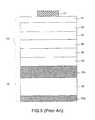
- the conventional AlGaInP LEDhas a double heterostructure (DH), which is consisted of an n-type (Al x Ga 1-x ) 0.5 In 0.5 P lower cladding layer 3 with an Al composition of about 70%-100%, formed on an n-type GaAs substrate 1 , an (Al x Ga 1-x ) 0.5 In 0.5 P active layer 5 with an Al composition of 0%-45%, a p-type (Al x Ga 1-x ) 0.5 In 0.5 P upper cladding layer 7 with an Al composition 70%-100% and a p-type high energy bandgap current spreading layer 9 such as layers of GaP, GaAsP, AlGaAs or ZnO.
- DHdouble heterostructure
- the portion of the light emits from the active layer 5 towards the substratewill be totally absorbed by GaAs substrate 1 . Therefore, the external quantum efficiency of this kind of conventional AlGaInP LED is small. Besides, the thermal conductivity of GaAs is only about 44 W/m-° C. The low thermal conductivity of the GaAs substrate 1 is not good enough to dissipate the heat generated.
- Sugawara et al.disclosed a method published in Appl. Phys. Lett. Vol. 61, 1775-1777 (1992), The LED structure is similar to the FIG. 1 , thus, in FIG. 2 , the similar function layers are labeled with the same reference numerals.
- Sugawara et al.added a distributed Bragg reflector (DBR) layer 2 in between the GaAs substrate 1 and lower cladding layer 3 so as to reflect those light emitted toward the GaAs substrate 1 , as shown in FIG. 2 . Further they added a blocking layer 10 to enhance current spread.
- DBRdistributed Bragg reflector
- the maximum reflectivity of the DBR layer 2 used in AlGaInP LEDis only about 80% and the reflectivity thereof also depends on the reflection angle.
- the DBR layer 2can only effectively reflect the light vertically emitted towards the GaAs substrate 1 , so that the improvement of external quantum efficiency is limited.
- Kish et al.disclosed a wafer-bonded transparent-substrate (TS) (Al x Ga 1-x ) 0.5 In 0.5 P/GaP light emitting diode [Appl. Phys. Lett. Vol. 64, No. 21, 2839 (1994); Very high efficiency semiconductor wafer-bonded transparent-substrate (Al x Ga 1-x ) 0.5 In 0.5 P/GaP].
- a transparent-substrate 13 (TS)is replaced for the GaAs absorption substrate (not shown).
- the TS AlGaInP LEDwas fabricated by growing a very thick (about 50 um) p-type GaP window layer 11 formed on epi-layers light emitting structure 12 (0.75 mm p-type cladding layer 3 of Al 0.5 In 0.5 P/active layer 5 of Al x Ga 1-x ) 0.5 In 0.5 P/1 mm n-type cladding layer 7 of Al 0.5 In 0.5 P with GaAs as temporary substrate by using hydride vapor phase epitaxy (HVPE). Subsequently, the temporary n-type GaAs substrate was selectively removed using conventional chemical etching techniques. After removing the GaAs substrate, the LED epilayer structure 12 is then bonded to an 8-10 mil thick n-type GaP substrate 13 .
- HVPEhydride vapor phase epitaxy
- the resulting TS AlGaInP LEDexhibits a two fold improvement in light output compared to absorbing substrate (AS) AlGaInP LEDs.
- ASabsorbing substrate
- the fabrication process of the TS AlGaInP LEDis too complicated. Therefore, it is difficult to manufacture these TS AlGaInP LEDs in high yield and low cost.
- the LED epi-layers 20is shown in FIG. 4B , which is similar to that shown in FIG. 2 , but has a GaAs buffer layer 2 a in between an n-type GaAs substrate 1 and an n-type DBR layer 2 of AlGaAs/GaAs, and a p-type GaAs capping layer 15 replaces for current spreading layer 9 .
- the mirror substrate 30is then binded with the LED epi-layers 20 by bonding the Au layer 21 with p-type capping layer 15 .
- the GaAs substrate 1 , the GaAs buffer layer 2 a , and the DBR layer 2are removed. Finally an n-type electrode of AuGeNi/Au metal layer 19 is formed on the n-type cladding layer 3 .
- the resulting structureis shown in FIG. 4 C.
- the purpose of the mirror substrate 30is to reflect the light emitted towards the absorption substrate and to provide a better thermal conductivity silicon substrate.
- the silicon of mirror substrate 30has a thermal conductivity of about 124-148 W/m-° C., and thus it can improve the heat dissipation problem.
- the top surface of AlGaInP LED epi-wafer 20normally has some hillocks (not shown). These hillocks can result in incomplete bonding regions while the LED epi-layers portion 20 bonds with the supporting substrate 30 these regions will be problematic and present deteriorated performance of LED chips.
- the n-type ohmic contact 19must be annealed at a temperature higher than 400° C.
- both p-electrode 21 and n-electrode 19are formed on the same side, so that the chip size is larger than conventional LED chip that has p-electrode on one side and n-electrode on the other side.
- the LED structureis shown in FIG. 5 , is composed of a LED epi-layers 40 and a supporting substrate 35 bonded by a low temperature solder layer 39 .
- the LED epi-layers 40is consisted of an n-type cladding layer 41 , an AlGaInP active layer 42 , a p-type cladding layer 43 , a p-type GaAs capping layer 44 and a p-type ohmic contact layer 45 .
- the supporting substrate 35is comprised an impurity heavily doped silicon substrate 36 coated with metal layers 37 a and 37 b on both sides of the silicon substrate 36 . Therefore, a vertical injection current flow LED structure with n-electrode on one side (an n-type ohmic contact metal 47 and p-electrode on the other side 37 a ) can be achieved.
- the n-ohmic contact metal 47is deposited after bonding. To achieve lower contact resistance, a high temperature annealing process is necessary but will degrade the reflectivity of metal reflector 37 b . In order not to sacrifice the reflectivity, the n-ohmic contact metal 47 can't be annealed in higher temperature. Therefore, a lower n-type ohmic contact 47 resistance can't be achieved.
- the present inventionprovides a high efficiency light emitting diode.
- the light emitting diodecomprises an LED epitaxial structure which has a plurality of III-V compound semiconductor layers grown on a lattice matched substrate and can generate light in responsive to injection current, a metal reflector composed of a transparent conductive oxide layer and a highly reflective metal layer is deposited on LED layers, a silicon substrate has a first ohmic contact metal layer on one side and a second ohmic contact metal layer on the other side and a solder layer for bonding the LED epitaxial layers and the silicon substrate together.
- FIG. 1shows a schematic view of a structure of a conventional light emitting diode.
- FIG. 2shows a light emitting diode with DBR structure to reflect the light emitted from the active layer.
- FIG. 3shows a light emitting diode with transparent substrate made by wafer bonding technology.
- FIG. 4shows a mirror-substrate AlGaInP/metal/SiO 2 /Si LED fabricated by wafer-fused technology.
- FIG. 5shows a light emitting diode with metal reflector structure and is bonded to a conductive silicon substrate.
- FIGS. 6A-6Cshows a schematic view of an AlGaInP light emitting diode structure according to the present invention.
- FIG. 7Ashows a schematic view of an AlGaInN light emitting structure according to the present invention.
- FIG. 7Bshows a schematic view of supporting substrate for an AlGaInN light emitting diode
- FIG. 8shows a schematic view of an AlGaInN light emitting diode structure according to the present invention.
- the conventional AlGaInP LEDshave many disadvantages, and thus the present invention provides a newly LED structure which comprises a transparent conductive oxide layer in between metal reflector layer and the upper side of light emitting structure solve those disadvantages present in conventional LEDs and will be described in detail as below.
- an epitaxial structure 118 of a light emitting structureis consisted of a temporary GaAs substrate 100 , an etching stop layer 102 , an n-type (Al x Ga 1-x ) 0.5 In 0.5 P lower cladding layer 104 with an Al composition of about 50%-100%, an (Al x Ga 1-x ) 0.5 In 0.5 P active layer 106 with an Al composition of about 0%-45%, a p-type (Al x Ga 1-x ) 0.5 In 0.5 P upper cladding layer 108 with an Al composition of about 50%-100%, a p-type ohmic contact layer 110 .
- the material of the etching stop layer 102can be selected from any III-V compound semiconductor material that has a lattice matched with that of the GaAs substrate 100 .
- the material of the etching stop layer 102has an etching rate much smaller than that of the GaAs substrate 100 while using an etchant mixture such as 5H 3 PO 4 :3H 2 O 2 :3H 2 O or 1NH 4 OH:35H 2 O 2 , to remove GaAs substrate 100 .
- GaInP or AlGaAscan be a good candidate of the etching stop layer 102 .
- the etching stop layer 102must also have a high carrier concentration in order to form ohmic contact easily.
- the preferred carrier concentration of etching stop layer 102is higher than 1 ⁇ 10 18 cm ⁇ 3 .
- the p-type ohmic contact layer 110(hereafter called transparent ohmic contact layer 110 ) should have a high transparency to light emitted by the active layer 106 and thus must have an energy band gap larger than that of the active layer 106 .
- the transparent ohmic contact layer 110must also have a high carrier concentration therein in order to form a lower resistance ohmic contact.
- the transparent ohmic contact layer 110can be any III-V compound of semiconductors which satisfy forgoing conditions.
- LED with light emitting in a wavelength range of about 590 nm-650 nm, AlGaAs or GaAsPis a good choice as the material of p-type ohmic contact layer 110 . In case of wavelength up to 560 nm, a GaP layer is good candidate.
- the carrier concentration of transparent ohmic contact layer 110 higher than 1 ⁇ 10 18 cm ⁇ 3is preferred.
- ohmic contact metal patterned layer 112such as Au—Be, Au—Zn or Cr—Au, is formed on the p-type ohmic contact layer 110 so as to further prompt the current evenly distributed.
- the ohmic contact metal patterned layer 112is formed either through the steps sequence of forming a p-type ohmic contact metal layer atop the p-type ohmic contact layer 110 , forming a photoresist pattern, and performing an etching step to pattern the p-type ohmic contact metal layer and performing the photoresist removal or through the steps sequence of forming a photoresist with a grid or a mesh pattern, deposing a p-type ohmic contact metal layer, and then performing a lift off step to remove the portion of poor bonding metal layer and striping the photoresist finally.
- the higher coverage ratio of ohmic contact metal patterned layer 112will reduce the light output but it will reduce the forward voltage of light emitting diode. Thus, to compromise between the light output and contact resistance, the coverage ratio of ohmic contact metal patterned layer 112 112 less than 10% is preferred.
- the resulting LED structureis then annealed in a high temperature of about 350-600 ⁇ overscore ( ) ⁇ C to achieve lower contact resistance.
- a transparent conductive oxide layer 114 and a highly reflective metal layer 116are successively deposited on the transparent ohmic contact layer 110 .
- the transparent conductive layer 114 according to the inventionis selected from one of the materials that have high conductivity, good transparency and little reaction with reflective metal layer 116 even in a high temperature.
- the highly reflective metal layer 116can be selected from Au, Al or Ag. These three metals all have reflectivity higher than 90% in the wavelength range from 560 nm to 650 nm.
- the major improvement of the present inventionis the adoption of this two layers structure metal reflector to prevent the reflective metal layer 116 from reaction with the transparent ohmic contact layer 110 .
- the reflective metalssuch as Au, Al or Ag will react with most of the III-V compound semiconductor materials in high temperature. The higher the temperature the more serious the reaction is.
- the reflectivity of the reflective metal layer 116will degrade. Adding an inert transparent conductive layer 114 such as an ITO layer in between can totally avoid the interaction between the reflective metal 116 and the transparent ohmic contact layer 110 . Therefore, the reflectivity of the highly reflective metal layer 116 will not degrade during any high temperature processing.
- the AlGaInP LED epi-wafer 118is then bonded to another high thermal and electrical conductive substrate 125 .
- a lot of semiconductors and metalssuch as Si, SiC, AlN, copper, and aluminum are good candidates for serving as the conductive substrate 125 .
- the silicon waferis cheaper and more easily to be lapped, polished and diced. Therefore, the silicon substrate is preferred, as is shown in FIG. 6 B.
- a metal layeris then coated thereon both sides of silicon substrate 120 to form ohmic contacts, 122 .
- the metal bonding layer 124is one selected from solder or metals or metal silicide such as PbSn, AuGe, AuBe, AuSi, Sn, In, and PdIn.
- the metal bonding layer 124is required to provide enough adhesion strength and current conduction.
- another diffusion barrier layer 119can be optionally deposited on the highly reflective metal layer 116 .
- the diffusion barrier layer 119can be a conductive oxide layer such as ITO, CTO and ZnO or a high melting temperature metal layer such as a layer of W, WN, Mo, or silicide.
- the highly reflective metal layer 116should have a thickness higher than that of with diffusion barrier layer 119 .
- the metal bonding layer 124 formed on the ohmic contact metal 122is for illustration, as shown in FIG. 6B rather than give a limitation.
- the metal bonding layer 124can be either formed on the diffusion barrier layer 119 or formed on reflective metal layer 116 before performing the bonding process.
- the metal bonding layercan be bonded by the ohmic contact metal itself 122 without the metal bonding layer 124 , if the selected ohmic contact metal 122 has a melting point of about 300 to 600° C.
- the absorption GaAs substrate 100is removed by mechanical lapping, chemical etching, or reactive ion etching. Then, an n-type ohmic contact 130 is deposited on the etching stop layer 102 and annealed to complete a vertically current conduction AlGaInP light emitting diode with good heat dissipation. The results LED cross-sectional view is shown in FIG. 6 C.
- the luminous efficiency of the AlGaInP LED according to the present inventionis over 30 lm/W in the wavelength range of 585 nm to 630 nm.
- the brightness of the present invention AlGaInP LEDalso increases linearly with injection current even above 100 mA. It proves that the Si wafer provides a much better heat dissipation capability than GaAs substrate.
- the present inventionnot only applied to AlGaInP LED but also can be applied to other LEDs such as AlGaAs LED, InGaAsP LED, AlGaInN LED or VCSEL devices (vertical cavity surface emitting laser).
- an AlGaInN LED epi-layer structure 215is grown on the temporary Si substrate 200 with a buffer layer 202 .
- the buffer layer 202can be an AlN amorphous or polycrystalline layer, which is deposited by a sputtering method.
- the AlGaInN LED structure 215which comprises of an n-type GaN layer 204 , an InGaN multiple quantum well (MQW) 206 , and a p-type GaN layer 208 grown by MOVPE (Metal-Organic Vapour Phase Epitaxy)
- MOVPEMetal-Organic Vapour Phase Epitaxy
- a transparent ohmic contact metal layer (TCL) 210such as Ni/Au is then deposited on the p-type GaN layer 208 and annealed to form low resistance ohmic contact.
- TCLtransparent ohmic contact metal layer
- a transparent conductive layer 212 and a highly reflective metal layer 214are successively deposited on the TCL layer 210 .
- the AlGaInN LED epi-layer structure 215 on the temporary Si substrate 200is bonded to another silicon base substrate 220 , as shown in FIG. 7 B. Similar to that shown in FIG. 6 b , the silicon base substrate 220 has an ohmic contact layer 222 on both surfaces.
- a conductive oxide layer 226 or a refractory metal layer 226is optionally deposited on the metal reflective layer 214 to prevent the metal bonding layer 224 from reacting with the reflective metal layer 214 .
- the temporary Si substrate 200 and the buffer layer 202are removed by lapping, polishing, etching or a combination thereof.
- n-type ohmic contact 218is deposited on the n-type GaN layer 204 and annealed to complete a vertically current conduction AlGaInN light emitting diode with good heat dissipation. The result is shown in FIG. 8 .
- the present inventioncan also be applied to VCSEL.
- a 650 nm-670 nm AlGaInP VCSEL with GaAs substratenormally can't operate at higher temperature due to carrier leakage and heat dissipation problem.
- the quality of DBRalso is not perfect because small refractive index difference of AlGaAs/AlAs DBR and requiring longer growth time.
- metal reflector combining with P-DBRmetal reflector combining with P-DBR, the number of AlGaAs/AlAs P-DBR pairs can be reduced and the growth time can be shorter.
- the whole VCSEL structurecan be bonded to a high thermal conductivity Si substrate; therefore, the high temperature operating characteristics can be improved.
- the LEDhas better reliability performance and can be operated at much higher current.
- the metal reflectorcan withstand higher temperature without reflectivity degradation, therefore, allowing more flexibility in chip processing.
Landscapes
- Led Devices (AREA)
Abstract
Description
1. Field of the Invention
The present invention relates to a high efficiency light emitting device, and more particularly to a III-V compound semiconductor light emitting diode with a highly reflective metal reflector therein to avoid the light absorption by the substrate.
2. Description of the Prior Art
The conventional AlGaInP LED, as shown inFIG. 1 , has a double heterostructure (DH), which is consisted of an n-type (AlxGa1-x)0.5In0.5Plower cladding layer 3 with an Al composition of about 70%-100%, formed on an n-type GaAs substrate 1, an (AlxGa1-x)0.5In0.5Pactive layer 5 with an Al composition of 0%-45%, a p-type (AlxGa1-x)0.5In0.5Pupper cladding layer 7 with an Al composition 70%-100% and a p-type high energy bandgap current spreading layer9 such as layers of GaP, GaAsP, AlGaAs or ZnO. However, the portion of the light emits from theactive layer 5 towards the substrate will be totally absorbed by GaAssubstrate 1. Therefore, the external quantum efficiency of this kind of conventional AlGaInP LED is small. Besides, the thermal conductivity of GaAs is only about 44 W/m-° C. The low thermal conductivity of theGaAs substrate 1 is not good enough to dissipate the heat generated.
To overcome the substrate absorption problem, several conventional LED fabrication technologies have been disclosed. However, those conventional technologies still have several disadvantages and limitations. For example, Sugawara et al. disclosed a method published in Appl. Phys. Lett. Vol. 61, 1775-1777 (1992), The LED structure is similar to theFIG. 1 , thus, inFIG. 2 , the similar function layers are labeled with the same reference numerals. Sugawara et al. added a distributed Bragg reflector (DBR)layer 2 in between theGaAs substrate 1 andlower cladding layer 3 so as to reflect those light emitted toward theGaAs substrate 1, as shown in FIG.2. Further they added ablocking layer 10 to enhance current spread. However, the maximum reflectivity of theDBR layer 2 used in AlGaInP LED is only about 80% and the reflectivity thereof also depends on the reflection angle. TheDBR layer 2 can only effectively reflect the light vertically emitted towards theGaAs substrate 1, so that the improvement of external quantum efficiency is limited.
Kish et al. disclosed a wafer-bonded transparent-substrate (TS) (AlxGa1-x)0.5In0.5P/GaP light emitting diode [Appl. Phys. Lett. Vol. 64, No. 21, 2839 (1994); Very high efficiency semiconductor wafer-bonded transparent-substrate (AlxGa1-x)0.5In0.5P/GaP]. As shown inFIG. 3 , a transparent-substrate13 (TS) is replaced for the GaAs absorption substrate (not shown). The TS AlGaInP LED was fabricated by growing a very thick (about 50 um) p-typeGaP window layer 11 formed on epi-layers light emitting structure12 (0.75 mm p-type cladding layer 3 of Al0.5In0.5P/active layer 5 of AlxGa1-x)0.5In0.5P/1 mm n-type cladding layer 7 of Al0.5In0.5P with GaAs as temporary substrate by using hydride vapor phase epitaxy (HVPE). Subsequently, the temporary n-type GaAs substrate was selectively removed using conventional chemical etching techniques. After removing the GaAs substrate, theLED epilayer structure 12 is then bonded to an 8-10 mil thick n-type GaP substrate 13. The resulting TS AlGaInP LED exhibits a two fold improvement in light output compared to absorbing substrate (AS) AlGaInP LEDs. However, the fabrication process of the TS AlGaInP LED is too complicated. Therefore, it is difficult to manufacture these TS AlGaInP LEDs in high yield and low cost.
Horng et al. reported a mirror-substrate (MS) AlGaInP/metal/SiO2/Si LED fabricated by wafer-fused technology [Appl. Phys. Lett. Vol. 75, No. 20, 3054 (1999); AlGaInP light-emitting diodes with mirror substrates fabricated by wafer bonding][J Electronic Materials, Vol. 30, No.8, 2001, 907; Wafer bonding of 50-mm-diameter mirror substrates to AlGaInP light-emitting diode wafers]. Please refer toFIG. 4A , They used the AuBe23/Au 21 of about 100 nm/150 nm in thickness as a mirror layer and adhered toSiO 225/Si substrate 27 to form amirror substrate 30. The LED epi-layers 20 is shown inFIG. 4B , which is similar to that shown inFIG. 2 , but has aGaAs buffer layer 2ain between an n-type GaAs substrate 1 and an n-type DBR layer 2 of AlGaAs/GaAs, and a p-typeGaAs capping layer 15 replaces for current spreading layer9. Themirror substrate 30 is then binded with the LED epi-layers 20 by bonding theAu layer 21 with p-type capping layer 15. After that, theGaAs substrate 1, theGaAs buffer layer 2a, and theDBR layer 2 are removed. Finally an n-type electrode of AuGeNi/Au metal layer 19 is formed on the n-type cladding layer 3. The resulting structure is shown in FIG.4C.
The purpose of themirror substrate 30 is to reflect the light emitted towards the absorption substrate and to provide a better thermal conductivity silicon substrate. The silicon ofmirror substrate 30 has a thermal conductivity of about 124-148 W/m-° C., and thus it can improve the heat dissipation problem. However, the top surface of AlGaInP LED epi-wafer 20 normally has some hillocks (not shown). These hillocks can result in incomplete bonding regions while the LED epi-layers portion 20 bonds with the supportingsubstrate 30 these regions will be problematic and present deteriorated performance of LED chips. Moreover, to achieve lower contact resistance, the n-typeohmic contact 19 must be annealed at a temperature higher than 400° C. At such a higher temperature annealing, the reflectivity of theAu mirror layer 21 may seriously degrade because of the reaction betweenAu layer 21 and the III-V compound semiconductor: the p-typeGaAs capping layer 15. Besides, both p-electrode 21 and n-electrode 19 are formed on the same side, so that the chip size is larger than conventional LED chip that has p-electrode on one side and n-electrode on the other side.
Chen et al. in U.S. Pat. No. 6,319,778 B1 disclosed a light emitting diode with metal reflector to increase the light output. The LED structure is shown inFIG. 5 , is composed of a LED epi-layers 40 and a supportingsubstrate 35 bonded by a lowtemperature solder layer 39. The LED epi-layers 40 is consisted of an n-type cladding layer 41, an AlGaInPactive layer 42, a p-type cladding layer 43, a p-typeGaAs capping layer 44 and a p-typeohmic contact layer 45. The supportingsubstrate 35 is comprised an impurity heavily dopedsilicon substrate 36 coated withmetal layers silicon substrate 36. Therefore, a vertical injection current flow LED structure with n-electrode on one side (an n-typeohmic contact metal 47 and p-electrode on theother side 37a) can be achieved. However, the n-ohmic contact metal 47 is deposited after bonding. To achieve lower contact resistance, a high temperature annealing process is necessary but will degrade the reflectivity ofmetal reflector 37b. In order not to sacrifice the reflectivity, the n-ohmic contact metal 47 can't be annealed in higher temperature. Therefore, a lower n-type ohmic contact 47 resistance can't be achieved.
The present invention provides a high efficiency light emitting diode. The light emitting diode comprises an LED epitaxial structure which has a plurality of III-V compound semiconductor layers grown on a lattice matched substrate and can generate light in responsive to injection current, a metal reflector composed of a transparent conductive oxide layer and a highly reflective metal layer is deposited on LED layers, a silicon substrate has a first ohmic contact metal layer on one side and a second ohmic contact metal layer on the other side and a solder layer for bonding the LED epitaxial layers and the silicon substrate together.
The foregoing aspects and many of the attendant advantages of this invention will become more readily appreciated as the same becomes better understood by reference to the following detailed description, when taken in conjunction with the accompanying drawings, wherein:
As described above, the conventional AlGaInP LEDs have many disadvantages, and thus the present invention provides a newly LED structure which comprises a transparent conductive oxide layer in between metal reflector layer and the upper side of light emitting structure solve those disadvantages present in conventional LEDs and will be described in detail as below.
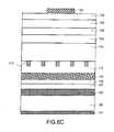
Referring toFIG. 6A , anepitaxial structure 118 of a light emitting structure is consisted of atemporary GaAs substrate 100, anetching stop layer 102, an n-type (AlxGa1-x)0.5In0.5Plower cladding layer 104 with an Al composition of about 50%-100%, an (AlxGa1-x)0.5In0.5Pactive layer 106 with an Al composition of about 0%-45%, a p-type (AlxGa1-x)0.5In0.5Pupper cladding layer 108 with an Al composition of about 50%-100%, a p-typeohmic contact layer 110.
The material of theetching stop layer 102 can be selected from any III-V compound semiconductor material that has a lattice matched with that of theGaAs substrate 100. The material of theetching stop layer 102 has an etching rate much smaller than that of theGaAs substrate 100 while using an etchant mixture such as 5H3PO4:3H2O2:3H2O or 1NH4OH:35H2O2, to removeGaAs substrate 100. For example, GaInP or AlGaAs can be a good candidate of theetching stop layer 102. Theetching stop layer 102 must also have a high carrier concentration in order to form ohmic contact easily. The preferred carrier concentration ofetching stop layer 102 is higher than 1×1018cm−3.
The p-type ohmic contact layer110 (hereafter called transparent ohmic contact layer110) should have a high transparency to light emitted by theactive layer 106 and thus must have an energy band gap larger than that of theactive layer 106. The transparentohmic contact layer 110 must also have a high carrier concentration therein in order to form a lower resistance ohmic contact. Preferably, the transparentohmic contact layer 110 can be any III-V compound of semiconductors which satisfy forgoing conditions. For example, LED with light emitting in a wavelength range of about 590 nm-650 nm, AlGaAs or GaAsP is a good choice as the material of p-typeohmic contact layer 110. In case of wavelength up to 560 nm, a GaP layer is good candidate. The carrier concentration of transparentohmic contact layer 110 higher than 1×1018cm−3is preferred.
Thereafter, a p-type ohmic contact metal grid pattern or mesh pattern112 (hereinafter called ohmic contact metal patterned layer112), such as Au—Be, Au—Zn or Cr—Au, is formed on the p-typeohmic contact layer 110 so as to further prompt the current evenly distributed. The ohmic contact metal patternedlayer 112 is formed either through the steps sequence of forming a p-type ohmic contact metal layer atop the p-typeohmic contact layer 110, forming a photoresist pattern, and performing an etching step to pattern the p-type ohmic contact metal layer and performing the photoresist removal or through the steps sequence of forming a photoresist with a grid or a mesh pattern, deposing a p-type ohmic contact metal layer, and then performing a lift off step to remove the portion of poor bonding metal layer and striping the photoresist finally.
The higher coverage ratio of ohmic contact metal patternedlayer 112 will reduce the light output but it will reduce the forward voltage of light emitting diode. Thus, to compromise between the light output and contact resistance, the coverage ratio of ohmic contact metal patternedlayer 112112 less than 10% is preferred. Thereafter, the resulting LED structure is then annealed in a high temperature of about 350-600{overscore ( )}C to achieve lower contact resistance. Then a transparentconductive oxide layer 114 and a highlyreflective metal layer 116 are successively deposited on the transparentohmic contact layer 110. The transparentconductive layer 114 according to the invention is selected from one of the materials that have high conductivity, good transparency and little reaction withreflective metal layer 116 even in a high temperature. For example, In2O3, SnO2, CdO, ZnO, ITO, CTO, CuAlO2, CuGaO2and SrCu2O2are good candidates. The highlyreflective metal layer 116 can be selected from Au, Al or Ag. These three metals all have reflectivity higher than 90% in the wavelength range from 560 nm to 650 nm. The major improvement of the present invention is the adoption of this two layers structure metal reflector to prevent thereflective metal layer 116 from reaction with the transparentohmic contact layer 110. Normally, the reflective metals such as Au, Al or Ag will react with most of the III-V compound semiconductor materials in high temperature. The higher the temperature the more serious the reaction is. When thereflective metal 116 reacted with the high conductivity transparentohmic contact layer 110, the reflectivity of thereflective metal layer 116 will degrade. Adding an inert transparentconductive layer 114 such as an ITO layer in between can totally avoid the interaction between thereflective metal 116 and the transparentohmic contact layer 110. Therefore, the reflectivity of the highlyreflective metal layer 116 will not degrade during any high temperature processing.
Subsequently, the AlGaInP LED epi-wafer 118 is then bonded to another high thermal and electricalconductive substrate 125. A lot of semiconductors and metals such as Si, SiC, AlN, copper, and aluminum are good candidates for serving as theconductive substrate 125. Especially, the silicon wafer is cheaper and more easily to be lapped, polished and diced. Therefore, the silicon substrate is preferred, as is shown in FIG.6B. After thesilicon substrate 120 is heavily doped with conductive impurities, a metal layer is then coated thereon both sides ofsilicon substrate 120 to form ohmic contacts,122. Then, either one side of theohmic contact metal 122 will bond with the AlGaInP LED epi-wafer 118 by ametal bonding layer 124. Themetal bonding layer 124 is one selected from solder or metals or metal silicide such as PbSn, AuGe, AuBe, AuSi, Sn, In, and PdIn. Themetal bonding layer 124 is required to provide enough adhesion strength and current conduction. To avoid the reaction between the metal bonding layer and the highlyreflective metal layer 116, anotherdiffusion barrier layer 119 can be optionally deposited on the highlyreflective metal layer 116. Thediffusion barrier layer 119 can be a conductive oxide layer such as ITO, CTO and ZnO or a high melting temperature metal layer such as a layer of W, WN, Mo, or silicide.
In case of without thediffusion barrier layer 119, the highlyreflective metal layer 116 should have a thickness higher than that of withdiffusion barrier layer 119. Furthermore, themetal bonding layer 124 formed on theohmic contact metal 122 is for illustration, as shown inFIG. 6B rather than give a limitation. For example, themetal bonding layer 124 can be either formed on thediffusion barrier layer 119 or formed onreflective metal layer 116 before performing the bonding process. Still, in bonding theohmic contact metal 122 ofconductive substrate 120 withreflective metal layer 116, the metal bonding layer can be bonded by the ohmic contact metal itself122 without themetal bonding layer 124, if the selectedohmic contact metal 122 has a melting point of about 300 to 600° C.
After bonding, theabsorption GaAs substrate 100 is removed by mechanical lapping, chemical etching, or reactive ion etching. Then, an n-typeohmic contact 130 is deposited on theetching stop layer 102 and annealed to complete a vertically current conduction AlGaInP light emitting diode with good heat dissipation. The results LED cross-sectional view is shown in FIG.6C.
The luminous efficiency of the AlGaInP LED according to the present invention is over 30 lm/W in the wavelength range of 585 nm to 630 nm. The brightness of the present invention AlGaInP LED also increases linearly with injection current even above 100 mA. It proves that the Si wafer provides a much better heat dissipation capability than GaAs substrate. The present invention not only applied to AlGaInP LED but also can be applied to other LEDs such as AlGaAs LED, InGaAsP LED, AlGaInN LED or VCSEL devices (vertical cavity surface emitting laser).
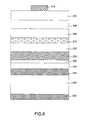
Taking the AlGaInN LED as a second preferred embodiment, an example of the AlGaInN LED epi-layer structure is shown in FIG.7A. First, an AlGaInN LED epi-layer structure 215 is grown on thetemporary Si substrate 200 with abuffer layer 202. Thebuffer layer 202 can be an AlN amorphous or polycrystalline layer, which is deposited by a sputtering method. TheAlGaInN LED structure 215 which comprises of an n-type GaN layer 204, an InGaN multiple quantum well (MQW)206, and a p-type GaN layer 208 grown by MOVPE (Metal-Organic Vapour Phase Epitaxy) A transparent ohmic contact metal layer (TCL)210 such as Ni/Au is then deposited on the p-type GaN layer 208 and annealed to form low resistance ohmic contact. Subsequently, a transparentconductive layer 212 and a highlyreflective metal layer 214 are successively deposited on theTCL layer 210.
Thereafter, the AlGaInN LED epi-layer structure 215 on thetemporary Si substrate 200 is bonded to anothersilicon base substrate 220, as shown in FIG.7B. Similar to that shown inFIG. 6 b, thesilicon base substrate 220 has anohmic contact layer 222 on both surfaces. Before bonding, aconductive oxide layer 226 or arefractory metal layer 226 is optionally deposited on the metalreflective layer 214 to prevent themetal bonding layer 224 from reacting with thereflective metal layer 214. After bonding, thetemporary Si substrate 200 and thebuffer layer 202 are removed by lapping, polishing, etching or a combination thereof. Because the hardness or chemical properties of Si and AlGaInN are quite different, it is quite easy to remove theSi substrate 200 and thebuffer layer 202 and stop at n-type GaN layer 204. Finally, an n-typeohmic contact 218 is deposited on the n-type GaN layer 204 and annealed to complete a vertically current conduction AlGaInN light emitting diode with good heat dissipation. The result is shown in FIG.8.
The present invention can also be applied to VCSEL. For example, a 650 nm-670 nm AlGaInP VCSEL with GaAs substrate normally can't operate at higher temperature due to carrier leakage and heat dissipation problem. The quality of DBR also is not perfect because small refractive index difference of AlGaAs/AlAs DBR and requiring longer growth time. Using the present invention metal reflector combining with P-DBR, the number of AlGaAs/AlAs P-DBR pairs can be reduced and the growth time can be shorter. The whole VCSEL structure can be bonded to a high thermal conductivity Si substrate; therefore, the high temperature operating characteristics can be improved.
The benefits of the present invention are:
(1) to provide an LED chip structure with vertical current flow and requiring a single wire bonding that results in easy LED assembly and the manufacturing cost can be reduced.
(2) an LED chip size can be greatly reduced and compatible with the trend toward miniaturization, particularly in surface mount LED applications and saving the material cost.
(3) with good heat dissipation, therefore, the LED has better reliability performance and can be operated at much higher current.
(4) very easy to mass-produce in higher yield and lower cost.
(5) the metal reflector can withstand higher temperature without reflectivity degradation, therefore, allowing more flexibility in chip processing.
As is understood by a person skilled in the art, the foregoing preferred embodiments of the present invention are illustrated of the present invention rather than limiting of the present invention. It is intended to cover various modifications and similar arrangements included within the spirit and scope of the appended claims, the scope of which should be accorded the broadest interpretation.
Claims (6)
1. A light emitting diode comprising:
a conductive base substrate;
a light emitting structure having a plurality of light emitting layers which generate light in responsive to an injection current;
a transparent conductive oxide layer formed on said light emitting structure, said transparent conductive oxide layer having one of an ohmic contact metal grid and a dot patterned layer formed therein and atop said light emitting structure;
a metal reflective layer formed on said transparent conductive oxide layer, said transparent conductive oxide layer being formed to prevent said metal reflective layer from reacting with said light emitting layers while annealing for improving ohmic contact of electrodes of said light emitting diode;
a diffusion barrier layer formed in between said metal reflective layer and a metal bonding layer; and
said metal bonding layer formed in between said conductive base substrate and said diffusion barrier layer so as to bond said conductive base substrate and said light emitting structure.
2. The light emitting diode according toclaim 1 , wherein said conductive base substrate is a heat dissipation and electrical conductive layer selected from the group consisting of copper, aluminum, SiC, AlN and silicon.
3. The light emitting diode according toclaim 1 , wherein said transparent conductive layer is selected from the group consisting of In2O3, SnO2, CdO, ZnO, ITO, CTO, CuAlO2, CuGaO2and SrCu2O2.
4. The light emitting diode according toclaim 1 , wherein said metal reflective layer is selected from the group consisting of Au, Al and Ag.
5. The light emitting diode according toclaim 1 , wherein said metal bonding layer is selected from the group consisting of In, Au—Sn alloy, Au—Si alloy, Pb—Sn alloy and Au—Ge alloy, PdIn.
6. The light emitting diode according toclaim 1 , wherein said diffusion barrier layer is selected from the group consisting of conductive oxide layer, refractory metal layer, and refractory metal silicide.
Priority Applications (2)
| Application Number | Priority Date | Filing Date | Title |
|---|---|---|---|
| US10/058,761US6869820B2 (en) | 2002-01-30 | 2002-01-30 | High efficiency light emitting diode and method of making the same |
| DE10211531ADE10211531B4 (en) | 2002-01-30 | 2002-03-15 | High efficiency LED and method of making same |
Applications Claiming Priority (2)
| Application Number | Priority Date | Filing Date | Title |
|---|---|---|---|
| US10/058,761US6869820B2 (en) | 2002-01-30 | 2002-01-30 | High efficiency light emitting diode and method of making the same |
| DE10211531ADE10211531B4 (en) | 2002-01-30 | 2002-03-15 | High efficiency LED and method of making same |
Publications (2)
| Publication Number | Publication Date |
|---|---|
| US20030143772A1 US20030143772A1 (en) | 2003-07-31 |
| US6869820B2true US6869820B2 (en) | 2005-03-22 |
Family
ID=30001453
Family Applications (1)
| Application Number | Title | Priority Date | Filing Date |
|---|---|---|---|
| US10/058,761Expired - LifetimeUS6869820B2 (en) | 2002-01-30 | 2002-01-30 | High efficiency light emitting diode and method of making the same |
Country Status (2)
| Country | Link |
|---|---|
| US (1) | US6869820B2 (en) |
| DE (1) | DE10211531B4 (en) |
Cited By (47)
| Publication number | Priority date | Publication date | Assignee | Title |
|---|---|---|---|---|
| US20030168664A1 (en)* | 2000-05-26 | 2003-09-11 | Berthold Hahn | Light-emitting-diode chip comprising a sequence of gan-based epitaxial layer which emit radiation, and a method for producing the same |
| US20030189212A1 (en)* | 2002-04-09 | 2003-10-09 | Yoo Myung Cheol | Method of fabricating vertical devices using a metal support film |
| US20040026709A1 (en)* | 2000-04-26 | 2004-02-12 | Stefan Bader | Gan-based light emitting-diode chip and a method for producing a luminescent diode component |
| US20040033638A1 (en)* | 2000-10-17 | 2004-02-19 | Stefan Bader | Method for fabricating a semiconductor component based on GaN |
| US20050098792A1 (en)* | 2002-04-09 | 2005-05-12 | Jong-Lam Lee | Method of fabricating vertical structure LEDs |
| US20050110037A1 (en)* | 2003-11-21 | 2005-05-26 | Sanken Electric Co., Ltd. | Light-emitting semiconductor device and method of fabrication |
| US20050191780A1 (en)* | 2003-04-15 | 2005-09-01 | Luminus Devices, Inc., A Delaware Corporation | Light emitting devices |
| US20050205886A1 (en)* | 2002-11-29 | 2005-09-22 | Sanken Electric Co., Ltd. | Gallium-containing light-emitting semiconductor device and method of fabrication |
| US20060154392A1 (en)* | 2005-01-11 | 2006-07-13 | Tran Chuong A | Method of making a vertical light emitting diode |
| US20060231854A1 (en)* | 2005-04-15 | 2006-10-19 | Samsung Electro-Mechanics Co., Ltd. | Flip chip type nitride semiconductor light emitting device |
| US20060286694A1 (en)* | 2005-06-21 | 2006-12-21 | Unit Light Technology Inc. | Method for fabricating LED |
| US20070020788A1 (en)* | 2005-07-12 | 2007-01-25 | Jin-Hsiang Liu | Fabrication method of high-brightness light emitting diode having reflective layer |
| US7205576B2 (en) | 2003-09-08 | 2007-04-17 | Samsung Electronics Co., Ltd. | Light emitting device and method of manufacturing the same |
| US20070087461A1 (en)* | 2003-03-07 | 2007-04-19 | Epitech Technology Corporation | Light emitting diode and method for manufacturing the same |
| US20070224831A1 (en)* | 2006-03-23 | 2007-09-27 | Lg Electronics Inc. | Post structure, semiconductor device and light emitting device using the structure, and method for forming the same |
| US20070290221A1 (en)* | 2006-06-16 | 2007-12-20 | Opto Tech Corporation | Light emitting diode and manufacturing method of the same |
| WO2007148866A1 (en)* | 2006-06-23 | 2007-12-27 | Lg Electronics Inc. | Light emitting diode having vertical topology and method of making the same |
| CN100442560C (en)* | 2006-05-18 | 2008-12-10 | 洲磊科技股份有限公司 | Method for manufacturing light emitting diode |
| US20080303003A1 (en)* | 2005-12-08 | 2008-12-11 | Merck Patent Gmbh | Novel Materials for Organic Electroluminescent Devices |
| US20090026473A1 (en)* | 2005-05-27 | 2009-01-29 | Lattice Power (Jiangxi) Corporation | InGaAlN LIGHT-EMITTING DEVICE AND MANUFACTURING METHOD THEREOF |
| US20090159908A1 (en)* | 2007-12-19 | 2009-06-25 | Philips Lumileds Lighting Company Llc | Semiconductor light emitting device with light extraction structures |
| US20090283747A1 (en)* | 2008-04-15 | 2009-11-19 | Mark Oliver Harwood | Metallized silicon substrate for indium gallium nitride light emitting diode |
| US20100078659A1 (en)* | 2008-09-29 | 2010-04-01 | Hitachi Cable, Ltd. | Light-emitting element |
| US7691659B2 (en) | 2000-04-26 | 2010-04-06 | Osram Gmbh | Radiation-emitting semiconductor element and method for producing the same |
| US7705363B2 (en) | 2006-11-03 | 2010-04-27 | Lg Electronics, Inc. | Light emitting device having a light extraction structure |
| US7713776B1 (en)* | 2009-08-13 | 2010-05-11 | Ray-Hua Horng | Method of making a light emitting diode |
| US20100127274A1 (en)* | 2002-06-26 | 2010-05-27 | Yoo Myung Cheol | Thin film light emitting diode |
| US20100174525A1 (en)* | 2003-02-21 | 2010-07-08 | Motionpoint Corporation | Analyzing web site for translation |
| US20100207153A1 (en)* | 2009-02-18 | 2010-08-19 | Jung Joo Yong | Semiconductor light emitting device and light emitting device package including the same |
| US20100224891A1 (en)* | 2009-03-03 | 2010-09-09 | Jizhi Zhang | VERTICALLY STRUCTURED LED BY INTEGRATING NITRIDE SEMICONDUCTORS WITH Zn(Mg,Cd,Be)O(S,Se) AND METHOD FOR MAKING SAME |
| US20100301362A1 (en)* | 2009-05-27 | 2010-12-02 | Hitachi Cable, Ltd. | Semiconductor light emitting element |
| US20110003415A1 (en)* | 2006-12-29 | 2011-01-06 | Schang-Jing Hon | High efficiency light-emitting diode and method for manufacturing the same |
| US20110220948A1 (en)* | 2001-07-17 | 2011-09-15 | Yoo Myung Cheol | Diode having high brightness and method thereof |
| US20120135551A1 (en)* | 2007-12-28 | 2012-05-31 | Seoul Opto Device Co., Ltd. | Light emitting diode and method of fabricating the same |
| US20120187398A1 (en)* | 2011-01-26 | 2012-07-26 | Woosik Lim | Light emitting device |
| CN101515613B (en)* | 2008-02-19 | 2013-04-03 | 晶元光电股份有限公司 | semiconductor element |
| US8759129B2 (en) | 2001-10-22 | 2014-06-24 | Lg Innotek Co., Ltd | Method of making diode having reflective layer |
| WO2014164983A1 (en)* | 2013-03-13 | 2014-10-09 | Intermolecular, Inc | An improved conductive transparent reflector |
| US9000468B2 (en) | 2001-10-26 | 2015-04-07 | Lg Innotek Co., Ltd. | Diode having vertical structure |
| US9128918B2 (en) | 2010-07-13 | 2015-09-08 | Motionpoint Corporation | Dynamic language translation of web site content |
| US9299886B2 (en) | 2014-01-30 | 2016-03-29 | Azur Space Solar Power Gmbh | LED semiconductor component |
| US10211370B2 (en) | 2015-09-11 | 2019-02-19 | Azur Space Solar Power Gmbh | Infrared LED |
| US10559731B1 (en)* | 2015-03-04 | 2020-02-11 | Bridgelux Inc. | Highly reliable and reflective LED substrate |
| US10573786B2 (en) | 2018-01-26 | 2020-02-25 | Samsung Electronics Co., Ltd. | Semiconductor light emitting device |
| US11063182B2 (en)* | 2017-06-01 | 2021-07-13 | Osram Oled Gmbh | Optoelectronic component and method of manufacturing an optoelectronic component |
| US11527680B2 (en)* | 2018-07-12 | 2022-12-13 | Jiangxi Zhao Chi Semiconductor Co., Ltd. | Ultraviolet light-emitting diode chip and method for making the same |
| US11563140B2 (en)* | 2018-05-02 | 2023-01-24 | Tiajin Sanan Optoelectornics Co., Ltd. | Light emitting device and production method and use thereof |
Families Citing this family (68)
| Publication number | Priority date | Publication date | Assignee | Title |
|---|---|---|---|---|
| FR2894990B1 (en)* | 2005-12-21 | 2008-02-22 | Soitec Silicon On Insulator | PROCESS FOR PRODUCING SUBSTRATES, IN PARTICULAR FOR OPTICS, ELECTRONICS OR OPTOELECTRONICS AND SUBSTRATE OBTAINED BY SAID PROCESS |
| FR2840731B3 (en)* | 2002-06-11 | 2004-07-30 | Soitec Silicon On Insulator | METHOD FOR MANUFACTURING A SUBSTRATE HAVING A USEFUL LAYER OF SINGLE-CRYSTAL SEMICONDUCTOR MATERIAL OF IMPROVED PROPERTIES |
| US8507361B2 (en) | 2000-11-27 | 2013-08-13 | Soitec | Fabrication of substrates with a useful layer of monocrystalline semiconductor material |
| TW541710B (en)* | 2001-06-27 | 2003-07-11 | Epistar Corp | LED having transparent substrate and the manufacturing method thereof |
| TW541732B (en)* | 2002-08-28 | 2003-07-11 | Arima Optoelectronics Corp | Manufacturing method of LED having transparent substrate |
| TW578318B (en)* | 2002-12-31 | 2004-03-01 | United Epitaxy Co Ltd | Light emitting diode and method of making the same |
| US20040130263A1 (en)* | 2003-01-02 | 2004-07-08 | Ray-Hua Horng | High brightness led and method for producing the same |
| US6786390B2 (en)* | 2003-02-04 | 2004-09-07 | United Epitaxy Company Ltd. | LED stack manufacturing method and its structure thereof |
| JP4217093B2 (en)* | 2003-03-27 | 2009-01-28 | スタンレー電気株式会社 | Semiconductor light emitting device and manufacturing method thereof |
| US7262550B2 (en)* | 2003-04-15 | 2007-08-28 | Luminus Devices, Inc. | Light emitting diode utilizing a physical pattern |
| US6831302B2 (en)* | 2003-04-15 | 2004-12-14 | Luminus Devices, Inc. | Light emitting devices with improved extraction efficiency |
| US7211831B2 (en)* | 2003-04-15 | 2007-05-01 | Luminus Devices, Inc. | Light emitting device with patterned surfaces |
| US7074631B2 (en)* | 2003-04-15 | 2006-07-11 | Luminus Devices, Inc. | Light emitting device methods |
| US20040259279A1 (en)* | 2003-04-15 | 2004-12-23 | Erchak Alexei A. | Light emitting device methods |
| US7667238B2 (en)* | 2003-04-15 | 2010-02-23 | Luminus Devices, Inc. | Light emitting devices for liquid crystal displays |
| US7521854B2 (en)* | 2003-04-15 | 2009-04-21 | Luminus Devices, Inc. | Patterned light emitting devices and extraction efficiencies related to the same |
| US7166871B2 (en)* | 2003-04-15 | 2007-01-23 | Luminus Devices, Inc. | Light emitting systems |
| US7084434B2 (en)* | 2003-04-15 | 2006-08-01 | Luminus Devices, Inc. | Uniform color phosphor-coated light-emitting diode |
| US7274043B2 (en)* | 2003-04-15 | 2007-09-25 | Luminus Devices, Inc. | Light emitting diode systems |
| US7105861B2 (en)* | 2003-04-15 | 2006-09-12 | Luminus Devices, Inc. | Electronic device contact structures |
| US7098589B2 (en) | 2003-04-15 | 2006-08-29 | Luminus Devices, Inc. | Light emitting devices with high light collimation |
| TWI287878B (en)* | 2003-04-16 | 2007-10-01 | Arima Optoelectronics Corp | Light-emitting diodes and method of manufacturing same using metal bonding technique |
| US7344903B2 (en)* | 2003-09-17 | 2008-03-18 | Luminus Devices, Inc. | Light emitting device processes |
| US7341880B2 (en)* | 2003-09-17 | 2008-03-11 | Luminus Devices, Inc. | Light emitting device processes |
| US20050191777A1 (en)* | 2003-09-22 | 2005-09-01 | National Chung-Hsing University | Method for producing light emitting diode with plated substrate |
| JP3979378B2 (en)* | 2003-11-06 | 2007-09-19 | 住友電気工業株式会社 | Semiconductor light emitting device |
| US7450311B2 (en) | 2003-12-12 | 2008-11-11 | Luminus Devices, Inc. | Optical display systems and methods |
| KR100576857B1 (en)* | 2003-12-24 | 2006-05-10 | 삼성전기주식회사 | BANN semiconductor light emitting device and manufacturing method thereof |
| US20050167681A1 (en)* | 2004-02-04 | 2005-08-04 | Samsung Electronics Co., Ltd. | Electrode layer, light emitting device including the same, and method of forming the electrode layer |
| TWI236837B (en)* | 2004-02-20 | 2005-07-21 | Epistar Corp | Organic adhesive light emitting element with ohmic metal protrusion |
| EP1569263B1 (en)* | 2004-02-27 | 2011-11-23 | OSRAM Opto Semiconductors GmbH | Method for joining two wafers |
| JP2005259820A (en)* | 2004-03-09 | 2005-09-22 | Sharp Corp | III-V compound semiconductor light emitting device and method for manufacturing the same |
| DE102005016592A1 (en) | 2004-04-14 | 2005-11-24 | Osram Opto Semiconductors Gmbh | LED chip |
| US20090023239A1 (en)* | 2004-07-22 | 2009-01-22 | Luminus Devices, Inc. | Light emitting device processes |
| US20060038188A1 (en)* | 2004-08-20 | 2006-02-23 | Erchak Alexei A | Light emitting diode systems |
| US20060054919A1 (en)* | 2004-08-27 | 2006-03-16 | Kyocera Corporation | Light-emitting element, method for manufacturing the same and lighting equipment using the same |
| JP4592388B2 (en)* | 2004-11-04 | 2010-12-01 | シャープ株式会社 | III-V compound semiconductor light emitting device and method for manufacturing the same |
| TWI352437B (en) | 2007-08-27 | 2011-11-11 | Epistar Corp | Optoelectronic semiconductor device |
| US7170100B2 (en) | 2005-01-21 | 2007-01-30 | Luminus Devices, Inc. | Packaging designs for LEDs |
| US7692207B2 (en)* | 2005-01-21 | 2010-04-06 | Luminus Devices, Inc. | Packaging designs for LEDs |
| US20070045640A1 (en)* | 2005-08-23 | 2007-03-01 | Erchak Alexei A | Light emitting devices for liquid crystal displays |
| KR20060131327A (en)* | 2005-06-16 | 2006-12-20 | 엘지전자 주식회사 | Manufacturing method of light emitting diode |
| US20080099777A1 (en)* | 2005-10-19 | 2008-05-01 | Luminus Devices, Inc. | Light-emitting devices and related systems |
| KR100631418B1 (en)* | 2005-11-15 | 2006-10-04 | 삼성전기주식회사 | Vertical structure gallium nitride-based light emitting diode device |
| US20070181905A1 (en)* | 2006-02-07 | 2007-08-09 | Hui-Heng Wang | Light emitting diode having enhanced side emitting capability |
| US7928462B2 (en) | 2006-02-16 | 2011-04-19 | Lg Electronics Inc. | Light emitting device having vertical structure, package thereof and method for manufacturing the same |
| US7637009B2 (en)* | 2006-02-27 | 2009-12-29 | Sv Probe Pte. Ltd. | Approach for fabricating probe elements for probe card assemblies using a reusable substrate |
| JP4406632B2 (en)* | 2006-08-31 | 2010-02-03 | アルプス電気株式会社 | Magnetic detection device and manufacturing method thereof |
| US8716728B2 (en)* | 2006-10-20 | 2014-05-06 | Mitsubishi Chemical Corporation | Nitride semiconductor light-emitting diode device |
| TWI370555B (en)* | 2006-12-29 | 2012-08-11 | Epistar Corp | Light-emitting diode and method for manufacturing the same |
| US8110425B2 (en) | 2007-03-20 | 2012-02-07 | Luminus Devices, Inc. | Laser liftoff structure and related methods |
| CN101308887B (en)* | 2007-05-18 | 2010-09-29 | 富士迈半导体精密工业(上海)有限公司 | High-brightness light-emitting diode and its manufacturing method |
| US8546818B2 (en)* | 2007-06-12 | 2013-10-01 | SemiLEDs Optoelectronics Co., Ltd. | Vertical LED with current-guiding structure |
| DE102008013900A1 (en)* | 2008-03-12 | 2009-09-17 | Osram Opto Semiconductors Gmbh | Method for producing a multiplicity of optoelectronic semiconductor chips and optoelectronic semiconductor chip |
| US20100019222A1 (en)* | 2008-07-25 | 2010-01-28 | High Power Opto.Inc. | Low-temperature led chip metal bonding layer |
| JP2009296007A (en)* | 2009-09-16 | 2009-12-17 | Sharp Corp | Group iii-v compound semiconductor light emitting element |
| JP2011103400A (en)* | 2009-11-11 | 2011-05-26 | Sumitomo Electric Ind Ltd | Compound semiconductor element |
| KR20110085609A (en)* | 2010-01-21 | 2011-07-27 | 엘지이노텍 주식회사 | Light emitting device and manufacturing method |
| CN101872830A (en)* | 2010-06-10 | 2010-10-27 | 厦门市三安光电科技有限公司 | Vertical light-emitting diodes with built-in short-circuit protection |
| CN102313247A (en)* | 2011-09-26 | 2012-01-11 | 江门市三泰照明制品有限公司 | Reflector for light emitting diode (LED) lamp |
| CN108054261A (en)* | 2012-02-14 | 2018-05-18 | 晶元光电股份有限公司 | Light emitting element having current diffusion layer with flat surface |
| US9082692B2 (en) | 2013-01-02 | 2015-07-14 | Micron Technology, Inc. | Engineered substrate assemblies with epitaxial templates and related systems, methods, and devices |
| CN103996755B (en)* | 2014-05-21 | 2016-08-17 | 天津三安光电有限公司 | A kind of preparation method of iii-nitride light emitting devices assembly |
| WO2016122725A1 (en)* | 2015-01-30 | 2016-08-04 | Technologies Llc Sxaymiq | Micro-light emitting diode with metal side mirror |
| CN113571622B (en)* | 2021-07-22 | 2022-08-23 | 厦门三安光电有限公司 | Light emitting diode and method for manufacturing the same |
| CN114639763B (en)* | 2022-05-12 | 2022-09-06 | 南昌凯捷半导体科技有限公司 | A kind of reverse polarity infrared LED with embedded electrode and preparation method thereof |
| CN116544322A (en)* | 2023-07-06 | 2023-08-04 | 江西兆驰半导体有限公司 | A GaAs-based LED chip, preparation method and LED |
| CN119630184B (en)* | 2025-02-12 | 2025-07-11 | 合肥晶合集成电路股份有限公司 | OLED micro-resonant cavity structure and manufacturing method thereof |
Citations (8)
| Publication number | Priority date | Publication date | Assignee | Title |
|---|---|---|---|---|
| US20010004534A1 (en)* | 1999-05-24 | 2001-06-21 | Carrie Carter-Coman | Diffusion barrier for increased mirror reflectivity in reflective solderable contacts on high power led chip |
| US20020093023A1 (en)* | 1997-06-03 | 2002-07-18 | Camras Michael D. | III-Phosphide and III-Arsenide flip chip light-emitting devices |
| US6448102B1 (en)* | 1998-12-30 | 2002-09-10 | Xerox Corporation | Method for nitride based laser diode with growth substrate removed |
| US6468824B2 (en)* | 2001-03-22 | 2002-10-22 | Uni Light Technology Inc. | Method for forming a semiconductor device having a metallic substrate |
| US20030003613A1 (en)* | 2001-06-27 | 2003-01-02 | Min-Hsun Hsieh | Light emitting diode having a transparent substrate and a method for manufacturing the same |
| US6562648B1 (en)* | 2000-08-23 | 2003-05-13 | Xerox Corporation | Structure and method for separation and transfer of semiconductor thin films onto dissimilar substrate materials |
| US6607931B2 (en)* | 2000-02-24 | 2003-08-19 | Osram Opto Semiconductors Gmbh & Co. Ohg | Method of producing an optically transparent substrate and method of producing a light-emitting semiconductor chip |
| US6649437B1 (en)* | 2002-08-20 | 2003-11-18 | United Epitaxy Company, Ltd. | Method of manufacturing high-power light emitting diodes |
Family Cites Families (4)
| Publication number | Priority date | Publication date | Assignee | Title |
|---|---|---|---|---|
| US6078064A (en)* | 1998-05-04 | 2000-06-20 | Epistar Co. | Indium gallium nitride light emitting diode |
| US20010042866A1 (en)* | 1999-02-05 | 2001-11-22 | Carrie Carter Coman | Inxalygazn optical emitters fabricated via substrate removal |
| JP4409684B2 (en)* | 1999-11-17 | 2010-02-03 | 昭和電工株式会社 | AlGaInP light emitting diode and manufacturing method thereof |
| DE10026254A1 (en)* | 2000-04-26 | 2001-11-08 | Osram Opto Semiconductors Gmbh | Radiation-emitting semiconductor element has a semiconductor body formed by a stack of different semiconductor layers based on gallium nitride |
- 2002
- 2002-01-30USUS10/058,761patent/US6869820B2/ennot_activeExpired - Lifetime
- 2002-03-15DEDE10211531Apatent/DE10211531B4/ennot_activeExpired - Lifetime
Patent Citations (8)
| Publication number | Priority date | Publication date | Assignee | Title |
|---|---|---|---|---|
| US20020093023A1 (en)* | 1997-06-03 | 2002-07-18 | Camras Michael D. | III-Phosphide and III-Arsenide flip chip light-emitting devices |
| US6448102B1 (en)* | 1998-12-30 | 2002-09-10 | Xerox Corporation | Method for nitride based laser diode with growth substrate removed |
| US20010004534A1 (en)* | 1999-05-24 | 2001-06-21 | Carrie Carter-Coman | Diffusion barrier for increased mirror reflectivity in reflective solderable contacts on high power led chip |
| US6607931B2 (en)* | 2000-02-24 | 2003-08-19 | Osram Opto Semiconductors Gmbh & Co. Ohg | Method of producing an optically transparent substrate and method of producing a light-emitting semiconductor chip |
| US6562648B1 (en)* | 2000-08-23 | 2003-05-13 | Xerox Corporation | Structure and method for separation and transfer of semiconductor thin films onto dissimilar substrate materials |
| US6468824B2 (en)* | 2001-03-22 | 2002-10-22 | Uni Light Technology Inc. | Method for forming a semiconductor device having a metallic substrate |
| US20030003613A1 (en)* | 2001-06-27 | 2003-01-02 | Min-Hsun Hsieh | Light emitting diode having a transparent substrate and a method for manufacturing the same |
| US6649437B1 (en)* | 2002-08-20 | 2003-11-18 | United Epitaxy Company, Ltd. | Method of manufacturing high-power light emitting diodes |
Cited By (188)
| Publication number | Priority date | Publication date | Assignee | Title |
|---|---|---|---|---|
| US20070012944A1 (en)* | 2000-04-26 | 2007-01-18 | Stefan Bader | GaN-based light emitting-diode chip and a method for producing same |
| US7319247B2 (en) | 2000-04-26 | 2008-01-15 | Osram Gmbh | Light emitting-diode chip and a method for producing same |
| US20040026709A1 (en)* | 2000-04-26 | 2004-02-12 | Stefan Bader | Gan-based light emitting-diode chip and a method for producing a luminescent diode component |
| US7691659B2 (en) | 2000-04-26 | 2010-04-06 | Osram Gmbh | Radiation-emitting semiconductor element and method for producing the same |
| US7265392B2 (en) | 2000-05-26 | 2007-09-04 | Osram Gmbh | Light-emitting-diode chip comprising a sequence of GaN-based epitaxial layers which emit radiation and a method for producing the same |
| US7939844B2 (en) | 2000-05-26 | 2011-05-10 | Osram Gmbh | Light-emitting-diode chip comprising a sequence of GAN-based epitaxial layers which emit radiation and a method for producing the same |
| US8436393B2 (en) | 2000-05-26 | 2013-05-07 | Osram Gmbh | Light-emitting-diode chip comprising a sequence of GaN-based epitaxial layers which emit radiation and a method for producing the same |
| US20070221936A1 (en)* | 2000-05-26 | 2007-09-27 | Osram Gmbh | Light-emitting-diode chip comprising a sequence of gan-based epitaxial layers which emit radiation and a method for producing the same |
| US20110175058A1 (en)* | 2000-05-26 | 2011-07-21 | Berthold Hahn | LIGHT-EMITTING-DIODE CHIP COMPRISING A SEQUENCE OF GaN-BASED EPITAXIAL LAYERS WHICH EMIT RADIATION AND A METHOD FOR PRODUCING THE SAME |
| US20030168664A1 (en)* | 2000-05-26 | 2003-09-11 | Berthold Hahn | Light-emitting-diode chip comprising a sequence of gan-based epitaxial layer which emit radiation, and a method for producing the same |
| US20100200864A1 (en)* | 2000-10-17 | 2010-08-12 | Osram Gmbh | Method for Fabricating a Semiconductor Component Based on GaN |
| US8809086B2 (en) | 2000-10-17 | 2014-08-19 | Osram Gmbh | Method for fabricating a semiconductor component based on GaN |
| US7691656B2 (en) | 2000-10-17 | 2010-04-06 | Osram Gmbh | Method for fabricating a semiconductor component based on GaN |
| US8129209B2 (en) | 2000-10-17 | 2012-03-06 | Osram Ag | Method for fabricating a semiconductor component based on GaN |
| US20040033638A1 (en)* | 2000-10-17 | 2004-02-19 | Stefan Bader | Method for fabricating a semiconductor component based on GaN |
| US10553744B2 (en) | 2001-07-17 | 2020-02-04 | Lg Innotek Co., Ltd. | Diode having high brightness and method thereof |
| US9136424B2 (en) | 2001-07-17 | 2015-09-15 | Lg Innotek Co., Ltd. | Diode having high brightness and method thereof |
| US9640713B2 (en) | 2001-07-17 | 2017-05-02 | Lg Innotek Co., Ltd. | Diode having high brightness and method thereof |
| US8674386B2 (en)* | 2001-07-17 | 2014-03-18 | Lg Innotek Co. Ltd. | Diode having high brightness and method thereof |
| US20110220948A1 (en)* | 2001-07-17 | 2011-09-15 | Yoo Myung Cheol | Diode having high brightness and method thereof |
| US10147841B2 (en) | 2001-07-17 | 2018-12-04 | Lg Innotek Co., Ltd. | Diode having high brightness and method thereof |
| US9406837B2 (en) | 2001-10-22 | 2016-08-02 | Lg Innotek Co., Ltd | Method of making diode having reflective layer |
| US8759129B2 (en) | 2001-10-22 | 2014-06-24 | Lg Innotek Co., Ltd | Method of making diode having reflective layer |
| US9620677B2 (en) | 2001-10-26 | 2017-04-11 | Lg Innotek Co., Ltd. | Diode having vertical structure |
| US10326055B2 (en) | 2001-10-26 | 2019-06-18 | Lg Innotek Co., Ltd. | Diode having vertical structure |
| US9000468B2 (en) | 2001-10-26 | 2015-04-07 | Lg Innotek Co., Ltd. | Diode having vertical structure |
| US10032959B2 (en) | 2001-10-26 | 2018-07-24 | Lg Innotek Co., Ltd. | Diode having vertical structure |
| US7250638B2 (en) | 2002-04-09 | 2007-07-31 | Lg Electronics Inc. | Method of fabricating vertical structure LEDs |
| US10644200B2 (en) | 2002-04-09 | 2020-05-05 | Lg Innotek Co., Ltd. | Vertical topology light emitting device |
| US9847455B2 (en) | 2002-04-09 | 2017-12-19 | Lg Innotek Co., Ltd. | Vertical topology light emitting device |
| US20080001166A1 (en)* | 2002-04-09 | 2008-01-03 | Jong-Lam Lee | Method of fabricating vertical structure leds |
| US10147847B2 (en) | 2002-04-09 | 2018-12-04 | Lg Innotek Co., Ltd. | Vertical topology light emitting device |
| US8106417B2 (en)* | 2002-04-09 | 2012-01-31 | Lg Electronics Inc. | Vertical topology light emitting device using a conductive support structure |
| US20080064132A1 (en)* | 2002-04-09 | 2008-03-13 | Yoo Myung C | Method of fabricating vertical devices using a metal support film |
| US10243101B2 (en) | 2002-04-09 | 2019-03-26 | Lg Innotek Co., Ltd. | Vertical structure LEDs |
| US8022386B2 (en)* | 2002-04-09 | 2011-09-20 | Lg Electronics Inc. | Vertical topology light emitting device |
| US20030189212A1 (en)* | 2002-04-09 | 2003-10-09 | Yoo Myung Cheol | Method of fabricating vertical devices using a metal support film |
| US10453993B1 (en) | 2002-04-09 | 2019-10-22 | Lg Innotek Co., Ltd. | Vertical structure LEDs |
| US7462881B2 (en) | 2002-04-09 | 2008-12-09 | Lg Electronics Inc. | Method of fabricating vertical structure LEDs |
| US9478709B2 (en)* | 2002-04-09 | 2016-10-25 | Lg Innotek Co., Ltd. | Vertical topology light emitting device |
| US9472727B2 (en) | 2002-04-09 | 2016-10-18 | Lg Innotek Co., Ltd. | Vertical structure LEDs |
| US20070018173A1 (en)* | 2002-04-09 | 2007-01-25 | Yoo Myung C | Method of fabricating vertical devices using a metal support film |
| US8294172B2 (en)* | 2002-04-09 | 2012-10-23 | Lg Electronics Inc. | Method of fabricating vertical devices using a metal support film |
| US20090072264A1 (en)* | 2002-04-09 | 2009-03-19 | Yoo Myung Cheol | Method of fabricating vertical Devices using a metal support film |
| US9224907B2 (en) | 2002-04-09 | 2015-12-29 | Lg Innotek Co., Ltd. | Vertical structure LEDs |
| US9209360B2 (en) | 2002-04-09 | 2015-12-08 | Lg Innotek Co., Ltd. | Vertical topology light-emitting device |
| US7563629B2 (en) | 2002-04-09 | 2009-07-21 | Lg Electronics Inc. | Method of fabricating vertical structure LEDs |
| US20110193128A1 (en)* | 2002-04-09 | 2011-08-11 | Jong Lam Lee | Method of fabricating vertical structure leds |
| US7569865B2 (en) | 2002-04-09 | 2009-08-04 | Lg Electronics Inc. | Method of fabricating vertical structure LEDs |
| US7576368B2 (en) | 2002-04-09 | 2009-08-18 | Lg Electronics Inc. | Method of fabricating vertical structure LEDs |
| US7588952B2 (en)* | 2002-04-09 | 2009-09-15 | Lg Electronics Inc. | Method of fabricating vertical structure LEDs |
| US20090278161A1 (en)* | 2002-04-09 | 2009-11-12 | Jong-Lam Lee | Method of fabricating vertical structure LEDs |
| US10453998B2 (en) | 2002-04-09 | 2019-10-22 | Lg Innotek Co. Ltd. | Vertical topology light emitting device |
| US20060244001A1 (en)* | 2002-04-09 | 2006-11-02 | Lg Electronic Inc. | Method of fabricating vertical structure LEDs |
| US10461217B2 (en) | 2002-04-09 | 2019-10-29 | Lg Innotek Co., Ltd. | Vertical structure LEDs |
| US10600933B2 (en) | 2002-04-09 | 2020-03-24 | Lg Innotek Co., Ltd. | Vertical structure LEDs |
| US9000477B2 (en) | 2002-04-09 | 2015-04-07 | Lg Innotek Co., Ltd. | Vertical topology light-emitting device |
| US8896017B2 (en) | 2002-04-09 | 2014-11-25 | Lg Innotek Co., Ltd. | Vertical structure LEDs |
| US8368115B2 (en)* | 2002-04-09 | 2013-02-05 | Lg Electronics Inc. | Method of fabricating vertical devices using a metal support film |
| US20050098792A1 (en)* | 2002-04-09 | 2005-05-12 | Jong-Lam Lee | Method of fabricating vertical structure LEDs |
| US7928465B2 (en) | 2002-04-09 | 2011-04-19 | Lg Electronics Inc. | Method of fabricating vertical structure LEDs |
| US20060097277A1 (en)* | 2002-04-09 | 2006-05-11 | Yoo Myung C | Method of fabricating vertical devices using a metal support film |
| US8809898B2 (en) | 2002-04-09 | 2014-08-19 | Lg Innotek Co., Ltd. | Method of fabricating vertical structure LEDs |
| US20060099730A1 (en)* | 2002-04-09 | 2006-05-11 | Lg Electronics Inc. | Method of fabricating vertical structure LEDs |
| US7772020B2 (en) | 2002-04-09 | 2010-08-10 | Lg Electronics Inc. | Method of fabricating vertical devices using a metal support film |
| US20060071230A1 (en)* | 2002-04-09 | 2006-04-06 | Lg Electronics Inc. | Method of fabricating vertical structure LEDs |
| US8384120B2 (en) | 2002-04-09 | 2013-02-26 | Lg Electronics Inc. | Method of fabricating vertical structure LEDs |
| US9882084B2 (en) | 2002-04-09 | 2018-01-30 | Lg Innotek Co., Ltd. | Vertical structure LEDs |
| US8669587B2 (en) | 2002-04-09 | 2014-03-11 | Lg Innotek Co., Ltd. | Vertical topology light emitting device |
| US7816705B2 (en) | 2002-04-09 | 2010-10-19 | Lg Electronics Inc. | Method of fabricating vertical structure LEDs |
| US8564016B2 (en)* | 2002-04-09 | 2013-10-22 | Lg Electronics Inc. | Vertical topology light emitting device |
| US20100308368A1 (en)* | 2002-04-09 | 2010-12-09 | Jong-Lam Lee | Method of fabricating vertical structure leds |
| US20100127274A1 (en)* | 2002-06-26 | 2010-05-27 | Yoo Myung Cheol | Thin film light emitting diode |
| US9281454B2 (en) | 2002-06-26 | 2016-03-08 | Lg Innotek Co., Ltd. | Thin film light emitting diode |
| US8384091B2 (en) | 2002-06-26 | 2013-02-26 | Lg Electronics Inc. | Thin film light emitting diode |
| US20100207145A1 (en)* | 2002-06-26 | 2010-08-19 | Yoo Myung Cheol | Thin film light emitting diode |
| US20100171125A1 (en)* | 2002-06-26 | 2010-07-08 | Yoo Myung Cheol | Thin film light emitting diode |
| US10825962B2 (en) | 2002-06-26 | 2020-11-03 | Lg Innotek Co., Ltd. | Thin film light emitting diode |
| US9716213B2 (en) | 2002-06-26 | 2017-07-25 | Lg Innotek Co., Ltd. | Thin film light emitting diode |
| US8207552B2 (en) | 2002-06-26 | 2012-06-26 | Lg Electronics Inc. | Thin film light emitting diode |
| US8445921B2 (en) | 2002-06-26 | 2013-05-21 | Lg Electronics, Inc. | Thin film light emitting diode |
| US20100129943A1 (en)* | 2002-06-26 | 2010-05-27 | Yoo Myung Cheol | Thin film light emitting diode |
| US7956364B2 (en) | 2002-06-26 | 2011-06-07 | Lg Electronics Inc. | Thin film light emitting diode |
| US8288787B2 (en) | 2002-06-26 | 2012-10-16 | Lg Electronics, Inc. | Thin film light emitting diode |
| US10326059B2 (en) | 2002-06-26 | 2019-06-18 | Lg Innotek Co., Ltd. | Thin film light emitting diode |
| US20080166828A1 (en)* | 2002-11-29 | 2008-07-10 | Sanken Electric Co., Ltd. | Gallium-containing light-emitting semiconductor device and method of fabrication |
| US7566576B2 (en) | 2002-11-29 | 2009-07-28 | Sanken Electric Co., Ltd. | Gallium-containing light-emitting semiconductor device and method of fabrication |
| US20050205886A1 (en)* | 2002-11-29 | 2005-09-22 | Sanken Electric Co., Ltd. | Gallium-containing light-emitting semiconductor device and method of fabrication |
| US9626360B2 (en) | 2003-02-21 | 2017-04-18 | Motionpoint Corporation | Analyzing web site for translation |
| US9652455B2 (en) | 2003-02-21 | 2017-05-16 | Motionpoint Corporation | Dynamic language translation of web site content |
| US11308288B2 (en) | 2003-02-21 | 2022-04-19 | Motionpoint Corporation | Automation tool for web site content language translation |
| US9367540B2 (en) | 2003-02-21 | 2016-06-14 | Motionpoint Corporation | Dynamic language translation of web site content |
| US10409918B2 (en) | 2003-02-21 | 2019-09-10 | Motionpoint Corporation | Automation tool for web site content language translation |
| US10621287B2 (en) | 2003-02-21 | 2020-04-14 | Motionpoint Corporation | Dynamic language translation of web site content |
| US8949223B2 (en) | 2003-02-21 | 2015-02-03 | Motionpoint Corporation | Dynamic language translation of web site content |
| US20100174525A1 (en)* | 2003-02-21 | 2010-07-08 | Motionpoint Corporation | Analyzing web site for translation |
| US20110209038A1 (en)* | 2003-02-21 | 2011-08-25 | Motionpoint Corporation | Dynamic language translation of web site content |
| US8566710B2 (en) | 2003-02-21 | 2013-10-22 | Motionpoint Corporation | Analyzing web site for translation |
| US8433718B2 (en) | 2003-02-21 | 2013-04-30 | Motionpoint Corporation | Dynamic language translation of web site content |
| US9910853B2 (en) | 2003-02-21 | 2018-03-06 | Motionpoint Corporation | Dynamic language translation of web site content |
| US20070087461A1 (en)* | 2003-03-07 | 2007-04-19 | Epitech Technology Corporation | Light emitting diode and method for manufacturing the same |
| US20050191780A1 (en)* | 2003-04-15 | 2005-09-01 | Luminus Devices, Inc., A Delaware Corporation | Light emitting devices |
| US7422915B2 (en)* | 2003-07-03 | 2008-09-09 | Epistar Corporation | Light emitting diode and method for manufacturing the same |
| US7205576B2 (en) | 2003-09-08 | 2007-04-17 | Samsung Electronics Co., Ltd. | Light emitting device and method of manufacturing the same |
| US7541207B2 (en) | 2003-09-08 | 2009-06-02 | Samsung Electronics Co., Ltd. | Light emitting device and method of manufacturing the same |
| US20070254391A1 (en)* | 2003-09-08 | 2007-11-01 | Samsung Electronics Co., Ltd. | Light emitting device and method of manufacturing the same |
| US20050110037A1 (en)* | 2003-11-21 | 2005-05-26 | Sanken Electric Co., Ltd. | Light-emitting semiconductor device and method of fabrication |
| US7087933B2 (en)* | 2003-11-21 | 2006-08-08 | Sanken Electric Co., Ltd. | Light-emitting semiconductor device and method of fabrication |
| US7413918B2 (en)* | 2005-01-11 | 2008-08-19 | Semileds Corporation | Method of making a light emitting diode |
| US8552451B2 (en) | 2005-01-11 | 2013-10-08 | SemiLEDs Optoelectronics Co., Ltd. | Light-emitting diode with increased light extraction |
| US20060154392A1 (en)* | 2005-01-11 | 2006-07-13 | Tran Chuong A | Method of making a vertical light emitting diode |
| US20090014743A1 (en)* | 2005-01-11 | 2009-01-15 | Chuong Anh Tran | Method of making a light-emitting diode |
| US8008678B2 (en) | 2005-01-11 | 2011-08-30 | Semileds Corporation | Light-emitting diode with increased light extraction |
| US20060231854A1 (en)* | 2005-04-15 | 2006-10-19 | Samsung Electro-Mechanics Co., Ltd. | Flip chip type nitride semiconductor light emitting device |
| US7297988B2 (en) | 2005-04-15 | 2007-11-20 | Samsung Electro-Mechanics Co., Ltd. | Flip chip type nitride semiconductor light emitting device |
| US8384100B2 (en)* | 2005-05-27 | 2013-02-26 | Lattice Power (Jiangxi) Corporation | InGaAIN light-emitting device and manufacturing method thereof |
| US20090026473A1 (en)* | 2005-05-27 | 2009-01-29 | Lattice Power (Jiangxi) Corporation | InGaAlN LIGHT-EMITTING DEVICE AND MANUFACTURING METHOD THEREOF |
| US20060286694A1 (en)* | 2005-06-21 | 2006-12-21 | Unit Light Technology Inc. | Method for fabricating LED |
| US7384808B2 (en)* | 2005-07-12 | 2008-06-10 | Visual Photonics Epitaxy Co., Ltd. | Fabrication method of high-brightness light emitting diode having reflective layer |
| US20070020788A1 (en)* | 2005-07-12 | 2007-01-25 | Jin-Hsiang Liu | Fabrication method of high-brightness light emitting diode having reflective layer |
| US20080303003A1 (en)* | 2005-12-08 | 2008-12-11 | Merck Patent Gmbh | Novel Materials for Organic Electroluminescent Devices |
| US7867885B2 (en)* | 2006-03-23 | 2011-01-11 | Lg Electronics Inc. | Post structure, semiconductor device and light emitting device using the structure, and method for forming the same |
| US20070224831A1 (en)* | 2006-03-23 | 2007-09-27 | Lg Electronics Inc. | Post structure, semiconductor device and light emitting device using the structure, and method for forming the same |
| CN100442560C (en)* | 2006-05-18 | 2008-12-10 | 洲磊科技股份有限公司 | Method for manufacturing light emitting diode |
| US20070290221A1 (en)* | 2006-06-16 | 2007-12-20 | Opto Tech Corporation | Light emitting diode and manufacturing method of the same |
| US7768025B2 (en) | 2006-06-23 | 2010-08-03 | Lg Electronics Inc. | Light emitting diode having vertical topology and method of making the same |
| US20070295952A1 (en)* | 2006-06-23 | 2007-12-27 | Lg Electronics Inc. | Light Emitting Diode having vertical topology and method of making the same |
| US20080023691A1 (en)* | 2006-06-23 | 2008-01-31 | Jang Jun H | Light emitting diode having vertical topology and method of making the same |
| US8624288B2 (en) | 2006-06-23 | 2014-01-07 | Lg Electronics, Inc. | Light emitting diode having vertical topology and method of making the same |
| US8039281B2 (en) | 2006-06-23 | 2011-10-18 | Lg Electronics Inc. | Light emitting diode having vertical topology and method of making the same |
| US7834374B2 (en) | 2006-06-23 | 2010-11-16 | Lg Electronics Inc. | Light emitting diode having vertical topology and method of making the same |
| WO2007148866A1 (en)* | 2006-06-23 | 2007-12-27 | Lg Electronics Inc. | Light emitting diode having vertical topology and method of making the same |
| US9530936B2 (en) | 2006-06-23 | 2016-12-27 | Lg Electronics Inc. | Light emitting diode having vertical topology and method of making the same |
| US20110003416A1 (en)* | 2006-06-23 | 2011-01-06 | Jun Ho Jang | Light emitting diode having vertical topology and method of making the same |
| US7705363B2 (en) | 2006-11-03 | 2010-04-27 | Lg Electronics, Inc. | Light emitting device having a light extraction structure |
| US20110003415A1 (en)* | 2006-12-29 | 2011-01-06 | Schang-Jing Hon | High efficiency light-emitting diode and method for manufacturing the same |
| US8546156B2 (en)* | 2006-12-29 | 2013-10-01 | Epistar Corporation | High efficiency light-emitting diode and method for manufacturing the same |
| US10164155B2 (en) | 2007-12-19 | 2018-12-25 | Lumileds Llc | Semiconductor light emitting device with light extraction structures |
| US7985979B2 (en) | 2007-12-19 | 2011-07-26 | Koninklijke Philips Electronics, N.V. | Semiconductor light emitting device with light extraction structures |
| US8242521B2 (en) | 2007-12-19 | 2012-08-14 | Koninklijke Philips Electronics N.V. | Semiconductor light emitting device with light extraction structures |
| US10734553B2 (en) | 2007-12-19 | 2020-08-04 | Lumileds Llc | Semiconductor light emitting device with light extraction structures |
| US20090159908A1 (en)* | 2007-12-19 | 2009-06-25 | Philips Lumileds Lighting Company Llc | Semiconductor light emitting device with light extraction structures |
| US9142726B2 (en) | 2007-12-19 | 2015-09-22 | Philips Lumileds Lighting Company Llc | Semiconductor light emitting device with light extraction structures |
| US9935242B2 (en) | 2007-12-19 | 2018-04-03 | Lumileds Llc | Semiconductor light emitting device with light extraction structures |
| US8628983B2 (en)* | 2007-12-28 | 2014-01-14 | Seoul Opto Device Co., Ltd. | Light emitting diode and method of fabricating the same |
| US20120135551A1 (en)* | 2007-12-28 | 2012-05-31 | Seoul Opto Device Co., Ltd. | Light emitting diode and method of fabricating the same |
| CN101515613B (en)* | 2008-02-19 | 2013-04-03 | 晶元光电股份有限公司 | semiconductor element |
| US20100176369A2 (en)* | 2008-04-15 | 2010-07-15 | Mark Oliver | Metalized Silicon Substrate for Indium Gallium Nitride Light-Emitting Diodes |
| US20090283747A1 (en)* | 2008-04-15 | 2009-11-19 | Mark Oliver Harwood | Metallized silicon substrate for indium gallium nitride light emitting diode |
| US8120046B2 (en)* | 2008-09-29 | 2012-02-21 | Hitachi Cable, Ltd. | Light-emitting element |
| US20100078659A1 (en)* | 2008-09-29 | 2010-04-01 | Hitachi Cable, Ltd. | Light-emitting element |
| US20100207153A1 (en)* | 2009-02-18 | 2010-08-19 | Jung Joo Yong | Semiconductor light emitting device and light emitting device package including the same |
| US8421103B2 (en)* | 2009-02-18 | 2013-04-16 | Lg Innotek Co., Ltd. | Semiconductor light emitting device and light emitting device package including the same |
| US8642369B2 (en)* | 2009-03-03 | 2014-02-04 | Zn Technology, Inc. | Vertically structured LED by integrating nitride semiconductors with Zn(Mg,Cd,Be)O(S,Se) and method for making same |
| US20100224891A1 (en)* | 2009-03-03 | 2010-09-09 | Jizhi Zhang | VERTICALLY STRUCTURED LED BY INTEGRATING NITRIDE SEMICONDUCTORS WITH Zn(Mg,Cd,Be)O(S,Se) AND METHOD FOR MAKING SAME |
| US8120051B2 (en)* | 2009-05-27 | 2012-02-21 | Hitachi Cable, Ltd. | Semiconductor light emitting element |
| US20100301362A1 (en)* | 2009-05-27 | 2010-12-02 | Hitachi Cable, Ltd. | Semiconductor light emitting element |
| US7713776B1 (en)* | 2009-08-13 | 2010-05-11 | Ray-Hua Horng | Method of making a light emitting diode |
| US9311287B2 (en) | 2010-07-13 | 2016-04-12 | Motionpoint Corporation | Dynamic language translation of web site content |
| US9858347B2 (en) | 2010-07-13 | 2018-01-02 | Motionpoint Corporation | Dynamic language translation of web site content |
| US10296651B2 (en) | 2010-07-13 | 2019-05-21 | Motionpoint Corporation | Dynamic language translation of web site content |
| US11481463B2 (en) | 2010-07-13 | 2022-10-25 | Motionpoint Corporation | Dynamic language translation of web site content |
| US11409828B2 (en) | 2010-07-13 | 2022-08-09 | Motionpoint Corporation | Dynamic language translation of web site content |
| US10387517B2 (en) | 2010-07-13 | 2019-08-20 | Motionpoint Corporation | Dynamic language translation of web site content |
| US9465782B2 (en) | 2010-07-13 | 2016-10-11 | Motionpoint Corporation | Dynamic language translation of web site content |
| US10146884B2 (en) | 2010-07-13 | 2018-12-04 | Motionpoint Corporation | Dynamic language translation of web site content |
| US9411793B2 (en) | 2010-07-13 | 2016-08-09 | Motionpoint Corporation | Dynamic language translation of web site content |
| US10089400B2 (en) | 2010-07-13 | 2018-10-02 | Motionpoint Corporation | Dynamic language translation of web site content |
| US10073917B2 (en) | 2010-07-13 | 2018-09-11 | Motionpoint Corporation | Dynamic language translation of web site content |
| US9864809B2 (en) | 2010-07-13 | 2018-01-09 | Motionpoint Corporation | Dynamic language translation of web site content |
| US11157581B2 (en) | 2010-07-13 | 2021-10-26 | Motionpoint Corporation | Dynamic language translation of web site content |
| US11030267B2 (en) | 2010-07-13 | 2021-06-08 | Motionpoint Corporation | Dynamic language translation of web site content |
| US10977329B2 (en) | 2010-07-13 | 2021-04-13 | Motionpoint Corporation | Dynamic language translation of web site content |
| US10210271B2 (en) | 2010-07-13 | 2019-02-19 | Motionpoint Corporation | Dynamic language translation of web site content |
| US9128918B2 (en) | 2010-07-13 | 2015-09-08 | Motionpoint Corporation | Dynamic language translation of web site content |
| US9213685B2 (en) | 2010-07-13 | 2015-12-15 | Motionpoint Corporation | Dynamic language translation of web site content |
| US10922373B2 (en) | 2010-07-13 | 2021-02-16 | Motionpoint Corporation | Dynamic language translation of web site content |
| US10936690B2 (en) | 2010-07-13 | 2021-03-02 | Motionpoint Corporation | Dynamic language translation of web site content |
| US20120187398A1 (en)* | 2011-01-26 | 2012-07-26 | Woosik Lim | Light emitting device |
| WO2014164983A1 (en)* | 2013-03-13 | 2014-10-09 | Intermolecular, Inc | An improved conductive transparent reflector |
| US9299886B2 (en) | 2014-01-30 | 2016-03-29 | Azur Space Solar Power Gmbh | LED semiconductor component |
| US10559731B1 (en)* | 2015-03-04 | 2020-02-11 | Bridgelux Inc. | Highly reliable and reflective LED substrate |
| US10211370B2 (en) | 2015-09-11 | 2019-02-19 | Azur Space Solar Power Gmbh | Infrared LED |
| US11063182B2 (en)* | 2017-06-01 | 2021-07-13 | Osram Oled Gmbh | Optoelectronic component and method of manufacturing an optoelectronic component |
| US10573786B2 (en) | 2018-01-26 | 2020-02-25 | Samsung Electronics Co., Ltd. | Semiconductor light emitting device |
| US11563140B2 (en)* | 2018-05-02 | 2023-01-24 | Tiajin Sanan Optoelectornics Co., Ltd. | Light emitting device and production method and use thereof |
| US11973163B2 (en) | 2018-05-02 | 2024-04-30 | Tianjin Sanan Optoelectronics Co., Ltd. | Light emitting device and production method and use thereof |
| US11527680B2 (en)* | 2018-07-12 | 2022-12-13 | Jiangxi Zhao Chi Semiconductor Co., Ltd. | Ultraviolet light-emitting diode chip and method for making the same |
Also Published As
| Publication number | Publication date |
|---|---|
| US20030143772A1 (en) | 2003-07-31 |
| DE10211531A1 (en) | 2003-10-02 |
| DE10211531B4 (en) | 2012-12-06 |
Similar Documents
| Publication | Publication Date | Title |
|---|---|---|
| US6869820B2 (en) | High efficiency light emitting diode and method of making the same | |
| US6797987B2 (en) | High efficiency light emitting diode and method of making the same | |
| US6838704B2 (en) | Light emitting diode and method of making the same | |
| US7129527B2 (en) | Light emitting diode and method of making the same | |
| US8120053B2 (en) | Semiconductor light emitting device | |
| EP2312655B1 (en) | Semiconductor light-emitting device | |
| CN105895770B (en) | Light emitting diode | |
| US7557379B2 (en) | Light emitting devices having a roughened reflective bond pad and methods of fabricating light emitting devices having roughened reflective bond pads | |
| CN100590898C (en) | Positive electrode for semiconductor light emitting devices | |
| US20140027786A1 (en) | High efficiency light-emitting diode and method for manufacturing the same | |
| US20070010035A1 (en) | Light emitting diode and manufacturing method thereof | |
| CN110010737A (en) | Light-emitting devices and lighting equipment | |
| CN1198339C (en) | Structure of light emitting diode and its manufacturing method | |
| CN101226973B (en) | High-efficiency light-emitting diode and its manufacturing method | |
| KR101499954B1 (en) | fabrication of vertical structured light emitting diodes using group 3 nitride-based semiconductors and its related methods | |
| KR20090109598A (en) | Group III-nitride semiconductor light emitting diode device of vertical structure and manufacturing method | |
| KR101700792B1 (en) | Light emitting device | |
| KR20090112854A (en) | Group 3 nitride-based semiconductor light emitting diodes and methods to fabricate them | |
| KR102445539B1 (en) | Light emitting device and lighting device | |
| US20060243991A1 (en) | Light emitting diode and manufacturing method thereof | |
| KR20120065704A (en) | Light emitting diode and method for fabricating the light emitting device | |
| KR20120015623A (en) | Light emitting element | |
| CN102270715A (en) | Light emitting diode |
Legal Events
| Date | Code | Title | Description |
|---|---|---|---|
| AS | Assignment | Owner name:UNITED EPITAXY CO., LTD., TAIWAN Free format text:ASSIGNMENT OF ASSIGNORS INTEREST;ASSIGNOR:CHEN, TZER-PERNG;REEL/FRAME:012543/0031 Effective date:20020121 | |
| STCF | Information on status: patent grant | Free format text:PATENTED CASE | |
| AS | Assignment | Owner name:EPISTAR CORPORATION, TAIWAN Free format text:MERGER;ASSIGNOR:UNITED EPITAXY COMPANY, LTD.;REEL/FRAME:017746/0292 Effective date:20051125 | |
| FPAY | Fee payment | Year of fee payment:4 | |
| FPAY | Fee payment | Year of fee payment:8 | |
| FPAY | Fee payment | Year of fee payment:12 |