US6867615B1 - Dedicated input/output first in/first out module for a field programmable gate array - Google Patents
Dedicated input/output first in/first out module for a field programmable gate arrayDownload PDFInfo
- Publication number
- US6867615B1 US6867615B1US10/452,764US45276403AUS6867615B1US 6867615 B1US6867615 B1US 6867615B1US 45276403 AUS45276403 AUS 45276403AUS 6867615 B1US6867615 B1US 6867615B1
- Authority
- US
- United States
- Prior art keywords
- input
- output
- coupled
- out memory
- clusters
- Prior art date
- Legal status (The legal status is an assumption and is not a legal conclusion. Google has not performed a legal analysis and makes no representation as to the accuracy of the status listed.)
- Expired - Lifetime, expires
Links
Images


Classifications
- H—ELECTRICITY
- H03—ELECTRONIC CIRCUITRY
- H03K—PULSE TECHNIQUE
- H03K19/00—Logic circuits, i.e. having at least two inputs acting on one output; Inverting circuits
- H03K19/02—Logic circuits, i.e. having at least two inputs acting on one output; Inverting circuits using specified components
- H03K19/173—Logic circuits, i.e. having at least two inputs acting on one output; Inverting circuits using specified components using elementary logic circuits as components
- H03K19/177—Logic circuits, i.e. having at least two inputs acting on one output; Inverting circuits using specified components using elementary logic circuits as components arranged in matrix form
- H03K19/17748—Structural details of configuration resources
- H03K19/1776—Structural details of configuration resources for memories
- H—ELECTRICITY
- H03—ELECTRONIC CIRCUITRY
- H03K—PULSE TECHNIQUE
- H03K19/00—Logic circuits, i.e. having at least two inputs acting on one output; Inverting circuits
- H03K19/02—Logic circuits, i.e. having at least two inputs acting on one output; Inverting circuits using specified components
- H03K19/173—Logic circuits, i.e. having at least two inputs acting on one output; Inverting circuits using specified components using elementary logic circuits as components
- H03K19/177—Logic circuits, i.e. having at least two inputs acting on one output; Inverting circuits using specified components using elementary logic circuits as components arranged in matrix form
- H03K19/17736—Structural details of routing resources
- H03K19/17744—Structural details of routing resources for input/output signals
Definitions
- the present systemrelates to field programmable gate array (FPGA) devices. More specifically, the system relates to a input/output first in/first out module for an FPGA.
- FPGAfield programmable gate array
- FPGAsare known in the art.
- An FPGAcomprises any number of logic modules, an interconnect routing architecture and programmable elements that may be programmed to selectively interconnect the logic modules to one another and to define the functions of the logic modules. To implement a particular circuit function, the circuit is mapped into the array and the appropriate programmable elements are programmed to implement the necessary wiring connections that form the user circuit.
- An FPGA core tilemay be employed as a stand-alone FPGA, repeated in a rectangular array of core tiles, or included with other functions in a system-on-a-chip (SOC).
- the core FPGA tilemay include an array of logic modules, and input/output modules.
- An FPGA circuitmay also include other components such as random access memory (RAM) modules.
- Horizontal and vertical routing channelsprovide interconnections between the various components within an FPGA core tile. Programmable connections are provided by programmable elements between the routing resources.
- An FPGA circuitcan be programmed to implement virtually any set of digital functions. Input signals are processed by the programmed circuit to produce the desired set of outputs. Such inputs flow from the user's system, through input buffers and through the circuit, and finally back out the user's system via output buffers referred to as input/output ports (I/Os). Such buffers provide any or all of the following input/output (I/O) functions: voltage gain, current gain, level translation, delay, signal isolation or hysteresis.
- FIG. 1is a simplified schematic diagram illustrating a basic I/O circuit structure 10 as well known to those of ordinary skill in the art.
- I/O circuit structure 10comprises an output buffer 12 , an input buffer 14 and an I/O pad 16 .
- Output buffer 12receives signals from the FPGA core via output signal line 20 .
- Input buffer 14provides a signal to the FPGA core via input signal line 24 when the input buffer is enabled by a control signal sent through the input enable control line 26 .
- Input buffer 14receives a signal from I/O pad 16 through input line 28 .
- FIG. 2is a simplified schematic diagram illustrating an I/O circuit structure 30 having registers.
- I/O circuit structure 30comprises an I/O pad 32 coupled to output buffer 34 coupled to the FPGA core (not shown) through register 36 .
- I/O pad 32is also coupled to the FPGA core through input buffer 38 and register 40 .
- Output buffer 34receives signals from the FPGA core through register 36 via signal line 42 when register is enabled and provides the output signal to I/O pad 32 via signal line 48 .
- Input buffer 38receives signals from I/O pad 32 via signal line 50 and provides signals to the FPGA core through register 40 via input signal line 52 .
- FPGAsare programmable digital logic chips.
- a board level digital systemis comprised of a printed circuit board with several digital chips interconnected to perform a digital function. Complex system level tasks are realized by smaller tasks that are carried out by specialized dedicated chips. The chips are then connected together to provide the overall system function.
- the communication between the components of a systemcan be described by the signaling and the data format.
- the device's input/output (I/O) portsprovide the signaling format.
- the signaling formatmay be 3.3V PCI, low voltage transistor transistor logic (LVTTL) or low voltage differential signaling (LVDS).
- the data format for communication between chipsis system dependent. Some of the system dependent parameters include the bus width and the clocking scheme. For example, data can be transmitted bit-wise serially or n-bits in parallel. Also, the clocking of the transmitters and receivers can be synchronous or otherwise. First-in/first-out memories (FIFO) are often used in systems to bridge data flow gaps between chips. Data flow gaps are the result of chips working with different clock rates, different clock skew, different data bus widths or readiness differences of two chips to send or read packets of data.
- FIFOFirst-in/first-out memories
- a FIFOis basically a SRAM memory with automatic read and write address generation and some additional control logic. Counters are used for address generation.
- the data sequence read from a FIFO memoryis the same as the data sequence written to its memory. The sequencing of the write and read addresses is controlled by the control logic.
- Circuits implementing a FIFO functionare often used for transmitting and recovering data.
- datacan be received until the FIFO memory has become full, often indicated by a FIFO-full flag.
- Datacan also be read from the FIFO until the memory has become empty often indicated by a FIFO-empty flag. Read and write operations need not be synchronized to each other.
- FIFOsare suited for applications requiring frequency and phase coupling.
- the FIFOprovides the means to pass data between one clock domain and the next.
- the write clock and the read clockneed not be locked in frequency or phase to pass data between the clock domains.
- One exampleis a transmitter sending data at 66 Mbits/second serially and the receiver processing data in bursts at 132 Mbits/second.
- the receiver FIFOwould have its write clock operating at 66 Mhz and the read clock at 132 Mhz.
- Handshake signalsare required to prevent data from being lost at either the full or empty states of the FIFO.
- the empty and full flagsprovide such handshake control.
- Some applicationshave the write clock and the read clock at the same frequency, but the clocks are not locked in phase.
- the FIFOprovides the means to pass data from one clock domain to the next.
- FIFOsare also well suited for applications requiring data bus width matching.
- An examplewould be when data into the chip is wider that data inside the chip.
- Another exampleis when the data bus width internal to the FPGA is wider than the data bus width in the off chip direction.
- An FPGAis capable of implementing a FIFO function.
- the implementationwould require programming all of the FIFO components, the address counters, flag logic and memory into the FPGA's core logic.
- the implementationwould consume a considerable number of logic modules and the performance would be dependent on the FPGA architecture.
- an FPGAthat has dedicated logic specifically included to implement a input/output FIFO function.
- an FPGAthat has dedicated logic to implement the FIFO control and flag logic.
- the input/output FIFO logicwould be included among the logic components in an FPGA core tile.
- the systemcomprises a field programmable gate array that has a plurality of input/output pads and at least one dedicated input/output first-in/first-out memory.
- the dedicated input/output first-in/first-out memorycomprises at least one of input/output clusters coupled to the input/output pads of the field programmable gate array and at least one of input/output block controllers coupled to said input/output clusters.
- FIG. 1is a simplified schematic drawing showing an input/output port.
- FIG. 2is a simplified schematic diagram showing an input/output port with increased functionality.
- FIG. 3is a block diagram of a one-tile FPGA of the present system.
- FIG. 4is a simplified diagram of an FPGA having multiple core tiles
- FIG. 5is a simplified block diagram of an I/O cluster of the present system.
- FIG. 6is a simplified schematic diagram illustrating the I/O module of the present system and the interface of the I/O module with an I/O pad.
- FIG. 7is a simplified schematic diagram illustrating an input register of the present system.
- FIG. 8is a simplified schematic diagram illustrating an output and enable register of the present system.
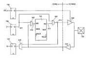
- FIG. 9is a simplified block diagram illustrating FIFO memory 150 as set forth in the present system.
- FIG. 10is a simplified schematic diagram illustrating an input/output (I/O) FIFO control block 114 of the present system.
- FIG. 11is a simplified schematic diagram illustrating RT module, RN module and RO module of the input/output FIFO control block of FIG. 10 .
- FIG. 12is a simplified schematic diagram illustrating RC module of the input/output FIFO control block of FIG. 10 .
- Vccis used to define the positive power supply for the digital circuit as designed.
- the size of a digital circuitmay vary greatly depending on a user's particular circuit requirements.
- Vccmay change depending on the size of the circuit elements used.
- a “signal” as used in this disclosuremay represent the application, or pulling “high” of a voltage to a node in a circuit where there was low or no voltage before, or it may represent the termination, or the bringing “low” of a voltage to the node, depending on the particular implementation of the invention.
- FIG. 3is a block diagram of a core tile 102 in an FPGA 100 of the present system.
- FPGA core tile 102comprises an array of logic clusters 104 , random access memory clusters 106 and random access memory modules 108 .
- Logic clusters 104are connected together by a routing interconnect architecture (not shown) that may comprise multiple levels of routing interconnects.
- FPGA core tile 102is surrounded by input/output (I/O) clusters 110 , input/output (I/O) FIFO control blocks 114 and input/output banks 112 .
- I/O clusters 110There are two rows of I/O clusters 110 on the north and south edges of FPGA 100 and one column of I/O clusters on the west and east edges of FPGA 100 .
- FIG. 4is a block diagram of an FPGA including multiple core tiles 102 as shown as an example in FIG. 3 .
- FPGA 120comprises four core tiles 102 , though other numbers of tiles are possible.
- Core tiles 102are surrounded by I/O clusters 110 , input/output FIFO control blocks 114 and I/O banks 112 .
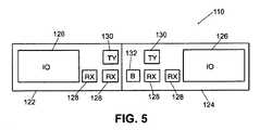
- FIG. 5is a simplified block diagram of a I/O cluster 110 of the present system.
- I/O cluster 110may comprise any number of the logic components indicated below. The example set forth below is for illustrative purposes only and in no way limits the scope of the present invention.
- I/O cluster 110comprises two sub-clusters 122 and 124 .
- Sub-clusters 122 and 124each contain one I/O module 126 , two receiver modules (RX) 128 , and one transmitter module (TY) 130 .
- Sub-cluster 124contains a buffer module 132 .
- receiver modules 128 , transmitter modules 130 and buffer module 132are not described in detail herein.
- the implementation of receiver modules 128 and transmitter modules 130 suitable for use according to the present systemis disclosed in U.S. patent application Ser. No. 10/323,613, filed on Dec. 18, 2002, by inventors Arunangshu Kundu, William C. Plants, John McCollum and Venkatesh Narayanan, entitled “A ROUTING ARCHITECTURE HAVING RECEIVERS AND TRANSMITTERS FOR A FIELD PROGRAMMABLE GATE ARRAY”, and hereby incorporated herein by reference.
- the implementation of buffer modules suitable for use according to the present systemis disclosed in U.S. patent application Ser. No.
- FIG. 6is a simplified schematic diagram illustrating I/O module 126 of the present system and the interface of the I/O module 126 with an I/O pad 132 .
- Each I/O module 126comprises three dedicated registers 152 , 154 , 156 and a 64 bit FIFO 150 .
- I/O modules 126serve two purposes, logic functionality and device protection during programming. The logic functionality depends on the module type. Device protection is needed during programming because the high voltages used to program FPGA 100 's routing interconnect architecture would damage the gate oxide of a standard CMOS gate. I/O modules 126 provide isolation of the programming voltage from the CMOS gates. The protection function will be discussed in greater detail below.
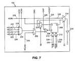
- FIG. 7is a simplified schematic diagram illustrating an input register of the present system.
- register 152comprises a four-input multiplexer 200 having its output coupled to one input of a two-input multiplexer 202 .
- Four-input multiplexer 200selects one input from four clock signal lines 218 , 220 , 222 , 224 .
- Two-input multiplexer 202has a second input coupled to a clock input signal line 225 .
- Two-input multiplexer 202has an output coupled to one input of a two-input XNOR gate 206 .
- Two-input XNOR gate 206has a second input provided from signal line 226 .
- the output of two-input XNOR gate 206is coupled to the clock input of register 208 and provides a clock signal through signal line 234 .
- Signal line 234sends the selected clock signal to FIFO 150 (as shown in FIG. 5 ).
- a second two-input multiplexer 204has one input coupled to signal line 238 and a second input that is looped from the output of register 208 .
- Register 208has a second input coupled to the output of two-input multiplexer 204 and a third and fourth input coupled to signal lines 228 , 230 , 232 , 234 through NAND gates 210 and 212 .
- the output of register 208is coupled to one input of two-input multiplexer 214 .
- the second input of two-input multiplexer 214is from signal line 238 .
- the output of two-input multiplexer 214provides the Y output of register 152 through driver 216 .
- the Y output of register 152may be sent back into the FPGA core logic.
- FIG. 8is a simplified schematic diagram illustrating an output and enable register of the present system.
- Register 154comprises a four-input multiplexer 300 having clock input signals 302 , 304 , 306 , 308 .
- Multiplexer 300has an output coupled to the input of two-input multiplexer 312 .
- Multiplexer 312has a second input coupled to the output of AND gate 310 .
- AND gate 310has two inputs from clock signal lines 314 , 316 .
- the output of multiplexer 312is coupled to one input of a two-input XNOR gate 320 .
- the second input of two-input XNOR 320 gateis coupled to signal line 322 .
- the output of two-input XNOR gateis coupled to the clock input of register 324 and to the selected clock signal output signal line 326 .
- Signal line 326sends the selected clock signal to FIFO 150 (as shown in FIG. 6 ).
- Register 324has a second input coupled to the output of multiplexer 318 and two inputs coupled to the outputs of two-input NAND gates 328 and 330 .
- the output of register 324provides the Y output signal of the register 154 through signal line 338 and through driver 322 .
- the Y output of register 154may be sent back into the FPGA core logic.
- the output of register 324is also coupled to a first input of two-input multiplexer 334 and may also be fed back into the input of register 324 through two-input multiplexer 318 .
- the second input of two input multiplexer 334is coupled to signal line 340 which is coupled to the routing architecture (not shown) of the FPGA.
- the output of multiplexer 334provides the YOUT signal of register 154 through signal line 336 .
- the YOUT signalis sent to either FIFO 150 or I/O pad 132 .
- Register 156is identical to register 154 .
- FIG. 9is another simplified block diagram illustrating FIFO memory 150 as set forth in the present system. For clarity, some of the same reference numerals are used to refer to the same components as used in previous.
- FIFO memory 150has a write data input line 403 coupled to the FPGA core (not shown) through a first input of a first two-input multiplexer 402 and output register 154 . The second input of first two-input multiplexer 402 is coupled to the output of input buffer 416 .
- FIFO memory 150has a read data output line 412 coupled to a first input of a second two-input multiplexer 404 .
- Multiplexer 404has a second input coupled to output signal line 401 of output register 154 and an output coupled to the input of output buffer 406 and to a first input of a third two-input multiplexer 418 .
- Output buffer 406has a control input coupled to the output of enable register 156 and an output coupled to I/O pad 132 .
- I/O pad 132is coupled to the input of input buffer 416 .
- Input buffer 416has an output coupled to a second input of third two-input multiplexer 418 and to a second input of first two-input multiplexer 402 .
- Third two-input multiplexer 418has an output coupled to data input line of input register 152 .
- FIFO memory 150is an 8 word by 8-bit memory array, configured as a 64 by 1 bit memory though other numbers of bits and configurations are possible. FIFO functions are well known to those of ordinary skill in the art and thus the architecture of a FIFO circuit configuration will not be discussed herein to avoid overcomplicating the present disclosure and obscuring the present invention. Two six-bit binary counters are used for generating read and write addresses.
- the input/output FIFO control blocks 114(as shown in FIG. 4 ) provide the FIFO memory 150 with read and write control and standard FIFO flags. Input/output FIFO control blocks 114 will be discussed in greater detail below.
- the standard FIFO flagsare commonly referred to as full, empty, almost full and almost empty flags.
- FIFO 150can be used without input/output FIFO control blocks 114 in applications where flags are not needed. In addition, FIFO 150 can be used without input/output FIFO control blocks 114 in applications where different control logic is needed.
- FIFO 150is functionally inserted into either of the input or output data paths.
- the interface to FIFO 150is determined by a basic three-register I/O structure.
- the present systemallows for the sharing of control signals between registers 152 , 154 , 156 and FIFO 150 .
- the register associated with that data pathprovides the control signal. For example, if FIFO 150 is programmed to buffer the data coming on to the chip, then register 152 would not be used since the data is buffered through FIFO 150 .
- the clock select circuitry of register 152provides the write clock for FIFO 150 via clock output signal line 234 as shown in FIG. 7 .
- register 154if FIFO 150 is programmed to buffer data leaving the chip, register 154 would not be used since the data is buffered through FIFO 150 .
- the clock select circuitry of register 154provides the read clock for FIFO 150 via output signal line 326 as is shown in FIG. 8 .
- FIG. 10is a simplified block diagram illustrating an input/output (I/O) FIFO control block 114 of the present system.
- I/O FIFO control block 114There is a plurality of I/O FIFO control block 114 inserted between I/O clusters 110 along the perimeter of FPGA 100 .
- I/O clusters 110For illustrative purposes only, there are two along each outside edge of each FPGA core tile 102 .
- I/O FIFO control blockcontains a FIFO control block 318 , which contains logic components used to generate the full, empty, almost-full and almost-empty flags, and an I/O FIFO control block cluster 320 .
- FIFO control block 318will not be discussed in detail herein in order to avoid overcomplicating the disclosure and thereby obscuring the present invention.
- Each I/O FIFO control block cluster 320has two sub clusters 300 and 302 .
- Each sub cluster 300 and 302has an RC module 304 , six RT modules 306 , two RN modules 310 , two RO modules 308 a transmitter module 314 and two receiver modules 312 .
- Right sub cluster 302has a buffer module 316 .
- receiver module 312 , transmitter module 314 and buffer modulerelate to the routing architecture of FPGA 100 and will not be discussed herein to avoid overcomplicating and thus obscuring the present disclosure.
- FIG. 11is a simplified schematic diagram illustrating RT module 306 , RN module 310 and RO module 308 of an I/O FIFO control block as shown in FIG. 10 of the present system. Similar reference numbers are used to describe similar elements while new reference numbers are used to describe new components.
- RT module 306comprises a buffer 554 that has an input programmable coupled to a horizontal routing track in routing architecture row 552 .
- Buffer 554has an output that is coupled to FIFO control block 318 .
- RN module 310comprises a two-input AND gate 556 .
- One input of two-input AND gate 556is programmably coupled to a horizontal routing track in routing architecture row 550 .
- the second input of two-input AND gate 556is programmably coupled to a horizontal routing track in routing architecture row 552 .
- the output of two-input AND gate 556is coupled to the input of buffer 358 that has an output that is hardwired to the FIFO control block 318 .
- RO module 308comprises a buffer 560 having an input hardwired to FIFO control block 318 .
- the output of buffer 560drives an output track, which is used- to connect to the programmable routing architecture.
- FIG. 12is a simplified schematic diagram illustrating RC module 304 of I/O FIFO control block 114 as shown in FIG. 10 of the present system.
- RC module 304comprises a four input multiplexer 562 having inputs coupled to the clock network bus 570 (not shown).
- Multiplexer 562has an output coupled to a first input of a two-input multiplexer 565 .
- the second input of two-input multiplexer 565is programmably coupled to the routing architecture in rows 572 and 574 through two-input AND gate 564 .
- Two-input multiplexer 565has an output coupled to an input of a two-input XNOR gate that has a second input programmably coupled to Vcc or ground in routing architecture row 572 .
- the XNOR gate 566is hardwired to FIFO control block RAM 518 through buffer 568 .
- the almost-full and almost-empty flags generated by FIFO control block 114have programmable threshold values.
- the FIFO control block 114performs arithmetic operations on the read and write address to determine when the almost-full and almost-empty conditions are present. Arithmetic logic calculates the difference between the six bit write and read addresses. The magnitude of the difference is compared to the almost full and almost empty threshold values.
Landscapes
- Physics & Mathematics (AREA)
- Mathematical Physics (AREA)
- Engineering & Computer Science (AREA)
- Computer Hardware Design (AREA)
- Computing Systems (AREA)
- General Engineering & Computer Science (AREA)
- Computer Networks & Wireless Communication (AREA)
- Logic Circuits (AREA)
Abstract
Description
Claims (20)
Priority Applications (6)
| Application Number | Priority Date | Filing Date | Title |
|---|---|---|---|
| US10/452,764US6867615B1 (en) | 2003-05-30 | 2003-05-30 | Dedicated input/output first in/first out module for a field programmable gate array |
| US11/056,983US6980028B1 (en) | 2003-05-30 | 2005-02-11 | Dedicated input/output first in/first out module for a field programmable gate array |
| US11/295,889US7102385B2 (en) | 2003-05-30 | 2005-12-06 | Dedicated input/output first in/first out module for a field programmable gate array |
| US11/428,944US7199609B1 (en) | 2003-05-30 | 2006-07-06 | Dedicated input/output first in/first out module for a field programmable gate array |
| US11/677,432US7385419B1 (en) | 2003-05-30 | 2007-02-21 | Dedicated input/output first in/first out module for a field programmable gate array |
| US12/131,722US20080231319A1 (en) | 2003-05-30 | 2008-06-02 | Dedicated input/output first in/first out module for a field programmable gate array |
Applications Claiming Priority (1)
| Application Number | Priority Date | Filing Date | Title |
|---|---|---|---|
| US10/452,764US6867615B1 (en) | 2003-05-30 | 2003-05-30 | Dedicated input/output first in/first out module for a field programmable gate array |
Related Child Applications (1)
| Application Number | Title | Priority Date | Filing Date |
|---|---|---|---|
| US11/056,983ContinuationUS6980028B1 (en) | 2003-05-30 | 2005-02-11 | Dedicated input/output first in/first out module for a field programmable gate array |
Publications (1)
| Publication Number | Publication Date |
|---|---|
| US6867615B1true US6867615B1 (en) | 2005-03-15 |
Family
ID=34272393
Family Applications (3)
| Application Number | Title | Priority Date | Filing Date |
|---|---|---|---|
| US10/452,764Expired - LifetimeUS6867615B1 (en) | 2003-05-30 | 2003-05-30 | Dedicated input/output first in/first out module for a field programmable gate array |
| US11/056,983Expired - LifetimeUS6980028B1 (en) | 2003-05-30 | 2005-02-11 | Dedicated input/output first in/first out module for a field programmable gate array |
| US11/295,889Expired - Fee RelatedUS7102385B2 (en) | 2003-05-30 | 2005-12-06 | Dedicated input/output first in/first out module for a field programmable gate array |
Family Applications After (2)
| Application Number | Title | Priority Date | Filing Date |
|---|---|---|---|
| US11/056,983Expired - LifetimeUS6980028B1 (en) | 2003-05-30 | 2005-02-11 | Dedicated input/output first in/first out module for a field programmable gate array |
| US11/295,889Expired - Fee RelatedUS7102385B2 (en) | 2003-05-30 | 2005-12-06 | Dedicated input/output first in/first out module for a field programmable gate array |
Country Status (1)
| Country | Link |
|---|---|
| US (3) | US6867615B1 (en) |
Cited By (15)
| Publication number | Priority date | Publication date | Assignee | Title |
|---|---|---|---|---|
| US20050036398A1 (en)* | 2003-05-28 | 2005-02-17 | Actel Corporation | Synchronous first-in/first-out block memory for a field programmable gate array |
| US7102385B2 (en) | 2003-05-30 | 2006-09-05 | Actel Corporation | Dedicated input/output first in/first out module for a field programmable gate array |
| US7135887B1 (en)* | 2003-01-07 | 2006-11-14 | Altera Corporation | Programmable logic device multispeed I/O circuitry |
| US7215149B1 (en)* | 2004-12-15 | 2007-05-08 | Lattice Semiconductor Corporation | Interface circuitry for electrical systems |
| US20070236249A1 (en)* | 2006-03-31 | 2007-10-11 | Integrated Device Technology, Inc. | Minimizing timing skew among chip level outputs for registered output signals |
| US20080028354A1 (en)* | 2002-10-08 | 2008-01-31 | Actel Corporation | Parallel programmable antifuse field programmable gate array device (fpga) and a method for programming and testing an antifuse fpga |
| US7385419B1 (en) | 2003-05-30 | 2008-06-10 | Actel Corporation | Dedicated input/output first in/first out module for a field programmable gate array |
| US20080143380A1 (en)* | 2006-12-13 | 2008-06-19 | Fenstermaker Larry R | Low static current drain logic circuit |
| US7560953B1 (en)* | 2008-04-23 | 2009-07-14 | Lattice Semiconductor Corporation | Power management systems and methods for programmable logic devices |
| US7724030B1 (en)* | 2007-12-03 | 2010-05-25 | Xilinx, Inc. | Method and apparatus for providing a feedback path for an output signal |
| US20150162907A1 (en)* | 2013-12-11 | 2015-06-11 | Diehl Aerospace Gmbh | Configurable interface circuit |
| EP3249543A4 (en)* | 2015-07-29 | 2018-04-11 | State Nuclear Power Automation System Engineering | Interface signal remapping method based on fpga |
| US10642541B2 (en)* | 2018-03-08 | 2020-05-05 | quadric.io, Inc. | Machine perception and dense algorithm integrated circuit |
| US10997115B2 (en) | 2018-03-28 | 2021-05-04 | quadric.io, Inc. | Systems and methods for implementing a machine perception and dense algorithm integrated circuit and enabling a flowing propagation of data within the integrated circuit |
| JP2023500300A (en)* | 2019-10-31 | 2023-01-05 | ザイリンクス インコーポレイテッド | programmable device configuration memory system |
Families Citing this family (10)
| Publication number | Priority date | Publication date | Assignee | Title |
|---|---|---|---|---|
| US7631211B1 (en)* | 2006-06-27 | 2009-12-08 | Altera Corporation | Sharing elements in multiple data-rate I/O |
| US7743175B1 (en)* | 2008-07-17 | 2010-06-22 | Xilinx, Inc. | Methods of initializing routing structures in integrated circuits |
| US8358148B1 (en) | 2010-10-01 | 2013-01-22 | Xilinx, Inc. | Programmable integrated circuit and method of asynchronously routing data in an integrated circuit |
| US8913601B1 (en) | 2010-10-01 | 2014-12-16 | Xilinx, Inc. | Programmable integrated circuit and method of asynchronously routing data in a circuit block of an integrated circuit |
| US8294490B1 (en) | 2010-10-01 | 2012-10-23 | Xilinx, Inc. | Integrated circuit and method of asynchronously routing data in an integrated circuit |
| US9780902B2 (en)* | 2011-12-07 | 2017-10-03 | AshRem Technologies, Inc. | Communication systems and methods |
| US11531639B2 (en)* | 2018-07-26 | 2022-12-20 | The Boeing Company | Pipelined cognitive signal processor |
| US11474141B1 (en) | 2019-02-06 | 2022-10-18 | University Of Rhode Island Board Of Trustees | Methods and apparatuses for identifying transmission lines via impedance inhomogeneity patterns |
| WO2021155176A1 (en) | 2020-01-30 | 2021-08-05 | University Of Rhode Island Board Of Trustees | Bus authentication and anti-probing architecture |
| US12306944B1 (en) | 2020-12-29 | 2025-05-20 | University Of Rhode Island Board Of Trustees | Method and apparatus for runtime detection of bus probing/tampering in computer systems |
Citations (117)
| Publication number | Priority date | Publication date | Assignee | Title |
|---|---|---|---|---|
| US4255748A (en) | 1979-02-12 | 1981-03-10 | Automation Systems, Inc. | Bus fault detector |
| US4625313A (en) | 1984-07-06 | 1986-11-25 | Tektronix, Inc. | Method and apparatus for testing electronic equipment |
| US4638187A (en) | 1985-10-01 | 1987-01-20 | Vtc Incorporated | CMOS output buffer providing high drive current with minimum output signal distortion |
| US4638243A (en) | 1985-06-05 | 1987-01-20 | Monolithic Memories, Inc. | Short detector for fusible link array using single reference fuse |
| US4684830A (en) | 1985-03-22 | 1987-08-04 | Monolithic Memories, Inc. | Output circuit for a programmable logic array |
| US4700130A (en) | 1980-03-12 | 1987-10-13 | U.S. Philips Corporation | Current-measuring arrangement with overload protection |
| US4706216A (en) | 1985-02-27 | 1987-11-10 | Xilinx, Inc. | Configurable logic element |
| US4713557A (en) | 1984-09-26 | 1987-12-15 | Xilinx, Inc. | Bidirectional buffer amplifier |
| US4718042A (en) | 1985-12-23 | 1988-01-05 | Ncr Corporation | Non-destructive method and circuit to determine the programmability of a one time programmable device |
| US4717912A (en) | 1982-10-07 | 1988-01-05 | Advanced Micro Devices, Inc. | Apparatus for producing any one of a plurality of signals at a single output |
| US4742252A (en) | 1985-03-29 | 1988-05-03 | Advanced Micro Devices, Inc. | Multiple array customizable logic device |
| US4772812A (en) | 1981-07-27 | 1988-09-20 | Data General Corporation | Tri-state output buffer circuit including a capacitor and dynamic depletion mode switching device |
| US4800176A (en) | 1987-05-29 | 1989-01-24 | Kabushiki Kaisha Toshiba | Method for forming contact portion in semiconductor integrated circuit devices |
| US4857774A (en) | 1986-09-19 | 1989-08-15 | Actel Corporation | Testing apparatus and diagnostic method for use with programmable interconnect architecture |
| US4870302A (en) | 1984-03-12 | 1989-09-26 | Xilinx, Inc. | Configurable electrical circuit having configurable logic elements and configurable interconnects |
| US4870300A (en) | 1986-08-06 | 1989-09-26 | Mitsubishi Denki Kabushiki Kaisha | Standard cell system large scale integrated circuit with heavy load lines passing through the cells |
| US4873459A (en) | 1986-09-19 | 1989-10-10 | Actel Corporation | Programmable interconnect architecture |
| US4928023A (en) | 1987-08-27 | 1990-05-22 | Texas Instruments Incorporated | Improved output buffer having reduced noise characteristics |
| US4930097A (en) | 1988-12-30 | 1990-05-29 | Intel Corporation | Architecture for an improved performance of a programmable logic device |
| US4935645A (en) | 1988-03-02 | 1990-06-19 | Dallas Semiconductor Corporation | Fusing and detection circuit |
| US4959561A (en) | 1989-01-04 | 1990-09-25 | Motorola, Inc. | MOS output buffer with reduced supply line disturbance |
| US4978905A (en) | 1989-10-31 | 1990-12-18 | Cypress Semiconductor Corp. | Noise reduction output buffer |
| EP0415542A2 (en) | 1989-08-15 | 1991-03-06 | Advanced Micro Devices, Inc. | Programmable gate array with improved interconnect structure, input/output structure and configurable logic block |
| US5008855A (en) | 1989-07-18 | 1991-04-16 | Actel Corporation | Method of programming anti-fuse element |
| US5046035A (en) | 1987-08-26 | 1991-09-03 | Ict International Cmos Tech., Inc. | High-performance user programmable logic device (PLD) |
| US5083083A (en) | 1986-09-19 | 1992-01-21 | Actel Corporation | Testability architecture and techniques for programmable interconnect architecture |
| US5121394A (en) | 1989-12-20 | 1992-06-09 | Bull Hn Information Systems Inc. | Method of organizing programmable logic array devices for board testability |
| US5122685A (en) | 1991-03-06 | 1992-06-16 | Quicklogic Corporation | Programmable application specific integrated circuit and logic cell therefor |
| US5126282A (en) | 1990-05-16 | 1992-06-30 | Actel Corporation | Methods of reducing anti-fuse resistance during programming |
| US5132571A (en) | 1990-08-01 | 1992-07-21 | Actel Corporation | Programmable interconnect architecture having interconnects disposed above function modules |
| US5144166A (en) | 1990-11-02 | 1992-09-01 | Concurrent Logic, Inc. | Programmable logic cell and array |
| US5187392A (en) | 1991-07-31 | 1993-02-16 | Intel Corporation | Programmable logic device with limited signal swing |
| US5198705A (en) | 1990-05-11 | 1993-03-30 | Actel Corporation | Logic module with configurable combinational and sequential blocks |
| US5208491A (en) | 1992-01-07 | 1993-05-04 | Washington Research Foundation | Field programmable gate array |
| US5220213A (en) | 1991-03-06 | 1993-06-15 | Quicklogic Corporation | Programmable application specific integrated circuit and logic cell therefor |
| US5220215A (en) | 1992-05-15 | 1993-06-15 | Micron Technology, Inc. | Field programmable logic array with two or planes |
| US5222066A (en) | 1990-12-26 | 1993-06-22 | Motorola, Inc. | Modular self-test for embedded SRAMS |
| US5221865A (en) | 1991-06-21 | 1993-06-22 | Crosspoint Solutions, Inc. | Programmable input/output buffer circuit with test capability |
| US5258319A (en) | 1988-02-19 | 1993-11-02 | Mitsubishi Denki Kabushiki Kaisha | Method of manufacturing a MOS type field effect transistor using an oblique ion implantation step |
| US5272388A (en) | 1992-06-09 | 1993-12-21 | Actel Corporation | High-yield methods for programming antifuses |
| US5286922A (en) | 1992-07-14 | 1994-02-15 | Curtiss Thomas E | Fluorescent coated wire |
| US5293133A (en) | 1992-08-27 | 1994-03-08 | Quicklogic Corporation | Method of determining an electrical characteristic of an antifuse and apparatus therefor |
| US5300832A (en) | 1992-11-10 | 1994-04-05 | Sun Microsystems, Inc. | Voltage interfacing buffer with isolation transistors used for overvoltage protection |
| US5300830A (en) | 1992-05-15 | 1994-04-05 | Micron Semiconductor, Inc. | Programmable logic device macrocell with an exclusive feedback and exclusive external input lines for registered and combinatorial modes using a dedicated product term for control |
| US5317698A (en) | 1992-08-18 | 1994-05-31 | Actel Corporation | FPGA architecture including direct logic function circuit to I/O interconnections |
| US5365485A (en) | 1993-11-22 | 1994-11-15 | Texas Instruments Incorporated | Fifo with fast retransmit mode |
| US5367207A (en) | 1990-12-04 | 1994-11-22 | Xilinx, Inc. | Structure and method for programming antifuses in an integrated circuit array |
| US5375089A (en) | 1993-10-05 | 1994-12-20 | Advanced Micro Devices, Inc. | Plural port memory system utilizing a memory having a read port and a write port |
| US5394034A (en) | 1992-07-27 | 1995-02-28 | Siemens Aktiengesellschaft | Programmable logic array having programmable output driver drive capacity |
| US5394033A (en) | 1993-09-01 | 1995-02-28 | Lattice Semiconductor Corporation | Structure and method for implementing hierarchical routing pools in a programmable logic circuit |
| US5396128A (en) | 1993-09-13 | 1995-03-07 | Motorola, Inc. | Output circuit for interfacing integrated circuits having different power supply potentials |
| US5397939A (en) | 1991-07-31 | 1995-03-14 | Quicklogic Corporation | Programming of antifuses |
| US5400262A (en) | 1989-09-20 | 1995-03-21 | Aptix Corporation | Universal interconnect matrix array |
| US5399920A (en) | 1993-11-09 | 1995-03-21 | Texas Instruments Incorporated | CMOS driver which uses a higher voltage to compensate for threshold loss of the pull-up NFET |
| US5430335A (en) | 1991-05-15 | 1995-07-04 | Oki Electric Industry Co., Ltd. | Simplified low-noise output buffer circuit |
| US5430687A (en) | 1994-04-01 | 1995-07-04 | Xilinx, Inc. | Programmable logic device including a parallel input device for loading memory cells |
| US5469003A (en) | 1992-11-05 | 1995-11-21 | Xilinx, Inc. | Hierarchically connectable configurable cellular array |
| US5469396A (en) | 1994-06-07 | 1995-11-21 | Actel Corporation | Apparatus and method determining the resistance of antifuses in an array |
| US5473268A (en) | 1992-05-18 | 1995-12-05 | Ecole Polytechnique Federale De Lausanne | Intermediary circuit between a low voltage logic circuit and a high voltage output stage in standard CMOS technology |
| US5485103A (en) | 1991-09-03 | 1996-01-16 | Altera Corporation | Programmable logic array with local and global conductors |
| US5486775A (en) | 1993-11-22 | 1996-01-23 | Altera Corporation | Multiplexer structures for use in making controllable interconnections in integrated circuits. |
| US5537057A (en) | 1995-02-14 | 1996-07-16 | Altera Corporation | Programmable logic array device with grouped logic regions and three types of conductors |
| US5546019A (en) | 1995-08-24 | 1996-08-13 | Taiwan Semiconductor Manufacture Company | CMOS I/O circuit with 3.3 volt output and tolerance of 5 volt input |
| US5559464A (en) | 1993-07-06 | 1996-09-24 | Seiko Epson Corporation | Signal voltage level conversion circuit and output buffer circuit |
| US5572148A (en)* | 1995-03-22 | 1996-11-05 | Altera Corporation | Programmable logic array integrated circuit with general-purpose memory configurable as a random access or FIFO memory |
| US5666322A (en) | 1995-09-21 | 1997-09-09 | Nec Electronics, Inc. | Phase-locked loop timing controller in an integrated circuit memory |
| US5670905A (en) | 1994-07-20 | 1997-09-23 | Micron Technology, Inc. | Low-to-high voltage CMOS driver circuit for driving capacitive loads |
| US5744979A (en) | 1992-07-23 | 1998-04-28 | Xilinx, Inc. | FPGA having logic cells configured by SRAM memory cells and interconnect configured by antifuses |
| US5744980A (en) | 1996-02-16 | 1998-04-28 | Actel Corporation | Flexible, high-performance static RAM architecture for field-programmable gate arrays |
| US5801547A (en) | 1996-03-01 | 1998-09-01 | Xilinx, Inc. | Embedded memory for field programmable gate array |
| US5809281A (en) | 1993-03-30 | 1998-09-15 | Altera Corporation | Field programmable gate array with high speed SRAM based configurable function block configurable as high performance logic or block of SRAM |
| US5815003A (en) | 1994-11-04 | 1998-09-29 | Altera Corporation | Programmable logic integrated circuits with partitioned logic element using shared lab-wide signals |
| US5815004A (en) | 1995-10-16 | 1998-09-29 | Xilinx, Inc. | Multi-buffered configurable logic block output lines in a field programmable gate array |
| US5821776A (en) | 1997-01-31 | 1998-10-13 | Actel Corporation | Field programmable gate array with mask programmed analog function circuits |
| US5825662A (en) | 1995-08-18 | 1998-10-20 | Xilinx, Inc. | Computer-implemented method of optimizing a time multiplexed programmable logic device |
| US5825200A (en) | 1996-06-21 | 1998-10-20 | Quicklogic Corporation | Programming architecture for a programmable integrated circuit employing antifuses |
| US5825202A (en) | 1996-09-26 | 1998-10-20 | Xilinx, Inc. | Integrated circuit with field programmable and application specific logic areas |
| US5828538A (en) | 1996-06-21 | 1998-10-27 | Quicklogic Corporation | Power-up circuit for field programmable gate arrays |
| US5828230A (en) | 1997-01-09 | 1998-10-27 | Xilinx, Inc. | FPGA two turn routing structure with lane changing and minimum diffusion area |
| US5835165A (en) | 1995-06-07 | 1998-11-10 | Lsi Logic Corporation | Reduction of false locking code words in concatenated decoders |
| US5832892A (en) | 1996-10-11 | 1998-11-10 | Yaoita; Yasuhito | Spark ignition internal combustion engine |
| US5835998A (en) | 1996-04-04 | 1998-11-10 | Altera Corporation | Logic cell for programmable logic devices |
| US5838167A (en) | 1995-05-26 | 1998-11-17 | Xilinx, Inc. | Method and structure for loading data into several IC devices |
| US5838584A (en) | 1995-01-27 | 1998-11-17 | Altera Corporation | Optimizing chain placement in a programmable logic device |
| US5838954A (en) | 1995-08-18 | 1998-11-17 | Xilinx, Inc. | Computer-implemented method of optimizing a time multiplexed programmable logic device |
| US5848006A (en) | 1995-12-06 | 1998-12-08 | Nec Corporation | Redundant semiconductor memory device using a single now address decoder for driving both sub-wordlines and redundant sub-wordlines |
| US5848005A (en) | 1991-09-03 | 1998-12-08 | Altera Corporation | Programmable logic array integrated circuits |
| US5847441A (en) | 1996-05-10 | 1998-12-08 | Micron Technology, Inc. | Semiconductor junction antifuse circuit |
| US5847577A (en) | 1995-02-24 | 1998-12-08 | Xilinx, Inc. | DRAM memory cell for programmable logic devices |
| US5850152A (en) | 1995-05-17 | 1998-12-15 | Altera Corporation | Programmable logic array integrated circuit devices |
| US5850564A (en) | 1995-05-03 | 1998-12-15 | Btr, Inc, | Scalable multiple level tab oriented interconnect architecture |
| US5852608A (en) | 1996-06-06 | 1998-12-22 | Sun Microsystems, Inc. | Structure and method for bi-directional data transfer between asynchronous clock domains |
| US5854763A (en) | 1997-01-31 | 1998-12-29 | Mosaid Technologies Inc. | Integrated circuit with non-binary decoding and data access |
| EP0889593A1 (en) | 1994-05-19 | 1999-01-07 | Actel Corporation | Programmable logic module for field programmable gate array device |
| US5859544A (en) | 1996-09-05 | 1999-01-12 | Altera Corporation | Dynamic configurable elements for programmable logic devices |
| US5870586A (en) | 1996-01-31 | 1999-02-09 | Xilinx, Inc. | Configuration emulation of a programmable logic device |
| US5869981A (en) | 1985-03-29 | 1999-02-09 | Advanced Micro Devices, Inc. | High density programmable logic device |
| US5880512A (en) | 1991-04-26 | 1999-03-09 | Quicklogic Corporation | Programmable interconnect structures and programmable integrated circuits |
| US5880492A (en) | 1995-10-16 | 1999-03-09 | Xilinx, Inc. | Dedicated local line interconnect layout |
| US5880597A (en) | 1996-09-18 | 1999-03-09 | Altera Corporation | Interleaved interconnect for programmable logic array devices |
| US5880598A (en) | 1997-01-10 | 1999-03-09 | Xilinx, Inc. | Tile-based modular routing resources for high density programmable logic device |
| US5883850A (en) | 1991-09-03 | 1999-03-16 | Altera Corporation | Programmable logic array integrated circuits |
| US5883526A (en) | 1997-04-17 | 1999-03-16 | Altera Corporation | Hierarchical interconnect for programmable logic devices |
| US5949719A (en) | 1995-12-20 | 1999-09-07 | International Business Machines Corporation | Field programmable memory array |
| US5952847A (en) | 1996-06-25 | 1999-09-14 | Actel Corporation | Multiple logic family compatible output driver |
| US5994934A (en) | 1998-01-13 | 1999-11-30 | Mitsubishi Denki Kabushiki Kaisha | Delay locked loop circuit |
| US6011744A (en) | 1997-07-16 | 2000-01-04 | Altera Corporation | Programmable logic device with multi-port memory |
| US6034677A (en) | 1997-10-17 | 2000-03-07 | Sony Corporation | Method and apparatus for displaying an electronic program guide |
| US6038627A (en) | 1998-03-16 | 2000-03-14 | Actel Corporation | SRAM bus architecture and interconnect to an FPGA |
| US6049487A (en) | 1998-03-16 | 2000-04-11 | Actel Corporation | Embedded static random access memory for field programmable gate array |
| US6111448A (en) | 1997-09-10 | 2000-08-29 | Nec Corporation | Clock signal distribution circuit |
| US6181174B1 (en) | 1998-09-24 | 2001-01-30 | Fujitsu Limited | Semiconductor integrated circuit device |
| US6289068B1 (en) | 1998-06-22 | 2001-09-11 | Xilinx, Inc. | Delay lock loop with clock phase shifter |
| US6292016B1 (en) | 1995-10-16 | 2001-09-18 | Altera Corporation | Programmable logic with on-chip DLL or PLL to distribute clock |
| EP1137188A2 (en) | 2000-03-24 | 2001-09-26 | STMicroelectronics, Inc. | Digital phase lock loop |
| US6329839B1 (en) | 1996-09-04 | 2001-12-11 | Advantage Logic, Inc. | Method and apparatus for universal program controlled bus architecture |
| US6437650B1 (en) | 1999-01-08 | 2002-08-20 | Altera Corporation | Phase-locked loop or delay-locked loop circuitry for programmable logic devices |
Family Cites Families (7)
| Publication number | Priority date | Publication date | Assignee | Title |
|---|---|---|---|---|
| US5286992A (en) | 1990-09-28 | 1994-02-15 | Actel Corporation | Low voltage device in a high voltage substrate |
| US6127865A (en) | 1997-05-23 | 2000-10-03 | Altera Corporation | Programmable logic device with logic signal delay compensated clock network |
| US6107826A (en) | 1998-08-19 | 2000-08-22 | Xilinx, Inc. | Interconnect structure for FPGA with configurable delay locked loop |
| US6751723B1 (en)* | 2000-09-02 | 2004-06-15 | Actel Corporation | Field programmable gate array and microcontroller system-on-a-chip |
| US6727726B1 (en) | 2002-11-12 | 2004-04-27 | Actel Corporation | Field programmable gate array architecture including a buffer module and a method of distributing buffer modules in a field programmable gate array |
| US6946871B1 (en) | 2002-12-18 | 2005-09-20 | Actel Corporation | Multi-level routing architecture in a field programmable gate array having transmitters and receivers |
| US6867615B1 (en) | 2003-05-30 | 2005-03-15 | Actel Corporation | Dedicated input/output first in/first out module for a field programmable gate array |
- 2003
- 2003-05-30USUS10/452,764patent/US6867615B1/ennot_activeExpired - Lifetime
- 2005
- 2005-02-11USUS11/056,983patent/US6980028B1/ennot_activeExpired - Lifetime
- 2005-12-06USUS11/295,889patent/US7102385B2/ennot_activeExpired - Fee Related
Patent Citations (130)
| Publication number | Priority date | Publication date | Assignee | Title |
|---|---|---|---|---|
| US4255748A (en) | 1979-02-12 | 1981-03-10 | Automation Systems, Inc. | Bus fault detector |
| US4700130A (en) | 1980-03-12 | 1987-10-13 | U.S. Philips Corporation | Current-measuring arrangement with overload protection |
| US4772812A (en) | 1981-07-27 | 1988-09-20 | Data General Corporation | Tri-state output buffer circuit including a capacitor and dynamic depletion mode switching device |
| US4717912A (en) | 1982-10-07 | 1988-01-05 | Advanced Micro Devices, Inc. | Apparatus for producing any one of a plurality of signals at a single output |
| US4870302A (en) | 1984-03-12 | 1989-09-26 | Xilinx, Inc. | Configurable electrical circuit having configurable logic elements and configurable interconnects |
| US4625313A (en) | 1984-07-06 | 1986-11-25 | Tektronix, Inc. | Method and apparatus for testing electronic equipment |
| US4713557A (en) | 1984-09-26 | 1987-12-15 | Xilinx, Inc. | Bidirectional buffer amplifier |
| US4706216A (en) | 1985-02-27 | 1987-11-10 | Xilinx, Inc. | Configurable logic element |
| US4684830A (en) | 1985-03-22 | 1987-08-04 | Monolithic Memories, Inc. | Output circuit for a programmable logic array |
| US5869981A (en) | 1985-03-29 | 1999-02-09 | Advanced Micro Devices, Inc. | High density programmable logic device |
| US4742252A (en) | 1985-03-29 | 1988-05-03 | Advanced Micro Devices, Inc. | Multiple array customizable logic device |
| US4638243A (en) | 1985-06-05 | 1987-01-20 | Monolithic Memories, Inc. | Short detector for fusible link array using single reference fuse |
| US4638187B1 (en) | 1985-10-01 | 1993-03-02 | Cypress Semiconductor Minnesot | |
| US4638187A (en) | 1985-10-01 | 1987-01-20 | Vtc Incorporated | CMOS output buffer providing high drive current with minimum output signal distortion |
| US4718042A (en) | 1985-12-23 | 1988-01-05 | Ncr Corporation | Non-destructive method and circuit to determine the programmability of a one time programmable device |
| US4870300A (en) | 1986-08-06 | 1989-09-26 | Mitsubishi Denki Kabushiki Kaisha | Standard cell system large scale integrated circuit with heavy load lines passing through the cells |
| US4873459A (en) | 1986-09-19 | 1989-10-10 | Actel Corporation | Programmable interconnect architecture |
| US4857774A (en) | 1986-09-19 | 1989-08-15 | Actel Corporation | Testing apparatus and diagnostic method for use with programmable interconnect architecture |
| US5083083A (en) | 1986-09-19 | 1992-01-21 | Actel Corporation | Testability architecture and techniques for programmable interconnect architecture |
| US4873459B1 (en) | 1986-09-19 | 1995-01-10 | Actel Corp | Programmable interconnect architecture |
| US4800176A (en) | 1987-05-29 | 1989-01-24 | Kabushiki Kaisha Toshiba | Method for forming contact portion in semiconductor integrated circuit devices |
| US5046035A (en) | 1987-08-26 | 1991-09-03 | Ict International Cmos Tech., Inc. | High-performance user programmable logic device (PLD) |
| US4928023A (en) | 1987-08-27 | 1990-05-22 | Texas Instruments Incorporated | Improved output buffer having reduced noise characteristics |
| US5258319A (en) | 1988-02-19 | 1993-11-02 | Mitsubishi Denki Kabushiki Kaisha | Method of manufacturing a MOS type field effect transistor using an oblique ion implantation step |
| US4935645A (en) | 1988-03-02 | 1990-06-19 | Dallas Semiconductor Corporation | Fusing and detection circuit |
| US4930097A (en) | 1988-12-30 | 1990-05-29 | Intel Corporation | Architecture for an improved performance of a programmable logic device |
| US4959561A (en) | 1989-01-04 | 1990-09-25 | Motorola, Inc. | MOS output buffer with reduced supply line disturbance |
| US5008855A (en) | 1989-07-18 | 1991-04-16 | Actel Corporation | Method of programming anti-fuse element |
| EP0415542A3 (en) | 1989-08-15 | 1991-10-02 | Advanced Micro Devices, Inc. | Programmable gate array with improved interconnect structure, input/output structure and configurable logic block |
| EP0415542A2 (en) | 1989-08-15 | 1991-03-06 | Advanced Micro Devices, Inc. | Programmable gate array with improved interconnect structure, input/output structure and configurable logic block |
| US5400262A (en) | 1989-09-20 | 1995-03-21 | Aptix Corporation | Universal interconnect matrix array |
| US4978905A (en) | 1989-10-31 | 1990-12-18 | Cypress Semiconductor Corp. | Noise reduction output buffer |
| US5121394A (en) | 1989-12-20 | 1992-06-09 | Bull Hn Information Systems Inc. | Method of organizing programmable logic array devices for board testability |
| US5198705A (en) | 1990-05-11 | 1993-03-30 | Actel Corporation | Logic module with configurable combinational and sequential blocks |
| US5126282A (en) | 1990-05-16 | 1992-06-30 | Actel Corporation | Methods of reducing anti-fuse resistance during programming |
| US5132571A (en) | 1990-08-01 | 1992-07-21 | Actel Corporation | Programmable interconnect architecture having interconnects disposed above function modules |
| US5144166A (en) | 1990-11-02 | 1992-09-01 | Concurrent Logic, Inc. | Programmable logic cell and array |
| US5367207A (en) | 1990-12-04 | 1994-11-22 | Xilinx, Inc. | Structure and method for programming antifuses in an integrated circuit array |
| US5222066A (en) | 1990-12-26 | 1993-06-22 | Motorola, Inc. | Modular self-test for embedded SRAMS |
| US5220213A (en) | 1991-03-06 | 1993-06-15 | Quicklogic Corporation | Programmable application specific integrated circuit and logic cell therefor |
| US5122685A (en) | 1991-03-06 | 1992-06-16 | Quicklogic Corporation | Programmable application specific integrated circuit and logic cell therefor |
| US5880512A (en) | 1991-04-26 | 1999-03-09 | Quicklogic Corporation | Programmable interconnect structures and programmable integrated circuits |
| US5430335A (en) | 1991-05-15 | 1995-07-04 | Oki Electric Industry Co., Ltd. | Simplified low-noise output buffer circuit |
| US5221865A (en) | 1991-06-21 | 1993-06-22 | Crosspoint Solutions, Inc. | Programmable input/output buffer circuit with test capability |
| US5397939A (en) | 1991-07-31 | 1995-03-14 | Quicklogic Corporation | Programming of antifuses |
| US5187392A (en) | 1991-07-31 | 1993-02-16 | Intel Corporation | Programmable logic device with limited signal swing |
| US5485103A (en) | 1991-09-03 | 1996-01-16 | Altera Corporation | Programmable logic array with local and global conductors |
| US5848005A (en) | 1991-09-03 | 1998-12-08 | Altera Corporation | Programmable logic array integrated circuits |
| US5883850A (en) | 1991-09-03 | 1999-03-16 | Altera Corporation | Programmable logic array integrated circuits |
| US5208491A (en) | 1992-01-07 | 1993-05-04 | Washington Research Foundation | Field programmable gate array |
| US5220215A (en) | 1992-05-15 | 1993-06-15 | Micron Technology, Inc. | Field programmable logic array with two or planes |
| US5300830A (en) | 1992-05-15 | 1994-04-05 | Micron Semiconductor, Inc. | Programmable logic device macrocell with an exclusive feedback and exclusive external input lines for registered and combinatorial modes using a dedicated product term for control |
| US5473268A (en) | 1992-05-18 | 1995-12-05 | Ecole Polytechnique Federale De Lausanne | Intermediary circuit between a low voltage logic circuit and a high voltage output stage in standard CMOS technology |
| US5272388A (en) | 1992-06-09 | 1993-12-21 | Actel Corporation | High-yield methods for programming antifuses |
| US5286922A (en) | 1992-07-14 | 1994-02-15 | Curtiss Thomas E | Fluorescent coated wire |
| US5744979A (en) | 1992-07-23 | 1998-04-28 | Xilinx, Inc. | FPGA having logic cells configured by SRAM memory cells and interconnect configured by antifuses |
| US5394034A (en) | 1992-07-27 | 1995-02-28 | Siemens Aktiengesellschaft | Programmable logic array having programmable output driver drive capacity |
| US5317698A (en) | 1992-08-18 | 1994-05-31 | Actel Corporation | FPGA architecture including direct logic function circuit to I/O interconnections |
| US5293133A (en) | 1992-08-27 | 1994-03-08 | Quicklogic Corporation | Method of determining an electrical characteristic of an antifuse and apparatus therefor |
| US5469003A (en) | 1992-11-05 | 1995-11-21 | Xilinx, Inc. | Hierarchically connectable configurable cellular array |
| US5831448A (en) | 1992-11-05 | 1998-11-03 | Xilinx, Inc. | Function unit for fine-gained FPGA |
| US5861761A (en) | 1992-11-05 | 1999-01-19 | Xilinx, Inc. | Hierarchically connectable configurable cellular array |
| US5300832A (en) | 1992-11-10 | 1994-04-05 | Sun Microsystems, Inc. | Voltage interfacing buffer with isolation transistors used for overvoltage protection |
| US5809281A (en) | 1993-03-30 | 1998-09-15 | Altera Corporation | Field programmable gate array with high speed SRAM based configurable function block configurable as high performance logic or block of SRAM |
| US5559464A (en) | 1993-07-06 | 1996-09-24 | Seiko Epson Corporation | Signal voltage level conversion circuit and output buffer circuit |
| US5394033A (en) | 1993-09-01 | 1995-02-28 | Lattice Semiconductor Corporation | Structure and method for implementing hierarchical routing pools in a programmable logic circuit |
| US5396128A (en) | 1993-09-13 | 1995-03-07 | Motorola, Inc. | Output circuit for interfacing integrated circuits having different power supply potentials |
| US5375089A (en) | 1993-10-05 | 1994-12-20 | Advanced Micro Devices, Inc. | Plural port memory system utilizing a memory having a read port and a write port |
| US5399920A (en) | 1993-11-09 | 1995-03-21 | Texas Instruments Incorporated | CMOS driver which uses a higher voltage to compensate for threshold loss of the pull-up NFET |
| US5486775A (en) | 1993-11-22 | 1996-01-23 | Altera Corporation | Multiplexer structures for use in making controllable interconnections in integrated circuits. |
| US5365485A (en) | 1993-11-22 | 1994-11-15 | Texas Instruments Incorporated | Fifo with fast retransmit mode |
| US5430687A (en) | 1994-04-01 | 1995-07-04 | Xilinx, Inc. | Programmable logic device including a parallel input device for loading memory cells |
| EP0889593A1 (en) | 1994-05-19 | 1999-01-07 | Actel Corporation | Programmable logic module for field programmable gate array device |
| US5526312A (en) | 1994-06-07 | 1996-06-11 | Actel Corporation | Apparatus and method for determining the resistance of antifuses in an array |
| US5469396A (en) | 1994-06-07 | 1995-11-21 | Actel Corporation | Apparatus and method determining the resistance of antifuses in an array |
| US5572476A (en) | 1994-06-07 | 1996-11-05 | Actel Corporation | Apparatus and method for determining the resistance of antifuses in an array |
| US5670905A (en) | 1994-07-20 | 1997-09-23 | Micron Technology, Inc. | Low-to-high voltage CMOS driver circuit for driving capacitive loads |
| US5815003A (en) | 1994-11-04 | 1998-09-29 | Altera Corporation | Programmable logic integrated circuits with partitioned logic element using shared lab-wide signals |
| US5859542A (en) | 1994-11-04 | 1999-01-12 | Altera Corporation | Programmable logic array integrated circuits with enhanced cascade |
| US5838584A (en) | 1995-01-27 | 1998-11-17 | Altera Corporation | Optimizing chain placement in a programmable logic device |
| US5537057A (en) | 1995-02-14 | 1996-07-16 | Altera Corporation | Programmable logic array device with grouped logic regions and three types of conductors |
| US5847577A (en) | 1995-02-24 | 1998-12-08 | Xilinx, Inc. | DRAM memory cell for programmable logic devices |
| US5572148A (en)* | 1995-03-22 | 1996-11-05 | Altera Corporation | Programmable logic array integrated circuit with general-purpose memory configurable as a random access or FIFO memory |
| US5850564A (en) | 1995-05-03 | 1998-12-15 | Btr, Inc, | Scalable multiple level tab oriented interconnect architecture |
| US5850151A (en)* | 1995-05-17 | 1998-12-15 | Altera Corporation | Programmable logic array intergrated circuit devices |
| US5850152A (en) | 1995-05-17 | 1998-12-15 | Altera Corporation | Programmable logic array integrated circuit devices |
| US5838167A (en) | 1995-05-26 | 1998-11-17 | Xilinx, Inc. | Method and structure for loading data into several IC devices |
| US5835165A (en) | 1995-06-07 | 1998-11-10 | Lsi Logic Corporation | Reduction of false locking code words in concatenated decoders |
| US5825662A (en) | 1995-08-18 | 1998-10-20 | Xilinx, Inc. | Computer-implemented method of optimizing a time multiplexed programmable logic device |
| US5838954A (en) | 1995-08-18 | 1998-11-17 | Xilinx, Inc. | Computer-implemented method of optimizing a time multiplexed programmable logic device |
| US5546019A (en) | 1995-08-24 | 1996-08-13 | Taiwan Semiconductor Manufacture Company | CMOS I/O circuit with 3.3 volt output and tolerance of 5 volt input |
| US5666322A (en) | 1995-09-21 | 1997-09-09 | Nec Electronics, Inc. | Phase-locked loop timing controller in an integrated circuit memory |
| US5815004A (en) | 1995-10-16 | 1998-09-29 | Xilinx, Inc. | Multi-buffered configurable logic block output lines in a field programmable gate array |
| US6292016B1 (en) | 1995-10-16 | 2001-09-18 | Altera Corporation | Programmable logic with on-chip DLL or PLL to distribute clock |
| US5880492A (en) | 1995-10-16 | 1999-03-09 | Xilinx, Inc. | Dedicated local line interconnect layout |
| US5848006A (en) | 1995-12-06 | 1998-12-08 | Nec Corporation | Redundant semiconductor memory device using a single now address decoder for driving both sub-wordlines and redundant sub-wordlines |
| US5949719A (en) | 1995-12-20 | 1999-09-07 | International Business Machines Corporation | Field programmable memory array |
| US5870586A (en) | 1996-01-31 | 1999-02-09 | Xilinx, Inc. | Configuration emulation of a programmable logic device |
| US5744980A (en) | 1996-02-16 | 1998-04-28 | Actel Corporation | Flexible, high-performance static RAM architecture for field-programmable gate arrays |
| US5801547A (en) | 1996-03-01 | 1998-09-01 | Xilinx, Inc. | Embedded memory for field programmable gate array |
| US5835998A (en) | 1996-04-04 | 1998-11-10 | Altera Corporation | Logic cell for programmable logic devices |
| US5847441A (en) | 1996-05-10 | 1998-12-08 | Micron Technology, Inc. | Semiconductor junction antifuse circuit |
| US5852608A (en) | 1996-06-06 | 1998-12-22 | Sun Microsystems, Inc. | Structure and method for bi-directional data transfer between asynchronous clock domains |
| US5859543A (en) | 1996-06-21 | 1999-01-12 | Quicklogic Corporation | Programming architecture for a programmable integrated circuit employing antifuses |
| US5825201A (en) | 1996-06-21 | 1998-10-20 | Quicklogic Corporation | Programming architecture for a programmable integrated circuit employing antifuses |
| US5825200A (en) | 1996-06-21 | 1998-10-20 | Quicklogic Corporation | Programming architecture for a programmable integrated circuit employing antifuses |
| US5828538A (en) | 1996-06-21 | 1998-10-27 | Quicklogic Corporation | Power-up circuit for field programmable gate arrays |
| US5952847A (en) | 1996-06-25 | 1999-09-14 | Actel Corporation | Multiple logic family compatible output driver |
| US6329839B1 (en) | 1996-09-04 | 2001-12-11 | Advantage Logic, Inc. | Method and apparatus for universal program controlled bus architecture |
| US5859544A (en) | 1996-09-05 | 1999-01-12 | Altera Corporation | Dynamic configurable elements for programmable logic devices |
| US5880597A (en) | 1996-09-18 | 1999-03-09 | Altera Corporation | Interleaved interconnect for programmable logic array devices |
| US5825202A (en) | 1996-09-26 | 1998-10-20 | Xilinx, Inc. | Integrated circuit with field programmable and application specific logic areas |
| US5832892A (en) | 1996-10-11 | 1998-11-10 | Yaoita; Yasuhito | Spark ignition internal combustion engine |
| US5828230A (en) | 1997-01-09 | 1998-10-27 | Xilinx, Inc. | FPGA two turn routing structure with lane changing and minimum diffusion area |
| US5880598A (en) | 1997-01-10 | 1999-03-09 | Xilinx, Inc. | Tile-based modular routing resources for high density programmable logic device |
| US5854763A (en) | 1997-01-31 | 1998-12-29 | Mosaid Technologies Inc. | Integrated circuit with non-binary decoding and data access |
| US5821776A (en) | 1997-01-31 | 1998-10-13 | Actel Corporation | Field programmable gate array with mask programmed analog function circuits |
| US5883526A (en) | 1997-04-17 | 1999-03-16 | Altera Corporation | Hierarchical interconnect for programmable logic devices |
| US6011744A (en) | 1997-07-16 | 2000-01-04 | Altera Corporation | Programmable logic device with multi-port memory |
| US6111448A (en) | 1997-09-10 | 2000-08-29 | Nec Corporation | Clock signal distribution circuit |
| US6034677A (en) | 1997-10-17 | 2000-03-07 | Sony Corporation | Method and apparatus for displaying an electronic program guide |
| US5994934A (en) | 1998-01-13 | 1999-11-30 | Mitsubishi Denki Kabushiki Kaisha | Delay locked loop circuit |
| US6049487A (en) | 1998-03-16 | 2000-04-11 | Actel Corporation | Embedded static random access memory for field programmable gate array |
| US6038627A (en) | 1998-03-16 | 2000-03-14 | Actel Corporation | SRAM bus architecture and interconnect to an FPGA |
| US6430088B1 (en) | 1998-03-16 | 2002-08-06 | Actel Corporation | Embedded static random access memory for field programmable gate array |
| US6496887B1 (en) | 1998-03-16 | 2002-12-17 | Actel Corporation | SRAM bus architecture and interconnect to an FPGA |
| US6289068B1 (en) | 1998-06-22 | 2001-09-11 | Xilinx, Inc. | Delay lock loop with clock phase shifter |
| US6181174B1 (en) | 1998-09-24 | 2001-01-30 | Fujitsu Limited | Semiconductor integrated circuit device |
| US6437650B1 (en) | 1999-01-08 | 2002-08-20 | Altera Corporation | Phase-locked loop or delay-locked loop circuitry for programmable logic devices |
| EP1137188A2 (en) | 2000-03-24 | 2001-09-26 | STMicroelectronics, Inc. | Digital phase lock loop |
Non-Patent Citations (18)
| Title |
|---|
| "APEX 20KC Programmable Logic Device", Altera Corp. DS-APEX20KC-2.1 Data Sheet, pp. 1-87, Apr. 2002. |
| "AV9170 Application Note", AvaSem, pp. 1-7, Jan. 1993. |
| "AV9170 Clock Synchronizer and Multiplier", pp. 1-4, 8, Nov. 1992. |
| "Introduction to Actel FPGA Architecture", Actel Corp. Application Note, pp. 5-1-5-8, Sep. 1997. |
| "Virtex(TM)-E 1.8 V Field Programmable Gate Arrays", Xilinx Corp. Production Product Specification, Module 1, DS022-1 (v2.3) pp. 1-6, Module 2, DS022-2 (v2.4) pp. 1-52, Module 3, DS022-3 (v2.8) pp. 1-25, and Module 4, DS022-4 (v2.4) pp. 1-147, Jul. 17, 2002. |
| "Virtex(TM)-II Platform FPGAs", Xilinx Corp. Advance Product Specification DS031, 315 pages total, Module 1 published Sep. 26, 2002, Modules 2, 3, & 4 published May 7, 2003. |
| "XC4000E and XC4000X Series Field Programmable Gate Arrays", Xilinx Corp. Product Specification (Version 1.6), pp. 6-5-6-72, May 14, 1999. |
| "Virtex™-E 1.8 V Field Programmable Gate Arrays", Xilinx Corp. Production Product Specification, Module 1, DS022-1 (v2.3) pp. 1-6, Module 2, DS022-2 (v2.4) pp. 1-52, Module 3, DS022-3 (v2.8) pp. 1-25, and Module 4, DS022-4 (v2.4) pp. 1-147, Jul. 17, 2002. |
| "Virtex™-II Platform FPGAs", Xilinx Corp. Advance Product Specification DS031, 315 pages total, Module 1 published Sep. 26, 2002, Modules 2, 3, & 4 published May 7, 2003. |
| A. Efendovich et al., "Multi-Frequency Zero-Jitter Delay-Locked Loop", IEEE 1993 Custom Integrated Circuits Conference, pp. 27.1.1-27.1.4, Conf. Date: May 9-12, 1993. |
| D. Bursky, "Memories Hit New Highs And Clocks Run Jitter-Free", Electronic Design, pp. 79-80, 84-85, 89-93, Feb. 19, 1996. |
| J. Chen, "PLL-based clock systems span the system spectrum from green PCS to Alpha", EDN, pp. 147-148, 150, 152, 154-155, Nov. 9, 1995. |
| L. Ashby, "ASIC Clock Distribution using a Phase Locked Loop (PLL)", Proceedings Fourth Annual IEEE International ASIC Conference and Exhibit, pp. 6.1-6.3, Sep. 1991. |
| P. Sevalia, "Straightforward techniques cut jitter in PLL-based clock drivers", EDN, pp. 119-123, 125, Nov. 23, 1995. |
| R. Quinnell, "Blending gate arrays with dedicated circuits sweetens ASIC development", EDN, pp. 29-32, Mar. 31, 1994. |
| U. Ko, "A 30-ps JITTER, 3.6-mus Locking, 3.3-Volt digital PLL for CMOS Gate Arrays", IEEE 1993 Custom Integrated Circuits Conference, pp. 23.3.1-23.3.4, Conf. Date: May 9-12, 1993. |
| U. Ko, "A 30-ps JITTER, 3.6-μs Locking, 3.3-Volt digital PLL for CMOS Gate Arrays", IEEE 1993 Custom Integrated Circuits Conference, pp. 23.3.1-23.3.4, Conf. Date: May 9-12, 1993. |
| US 6,564,273, 5/2003, Plants (withdrawn) |
Cited By (28)
| Publication number | Priority date | Publication date | Assignee | Title |
|---|---|---|---|---|
| US20080028354A1 (en)* | 2002-10-08 | 2008-01-31 | Actel Corporation | Parallel programmable antifuse field programmable gate array device (fpga) and a method for programming and testing an antifuse fpga |
| US7549138B2 (en) | 2002-10-08 | 2009-06-16 | Actel Corporation | Parallel programmable antifuse field programmable gate array device (FPGA) and a method for programming and testing an antifuse FPGA |
| US7135887B1 (en)* | 2003-01-07 | 2006-11-14 | Altera Corporation | Programmable logic device multispeed I/O circuitry |
| US20050036398A1 (en)* | 2003-05-28 | 2005-02-17 | Actel Corporation | Synchronous first-in/first-out block memory for a field programmable gate array |
| US7227380B2 (en) | 2003-05-28 | 2007-06-05 | Actel Corporation | Synchronous first-in/first-out block memory for a field programmable gate array |
| US20070182446A1 (en)* | 2003-05-28 | 2007-08-09 | Actel Corporation | Synchronous first-in/first-out block memory for a field programmable gate array |
| US6980027B2 (en)* | 2003-05-28 | 2005-12-27 | Actel Corporation | Synchronous first-in/first-out block memory for a field programmable gate array |
| US7394289B2 (en)* | 2003-05-28 | 2008-07-01 | Actel Corporation | Synchronous first-in/first-out block memory for a field programmable gate array |
| US7102385B2 (en) | 2003-05-30 | 2006-09-05 | Actel Corporation | Dedicated input/output first in/first out module for a field programmable gate array |
| US7385419B1 (en) | 2003-05-30 | 2008-06-10 | Actel Corporation | Dedicated input/output first in/first out module for a field programmable gate array |
| US20080231319A1 (en)* | 2003-05-30 | 2008-09-25 | Actel Corporation | Dedicated input/output first in/first out module for a field programmable gate array |
| US7215149B1 (en)* | 2004-12-15 | 2007-05-08 | Lattice Semiconductor Corporation | Interface circuitry for electrical systems |
| US20070236249A1 (en)* | 2006-03-31 | 2007-10-11 | Integrated Device Technology, Inc. | Minimizing timing skew among chip level outputs for registered output signals |
| US7292064B2 (en)* | 2006-03-31 | 2007-11-06 | Integrated Device Technology, Inc. | Minimizing timing skew among chip level outputs for registered output signals |
| US7429875B2 (en) | 2006-12-13 | 2008-09-30 | Lattice Semiconductor Corporation | Low static current drain logic circuit |
| US20080143380A1 (en)* | 2006-12-13 | 2008-06-19 | Fenstermaker Larry R | Low static current drain logic circuit |
| US7724030B1 (en)* | 2007-12-03 | 2010-05-25 | Xilinx, Inc. | Method and apparatus for providing a feedback path for an output signal |
| US7560953B1 (en)* | 2008-04-23 | 2009-07-14 | Lattice Semiconductor Corporation | Power management systems and methods for programmable logic devices |
| US7724029B1 (en)* | 2008-04-23 | 2010-05-25 | Lattice Semiconductor Corporation | Power management for integrated circuits such as programmable logic devices |
| US20150162907A1 (en)* | 2013-12-11 | 2015-06-11 | Diehl Aerospace Gmbh | Configurable interface circuit |
| US9438229B2 (en)* | 2013-12-11 | 2016-09-06 | Diehl Aerospace Gmbh | Configurable interface circuit |
| EP3249543A4 (en)* | 2015-07-29 | 2018-04-11 | State Nuclear Power Automation System Engineering | Interface signal remapping method based on fpga |
| US10642541B2 (en)* | 2018-03-08 | 2020-05-05 | quadric.io, Inc. | Machine perception and dense algorithm integrated circuit |
| US11086574B2 (en) | 2018-03-08 | 2021-08-10 | quadric.io, Inc. | Machine perception and dense algorithm integrated circuit |
| US10997115B2 (en) | 2018-03-28 | 2021-05-04 | quadric.io, Inc. | Systems and methods for implementing a machine perception and dense algorithm integrated circuit and enabling a flowing propagation of data within the integrated circuit |
| US11449459B2 (en) | 2018-03-28 | 2022-09-20 | quadric.io, Inc. | Systems and methods for implementing a machine perception and dense algorithm integrated circuit and enabling a flowing propagation of data within the integrated circuit |
| US11803508B2 (en) | 2018-03-28 | 2023-10-31 | quadric.io, Inc. | Systems and methods for implementing a machine perception and dense algorithm integrated circuit and enabling a flowing propagation of data within the integrated circuit |
| JP2023500300A (en)* | 2019-10-31 | 2023-01-05 | ザイリンクス インコーポレイテッド | programmable device configuration memory system |
Also Published As
| Publication number | Publication date |
|---|---|
| US6980028B1 (en) | 2005-12-27 |
| US7102385B2 (en) | 2006-09-05 |
| US20060087341A1 (en) | 2006-04-27 |
Similar Documents
| Publication | Publication Date | Title |
|---|---|---|
| US6867615B1 (en) | Dedicated input/output first in/first out module for a field programmable gate array | |
| US7394289B2 (en) | Synchronous first-in/first-out block memory for a field programmable gate array | |
| US6480026B2 (en) | Multi-functional I/O buffers in a field programmable gate array (FPGA) | |
| US6777979B1 (en) | FIFO memory architecture | |
| US5144166A (en) | Programmable logic cell and array | |
| US8352774B2 (en) | Inter-clock domain data transfer FIFO circuit | |
| US7397273B1 (en) | Bidirectional logic isolation multiplexing with voltage level translation capability for open-drain circuitry | |
| US7193437B2 (en) | Architecture for a connection block in reconfigurable gate arrays | |
| US7098685B1 (en) | Scalable serializer-deserializer architecture and programmable interface | |
| US4383314A (en) | Circular access linkage loop configuration for system communication | |
| US20060279327A1 (en) | Non-volatile memory configuration scheme for volatile-memory-based programmable circuits in an fpga | |
| US20120324152A1 (en) | Memory controller with bi-directional buffer for achieving high speed capability and related method thereof | |
| WO2013081683A1 (en) | Circuit for and method of enabling the transfer of data by an integrated circuit | |
| US7385419B1 (en) | Dedicated input/output first in/first out module for a field programmable gate array | |
| US7199609B1 (en) | Dedicated input/output first in/first out module for a field programmable gate array | |
| US9478272B1 (en) | Configurable storage blocks with embedded first-in first-out and last-in first-out circuitry | |
| US7208975B1 (en) | SERDES with programmable I/O architecture | |
| WO2020101834A1 (en) | Circuit and method for ensuring a stable io interface during partial reconfiguration of a reprogrammable integrated circuit device | |
| US20090045855A1 (en) | Apparatus for interfacing and testing a phase locked loop in a field programmable gate array | |
| US5638008A (en) | Method and apparatus for generating an asynchronously clocked signal in a synchronously clocked programmable device | |
| US7990783B1 (en) | Postamble timing for DDR memories | |
| CN106487364A (en) | Clock buffer circuit and integrated circuit | |
| US10074409B2 (en) | Configurable storage blocks having simple first-in first-out enabling circuitry | |
| US7631211B1 (en) | Sharing elements in multiple data-rate I/O | |
| US7869452B1 (en) | Dataflow FIFO communication buffer using highly-multiported memories |
Legal Events
| Date | Code | Title | Description |
|---|---|---|---|
| AS | Assignment | Owner name:ACTEL CORPORATION, CALIFORNIA Free format text:ASSIGNMENT OF ASSIGNORS INTEREST;ASSIGNORS:PLANTS, WILLIAM C.;KUNDU, ARUNANGSHU;REEL/FRAME:014611/0736;SIGNING DATES FROM 20030919 TO 20030922 | |
| STCF | Information on status: patent grant | Free format text:PATENTED CASE | |
| FPAY | Fee payment | Year of fee payment:4 | |
| AS | Assignment | Owner name:MORGAN STANLEY & CO. INCORPORATED, NEW YORK Free format text:PATENT SECURITY AGREEMENT;ASSIGNORS:WHITE ELECTRONIC DESIGNS CORP.;ACTEL CORPORATION;MICROSEMI CORPORATION;REEL/FRAME:025783/0613 Effective date:20110111 | |
| FPAY | Fee payment | Year of fee payment:8 | |
| AS | Assignment | Owner name:BANK OF AMERICA, N.A., AS SUCCESSOR AGENT, NORTH C Free format text:NOTICE OF SUCCESSION OF AGENCY;ASSIGNOR:ROYAL BANK OF CANADA (AS SUCCESSOR TO MORGAN STANLEY & CO. LLC);REEL/FRAME:035657/0223 Effective date:20150402 | |
| AS | Assignment | Owner name:MICROSEMI SOC CORP., CALIFORNIA Free format text:CHANGE OF NAME;ASSIGNOR:ACTEL CORPORATION;REEL/FRAME:037393/0562 Effective date:20120823 | |
| AS | Assignment | Owner name:MICROSEMI CORPORATION, CALIFORNIA Free format text:RELEASE BY SECURED PARTY;ASSIGNOR:BANK OF AMERICA, N.A.;REEL/FRAME:037558/0711 Effective date:20160115 Owner name:MICROSEMI FREQUENCY AND TIME CORPORATION, A DELAWA Free format text:RELEASE BY SECURED PARTY;ASSIGNOR:BANK OF AMERICA, N.A.;REEL/FRAME:037558/0711 Effective date:20160115 Owner name:MICROSEMI CORP.-MEMORY AND STORAGE SOLUTIONS (F/K/ Free format text:RELEASE BY SECURED PARTY;ASSIGNOR:BANK OF AMERICA, N.A.;REEL/FRAME:037558/0711 Effective date:20160115 Owner name:MICROSEMI COMMUNICATIONS, INC. (F/K/A VITESSE SEMI Free format text:RELEASE BY SECURED PARTY;ASSIGNOR:BANK OF AMERICA, N.A.;REEL/FRAME:037558/0711 Effective date:20160115 Owner name:MICROSEMI SOC CORP., A CALIFORNIA CORPORATION, CAL Free format text:RELEASE BY SECURED PARTY;ASSIGNOR:BANK OF AMERICA, N.A.;REEL/FRAME:037558/0711 Effective date:20160115 Owner name:MICROSEMI CORP.-ANALOG MIXED SIGNAL GROUP, A DELAW Free format text:RELEASE BY SECURED PARTY;ASSIGNOR:BANK OF AMERICA, N.A.;REEL/FRAME:037558/0711 Effective date:20160115 Owner name:MICROSEMI SEMICONDUCTOR (U.S.) INC., A DELAWARE CO Free format text:RELEASE BY SECURED PARTY;ASSIGNOR:BANK OF AMERICA, N.A.;REEL/FRAME:037558/0711 Effective date:20160115 | |
| AS | Assignment | Owner name:MORGAN STANLEY SENIOR FUNDING, INC., NEW YORK Free format text:PATENT SECURITY AGREEMENT;ASSIGNORS:MICROSEMI CORPORATION;MICROSEMI SEMICONDUCTOR (U.S.) INC. (F/K/A LEGERITY, INC., ZARLINK SEMICONDUCTOR (V.N.) INC., CENTELLAX, INC., AND ZARLINK SEMICONDUCTOR (U.S.) INC.);MICROSEMI FREQUENCY AND TIME CORPORATION (F/K/A SYMMETRICON, INC.);AND OTHERS;REEL/FRAME:037691/0697 Effective date:20160115 | |
| FPAY | Fee payment | Year of fee payment:12 | |
| AS | Assignment | Owner name:MICROSEMI FREQUENCY AND TIME CORPORATION, CALIFORN Free format text:RELEASE BY SECURED PARTY;ASSIGNOR:MORGAN STANLEY SENIOR FUNDING, INC.;REEL/FRAME:046251/0391 Effective date:20180529 Owner name:MICROSEMI CORPORATION, CALIFORNIA Free format text:RELEASE BY SECURED PARTY;ASSIGNOR:MORGAN STANLEY SENIOR FUNDING, INC.;REEL/FRAME:046251/0391 Effective date:20180529 Owner name:MICROSEMI SEMICONDUCTOR (U.S.), INC., CALIFORNIA Free format text:RELEASE BY SECURED PARTY;ASSIGNOR:MORGAN STANLEY SENIOR FUNDING, INC.;REEL/FRAME:046251/0391 Effective date:20180529 Owner name:MICROSEMI CORP. - RF INTEGRATED SOLUTIONS, CALIFOR Free format text:RELEASE BY SECURED PARTY;ASSIGNOR:MORGAN STANLEY SENIOR FUNDING, INC.;REEL/FRAME:046251/0391 Effective date:20180529 Owner name:MICROSEMI COMMUNICATIONS, INC., CALIFORNIA Free format text:RELEASE BY SECURED PARTY;ASSIGNOR:MORGAN STANLEY SENIOR FUNDING, INC.;REEL/FRAME:046251/0391 Effective date:20180529 Owner name:MICROSEMI CORP. - POWER PRODUCTS GROUP, CALIFORNIA Free format text:RELEASE BY SECURED PARTY;ASSIGNOR:MORGAN STANLEY SENIOR FUNDING, INC.;REEL/FRAME:046251/0391 Effective date:20180529 Owner name:MICROSEMI SOC CORP., CALIFORNIA Free format text:RELEASE BY SECURED PARTY;ASSIGNOR:MORGAN STANLEY SENIOR FUNDING, INC.;REEL/FRAME:046251/0391 Effective date:20180529 |