US6866255B2 - Sputtered spring films with low stress anisotropy - Google Patents
Sputtered spring films with low stress anisotropyDownload PDFInfo
- Publication number
- US6866255B2 US6866255B2US10/121,644US12164402AUS6866255B2US 6866255 B2US6866255 B2US 6866255B2US 12164402 AUS12164402 AUS 12164402AUS 6866255 B2US6866255 B2US 6866255B2
- Authority
- US
- United States
- Prior art keywords
- layer
- spring
- structure according
- spring structure
- stress
- Prior art date
- Legal status (The legal status is an assumption and is not a legal conclusion. Google has not performed a legal analysis and makes no representation as to the accuracy of the status listed.)
- Expired - Lifetime, expires
Links
- 239000000463materialSubstances0.000claimsabstractdescription225
- 229910052751metalInorganic materials0.000claimsabstractdescription30
- 239000002184metalSubstances0.000claimsabstractdescription30
- 239000000758substrateSubstances0.000claimsdescription61
- PXHVJJICTQNCMI-UHFFFAOYSA-NNickelChemical compound[Ni]PXHVJJICTQNCMI-UHFFFAOYSA-N0.000claimsdescription44
- 229910045601alloyInorganic materials0.000claimsdescription26
- 239000000956alloySubstances0.000claimsdescription26
- 239000010949copperSubstances0.000claimsdescription26
- 229910052759nickelInorganic materials0.000claimsdescription17
- 239000010936titaniumSubstances0.000claimsdescription17
- 239000011651chromiumSubstances0.000claimsdescription16
- 239000010931goldSubstances0.000claimsdescription16
- 229910052802copperInorganic materials0.000claimsdescription15
- XUIMIQQOPSSXEZ-UHFFFAOYSA-NSiliconChemical compound[Si]XUIMIQQOPSSXEZ-UHFFFAOYSA-N0.000claimsdescription13
- RYGMFSIKBFXOCR-UHFFFAOYSA-NCopperChemical compound[Cu]RYGMFSIKBFXOCR-UHFFFAOYSA-N0.000claimsdescription12
- 239000010703siliconSubstances0.000claimsdescription12
- 229910052710siliconInorganic materials0.000claimsdescription12
- 229910052719titaniumInorganic materials0.000claimsdescription11
- 229910052737goldInorganic materials0.000claimsdescription10
- RTAQQCXQSZGOHL-UHFFFAOYSA-NTitaniumChemical compound[Ti]RTAQQCXQSZGOHL-UHFFFAOYSA-N0.000claimsdescription9
- 229910052804chromiumInorganic materials0.000claimsdescription9
- PCHJSUWPFVWCPO-UHFFFAOYSA-NgoldChemical compound[Au]PCHJSUWPFVWCPO-UHFFFAOYSA-N0.000claimsdescription9
- 229910052750molybdenumInorganic materials0.000claimsdescription9
- 229910052721tungstenInorganic materials0.000claimsdescription8
- VYZAMTAEIAYCRO-UHFFFAOYSA-NChromiumChemical compound[Cr]VYZAMTAEIAYCRO-UHFFFAOYSA-N0.000claimsdescription7
- ZOKXTWBITQBERF-UHFFFAOYSA-NMolybdenumChemical compound[Mo]ZOKXTWBITQBERF-UHFFFAOYSA-N0.000claimsdescription7
- 238000005452bendingMethods0.000claimsdescription7
- 239000011733molybdenumSubstances0.000claimsdescription7
- WFKWXMTUELFFGS-UHFFFAOYSA-NtungstenChemical compound[W]WFKWXMTUELFFGS-UHFFFAOYSA-N0.000claimsdescription7
- 239000010937tungstenSubstances0.000claimsdescription7
- 229910052581Si3N4Inorganic materials0.000claimsdescription6
- 239000010432diamondSubstances0.000claimsdescription6
- HQVNEWCFYHHQES-UHFFFAOYSA-Nsilicon nitrideChemical compoundN12[Si]34N5[Si]62N3[Si]51N64HQVNEWCFYHHQES-UHFFFAOYSA-N0.000claimsdescription6
- 229910003460diamondInorganic materials0.000claimsdescription5
- 229910052738indiumInorganic materials0.000claimsdescription5
- 239000010955niobiumSubstances0.000claimsdescription5
- 229910052709silverInorganic materials0.000claimsdescription5
- 229910052782aluminiumInorganic materials0.000claimsdescription4
- OAICVXFJPJFONN-UHFFFAOYSA-NPhosphorusChemical compound[P]OAICVXFJPJFONN-UHFFFAOYSA-N0.000claimsdescription3
- 229910052758niobiumInorganic materials0.000claimsdescription3
- VSZWPYCFIRKVQL-UHFFFAOYSA-Nselanylidenegallium;seleniumChemical compound[Se].[Se]=[Ga].[Se]=[Ga]VSZWPYCFIRKVQL-UHFFFAOYSA-N0.000claimsdescription3
- 229910052715tantalumInorganic materials0.000claimsdescription3
- 229910052726zirconiumInorganic materials0.000claimsdescription3
- VYPSYNLAJGMNEJ-UHFFFAOYSA-NSilicium dioxideChemical compoundO=[Si]=OVYPSYNLAJGMNEJ-UHFFFAOYSA-N0.000claims8
- 229910052814silicon oxideInorganic materials0.000claims8
- BQCADISMDOOEFD-UHFFFAOYSA-NSilverChemical compound[Ag]BQCADISMDOOEFD-UHFFFAOYSA-N0.000claims4
- APFVFJFRJDLVQX-UHFFFAOYSA-Nindium atomChemical compound[In]APFVFJFRJDLVQX-UHFFFAOYSA-N0.000claims4
- 239000004332silverSubstances0.000claims4
- ATJFFYVFTNAWJD-UHFFFAOYSA-NTinChemical compound[Sn]ATJFFYVFTNAWJD-UHFFFAOYSA-N0.000claims2
- 229910052790berylliumInorganic materials0.000claims2
- ATBAMAFKBVZNFJ-UHFFFAOYSA-Nberyllium atomChemical compound[Be]ATBAMAFKBVZNFJ-UHFFFAOYSA-N0.000claims2
- GUCVJGMIXFAOAE-UHFFFAOYSA-Nniobium atomChemical compound[Nb]GUCVJGMIXFAOAE-UHFFFAOYSA-N0.000claims2
- 229910052698phosphorusInorganic materials0.000claims2
- 239000011574phosphorusSubstances0.000claims2
- GUVRBAGPIYLISA-UHFFFAOYSA-Ntantalum atomChemical compound[Ta]GUVRBAGPIYLISA-UHFFFAOYSA-N0.000claims2
- 239000010408filmSubstances0.000abstractdescription89
- 238000000034methodMethods0.000abstractdescription60
- 238000000151depositionMethods0.000abstractdescription45
- 238000004519manufacturing processMethods0.000abstractdescription35
- 230000008021depositionEffects0.000abstractdescription34
- 230000008569processEffects0.000abstractdescription23
- 238000004544sputter depositionMethods0.000abstractdescription22
- 150000002739metalsChemical class0.000abstractdescription7
- 239000000203mixtureSubstances0.000abstractdescription5
- 238000000265homogenisationMethods0.000abstractdescription3
- 239000010409thin filmSubstances0.000abstractdescription2
- 238000010348incorporationMethods0.000abstract1
- 230000035882stressEffects0.000description222
- 239000010410layerSubstances0.000description153
- 235000012431wafersNutrition0.000description40
- 229920006395saturated elastomerPolymers0.000description25
- 230000015572biosynthetic processEffects0.000description15
- 239000007789gasSubstances0.000description13
- 230000000694effectsEffects0.000description12
- 230000002829reductive effectEffects0.000description12
- 239000004020conductorSubstances0.000description11
- 238000013461designMethods0.000description11
- 150000002500ionsChemical class0.000description11
- XKRFYHLGVUSROY-UHFFFAOYSA-NArgonChemical compound[Ar]XKRFYHLGVUSROY-UHFFFAOYSA-N0.000description10
- 238000005530etchingMethods0.000description10
- 238000000137annealingMethods0.000description8
- 238000012546transferMethods0.000description8
- 230000008901benefitEffects0.000description7
- 239000011248coating agentSubstances0.000description7
- 238000000576coating methodMethods0.000description7
- 238000012545processingMethods0.000description7
- 238000001816coolingMethods0.000description6
- 238000005137deposition processMethods0.000description6
- 229910052786argonInorganic materials0.000description5
- 230000032798delaminationEffects0.000description5
- 238000009826distributionMethods0.000description5
- 238000007796conventional methodMethods0.000description4
- 230000001965increasing effectEffects0.000description4
- 230000007935neutral effectEffects0.000description4
- 230000009467reductionEffects0.000description4
- 230000007704transitionEffects0.000description4
- 230000008878couplingEffects0.000description3
- 238000010168coupling processMethods0.000description3
- 238000005859coupling reactionMethods0.000description3
- 238000010438heat treatmentMethods0.000description3
- 230000036961partial effectEffects0.000description3
- 229920002120photoresistant polymerPolymers0.000description3
- 238000009738saturatingMethods0.000description3
- CSCPPACGZOOCGX-UHFFFAOYSA-NAcetoneChemical compoundCC(C)=OCSCPPACGZOOCGX-UHFFFAOYSA-N0.000description2
- XAGFODPZIPBFFR-UHFFFAOYSA-NaluminiumChemical compound[Al]XAGFODPZIPBFFR-UHFFFAOYSA-N0.000description2
- 239000012300argon atmosphereSubstances0.000description2
- 238000005229chemical vapour depositionMethods0.000description2
- 229910017052cobaltInorganic materials0.000description2
- 239000010941cobaltSubstances0.000description2
- GUTLYIVDDKVIGB-UHFFFAOYSA-Ncobalt atomChemical compound[Co]GUTLYIVDDKVIGB-UHFFFAOYSA-N0.000description2
- 230000006835compressionEffects0.000description2
- 238000007906compressionMethods0.000description2
- 238000011109contaminationMethods0.000description2
- 230000001276controlling effectEffects0.000description2
- 238000012864cross contaminationMethods0.000description2
- 238000011161developmentMethods0.000description2
- 230000018109developmental processEffects0.000description2
- 238000010586diagramMethods0.000description2
- 230000004907fluxEffects0.000description2
- 239000011521glassSubstances0.000description2
- 238000001755magnetron sputter depositionMethods0.000description2
- 230000007246mechanismEffects0.000description2
- NJPPVKZQTLUDBO-UHFFFAOYSA-NnovaluronChemical compoundC1=C(Cl)C(OC(F)(F)C(OC(F)(F)F)F)=CC=C1NC(=O)NC(=O)C1=C(F)C=CC=C1FNJPPVKZQTLUDBO-UHFFFAOYSA-N0.000description2
- 239000004033plasticSubstances0.000description2
- 239000002904solventSubstances0.000description2
- 238000012360testing methodMethods0.000description2
- PAWQVTBBRAZDMG-UHFFFAOYSA-N2-(3-bromo-2-fluorophenyl)acetic acidChemical compoundOC(=O)CC1=CC=CC(Br)=C1FPAWQVTBBRAZDMG-UHFFFAOYSA-N0.000description1
- 229910000906BronzeInorganic materials0.000description1
- 229910000792MonelInorganic materials0.000description1
- 229910000990Ni alloyInorganic materials0.000description1
- 229910003322NiCuInorganic materials0.000description1
- 239000004642PolyimideSubstances0.000description1
- 229910001080W alloyInorganic materials0.000description1
- QCWXUUIWCKQGHC-UHFFFAOYSA-NZirconiumChemical compound[Zr]QCWXUUIWCKQGHC-UHFFFAOYSA-N0.000description1
- 238000013019agitationMethods0.000description1
- 238000013459approachMethods0.000description1
- 239000012298atmosphereSubstances0.000description1
- 230000009286beneficial effectEffects0.000description1
- WYEMLYFITZORAB-UHFFFAOYSA-NboscalidChemical compoundC1=CC(Cl)=CC=C1C1=CC=CC=C1NC(=O)C1=CC=CN=C1ClWYEMLYFITZORAB-UHFFFAOYSA-N0.000description1
- 239000010974bronzeSubstances0.000description1
- 230000015556catabolic processEffects0.000description1
- 230000008859changeEffects0.000description1
- 238000006243chemical reactionMethods0.000description1
- 238000005253claddingMethods0.000description1
- 239000011247coating layerSubstances0.000description1
- 239000000356contaminantSubstances0.000description1
- KUNSUQLRTQLHQQ-UHFFFAOYSA-Ncopper tinChemical compound[Cu].[Sn]KUNSUQLRTQLHQQ-UHFFFAOYSA-N0.000description1
- 230000002596correlated effectEffects0.000description1
- 238000005336crackingMethods0.000description1
- 238000005520cutting processMethods0.000description1
- 230000007423decreaseEffects0.000description1
- 230000003247decreasing effectEffects0.000description1
- 230000007547defectEffects0.000description1
- 238000007872degassingMethods0.000description1
- 238000006731degradation reactionMethods0.000description1
- 230000018044dehydrationEffects0.000description1
- 238000006297dehydration reactionMethods0.000description1
- 230000001419dependent effectEffects0.000description1
- 238000009792diffusion processMethods0.000description1
- 238000006073displacement reactionMethods0.000description1
- 230000009429distressEffects0.000description1
- 230000008030eliminationEffects0.000description1
- 238000003379elimination reactionMethods0.000description1
- 238000011066ex-situ storageMethods0.000description1
- 238000002474experimental methodMethods0.000description1
- 238000011065in-situ storageMethods0.000description1
- 230000001939inductive effectEffects0.000description1
- 230000000670limiting effectEffects0.000description1
- 239000000155meltSubstances0.000description1
- 238000002385metal-ion depositionMethods0.000description1
- 238000001465metallisationMethods0.000description1
- 150000004767nitridesChemical class0.000description1
- 238000004806packaging method and processMethods0.000description1
- 239000011236particulate materialSubstances0.000description1
- 238000005240physical vapour depositionMethods0.000description1
- 238000007747platingMethods0.000description1
- 229920001721polyimidePolymers0.000description1
- 239000011819refractory materialSubstances0.000description1
- 230000001105regulatory effectEffects0.000description1
- 230000004044responseEffects0.000description1
- 230000000717retained effectEffects0.000description1
- 239000000523sampleSubstances0.000description1
- 239000004065semiconductorSubstances0.000description1
- 239000010944silver (metal)Substances0.000description1
- 239000007787solidSubstances0.000description1
- MAKDTFFYCIMFQP-UHFFFAOYSA-Ntitanium tungstenChemical compound[Ti].[W]MAKDTFFYCIMFQP-UHFFFAOYSA-N0.000description1
- 238000001039wet etchingMethods0.000description1
Images


Classifications
- G—PHYSICS
- G01—MEASURING; TESTING
- G01R—MEASURING ELECTRIC VARIABLES; MEASURING MAGNETIC VARIABLES
- G01R1/00—Details of instruments or arrangements of the types included in groups G01R5/00 - G01R13/00 and G01R31/00
- G01R1/02—General constructional details
- G01R1/06—Measuring leads; Measuring probes
- G01R1/067—Measuring probes
- G01R1/06711—Probe needles; Cantilever beams; "Bump" contacts; Replaceable probe pins
- G01R1/06733—Geometry aspects
- C—CHEMISTRY; METALLURGY
- C23—COATING METALLIC MATERIAL; COATING MATERIAL WITH METALLIC MATERIAL; CHEMICAL SURFACE TREATMENT; DIFFUSION TREATMENT OF METALLIC MATERIAL; COATING BY VACUUM EVAPORATION, BY SPUTTERING, BY ION IMPLANTATION OR BY CHEMICAL VAPOUR DEPOSITION, IN GENERAL; INHIBITING CORROSION OF METALLIC MATERIAL OR INCRUSTATION IN GENERAL
- C23C—COATING METALLIC MATERIAL; COATING MATERIAL WITH METALLIC MATERIAL; SURFACE TREATMENT OF METALLIC MATERIAL BY DIFFUSION INTO THE SURFACE, BY CHEMICAL CONVERSION OR SUBSTITUTION; COATING BY VACUUM EVAPORATION, BY SPUTTERING, BY ION IMPLANTATION OR BY CHEMICAL VAPOUR DEPOSITION, IN GENERAL
- C23C14/00—Coating by vacuum evaporation, by sputtering or by ion implantation of the coating forming material
- C23C14/06—Coating by vacuum evaporation, by sputtering or by ion implantation of the coating forming material characterised by the coating material
- C23C14/14—Metallic material, boron or silicon
- C—CHEMISTRY; METALLURGY
- C23—COATING METALLIC MATERIAL; COATING MATERIAL WITH METALLIC MATERIAL; CHEMICAL SURFACE TREATMENT; DIFFUSION TREATMENT OF METALLIC MATERIAL; COATING BY VACUUM EVAPORATION, BY SPUTTERING, BY ION IMPLANTATION OR BY CHEMICAL VAPOUR DEPOSITION, IN GENERAL; INHIBITING CORROSION OF METALLIC MATERIAL OR INCRUSTATION IN GENERAL
- C23C—COATING METALLIC MATERIAL; COATING MATERIAL WITH METALLIC MATERIAL; SURFACE TREATMENT OF METALLIC MATERIAL BY DIFFUSION INTO THE SURFACE, BY CHEMICAL CONVERSION OR SUBSTITUTION; COATING BY VACUUM EVAPORATION, BY SPUTTERING, BY ION IMPLANTATION OR BY CHEMICAL VAPOUR DEPOSITION, IN GENERAL
- C23C14/00—Coating by vacuum evaporation, by sputtering or by ion implantation of the coating forming material
- C23C14/22—Coating by vacuum evaporation, by sputtering or by ion implantation of the coating forming material characterised by the process of coating
- C23C14/34—Sputtering
- C23C14/3492—Variation of parameters during sputtering
- C—CHEMISTRY; METALLURGY
- C23—COATING METALLIC MATERIAL; COATING MATERIAL WITH METALLIC MATERIAL; CHEMICAL SURFACE TREATMENT; DIFFUSION TREATMENT OF METALLIC MATERIAL; COATING BY VACUUM EVAPORATION, BY SPUTTERING, BY ION IMPLANTATION OR BY CHEMICAL VAPOUR DEPOSITION, IN GENERAL; INHIBITING CORROSION OF METALLIC MATERIAL OR INCRUSTATION IN GENERAL
- C23C—COATING METALLIC MATERIAL; COATING MATERIAL WITH METALLIC MATERIAL; SURFACE TREATMENT OF METALLIC MATERIAL BY DIFFUSION INTO THE SURFACE, BY CHEMICAL CONVERSION OR SUBSTITUTION; COATING BY VACUUM EVAPORATION, BY SPUTTERING, BY ION IMPLANTATION OR BY CHEMICAL VAPOUR DEPOSITION, IN GENERAL
- C23C14/00—Coating by vacuum evaporation, by sputtering or by ion implantation of the coating forming material
- C23C14/22—Coating by vacuum evaporation, by sputtering or by ion implantation of the coating forming material characterised by the process of coating
- C23C14/34—Sputtering
- C23C14/35—Sputtering by application of a magnetic field, e.g. magnetron sputtering
- H—ELECTRICITY
- H01—ELECTRIC ELEMENTS
- H01L—SEMICONDUCTOR DEVICES NOT COVERED BY CLASS H10
- H01L21/00—Processes or apparatus adapted for the manufacture or treatment of semiconductor or solid state devices or of parts thereof
- H01L21/67—Apparatus specially adapted for handling semiconductor or electric solid state devices during manufacture or treatment thereof; Apparatus specially adapted for handling wafers during manufacture or treatment of semiconductor or electric solid state devices or components ; Apparatus not specifically provided for elsewhere
- H01L21/67005—Apparatus not specifically provided for elsewhere
- H01L21/67011—Apparatus for manufacture or treatment
- H01L21/67155—Apparatus for manufacturing or treating in a plurality of work-stations
- H01L21/67161—Apparatus for manufacturing or treating in a plurality of work-stations characterized by the layout of the process chambers
- H01L21/67167—Apparatus for manufacturing or treating in a plurality of work-stations characterized by the layout of the process chambers surrounding a central transfer chamber
- H—ELECTRICITY
- H01—ELECTRIC ELEMENTS
- H01L—SEMICONDUCTOR DEVICES NOT COVERED BY CLASS H10
- H01L21/00—Processes or apparatus adapted for the manufacture or treatment of semiconductor or solid state devices or of parts thereof
- H01L21/67—Apparatus specially adapted for handling semiconductor or electric solid state devices during manufacture or treatment thereof; Apparatus specially adapted for handling wafers during manufacture or treatment of semiconductor or electric solid state devices or components ; Apparatus not specifically provided for elsewhere
- H01L21/67005—Apparatus not specifically provided for elsewhere
- H01L21/67011—Apparatus for manufacture or treatment
- H01L21/67155—Apparatus for manufacturing or treating in a plurality of work-stations
- H01L21/67207—Apparatus for manufacturing or treating in a plurality of work-stations comprising a chamber adapted to a particular process
- H—ELECTRICITY
- H05—ELECTRIC TECHNIQUES NOT OTHERWISE PROVIDED FOR
- H05K—PRINTED CIRCUITS; CASINGS OR CONSTRUCTIONAL DETAILS OF ELECTRIC APPARATUS; MANUFACTURE OF ASSEMBLAGES OF ELECTRICAL COMPONENTS
- H05K3/00—Apparatus or processes for manufacturing printed circuits
- H05K3/40—Forming printed elements for providing electric connections to or between printed circuits
- H05K3/4092—Integral conductive tabs, i.e. conductive parts partly detached from the substrate
- G—PHYSICS
- G01—MEASURING; TESTING
- G01R—MEASURING ELECTRIC VARIABLES; MEASURING MAGNETIC VARIABLES
- G01R1/00—Details of instruments or arrangements of the types included in groups G01R5/00 - G01R13/00 and G01R31/00
- G01R1/02—General constructional details
- G01R1/06—Measuring leads; Measuring probes
- G01R1/067—Measuring probes
- G01R1/06711—Probe needles; Cantilever beams; "Bump" contacts; Replaceable probe pins
- G01R1/06716—Elastic
- G01R1/06727—Cantilever beams
- G—PHYSICS
- G01—MEASURING; TESTING
- G01R—MEASURING ELECTRIC VARIABLES; MEASURING MAGNETIC VARIABLES
- G01R1/00—Details of instruments or arrangements of the types included in groups G01R5/00 - G01R13/00 and G01R31/00
- G01R1/02—General constructional details
- G01R1/06—Measuring leads; Measuring probes
- G01R1/067—Measuring probes
- G01R1/06711—Probe needles; Cantilever beams; "Bump" contacts; Replaceable probe pins
- G01R1/06733—Geometry aspects
- G01R1/06744—Microprobes, i.e. having dimensions as IC details
- G—PHYSICS
- G01—MEASURING; TESTING
- G01R—MEASURING ELECTRIC VARIABLES; MEASURING MAGNETIC VARIABLES
- G01R3/00—Apparatus or processes specially adapted for the manufacture or maintenance of measuring instruments, e.g. of probe tips
- Y—GENERAL TAGGING OF NEW TECHNOLOGICAL DEVELOPMENTS; GENERAL TAGGING OF CROSS-SECTIONAL TECHNOLOGIES SPANNING OVER SEVERAL SECTIONS OF THE IPC; TECHNICAL SUBJECTS COVERED BY FORMER USPC CROSS-REFERENCE ART COLLECTIONS [XRACs] AND DIGESTS
- Y10—TECHNICAL SUBJECTS COVERED BY FORMER USPC
- Y10T—TECHNICAL SUBJECTS COVERED BY FORMER US CLASSIFICATION
- Y10T428/00—Stock material or miscellaneous articles
- Y10T428/24—Structurally defined web or sheet [e.g., overall dimension, etc.]
Definitions
- This inventionrelates generally to methods of fabricating photolithographically patterned spring structures, and, more particularly, to methods of controlling the stress anisotropy during the deposition of spring films, and to the spring structures formed by these methods.
- U.S. Pat. No. 5,914,218(Smith et al.) describes photolithographically patterned spring structures for use in the production of low cost probe cards, to provide electrical connections between integrated circuits, or to form coils that replace surface-mount inductors.
- a typical spring structureincludes a spring finger having an anchor portion secured to a substrate, and a free portion initially formed on a pad of release material.
- the spring fingeris etched from a thin spring material layer (film) that is fabricated such that its lower portions have a higher internal compressive stress than its upper portions, thereby producing an internal stress gradient that causes the spring finger to bend away from the substrate when the release material is etched.
- the internal stress gradientis produced in the thin spring material film either by layering different materials having the desired stress characteristics, or using a single material by altering the fabrication parameters.
- a problem with high-volume production of integrated circuits incorporating photolithographically patterned spring structuresis that the released “free” portions of some spring structures fabricated according to conventional methods undergo helical twisting, thereby skewing (displacing) the spring structure tips from their intended position.
- a spring structureis typically designed to curl or bend perpendicular to the underlying substrate (i.e., in a plane passing through the spring structure's longitudinal axis) upon release such that the tip is located in a predefined position above the substrate.
- the tip's positionis typically matched to a receiving structure (e.g., a contact pad) formed on an integrated circuit to which the spring structure is electrically connected.
- Helical twistingcauses the spring structure to bend such that the tip is positioned away from the predefined position, thereby preventing optimal connection between the spring structure and the receiving structure.
- the amount of skewtends to vary according to orientation of the spring structure, and spatially over the wafer upon which the spring structures are produced in high volume. That is, in one region of a wafer, spring structures oriented in a particular direction may experience a relatively small amount of twisting, while spring structures in that region oriented in another direction experience pronounced twisting. Also, similarly oriented spring structures that are located in different regions may experience different amounts of twisting. The amount of skew can even be zero in certain locations and orientations.
- the amount of skew that can be tolerated in a spring structuredepends critically on the application in which the spring structure is used.
- the specification for the skewis the lesser of +1% of the spring diameter or ⁇ 5 microns.
- the specificationmay be a little less stringent, and will depend on the size and spacing of the pads that the springs are designed to contact.
- one solution to problems facing high-volume production of integrated circuits incorporating photolithographically patterned spring structuresis to design systems that take into account the expected range of spring structure skew (which would be determined experimentally before high-volume production is initiated).
- this solutiongenerates inefficiencies (e.g., wider spring structure spacing and larger contact pads) that increase production costs.
- Another possible solutionwould be to identify the locations and orientations on the wafers at which zero skew occurs in a given fabrication process, and then only fabricate spring structures in these zero skew locations.
- this solutionwould limit the wafer area utilized to fabricate spring structures, thereby making high-volume production expensive and complicated.
- the present inventionis directed to methods for fabricating spring structures that minimize helical twisting by reducing or eliminating stress anisotropy before release, which is characteristic of conventional spring material films, through manipulation of the fabrication process parameters and/or spring material compositions.
- stress anisotropy in the spring material filmi.e., before release
- spring structurescan be formed at any location and in any orientation on a substrate without significant helical twisting. Accordingly, the complicated and expensive design requirements of conventional spring structures are eliminated, thereby greatly simplifying high-volume production and minimizing production costs.
- the present inventionis also directed to the spring structures fabricated using these methods.
- spring structuresare fabricated such that the spring film includes at least one layer in which the internal stress is isotropic (i.e., the internal stress essentially equal in all directions).
- the present inventorshave determined that skew is primarily caused by stress anisotropy in the thin film from which the spring structure is formed (i.e., different stress magnitudes existing along different orthogonal directions within the spring material film).
- stress anisotropy in the thin film from which the spring structure is formedi.e., different stress magnitudes existing along different orthogonal directions within the spring material film.
- the resulting reduction in stress anisotropyreduces skew (helical twisting) by equalizing stress components along the principal stress axes.
- the one or more isotropic stress layersmay include an isotropic compressive layer, an isotropic tensile layer, an isotropic neutral (zero stress) layer, or any combination thereof.
- a capping filme.g., Nickel or Gold
- an intermediate, non-isotropic layermay be utilized to minimize delamination.
- isotropic internal stressis generated in one or more layers of a spring material before release by saturating the internal stress of the one or more layers of the spring material film.
- Stress saturationcauses the one or more layers to become essentially isotropic (uniform) because further applied stress pushes the spring material beyond its yield point, producing relaxation of the material that relieves the additional stress and causes the internal stress to remain at the saturated level.
- the resulting spring structureexhibits less stress anisotropy than that produced using conventional methods, thereby reducing the magnitude of helical twisting. Stress saturation of the spring material films is achieved through various methods disclosed herein.
- stress saturationis achieved by manipulating the fabrication parameters (i.e., temperature, pressure, and electrical bias) formation of the spring material film to generate the saturated tensile or compressive stress.
- Methodsare also disclosed for tuning the saturation point of the spring material by varying the deposition temperature, annealing after growth, formation on silicon and then cooling, and by adjusting the spring material composition to beneficially modify its saturation characteristics.
- the spring material filmsare balanced (i.e., equal amounts of compressive and tensile stress), which produces the thickest springs for a given design radius.
- the spring material filmsare unbalanced (e.g., with a saturated compressive layer that is thicker or thinner than the saturated tensile layer), which produces thinner springs for a given design radius.
- isotropic internal stressis generated in one or more layers of a spring material before release through randomized or directed deposition techniques.
- the compressive anisotropyis reduced through randomized deposition caused by gas scattering homogenization.
- anisotropyis reduced through directed deposition using biased sputtering, pulse sputtering, or long throw sputtering techniques. By controlling the direction in which the spring material is deposited using these deposition techniques, stress-anisotropy is reduced or eliminated, thereby increasing spring structure yields and facilitating high-volume production and minimizing production costs.
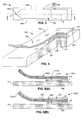
- FIGS. 1 (A) and 1 (B)are top and partial front views, respectively, of a spring material stress gauge illustrating helical twisting caused by anisotropic stress variations in a conventional spring material film;
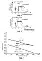
- FIG. 2is graph showing skew variations relative to biaxial stress components measured using the stress gauge shown in FIGS. 1 (A) and 1 (B);
- FIG. 3is a top view showing a spring structure according to the present invention.
- FIG. 4is a cutaway perspective view taken along line 4 — 4 of the spring structure shown in FIG. 3 ;
- FIGS. 5 (A) and 5 (B)are front section views taken along line 5 — 5 of FIG. 3 , and show alternative embodiments of spring structures formed in accordance with the present invention
- FIG. 6is a graph depicting the stress profile of a balanced spring structure
- FIG. 7is a graph depicting the stress profile of an unbalanced spring structure
- FIGS. 8 (A) through 8 (J)are simplified cross-sectional side views showing process steps associated with the fabrication of a spring structure according to several embodiments of the present invention.
- FIG. 9is a graph depicting the effects of annealing on the internal stress of a MoCr alloy
- FIG. 10is a graph depicting the effects of pressure on internal stress of a MoCr alloy measured at various points in a deposition chamber
- FIGS. 11 (A) and 11 (B)are simplified side views depicting the deposition of spring material using non-directional and directional deposition techniques, respectively;
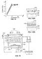
- FIG. 12is a simplified side view showing a deposition chamber utilized to produce spring structures according to another embodiment of the present invention.
- FIG. 13is a simplified top view showing a cluster tool utilized to produce spring structures in accordance with yet another embodiment of the present invention.
- FIG. 14is a flow diagram showing a process for producing spring structures using the cluster tool of FIG. 13 .
- the present inventorshave determined that the cause of helical twisting during high-volume production of spring structures is anisotropic stress in the spring material film.
- Stress anisotropyis the inequality of magnitudes of the biaxial stress along the two orthogonal principal stress axes.
- the present inventorshave also determined that stress anisotropy can occur at any point on a wafer, it can vary spatially over the wafer, and it can even be zero at certain locations, thereby producing the variety of helical twisting observed in high-volume spring structure production.
- helical twistingoccurs-when the longitudinal axis of a released spring structure is not aligned with one of the principal stress axes.
- an isotropic stressis present, the stresses along the principal stress axes differs, thereby causing the released spring finger to twist, skewing the tip from a point that is aligned with the longitudinal axis of the spring structure.
- FIGS. 1 (A) and 1 (B)are top and partial front views, respectively, of a spring material stress gauge (test structure) 10 utilized by the present inventors to illustrate helical twisting caused by anisotropic stress variations in a spring material film.
- Stress gauge 10includes several springs 11 - 1 through 11 - 8 that extend in many directions from a central region 12 . Angular positions (in degrees) are indicated around stress gauge 10 for convenience. According to the selected origin, a base portion of spring 11 - 1 is aligned generally along the 0 degree position.
- Stress gauge 10is etched from a conventional spring material film that is fabricated as described above. Accordingly, stress gauge 10 is subjected to biaxial stress whose principal components are aligned along two orthogonal directions (designated ⁇ P1 and ⁇ P2 ). The effects of stress anisotropy are quantified by measuring the skew S of a released spring, such as spring 11 - 1 of stress gauge 10 .
- the skew Sis defined as the displacement of the top-most part 11 -T of spring 11 - 1 (see FIG. 1 (B)) relative to the unreleased material at the base 11 -B of spring 11 - 1 .
- the skew Sis the result of helical bending in spring 11 - 1 , which occurs when (1) the two principal components of the biaxial stresses in the spring material film from which spring 11 - 1 is formed are unequal, and (2) the axis X of spring 10 - 1 is not aligned to either principal component.
- FIG. 2is a table that charts skews measured in the springs of stress gauge 10 (FIG. 1 ).
- FIG. 2illustrates, by making stress gauge 10 with springs pointing in many directions, the magnitude and the direction of the skew varies in relation to the principal components of biaxial stress.
- the skewis defined as positive when the helical bending is right handed.
- springscan assume either right or left handed helical bending, and at four specific orientations aligned with the principal stress components, the skew is predicted to be zero.
- the zero skew anglesare approximately 20, 110, 200 and 290 degrees relative to the selected origin.
- FIG. 3is a plan view showing a spring structure 100 according to an embodiment of the present invention.
- FIG. 4is a perspective view showing a portion of spring structure 100 , and includes a cut-away section indicated by section line 4 — 4 in FIG. 3 .
- Spring structure 100is formed on a substrate 101 , and includes a release material portion 110 and a spring finger 120 .
- Substrate 101e.g., glass
- Substrate 101e.g., glass
- Release material portion 110is formed above substrate 101 such that it contacts conductor 105 (if present).
- release material portion 110may be formed using a metal selected from the group consisting of Titanium, Copper, Aluminum, Nickel, Zirconium, and Cobalt, or formed using heavily doped silicon-, to facilitate electrical conduction between conductor 105 and spring finger 120 .
- Spring finger 120includes an anchor portion 122 and a free (i.e., cantilevered) portion 125 .
- Anchor portion 122is attached to release material portion 110 (i.e., such that release material portion 110 is located between anchor portion 122 and substrate 101 ).
- Free portion 125extends from anchor portion 122 over substrate 101 .
- spring finger 120is etched from a thin stress-engineered film that is deposited by DC magnetron sputtering or chemical vapor deposition (CVD) techniques, or deposited by plating techniques.
- the stress-engineered filmincludes or one or more materials suitable for forming a spring structure (e.g., one or more of molybdenum (Mo), a “moly-chrome” alloy (MoCr), tungsten (W), a titanium-tungsten alloy (Ti:W), chromium (Cr), nickel (Ni), silicon (Si), nitride, oxide, carbide, or diamond.
- this stress-engineered filmincludes at least one layer that has a relatively compressive (or less tensile) internal stress, and at least one layer that has a relatively tensile (or less compressive) internal stress, these different stress layers providing the upward bending bias when the underlying release material is removed, resulting in a curved, cantilever spring structure.
- layeris used herein to describe a cross-sectional region of the stress-engineered film that is formed during a given time period. For example, FIG.
- FIG. 5shows a dashed line generally delineating a first (lower) layer 126 that is formed during a first period of the sputtering process, and a second (upper) layer 127 that is formed over (or on) first layer 126 during a subsequent period of the sputtering process.
- spring structure 100is fabricated in a manner that produces at least one layer (i.e., first layer 126 and/or second layer 127 ) of spring finger 120 having isotropic internal stress before being released from substrate 101 .
- isotropic internal stressmeans that the magnitude of internal stress measured along both principal stress axes of the stress-engineered film, whether compressive or tensile, is essentially the same (i.e., within 1% or less).
- forming one or more layers of spring finger 120 with isotropic stressproduces an overall stress profile that is less anisotropic than in conventional spring structures.
- anisotropic stress distributionsare a major cause of helical twisting and spring tip skew.
- the total stress exerted on spring finger 120 upon releaseis typically less than in spring structures having anisotropic stresses (i.e., formed using conventional methods), thereby reducing or eliminating helical twisting.
- the reduction of helical twisting by incorporating one or more isotropic stress layersfacilitates high-volume production when the isotropic layer is extended over the entire wafer. Note that the relaxation of internal stress occurring in free portion 125 of spring structure 120 after release eliminates the pre-release stress isotropy. However, anchor portion 122 , which is not released, retains the one or more layers having isotropic internal stress.
- the one or more isotropic, stress layersmay include an isotropic compressive layer, an isotropic tensile layer, or both isotropic compressive and tensile layers.
- first layer 126 of spring structure 100has an isotropic compressive internal stress, and non-isotropic tensile second layer 127 is formed on first layer 126 .
- first layer 126 of spring structure 100is formed with non-isotropic compressive stress, and an isotropic tensile second layer 127 is formed thereon.
- both the compressive internal stress of first layer 126 and the tensile internal stress of second layer 127are isotropic.
- anisotropyis minimized when spring finger 120 is entirely formed from isotropic material.
- some applications that require less stringent design specificationsmay be suitably produced from spring fingers that are only partially isotropic.
- a spring structurewhen a spring structure includes both an isotropic compressive layer and an isotropic tensile layer, one or more optional structures may be utilized to prevent delamination of the spring finger.
- spring fingers 120 including bi-level stressi.e., only compressive layer 126 and tensile layer 127
- bi-level spring finger 120can have a larger moment than spring fingers that have more than two stress layers. Therefore, for a given design radius, bi-level spring finger 120 may be more likely to delaminate (i.e., separate from release material portion 110 or substrate 101 ).
- FIGS. 5 (A) and 5 (B)are cross-sectional side views showing spring structures 100 A and 100 B according to alternative embodiments of the present invention, and are taken along section line 5 — 5 of FIG. 3 .
- elements of alternative spring structures 100 A and 100 B that are similar to those of spring structure 100are identified with the same reference numbers.
- spring structure 100 Aincludes a spring finger 120 A that is formed with an intermediate layer 128 sandwiched between a lower isotropic compressive layer 126 A and an upper isotropic tensile layer 127 A.
- Intermediate layer 128is formed with an internal stress that is between the isotropic compressive internal stress of layer 126 and the tensile internal stress of layer 127 to reduce the stress gradient between compressive layer 126 A and tensile layer 127 A.
- intermediate layer 128may include two or more internal stress magnitudes, or may be represent a region whose internal stress gradually changes from compressive to tensile. Note that the intermediate stress of layer 128 may not be isotropic, but, when designed properly for a given application, isotropic layers 126 and 128 can be fabricated to substantially overcome any twisting forces exerted by anisotropy of intermediate layer 128 .
- spring structure 100 Bincludes a spring finger 120 that is similar to that described above (i.e., isotropic tensile stress layer 127 formed directly on isotropic compressive layer 126 ).
- spring structure 100 Bincludes a coating 130 (e.g., a plated metal such as Gold or Nickel) that is formed on anchor portion 122 of spring finger 120 either before or after free portion 125 is released (i.e., after release material located under-free portion 125 is removed).
- a coating 130e.g., a plated metal such as Gold or Nickel
- coating layer 130When coating layer 130 is a plated metal formed after free portion 125 is released, coating 130 may be deposited on the exposed surface of both upper layer 127 and lower layer 126 of free portion 125 , thereby providing structural and electrical characteristics that are superior to spring structures that are formed without plated metal, or having plated metal formed only on one side.
- a plated metal coating 130(FIG. 5 (B)) provides several other potentially important benefits to spring structure 100 B.
- plated metalmay be used to electroform the closure of mechanically contacted elements (e.g., an out-of-plane inductor formed using a series of spring fingers bent such that the free end of each spring finger contacts the anchor portion of an adjacent spring finger).
- Plated metalmay also be used to passivate spring finger 120 , which is important because most springy metals, such as stress-engineered metal film 220 , form surface oxides. Plated metal may also be added to increase wear resistance and lubricity. Plated metal can also provide a compression stop to limit spring compression. Moreover, plated metal may be added to strengthen spring structure 100 by adding ductility. Finally, plated metal may be added to blunt the radii of process features and defects that can arise on spring finger 120 . Note that adding plated metal (coating) 130 over free portion 125 will increase the spring constant of spring finger 120 by stiffening free portion 125 . The above-mentioned benefits are not intended to be exhaustive.
- optional conductor 105is included to provide electrical coupling of spring structure 100 to an external electrical system (not shown). Note also that the electrical coupling between spring finger 120 and conductor 105 necessitates using an electrically conductive release material to form release material portion 110 . However, electrical coupling can also be provided directly to spring finger 120 by other structures (e.g., wire bonding), thereby allowing the use of non-conducting release materials.
- a spring structureincludes at least one layer having an internal stress that is either at the compressive saturation point or the tensile saturation point of the spring material from which the spring structure is made.
- saturation pointin this context means a maximum value that the internal stress of the spring material (i.e., the spring material film) cannot exceed. Stress saturation causes the spring material to become essentially isotropic (uniform) because further applied stress pushes the spring material beyond its yield point, producing relaxation of the material that relieves the additional stress and causes the internal stress to remain at the saturated level.
- the materialis stressed (i.e., pushed) beyond its yield point, then the material is going to flow or otherwise rearrange its internal structure to relieve the excess stress, returning the material to the so-called yield point of the material.
- the stressno matter how the stress is put in, if a compressive stress greater than the compressive saturation point is put into the spring material, then the spring material is going to relax back to the level of stress that is within the strength limit of the material that is grown (i.e., to the compressive saturation point).
- a tensile stress greater than the tensile saturation pointis put into the spring material, then the spring material is going to relax back to the tensile saturation point. Therefore, by saturating the stress, the material is subjected to all the stress that the material can bear, and beyond the saturation point the internal structure no longer responds structurally to store the excess stress, and it undergoes plastic flow to accommodate additional strain imposed upon it.
- the present inventorshave observed that the compressive stress anisotropy in a spring material film tends to become smaller when the spring material has an internal stress that is at the compressive or tensile saturation point of the spring material.
- the present inventorsformed spring gauges (similar to those described above) on several wafers utilizing the methods described below that produced saturated internal stress in at least one layer, and then measured the stress along X- and Y-axes on each wafer. The differences in stress levels were also measured at different pallet locations (each pallet of the test equipment held more than one wafer; note that other deposition tools may hold only one wafer, but the wafers referred to were not processed on a cluster tool). What the inventors observed was that anisotropy over the entire wafer (and pallet) was substantially reduced when the spring material film included a saturated compressive stress layer.
- the resulting spring structureexhibits less stress anisotropy than that produced using conventional fabrication methods, thereby reducing the magnitude of helical twisting. That is, conventional techniques do not saturate the stress beyond the yield point of the material, so that the spring material film captures different stresses in different orthogonal directions; and, because the spring material film is below the yield point, these different stresses are captured or frozen into the molecular structure of the film, thereby creating anisotropy.
- the spring material films of the present embodimentare formed using much larger stresses that are close to the yield point of the spring material, then when stress is applied in one direction that tends to produce a larger stress in that direction than in another direction, the material “refuses” to store the additional stress and relaxes in the applied direction to the yield point of the material.
- the anisotropy reductionmakes sense from the standpoint of there being no margin left for anisotropy if the material is at its yield point. Note that the bulk yield point and the yield point of the growing film are not necessarily the same because the bulk and surface relaxation mechanisms can differ.
- anisotropyis minimized by fabricating a spring structure having a stress profile with only two levels, one formed by a compressive stress layer, and one formed by a tensile stress layer, both of which being grown at or near the stress saturation points of the spring material.
- lower layer 126is formed with internal stress at the compressive saturated stress level
- upper layer 127is deposited directly on lower layer 126 and formed with internal stress at the tensile saturated stress level.
- first layer 126 of spring structure 100is formed at the compressive saturation point, and an isotropic tensile second layer 127 is formed below the tensile saturation point.
- first layer 126 of spring structure 100is formed below the compressive saturation point, and second layer 127 is formed at the tensile saturation point.
- a spring structuremay include saturated layers 126 and 127 separated by a non-saturated layer 128 , such as that shown in FIG. 5 (A), or saturated layers 126 and 127 with a non-saturated layer 130 formed thereon.
- FIG. 6is a stress profile for a balanced spring structure formed from MoCr alloy (85/15 atomic-%) having a spring diameter of approximately 500 microns. As indicated in FIG. 6 , the saturation point for such a spring material at room temperature is around ⁇ 2 and +1 GPa.
- FIG. 7is a stress profile for an unbalanced spring structure formed from MoCr alloy (85/15 atomic-%) and having a spring diameter of approximately 500 microns.
- the compressive layerhas a thickness of approximately 0.4 microns
- the tensile layerhas a thickness of approximately 1.6 microns. Notice that the unbalanced spring represented by FIG. 7 is about 70% as thick as the balanced spring in FIG.
- the net stress in the unbalanced spring structureis substantially non-zero (e.g., 0.4 GPa or more, as in the example shown in FIG. 7 ).
- This substantial non-zero net stressmust be considered in the design of such unbalanced springs in that it produces diameters that are more sensitive to errors in stress and film thickness.
- the peeling momentis also reduced from 0.92 GPa- ⁇ m (produced by the balanced spring shown in FIG. 6 ) to about 0.6 GPa- ⁇ m.
- a spring structurecan be made using a saturated (first) compressive stress layer (i.e., internal stress of ⁇ 2 GPa) having a thickness of 0.2 microns, and an anisotropic (second) compressive stress layer having an internal stress of ⁇ 1 GPa and a thickness of 0.57 microns, which is formed on the isotropic layer.
- firstsaturated
- secondanisotropic
- the anisotropic compressive stress layeris relatively tensile with respect to the isotropic compressive stress layer.
- the resulting spring structurewould have a thickness of approximately 0.77 microns, a diameter of approximately 413 microns, a net stress after release of 1.29 GPa, and a net peeling moment of 1.02 GPa- ⁇ m.
- Stress saturation of spring material filmsis achieved through various methods. In accordance with one disclosed method, which is described with reference to FIGS. 8 (A) through 8 (J), stress saturation is achieved by manipulating the fabrication parameters (i.e., temperature, pressure, and RF bias) under which the spring material film is grown to generate the saturated tensile or compressive stress. Additional methods are also described below.
- fabrication parametersi.e., temperature, pressure, and RF bias
- release material layer 210is formed from an electrically conductive material, and a portion 210 A of release material layer 210 contacts a conductor 105 that is exposed on the upper surface of substrate 101 .
- release material layer 210is Titanium (Ti) that is sputter deposited onto substrate 101 to a thickness of approximately 0.2 microns or greater. Titanium provides desirable characteristics as a conductive release material layer due to its plasticity (i.e., its resistance to cracking) and its strong adhesion. Other release materials having the beneficial plastic characteristics of titanium may also be used.
- release material layer 210includes another metal, such as Copper (Cu), Aluminum (Al), Nickel (Ni), Zirconium (Zr), or Cobalt (Co). Release material layer 210 may also be formed using heavily doped silicon (Si). Further, two or more release material layers can be sequentially deposited to form a multi-layer structure. In yet another possible embodiment, any of the above-mentioned release materials can be sandwiched between two non-release material layers (i.e., materials that are not removed during the spring finger release process, described below). Alternatively, when it is not necessary to provide electrical conduction between the subsequently deposited spring material layer and a contact pad (such as conductor 105 ), release material layer 210 can be a non-conducting material such as Silicon Nitride (SiN).
- SiNSilicon Nitride
- FIGS. 8 (B) through 8 (D)show the formation and optional annealing of a spring material film in accordance with various embodiments of the present invention, discussed below.
- FIG. 8 (B)shows a lower (first) stress-engineered spring material layer 226 formed on release material layer 210 using processing techniques selected to produce a compressive internal stress in lower layer 226 that is at or near the compressive saturation point.
- spring material layer 226includes MoCr (85/15-atomic %) sputter deposited to a thickness of 0.1 to 2.5 microns using processing parameters suitable for producing saturated compressive stress.
- compressive layer 226may be generated using sputter deposition performed in an Argon atmosphere maintained at a pressure of 0.1 mT or greater, and an applied radio frequency (RF) bias of 0.2 Watt/cm 2 or greater, the deposition being performed at nominally room temperature (i.e., some heating of the substrate will occur from the deposition process).
- RFradio frequency
- this applied biaswill result in additional bombardment of the growing film, and in turn will drive the material toward the compressive saturation point.
- Higher bias power levelscan compensate for the effects of gas scattering, and thereby permit operation at higher pressures.
- FIG. 8 (C)shows an upper (second) spring material layer 227 formed on lower layer 226 using processing techniques selected to produce a tensile internal stress in upper layer 227 .
- the tensile internal stress in upper layer 227is at or near the tensile saturated stress point.
- MoCr (85/15) spring materialis sputter deposited to a thickness of 0.1 to 2.5 microns on lower layer 226 , depending on the design radius and on whether a balanced or unbalanced spring is being formed.
- substrate 101is maintained at room temperature, and sputter deposition is performed in an Argon atmosphere maintained at a pressure of 4 mT or greater, and an applied RF bias in the range of 0 to 0.25 Watts/cm 2 .
- annealingshown in FIG. 8 (D)
- the deposition process of FIGS. 8 (B) and 8 (C)is carried out at an elevated temperature that is selected to tune the saturation point of the spring material (e.g., MoCr 85/15-atomic % alloy).
- MoCr alloyis a very refractory spring material in that it melts above 2000° C.
- the present inventorslearned through experimentation that some of the stress in the MoCr alloy may be annealed out ex-situ (e.g., during the anneal process shown in FIG. 8 (D)) at fairly low temperatures (i.e., less than 350° C.).
- FIG. 9shows the effect of temperature variation on the internal stress of MoCr (85/15) alloy.
- measured datais indicated as diamonds (heating) and squares (cooling), and theoretical data (triangles).
- Theoretical behavior based on linear elastic responsesuggests that formation of saturated spring material film at a high temperature (e.g., 400° C.) would result in a net tensile shift of the stress upon cooling.
- the actual datasuggests that annealing the spring material film and/or forming the spring material film above approximately 100° C. causes relaxation that results in a tensile shift of the internal stress upon subsequent cooling. This may be particularly relevant for layers of the spring material film subjected to compressive stress, which can easily be bombarded in order to reach very high stress levels, but is difficult to make uniform.
- annealing above 100° C.may be employed to cause stress relaxation in a spring material film grown at room temperature.
- annealing in the range of 100 to approximately 400° C.may produce relaxation, resulting in substantially less internal stress upon cooling.
- Annealing significantly above approximately 350 to 400° C.is not believed to further alter the stress appreciably.
- compressive layer 226(FIG. 8 (B)) is deposited at elevated temperature (e.g., greater than 200° C., preferably 350° C.), and then tensile layer 227 (FIG. 8 (C)) is deposited at a lower deposition temperature (e.g., less than 200° C., preferably 50° C.).
- the tensile stress of layer 227is optionally kept uniform by non-saturating methods, if needed, such as using high-pressure gas scattering (discussed below).
- ⁇Y ′( ⁇ MoCr ⁇ Si )( T 2 ⁇ T 1 )
- ⁇ MoC and ⁇ Siare the expansivities of the MoCr film and silicon substrate, respectively
- T 1 and T 2are the two temperatures.
- Y′is the biaxial elastic modulus of MoCr.
- elongated spring material (first) masks 230are then patterned over a selected portion of the exposed upper layer 227 .
- exposed portions of stress-engineered material film 220 surrounding the spring material mask 230are etched using one or more etchants 240 to form a spring material island 220 - 1 . Note that this etching process is performed such that limited etching is performed in portions 210 B of release layer 210 that surround spring material island 220 - 1 such that at least a partial thickness of release layer portion 210 B remains on substrate 101 after this etching step.
- the etching stepmay be performed using, for example, a wet etching process to remove exposed portions of stress-engineered material film 220 .
- This embodimentwas successfully performed using cerric ammonium nitrate solution to remove a MoCr spring metal layer.
- Many additional etching process variations and material selectionsmay be used in place of the examples given, which are not intended to be limiting.
- FIG. 8 (G)shows spring material island 220 - 1 and release material 210 after spring material mask 230 (FIG. 8 (F)) is removed. Note again that electrical connection between conductor 105 and spring material island 220 - 1 is provided through portion 210 A of release material layer 210 .
- release (second) mask 250(e.g., photoresist) is then formed on a first portion 220 - 1 A of spring material island 220 - 1 .
- Release mask 250defines a release window RW, which exposes a second portion 220 - 1 B of spring material island 220 - 1 and surrounding portions 210 B of release material layer 210 .
- a release etchant 260e.g., a buffered oxide etch
- a release etchant 260is then use to selectively remove a portion of the release material layer from beneath the exposed portion of the spring material island to form spring finger 120 (discussed above with reference to FIGS. 1 - 3 ).
- removal of the exposed release materialcauses free portion 125 to bend away from substrate 101 due to the internal stress variations established during the formation of the spring material film (discussed above).
- anchor portion 122remains secured to substrate 101 by release material portion 110 , which is protected by release mask 250 .
- release material portion 110is formed from a conductive release material, the resulting spring structure is electrically coupled to conductor 10 . 5 .
- FIG. 8 (J)shows spring structure 100 during the removal of release mask 250
- the negative-sloped sidewall of release mask 250produces an exposed edge 250 -E under an optional post-release coating (e.g., coating 130 in FIG. 5 (A)).
- This exposed edgeallows access of a solvent that dissolves release mask using known techniques. For example, when the release mask is image-reversed photoresist, acetone can be used as the solvent. As the release mask is dissolved, residual coating portions formed thereon are lifted off. If necessary, agitation may be used to accelerate the lift-off process.
- the saturation point of the spring materialmay also tuned by adjusting the spring material composition to beneficially modify its yield point.
- Some metalsare softer and have lower yield points than Mo and Cr, and therefore the stress of a composition including these softer metals is typically saturated at lower stress values.
- materials with a ratio of elastic modulus to yield point that produces spring radii in the range desiredare selected.
- NiZr alloyshave saturated stress at lower stress values than those of MoCr alloys.
- Ni alloysNiCu alloys (e.g., Monel®), BeCu, Phosphor Bronze, or alloys of refractory materials such as Mo, Cr, Ta, W, Nb.
- the yield point of a MoCr alloymay be tuned (reduced) by including one or more “soft” metals (e.g., In, Ag, Au, Cu).
- spring material films utilizing compressive and tensile saturated stress layersproduce significant stress moments, which can result in delamination of the spring structure along spring release layer or release layer/substrate interface. It is therefore desirable to deposit spring material with isotropic stress at levels continuously (gradually) ranging within the most compressive to the most tensile values sustainable in the spring material. Continuous variation of the stress is desirable because it reduces the amount of residual stored elastic energy in the spring after release.
- the residual stress (dashed line) of a saturated stress springis shown to be substantial, whereas had the initial stress consisted of a linear rather than a stepwise profile, the residual stress (in the bending direction) would be approximately zero.
- Stepwise profiles with more than two levelsapproximate a linear profile better, and have less residual stress. Such profiles also have less abrupt stress transitions. Each transition produces internal shear within the spring.
- the present inventorshave observed that under some conditions, spring breakage is correlated with the abruptness of the stress level transitions.
- One solution to the abrupt stress level transitions associated with saturated stress springs, similar to that shown in FIG. 5 (B),is to include an additional metal layer (e.g. gold) that is usually sputtered, not plated, on the top and/or bottom of the spring material to suppress breakage.
- an additional metal layere.g. gold
- anisotropyis reduced in spring material films through variation in pressure during the deposition process.
- the arriving speciesare scattered by the sputtering gas (typically Ar gas).
- the sputtering gastypically Ar gas.
- FIG. 10shows stress vs. pressure calibration data for the Wilder tool with a 1-inch substrate to target spacing. This figure shows that there is a convergence of the stresses measured at three separate pallet positions at the highest pressure (20 mT).
- An applied RF bias(e.g., 0.05 Watts/cm 2 or more) tends to increase the bombardment of the substrate, thereby increasing the density.
- An elevated substrate temperature(e.g., 150° C. or more) will increase the surface diffusion of material incorporated into the growing film, also tending to increase the density. Heating and/or biasing the substrate will help avoid mechanical weakness.
- Properly balancing pressure, temperature and biasis believed to produce tensile stress homogeneity through gas scattering while avoiding the mechanical degradation of the film due to porosity. Homogenizing the stress via gas scattering has two distinct advantages over material saturation in that the effect can potentially operate at any stress setpoint required for the spring design, and the stress can potentially be varied continuously.
- a spring structure including both compressive (lower) and tensile (upper) layers and having a continuously varying internal stress profile therebetweenis produced by depositing at a high pressure while gradually decreasing the applied RF bias during the deposition run in order to make the stress trend from compressive to tensile.
- an isotropic spring material filmis formed using directed deposition techniques. That is, the present inventors have determined that another way to make the internal stress of the spring material film uniform in is to utilize a directional deposition process in which every atom or ion that hits the growing film is moving, at least on average, normal to the substrate.
- FIG. 11 (A)is a simplified side view showing a typical sputter deposition process used to form a spring material film 1120 on a wafer (substrate) 1101 , upon which is formed a release material layer 1110 .
- a voltageis applied to a target 1130 , which is made of spring material (e.g., MoCr), such that particulate material 1135 is separated (sputtered) from target 1130 and travels toward wafer 1101 .
- the typical sputter deposition processcauses deposition material 1135 to assume a broad angular distribution that forms spring material film 1120 .
- one or more directional deposition methodsare utilized to influence the path taken by material 1135 leaving target 1130 such that a majority of the atoms or ions that hit the growing film 1120 are moving normal to substrate 1101 .
- the present inventorshave experimentally determined that the use of directional deposition greatly reduces stress anisotropy in spring material film 1120 because material 1135 strikes all points on wafer 1101 in only one direction, thereby eliminating the differing angular distributions associated with conventional deposition methods.
- release material layer 1110is formed in the manner described above with reference to FIG. 8 (A), and further processing of the isotropic spring material film 1120 is performed as described above with reference to FIGS. 8 (E) through 8 (J).
- various directional deposition methodsthat have been previously used to produce, for example, via structures in conventional integrated circuit devices are utilized to produce isotropic spring material films.
- Such methodsinclude the use of biased ionized deposition, long throw sputtering, and collimated sputtering, each of which is described in more detail below.
- These directional deposition methodshave been used to fill high aspect ratio vias, which is important for IC (integrated circuit) manufacturing in order to reduce capacitance, lower resistance and pack more circuits onto a chip.
- ICintegrated circuit
- directed depositionis utilized to minimize internal stress anisotropy during the formation of spring material film.
- Directed depositionhas two distinct advantages over material saturation in that the effect can potentially operate at any stress setpoint required for the spring design, and the stress can potentially be varied continuously to produce the compressive-to-tensile stress profile associated with the spring material films of the present invention.
- the directionality of atoms/ionsis influenced using an applied RF bias.
- Sputter depositionis usually performed by generating a plasma in a deposition chamber containing an Argon gas atmosphere.
- the Argon gas and the sputtered spring material (e.g., metals) in a conventional plasmaconsist primarily of neutrals and positive ions. Most of the metals in a typical plasma are neutrals, and hence they will not be influenced by the applied bias.
- Much of the Argon bombardment that produces compressive stressis from reflected Argon neutrals. Utilizing an RF bias of 0.25 Watts/cm 2 or more to orient the direction of the bombardment and the depositing flux therefore is required for producing more ions.
- FIG. 12is a schematic side view showing a system for generating a highly ionized plasma in a deposition (vacuum) chamber 1200 to produce a spring material film in accordance with an embodiment of the present invention.
- a substrate (wafer) 1201is placed on a pedestal electrode 1205 at a bottom of deposition chamber 1200 .
- substrate 1201already has formed thereon a release material layer 1210 , which is formed in the manner described above.
- Located at an upper end of chamber 1200is a target 1230 , and a vertically oriented coil 1240 is wrapped around the space located between target 1230 and substrate 1201 .
- a DC power supply 1250negatively biases target 1230 .
- An RF power source 1253supplies electrical power in the megahertz range to inductive coil 1240 .
- the DC voltage applied between target 1230 and substrate 1201causes the processing gas supplied to the chamber to discharge and form a plasma.
- the RF coil power inductively coupled into chamber 1200 by coil 1240increases the density of the plasma.
- Magnets 1260 disposed above target 1240significantly increase the density of the plasma adjacent to target 1230 in order to increase the sputtering efficiency.
- Another RF power source 1257applies electrical power in the frequency range of 100 kHz to a few megahertz to pedestal 1205 in order to bias it with respect to the plasma. This technique is described in S. M. Rossnagel and J. Hopwood, “Metal Ion Deposition from Ionized Magnetron Sputtering Discharge”, J.
- Pulsed sputteringis another method for producing more ions to form isotropic spring material films in accordance with the present invention.
- High current pulsed sputteringis a way to make lots of ions.
- Ulf Helmersson in Linköping SwedenThese developments use pulses of hundreds of amps, and megawatts of power, that last for 10's or 100's of microseconds (see Gudmundsson, J. T.; Alami, J.; Helmersson, U., “Evolution of the Electron Energy Distribution and Plasma Parameters in a Pulsed Magnetron Discharge”, Applied Physics Letters, 78(22), pp 3427-9 (2001); see also Helmersson, U.; Khan, Z.
- spring materialsare grown using “long throw” techniques in which a wafer (substrate) is placed one diameter of the wafer or more away from the target (i.e., when the wafer is stationary). The farther away the sputter source, the more collimated the deposited material becomes.
- This approach to making sputter systemshas also been used for filling vias.
- the distance between the target and the substrate in a cluster toolin about 2 inches (less than one wafer diameter). If however the distance is increased to one wafer diameter or more, the range of angles with which the flux arrives is reduced. By cutting out shallowest angles of the deposition, the stress anisotropy is believed to be reduced.
- the distancemust be on the order of the size of the holder containing the substrates, and its range of motion, if any, relative to the target.
- the present inventorshave looked into various deposition geometries and wafer handling configurations.
- cross contaminationhas produced some unexpected results. These include metal contamination altering the stress level in the film for a given process condition, electrochemical effects during etching resulting from interface intermixing, and the presence of residues after etching due to insoluble contaminants. All of the effects occur because single chamber systems have sputter cathodes for materials that form the release, spring and cladding layers of the spring. When one cathode is sputtering and the other is exposed, the exposed cathode accumulates contamination build-up on its target.
- spring structuresare produced using an integrated multi-chamber tool (“cluster tool”) that is configured such that separate chambers are utilized for each of the sputter targets and the etching function, thereby maintaining the integrity of the sputter targets throughout the production process.
- cluster toolintegrated multi-chamber tool
- FIG. 13is a simplified top plan view showing a cluster tool 1300 configured in accordance with an embodiment of the present invention.
- One such cluster toolis the Endura RTM 5500 platform, which is functionally described by Tepman et al. in U.S. Pat. No. 5,186,718.
- Wafers 1301are loaded into the system by two independently operated loadlock chambers 1305 configured to transfer wafers into and out of the system from wafer cassettes loaded into the respective loadlock chambers.
- the pressure of a first wafer transfer chamber 1304 to which the loadlocks can be selectively connected via unillustrated slit valvescan be regulated.
- a first robot 1306 located in the first transfer chamber 1304transfers the wafer from the cassette to one of two wafer orienters 1308 and then to a degassing orienting chamber 1312 .
- First robot 1306then passes the wafer into an intermediately placed plasma preclean chamber 1314 , from which a second robot 1316 transfers it to a second transfer chamber 1318 , which is kept at a low pressure.
- Second robot 1316selectively transfers wafers to and from reaction chambers arranged around its periphery.
- reaction chambersarranged around its periphery.
- first deposition chamber 1320is utilized to form a release material layer on each substrate according to the methods described above, one or more second deposition chambers 1322 and 1324 are used to form spring material film on the release material layer.
- first deposition chamberis configured with a suitable target formed from a selected release material (e.g., Titanium), and second deposition chambers 1322 and/or 1324 are configured with suitable targets formed from a selected spring material (e.g., MoCr alloy). Accordingly, as indicated in the flow diagram shown in FIG.
- each wafer 1301is moved into first chamber 1320 (block 1410 ) for release layer formation (block 1420 ), and then moved to second chamber 1322 / 1324 (block 1430 ) for spring material film formation (block 1440 ) according to one or more of the methods described above.
- both chambers 1322 and 1324are configured with similar spring material targets and otherwise optimized for the respective different processes. For example, if the compressive layer and tensile layer are formed at different temperatures, then chambers 1322 and 1324 are maintained at these different temperatures to minimize the time required to change between these two temperatures.
- substrates 1301are removed from the cluster tool, and transferred to a suitable third chamber (block 1450 in FIG. 14 ) for subsequent etching and spring finger formation (block 1460 ) according to the process described above.
- a suitable third chamberblock 1450 in FIG. 14
- etching and spring finger formationblock 1460
- a multi-chamber sputter tool with chambers arranged in a vertical inline geometry and configured as described abovecan be used in place of cluster tool 1300 .
Landscapes
- Chemical & Material Sciences (AREA)
- Engineering & Computer Science (AREA)
- Physics & Mathematics (AREA)
- Microelectronics & Electronic Packaging (AREA)
- Manufacturing & Machinery (AREA)
- Metallurgy (AREA)
- Organic Chemistry (AREA)
- Materials Engineering (AREA)
- Chemical Kinetics & Catalysis (AREA)
- General Physics & Mathematics (AREA)
- Mechanical Engineering (AREA)
- Computer Hardware Design (AREA)
- Condensed Matter Physics & Semiconductors (AREA)
- Power Engineering (AREA)
- Geometry (AREA)
- Micromachines (AREA)
- Springs (AREA)
Abstract
Description
Δσ=Y′(αMoCr−αSi)(T2−T1)
where αMoCand αSiare the expansivities of the MoCr film and silicon substrate, respectively, and T1 and T2are the two temperatures. Y′ is the biaxial elastic modulus of MoCr.
Claims (58)
Priority Applications (5)
| Application Number | Priority Date | Filing Date | Title |
|---|---|---|---|
| US10/121,644US6866255B2 (en) | 2002-04-12 | 2002-04-12 | Sputtered spring films with low stress anisotropy |
| EP03252001.7AEP1353443B1 (en) | 2002-04-12 | 2003-03-28 | Spring contact |
| JP2003104737AJP4454246B2 (en) | 2002-04-12 | 2003-04-09 | Spring structure, method for manufacturing spring structure, integrated processing tool, and method for manufacturing spring structure on wafer |
| US11/029,618US7172707B2 (en) | 2002-04-12 | 2005-01-05 | Sputtered spring films with low stress anisotropy |
| US11/611,823US20070117234A1 (en) | 2002-04-12 | 2006-12-15 | Sputtered Spring Films With Low Stress Anisotropy |
Applications Claiming Priority (1)
| Application Number | Priority Date | Filing Date | Title |
|---|---|---|---|
| US10/121,644US6866255B2 (en) | 2002-04-12 | 2002-04-12 | Sputtered spring films with low stress anisotropy |
Related Child Applications (1)
| Application Number | Title | Priority Date | Filing Date |
|---|---|---|---|
| US11/029,618DivisionUS7172707B2 (en) | 2002-04-12 | 2005-01-05 | Sputtered spring films with low stress anisotropy |
Publications (2)
| Publication Number | Publication Date |
|---|---|
| US20030192476A1 US20030192476A1 (en) | 2003-10-16 |
| US6866255B2true US6866255B2 (en) | 2005-03-15 |
Family
ID=28454029
Family Applications (3)
| Application Number | Title | Priority Date | Filing Date |
|---|---|---|---|
| US10/121,644Expired - LifetimeUS6866255B2 (en) | 2002-04-12 | 2002-04-12 | Sputtered spring films with low stress anisotropy |
| US11/029,618Expired - Fee RelatedUS7172707B2 (en) | 2002-04-12 | 2005-01-05 | Sputtered spring films with low stress anisotropy |
| US11/611,823AbandonedUS20070117234A1 (en) | 2002-04-12 | 2006-12-15 | Sputtered Spring Films With Low Stress Anisotropy |
Family Applications After (2)
| Application Number | Title | Priority Date | Filing Date |
|---|---|---|---|
| US11/029,618Expired - Fee RelatedUS7172707B2 (en) | 2002-04-12 | 2005-01-05 | Sputtered spring films with low stress anisotropy |
| US11/611,823AbandonedUS20070117234A1 (en) | 2002-04-12 | 2006-12-15 | Sputtered Spring Films With Low Stress Anisotropy |
Country Status (3)
| Country | Link |
|---|---|
| US (3) | US6866255B2 (en) |
| EP (1) | EP1353443B1 (en) |
| JP (1) | JP4454246B2 (en) |
Cited By (14)
| Publication number | Priority date | Publication date | Assignee | Title |
|---|---|---|---|---|
| US20050011748A1 (en)* | 2001-08-25 | 2005-01-20 | Thomas Beck | Method for producing a nanostructured funcitonal coating and a coating that can be produced according to said method |
| US20050249451A1 (en)* | 2004-04-27 | 2005-11-10 | Tom Baehr-Jones | Integrated plasmon and dielectric waveguides |
| US20050263686A1 (en)* | 2004-04-27 | 2005-12-01 | Tom Baehr-Jones | Near field scanning microscope probe and method for fabricating same |
| US20050286110A1 (en)* | 2004-06-25 | 2005-12-29 | Industrial Technology Research Institute | MEMS optical switch with self-assembly structure |
| US20060001159A1 (en)* | 2004-06-30 | 2006-01-05 | Garcia Jason A | Electronic assembly having multi-material interconnects |
| US20060180927A1 (en)* | 2005-02-14 | 2006-08-17 | Daisuke Takai | Contact structure and method for manufacturing the same |
| US20060281297A1 (en)* | 2004-01-27 | 2006-12-14 | Nobuaki Ogawa | Multilayer electronic part and structure for mounting multilayer electronic part |
| US20080014728A1 (en)* | 2006-06-29 | 2008-01-17 | Agere Systems Inc. | Method to improve metal defects in semiconductor device fabrication |
| US20100285700A1 (en)* | 2004-10-21 | 2010-11-11 | Palo Alto Research Center Incorporated | Curved Spring Structure With Downturned Tip |
| CN102305256A (en)* | 2011-09-06 | 2012-01-04 | 复旦大学 | Metal micrometer/nanometer spring as well as preparation method and application thereof |
| US20120308053A1 (en)* | 2011-06-01 | 2012-12-06 | Infineon Technologies Ag | Plate, Transducer and Methods for Making and Operating a Transducer |
| US20150348268A1 (en)* | 2002-01-04 | 2015-12-03 | Aol Inc. | Registration of separations |
| US20160362780A1 (en)* | 2015-01-11 | 2016-12-15 | Soleras Advanced Coatings Bvba | A Cover with a Sensor System for a Configurable Measuring System for a Configurable Sputtering System |
| US20190259697A1 (en)* | 2017-11-28 | 2019-08-22 | Samsung Electro-Mechanics Co., Ltd. | Carrier substrate and method of manufacturing semiconductor package using the same |
Families Citing this family (35)
| Publication number | Priority date | Publication date | Assignee | Title |
|---|---|---|---|---|
| US6866255B2 (en)* | 2002-04-12 | 2005-03-15 | Xerox Corporation | Sputtered spring films with low stress anisotropy |
| US7082684B2 (en)* | 2004-08-04 | 2006-08-01 | Palo Alto Research Center Incorporated | Intermetallic spring structure |
| KR100670946B1 (en)* | 2005-10-27 | 2007-01-17 | 학교법인 포항공과대학교 | Multiscale cantilever structure having nano-sized microholes and method for manufacturing the same |
| US7825567B2 (en)* | 2006-01-20 | 2010-11-02 | Panasonic Corporation | Three-dimensional structure and its manufacturing method |
| US7713388B2 (en)* | 2006-02-27 | 2010-05-11 | Palo Alto Research Center Incorporated | Out-of-plane spring structures on a substrate |
| US7470974B2 (en)* | 2006-07-14 | 2008-12-30 | Cabot Corporation | Substantially transparent material for use with light-emitting device |
| US7465681B2 (en)* | 2006-08-25 | 2008-12-16 | Corning Incorporated | Method for producing smooth, dense optical films |
| US7545014B2 (en) | 2006-10-12 | 2009-06-09 | Hewlett-Packard Development Company, L.P. | Three-dimensional resonant cells with tilt up fabrication |
| US20090140433A1 (en)* | 2007-11-30 | 2009-06-04 | Alces Technology, Inc. | MEMS chip-to-chip interconnects |
| US8568941B2 (en) | 2009-03-04 | 2013-10-29 | Panasonic Corporation | Fuel cell separator and fuel cell including same |
| TWI404428B (en)* | 2009-11-25 | 2013-08-01 | Ind Tech Res Inst | Acoustics transducer |
| US8404369B2 (en)* | 2010-08-03 | 2013-03-26 | WD Media, LLC | Electroless coated disks for high temperature applications and methods of making the same |
| KR102013503B1 (en)* | 2011-09-28 | 2019-08-22 | 뷔흘러 알제나우 게엠베하 | Method and apparatus for producing a reflection-reducing layer on an substrate |
| US9007818B2 (en) | 2012-03-22 | 2015-04-14 | Micron Technology, Inc. | Memory cells, semiconductor device structures, systems including such cells, and methods of fabrication |
| US8923038B2 (en) | 2012-06-19 | 2014-12-30 | Micron Technology, Inc. | Memory cells, semiconductor device structures, memory systems, and methods of fabrication |
| US9054030B2 (en) | 2012-06-19 | 2015-06-09 | Micron Technology, Inc. | Memory cells, semiconductor device structures, memory systems, and methods of fabrication |
| US9388494B2 (en) | 2012-06-25 | 2016-07-12 | Novellus Systems, Inc. | Suppression of parasitic deposition in a substrate processing system by suppressing precursor flow and plasma outside of substrate region |
| US9379315B2 (en) | 2013-03-12 | 2016-06-28 | Micron Technology, Inc. | Memory cells, methods of fabrication, semiconductor device structures, and memory systems |
| US9368714B2 (en) | 2013-07-01 | 2016-06-14 | Micron Technology, Inc. | Memory cells, methods of operation and fabrication, semiconductor device structures, and memory systems |
| US9466787B2 (en) | 2013-07-23 | 2016-10-11 | Micron Technology, Inc. | Memory cells, methods of fabrication, semiconductor device structures, memory systems, and electronic systems |
| US9461242B2 (en) | 2013-09-13 | 2016-10-04 | Micron Technology, Inc. | Magnetic memory cells, methods of fabrication, semiconductor devices, memory systems, and electronic systems |
| US9608197B2 (en) | 2013-09-18 | 2017-03-28 | Micron Technology, Inc. | Memory cells, methods of fabrication, and semiconductor devices |
| US10454024B2 (en) | 2014-02-28 | 2019-10-22 | Micron Technology, Inc. | Memory cells, methods of fabrication, and memory devices |
| US9281466B2 (en) | 2014-04-09 | 2016-03-08 | Micron Technology, Inc. | Memory cells, semiconductor structures, semiconductor devices, and methods of fabrication |
| US9269888B2 (en) | 2014-04-18 | 2016-02-23 | Micron Technology, Inc. | Memory cells, methods of fabrication, and semiconductor devices |
| US9617638B2 (en) | 2014-07-30 | 2017-04-11 | Lam Research Corporation | Methods and apparatuses for showerhead backside parasitic plasma suppression in a secondary purge enabled ALD system |
| US9349945B2 (en) | 2014-10-16 | 2016-05-24 | Micron Technology, Inc. | Memory cells, semiconductor devices, and methods of fabrication |
| US9768377B2 (en) | 2014-12-02 | 2017-09-19 | Micron Technology, Inc. | Magnetic cell structures, and methods of fabrication |
| CN104555908A (en)* | 2014-12-04 | 2015-04-29 | 复旦大学 | Machining method of micro-spring |
| US10439131B2 (en) | 2015-01-15 | 2019-10-08 | Micron Technology, Inc. | Methods of forming semiconductor devices including tunnel barrier materials |
| US9508547B1 (en)* | 2015-08-17 | 2016-11-29 | Lam Research Corporation | Composition-matched curtain gas mixtures for edge uniformity modulation in large-volume ALD reactors |
| US9738977B1 (en) | 2016-06-17 | 2017-08-22 | Lam Research Corporation | Showerhead curtain gas method and system for film profile modulation |
| US10563304B2 (en)* | 2017-04-07 | 2020-02-18 | Applied Materials, Inc. | Methods and apparatus for dynamically treating atomic layer deposition films in physical vapor deposition chambers |
| US12087573B2 (en) | 2019-07-17 | 2024-09-10 | Lam Research Corporation | Modulation of oxidation profile for substrate processing |
| US11201275B1 (en)* | 2020-06-10 | 2021-12-14 | Palo Alto Research Center Incorporated | Superconducting stress-engineered micro-fabricated springs |
Citations (49)
| Publication number | Priority date | Publication date | Assignee | Title |
|---|---|---|---|---|
| US3842189A (en) | 1973-01-08 | 1974-10-15 | Rca Corp | Contact array and method of making the same |
| US3952404A (en) | 1973-07-30 | 1976-04-27 | Sharp Kabushiki Kaisha | Beam lead formation method |
| US4189342A (en) | 1971-10-07 | 1980-02-19 | U.S. Philips Corporation | Semiconductor device comprising projecting contact layers |
| US4423401A (en) | 1982-07-21 | 1983-12-27 | Tektronix, Inc. | Thin-film electrothermal device |
| US4468014A (en)* | 1980-09-15 | 1984-08-28 | Paccar, Inc. | Composite leaf spring |
| US4821148A (en) | 1985-06-14 | 1989-04-11 | Hitachi, Ltd. | Resin packaged semiconductor device having a protective layer made of a metal-organic matter compound |
| US5280139A (en) | 1990-03-01 | 1994-01-18 | Motorola, Inc. | Selectively releasing conductive runner and substrate assembly |
| US5399232A (en) | 1989-01-17 | 1995-03-21 | The Board Of Trustees Of The Leland Stanford Junior University | Microfabricated cantilever stylus with integrated pyramidal tip |
| US5414298A (en) | 1993-03-26 | 1995-05-09 | Tessera, Inc. | Semiconductor chip assemblies and components with pressure contact |
| US5465611A (en)* | 1993-03-30 | 1995-11-14 | Imm Institut Fur Mikrotechnik Gmbh | Sensor head for use in atomic force microscopy and method for its production |
| US5513518A (en) | 1994-05-19 | 1996-05-07 | Molecular Imaging Corporation | Magnetic modulation of force sensor for AC detection in an atomic force microscope |
| US5515719A (en) | 1994-05-19 | 1996-05-14 | Molecular Imaging Corporation | Controlled force microscope for operation in liquids |
| US5534662A (en)* | 1994-08-31 | 1996-07-09 | International Business Machines Corporation | Chassis mounted electromagnetic interference grounding assembly for electronic modules |
| US5613861A (en)* | 1995-06-07 | 1997-03-25 | Xerox Corporation | Photolithographically patterned spring contact |
| US5665648A (en) | 1995-12-21 | 1997-09-09 | Hughes Electronics | Integrated circuit spring contact fabrication methods |
| US5780885A (en) | 1992-12-28 | 1998-07-14 | Commissariat A L'energie Atomique | Accelerometers using silicon on insulator technology |
| US5831181A (en) | 1995-09-29 | 1998-11-03 | The Regents Of The University Of California | Automated tool for precision machining and imaging |
| WO1999018445A1 (en) | 1997-10-02 | 1999-04-15 | New Jersey Institute Of Technology | Micromachined element and method of fabrication thereof |
| US5939623A (en) | 1996-02-20 | 1999-08-17 | Seiko Instruments Inc. | Scanning type near field interatomic force microscope |
| US5944537A (en)* | 1997-12-15 | 1999-08-31 | Xerox Corporation | Photolithographically patterned spring contact and apparatus and methods for electrically contacting devices |
| US5959516A (en) | 1998-01-08 | 1999-09-28 | Rockwell Science Center, Llc | Tunable-trimmable micro electro mechanical system (MEMS) capacitor |
| US5960147A (en) | 1996-04-09 | 1999-09-28 | Seiko Instruments Inc. | Probe, manufacturing method therefor and scanning probe microscope |
| US5979892A (en) | 1998-05-15 | 1999-11-09 | Xerox Corporation | Controlled cilia for object manipulation |
| US6011261A (en) | 1997-03-04 | 2000-01-04 | Canon Kabushiki Kaisha | Probe formed of mono-crystalline SI, the manufacturing method thereof, and an information processing device using the probe |
| WO2000033089A2 (en) | 1998-12-02 | 2000-06-08 | Formfactor, Inc. | Lithographic contact elements |
| US6117694A (en) | 1994-07-07 | 2000-09-12 | Tessera, Inc. | Flexible lead structures and methods of making same |
| US6194774B1 (en) | 1999-03-10 | 2001-02-27 | Samsung Electronics Co., Ltd. | Inductor including bonding wires |
| US6213789B1 (en)* | 1999-12-15 | 2001-04-10 | Xerox Corporation | Method and apparatus for interconnecting devices using an adhesive |
| US6238533B1 (en) | 1995-08-07 | 2001-05-29 | Applied Materials, Inc. | Integrated PVD system for aluminum hole filling using ionized metal adhesion layer |
| US6249039B1 (en) | 1998-09-10 | 2001-06-19 | Bourns, Inc. | Integrated inductive components and method of fabricating such components |
| US6252175B1 (en) | 1993-11-16 | 2001-06-26 | Igor Y. Khandros | Electronic assembly comprising a substrate and a plurality of springable interconnection elements secured to terminals of the substrate |
| WO2001048870A2 (en) | 1999-12-28 | 2001-07-05 | Formfactor, Inc. | Interconnect for microelectronic structures with enhanced spring characteristics |
| US6290510B1 (en) | 2000-07-27 | 2001-09-18 | Xerox Corporation | Spring structure with self-aligned release material |
| US6299462B1 (en)* | 1999-11-15 | 2001-10-09 | Xerox Corporation | Self positioning, passive MEMS mirror structures |
| US6352454B1 (en)* | 1999-10-20 | 2002-03-05 | Xerox Corporation | Wear-resistant spring contacts |
| US20020040884A1 (en) | 1997-08-27 | 2002-04-11 | Thomas Hantschel | Probe tip configuration and a method of fabrication thereof |
| US20020047091A1 (en) | 2000-09-18 | 2002-04-25 | Thomas Hantschel | Probe tip and method of manufacturing tips and probes for detecting microcurrent or microforce |
| US20020055282A1 (en) | 2000-11-09 | 2002-05-09 | Eldridge Benjamin N. | Electronic components with plurality of contoured microelectronic spring contacts |
| US6392524B1 (en)* | 2000-06-09 | 2002-05-21 | Xerox Corporation | Photolithographically-patterned out-of-plane coil structures and method of making |
| US20020079445A1 (en) | 2000-09-15 | 2002-06-27 | Thomas Hantschel | Probe and method of manufacturing mounted AFM probes |
| US6441359B1 (en) | 1998-10-20 | 2002-08-27 | The Board Of Trustees Of The Leland Stanford Junior University | Near field optical scanning system employing microfabricated solid immersion lens |
| US6455885B1 (en) | 1998-12-21 | 2002-09-24 | Megic Corporation | Inductor structure for high performance system-on-chip using post passivation process |
| US6499216B1 (en) | 1994-07-07 | 2002-12-31 | Tessera, Inc. | Methods and structures for electronic probing arrays |
| US6505398B2 (en)* | 2000-12-04 | 2003-01-14 | Kavlico Corporation | Very high pressure miniature sensing and mounting technique |
| US20030010615A1 (en) | 2001-07-11 | 2003-01-16 | Xerox Corporation | Microspring with conductive coating deposited on tip after release |
| US6528785B1 (en) | 1998-12-03 | 2003-03-04 | Daiken Chemical Co., Ltd. | Fusion-welded nanotube surface signal probe and method of attaching nanotube to probe holder |
| US6528350B2 (en) | 2001-05-21 | 2003-03-04 | Xerox Corporation | Method for fabricating a metal plated spring structure |
| US6556648B1 (en)* | 2000-11-07 | 2003-04-29 | Asml Netherlands B.V. | Lithographic apparatus, device manufacturing method, and device manufactured thereby |
| US6578410B1 (en) | 2001-08-10 | 2003-06-17 | Jacob Israelachvili | Resistive cantilever spring for probe microscopy |
Family Cites Families (8)
| Publication number | Priority date | Publication date | Assignee | Title |
|---|---|---|---|---|
| JPH06120218A (en)* | 1992-10-02 | 1994-04-28 | Miyazaki Oki Electric Co Ltd | Metal wiring of semiconductor element |
| US5633552A (en)* | 1993-06-04 | 1997-05-27 | The Regents Of The University Of California | Cantilever pressure transducer |
| US5536963A (en)* | 1994-05-11 | 1996-07-16 | Regents Of The University Of Minnesota | Microdevice with ferroelectric for sensing or applying a force |
| US6298685B1 (en)* | 1999-11-03 | 2001-10-09 | Applied Materials, Inc. | Consecutive deposition system |
| US6436819B1 (en)* | 2000-02-01 | 2002-08-20 | Applied Materials, Inc. | Nitrogen treatment of a metal nitride/metal stack |
| US7037830B1 (en)* | 2000-02-16 | 2006-05-02 | Novellus Systems, Inc. | PVD deposition process for enhanced properties of metal films |
| US20020192948A1 (en)* | 2001-06-15 | 2002-12-19 | Applied Materials, Inc. | Integrated barrier layer structure for copper contact level metallization |
| US6866255B2 (en)* | 2002-04-12 | 2005-03-15 | Xerox Corporation | Sputtered spring films with low stress anisotropy |
- 2002
- 2002-04-12USUS10/121,644patent/US6866255B2/ennot_activeExpired - Lifetime
- 2003
- 2003-03-28EPEP03252001.7Apatent/EP1353443B1/ennot_activeExpired - Lifetime
- 2003-04-09JPJP2003104737Apatent/JP4454246B2/ennot_activeExpired - Fee Related
- 2005
- 2005-01-05USUS11/029,618patent/US7172707B2/ennot_activeExpired - Fee Related
- 2006
- 2006-12-15USUS11/611,823patent/US20070117234A1/ennot_activeAbandoned
Patent Citations (56)
| Publication number | Priority date | Publication date | Assignee | Title |
|---|---|---|---|---|
| US4189342A (en) | 1971-10-07 | 1980-02-19 | U.S. Philips Corporation | Semiconductor device comprising projecting contact layers |
| US3842189A (en) | 1973-01-08 | 1974-10-15 | Rca Corp | Contact array and method of making the same |
| US3952404A (en) | 1973-07-30 | 1976-04-27 | Sharp Kabushiki Kaisha | Beam lead formation method |
| US4468014A (en)* | 1980-09-15 | 1984-08-28 | Paccar, Inc. | Composite leaf spring |
| US4423401A (en) | 1982-07-21 | 1983-12-27 | Tektronix, Inc. | Thin-film electrothermal device |
| US4821148A (en) | 1985-06-14 | 1989-04-11 | Hitachi, Ltd. | Resin packaged semiconductor device having a protective layer made of a metal-organic matter compound |
| US5399232A (en) | 1989-01-17 | 1995-03-21 | The Board Of Trustees Of The Leland Stanford Junior University | Microfabricated cantilever stylus with integrated pyramidal tip |
| US5280139A (en) | 1990-03-01 | 1994-01-18 | Motorola, Inc. | Selectively releasing conductive runner and substrate assembly |
| US5780885A (en) | 1992-12-28 | 1998-07-14 | Commissariat A L'energie Atomique | Accelerometers using silicon on insulator technology |
| US5414298A (en) | 1993-03-26 | 1995-05-09 | Tessera, Inc. | Semiconductor chip assemblies and components with pressure contact |
| US5465611A (en)* | 1993-03-30 | 1995-11-14 | Imm Institut Fur Mikrotechnik Gmbh | Sensor head for use in atomic force microscopy and method for its production |
| US6252175B1 (en) | 1993-11-16 | 2001-06-26 | Igor Y. Khandros | Electronic assembly comprising a substrate and a plurality of springable interconnection elements secured to terminals of the substrate |
| US5513518A (en) | 1994-05-19 | 1996-05-07 | Molecular Imaging Corporation | Magnetic modulation of force sensor for AC detection in an atomic force microscope |
| US5515719A (en) | 1994-05-19 | 1996-05-14 | Molecular Imaging Corporation | Controlled force microscope for operation in liquids |
| US5612491A (en) | 1994-05-19 | 1997-03-18 | Molecular Imaging Corporation | Formation of a magnetic film on an atomic force microscope cantilever |
| US6499216B1 (en) | 1994-07-07 | 2002-12-31 | Tessera, Inc. | Methods and structures for electronic probing arrays |
| US6117694A (en) | 1994-07-07 | 2000-09-12 | Tessera, Inc. | Flexible lead structures and methods of making same |
| US5534662A (en)* | 1994-08-31 | 1996-07-09 | International Business Machines Corporation | Chassis mounted electromagnetic interference grounding assembly for electronic modules |
| US6184699B1 (en) | 1995-06-07 | 2001-02-06 | Xerox Corporation | Photolithographically patterned spring contact |
| US6264477B1 (en) | 1995-06-07 | 2001-07-24 | Xerox Corporation | Photolithographically patterned spring contact |
| US5914218A (en) | 1995-06-07 | 1999-06-22 | Xerox Corporation | Method for forming a spring contact |
| US5613861A (en)* | 1995-06-07 | 1997-03-25 | Xerox Corporation | Photolithographically patterned spring contact |
| US6184065B1 (en) | 1995-06-07 | 2001-02-06 | Xerox Corporation | Photolithographically patterned spring contact |
| US5848685A (en) | 1995-06-07 | 1998-12-15 | Xerox Corporation | Photolithographically patterned spring contact |
| US6238533B1 (en) | 1995-08-07 | 2001-05-29 | Applied Materials, Inc. | Integrated PVD system for aluminum hole filling using ionized metal adhesion layer |
| US5831181A (en) | 1995-09-29 | 1998-11-03 | The Regents Of The University Of California | Automated tool for precision machining and imaging |
| US5665648A (en) | 1995-12-21 | 1997-09-09 | Hughes Electronics | Integrated circuit spring contact fabrication methods |
| US5939623A (en) | 1996-02-20 | 1999-08-17 | Seiko Instruments Inc. | Scanning type near field interatomic force microscope |
| US5960147A (en) | 1996-04-09 | 1999-09-28 | Seiko Instruments Inc. | Probe, manufacturing method therefor and scanning probe microscope |
| US6011261A (en) | 1997-03-04 | 2000-01-04 | Canon Kabushiki Kaisha | Probe formed of mono-crystalline SI, the manufacturing method thereof, and an information processing device using the probe |
| US20020040884A1 (en) | 1997-08-27 | 2002-04-11 | Thomas Hantschel | Probe tip configuration and a method of fabrication thereof |
| WO1999018445A1 (en) | 1997-10-02 | 1999-04-15 | New Jersey Institute Of Technology | Micromachined element and method of fabrication thereof |
| US5944537A (en)* | 1997-12-15 | 1999-08-31 | Xerox Corporation | Photolithographically patterned spring contact and apparatus and methods for electrically contacting devices |
| US5959516A (en) | 1998-01-08 | 1999-09-28 | Rockwell Science Center, Llc | Tunable-trimmable micro electro mechanical system (MEMS) capacitor |
| US5979892A (en) | 1998-05-15 | 1999-11-09 | Xerox Corporation | Controlled cilia for object manipulation |
| US6249039B1 (en) | 1998-09-10 | 2001-06-19 | Bourns, Inc. | Integrated inductive components and method of fabricating such components |
| US6441359B1 (en) | 1998-10-20 | 2002-08-27 | The Board Of Trustees Of The Leland Stanford Junior University | Near field optical scanning system employing microfabricated solid immersion lens |
| WO2000033089A2 (en) | 1998-12-02 | 2000-06-08 | Formfactor, Inc. | Lithographic contact elements |
| US6528785B1 (en) | 1998-12-03 | 2003-03-04 | Daiken Chemical Co., Ltd. | Fusion-welded nanotube surface signal probe and method of attaching nanotube to probe holder |
| US6455885B1 (en) | 1998-12-21 | 2002-09-24 | Megic Corporation | Inductor structure for high performance system-on-chip using post passivation process |
| US6194774B1 (en) | 1999-03-10 | 2001-02-27 | Samsung Electronics Co., Ltd. | Inductor including bonding wires |
| US6352454B1 (en)* | 1999-10-20 | 2002-03-05 | Xerox Corporation | Wear-resistant spring contacts |
| US6299462B1 (en)* | 1999-11-15 | 2001-10-09 | Xerox Corporation | Self positioning, passive MEMS mirror structures |
| US6213789B1 (en)* | 1999-12-15 | 2001-04-10 | Xerox Corporation | Method and apparatus for interconnecting devices using an adhesive |
| WO2001048870A2 (en) | 1999-12-28 | 2001-07-05 | Formfactor, Inc. | Interconnect for microelectronic structures with enhanced spring characteristics |
| US6392524B1 (en)* | 2000-06-09 | 2002-05-21 | Xerox Corporation | Photolithographically-patterned out-of-plane coil structures and method of making |
| US20020013070A1 (en) | 2000-07-27 | 2002-01-31 | Xerox Corporation | Spring structure with self-aligned release material |
| US6290510B1 (en) | 2000-07-27 | 2001-09-18 | Xerox Corporation | Spring structure with self-aligned release material |
| US20020079445A1 (en) | 2000-09-15 | 2002-06-27 | Thomas Hantschel | Probe and method of manufacturing mounted AFM probes |
| US20020047091A1 (en) | 2000-09-18 | 2002-04-25 | Thomas Hantschel | Probe tip and method of manufacturing tips and probes for detecting microcurrent or microforce |
| US6556648B1 (en)* | 2000-11-07 | 2003-04-29 | Asml Netherlands B.V. | Lithographic apparatus, device manufacturing method, and device manufactured thereby |
| US20020055282A1 (en) | 2000-11-09 | 2002-05-09 | Eldridge Benjamin N. | Electronic components with plurality of contoured microelectronic spring contacts |
| US6505398B2 (en)* | 2000-12-04 | 2003-01-14 | Kavlico Corporation | Very high pressure miniature sensing and mounting technique |
| US6528350B2 (en) | 2001-05-21 | 2003-03-04 | Xerox Corporation | Method for fabricating a metal plated spring structure |
| US20030010615A1 (en) | 2001-07-11 | 2003-01-16 | Xerox Corporation | Microspring with conductive coating deposited on tip after release |
| US6578410B1 (en) | 2001-08-10 | 2003-06-17 | Jacob Israelachvili | Resistive cantilever spring for probe microscopy |
Non-Patent Citations (15)
| Title |
|---|
| "Pinnacle Plus+ Pulsed DC Power Supply: New Horizons in Reactive Sputtering Performance," Advanced Energy Industries, Inc., 4 pgs. |
| Chang et al., "Large Suspended Inductors on Silicon and Their Use in a 2-mum CMOS RF Amplifier," IEEE Electron Device Letters, vol. 14, No. 5, May 1993, pp. 246-248. |
| Chen et al., "Nanostructure patterns written in polycarbonate by a bent optical fiber probe," J. Vac. Sci. Technol. B 19(6), Nov./Dec. 2001, pp. 2299-2300. |
| Craninckx et al., "A CMOS 1.8GHz Low-Phase-Noise-Voltage-Controlled Oscillator with Prescaler," 1995 IEEE International Solid-State Circuits Conference, Digest of Technical Papers, pp. 266-268. |
| Datta, Madhav, "Microfabrication by electrochemical metal removal," IBM J. Res. Develop. vol. 42, No. 5, Sep. 1998, pp. 655-669. |
| Kim et al., "Realization of High-Q Inductors Using Wirebonding Technology," School of Electronics Engineering, Ajou University, Korea, 4 pgs. |
| Larson, Lawrence E., ed., RF and Microwave Circuit Design for Wireless Communications, Artech House: Boston 1997, 8 pgs. |
| Nguyen et al., "A 1.8-GHz Monolithic LC Voltage-Controlled Oscillator," IEEE Journal of Solid-State Circuits, vol. 27, No. 3, Mar. 1992, pp. 444-450. |
| Nguyen et al., "Si IC-Compatible Inductors and LC Passive Filters," IEEE Journal of Solid-State Circuits, vol. 25, No. 4, Aug. 1990, pp. 1028-1031. |
| Rogner et al., "The LIGA technique-what are the new opportunities," J. Micromech. Microeng. 2 (1992), pp. 133-140. |
| Scholl, "Power Supplies for Pulsed Plasma Technologies: State-of-the-Art and Outlook," Advanced Energy Industries, Inc. 1999, pp. 1-8. |
| Young et al., "A Low-Noise RF Voltage-Controlled Oscillator Using On-Chip High-Q Three-Dimensional Coil Inductor and Micromachined Variable Capacitor," pp. 128-131. |
| Young et al., "Monolithic High-Performance Three-Dimensional Coil Inductors for Wireless Communication Applications," pp. 3.5.1-3.5.4. |
| Zhang et al., "A MEMS nanoplotter with high-density parallel dip-pen nanolithography probe arrays," IOP Publishing, Nanotechnology 13 (2002), pp. 212-217. |
| Zou et al., "Plastic Deformation Magnetic Assembly (PDMA) of Out-of-Plane Microstructures: Technology and Application," IEEE Journal of Microelectromechanical Systems, vol. 10, No. 2, Jun. 2001, pp. 302-309. |
Cited By (32)
| Publication number | Priority date | Publication date | Assignee | Title |
|---|---|---|---|---|
| US20050011748A1 (en)* | 2001-08-25 | 2005-01-20 | Thomas Beck | Method for producing a nanostructured funcitonal coating and a coating that can be produced according to said method |
| US7799420B2 (en)* | 2001-08-25 | 2010-09-21 | Robert Bosch Gmbh | Method for producing a nonostructured functional coating and a coating that can be produced according to said method |
| US9773314B2 (en)* | 2002-01-04 | 2017-09-26 | Warner Bros. Entertainment Inc. | Registration of separations |
| US20150348268A1 (en)* | 2002-01-04 | 2015-12-03 | Aol Inc. | Registration of separations |
| US7656677B2 (en)* | 2004-01-27 | 2010-02-02 | Murata Manufacturing Co., Ltd. | Multilayer electronic component and structure for mounting multilayer electronic component |
| US20060281297A1 (en)* | 2004-01-27 | 2006-12-14 | Nobuaki Ogawa | Multilayer electronic part and structure for mounting multilayer electronic part |
| US20050249451A1 (en)* | 2004-04-27 | 2005-11-10 | Tom Baehr-Jones | Integrated plasmon and dielectric waveguides |
| US20050263686A1 (en)* | 2004-04-27 | 2005-12-01 | Tom Baehr-Jones | Near field scanning microscope probe and method for fabricating same |
| US7372013B2 (en)* | 2004-04-27 | 2008-05-13 | California Institute Of Technology | Near field scanning microscope probe and method for fabricating same |
| US7454095B2 (en) | 2004-04-27 | 2008-11-18 | California Institute Of Technology | Integrated plasmon and dielectric waveguides |
| US20050286110A1 (en)* | 2004-06-25 | 2005-12-29 | Industrial Technology Research Institute | MEMS optical switch with self-assembly structure |
| US7133185B2 (en)* | 2004-06-25 | 2006-11-07 | Industrial Technology Research Institute | MEMS optical switch with self-assembly structure |
| US20060001159A1 (en)* | 2004-06-30 | 2006-01-05 | Garcia Jason A | Electronic assembly having multi-material interconnects |
| US7183493B2 (en)* | 2004-06-30 | 2007-02-27 | Intel Corporation | Electronic assembly having multi-material interconnects |
| US8330485B2 (en)* | 2004-10-21 | 2012-12-11 | Palo Alto Research Center Incorporated | Curved spring structure with downturned tip |
| US20100285700A1 (en)* | 2004-10-21 | 2010-11-11 | Palo Alto Research Center Incorporated | Curved Spring Structure With Downturned Tip |
| US20060180927A1 (en)* | 2005-02-14 | 2006-08-17 | Daisuke Takai | Contact structure and method for manufacturing the same |
| US7982286B2 (en)* | 2006-06-29 | 2011-07-19 | Agere Systems Inc. | Method to improve metal defects in semiconductor device fabrication |
| US20080014728A1 (en)* | 2006-06-29 | 2008-01-17 | Agere Systems Inc. | Method to improve metal defects in semiconductor device fabrication |
| KR101351293B1 (en) | 2006-06-29 | 2014-01-23 | 에이저 시스템즈 엘엘시 | Method to improve metal defects in semiconductor device fabrication |
| KR101359555B1 (en)* | 2006-06-29 | 2014-02-11 | 에이저 시스템즈 엘엘시 | Method to improve metal defects in semiconductor device fabrication |
| US9362853B2 (en) | 2011-06-01 | 2016-06-07 | Infineon Technologies Ag | Plate, transducer and methods for making and operating a transducer |
| US8503699B2 (en)* | 2011-06-01 | 2013-08-06 | Infineon Technologies Ag | Plate, transducer and methods for making and operating a transducer |
| US20120308053A1 (en)* | 2011-06-01 | 2012-12-06 | Infineon Technologies Ag | Plate, Transducer and Methods for Making and Operating a Transducer |
| US9876446B2 (en) | 2011-06-01 | 2018-01-23 | Infineon Technologies Ag | Plate, transducer and methods for making and operating a transducer |
| US10263542B2 (en) | 2011-06-01 | 2019-04-16 | Infineon Technologies Ag | Plate, transducer and methods for making and operating a transducer |
| CN102305256B (en)* | 2011-09-06 | 2013-06-12 | 复旦大学 | Metal micrometer/nanometer spring as well as preparation method and application thereof |
| CN102305256A (en)* | 2011-09-06 | 2012-01-04 | 复旦大学 | Metal micrometer/nanometer spring as well as preparation method and application thereof |
| US20160362780A1 (en)* | 2015-01-11 | 2016-12-15 | Soleras Advanced Coatings Bvba | A Cover with a Sensor System for a Configurable Measuring System for a Configurable Sputtering System |
| US12183561B2 (en)* | 2015-01-11 | 2024-12-31 | Soleras Advanced Coatings Bv | Cover with a sensor system for a configurable measuring system for a configurable sputtering system |
| US20190259697A1 (en)* | 2017-11-28 | 2019-08-22 | Samsung Electro-Mechanics Co., Ltd. | Carrier substrate and method of manufacturing semiconductor package using the same |
| US10790224B2 (en)* | 2017-11-28 | 2020-09-29 | Samsung Electronics Co., Ltd. | Carrier substrate and method of manufacturing semiconductor package using the same |
Also Published As
| Publication number | Publication date |
|---|---|
| JP2003311696A (en) | 2003-11-05 |
| US7172707B2 (en) | 2007-02-06 |
| US20070117234A1 (en) | 2007-05-24 |
| EP1353443B1 (en) | 2020-01-08 |
| US20050159002A1 (en) | 2005-07-21 |
| JP4454246B2 (en) | 2010-04-21 |
| US20030192476A1 (en) | 2003-10-16 |
| EP1353443A2 (en) | 2003-10-15 |
| EP1353443A3 (en) | 2004-08-11 |
Similar Documents
| Publication | Publication Date | Title |
|---|---|---|
| US6866255B2 (en) | Sputtered spring films with low stress anisotropy | |
| CN103403215B (en) | Manufacturing Equipment | |
| CN110235220A (en) | The metal adjustable thin film stress compensation of epitaxial wafer | |
| WO2008063754A2 (en) | High-adhesive backside metallization | |
| JP2002500704A (en) | Tunable tantalum and tantalum nitride thin films | |
| WO2000001006A1 (en) | Low resistance barrier layer for isolating, adhering, and passivating copper metal in semiconductor fabrication | |
| US6458694B2 (en) | High energy sputtering method for forming interconnects | |
| US20040137158A1 (en) | Method for preparing a noble metal surface | |
| EP1115898A1 (en) | Tantalum films and methods for their deposition | |
| US20170287727A1 (en) | Metal hard mask and method of manufacturing same | |
| JP4714123B2 (en) | Method for producing high purity Ta material for sputtering target | |
| CN101916723B (en) | Method for preparing schottky diodes | |
| JP4481975B2 (en) | Manufacturing method of sputtering target | |
| JP3898043B2 (en) | Sputtering target and semiconductor device and sputtering apparatus using the same | |
| TW202436650A (en) | Apparatus and methods for depositing material within a through via | |
| CN112466757B (en) | Film deposition method and substrate | |
| US20140264865A1 (en) | Semiconductor device and manufacturing method thereof | |
| KR20200051947A (en) | Sputtering apparatus | |
| US6489231B1 (en) | Method for forming barrier and seed layer | |
| EP1463095A2 (en) | Capacitor electrode, method of manufacturing the same, ferroelectric memory and semiconductor memory device | |
| US20030064593A1 (en) | Barrier and seed layer system | |
| US8123918B2 (en) | Method and a system for operating a physical vapor deposition process | |
| Hoffman et al. | Microstructural control of plasma-sputtered refractory coatings | |
| US20070144892A1 (en) | Method for forming metal film or stacked layer including metal film with reduced surface roughness | |
| EP0685876A2 (en) | Method of making two types of tin and the layers made by this method |
Legal Events
| Date | Code | Title | Description |
|---|---|---|---|
| AS | Assignment | Owner name:XEROX CORPORATION, CONNECTICUT Free format text:ASSIGNMENT OF ASSIGNORS INTEREST;ASSIGNORS:FORK, DAVID K.;SOLBERG, SCOTT;LITTAU, KARL;REEL/FRAME:012811/0474;SIGNING DATES FROM 20020409 TO 20020410 | |
| AS | Assignment | Owner name:JPMORGAN CHASE BANK, AS COLLATERAL AGENT, TEXAS Free format text:SECURITY AGREEMENT;ASSIGNOR:XEROX CORPORATION;REEL/FRAME:015134/0476 Effective date:20030625 Owner name:JPMORGAN CHASE BANK, AS COLLATERAL AGENT,TEXAS Free format text:SECURITY AGREEMENT;ASSIGNOR:XEROX CORPORATION;REEL/FRAME:015134/0476 Effective date:20030625 | |
| FEPP | Fee payment procedure | Free format text:PAYOR NUMBER ASSIGNED (ORIGINAL EVENT CODE: ASPN); ENTITY STATUS OF PATENT OWNER: LARGE ENTITY | |
| STCF | Information on status: patent grant | Free format text:PATENTED CASE | |
| AS | Assignment | Owner name:JP MORGAN CHASE BANK,TEXAS Free format text:SECURITY AGREEMENT;ASSIGNOR:XEROX CORPORATION;REEL/FRAME:016761/0158 Effective date:20030625 Owner name:JP MORGAN CHASE BANK, TEXAS Free format text:SECURITY AGREEMENT;ASSIGNOR:XEROX CORPORATION;REEL/FRAME:016761/0158 Effective date:20030625 | |
| FPAY | Fee payment | Year of fee payment:4 | |
| FPAY | Fee payment | Year of fee payment:8 | |
| FPAY | Fee payment | Year of fee payment:12 | |
| AS | Assignment | Owner name:XEROX CORPORATION, CONNECTICUT Free format text:RELEASE BY SECURED PARTY;ASSIGNOR:JPMORGAN CHASE BANK, N.A. AS SUCCESSOR-IN-INTEREST ADMINISTRATIVE AGENT AND COLLATERAL AGENT TO BANK ONE, N.A.;REEL/FRAME:061360/0628 Effective date:20220822 | |
| AS | Assignment | Owner name:XEROX CORPORATION, CONNECTICUT Free format text:RELEASE BY SECURED PARTY;ASSIGNOR:JPMORGAN CHASE BANK, N.A. AS SUCCESSOR-IN-INTEREST ADMINISTRATIVE AGENT AND COLLATERAL AGENT TO BANK ONE, N.A.;REEL/FRAME:061388/0388 Effective date:20220822 Owner name:XEROX CORPORATION, CONNECTICUT Free format text:RELEASE BY SECURED PARTY;ASSIGNOR:JPMORGAN CHASE BANK, N.A. AS SUCCESSOR-IN-INTEREST ADMINISTRATIVE AGENT AND COLLATERAL AGENT TO JPMORGAN CHASE BANK;REEL/FRAME:066728/0193 Effective date:20220822 | |
| AS | Assignment | Owner name:CITIBANK, N.A., AS AGENT, DELAWARE Free format text:SECURITY INTEREST;ASSIGNOR:XEROX CORPORATION;REEL/FRAME:062740/0214 Effective date:20221107 | |
| AS | Assignment | Owner name:XEROX CORPORATION, CONNECTICUT Free format text:RELEASE OF SECURITY INTEREST IN PATENTS AT R/F 062740/0214;ASSIGNOR:CITIBANK, N.A., AS AGENT;REEL/FRAME:063694/0122 Effective date:20230517 |