US6864500B2 - Programmable conductor memory cell structure - Google Patents
Programmable conductor memory cell structureDownload PDFInfo
- Publication number
- US6864500B2 US6864500B2US10/121,790US12179002AUS6864500B2US 6864500 B2US6864500 B2US 6864500B2US 12179002 AUS12179002 AUS 12179002AUS 6864500 B2US6864500 B2US 6864500B2
- Authority
- US
- United States
- Prior art keywords
- memory cell
- cell body
- anode
- programmable conductor
- insulating layer
- Prior art date
- Legal status (The legal status is an assumption and is not a legal conclusion. Google has not performed a legal analysis and makes no representation as to the accuracy of the status listed.)
- Expired - Lifetime
Links
Images


Classifications
- H—ELECTRICITY
- H10—SEMICONDUCTOR DEVICES; ELECTRIC SOLID-STATE DEVICES NOT OTHERWISE PROVIDED FOR
- H10N—ELECTRIC SOLID-STATE DEVICES NOT OTHERWISE PROVIDED FOR
- H10N70/00—Solid-state devices having no potential barriers, and specially adapted for rectifying, amplifying, oscillating or switching
- H10N70/801—Constructional details of multistable switching devices
- H10N70/881—Switching materials
- H10N70/882—Compounds of sulfur, selenium or tellurium, e.g. chalcogenides
- H10N70/8825—Selenides, e.g. GeSe
- H—ELECTRICITY
- H10—SEMICONDUCTOR DEVICES; ELECTRIC SOLID-STATE DEVICES NOT OTHERWISE PROVIDED FOR
- H10N—ELECTRIC SOLID-STATE DEVICES NOT OTHERWISE PROVIDED FOR
- H10N70/00—Solid-state devices having no potential barriers, and specially adapted for rectifying, amplifying, oscillating or switching
- H10N70/011—Manufacture or treatment of multistable switching devices
- H10N70/041—Modification of switching materials after formation, e.g. doping
- H10N70/046—Modification of switching materials after formation, e.g. doping by diffusion, e.g. photo-dissolution
- H—ELECTRICITY
- H10—SEMICONDUCTOR DEVICES; ELECTRIC SOLID-STATE DEVICES NOT OTHERWISE PROVIDED FOR
- H10N—ELECTRIC SOLID-STATE DEVICES NOT OTHERWISE PROVIDED FOR
- H10N70/00—Solid-state devices having no potential barriers, and specially adapted for rectifying, amplifying, oscillating or switching
- H10N70/011—Manufacture or treatment of multistable switching devices
- H10N70/061—Shaping switching materials
- H10N70/063—Shaping switching materials by etching of pre-deposited switching material layers, e.g. lithography
- H—ELECTRICITY
- H10—SEMICONDUCTOR DEVICES; ELECTRIC SOLID-STATE DEVICES NOT OTHERWISE PROVIDED FOR
- H10N—ELECTRIC SOLID-STATE DEVICES NOT OTHERWISE PROVIDED FOR
- H10N70/00—Solid-state devices having no potential barriers, and specially adapted for rectifying, amplifying, oscillating or switching
- H10N70/011—Manufacture or treatment of multistable switching devices
- H10N70/061—Shaping switching materials
- H10N70/066—Shaping switching materials by filling of openings, e.g. damascene method
- H—ELECTRICITY
- H10—SEMICONDUCTOR DEVICES; ELECTRIC SOLID-STATE DEVICES NOT OTHERWISE PROVIDED FOR
- H10N—ELECTRIC SOLID-STATE DEVICES NOT OTHERWISE PROVIDED FOR
- H10N70/00—Solid-state devices having no potential barriers, and specially adapted for rectifying, amplifying, oscillating or switching
- H10N70/20—Multistable switching devices, e.g. memristors
- H10N70/24—Multistable switching devices, e.g. memristors based on migration or redistribution of ionic species, e.g. anions, vacancies
- H10N70/245—Multistable switching devices, e.g. memristors based on migration or redistribution of ionic species, e.g. anions, vacancies the species being metal cations, e.g. programmable metallization cells
- H—ELECTRICITY
- H10—SEMICONDUCTOR DEVICES; ELECTRIC SOLID-STATE DEVICES NOT OTHERWISE PROVIDED FOR
- H10N—ELECTRIC SOLID-STATE DEVICES NOT OTHERWISE PROVIDED FOR
- H10N70/00—Solid-state devices having no potential barriers, and specially adapted for rectifying, amplifying, oscillating or switching
- H10N70/801—Constructional details of multistable switching devices
- H10N70/821—Device geometry
- H10N70/826—Device geometry adapted for essentially vertical current flow, e.g. sandwich or pillar type devices
- H—ELECTRICITY
- H10—SEMICONDUCTOR DEVICES; ELECTRIC SOLID-STATE DEVICES NOT OTHERWISE PROVIDED FOR
- H10N—ELECTRIC SOLID-STATE DEVICES NOT OTHERWISE PROVIDED FOR
- H10N70/00—Solid-state devices having no potential barriers, and specially adapted for rectifying, amplifying, oscillating or switching
- H10N70/801—Constructional details of multistable switching devices
- H10N70/841—Electrodes
- H—ELECTRICITY
- H10—SEMICONDUCTOR DEVICES; ELECTRIC SOLID-STATE DEVICES NOT OTHERWISE PROVIDED FOR
- H10N—ELECTRIC SOLID-STATE DEVICES NOT OTHERWISE PROVIDED FOR
- H10N70/00—Solid-state devices having no potential barriers, and specially adapted for rectifying, amplifying, oscillating or switching
- H10N70/801—Constructional details of multistable switching devices
- H10N70/881—Switching materials
- H10N70/882—Compounds of sulfur, selenium or tellurium, e.g. chalcogenides
Definitions
- This inventionrelates generally to memory devices for integrated circuits and more particularly to an anode contact for a programmable conductor random access memory (PCRAM) cell.
- PCRAMprogrammable conductor random access memory
- DRAMdynamic random access memory
- the memory cellincludes a memory cell body, formed from a glass electrolyte element having metal ions disposed therein, which fills a cell body via in a first insulating layer.
- a cathodeis in contact with the cell body at the bottom of the cell body via.
- the second insulating layerwhich overlies the first insulating layer and the cell body, has an anode via therein that is positioned concentrically over the memory cell body.
- the anode viais filled with anode material so that the anode contacts only a central portion of the anode surface of the memory cell body, which central portion is spaced inwardly from the sidewall of the memory cell body.
- the memory cell bodycan comprise a chalcogenide glass electrolyte material, preferably germanium-selenium, containing metal ions such as silver.
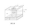
- FIG. 1Ais a cross section of a partially fabricated programmable conductor memory cell in an integrated circuit, constructed in accordance with a preferred embodiment of the present invention.
- FIG. 1Bis a perspective view of the partially fabricated programmable conductor memory cell of FIG. 1 A.
- FIG. 1Cis a cross section of a partially fabricated memory cell for an integrated circuit, constructed in accordance with another embodiment of the present invention.
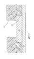
- FIG. 2is a cross section showing an embodiment of the current invention wherein an anode via has a smaller diameter than the memory cell body and is formed concentrically thereover.
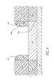
- FIG. 3is a cross section showing the programmable conductor memory cell of FIG. 1A after deposition of an insulating layer, formation of an anode via therein and deposition of conformal layer of silicon nitride, according to another embodiment of the current invention.
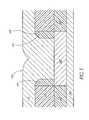
- FIG. 4is a cross section showing the programmable conductor memory cell of FIG. 3 after a spacer etch has been performed.
- FIG. 5is a cross section showing the structure of FIG. 3 , after a metal layer has been deposited into the spacer-lined anode via.
- a “programmable conductor” memory cell deviceincorporating a glass electrolyte element with an adjustable conductivity
- the amount of growth in a given switching timedepends, in part, on the availability of metal ions. Therefore, it is important that the cations come from a controlled source, such as from the solid solution of the cell body or glass electrolyte, which supplies an amount of cations proportional to the concentration therein and to the electric field. If additional cations are supplied from other, less reliable sources, the amount of cations may not be directly and reproducibly related to the strength of the electric field or switching time.
- the interface between the cell body sidewall and the surrounding insulating layercan provide a diffusion path for metal atoms and ions.
- a metal anode layere.g., silver
- the edgeshown in FIG. 1B as 115
- the anode viais designed to have the same width as the cell body via, even slight variations in mask registration can result in large differences in the contact area between the anode and the edge of the cell body sidewall, regardless of conventional mechanisms to minimize the effect of mask misalignment.
- the preferred embodimentsprovide means for avoiding differential contact area between the anode and the edge of the glass electrolyte element.
- a cathode layer 101which is connected to the negative pole of a power supply, is shown.
- the cathode layer 101comprises tungsten (W).
- An insulating layer 103preferably silicon nitride (Si 3 N 4 ) is deposited over the cathode layer 101 .
- the thick planarized insulating layer 103can comprise a form of silicon oxide, such as TEOS or BPSG, although it is preferred to define the sidewall with a material that prevents the diffusion of metal between devices.
- the thickness of the insulating layer 103is preferably between about 10 nm and 200 nm, more preferably between about 25 nm and 100 nm and most preferably about 50 nm.
- a cell body via 105is etched through the insulating layer 103 , opening a window to the cathode layer 101 , using standard patterning and etching techniques.
- the width of the cell body via 105is preferably between about 100 nm and 500 nm, more preferably between about 200 nm and 300 nm, and most preferably about 250 nm.
- the cell body via 105is filled with a glass electrolyte 107 (sometimes referred to in the literature as a Glass Fast Ion Diffusion or GFID element).
- FIG. 1Ba perspective view of the first components of the programmable conductor memory cell already seen in cross section in FIG. 1 A.
- the glass electrolyte element 107is shown embedded in the insulating layer 103 and making contact with an underlying cathode layer 101 .
- the sidewall 113 of the glass electrolyte elementis defined as the outer, cylindrical (in the illustrated embodiment) surface of the element, which is defined by the surrounding via wall 105 .
- the edge 115 of the sidewall 113is the intersection of the glass electrolyte element sidewall 113 and the top surface 109 . In the illustrated embodiment, the edge 115 of the sidewall 113 has the form of a circle.
- a ternary compoundsilver germanium selenide, which is a stable amorphous material.
- Silverconstitutes preferably between about 20% and 50%, more preferably between about 25% and 35% and most preferably about 30% (atomic percent) of the compound.
- the ternary compoundis a glass electrolyte material. The amount of silver formed over the glass is preferably selected to be completely consumed by the photodissolution process. After formation of the glass electrolyte material, the top surface 111 can be planarized again to remove any remaining metal.
- metal for the programmable conductor memoryis supplied by other means.
- a layer containing a mixture of tungsten-silver of about 50%—50% by weightcan be co-sputtered onto the glass electrolyte as a source of silver ions.
- the metal and glass materialcan be co-sputtered or deposited from a source that contains all species, so no metal deposition and drive-in steps are needed.
- a second insulating layer 121preferably silicon nitride, is deposited over the first insulating layer 103 .
- the thickness of the second insulating layer 121is preferably between about 50 nm and 200 nm, more preferably between about 80 nm and 150 nm and most preferably about 100 nm.
- An anode via 123is etched through the Si 3 N 4 directly over the cell body via, exposing the glass electrolyte element 107 .
- the width of the anode via 123 in insulating layer 121is smaller than the width of the cell body 107 in insulating layer 103 , preferably by between about 10 nm and 100 nm and more preferably by between about 10 nm and 60 nm.
- the anode via 123is positioned over the cell body 107 roughly concentrically, that is, so that the sidewall of anode via 123 is spaced from the sidewall of cell body 107 all the way around, and only a central portion of the cell body 107 is exposed.
- the anode via 123 and the cell body via 105have about the same size and are aligned directly over one another, in accordance with another embodiment of the invention. Methods known in the art can be used to avoid mask misalignment problems. Additionally, a thin blanket layer 125 of spacer material, preferably an insulating material and most preferably Si 3 N 4 , is deposited conformally over the insulating layer 121 and the anode via 123 .
- the spacer materialneed not be the same as the surrounding insulating layer, although it is preferably a barrier to metal diffusion, particularly to diffusion of the fast diffusing element incorporated into the cell body 107 and anode to be formed.
- the thickness of the spacer layer 125is preferably between about 5 nm and 50 nm and more preferably between about 5 nm and 30 nm.
- a spacer etchis performed, preferably by reactive ion etching (RIE), wherein horizontal portions 127 ( FIG. 3 ) of the spacer layer 125 are removed preferentially, leaving vertical portions of the spacer layer 125 relatively unaffected.
- FIG. 4shows the vertical portions of the spacer layer 125 that remain after RIE, leaving a the spacer 131 lining vertical surfaces of the anode via 123 .
- the spacer 131forms a continuous lining around the sidewall of the anode via 123 .
- the spacer 131is a cylindrical annulus with a rounded top edge, whose outer side surface is in contact with the sidewall of the anode via 123 .
- the metal depositionis shown for an anode via 123 with a spacer 131 .
- the anode via filling and overlying anode layercan be deposited in this same manner for the embodiment described with respect to FIG. 2 , having an anode via 123 that is narrow (compared to the cell body 107 ) without a spacer.
- the anodemakes contact with only a central portion of the memory cell body and not with the sidewall edges.
- the memoryhas two basic states: 0 and 1.
- the memory cellWhen there is no conductive path, the memory cell has high electrical resistance and reads as 0.
- the conductive pathshorts the memory cell body 107 , from the cathode 101 to the anode 133 , the resistance is low and the memory cell reads as 1.
- the change in resistance of the memory cell with and without a conductive pathcan be as much as two orders of magnitude, e.g., a change from Megaohms to milliohms. Reversing the polarity of the voltage reverses the formation of the conductive path, redissolving metal cations into the glass.
- the memory cellcan be programmed into as many as 3 or 4 states by setting the extent of the conductive path growth. These changes can be detected easily by the bit lines and word lines in a memory array, such that changing the extent of the conductive path can serve to change the state of the memory bit.
Landscapes
- Engineering & Computer Science (AREA)
- Manufacturing & Machinery (AREA)
- Semiconductor Memories (AREA)
Abstract
Description
This invention relates generally to memory devices for integrated circuits and more particularly to an anode contact for a programmable conductor random access memory (PCRAM) cell.
The digital memory chip most commonly used in computers and computer system components is the dynamic random access memory (DRAM), wherein voltage stored in capacitors represents digital bits of information. Electric power must be supplied to the capacitors to maintain the information because, without frequent refresh cycles, the stored charge dissipates, and the information is lost. Memories that require constant power are known as volatile memories.
Non-volatile memories do not need frequent refresh cycles to preserve their stored information, so they consume less power than volatile memories. The information stays in the memory even when the power is turned off. There are many applications where non-volatile memories are preferred or required, such as in lap-top and palm-top computers, cell phones or control systems of automobiles. Non-volatile memories include magnetic random access memories (MRAMs), erasable programmable read only memories (EPROMs) and variations thereof.
Another type of non-volatile memory is the programmable conductor or programmable metallization memory cell, which is described by Kozicki et al. in (U.S. Pat. No. 5,761,115; No. 5,914,893; and No. 6,084,796) and is incorporated by reference herein. The programmable conductor cell of Kozicki et al. (also referred to by Kozicki et al. as a “metal dendrite memory”) comprises a glass ion conductor, such as a chalcogenide-metal ion glass, and a plurality of electrodes disposed at the surface of the fast ion conductor and spaced a distance apart from one another. The glass/ion element shall be referred to herein as a “glass electrolyte” or, more generally, “cell body.” When a voltage is applied across the anode and cathode, a non-volatile conductive pathway (considered a sidewall “dendrite” by Kozicki et al.) grows from the cathode through or along the cell body towards the anode. The growth of the dendrite depends upon applied voltage and time; the higher the voltage, the faster the growth rate; the longer the time, the longer the dendrite. The dendrite can retract, re-dissolving the metal ions into the cell body, by reversing the polarity of the voltage at the electrodes.
In the case of a dielectric material, programmable capacitance between electrodes are programmed by the extent of dendrite growth. In the case of resistive material, programmable resistances are also programmed in accordance with the extent of dendrite growth. The resistance or capacitance of the cell thus changes with changing dendrite length. By completely shorting the glass electrolyte, the metal dendrite can cause a radical change in current flow through the cell, defining a different memory state.
For the proper functioning of a memory device incorporating such a chalcogenide-metal ion glass element, it is important that growth of the conductive pathway have a reproducible relationship to applied voltage. For device operation, multiple cells across an array should ideally have a consistent response to the signals they receive.
The current invention addresses the issue of consistent memory cell response by ensuring a uniform supply of metal ions for formation of a conductive pathway under applied voltage.
A programmable conductor memory cell for an integrated circuit is disclosed. In accordance with one aspect of the invention, the memory cell includes a memory cell body, formed from a glass electrolyte element having metal ions disposed therein, which fills a cell body via in a first insulating layer. A cathode is in contact with the cell body at the bottom of the cell body via. The second insulating layer, which overlies the first insulating layer and the cell body, has an anode via therein that is positioned concentrically over the memory cell body. The anode via is filled with anode material so that the anode contacts only a central portion of the anode surface of the memory cell body, which central portion is spaced inwardly from the sidewall of the memory cell body.
In a preferred embodiment, the anode via is lined with a spacer, preferably of insulating material, to ensure coverage of the sidewall edge of the memory cell body. In another embodiment, the anode via is formed using a mask with an opening smaller in width than the memory cell body and having the opening arranged concentrically over the memory cell body. In this way the sidewall edge of the memory cell body is covered by the second insulating layer.
The memory cell body can comprise a chalcogenide glass electrolyte material, preferably germanium-selenium, containing metal ions such as silver.
These and other aspects of the invention will be better understood from the description below and the appended drawings, which are meant to illustrate and not to limit the invention, and in which:
For proper functioning of a “programmable conductor” memory cell device, incorporating a glass electrolyte element with an adjustable conductivity, it is important that the conductive pathway growth in response to a particular applied voltage occurs reproducibly and consistently across an array. Low voltages cause slow growth, whereas higher voltages result in faster growth of the conductive path. The amount of growth in a given switching time depends, in part, on the availability of metal ions. Therefore, it is important that the cations come from a controlled source, such as from the solid solution of the cell body or glass electrolyte, which supplies an amount of cations proportional to the concentration therein and to the electric field. If additional cations are supplied from other, less reliable sources, the amount of cations may not be directly and reproducibly related to the strength of the electric field or switching time.
For example, the interface between the cell body sidewall and the surrounding insulating layer can provide a diffusion path for metal atoms and ions. When a metal anode layer (e.g., silver) is in contact with the edge (shown inFIG. 1B as115) of the cell body sidewall, i.e., where the sidewall makes contact with the anode surface, there is additional diffusion of metal cations along the sidewall, through the interface, to the growing conductive pathway. If the anode via is designed to have the same width as the cell body via, even slight variations in mask registration can result in large differences in the contact area between the anode and the edge of the cell body sidewall, regardless of conventional mechanisms to minimize the effect of mask misalignment. These differences in contact area lead to differences in the metal supply through the cell body/insulator interface to the growing conductive pathway. Thus, the extent of the conductive pathway formation would depend nor just on applied voltage and/or switching time, but also on the amount of meal leakage along the sidewall. Accordingly, the preferred embodiments provide means for avoiding differential contact area between the anode and the edge of the glass electrolyte element.
A preferred embodiment of the current invention can be described beginning with reference toFIG. 1A , wherein the first components of a simplified programmable conductor memory cell for an integrated circuit are shown. Acathode layer 101, which is connected to the negative pole of a power supply, is shown. Preferably, thecathode layer 101 comprises tungsten (W). An insulatinglayer 103, preferably silicon nitride (Si3N4) is deposited over thecathode layer 101. In other arrangements, it will be understood that the thick planarizedinsulating layer 103 can comprise a form of silicon oxide, such as TEOS or BPSG, although it is preferred to define the sidewall with a material that prevents the diffusion of metal between devices. The thickness of the insulatinglayer 103 is preferably between about 10 nm and 200 nm, more preferably between about 25 nm and 100 nm and most preferably about 50 nm. A cell body via105 is etched through the insulatinglayer 103, opening a window to thecathode layer 101, using standard patterning and etching techniques. The width of the cell body via105 is preferably between about 100 nm and 500 nm, more preferably between about 200 nm and 300 nm, and most preferably about 250 nm. The cell body via105 is filled with a glass electrolyte107 (sometimes referred to in the literature as a Glass Fast Ion Diffusion or GFID element). The illustrated cell body preferably includes a chalcogenide glass, more preferably a glass comprising germanium and selenium (Ge—Se) and most preferably, Ge4Se6, Ge3Se, or Ge2Se8, and additionally includes metal ions. The actual ratios of elements in thecell body 107 can vary and more complicated structures for thecell body 107 and are also contemplated, one of which is illustrated in FIG.1C and discussed below. Once the cell body via105 is filled, thetop surface 109 of the Ge—Se 107 is made level with thetop surface 111 of the insulatinglayer 103, preferably by chemical mechanical planarization. Preferably the height of the programmable conductor memory cell body between the cathode surface and the anode surface is in the range of about 25 nm to 100 nm.
Some aspects of the glass electrolyte element that are helpful for understanding the embodiments of the current invention are shown inFIG. 1B , a perspective view of the first components of the programmable conductor memory cell already seen in cross section in FIG.1A. Theglass electrolyte element 107 is shown embedded in the insulatinglayer 103 and making contact with anunderlying cathode layer 101. Thesidewall 113 of the glass electrolyte element is defined as the outer, cylindrical (in the illustrated embodiment) surface of the element, which is defined by the surrounding viawall 105. Theedge 115 of thesidewall 113 is the intersection of the glasselectrolyte element sidewall 113 and thetop surface 109. In the illustrated embodiment, theedge 115 of thesidewall 113 has the form of a circle.
In the illustrated embodiment, in order to supply metal ions to the Ge—Se glass, a thin layer (not shown) of metal or a combination of metals, including metal(s) from Group IB or Group IIB, more preferably, silver, copper or zinc, is preferably deposited over a recessedtop surface 109 of the fast ion conducting element and metal ions are driven into the glass. The thickness of the metal layer is between about 2 nm and 10 nm, more preferably between about 3 nm and 8 nm and most preferably about 5 nm. For example, silver (Ag) ions can be driven into the Ge—Se material by exposing an overlying Ag layer to ultraviolet radiation with a wavelength less than 50 nm or through plasma treatment. Preferably, there is enough silver available in the layer to form a ternary compound, silver germanium selenide, which is a stable amorphous material. Silver constitutes preferably between about 20% and 50%, more preferably between about 25% and 35% and most preferably about 30% (atomic percent) of the compound. The ternary compound is a glass electrolyte material. The amount of silver formed over the glass is preferably selected to be completely consumed by the photodissolution process. After formation of the glass electrolyte material, thetop surface 111 can be planarized again to remove any remaining metal.
In other arrangements, metal for the programmable conductor memory is supplied by other means. For example, a layer containing a mixture of tungsten-silver of about 50%—50% by weight can be co-sputtered onto the glass electrolyte as a source of silver ions. In still other arrangements, the metal and glass material can be co-sputtered or deposited from a source that contains all species, so no metal deposition and drive-in steps are needed.
Regardless of how formed, the cell body orglass electrolyte element 107, including metal ions diffused therein, serves as the memory cell body.
With reference toFIG. 2 , a second insulatinglayer 121, preferably silicon nitride, is deposited over the first insulatinglayer 103. The thickness of the second insulatinglayer 121 is preferably between about 50 nm and 200 nm, more preferably between about 80 nm and 150 nm and most preferably about 100 nm. An anode via123 is etched through the Si3N4directly over the cell body via, exposing theglass electrolyte element 107.
In some arrangements, metal deposition and drive-in steps can be performed after etching the anode via instead of before deposition of the second insulatinglayer 121 as described above.
In the embodiment ofFIG. 2 , the width of the anode via123 in insulatinglayer 121 is smaller than the width of thecell body 107 in insulatinglayer 103, preferably by between about 10 nm and 100 nm and more preferably by between about 10 nm and 60 nm. The anode via123 is positioned over thecell body 107 roughly concentrically, that is, so that the sidewall of anode via123 is spaced from the sidewall ofcell body 107 all the way around, and only a central portion of thecell body 107 is exposed.
Referring now toFIG. 3 , the anode via123 and the cell body via105 have about the same size and are aligned directly over one another, in accordance with another embodiment of the invention. Methods known in the art can be used to avoid mask misalignment problems. Additionally, athin blanket layer 125 of spacer material, preferably an insulating material and most preferably Si3N4, is deposited conformally over the insulatinglayer 121 and the anode via123. The skilled artisan will appreciate, in view of the disclosure herein, that the spacer material need not be the same as the surrounding insulating layer, although it is preferably a barrier to metal diffusion, particularly to diffusion of the fast diffusing element incorporated into thecell body 107 and anode to be formed. The thickness of thespacer layer 125 is preferably between about 5 nm and 50 nm and more preferably between about 5 nm and 30 nm.
Referring toFIG. 4 , a spacer etch is performed, preferably by reactive ion etching (RIE), wherein horizontal portions127 (FIG. 3 ) of thespacer layer 125 are removed preferentially, leaving vertical portions of thespacer layer 125 relatively unaffected.FIG. 4 shows the vertical portions of thespacer layer 125 that remain after RIE, leaving a thespacer 131 lining vertical surfaces of the anode via123. It will be understood that thespacer 131 forms a continuous lining around the sidewall of the anode via123. In the illustrated embodiment, thespacer 131 is a cylindrical annulus with a rounded top edge, whose outer side surface is in contact with the sidewall of the anode via123.
Next, as shown inFIG. 5 , ametal anode layer 133, preferably including a metal or combination of metals from Group IB or Group IIB, more preferably copper or zinc and most preferably silver, is deposited. Preferably, themetal anode layer 133 is deposited so that it fills the anode via123 and forms aportion 135 overlying the second insulatinglayer 121 all as one contiguous body of material. Theoverlying portion 135 is subsequently patterned and etched as desired, depending upon the circuit design of the memory array.
InFIG. 5 , the metal deposition is shown for an anode via123 with aspacer 131. The anode via filling and overlying anode layer can be deposited in this same manner for the embodiment described with respect toFIG. 2 , having an anode via123 that is narrow (compared to the cell body107) without a spacer. In both the embodiment of FIG.2 and the embodiment ofFIG. 4 , the anode makes contact with only a central portion of the memory cell body and not with the sidewall edges.
When a voltage is applied across thelower electrode 101 andupper electrode 133, a conductive path forms between the cathode101 (i.e., the electrode connected to the negative pole of the power supply) and the anode133 (i.e., the electrode connected to the positive pole of the power supply). Without being limited by theory, it is believed that the conductive path grows by precipitation of cations (e.g., silver cations) from thememory cell body 107. Changes in the extent of the conductive path affect the overall resistance of the device. The conductive path tends to remain intact when the voltage is removed.
For a binary programmable conductor memory device, the memory has two basic states: 0 and 1. When there is no conductive path, the memory cell has high electrical resistance and reads as 0. When the conductive path shorts thememory cell body 107, from thecathode 101 to theanode 133, the resistance is low and the memory cell reads as 1. The change in resistance of the memory cell with and without a conductive path can be as much as two orders of magnitude, e.g., a change from Megaohms to milliohms. Reversing the polarity of the voltage reverses the formation of the conductive path, redissolving metal cations into the glass.
Alternatively, the memory cell can be programmed into as many as 3 or 4 states by setting the extent of the conductive path growth. These changes can be detected easily by the bit lines and word lines in a memory array, such that changing the extent of the conductive path can serve to change the state of the memory bit.
Thus, in one embodiment of the current invention, an anode via is made smaller than the cell body via so that the overlying insulator layer covers the cell body/insulator interface. The smaller anode vias are positioned so that their bottoms make contact only with the cell body and do not extend to the cell body/insulator interface. In another embodiment, a spacer prevents contact between the anode material and the cell body/insulator interface by covering the interface with spacer material near the outer edge of the anode via bottom. The preferred embodiments thus give reliable control to the spacing between the edge of the anode and the edge of the memory cell body or GFID material. These structures ensure that the anode cations that precipitate out to form the conductive path are those that were intentionally and controllably provide provided to the glass electrolyte material, whether by photodissolution, separate metal-containing layer (see FIG.1C), co-deposition or any other manner of metal doping. Silver content dissolved within a GeSe glass, for example, is self limiting at about 30 atm %, thus providing a reliably consistent source of diffusion ions for selectively forming the conductive path. For a given cation (e.g., Ag) concentration in solution, this provides conductive pathway formation reproducibly dependent upon voltage applied across the electrodes and/or switching time.
Although the embodiments of the invention have been described in the context of a vertically built device, one of skill in the art will recognize that this is not the only possible configuration or method for constructing a programmable conductor memory cell.
Claims (37)
1. A programmable conductor memory cell for an integrated circuit, comprising:
a first insulating layer having a top surface and a cell body via;
a memory cell body comprising a glass electrolyte with metal ions disposed therein, the memory cell body being contained within the cell body via and defining a sidewall where the memory cell body and the first insulating layer make contact;
a cathode in contact with the memory cell body;
a second insulating layer over the first insulating layer and defining an anode via to said the memory cell body;
an anode in contact with a top surface of the memory cell body and formed in the anode via;
wherein the anode contacts the top surface of the memory cell body without contacting the sidewall of the memory cell body, the anode via has a width about the same as a width of the memory cell body, and the anode via is lined with a spacer that covers an edge of the sidewall of the memory cell body.
2. The programmable conductor memory cell ofclaim 1 wherein the spacer comprises an insulating material.
3. The programmable conductor memory cell ofclaim 1 wherein the spacer has a thickness extending into the anode via between about 5 nm and 30 nm.
4. The programmable conductor memory cell ofclaim 1 wherein the spacer comprises silicon nitride.
5. The programmable conductor memory cell ofclaim 1 wherein the anode via is filled with metal.
6. The programmable conductor memory cell ofclaim 5 wherein the metal is contiguous with a metal layer over the second insulating layer.
7. The programmable conductor memory cell ofclaim 1 wherein the cathode comprises tungsten.
8. The programmable conductor memory cell ofclaim 1 wherein the memory cell body comprises a chalcogenide-metal ion glass electrolyte material.
9. The programmable conductor memory cell ofclaim 8 wherein the metal ions are chosen from the group consisting of silver, copper, zinc and combinations thereof.
10. The programmable conductor memory cell ofclaim 8 wherein the anode comprises silver.
11. The programmable conductor memory cell ofclaim 10 wherein the glass electrolyte material comprises silver-germanium-selenium.
12. The programmable conductor memory cell ofclaim 1 wherein a distance between a bottom surface and the top surface of the memory cell body is about 25 nm to 100 nm.
13. The programmable conductor memory cell ofclaim 1 wherein a width of the cell body via is between about 100 nm and 500 nm.
14. The programmable conductor memory cell ofclaim 1 wherein a width of the cell body via is between about 200 nm and 300 nm.
15. The programmable conductor memory cell ofclaim 1 wherein the first insulating layer comprises silicon nitride.
16. The programmable conductor memory cell ofclaim 15 wherein the first insulating layer has a thickness between about 10 nm and 200 nm.
17. The programmable conductor memory cell ofclaim 15 wherein the first insulating layer has a thickness between about 25 nm and 150 nm.
18. The programmable conductor memory cell ofclaim 1 wherein the second insulating layer comprises silicon nitride.
19. The programmable conductor memory cell ofclaim 18 wherein the second insulating layer has a thickness between about 50 nm and 200 nm.
20. The programmable conductor memory cell ofclaim 18 wherein the second insulating layer has a thickness between about 80 nm and 150 nm.
21. The programmable conductor memory cell ofclaim 1 wherein the anode via has a width no greater than a width of the cell body via.
22. The programmable conductor memory cell ofclaim 1 , wherein the memory cell body fills the cell body via.
23. The programmable conductor memory cell ofclaim 1 , wherein the top surface of the memory cell body is coplanar with the top surface of the first insulating layer.
24. The programmable conductor memory cell ofclaim 1 , wherein the cathode extends outside the sidewall of the memory cell body.
25. A programmable conductor random access memory cell, comprising:
a cathode;
a first insulating layer over the cathode and defining a via to the cathode;
a silver-germanium-selenium glass electrolyte memory cell body in the via and over the cathode, the cathode extending beyond a sidewall of the memory cell body;
a second insulating layer over the first insulating layer, having an anode via to the memory cell body;
a spacer lining the anode via; and
an anode within said the spacer lining the anode via in contact with the memory cell body.
26. The programmable conductor memory cell ofclaim 25 wherein the spacer comprises an insulating material.
27. The programmable conductor memory cell ofclaim 26 wherein the spacer comprises silicon nitride.
28. The programmable conductor memory cell ofclaim 27 wherein a thickness of the spacer is between about 5 nm and 30 nm.
29. The programmable conductor memory cell ofclaim 25 , wherein the anode is silver.
30. The programmable conductor memory cell ofclaim 25 , wherein the memory cell body comprises a layer of GexSe10-x, x being about 4, and a layer of silver selenide.
31. A programmable conductor random access memory cell comprising:
an upper insulating layer having an anode via, the anode via having a sidewall;
insulating material along the sidewall and narrowing the anode via;
an anode contained by the narrowed anode via and overlying the upper insulating layer;
a lower insulating layer having a cell body via; and
a memory cell body within the cell body via and having a sidewall edge, the anode contacting the memory cell body without contacting the sidewall edge, the memory cell body comprising a germanium selenide layer and a silver selenide layer.
32. A programmable conductor random access memory cell comprising:
an insulating layer;
an anode in an anode via through the insulating layer, the anode filling the anode via; and
a glass electrolyte element, the anode making contact with only a central portion of an upper surface of the glass electrolyte element, the glass electrolyte element including a layer of GexSe10-x, x being about 4, and a layer of silver selenide.
33. The programmable conductor memory cell ofclaim 32 wherein the anode comprises silver.
34. The programmable conductor memory cell ofclaim 32 , wherein the anode is a metal.
35. A The programmable conductor memory cell for an integrated circuit, comprising:
a first insulating layer having a top surface and a cell body via;
a memory cell body comprising a glass electrolyte with metal ions disposed therein, the memory cell body being contained within the cell body via and defining a sidewall where the memory cell body and the first insulating layer make contact;
a cathode in contact with the memory cell body;
a second insulating layer over the first insulating layer and defining an anode via to the memory cell body;
an anode in contact with a top surface of the memory cell body and formed in the anode via;
wherein the anode contacts the top surface of the memory cell body without contacting the sidewall of the memory cell body, and the memory cell body comprises a layer of GexSe10-x, x being about4, and a layer of silver selenide.
36. The programmable conductor memory cell ofclaim 35 wherein the anode via is smaller in width than the memory cell body, and a sidewall edge of the memory cell body is covered by the second insulating layer.
37. The programmable conductor memory cell ofclaim 35 wherein the second insulating layer comprises silicon nitride.
Priority Applications (4)
| Application Number | Priority Date | Filing Date | Title |
|---|---|---|---|
| US10/121,790US6864500B2 (en) | 2002-04-10 | 2002-04-10 | Programmable conductor memory cell structure |
| US10/618,824US6838307B2 (en) | 2002-04-10 | 2003-07-14 | Programmable conductor memory cell structure and method therefor |
| US10/787,123US7132675B2 (en) | 2002-04-10 | 2004-02-27 | Programmable conductor memory cell structure and method therefor |
| US11/435,824US7547905B2 (en) | 2002-04-10 | 2006-05-18 | Programmable conductor memory cell structure and method therefor |
Applications Claiming Priority (1)
| Application Number | Priority Date | Filing Date | Title |
|---|---|---|---|
| US10/121,790US6864500B2 (en) | 2002-04-10 | 2002-04-10 | Programmable conductor memory cell structure |
Related Child Applications (2)
| Application Number | Title | Priority Date | Filing Date |
|---|---|---|---|
| US10/618,824DivisionUS6838307B2 (en) | 2002-04-10 | 2003-07-14 | Programmable conductor memory cell structure and method therefor |
| US10/787,123ContinuationUS7132675B2 (en) | 2002-04-10 | 2004-02-27 | Programmable conductor memory cell structure and method therefor |
Publications (2)
| Publication Number | Publication Date |
|---|---|
| US20030193059A1 US20030193059A1 (en) | 2003-10-16 |
| US6864500B2true US6864500B2 (en) | 2005-03-08 |
Family
ID=28790403
Family Applications (4)
| Application Number | Title | Priority Date | Filing Date |
|---|---|---|---|
| US10/121,790Expired - LifetimeUS6864500B2 (en) | 2002-04-10 | 2002-04-10 | Programmable conductor memory cell structure |
| US10/618,824Expired - LifetimeUS6838307B2 (en) | 2002-04-10 | 2003-07-14 | Programmable conductor memory cell structure and method therefor |
| US10/787,123Expired - LifetimeUS7132675B2 (en) | 2002-04-10 | 2004-02-27 | Programmable conductor memory cell structure and method therefor |
| US11/435,824Expired - LifetimeUS7547905B2 (en) | 2002-04-10 | 2006-05-18 | Programmable conductor memory cell structure and method therefor |
Family Applications After (3)
| Application Number | Title | Priority Date | Filing Date |
|---|---|---|---|
| US10/618,824Expired - LifetimeUS6838307B2 (en) | 2002-04-10 | 2003-07-14 | Programmable conductor memory cell structure and method therefor |
| US10/787,123Expired - LifetimeUS7132675B2 (en) | 2002-04-10 | 2004-02-27 | Programmable conductor memory cell structure and method therefor |
| US11/435,824Expired - LifetimeUS7547905B2 (en) | 2002-04-10 | 2006-05-18 | Programmable conductor memory cell structure and method therefor |
Country Status (1)
| Country | Link |
|---|---|
| US (4) | US6864500B2 (en) |
Cited By (168)
| Publication number | Priority date | Publication date | Assignee | Title |
|---|---|---|---|---|
| US20050226062A1 (en)* | 2003-03-20 | 2005-10-13 | Sony Corporation | Memory element and storage device using this |
| US20060110878A1 (en)* | 2004-11-22 | 2006-05-25 | Macronix International Co., Ltd. | Side wall active pin memory and manufacturing method |
| US20060124916A1 (en)* | 2004-12-09 | 2006-06-15 | Macronix International Co., Ltd. | Self-aligned small contact phase-change memory method and device |
| US20060208249A1 (en)* | 2002-04-10 | 2006-09-21 | Micron Technology, Inc. | Programmable conductor memory cell structure and method therefor |
| US20060284158A1 (en)* | 2005-06-17 | 2006-12-21 | Macronix International Co., Ltd. | Self-aligned, embedded phase change ram and manufacturing method |
| US20060284085A1 (en)* | 2004-07-20 | 2006-12-21 | Minhwan Lee | Electrochemical nano-patterning using ionic conductors |
| US20060286743A1 (en)* | 2005-06-17 | 2006-12-21 | Macronix International Co., Ltd. | Method for Manufacturing a Narrow Structure on an Integrated Circuit |
| US20060284214A1 (en)* | 2005-06-17 | 2006-12-21 | Macronix International Co., Ltd. | Thin film fuse phase change cell with thermal isolation layer and manufacturing method |
| US20060284157A1 (en)* | 2005-06-17 | 2006-12-21 | Macronix International Co., Ltd. | Thin film plate phase change RAM circuit and manufacturing method |
| US20070108430A1 (en)* | 2005-11-15 | 2007-05-17 | Macronix International Co., Ltd. | Thermally contained/insulated phase change memory device and method (combined) |
| US20070108429A1 (en)* | 2005-11-14 | 2007-05-17 | Macronix International Co., Ltd. | Pipe shaped phase change memory |
| US20070109843A1 (en)* | 2005-11-15 | 2007-05-17 | Macronix International Co., Ltd. | Phase Change Memory Device and Manufacturing Method |
| US20070117315A1 (en)* | 2005-11-22 | 2007-05-24 | Macronix International Co., Ltd. | Memory cell device and manufacturing method |
| US20070121363A1 (en)* | 2005-11-28 | 2007-05-31 | Macronix International Co., Ltd. | Phase Change Memory Cell and Manufacturing Method |
| US20070126040A1 (en)* | 2005-11-21 | 2007-06-07 | Hsiang-Lan Lung | Vacuum cell thermal isolation for a phase change memory device |
| US20070131922A1 (en)* | 2005-12-13 | 2007-06-14 | Macronix International Co., Ltd. | Thin Film Fuse Phase Change Cell with Thermal Isolation Pad and Manufacturing Method |
| US20070131980A1 (en)* | 2005-11-21 | 2007-06-14 | Lung Hsiang L | Vacuum jacket for phase change memory element |
| US20070155172A1 (en)* | 2005-12-05 | 2007-07-05 | Macronix International Co., Ltd. | Manufacturing Method for Phase Change RAM with Electrode Layer Process |
| US20070158633A1 (en)* | 2005-12-27 | 2007-07-12 | Macronix International Co., Ltd. | Method for Forming Self-Aligned Thermal Isolation Cell for a Variable Resistance Memory Array |
| US20070158690A1 (en)* | 2006-01-09 | 2007-07-12 | Macronix International Co., Ltd. | Programmable Resistive RAM and Manufacturing Method |
| US20070158645A1 (en)* | 2006-01-11 | 2007-07-12 | Macronix International Co., Ltd. | Self-align planerized bottom electrode phase change memory and manufacturing method |
| US20070161186A1 (en)* | 2006-01-09 | 2007-07-12 | Macronix International Co., Ltd. | Programmable Resistive RAM and Manufacturing Method |
| US20070158632A1 (en)* | 2006-01-09 | 2007-07-12 | Macronix International Co., Ltd. | Method for Fabricating a Pillar-Shaped Phase Change Memory Element |
| US20070158862A1 (en)* | 2005-11-21 | 2007-07-12 | Hsiang-Lan Lung | Vacuum jacketed electrode for phase change memory element |
| US20070173019A1 (en)* | 2006-01-09 | 2007-07-26 | Macronix International Co., Ltd. | Programmable Resistive Ram and Manufacturing Method |
| US20070173063A1 (en)* | 2006-01-24 | 2007-07-26 | Macronix International Co., Ltd. | Self-aligned manufacturing method, and manufacturing method for thin film fuse phase change ram |
| US20070176261A1 (en)* | 2006-01-30 | 2007-08-02 | Macronix International Co., Ltd. | Vertical Side Wall Active Pin Structures in a Phase Change Memory and Manufacturing Methods |
| US20070241371A1 (en)* | 2006-04-17 | 2007-10-18 | Macronix International Co., Ltd. | Memory device and manufacturing method |
| US20070257300A1 (en)* | 2006-05-05 | 2007-11-08 | Macronix International Co., Ltd. | Structures and Methods of a Bistable Resistive Random Access Memory |
| US20070262388A1 (en)* | 2006-05-09 | 2007-11-15 | Macronix International Co., Ltd. | Bridge Resistance Random Access Memory Device and Method With A Singular Contact Structure |
| US20070274121A1 (en)* | 2005-06-17 | 2007-11-29 | Macronix International Co., Ltd. | Multi-level memory cell having phase change element and asymmetrical thermal boundary |
| US20070281420A1 (en)* | 2006-05-30 | 2007-12-06 | Macronix International Co., Ltd. | Resistor random access memory cell with reduced active area and reduced contact areas |
| US20070278529A1 (en)* | 2006-05-30 | 2007-12-06 | Macronix International Co., Ltd. | Resistor random access memory cell with l-shaped electrode |
| US20070287252A1 (en)* | 2006-06-09 | 2007-12-13 | Micron Technology, Inc. | Methods of forming variable resistance memory cells, and methods of etching germanium, antimony, and tellurium-comprising materials |
| US20080014676A1 (en)* | 2006-07-12 | 2008-01-17 | Macronix International Co., Ltd. | Method for Making a Pillar-Type Phase Change Memory Element |
| US7321130B2 (en) | 2005-06-17 | 2008-01-22 | Macronix International Co., Ltd. | Thin film fuse phase change RAM and manufacturing method |
| US20080031043A1 (en)* | 2006-07-05 | 2008-02-07 | Hideaki Aochi | Non-volatile memory device |
| US20080043520A1 (en)* | 2006-02-07 | 2008-02-21 | Chen Shih H | I-shaped phase change memory cell with thermal isolation |
| US20080061341A1 (en)* | 2006-09-11 | 2008-03-13 | Macronix International Co., Ltd. | Memory Device Having Wide Area Phase Change Element and Small Electrode Contact Area |
| US20080096341A1 (en)* | 2006-10-24 | 2008-04-24 | Macronix International Co., Ltd. | Method for Manufacturing a Resistor Random Access Memory with Reduced Active Area and Reduced Contact Areas |
| US20080096375A1 (en)* | 2006-10-18 | 2008-04-24 | Macronix International Co., Ltd. | Method for Making Memory Cell Device |
| US20080094885A1 (en)* | 2006-10-24 | 2008-04-24 | Macronix International Co., Ltd. | Bistable Resistance Random Access Memory Structures with Multiple Memory Layers and Multilevel Memory States |
| US20080099791A1 (en)* | 2006-10-04 | 2008-05-01 | Macronix International Co., Ltd. | Memory Cell Device with Circumferentially-Extending Memory Element |
| US20080106923A1 (en)* | 2006-10-24 | 2008-05-08 | Macronix International Co., Ltd. | Phase Change Memory Cells with Dual Access Devices |
| US20080116440A1 (en)* | 2006-11-16 | 2008-05-22 | Macronix International Co., Ltd. | Resistance Random Access Memory Structure for Enhanced Retention |
| US20080121861A1 (en)* | 2006-08-16 | 2008-05-29 | Macronix International Co., Ltd. | Self-Aligned Structure and Method for Confining a Melting Point in a Resistor Random Access Memory |
| US7385235B2 (en) | 2002-08-09 | 2008-06-10 | Macronix International Co., Ltd. | Spacer chalcogenide memory device |
| US20080137400A1 (en)* | 2006-12-06 | 2008-06-12 | Macronix International Co., Ltd. | Phase Change Memory Cell with Thermal Barrier and Method for Fabricating the Same |
| US20080138931A1 (en)* | 2006-12-06 | 2008-06-12 | Macronix International Co., Ltd. | Method for Making a Self-Converged Void and Bottom Electrode for Memoery Cell |
| US20080138929A1 (en)* | 2006-12-06 | 2008-06-12 | Macronix International Co., Ltd. | Method for Making a Self-Converged Memory Material Element for Memory Cell |
| US20080135824A1 (en)* | 2006-12-07 | 2008-06-12 | Macronix International Co., Ltd. | Method and Structure of a Multi-Level Cell Resistance Random Access Memory with Metal Oxides |
| US7388771B2 (en) | 2006-10-24 | 2008-06-17 | Macronix International Co., Ltd. | Methods of operating a bistable resistance random access memory with multiple memory layers and multilevel memory states |
| US20080142984A1 (en)* | 2006-12-15 | 2008-06-19 | Macronix International Co., Ltd. | Multi-Layer Electrode Structure |
| US20080144353A1 (en)* | 2006-12-13 | 2008-06-19 | Macronix International Co., Ltd. | Method, Apparatus and Computer Program Product for Read Before Programming Process on Programmable Resistive Memory Cell |
| US20080157053A1 (en)* | 2006-12-28 | 2008-07-03 | Macronix International Co., Ltd. | Resistor Random Access Memory Cell Device |
| US20080165571A1 (en)* | 2007-01-09 | 2008-07-10 | Macronix International Co., Ltd. | Method, Apparatus and Computer Program Product for Read Before Programming Process on Multiple Programmable Resistive Memory Cell |
| US20080165570A1 (en)* | 2007-01-05 | 2008-07-10 | Macronix International Co., Ltd. | Current Compliant Sensing Architecture for Multilevel Phase Change Memory |
| US20080186755A1 (en)* | 2007-02-05 | 2008-08-07 | Macronix International Co., Ltd. | Memory cell device and programming methods |
| US20080186761A1 (en)* | 2007-02-07 | 2008-08-07 | Macronix International Co., Ltd. | Memory Cell with Separate Read and Program Paths |
| US20080185730A1 (en)* | 2007-02-02 | 2008-08-07 | Macronix International Co., Ltd. | Memory cell device with coplanar electrode surface and method |
| US20080191187A1 (en)* | 2007-02-12 | 2008-08-14 | Macronix International Co., Ltd. | Method for manufacturing a phase change memory device with pillar bottom electrode |
| US20080192534A1 (en)* | 2007-02-08 | 2008-08-14 | Macronix International Co., Ltd. | Memory element with reduced-current phase change element |
| US20080191186A1 (en)* | 2007-02-14 | 2008-08-14 | Macronix International Co., Ltd. | Phase change memory cell with filled sidewall memory element and method for fabricating the same |
| US7414258B2 (en) | 2005-11-16 | 2008-08-19 | Macronix International Co., Ltd. | Spacer electrode small pin phase change memory RAM and manufacturing method |
| US20080197333A1 (en)* | 2007-02-21 | 2008-08-21 | Macronix International Co., Ltd. | Programmable Resistive Memory Cell with Self-Forming Gap |
| US20080197334A1 (en)* | 2007-02-21 | 2008-08-21 | Macronix International Co., Ltd. | Phase Change Memory Cell with Heater and Method for Fabricating the Same |
| US20080203375A1 (en)* | 2007-02-27 | 2008-08-28 | Macronix International Co., Ltd. | Memory Cell with Memory Element Contacting Ring-Shaped Upper End of Bottom Electrode |
| US7423300B2 (en) | 2006-05-24 | 2008-09-09 | Macronix International Co., Ltd. | Single-mask phase change memory element |
| US20080247224A1 (en)* | 2007-04-06 | 2008-10-09 | Macronix International Co., Ltd. | Phase Change Memory Bridge Cell with Diode Isolation Device |
| US7440315B2 (en) | 2007-01-09 | 2008-10-21 | Macronix International Co., Ltd. | Method, apparatus and computer program product for stepped reset programming process on programmable resistive memory cell |
| US20080259672A1 (en)* | 2007-04-17 | 2008-10-23 | Macronix International Co., Ltd. | 4f2 self align side wall active phase change memory |
| US20080266933A1 (en)* | 2007-04-24 | 2008-10-30 | Macronix International Co., Ltd. | Method and Apparatus for Refreshing Programmable Resistive Memory |
| US20080266940A1 (en)* | 2005-11-21 | 2008-10-30 | Erh-Kun Lai | Air Cell Thermal Isolation for a Memory Array Formed of a Programmable Resistive Material |
| US7450411B2 (en) | 2005-11-15 | 2008-11-11 | Macronix International Co., Ltd. | Phase change memory device and manufacturing method |
| KR100870054B1 (en)* | 2005-03-16 | 2008-11-24 | 인피니언 테크놀로지스 아게 | Solid electrolyte memory element and method for fabricating such a memory element |
| US20090014706A1 (en)* | 2007-07-13 | 2009-01-15 | Macronix International Co., Ltd. | 4f2 self align fin bottom electrodes fet drive phase change memory |
| US20090034323A1 (en)* | 2007-08-02 | 2009-02-05 | Macronix International Co., Ltd. | Phase change memory with dual word lines and source lines and method of operating same |
| US20090032796A1 (en)* | 2007-07-31 | 2009-02-05 | Macronix International Co., Ltd. | Phase change memory bridge cell |
| US20090032793A1 (en)* | 2007-08-03 | 2009-02-05 | Macronix International Co., Ltd. | Resistor Random Access Memory Structure Having a Defined Small Area of Electrical Contact |
| US20090072215A1 (en)* | 2007-09-14 | 2009-03-19 | Macronix International Co., Ltd. | Phase change memory cell in via array with self-aligned, self-converged bottom electrode and method for manufacturing |
| US20090072216A1 (en)* | 2007-09-14 | 2009-03-19 | Macronix International Co., Ltd. | Phase change memory cell array with self-converged bottom electrode and method for manufacturing |
| US7507986B2 (en) | 2005-11-21 | 2009-03-24 | Macronix International Co., Ltd. | Thermal isolation for an active-sidewall phase change memory cell |
| US20090095948A1 (en)* | 2007-10-12 | 2009-04-16 | Macronix International Co., Ltd. | Programmable Resistive Memory with Diode Structure |
| US7521364B2 (en) | 2005-12-02 | 2009-04-21 | Macronix Internation Co., Ltd. | Surface topology improvement method for plug surface areas |
| US20090122588A1 (en)* | 2007-11-14 | 2009-05-14 | Macronix International Co., Ltd. | Phase change memory cell including a thermal protect bottom electrode and manufacturing methods |
| US7534647B2 (en) | 2005-06-17 | 2009-05-19 | Macronix International Co., Ltd. | Damascene phase change RAM and manufacturing method |
| US7535756B2 (en) | 2007-01-31 | 2009-05-19 | Macronix International Co., Ltd. | Method to tighten set distribution for PCRAM |
| US20090147564A1 (en)* | 2007-12-07 | 2009-06-11 | Macronix International Co., Ltd. | Phase change memory cell having interface structures with essentially equal thermal impedances and manufacturing methods |
| US20090184310A1 (en)* | 2008-01-18 | 2009-07-23 | Macronix International Co., Ltd. | Memory cell with memory element contacting an inverted t-shaped bottom electrode |
| US20090189138A1 (en)* | 2008-01-28 | 2009-07-30 | Macronix International Co., Ltd. | Fill-in etching free pore device |
| US7569844B2 (en) | 2007-04-17 | 2009-08-04 | Macronix International Co., Ltd. | Memory cell sidewall contacting side electrode |
| US20090242880A1 (en)* | 2008-03-25 | 2009-10-01 | Macronix International Co., Ltd. | Thermally stabilized electrode structure |
| US20090261313A1 (en)* | 2008-04-22 | 2009-10-22 | Macronix International Co., Ltd. | Memory cell having a buried phase change region and method for fabricating the same |
| US20090279350A1 (en)* | 2008-05-07 | 2009-11-12 | Macronix International Co., Ltd. | Bipolar switching of phase change device |
| US20090309087A1 (en)* | 2008-06-12 | 2009-12-17 | Macronix International Co., Ltd. | Phase change memory cell having top and bottom sidewall contacts |
| US7635855B2 (en) | 2005-11-15 | 2009-12-22 | Macronix International Co., Ltd. | I-shaped phase change memory cell |
| US7639527B2 (en) | 2008-01-07 | 2009-12-29 | Macronix International Co., Ltd. | Phase change memory dynamic resistance test and manufacturing methods |
| US20100019215A1 (en)* | 2008-07-22 | 2010-01-28 | Macronix International Co., Ltd. | Mushroom type memory cell having self-aligned bottom electrode and diode access device |
| US7663135B2 (en) | 2007-01-31 | 2010-02-16 | Macronix International Co., Ltd. | Memory cell having a side electrode contact |
| US20100046285A1 (en)* | 2008-08-19 | 2010-02-25 | Macronix International Co., Ltd. | Multiple phase change materials in an integrated circuit for system on a chip application |
| US20100067285A1 (en)* | 2008-09-12 | 2010-03-18 | Macronix International Co., Ltd. | Novel sensing circuit for pcram applications |
| US7682868B2 (en) | 2006-12-06 | 2010-03-23 | Macronix International Co., Ltd. | Method for making a keyhole opening during the manufacture of a memory cell |
| US7688619B2 (en) | 2005-11-28 | 2010-03-30 | Macronix International Co., Ltd. | Phase change memory cell and manufacturing method |
| US20100084624A1 (en)* | 2008-10-02 | 2010-04-08 | Macronix International Co., Ltd. | Dielectric mesh isolated phase change structure for phase change memory |
| US7696506B2 (en) | 2006-06-27 | 2010-04-13 | Macronix International Co., Ltd. | Memory cell with memory material insulation and manufacturing method |
| US20100091558A1 (en)* | 2008-10-10 | 2010-04-15 | Macronix International Co., Ltd. | Dielectric-Sandwiched Pillar Memory Device |
| US7701750B2 (en) | 2008-05-08 | 2010-04-20 | Macronix International Co., Ltd. | Phase change device having two or more substantial amorphous regions in high resistance state |
| US20100110778A1 (en)* | 2008-11-06 | 2010-05-06 | Macronix International Co., Ltd. | Phase change memory program method without over-reset |
| US20100117048A1 (en)* | 2008-11-07 | 2010-05-13 | Macronix International Co., Ltd. | Memory cell access device having a pn-junction with polycrystalline and single-crystal semiconductor regions |
| US20100157688A1 (en)* | 2008-12-23 | 2010-06-24 | Actel Corporation | Push-pull memory cell configured for simultaneous programming of n-channel and p-channel non-volatile transistors |
| US20100171086A1 (en)* | 2009-01-07 | 2010-07-08 | Macronix International Co., Ltd. | Integrated circuit memory with single crystal silicon on silicide driver and manufacturing method |
| US20100177559A1 (en)* | 2009-01-12 | 2010-07-15 | Macronix International Co., Ltd. | Method for setting pcram devices |
| US20100176362A1 (en)* | 2009-01-13 | 2010-07-15 | Macronix International Co., Ltd. | Polysilicon plug bipolar transistor for phase change memory |
| US7777215B2 (en) | 2007-07-20 | 2010-08-17 | Macronix International Co., Ltd. | Resistive memory structure with buffer layer |
| US20100208520A1 (en)* | 2009-02-13 | 2010-08-19 | Actel Corporation | Array and control method for flash based fpga cell |
| US7786461B2 (en) | 2007-04-03 | 2010-08-31 | Macronix International Co., Ltd. | Memory structure with reduced-size memory element between memory material portions |
| US20100270529A1 (en)* | 2009-04-27 | 2010-10-28 | Macronix International Co., Ltd. | Integrated circuit 3d phase change memory array and manufacturing method |
| US7825479B2 (en) | 2008-08-06 | 2010-11-02 | International Business Machines Corporation | Electrical antifuse having a multi-thickness dielectric layer |
| US7825398B2 (en) | 2008-04-07 | 2010-11-02 | Macronix International Co., Ltd. | Memory cell having improved mechanical stability |
| US20100276654A1 (en)* | 2009-04-30 | 2010-11-04 | Macronix International Co., Ltd. | Low Operational Current Phase Change Memory Structures |
| US20100290271A1 (en)* | 2009-05-15 | 2010-11-18 | Macronix International Co., Ltd. | One-transistor, one-resistor, one-capacitor phase change memory |
| US20100295123A1 (en)* | 2009-05-22 | 2010-11-25 | Macronix International Co., Ltd. | Phase Change Memory Cell Having Vertical Channel Access Transistor |
| US20100314601A1 (en)* | 2009-06-15 | 2010-12-16 | Macronix International Co., Ltd. | Phase change memory having stabilized microstructure and manufacturing method |
| US20110001108A1 (en)* | 2009-07-02 | 2011-01-06 | Actel Corporation | Front to back resistive random access memory cells |
| US7869270B2 (en) | 2008-12-29 | 2011-01-11 | Macronix International Co., Ltd. | Set algorithm for phase change memory cell |
| US20110024821A1 (en)* | 2008-12-12 | 2011-02-03 | Actel Corporation | Push-pull fpga cell |
| US7894254B2 (en) | 2009-07-15 | 2011-02-22 | Macronix International Co., Ltd. | Refresh circuitry for phase change memory |
| US7910907B2 (en) | 2006-03-15 | 2011-03-22 | Macronix International Co., Ltd. | Manufacturing method for pipe-shaped electrode phase change memory |
| US20110076824A1 (en)* | 2009-09-30 | 2011-03-31 | Hynix Semiconductor Inc. | Fabrication method of phase change random access memory device |
| US7919766B2 (en) | 2007-10-22 | 2011-04-05 | Macronix International Co., Ltd. | Method for making self aligning pillar memory cell device |
| US7928421B2 (en) | 2006-04-21 | 2011-04-19 | Macronix International Co., Ltd. | Phase change memory cell with vacuum spacer |
| US7932506B2 (en) | 2008-07-22 | 2011-04-26 | Macronix International Co., Ltd. | Fully self-aligned pore-type memory cell having diode access device |
| US8030634B2 (en) | 2008-03-31 | 2011-10-04 | Macronix International Co., Ltd. | Memory array with diode driver and method for fabricating the same |
| US8064248B2 (en) | 2009-09-17 | 2011-11-22 | Macronix International Co., Ltd. | 2T2R-1T1R mix mode phase change memory array |
| US8062833B2 (en) | 2005-12-30 | 2011-11-22 | Macronix International Co., Ltd. | Chalcogenide layer etching method |
| US8064247B2 (en) | 2009-01-14 | 2011-11-22 | Macronix International Co., Ltd. | Rewritable memory device based on segregation/re-absorption |
| US8084760B2 (en) | 2009-04-20 | 2011-12-27 | Macronix International Co., Ltd. | Ring-shaped electrode and manufacturing method for same |
| US8110822B2 (en) | 2009-07-15 | 2012-02-07 | Macronix International Co., Ltd. | Thermal protect PCRAM structure and methods for making |
| US8134857B2 (en) | 2008-06-27 | 2012-03-13 | Macronix International Co., Ltd. | Methods for high speed reading operation of phase change memory and device employing same |
| US8158965B2 (en) | 2008-02-05 | 2012-04-17 | Macronix International Co., Ltd. | Heating center PCRAM structure and methods for making |
| US8178387B2 (en) | 2009-10-23 | 2012-05-15 | Macronix International Co., Ltd. | Methods for reducing recrystallization time for a phase change material |
| US8198619B2 (en) | 2009-07-15 | 2012-06-12 | Macronix International Co., Ltd. | Phase change memory cell structure |
| US8238149B2 (en) | 2009-06-25 | 2012-08-07 | Macronix International Co., Ltd. | Methods and apparatus for reducing defect bits in phase change memory |
| US20120241709A1 (en)* | 2009-12-08 | 2012-09-27 | Nec Corporation | Variable resistance element using electrochemical reaction and manufacturing method thereof |
| US8310864B2 (en) | 2010-06-15 | 2012-11-13 | Macronix International Co., Ltd. | Self-aligned bit line under word line memory array |
| US8324681B2 (en) | 2005-12-09 | 2012-12-04 | Macronix International Co., Ltd. | Stacked non-volatile memory device and methods for fabricating the same |
| US8350316B2 (en) | 2009-05-22 | 2013-01-08 | Macronix International Co., Ltd. | Phase change memory cells having vertical channel access transistor and memory plane |
| US8363463B2 (en) | 2009-06-25 | 2013-01-29 | Macronix International Co., Ltd. | Phase change memory having one or more non-constant doping profiles |
| US8395935B2 (en) | 2010-10-06 | 2013-03-12 | Macronix International Co., Ltd. | Cross-point self-aligned reduced cell size phase change memory |
| US8406033B2 (en) | 2009-06-22 | 2013-03-26 | Macronix International Co., Ltd. | Memory device and method for sensing and fixing margin cells |
| US8467238B2 (en) | 2010-11-15 | 2013-06-18 | Macronix International Co., Ltd. | Dynamic pulse operation for phase change memory |
| US8497705B2 (en) | 2010-11-09 | 2013-07-30 | Macronix International Co., Ltd. | Phase change device for interconnection of programmable logic device |
| US8664689B2 (en) | 2008-11-07 | 2014-03-04 | Macronix International Co., Ltd. | Memory cell access device having a pn-junction with polycrystalline plug and single-crystal semiconductor regions |
| US8729521B2 (en) | 2010-05-12 | 2014-05-20 | Macronix International Co., Ltd. | Self aligned fin-type programmable memory cell |
| US8933536B2 (en) | 2009-01-22 | 2015-01-13 | Macronix International Co., Ltd. | Polysilicon pillar bipolar transistor with self-aligned memory element |
| US8956939B2 (en) | 2013-04-29 | 2015-02-17 | Asm Ip Holding B.V. | Method of making a resistive random access memory device |
| US8987700B2 (en) | 2011-12-02 | 2015-03-24 | Macronix International Co., Ltd. | Thermally confined electrode for programmable resistance memory |
| US9159412B1 (en) | 2014-07-15 | 2015-10-13 | Macronix International Co., Ltd. | Staggered write and verify for phase change memory |
| US9336879B2 (en) | 2014-01-24 | 2016-05-10 | Macronix International Co., Ltd. | Multiple phase change materials in an integrated circuit for system on a chip application |
| US9385164B2 (en) | 2013-04-29 | 2016-07-05 | Asm Ip Holding B.V. | Method of making a resistive random access memory device with metal-doped resistive switching layer |
| US9472757B2 (en) | 2013-07-19 | 2016-10-18 | Asm Ip Holding B.V. | Method of making a resistive random access memory device |
| US9520562B2 (en) | 2013-07-19 | 2016-12-13 | Asm Ip Holding B.V. | Method of making a resistive random access memory |
| US9559113B2 (en) | 2014-05-01 | 2017-01-31 | Macronix International Co., Ltd. | SSL/GSL gate oxide in 3D vertical channel NAND |
| US9672906B2 (en) | 2015-06-19 | 2017-06-06 | Macronix International Co., Ltd. | Phase change memory with inter-granular switching |
| US10128852B2 (en) | 2015-12-17 | 2018-11-13 | Microsemi SoC Corporation | Low leakage ReRAM FPGA configuration cell |
| US10147485B2 (en) | 2016-09-29 | 2018-12-04 | Microsemi Soc Corp. | Circuits and methods for preventing over-programming of ReRAM-based memory cells |
| US10522224B2 (en) | 2017-08-11 | 2019-12-31 | Microsemi Soc Corp. | Circuitry and methods for programming resistive random access memory devices |
| US10546633B2 (en) | 2016-12-09 | 2020-01-28 | Microsemi Soc Corp. | Resistive random access memory cell |
Families Citing this family (20)
| Publication number | Priority date | Publication date | Assignee | Title |
|---|---|---|---|---|
| US6560155B1 (en)* | 2001-10-24 | 2003-05-06 | Micron Technology, Inc. | System and method for power saving memory refresh for dynamic random access memory devices after an extended interval |
| US6612695B2 (en)* | 2001-11-07 | 2003-09-02 | Michael Waters | Lighted reading glasses |
| DE102004014965B4 (en)* | 2004-03-26 | 2007-12-27 | Qimonda Ag | Method for producing a nonvolatile memory cell |
| US20060019497A1 (en)* | 2004-07-22 | 2006-01-26 | Zhizhang Chen | Reduced feature-size memory devices and methods for fabricating the same |
| US7138290B2 (en)* | 2004-12-03 | 2006-11-21 | Micron Technology, Inc. | Methods of depositing silver onto a metal selenide-comprising surface and methods of depositing silver onto a selenium-comprising surface |
| FR2880177B1 (en)* | 2004-12-23 | 2007-05-18 | Commissariat Energie Atomique | MEMORY PMC HAVING IMPROVED RETENTION TIME AND WRITING SPEED |
| US7317200B2 (en)* | 2005-02-23 | 2008-01-08 | Micron Technology, Inc. | SnSe-based limited reprogrammable cell |
| US7514288B2 (en)* | 2005-06-17 | 2009-04-07 | Macronix International Co., Ltd. | Manufacturing methods for thin film fuse phase change ram |
| WO2008001712A1 (en)* | 2006-06-26 | 2008-01-03 | Nec Corporation | Switching element, semiconductor device, rewritable logical integrated circuit, and memory element |
| US20080164453A1 (en)* | 2007-01-07 | 2008-07-10 | Breitwisch Matthew J | Uniform critical dimension size pore for pcram application |
| US7718533B2 (en)* | 2007-05-08 | 2010-05-18 | Micron Technology, Inc. | Inverted variable resistance memory cell and method of making the same |
| KR100881055B1 (en)* | 2007-06-20 | 2009-01-30 | 삼성전자주식회사 | Phase change memory unit, manufacturing method thereof, phase change memory device including same and manufacturing method thereof |
| FR2922368A1 (en)* | 2007-10-16 | 2009-04-17 | Commissariat Energie Atomique | METHOD FOR MANUFACTURING A CBRAM MEMORY HAVING IMPROVED RELIABILITY |
| US8467236B2 (en)* | 2008-08-01 | 2013-06-18 | Boise State University | Continuously variable resistor |
| US20100108975A1 (en)* | 2008-11-05 | 2010-05-06 | Seagate Technology Llc | Non-volatile memory cell formation |
| US9812638B2 (en)* | 2010-03-19 | 2017-11-07 | Globalfoundries Inc. | Backend of line (BEOL) compatible high current density access device for high density arrays of electronic components |
| JP2011211101A (en) | 2010-03-30 | 2011-10-20 | Sony Corp | Memory device and method of manufacturing the same |
| US8853713B2 (en) | 2012-05-07 | 2014-10-07 | Micron Technology, Inc. | Resistive memory having confined filament formation |
| CN104465989B (en)* | 2014-12-26 | 2017-02-22 | 中国科学院微电子研究所 | Three-terminal atomic switch device and preparation method thereof |
| CN105977396B (en)* | 2016-05-18 | 2018-06-29 | 京东方科技集团股份有限公司 | OLED backboards and preparation method thereof, display device |
Citations (179)
| Publication number | Priority date | Publication date | Assignee | Title |
|---|---|---|---|---|
| US3271591A (en) | 1963-09-20 | 1966-09-06 | Energy Conversion Devices Inc | Symmetrical current controlling device |
| US3622319A (en) | 1966-10-20 | 1971-11-23 | Western Electric Co | Nonreflecting photomasks and methods of making same |
| US3743847A (en) | 1971-06-01 | 1973-07-03 | Motorola Inc | Amorphous silicon film as a uv filter |
| US3961314A (en) | 1974-03-05 | 1976-06-01 | Energy Conversion Devices, Inc. | Structure and method for producing an image |
| US3966317A (en) | 1974-04-08 | 1976-06-29 | Energy Conversion Devices, Inc. | Dry process production of archival microform records from hard copy |
| US3983542A (en) | 1970-08-13 | 1976-09-28 | Energy Conversion Devices, Inc. | Method and apparatus for recording information |
| US4177474A (en) | 1977-05-18 | 1979-12-04 | Energy Conversion Devices, Inc. | High temperature amorphous semiconductor member and method of making the same |
| US4267261A (en) | 1971-07-15 | 1981-05-12 | Energy Conversion Devices, Inc. | Method for full format imaging |
| US4269935A (en) | 1979-07-13 | 1981-05-26 | Ionomet Company, Inc. | Process of doping silver image in chalcogenide layer |
| JPS56126916A (en) | 1980-03-10 | 1981-10-05 | Nippon Telegr & Teleph Corp <Ntt> | Manufacture of semiconductor device |
| US4312938A (en) | 1979-07-06 | 1982-01-26 | Drexler Technology Corporation | Method for making a broadband reflective laser recording and data storage medium with absorptive underlayer |
| US4316946A (en) | 1979-12-03 | 1982-02-23 | Ionomet Company, Inc. | Surface sensitized chalcogenide product and process for making and using the same |
| US4320191A (en) | 1978-11-07 | 1982-03-16 | Nippon Telegraph & Telephone Public Corporation | Pattern-forming process |
| US4405710A (en) | 1981-06-22 | 1983-09-20 | Cornell Research Foundation, Inc. | Ion beam exposure of (g-Gex -Se1-x) inorganic resists |
| US4419421A (en) | 1979-01-15 | 1983-12-06 | Max-Planck-Gesellschaft Zur Forderung Der Wissenschaften E.V. | Ion conductor material |
| US4499557A (en) | 1980-10-28 | 1985-02-12 | Energy Conversion Devices, Inc. | Programmable cell for use in programmable electronic arrays |
| US4597162A (en) | 1983-01-18 | 1986-07-01 | Energy Conversion Devices, Inc. | Method for making, parallel preprogramming or field programming of electronic matrix arrays |
| US4608296A (en) | 1983-12-06 | 1986-08-26 | Energy Conversion Devices, Inc. | Superconducting films and devices exhibiting AC to DC conversion |
| US4637895A (en) | 1985-04-01 | 1987-01-20 | Energy Conversion Devices, Inc. | Gas mixtures for the vapor deposition of semiconductor material |
| US4646266A (en) | 1984-09-28 | 1987-02-24 | Energy Conversion Devices, Inc. | Programmable semiconductor structures and methods for using the same |
| US4664939A (en) | 1985-04-01 | 1987-05-12 | Energy Conversion Devices, Inc. | Vertical semiconductor processor |
| US4668968A (en) | 1984-05-14 | 1987-05-26 | Energy Conversion Devices, Inc. | Integrated circuit compatible thin film field effect transistor and method of making same |
| US4670763A (en) | 1984-05-14 | 1987-06-02 | Energy Conversion Devices, Inc. | Thin film field effect transistor |
| US4671618A (en) | 1986-05-22 | 1987-06-09 | Wu Bao Gang | Liquid crystalline-plastic material having submillisecond switch times and extended memory |
| US4673957A (en) | 1984-05-14 | 1987-06-16 | Energy Conversion Devices, Inc. | Integrated circuit compatible thin film field effect transistor and method of making same |
| US4678679A (en) | 1984-06-25 | 1987-07-07 | Energy Conversion Devices, Inc. | Continuous deposition of activated process gases |
| US4710899A (en) | 1985-06-10 | 1987-12-01 | Energy Conversion Devices, Inc. | Data storage medium incorporating a transition metal for increased switching speed |
| US4728406A (en) | 1986-08-18 | 1988-03-01 | Energy Conversion Devices, Inc. | Method for plasma - coating a semiconductor body |
| US4737379A (en) | 1982-09-24 | 1988-04-12 | Energy Conversion Devices, Inc. | Plasma deposited coatings, and low temperature plasma method of making same |
| US4766471A (en) | 1986-01-23 | 1988-08-23 | Energy Conversion Devices, Inc. | Thin film electro-optical devices |
| US4769338A (en) | 1984-05-14 | 1988-09-06 | Energy Conversion Devices, Inc. | Thin film field effect transistor and method of making same |
| US4775425A (en) | 1987-07-27 | 1988-10-04 | Energy Conversion Devices, Inc. | P and n-type microcrystalline semiconductor alloy material including band gap widening elements, devices utilizing same |
| US4788694A (en) | 1987-02-20 | 1988-11-29 | American Telephone And Telegraph Company, At&T Bell Laboratories | Trellis coding with substrates |
| US4795657A (en) | 1984-04-13 | 1989-01-03 | Energy Conversion Devices, Inc. | Method of fabricating a programmable array |
| US4800526A (en) | 1987-05-08 | 1989-01-24 | Gaf Corporation | Memory element for information storage and retrieval system and associated process |
| US4809044A (en) | 1986-08-22 | 1989-02-28 | Energy Conversion Devices, Inc. | Thin film overvoltage protection devices |
| US4818717A (en) | 1986-06-27 | 1989-04-04 | Energy Conversion Devices, Inc. | Method for making electronic matrix arrays |
| US4843443A (en) | 1984-05-14 | 1989-06-27 | Energy Conversion Devices, Inc. | Thin film field effect transistor and method of making same |
| US4845533A (en) | 1986-08-22 | 1989-07-04 | Energy Conversion Devices, Inc. | Thin film electrical devices with amorphous carbon electrodes and method of making same |
| US4847674A (en) | 1987-03-10 | 1989-07-11 | Advanced Micro Devices, Inc. | High speed interconnect system with refractory non-dogbone contacts and an active electromigration suppression mechanism |
| US4853785A (en) | 1986-10-15 | 1989-08-01 | Energy Conversion Devices, Inc. | Electronic camera including electronic signal storage cartridge |
| US4891330A (en) | 1987-07-27 | 1990-01-02 | Energy Conversion Devices, Inc. | Method of fabricating n-type and p-type microcrystalline semiconductor alloy material including band gap widening elements |
| US5128099A (en) | 1991-02-15 | 1992-07-07 | Energy Conversion Devices, Inc. | Congruent state changeable optical memory material and device |
| US5159661A (en) | 1990-10-05 | 1992-10-27 | Energy Conversion Devices, Inc. | Vertically interconnected parallel distributed processor |
| US5166758A (en) | 1991-01-18 | 1992-11-24 | Energy Conversion Devices, Inc. | Electrically erasable phase change memory |
| US5177567A (en)* | 1991-07-19 | 1993-01-05 | Energy Conversion Devices, Inc. | Thin-film structure for chalcogenide electrical switching devices and process therefor |
| US5219788A (en) | 1991-02-25 | 1993-06-15 | Ibm Corporation | Bilayer metallization cap for photolithography |
| US5238862A (en) | 1992-03-18 | 1993-08-24 | Micron Technology, Inc. | Method of forming a stacked capacitor with striated electrode |
| US5272359A (en) | 1988-04-07 | 1993-12-21 | California Institute Of Technology | Reversible non-volatile switch based on a TCNQ charge transfer complex |
| US5296716A (en) | 1991-01-18 | 1994-03-22 | Energy Conversion Devices, Inc. | Electrically erasable, directly overwritable, multibit single cell memory elements and arrays fabricated therefrom |
| US5314772A (en) | 1990-10-09 | 1994-05-24 | Arizona Board Of Regents | High resolution, multi-layer resist for microlithography and method therefor |
| US5315131A (en) | 1990-11-22 | 1994-05-24 | Matsushita Electric Industrial Co., Ltd. | Electrically reprogrammable nonvolatile memory device |
| US5335219A (en) | 1991-01-18 | 1994-08-02 | Ovshinsky Stanford R | Homogeneous composition of microcrystalline semiconductor material, semiconductor devices and directly overwritable memory elements fabricated therefrom, and arrays fabricated from the memory elements |
| US5341328A (en) | 1991-01-18 | 1994-08-23 | Energy Conversion Devices, Inc. | Electrically erasable memory elements having reduced switching current requirements and increased write/erase cycle life |
| US5350484A (en) | 1992-09-08 | 1994-09-27 | Intel Corporation | Method for the anisotropic etching of metal films in the fabrication of interconnects |
| US5359205A (en) | 1991-11-07 | 1994-10-25 | Energy Conversion Devices, Inc. | Electrically erasable memory elements characterized by reduced current and improved thermal stability |
| US5360981A (en) | 1989-05-11 | 1994-11-01 | British Telecommunications Public Limited Company | Amorphous silicon memory |
| US5406509A (en) | 1991-01-18 | 1995-04-11 | Energy Conversion Devices, Inc. | Electrically erasable, directly overwritable, multibit single cell memory elements and arrays fabricated therefrom |
| US5414271A (en) | 1991-01-18 | 1995-05-09 | Energy Conversion Devices, Inc. | Electrically erasable memory elements having improved set resistance stability |
| US5500532A (en) | 1994-08-18 | 1996-03-19 | Arizona Board Of Regents | Personal electronic dosimeter |
| US5512773A (en) | 1993-12-23 | 1996-04-30 | U.S. Philips Corporation | Switching element with memory provided with Schottky tunnelling barrier |
| US5512328A (en) | 1992-08-07 | 1996-04-30 | Hitachi, Ltd. | Method for forming a pattern and forming a thin film used in pattern formation |
| US5534711A (en) | 1991-01-18 | 1996-07-09 | Energy Conversion Devices, Inc. | Electrically erasable, directly overwritable, multibit single cell memory elements and arrays fabricated therefrom |
| US5534712A (en) | 1991-01-18 | 1996-07-09 | Energy Conversion Devices, Inc. | Electrically erasable memory elements characterized by reduced current and improved thermal stability |
| US5536947A (en) | 1991-01-18 | 1996-07-16 | Energy Conversion Devices, Inc. | Electrically erasable, directly overwritable, multibit single cell memory element and arrays fabricated therefrom |
| US5543737A (en) | 1995-02-10 | 1996-08-06 | Energy Conversion Devices, Inc. | Logical operation circuit employing two-terminal chalcogenide switches |
| US5591501A (en) | 1995-12-20 | 1997-01-07 | Energy Conversion Devices, Inc. | Optical recording medium having a plurality of discrete phase change data recording points |
| US5596522A (en) | 1991-01-18 | 1997-01-21 | Energy Conversion Devices, Inc. | Homogeneous compositions of microcrystalline semiconductor material, semiconductor devices and directly overwritable memory elements fabricated therefrom, and arrays fabricated from the memory elements |
| US5687112A (en) | 1996-04-19 | 1997-11-11 | Energy Conversion Devices, Inc. | Multibit single cell memory element having tapered contact |
| US5694054A (en) | 1995-11-28 | 1997-12-02 | Energy Conversion Devices, Inc. | Integrated drivers for flat panel displays employing chalcogenide logic elements |
| US5714768A (en) | 1995-10-24 | 1998-02-03 | Energy Conversion Devices, Inc. | Second-layer phase change memory array on top of a logic device |
| US5726083A (en) | 1994-11-29 | 1998-03-10 | Nec Corporation | Process of fabricating dynamic random access memory device having storage capacitor low in contact resistance and small in leakage current through tantalum oxide film |
| US5751012A (en) | 1995-06-07 | 1998-05-12 | Micron Technology, Inc. | Polysilicon pillar diode for use in a non-volatile memory cell |
| US5789277A (en) | 1996-07-22 | 1998-08-04 | Micron Technology, Inc. | Method of making chalogenide memory device |
| US5814527A (en) | 1996-07-22 | 1998-09-29 | Micron Technology, Inc. | Method of making small pores defined by a disposable internal spacer for use in chalcogenide memories |
| US5818749A (en) | 1993-08-20 | 1998-10-06 | Micron Technology, Inc. | Integrated circuit memory device |
| US5825046A (en) | 1996-10-28 | 1998-10-20 | Energy Conversion Devices, Inc. | Composite memory material comprising a mixture of phase-change memory material and dielectric material |
| US5841150A (en) | 1995-06-07 | 1998-11-24 | Micron Technology, Inc. | Stack/trench diode for use with a muti-state material in a non-volatile memory cell |
| US5846889A (en) | 1997-03-14 | 1998-12-08 | The United States Of America As Represented By The Secretary Of The Navy | Infrared transparent selenide glasses |
| US5851882A (en) | 1996-05-06 | 1998-12-22 | Micron Technology, Inc. | ZPROM manufacture and design and methods for forming thin structures using spacers as an etching mask |
| US5869843A (en) | 1995-06-07 | 1999-02-09 | Micron Technology, Inc. | Memory array having a multi-state element and method for forming such array or cells thereof |
| WO1999028914A2 (en) | 1997-12-04 | 1999-06-10 | Axon Technologies Corporation | Programmable sub-surface aggregating metallization structure and method of making same |
| US5912839A (en) | 1998-06-23 | 1999-06-15 | Energy Conversion Devices, Inc. | Universal memory element and method of programming same |
| US5933365A (en) | 1997-06-19 | 1999-08-03 | Energy Conversion Devices, Inc. | Memory element with energy control mechanism |
| US5998066A (en) | 1997-05-16 | 1999-12-07 | Aerial Imaging Corporation | Gray scale mask and depth pattern transfer technique using inorganic chalcogenide glass |
| US6011757A (en) | 1998-01-27 | 2000-01-04 | Ovshinsky; Stanford R. | Optical recording media having increased erasability |
| US6031287A (en) | 1997-06-18 | 2000-02-29 | Micron Technology, Inc. | Contact structure and memory element incorporating the same |
| US6072716A (en) | 1999-04-14 | 2000-06-06 | Massachusetts Institute Of Technology | Memory structures and methods of making same |
| US6087674A (en) | 1996-10-28 | 2000-07-11 | Energy Conversion Devices, Inc. | Memory element with memory material comprising phase-change material and dielectric material |
| WO1997048032A8 (en) | 1996-05-30 | 2000-08-10 | Axon Technologies Corp | Programmable metallization cell and method of making |
| US6141241A (en) | 1998-06-23 | 2000-10-31 | Energy Conversion Devices, Inc. | Universal memory element with systems employing same and apparatus and method for reading, writing and programming same |
| US6143604A (en) | 1999-06-04 | 2000-11-07 | Taiwan Semiconductor Manufacturing Company | Method for fabricating small-size two-step contacts for word-line strapping on dynamic random access memory (DRAM) |
| US6177338B1 (en) | 1999-02-08 | 2001-01-23 | Taiwan Semiconductor Manufacturing Company | Two step barrier process |
| US6236059B1 (en) | 1996-08-22 | 2001-05-22 | Micron Technology, Inc. | Memory cell incorporating a chalcogenide element and method of making same |
| US6297170B1 (en) | 1998-06-23 | 2001-10-02 | Vlsi Technology, Inc. | Sacrificial multilayer anti-reflective coating for mos gate formation |
| US6300684B1 (en) | 1995-06-07 | 2001-10-09 | Micron Technology, Inc. | Method for fabricating an array of ultra-small pores for chalcogenide memory cells |
| US6329606B1 (en) | 1996-04-24 | 2001-12-11 | Amkor Technology, Inc. | Grid array assembly of circuit boards with singulation grooves |
| US20020000886A1 (en) | 2000-07-03 | 2002-01-03 | Yukio Ichihara | Voltage controlled oscillator |
| US6337266B1 (en)* | 1996-07-22 | 2002-01-08 | Micron Technology, Inc. | Small electrode for chalcogenide memories |
| US6339544B1 (en) | 2000-09-29 | 2002-01-15 | Intel Corporation | Method to enhance performance of thermal resistor device |
| US6350679B1 (en) | 1999-08-03 | 2002-02-26 | Micron Technology, Inc. | Methods of providing an interlevel dielectric layer intermediate different elevation conductive metal layers in the fabrication of integrated circuitry |
| US6376284B1 (en) | 1996-02-23 | 2002-04-23 | Micron Technology, Inc. | Method of fabricating a memory device |
| US6388324B2 (en) | 1998-08-31 | 2002-05-14 | Arizona Board Of Regents | Self-repairing interconnections for electrical circuits |
| US6404665B1 (en) | 2000-09-29 | 2002-06-11 | Intel Corporation | Compositionally modified resistive electrode |
| US20020072188A1 (en) | 2000-12-08 | 2002-06-13 | Gilton Terry L. | Non-volatile resistance variable devices and method of forming same, analog memory devices and method of forming same, programmable memory cell and method of forming same, and method of structurally changing a non-volatile device |
| US6414376B1 (en) | 1997-07-31 | 2002-07-02 | Micron Technology, Inc. | Method and apparatus for reducing isolation stress in integrated circuits |
| US6420725B1 (en) | 1995-06-07 | 2002-07-16 | Micron Technology, Inc. | Method and apparatus for forming an integrated circuit electrode having a reduced contact area |
| US6423628B1 (en) | 1999-10-22 | 2002-07-23 | Lsi Logic Corporation | Method of forming integrated circuit structure having low dielectric constant material and having silicon oxynitride caps over closely spaced apart metal lines |
| US6429064B1 (en) | 2000-09-29 | 2002-08-06 | Intel Corporation | Reduced contact area of sidewall conductor |
| US20020106849A1 (en) | 2001-02-08 | 2002-08-08 | Moore John T. | Method of forming non-volatile resistance variable devices, method of precluding diffusion of a metal into adjacent chalcogenide material, and non-volatile resistance variable devices |
| US6437383B1 (en) | 2000-12-21 | 2002-08-20 | Intel Corporation | Dual trench isolation for a phase-change memory cell and method of making same |
| US6440837B1 (en) | 2000-07-14 | 2002-08-27 | Micron Technology, Inc. | Method of forming a contact structure in a semiconductor device |
| US20020123248A1 (en) | 2001-03-01 | 2002-09-05 | Moore John T. | Methods of metal doping a chalcogenide material |
| US20020123170A1 (en) | 2001-03-02 | 2002-09-05 | Moore John T. | PCRAM cell manufacturing |
| US20020127886A1 (en) | 2001-03-07 | 2002-09-12 | Moore John T. | Method to manufacture a buried electrode PCRAM cell |
| US20020132417A1 (en) | 2001-03-15 | 2002-09-19 | Jiutao Li | Agglomeration elimination for metal sputter deposition of chalcogenides |
| US6462984B1 (en) | 2001-06-29 | 2002-10-08 | Intel Corporation | Biasing scheme of floating unselected wordlines and bitlines of a diode-based memory array |
| US6469364B1 (en) | 1998-08-31 | 2002-10-22 | Arizona Board Of Regents | Programmable interconnection system for electrical circuits |
| US20020163828A1 (en) | 2001-05-07 | 2002-11-07 | Coatue Corporation | Memory device with a self-assembled polymer film and method of making the same |
| US6480438B1 (en) | 2001-06-12 | 2002-11-12 | Ovonyx, Inc. | Providing equal cell programming conditions across a large and high density array of phase-change memory cells |
| US20020168852A1 (en) | 2001-05-11 | 2002-11-14 | Harshfield Steven T. | PCRAM memory cell and method of making same |
| US6487113B1 (en) | 2001-06-29 | 2002-11-26 | Ovonyx, Inc. | Programming a phase-change memory with slow quench time |
| US20020180551A1 (en) | 2001-05-31 | 2002-12-05 | Murata Manufacturing Co., Ltd. | Nonreciprocal circuit device and communication apparatus |
| US6507061B1 (en) | 2001-08-31 | 2003-01-14 | Intel Corporation | Multiple layer phase-change memory |
| US6512241B1 (en) | 2001-12-31 | 2003-01-28 | Intel Corporation | Phase change material memory device |
| US6511862B2 (en) | 2001-06-30 | 2003-01-28 | Ovonyx, Inc. | Modified contact for programmable devices |
| US6514805B2 (en) | 2001-06-30 | 2003-02-04 | Intel Corporation | Trench sidewall profile for device isolation |
| US20030027416A1 (en) | 2001-08-01 | 2003-02-06 | Moore John T. | Method of forming integrated circuitry, method of forming memory circuitry, and method of forming random access memory circuitry |
| US20030038301A1 (en) | 2001-08-27 | 2003-02-27 | John Moore | Apparatus and method for dual cell common electrode PCRAM memory device |
| US20030045049A1 (en) | 2001-08-29 | 2003-03-06 | Campbell Kristy A. | Method of forming chalcogenide comprising devices |
| US20030043631A1 (en) | 2001-08-30 | 2003-03-06 | Gilton Terry L. | Method of retaining memory state in a programmable conductor RAM |
| US20030045054A1 (en) | 2001-08-29 | 2003-03-06 | Campbell Kristy A. | Method of forming non-volatile resistance variable devices, method of forming a programmable memory cell of memory circuitry, and a non-volatile resistance variable device |
| US6531373B2 (en) | 2000-12-27 | 2003-03-11 | Ovonyx, Inc. | Method of forming a phase-change memory cell using silicon on insulator low electrode in charcogenide elements |
| US20030047765A1 (en) | 2001-08-30 | 2003-03-13 | Campbell Kristy A. | Stoichiometry for chalcogenide glasses useful for memory devices and method of formation |
| US20030048744A1 (en) | 2001-09-01 | 2003-03-13 | Ovshinsky Stanford R. | Increased data storage in optical data storage and retrieval systems using blue lasers and/or plasmon lenses |
| US20030049912A1 (en) | 2001-08-29 | 2003-03-13 | Campbell Kristy A. | Method of forming chalcogenide comprsing devices and method of forming a programmable memory cell of memory circuitry |
| US6534781B2 (en) | 2000-12-26 | 2003-03-18 | Ovonyx, Inc. | Phase-change memory bipolar array utilizing a single shallow trench isolation for creating an individual active area region for two memory array elements and one bipolar base contact |
| US6545287B2 (en) | 2001-09-07 | 2003-04-08 | Intel Corporation | Using selective deposition to form phase-change memory cells |
| US6545907B1 (en) | 2001-10-30 | 2003-04-08 | Ovonyx, Inc. | Technique and apparatus for performing write operations to a phase change material memory device |
| US20030068862A1 (en) | 2001-08-30 | 2003-04-10 | Jiutao Li | Integrated circuit device and fabrication using metal-doped chalcogenide materials |
| US6555860B2 (en) | 2000-09-29 | 2003-04-29 | Intel Corporation | Compositionally modified resistive electrode |
| US6563164B2 (en) | 2000-09-29 | 2003-05-13 | Ovonyx, Inc. | Compositionally modified resistive electrode |
| US6566700B2 (en) | 2001-10-11 | 2003-05-20 | Ovonyx, Inc. | Carbon-containing interfacial layer for phase-change memory |
| US6567293B1 (en) | 2000-09-29 | 2003-05-20 | Ovonyx, Inc. | Single level metal memory cell using chalcogenide cladding |
| US20030095426A1 (en) | 2001-11-20 | 2003-05-22 | Glen Hush | Complementary bit PCRAM sense amplifier and method of operation |
| US6570784B2 (en) | 2001-06-29 | 2003-05-27 | Ovonyx, Inc. | Programming a phase-change material memory |
| US6569705B2 (en) | 2000-12-21 | 2003-05-27 | Intel Corporation | Metal structure for a phase-change memory device |
| US20030098497A1 (en) | 2001-11-29 | 2003-05-29 | Symetrix Corporation | Barrier layers for protecting metal oxides from hydrogen degradation |
| US6576921B2 (en) | 2001-11-08 | 2003-06-10 | Intel Corporation | Isolating phase change material memory cells |
| US20030107105A1 (en) | 1999-08-31 | 2003-06-12 | Kozicki Michael N. | Programmable chip-to-substrate interconnect structure and device and method of forming same |
| US20030117831A1 (en) | 2001-12-20 | 2003-06-26 | Glen Hush | Programmable conductor random access memory and a method for writing thereto |
| US6586761B2 (en) | 2001-09-07 | 2003-07-01 | Intel Corporation | Phase change material memory device |
| US6590807B2 (en) | 2001-08-02 | 2003-07-08 | Intel Corporation | Method for reading a structural phase-change memory |
| US20030128612A1 (en) | 2002-01-04 | 2003-07-10 | John Moore | PCRAM rewrite prevention |
| US20030137869A1 (en) | 1998-12-04 | 2003-07-24 | Kozicki Michael N. | Programmable microelectronic device, structure, and system and method of forming the same |
| US6601111B1 (en) | 1997-01-29 | 2003-07-29 | Palmsource, Inc. | Method and apparatus for unified external and interprocess communication |
| US20030143782A1 (en) | 2002-01-31 | 2003-07-31 | Gilton Terry L. | Methods of forming germanium selenide comprising devices and methods of forming silver selenide comprising structures |
| US6605527B2 (en) | 2001-06-30 | 2003-08-12 | Intel Corporation | Reduced area intersection between electrode and programming element |
| US20030155589A1 (en) | 2002-02-20 | 2003-08-21 | Campbell Kristy A. | Silver-selenide/chalcogenide glass stack for resistance variable memory |
| US20030155606A1 (en) | 2002-02-15 | 2003-08-21 | Campbell Kristy A. | Method to alter chalcogenide glass for improved switching characteristics |
| US20030156447A1 (en) | 2000-02-11 | 2003-08-21 | Kozicki Michael N. | Programming circuit for a programmable microelectronic device, system including the circuit, and method of forming the same |
| US20030156463A1 (en) | 2002-02-19 | 2003-08-21 | Casper Stephen L. | Programmable conductor random access memory and method for sensing same |
| US6611867B1 (en) | 1999-08-31 | 2003-08-26 | Accenture Llp | System, method and article of manufacture for implementing a hybrid network |
| US6613604B2 (en) | 2001-08-02 | 2003-09-02 | Ovonyx, Inc. | Method for making small pore for use in programmable resistance memory element |
| US6625054B2 (en) | 2001-12-28 | 2003-09-23 | Intel Corporation | Method and apparatus to program a phase change memory |
| US6642102B2 (en) | 2001-06-30 | 2003-11-04 | Intel Corporation | Barrier material encapsulation of programmable material |
| US6646297B2 (en) | 2000-12-26 | 2003-11-11 | Ovonyx, Inc. | Lower electrode isolation in a double-wide trench |
| US20030212724A1 (en) | 2002-05-10 | 2003-11-13 | Ovshinsky Stanford R. | Methods of computing with digital multistate phase change materials |
| US20030210564A1 (en) | 2001-10-26 | 2003-11-13 | Kozicki Michael N. | Tunable cantilever apparatus and method for making same |
| US20030209728A1 (en) | 1998-12-04 | 2003-11-13 | Kozicki Michael N. | Microelectronic programmable device and methods of forming and programming the same |
| US20030209971A1 (en) | 2000-02-11 | 2003-11-13 | Kozicki Michael N. | Programmable structure, an array including the structure, and methods of forming the same |
| US6649926B2 (en) | 2000-09-05 | 2003-11-18 | Fuji Machine Mfg. Co., Ltd. | Suction nozzle, and electric-component-position detecting apparatus |
| US6667900B2 (en) | 2001-12-28 | 2003-12-23 | Ovonyx, Inc. | Method and apparatus to operate a memory cell |
| US6673700B2 (en) | 2001-06-30 | 2004-01-06 | Ovonyx, Inc. | Reduced area intersection between electrode and programming element |
| US6687427B2 (en) | 2000-12-29 | 2004-02-03 | Intel Corporation | Optic switch |
| US6690026B2 (en) | 2001-09-28 | 2004-02-10 | Intel Corporation | Method of fabricating a three-dimensional array of active media |
| US6689714B2 (en) | 1999-01-27 | 2004-02-10 | Iowa State University Research Foundation, Inc. | Core-in-shell sorbent for hot coal gas desulfurization |
| US6696355B2 (en) | 2000-12-14 | 2004-02-24 | Ovonyx, Inc. | Method to selectively increase the top resistance of the lower programming electrode in a phase-change memory |
| US20040035401A1 (en) | 2002-08-26 | 2004-02-26 | Subramanian Ramachandran | Hydrogen powered scooter |
Family Cites Families (17)
| Publication number | Priority date | Publication date | Assignee | Title |
|---|---|---|---|---|
| US4788594A (en) | 1986-10-15 | 1988-11-29 | Energy Conversion Devices, Inc. | Solid state electronic camera including thin film matrix of photosensors |
| US5789758A (en)* | 1995-06-07 | 1998-08-04 | Micron Technology, Inc. | Chalcogenide memory cell with a plurality of chalcogenide electrodes |
| NL1007683C2 (en) | 1997-12-03 | 1999-06-07 | Antonius Adrianus Arnold Smits | Apparatus and method for applying objects to products. |
| US6825489B2 (en)* | 2001-04-06 | 2004-11-30 | Axon Technologies Corporation | Microelectronic device, structure, and system, including a memory structure having a variable programmable property and method of forming the same |
| US6487106B1 (en)* | 1999-01-12 | 2002-11-26 | Arizona Board Of Regents | Programmable microelectronic devices and method of forming and programming same |
| CA2362283A1 (en) | 1999-02-11 | 2000-08-17 | Arizona Board Of Regents | Programmable microelectronic devices and methods of forming and programming same |
| US6914802B2 (en)* | 2000-02-11 | 2005-07-05 | Axon Technologies Corporation | Microelectronic photonic structure and device and method of forming the same |
| US6501111B1 (en) | 2000-06-30 | 2002-12-31 | Intel Corporation | Three-dimensional (3D) programmable device |
| US6563156B2 (en)* | 2001-03-15 | 2003-05-13 | Micron Technology, Inc. | Memory elements and methods for making same |
| WO2002021542A1 (en) | 2000-09-08 | 2002-03-14 | Axon Technologies Corporation | Microelectronic programmable device and methods of forming and programming the same |
| US6649928B2 (en) | 2000-12-13 | 2003-11-18 | Intel Corporation | Method to selectively remove one side of a conductive bottom electrode of a phase-change memory cell and structure obtained thereby |
| US6473332B1 (en)* | 2001-04-04 | 2002-10-29 | The University Of Houston System | Electrically variable multi-state resistance computing |
| US6555880B2 (en)* | 2001-06-07 | 2003-04-29 | International Business Machines Corporation | Self-aligned silicide process utilizing ion implants for reduced silicon consumption and control of the silicide formation temperature and structure formed thereby |
| US6589714B2 (en) | 2001-06-26 | 2003-07-08 | Ovonyx, Inc. | Method for making programmable resistance memory element using silylated photoresist |
| US6511867B2 (en)* | 2001-06-30 | 2003-01-28 | Ovonyx, Inc. | Utilizing atomic layer deposition for programmable device |
| US6815818B2 (en)* | 2001-11-19 | 2004-11-09 | Micron Technology, Inc. | Electrode structure for use in an integrated circuit |
| US6864500B2 (en)* | 2002-04-10 | 2005-03-08 | Micron Technology, Inc. | Programmable conductor memory cell structure |
- 2002
- 2002-04-10USUS10/121,790patent/US6864500B2/ennot_activeExpired - Lifetime
- 2003
- 2003-07-14USUS10/618,824patent/US6838307B2/ennot_activeExpired - Lifetime
- 2004
- 2004-02-27USUS10/787,123patent/US7132675B2/ennot_activeExpired - Lifetime
- 2006
- 2006-05-18USUS11/435,824patent/US7547905B2/ennot_activeExpired - Lifetime
Patent Citations (202)
| Publication number | Priority date | Publication date | Assignee | Title |
|---|---|---|---|---|
| US3271591A (en) | 1963-09-20 | 1966-09-06 | Energy Conversion Devices Inc | Symmetrical current controlling device |
| US3622319A (en) | 1966-10-20 | 1971-11-23 | Western Electric Co | Nonreflecting photomasks and methods of making same |
| US3988720A (en) | 1970-08-13 | 1976-10-26 | Energy Conversion Devices, Inc. | Recording and retrieving information in an amorphous memory material using a catalytic material |
| US3983542A (en) | 1970-08-13 | 1976-09-28 | Energy Conversion Devices, Inc. | Method and apparatus for recording information |
| US3743847A (en) | 1971-06-01 | 1973-07-03 | Motorola Inc | Amorphous silicon film as a uv filter |
| US4267261A (en) | 1971-07-15 | 1981-05-12 | Energy Conversion Devices, Inc. | Method for full format imaging |
| US3961314A (en) | 1974-03-05 | 1976-06-01 | Energy Conversion Devices, Inc. | Structure and method for producing an image |
| US3966317A (en) | 1974-04-08 | 1976-06-29 | Energy Conversion Devices, Inc. | Dry process production of archival microform records from hard copy |
| US4177474A (en) | 1977-05-18 | 1979-12-04 | Energy Conversion Devices, Inc. | High temperature amorphous semiconductor member and method of making the same |
| US4320191A (en) | 1978-11-07 | 1982-03-16 | Nippon Telegraph & Telephone Public Corporation | Pattern-forming process |
| US4419421A (en) | 1979-01-15 | 1983-12-06 | Max-Planck-Gesellschaft Zur Forderung Der Wissenschaften E.V. | Ion conductor material |
| US4312938A (en) | 1979-07-06 | 1982-01-26 | Drexler Technology Corporation | Method for making a broadband reflective laser recording and data storage medium with absorptive underlayer |
| US4269935A (en) | 1979-07-13 | 1981-05-26 | Ionomet Company, Inc. | Process of doping silver image in chalcogenide layer |
| US4316946A (en) | 1979-12-03 | 1982-02-23 | Ionomet Company, Inc. | Surface sensitized chalcogenide product and process for making and using the same |
| JPS56126916A (en) | 1980-03-10 | 1981-10-05 | Nippon Telegr & Teleph Corp <Ntt> | Manufacture of semiconductor device |
| US4499557A (en) | 1980-10-28 | 1985-02-12 | Energy Conversion Devices, Inc. | Programmable cell for use in programmable electronic arrays |
| US4405710A (en) | 1981-06-22 | 1983-09-20 | Cornell Research Foundation, Inc. | Ion beam exposure of (g-Gex -Se1-x) inorganic resists |
| US4737379A (en) | 1982-09-24 | 1988-04-12 | Energy Conversion Devices, Inc. | Plasma deposited coatings, and low temperature plasma method of making same |
| US4597162A (en) | 1983-01-18 | 1986-07-01 | Energy Conversion Devices, Inc. | Method for making, parallel preprogramming or field programming of electronic matrix arrays |
| US4608296A (en) | 1983-12-06 | 1986-08-26 | Energy Conversion Devices, Inc. | Superconducting films and devices exhibiting AC to DC conversion |
| US4795657A (en) | 1984-04-13 | 1989-01-03 | Energy Conversion Devices, Inc. | Method of fabricating a programmable array |
| US4843443A (en) | 1984-05-14 | 1989-06-27 | Energy Conversion Devices, Inc. | Thin film field effect transistor and method of making same |
| US4668968A (en) | 1984-05-14 | 1987-05-26 | Energy Conversion Devices, Inc. | Integrated circuit compatible thin film field effect transistor and method of making same |
| US4670763A (en) | 1984-05-14 | 1987-06-02 | Energy Conversion Devices, Inc. | Thin film field effect transistor |
| US4769338A (en) | 1984-05-14 | 1988-09-06 | Energy Conversion Devices, Inc. | Thin film field effect transistor and method of making same |
| US4673957A (en) | 1984-05-14 | 1987-06-16 | Energy Conversion Devices, Inc. | Integrated circuit compatible thin film field effect transistor and method of making same |
| US4678679A (en) | 1984-06-25 | 1987-07-07 | Energy Conversion Devices, Inc. | Continuous deposition of activated process gases |
| US4646266A (en) | 1984-09-28 | 1987-02-24 | Energy Conversion Devices, Inc. | Programmable semiconductor structures and methods for using the same |
| US4664939A (en) | 1985-04-01 | 1987-05-12 | Energy Conversion Devices, Inc. | Vertical semiconductor processor |
| US4696758A (en) | 1985-04-01 | 1987-09-29 | Energy Conversion Devices, Inc. | Gas mixtures for the vapor deposition of semiconductor material |
| US4637895A (en) | 1985-04-01 | 1987-01-20 | Energy Conversion Devices, Inc. | Gas mixtures for the vapor deposition of semiconductor material |
| US4698234A (en) | 1985-04-01 | 1987-10-06 | Energy Conversion Devices, Inc. | Vapor deposition of semiconductor material |
| US4710899A (en) | 1985-06-10 | 1987-12-01 | Energy Conversion Devices, Inc. | Data storage medium incorporating a transition metal for increased switching speed |
| US4766471A (en) | 1986-01-23 | 1988-08-23 | Energy Conversion Devices, Inc. | Thin film electro-optical devices |
| US4671618A (en) | 1986-05-22 | 1987-06-09 | Wu Bao Gang | Liquid crystalline-plastic material having submillisecond switch times and extended memory |
| US4818717A (en) | 1986-06-27 | 1989-04-04 | Energy Conversion Devices, Inc. | Method for making electronic matrix arrays |
| US4728406A (en) | 1986-08-18 | 1988-03-01 | Energy Conversion Devices, Inc. | Method for plasma - coating a semiconductor body |
| US4809044A (en) | 1986-08-22 | 1989-02-28 | Energy Conversion Devices, Inc. | Thin film overvoltage protection devices |
| US4845533A (en) | 1986-08-22 | 1989-07-04 | Energy Conversion Devices, Inc. | Thin film electrical devices with amorphous carbon electrodes and method of making same |
| US4853785A (en) | 1986-10-15 | 1989-08-01 | Energy Conversion Devices, Inc. | Electronic camera including electronic signal storage cartridge |
| US4788694A (en) | 1987-02-20 | 1988-11-29 | American Telephone And Telegraph Company, At&T Bell Laboratories | Trellis coding with substrates |
| US4847674A (en) | 1987-03-10 | 1989-07-11 | Advanced Micro Devices, Inc. | High speed interconnect system with refractory non-dogbone contacts and an active electromigration suppression mechanism |
| US4800526A (en) | 1987-05-08 | 1989-01-24 | Gaf Corporation | Memory element for information storage and retrieval system and associated process |
| US4891330A (en) | 1987-07-27 | 1990-01-02 | Energy Conversion Devices, Inc. | Method of fabricating n-type and p-type microcrystalline semiconductor alloy material including band gap widening elements |
| US4775425A (en) | 1987-07-27 | 1988-10-04 | Energy Conversion Devices, Inc. | P and n-type microcrystalline semiconductor alloy material including band gap widening elements, devices utilizing same |
| US5272359A (en) | 1988-04-07 | 1993-12-21 | California Institute Of Technology | Reversible non-volatile switch based on a TCNQ charge transfer complex |
| US5360981A (en) | 1989-05-11 | 1994-11-01 | British Telecommunications Public Limited Company | Amorphous silicon memory |
| US5159661A (en) | 1990-10-05 | 1992-10-27 | Energy Conversion Devices, Inc. | Vertically interconnected parallel distributed processor |
| US5314772A (en) | 1990-10-09 | 1994-05-24 | Arizona Board Of Regents | High resolution, multi-layer resist for microlithography and method therefor |
| US5315131A (en) | 1990-11-22 | 1994-05-24 | Matsushita Electric Industrial Co., Ltd. | Electrically reprogrammable nonvolatile memory device |
| US5534712A (en) | 1991-01-18 | 1996-07-09 | Energy Conversion Devices, Inc. | Electrically erasable memory elements characterized by reduced current and improved thermal stability |
| US5166758A (en) | 1991-01-18 | 1992-11-24 | Energy Conversion Devices, Inc. | Electrically erasable phase change memory |
| US5296716A (en) | 1991-01-18 | 1994-03-22 | Energy Conversion Devices, Inc. | Electrically erasable, directly overwritable, multibit single cell memory elements and arrays fabricated therefrom |
| US5596522A (en) | 1991-01-18 | 1997-01-21 | Energy Conversion Devices, Inc. | Homogeneous compositions of microcrystalline semiconductor material, semiconductor devices and directly overwritable memory elements fabricated therefrom, and arrays fabricated from the memory elements |
| US5534711A (en) | 1991-01-18 | 1996-07-09 | Energy Conversion Devices, Inc. | Electrically erasable, directly overwritable, multibit single cell memory elements and arrays fabricated therefrom |
| US5335219A (en) | 1991-01-18 | 1994-08-02 | Ovshinsky Stanford R | Homogeneous composition of microcrystalline semiconductor material, semiconductor devices and directly overwritable memory elements fabricated therefrom, and arrays fabricated from the memory elements |
| US5341328A (en) | 1991-01-18 | 1994-08-23 | Energy Conversion Devices, Inc. | Electrically erasable memory elements having reduced switching current requirements and increased write/erase cycle life |
| US5414271A (en) | 1991-01-18 | 1995-05-09 | Energy Conversion Devices, Inc. | Electrically erasable memory elements having improved set resistance stability |
| US5406509A (en) | 1991-01-18 | 1995-04-11 | Energy Conversion Devices, Inc. | Electrically erasable, directly overwritable, multibit single cell memory elements and arrays fabricated therefrom |
| US5536947A (en) | 1991-01-18 | 1996-07-16 | Energy Conversion Devices, Inc. | Electrically erasable, directly overwritable, multibit single cell memory element and arrays fabricated therefrom |
| US5128099A (en) | 1991-02-15 | 1992-07-07 | Energy Conversion Devices, Inc. | Congruent state changeable optical memory material and device |
| US5219788A (en) | 1991-02-25 | 1993-06-15 | Ibm Corporation | Bilayer metallization cap for photolithography |
| US5177567A (en)* | 1991-07-19 | 1993-01-05 | Energy Conversion Devices, Inc. | Thin-film structure for chalcogenide electrical switching devices and process therefor |
| US5359205A (en) | 1991-11-07 | 1994-10-25 | Energy Conversion Devices, Inc. | Electrically erasable memory elements characterized by reduced current and improved thermal stability |
| US5238862A (en) | 1992-03-18 | 1993-08-24 | Micron Technology, Inc. | Method of forming a stacked capacitor with striated electrode |
| US5512328A (en) | 1992-08-07 | 1996-04-30 | Hitachi, Ltd. | Method for forming a pattern and forming a thin film used in pattern formation |
| US5350484A (en) | 1992-09-08 | 1994-09-27 | Intel Corporation | Method for the anisotropic etching of metal films in the fabrication of interconnects |
| US5818749A (en) | 1993-08-20 | 1998-10-06 | Micron Technology, Inc. | Integrated circuit memory device |
| US5512773A (en) | 1993-12-23 | 1996-04-30 | U.S. Philips Corporation | Switching element with memory provided with Schottky tunnelling barrier |
| US5500532A (en) | 1994-08-18 | 1996-03-19 | Arizona Board Of Regents | Personal electronic dosimeter |
| US5726083A (en) | 1994-11-29 | 1998-03-10 | Nec Corporation | Process of fabricating dynamic random access memory device having storage capacitor low in contact resistance and small in leakage current through tantalum oxide film |
| US5543737A (en) | 1995-02-10 | 1996-08-06 | Energy Conversion Devices, Inc. | Logical operation circuit employing two-terminal chalcogenide switches |
| US5869843A (en) | 1995-06-07 | 1999-02-09 | Micron Technology, Inc. | Memory array having a multi-state element and method for forming such array or cells thereof |
| US6077729A (en) | 1995-06-07 | 2000-06-20 | Micron Technology, Inc. | Memory array having a multi-state element and method for forming such array or cellis thereof |
| US5751012A (en) | 1995-06-07 | 1998-05-12 | Micron Technology, Inc. | Polysilicon pillar diode for use in a non-volatile memory cell |
| US6420725B1 (en) | 1995-06-07 | 2002-07-16 | Micron Technology, Inc. | Method and apparatus for forming an integrated circuit electrode having a reduced contact area |
| US6391688B1 (en) | 1995-06-07 | 2002-05-21 | Micron Technology, Inc. | Method for fabricating an array of ultra-small pores for chalcogenide memory cells |
| US6300684B1 (en) | 1995-06-07 | 2001-10-09 | Micron Technology, Inc. | Method for fabricating an array of ultra-small pores for chalcogenide memory cells |
| US5841150A (en) | 1995-06-07 | 1998-11-24 | Micron Technology, Inc. | Stack/trench diode for use with a muti-state material in a non-volatile memory cell |
| US5714768A (en) | 1995-10-24 | 1998-02-03 | Energy Conversion Devices, Inc. | Second-layer phase change memory array on top of a logic device |
| US5694054A (en) | 1995-11-28 | 1997-12-02 | Energy Conversion Devices, Inc. | Integrated drivers for flat panel displays employing chalcogenide logic elements |
| US5591501A (en) | 1995-12-20 | 1997-01-07 | Energy Conversion Devices, Inc. | Optical recording medium having a plurality of discrete phase change data recording points |
| US6376284B1 (en) | 1996-02-23 | 2002-04-23 | Micron Technology, Inc. | Method of fabricating a memory device |
| US5687112A (en) | 1996-04-19 | 1997-11-11 | Energy Conversion Devices, Inc. | Multibit single cell memory element having tapered contact |
| USRE37259E1 (en) | 1996-04-19 | 2001-07-03 | Energy Conversion Devices, Inc. | Multibit single cell memory element having tapered contact |
| US6329606B1 (en) | 1996-04-24 | 2001-12-11 | Amkor Technology, Inc. | Grid array assembly of circuit boards with singulation grooves |
| US5851882A (en) | 1996-05-06 | 1998-12-22 | Micron Technology, Inc. | ZPROM manufacture and design and methods for forming thin structures using spacers as an etching mask |
| WO1997048032A8 (en) | 1996-05-30 | 2000-08-10 | Axon Technologies Corp | Programmable metallization cell and method of making |
| US6316784B1 (en) | 1996-07-22 | 2001-11-13 | Micron Technology, Inc. | Method of making chalcogenide memory device |
| US5789277A (en) | 1996-07-22 | 1998-08-04 | Micron Technology, Inc. | Method of making chalogenide memory device |
| US5814527A (en) | 1996-07-22 | 1998-09-29 | Micron Technology, Inc. | Method of making small pores defined by a disposable internal spacer for use in chalcogenide memories |
| US6337266B1 (en)* | 1996-07-22 | 2002-01-08 | Micron Technology, Inc. | Small electrode for chalcogenide memories |
| US6236059B1 (en) | 1996-08-22 | 2001-05-22 | Micron Technology, Inc. | Memory cell incorporating a chalcogenide element and method of making same |
| US6087674A (en) | 1996-10-28 | 2000-07-11 | Energy Conversion Devices, Inc. | Memory element with memory material comprising phase-change material and dielectric material |
| US5825046A (en) | 1996-10-28 | 1998-10-20 | Energy Conversion Devices, Inc. | Composite memory material comprising a mixture of phase-change memory material and dielectric material |
| US6601111B1 (en) | 1997-01-29 | 2003-07-29 | Palmsource, Inc. | Method and apparatus for unified external and interprocess communication |
| US5846889A (en) | 1997-03-14 | 1998-12-08 | The United States Of America As Represented By The Secretary Of The Navy | Infrared transparent selenide glasses |
| US5998066A (en) | 1997-05-16 | 1999-12-07 | Aerial Imaging Corporation | Gray scale mask and depth pattern transfer technique using inorganic chalcogenide glass |
| US6031287A (en) | 1997-06-18 | 2000-02-29 | Micron Technology, Inc. | Contact structure and memory element incorporating the same |
| US5933365A (en) | 1997-06-19 | 1999-08-03 | Energy Conversion Devices, Inc. | Memory element with energy control mechanism |
| US6414376B1 (en) | 1997-07-31 | 2002-07-02 | Micron Technology, Inc. | Method and apparatus for reducing isolation stress in integrated circuits |
| WO1999028914A2 (en) | 1997-12-04 | 1999-06-10 | Axon Technologies Corporation | Programmable sub-surface aggregating metallization structure and method of making same |
| US6011757A (en) | 1998-01-27 | 2000-01-04 | Ovshinsky; Stanford R. | Optical recording media having increased erasability |
| US6141241A (en) | 1998-06-23 | 2000-10-31 | Energy Conversion Devices, Inc. | Universal memory element with systems employing same and apparatus and method for reading, writing and programming same |
| US5912839A (en) | 1998-06-23 | 1999-06-15 | Energy Conversion Devices, Inc. | Universal memory element and method of programming same |
| US6297170B1 (en) | 1998-06-23 | 2001-10-02 | Vlsi Technology, Inc. | Sacrificial multilayer anti-reflective coating for mos gate formation |
| US6469364B1 (en) | 1998-08-31 | 2002-10-22 | Arizona Board Of Regents | Programmable interconnection system for electrical circuits |
| US6388324B2 (en) | 1998-08-31 | 2002-05-14 | Arizona Board Of Regents | Self-repairing interconnections for electrical circuits |
| US20030137869A1 (en) | 1998-12-04 | 2003-07-24 | Kozicki Michael N. | Programmable microelectronic device, structure, and system and method of forming the same |
| US20030209728A1 (en) | 1998-12-04 | 2003-11-13 | Kozicki Michael N. | Microelectronic programmable device and methods of forming and programming the same |
| US6689714B2 (en) | 1999-01-27 | 2004-02-10 | Iowa State University Research Foundation, Inc. | Core-in-shell sorbent for hot coal gas desulfurization |
| US6177338B1 (en) | 1999-02-08 | 2001-01-23 | Taiwan Semiconductor Manufacturing Company | Two step barrier process |
| US6072716A (en) | 1999-04-14 | 2000-06-06 | Massachusetts Institute Of Technology | Memory structures and methods of making same |
| US6143604A (en) | 1999-06-04 | 2000-11-07 | Taiwan Semiconductor Manufacturing Company | Method for fabricating small-size two-step contacts for word-line strapping on dynamic random access memory (DRAM) |
| US6350679B1 (en) | 1999-08-03 | 2002-02-26 | Micron Technology, Inc. | Methods of providing an interlevel dielectric layer intermediate different elevation conductive metal layers in the fabrication of integrated circuitry |
| US6611867B1 (en) | 1999-08-31 | 2003-08-26 | Accenture Llp | System, method and article of manufacture for implementing a hybrid network |
| US20030107105A1 (en) | 1999-08-31 | 2003-06-12 | Kozicki Michael N. | Programmable chip-to-substrate interconnect structure and device and method of forming same |
| US6423628B1 (en) | 1999-10-22 | 2002-07-23 | Lsi Logic Corporation | Method of forming integrated circuit structure having low dielectric constant material and having silicon oxynitride caps over closely spaced apart metal lines |
| US20030209971A1 (en) | 2000-02-11 | 2003-11-13 | Kozicki Michael N. | Programmable structure, an array including the structure, and methods of forming the same |
| US20030156447A1 (en) | 2000-02-11 | 2003-08-21 | Kozicki Michael N. | Programming circuit for a programmable microelectronic device, system including the circuit, and method of forming the same |
| US20020000886A1 (en) | 2000-07-03 | 2002-01-03 | Yukio Ichihara | Voltage controlled oscillator |
| US6440837B1 (en) | 2000-07-14 | 2002-08-27 | Micron Technology, Inc. | Method of forming a contact structure in a semiconductor device |
| US6649926B2 (en) | 2000-09-05 | 2003-11-18 | Fuji Machine Mfg. Co., Ltd. | Suction nozzle, and electric-component-position detecting apparatus |
| US6567293B1 (en) | 2000-09-29 | 2003-05-20 | Ovonyx, Inc. | Single level metal memory cell using chalcogenide cladding |
| US6339544B1 (en) | 2000-09-29 | 2002-01-15 | Intel Corporation | Method to enhance performance of thermal resistor device |
| US6597009B2 (en) | 2000-09-29 | 2003-07-22 | Intel Corporation | Reduced contact area of sidewall conductor |
| US6621095B2 (en) | 2000-09-29 | 2003-09-16 | Ovonyx, Inc. | Method to enhance performance of thermal resistor device |
| US6429064B1 (en) | 2000-09-29 | 2002-08-06 | Intel Corporation | Reduced contact area of sidewall conductor |
| US6563164B2 (en) | 2000-09-29 | 2003-05-13 | Ovonyx, Inc. | Compositionally modified resistive electrode |
| US6555860B2 (en) | 2000-09-29 | 2003-04-29 | Intel Corporation | Compositionally modified resistive electrode |
| US6404665B1 (en) | 2000-09-29 | 2002-06-11 | Intel Corporation | Compositionally modified resistive electrode |
| US20030032254A1 (en) | 2000-12-08 | 2003-02-13 | Gilton Terry L. | Resistance variable device, analog memory device, and programmable memory cell |
| US20020072188A1 (en) | 2000-12-08 | 2002-06-13 | Gilton Terry L. | Non-volatile resistance variable devices and method of forming same, analog memory devices and method of forming same, programmable memory cell and method of forming same, and method of structurally changing a non-volatile device |
| US6696355B2 (en) | 2000-12-14 | 2004-02-24 | Ovonyx, Inc. | Method to selectively increase the top resistance of the lower programming electrode in a phase-change memory |
| US6569705B2 (en) | 2000-12-21 | 2003-05-27 | Intel Corporation | Metal structure for a phase-change memory device |
| US6437383B1 (en) | 2000-12-21 | 2002-08-20 | Intel Corporation | Dual trench isolation for a phase-change memory cell and method of making same |
| US6646297B2 (en) | 2000-12-26 | 2003-11-11 | Ovonyx, Inc. | Lower electrode isolation in a double-wide trench |
| US6534781B2 (en) | 2000-12-26 | 2003-03-18 | Ovonyx, Inc. | Phase-change memory bipolar array utilizing a single shallow trench isolation for creating an individual active area region for two memory array elements and one bipolar base contact |
| US6593176B2 (en) | 2000-12-26 | 2003-07-15 | Ovonyx, Inc. | Method for forming phase-change memory bipolar array utilizing a single shallow trench isolation for creating an individual active area region for two memory array elements and one bipolar base contact |
| US6531373B2 (en) | 2000-12-27 | 2003-03-11 | Ovonyx, Inc. | Method of forming a phase-change memory cell using silicon on insulator low electrode in charcogenide elements |
| US6687427B2 (en) | 2000-12-29 | 2004-02-03 | Intel Corporation | Optic switch |
| US20020106849A1 (en) | 2001-02-08 | 2002-08-08 | Moore John T. | Method of forming non-volatile resistance variable devices, method of precluding diffusion of a metal into adjacent chalcogenide material, and non-volatile resistance variable devices |
| US20030001229A1 (en) | 2001-03-01 | 2003-01-02 | Moore John T. | Chalcogenide comprising device |
| US20020123248A1 (en) | 2001-03-01 | 2002-09-05 | Moore John T. | Methods of metal doping a chalcogenide material |
| US20020123169A1 (en) | 2001-03-01 | 2002-09-05 | Moore John T. | Methods of forming non-volatile resistance variable devices, and non-volatile resistance variable devices |
| US20020123170A1 (en) | 2001-03-02 | 2002-09-05 | Moore John T. | PCRAM cell manufacturing |
| US20020127886A1 (en) | 2001-03-07 | 2002-09-12 | Moore John T. | Method to manufacture a buried electrode PCRAM cell |
| US20030047773A1 (en) | 2001-03-15 | 2003-03-13 | Jiutao Li | Agglomeration elimination for metal sputter deposition of chalcogenides |
| US20030047772A1 (en) | 2001-03-15 | 2003-03-13 | Jiutao Li | Agglomeration elimination for metal sputter deposition of chalcogenides |
| US20020132417A1 (en) | 2001-03-15 | 2002-09-19 | Jiutao Li | Agglomeration elimination for metal sputter deposition of chalcogenides |
| US20020163828A1 (en) | 2001-05-07 | 2002-11-07 | Coatue Corporation | Memory device with a self-assembled polymer film and method of making the same |
| US20020190289A1 (en) | 2001-05-11 | 2002-12-19 | Harshfield Steven T. | PCRAM memory cell and method of making same |
| US20020168852A1 (en) | 2001-05-11 | 2002-11-14 | Harshfield Steven T. | PCRAM memory cell and method of making same |
| US20020180551A1 (en) | 2001-05-31 | 2002-12-05 | Murata Manufacturing Co., Ltd. | Nonreciprocal circuit device and communication apparatus |
| US6480438B1 (en) | 2001-06-12 | 2002-11-12 | Ovonyx, Inc. | Providing equal cell programming conditions across a large and high density array of phase-change memory cells |
| US6570784B2 (en) | 2001-06-29 | 2003-05-27 | Ovonyx, Inc. | Programming a phase-change material memory |
| US6687153B2 (en) | 2001-06-29 | 2004-02-03 | Ovonyx, Inc. | Programming a phase-change material memory |
| US6462984B1 (en) | 2001-06-29 | 2002-10-08 | Intel Corporation | Biasing scheme of floating unselected wordlines and bitlines of a diode-based memory array |
| US6487113B1 (en) | 2001-06-29 | 2002-11-26 | Ovonyx, Inc. | Programming a phase-change memory with slow quench time |
| US6605527B2 (en) | 2001-06-30 | 2003-08-12 | Intel Corporation | Reduced area intersection between electrode and programming element |
| US6642102B2 (en) | 2001-06-30 | 2003-11-04 | Intel Corporation | Barrier material encapsulation of programmable material |
| US6511862B2 (en) | 2001-06-30 | 2003-01-28 | Ovonyx, Inc. | Modified contact for programmable devices |
| US6673700B2 (en) | 2001-06-30 | 2004-01-06 | Ovonyx, Inc. | Reduced area intersection between electrode and programming element |
| US6514805B2 (en) | 2001-06-30 | 2003-02-04 | Intel Corporation | Trench sidewall profile for device isolation |
| US20030027416A1 (en) | 2001-08-01 | 2003-02-06 | Moore John T. | Method of forming integrated circuitry, method of forming memory circuitry, and method of forming random access memory circuitry |
| US6613604B2 (en) | 2001-08-02 | 2003-09-02 | Ovonyx, Inc. | Method for making small pore for use in programmable resistance memory element |
| US6590807B2 (en) | 2001-08-02 | 2003-07-08 | Intel Corporation | Method for reading a structural phase-change memory |
| US6707712B2 (en) | 2001-08-02 | 2004-03-16 | Intel Corporation | Method for reading a structural phase-change memory |
| US20030038301A1 (en) | 2001-08-27 | 2003-02-27 | John Moore | Apparatus and method for dual cell common electrode PCRAM memory device |
| US20030045049A1 (en) | 2001-08-29 | 2003-03-06 | Campbell Kristy A. | Method of forming chalcogenide comprising devices |
| US20030049912A1 (en) | 2001-08-29 | 2003-03-13 | Campbell Kristy A. | Method of forming chalcogenide comprsing devices and method of forming a programmable memory cell of memory circuitry |
| US20030045054A1 (en) | 2001-08-29 | 2003-03-06 | Campbell Kristy A. | Method of forming non-volatile resistance variable devices, method of forming a programmable memory cell of memory circuitry, and a non-volatile resistance variable device |
| US20030047765A1 (en) | 2001-08-30 | 2003-03-13 | Campbell Kristy A. | Stoichiometry for chalcogenide glasses useful for memory devices and method of formation |
| US20030043631A1 (en) | 2001-08-30 | 2003-03-06 | Gilton Terry L. | Method of retaining memory state in a programmable conductor RAM |
| US20030068862A1 (en) | 2001-08-30 | 2003-04-10 | Jiutao Li | Integrated circuit device and fabrication using metal-doped chalcogenide materials |
| US20030068861A1 (en) | 2001-08-30 | 2003-04-10 | Jiutao Li | Integrated circuit device and fabrication using metal-doped chalcogenide materials |
| US6507061B1 (en) | 2001-08-31 | 2003-01-14 | Intel Corporation | Multiple layer phase-change memory |
| US6674115B2 (en) | 2001-08-31 | 2004-01-06 | Intel Corporation | Multiple layer phrase-change memory |
| US20030048744A1 (en) | 2001-09-01 | 2003-03-13 | Ovshinsky Stanford R. | Increased data storage in optical data storage and retrieval systems using blue lasers and/or plasmon lenses |
| US6586761B2 (en) | 2001-09-07 | 2003-07-01 | Intel Corporation | Phase change material memory device |
| US6545287B2 (en) | 2001-09-07 | 2003-04-08 | Intel Corporation | Using selective deposition to form phase-change memory cells |
| US6690026B2 (en) | 2001-09-28 | 2004-02-10 | Intel Corporation | Method of fabricating a three-dimensional array of active media |
| US6566700B2 (en) | 2001-10-11 | 2003-05-20 | Ovonyx, Inc. | Carbon-containing interfacial layer for phase-change memory |
| US20030210564A1 (en) | 2001-10-26 | 2003-11-13 | Kozicki Michael N. | Tunable cantilever apparatus and method for making same |
| US6545907B1 (en) | 2001-10-30 | 2003-04-08 | Ovonyx, Inc. | Technique and apparatus for performing write operations to a phase change material memory device |
| US6576921B2 (en) | 2001-11-08 | 2003-06-10 | Intel Corporation | Isolating phase change material memory cells |
| US20030095426A1 (en) | 2001-11-20 | 2003-05-22 | Glen Hush | Complementary bit PCRAM sense amplifier and method of operation |
| US20030098497A1 (en) | 2001-11-29 | 2003-05-29 | Symetrix Corporation | Barrier layers for protecting metal oxides from hydrogen degradation |
| US20030117831A1 (en) | 2001-12-20 | 2003-06-26 | Glen Hush | Programmable conductor random access memory and a method for writing thereto |
| US6667900B2 (en) | 2001-12-28 | 2003-12-23 | Ovonyx, Inc. | Method and apparatus to operate a memory cell |
| US6625054B2 (en) | 2001-12-28 | 2003-09-23 | Intel Corporation | Method and apparatus to program a phase change memory |
| US6512241B1 (en) | 2001-12-31 | 2003-01-28 | Intel Corporation | Phase change material memory device |
| US20030128612A1 (en) | 2002-01-04 | 2003-07-10 | John Moore | PCRAM rewrite prevention |
| US20030143782A1 (en) | 2002-01-31 | 2003-07-31 | Gilton Terry L. | Methods of forming germanium selenide comprising devices and methods of forming silver selenide comprising structures |
| US20030155606A1 (en) | 2002-02-15 | 2003-08-21 | Campbell Kristy A. | Method to alter chalcogenide glass for improved switching characteristics |
| US20030156463A1 (en) | 2002-02-19 | 2003-08-21 | Casper Stephen L. | Programmable conductor random access memory and method for sensing same |
| US20030155589A1 (en) | 2002-02-20 | 2003-08-21 | Campbell Kristy A. | Silver-selenide/chalcogenide glass stack for resistance variable memory |
| US20030212724A1 (en) | 2002-05-10 | 2003-11-13 | Ovshinsky Stanford R. | Methods of computing with digital multistate phase change materials |
| US6671710B2 (en) | 2002-05-10 | 2003-12-30 | Energy Conversion Devices, Inc. | Methods of computing with digital multistate phase change materials |
| US20030212725A1 (en) | 2002-05-10 | 2003-11-13 | Ovshinsky Stanford R. | Methods of factoring and modular arithmetic |
| US6714954B2 (en) | 2002-05-10 | 2004-03-30 | Energy Conversion Devices, Inc. | Methods of factoring and modular arithmetic |
| US20040035401A1 (en) | 2002-08-26 | 2004-02-26 | Subramanian Ramachandran | Hydrogen powered scooter |
Non-Patent Citations (177)
| Title |
|---|
| Abdel-All, A.; Elshafie,A.; Elhawary, M.M., DC electric-field effect in bulk and thin-film Ge5As38Te57 chalcogenide glass, Vacuum 59 (2000) 845-853. |
| Adler, D.; Henisch, H.K.; Mott, S.N., The mechanism of threshold switching in amorphous alloys, Rev. Mod. Phys. 50 (1978) 209-220. |
| Adler, D.; Moss, S.C., Amorphous memories and bistable switches, J. Vac. Sci. Technol. 9 (1972) 1182-1189. |
| Afifi, M.A.; Labib, H.H.; El-Fazary, M.H.; Fadel, M., Electrical and thermal properties of chalcogenide glass system Se75Ge25-xSbx, Appl. Phys. A 55 (1992) 167-169. |
| Afifi,M.A.; Labib, H.H.; Fouad, S.S.; El-Shazly, A.A., Electrical & thermal conductivity of the amorphous semiconductor GexSe1-x, Egypt, J. Phys. 17 (1986) 335-342. |
| Alekperova, Sh.M.; Gadzhieva, G.S., Current-Voltage characteristics of Ag2Se single crystal near the phase transition, Inorganic Materials 23 (1987) 137-139. |
| Aleksiejunas, A.; Cesnys, A., Switching phenomenon and memory effect in thin-film heterojunction of polycrystalline selenium-silver selenide, Phys. Stat. Sol. (a) 19 (1973) K169-K171. |
| Angell, C.A., Mobile ions in amorphous solids, Annu. Rev. Phys. Chem. 43 (1992) 693-717. |
| Aniya, M., Average electronegativity, medium-range-order, and ionic conductivity in superionic glasses, Solid state Ionics 136-137 (2000) 1085-1089. |
| Asahara, Y.; Izumitani, T., Voltage controlled switching in Cu-As-Se compositions, J. Non-Cryst. Solids 11 (1972) 97-104. |
| Asokan, S.; Prasad, M.V.N.; Parthasarathy, G.; Gopal, E.S.R., Mechanical and chemical thresholds in IV-VI chalcogenide glasses, Phys. Rev. Lett. 62 (1989) 808-810. |
| Axon Technologies Corporation, Technology Description: Programmable Metalization Cell(PMC), pp. 1-6 (Pre-May 2000). |
| Baranovskii, S.D.; Cordes, H., On the conduction mechanism in ionic glasses, J. Chem. Phys. 111 (1999) 7546-7557. |
| Belin, R.; Taillades, G.; Pradel, A.; Ribes, M., Ion dynamics in superionic chalcogenide glasses: complete conductivity spectra, Solid State Ionics 136-137 (2000) 1025-1029. |
| Belin, R.; Zerouale, A.; Pradel, A.; Ribes, M., Ion dynamics in the argyrodite compound Ag7GeSe5I: non-Arrhenius behavior and complete conductivity spectra, Solid State Ionics 143 (2001) 445-455. |
| Benmore, C.J.; Salmon, P.S., Structure of fast ion conducting and semiconducting glassy chalcogenide alloys, Phys. Rev. Lett. 73 (1994) 264-267. |
| Berned , J.C.; et al., Transition from S- to N-type differential negative r sistance in Al-Al2O3-Ag2-xSe1+x thin film structures, Phys. Stat. Sol. (a) 74 (1982) 217-224. |
| Bernede, J.C., Influence du metal des electrodes sur les caracteristiques courant-tension des structures M-Ag2Se-M, Thin solid films 70 (1980) L1-L4. |
| Bernede, J.C., Polarized memory switching in MIS thin films, Thin Solid Films 81 (1981) 155-160. |
| Bernede, J.C., Switching and silver movements in Ag2Se thin films, Phys. Stat. Sol (a) 57 (1980) K101-K104. |
| Bernede, J.C.; Abachi, T., Differential negative resistance in metal/insulator/metal structures with an upper bilayer electrode, Thin solid films 131 (1985) L61-L64. |
| Bernede, J.C.; Conan, A.; Fousenan't, E.; El Bouchairi, B.; Goureaux, G., Polarized memory switching effects in Ag2Se/Se/M thin film sandwiches, Thin solid films 97 (1982) 165-171. |
| Bondarev, V.N.; Pikhitsa, P.V., A dendrite model of current instability in RbAg415, Solid State Ionics 70/71 (1994) 72-76. |
| Boolchand, P., Bresser, W.J., Compositional trends in glass transition temperature (Tg), network connectivity and nanoscale chemical phase separation in chalcogenides, Dept. of ECECS, Univ. Cincinnati (Oct. 28, 1999) 45221-0030. |
| Boolchand, P., The Maximum in glass transition temperature (Tg) near ×=1/3 in GexSe1-× Glasses, Asian Journal of Physics (2000) 9, 709-72. |
| Boolchand, P., The Maximum in glass transition temperature (Tg) near x=1/3 in GexSe1-x Glasses, Asian Journal of Physics (2000) 9, 709-72. |
| Boolchand, P.; Bresser, W.J.; Mobile silver ions and glass formation in solid electrolytes, Nature 410 (2001) 1070-1073. |
| Boolchand, P.; Enzweiter, R.N.; Tenhover, M., Structural ordering of evaporated amorphous chalcogenide alloy films: role of thermal annealing, Diffusion and Defect Data vol. 53-54 (1987) 415-420. |
| Boolchand, P.; Georgiev, D.G.; Goodman, B., Discovery of the Intermediate Phase in Chalcogenide Glasses, J. Optoelectronics and Advanced Materials, 3 (2001), 703. |
| Boolchand, P.; Grothaus, J, Molecular Structure of Melt-Quenched GeSe2 and GeS2 glasses compared, Proc. Int. Conf. Phys. Semicond. (Eds. Chadl and Harrison) 17<th >(1985) 833-36. |
| Boolchand, P.; Grothaus, J, Molecular Structure of Melt-Quenched GeSe2 and GeS2 glasses compared, Proc. Int. Conf. Phys. Semicond. (Eds. Chadl and Harrison) 17th (1985) 833-36. |
| Boolchand, P.; Grothaus, J.; Bressar, W.J.; Suranyi, P., Structural origin of broken chemical order in a GeSe2 glass, Phys. Rev. B 25 (1982) 2975-2978. |
| Boolchand, P.; Grothaus, J.; Phillips, J.C., Broken chemical order and phase separation in GexSe1-× glasses, Solid state comm. 45 (1983) 183-185. |
| Boolchand, P.; Grothaus, J.; Phillips, J.C., Broken chemical order and phase separation in GexSe1-x glasses, Solid state comm. 45 (1983) 183-185. |
| Boolchand, P.; Salvanathan, D.; Wang, Y.; Georgiev, D.G.; Bresser, W.J., Onset of rigidity in steps in chalcogenide glasses, Properties and Applications of Amorphous Materials, M.F. Thorpe and Tichy, L. (eds.) Kluwer Academic Publishers, the Netherlands, 2001, pp. 97-132. |
| Bresser, W.; Boolchand, P.; Suranyi, P., Rigidity percolation and molecular clustering in network glasses, Phys. Rev. Lett. 56 (1986) 2493-2496. |
| Bresser, W.J.: Boolchand, P.; Suranyi, P.; Hernandez, J.G., Molecular phase separation and cluster size in GeSe2 glass, Hyperfine Interactions 27 (1986) 389-392. |
| Bresser, W.J.; Boolchand, P.; Suranyi, P.; de Neufville, J.P, Intrinsically broken chalcogen chemical order in stoichiometric glasses, Journal de Physique 42 (1981) C4-193-C4-196. |
| Cahen, D.; Gilet, J.-M; Schmitz, C.; Chernyak, L.; Gartsman, K.; Jakubowicz, A, Room-Temperature, electric field induced creation of stable devices in CulnSe2 Crystals, Science 258 (1992) 271-274. |
| Chatterjee, R.; Asokan, S.; Titus, S.S.K., Current-controlled negative-resistance behavior and memory switching in bulk As-Te-Se glasses, J. Phys. D: Appl. Phys. 27 (1994) 2624-2627. |
| Chen, C.H.; Tai, K.L. , Whisker growth induced by Ag photodoping in glassy GexSe1-×films, Appl. Phys. Lett. 37 (1980) 1075-1077. |
| Chen, C.H.; Tai, K.L. , Whisker growth induced by Ag photodoping in glassy GexSe1-xfilms, Appl. Phys. Lett. 37 (1980) 1075-1077. |
| Chen, G.; Cheng, J., Role of nitrogen in the crystallization of silicon nitride-doped chalcogenide glasses, J. Am. Ceram. Soc. 82 (1999) 2934-2936. |
| Chen, G.; Cheng, J.; Chen, W., Effect of Si3N4 on chemical durability of chalcogenide glass, J. Non-Cryst. Solids 220 (1997) 249-253. |
| Cohen, M.H.; Neale, R.G.; Paskin, A., A model for an amorphous semiconductor memory device, J. Non-Cryst, Solids 8-10 (1972) 885-891. |
| Croitoru, N.; Lazarescu, M.; Popescu, C.; Telnic, M.; and Vescan, L., Ohmic and non-ohmic conduction in some amorphous semiconductors, J. Non-Cryst. Solids 8-10 (1972) 781-786. |
| Dalven, R.; Gill, R., Electrical properties of beta-Ag2Te and beta-Ag2Se from 4.2 to 300K, J. Appl. Phys. 38 (1967) 753-756. |
| Davis, E.A., Semiconductors without form, Search 1 (1970) 152-155. |
| Deamalay, G.; Stoneham, A.M.; Morgan, D.V., Electrical phenomena in amorphous oxide films, R p. Prog. Phys. 33 (1970) 1129-1191. |
| Dejus, R.J.; Susman, S.; Volin, K.J.; Montague, D.G.; Price, D.L., Structure of Vitreous Ag-Ge-Se, J. N n-Cryst. Solids 143 (1992) 162-180. |
| den Boer, W., Threshold switching in hydrogenated amorphous silicon, Appl. Phys. Lett. 40 (1982) 812-813. |
| Drusedau, T.P.; Panckow, A.N.; Klabunde, F., The hydrogenated amorphous silicon/nanodisperse metal (SIMAL) system-Films of unique electronic properties, J. Non-Cryst. Solids 198-200 (1996) 829-832. |
| El Bouchairi, B.; Bernede, J.C.; Burgaud, P., Properties of Ag2-xSe1+x/n-Sl diodes, Thin Solid Films 110 (1983) 107-113. |
| El Chrandi, R.; Calas, J.; Galibert, G., Ag dissolution kinetics in amorphous GeSE5.5 thin films from "in-situ" resistance measurments vs time, Phys. Stat. Sol. (a) 123 (1991) 451-460. |
| El Gharras, Z.; Bourahla, A.; Vautier, C., Role of photoinduced defects in amorphous GexSe 1-x photoconductivity, J. Non-Cryst. Solids 155 (1993) 171-179. |
| El Ghrandi, R.; Calas, J.; Galibert, G.; Averous, M., Silver photodissolution in amorphous chalcogenide thin films, Thin Solid Films 218 (1992)259-273. |
| El-kady, Y.L., The threshold switching in semiconducting glass Ge21Se17Te52, Indian J. Phys. 70A (1996) 507-516. |
| Elliott, S.R., A unified mechanism for metal photodissolution in amorphous chalcogenide materials, J. Non-Cryst. Solids 130 (1991) 85-97. |
| Elliott, S.R., Photodissolution of metals in chalcogenide glasses: A unified mechanism, J. Non-Cryst. Solids 137-138 (1991) 1031-1034. |
| Elsamanoudy, M.M.; Hegab, N.A.; Fadel, M., Conduction mechanism in the pre-switching state of thin films containing Te As Ge Si Vacuum 45 (1995) 701-707. |
| El-Zahed, H.; El-Korashy, A., Influence of composition on the electric and optical properties of Ge20BixSe80-x films, Thin Solid Films 376 (2000) 236-240. |
| Fadel, M., Switching phenomenon in evaporated Se-Ge-As thin films of amorphous chalcogenide glass, Vacuum 44 (1993) 851-855. |
| Fadel, M.; El-Shair, H.T., Electrical, thermal and optical properties of Se75Ge7Sb18, Vacuum 43 (1992) 253-257. |
| Feng, X. ;Bresser, W.J.; Boolchand, P., Direct evidence for stiffness threshold in Chalcogenide glasses, Phys. Rev. Lett. 78 (1997) 4422-4425. |
| Feng, X.; Bresser, W.J.; Zhang, M.; Goodman, B.; Boolchand, P., Role of network connectivity on the elastic, plastic and thermal behavior of covalent glasses, J. Non-Cryst. Solids 222 (1997) 137-143. |
| Fischer-Colbrie, A.: Bienenstock, A.; Fuosa, P.H.; Marcus, M.A., Structure and bonding in photodiffused amorphous Ag-GeSe2 thin films, Phys. Rev. B 38 (1988) 12388-12403. |
| Fleury, G.; Hamou, A.; Viger, C.; Vautier, C., Conductivity and crystallization of amorphous selenium, Phys. Stat. Sol. (a) 64 (1981) 311-316. |
| Fritzsche, H, Optical and electrical energy gaps in amorphous semiconductors, J. Non-Cryst: Solids 6 (1971) 49-71. |
| Gates, B.; Wu, Y.; Yin, Y.; Yang, P.; Xia, Y., Single-crystalline nanowires of Ag2Se can be synthesized by templating against nanowires of trigonal Se, J. Am. Chem. Soc. (2001) currently ASAP. |
| Gosain, D.P.; Nakamura, M.; Shimizu, T.; Suzuki, M.; Okano, S., Nonvolatile memory based on reversible phase transition phenomena in telluride glasses, Jap. J. Appl. Phys. 28 (1989) 1013-1018. |
| Guin, J.-P.; Rouxel, T.; Karyvin, V.; Sangleboeuf. J.-C.; Serre, I.; Lucas, J., indentation creep of Ge-Se chalcongenide glasses below Tg: elastic recovery and non-Newtonian flow, J. Non-Cryst. Solids 298 (2002) 260-269. |
| Guin, J.-P.; Rouxel, T.; Sangleboeuf, J.-C; Metscoet, I.; Lucas, J., Hardness, toughness, and scratchability f germanium-selenium chalcogenide glass s, J. Am. Ceram. Soc. 85 (2002) 1545-52. |
| Gupta, Y.P., On electrical switching and memory effects in amorphous chalcogenides, J. Non-Cryst. Sol. 3 (1970) 146-154. |
| Haberland, D.R.; Stiegler, H., New experiments on the charge-controlled switching effect in amorphous semiconductors, J. Non-Cryst. Solids B-10 (1972) 408-414. |
| Hajto, J.; Hu, J.; Snell, A.J.; Turvey, K.; Rose, M., DC and AC measurements on metal/a-Sl:H/metal room temperature quantised resistance devices, J. Non-Cryst. Solids 266-269 (2000) 1058-1061. |
| Hajto, J.; McAuley, B.; Snell, A.J.; Owen, A.E., Theory of room temperature quantized resistance effects in metal-a-Sl:H-metal thin film structures, J. Non-Cryst. Solids 198-200 (1996) 825-828. |
| Hajto, J.; Owen, A.E.; Snell, A.J.; Le Comber, P.G.; Rose, M.J., Analogue memory and ballistic electron effects in metal-amorphous silicon structures, Phil. Mag. B 63 (1991) 349-369. |
| Hajto, J.; Rose, M.J.; Osborne, I.S.; Snell, A.J.; Le Comber, P.G.; Owen, A.E., Quantitation effects in metal/a-Sl:H/metal devices, Int. J. Electronics 73 (1992) 911-913. |
| Halfz, M.M.; Ibrahim, M.M.; Dongol, M.; Hammad, F.H., Effect of composition on the structure and electrical properties of As-Se-Cu glasses, J. Apply. Phys. 54 (1983) 1950-1954. |
| Hayashi, T.; Ono, Y.; Fukaya, M.; Kan, H., Polarized memory switching in amorphous Se film, Japan. J. Appl. Phys. 13 (1974) 1163-1164. |
| Hegab, N.A.; Fadel, M.; Sedeek, K., Memory switching phenomena in thin films of chalcogenide semiconductors, Vacuum 45 (1994) 459-462. |
| Helbert et al., Intralevel hybrid resist process with submicron capatiblity, SPIE vol. 333 Submicron Lithography, pp. 24-29 (1982). |
| Hilt, Dissertation: Materials characterization of Silver Chalcogenide Programmable Metalization Cells, Arizona State University, pp. Title p.-114 (UMI Company, May 1999). |
| Holmquist et al., Reaction and Diffusion in Silver-Arsenic Chalcogenide Glass Systems, 52 J. Amer. Ceram. Soc., No. 3-4, pp. 183-188 (Mar.-Apr. 1979). |
| Hong, K.S.; Speyer, R.F., Switching behavior in II-IV-V2 amorphous semiconductor systems, J. Non-Cryst. Solids 116 (1990) 191-200. |
| Hosokawa, S., Atomic and electronic structures of glassy GexSe1-x around the stiffness threshold composition, J. Optoelectronics and Advanced Materials 3 (2001) 199-214. |
| Hu, J..; Snell, A.J.; Hajot, J.; Owen, A.E., Current-induced instability in Cr-p+a-Si:H-V thin film devices, Phil. Mag. B 80 (2000) 29-43. |
| Hu, J.; Hajto, J.; Snell, A.J.; Owen, A.E.; Rose, M.J., Capacitance anomely near the metal-non-metal transition in Cr-hydrogenated amorphous Sl-V thin-film devices, Phil. Mag. B. 74 (1996) 37-50. |
| Hu, J.; Snell, A.J.; Hajot, J.; Owen, A.E., Constant current forming in Crip+a-/Si:H/V thin film devices, J. Non-Cryst. Solids 227-230 (1998) 1187-1191. |
| Huggett et al., Development of silver sensitized germanium selenide photoresist by reactive sputter etching in SF6, 42 Appl. Phys. Lett., No. 7, pp. 592-594 (Apr. 1983). |
| Iizima, S.; Sugi, M.; Kikuchl, M.; Tanaka, K., Electrical and thermal properties of semiconducting glasses As-Te-Ge, Solid State Comm. 8 (1970) 153-155. |
| Ishikawa, R.; Kikuchi, M., Photovoltaic study on the photo-enhanced diffusion of Ag in amorphous films of Ge2S3, J. Non-Cryst. Solids 35 & 36 (1980) 1061-1066. |
| Iyetomi, H.; Vashishta, P.; Kalia, R.K., Incipient phase separation in Ag/Ge/Se glasses; clustering of Ag atoms, J. Non-Cryst. Solids 262 (2000) 135-142. |
| Jones, G.; Collins, R.A., Switching properties of thin selenium films under pulsed bias, Thin Solid Films 40 (1977) L15-L16. |
| Joullie, A.M.; Marucchi, J., Electrical properties of the amorphous alloy As2Se5, Mat. Res. Bull. 8 (1973) 433-442. |
| Joullie, A.M.; Marucchi, J., On the DC electrical conduction of amorphous As2Se7 before switching, Phys. Stat. Sol. (a) 13 (1972) K105-K109. |
| Kaplan, T.; Adler, D., Electrothermal switching in amorphous semiconductors, J. Non-Cryst. Solids 8-10 (1972) 538-543. |
| Kawaguchi et al., Mechanism of photosurface deposition, 164-166 N. Non-Cryst. Solids, pp. 1231-1234 (1993). |
| Kawaguchi, T.; Maruno, S.; Elliott, S.R., Optical, electrical, and structural properties of amorphous Ag-Ge-S and Ag-Ge-Se films and comparison of photoinduced and thermally induced phenomena of both systems, J. Appl. Phys. 79 (1996) 9096-9104. |
| Kawaguchi, T.; Masui, K., Analysis of change in optical transmission spectra resulting from Ag photodoping in chalcogenide film, Japn. J. Appl. Phys. 26 (1987) 15-21. |
| Kawasaki, M.; Kawamura, J.; Nakamura, Y.; Aniya, M., Ionic conductivity of Agx(GeSe3)1-x (0<=×<=0.571) glasses, Solid state Ionics 123 (1999) 259-269. |
| Kawasaki, M.; Kawamura, J.; Nakamura, Y.; Aniya, M., Ionic conductivity of Agx(GeSe3)1-x (0<=x<=0.571) glasses, Solid state Ionics 123 (1999) 259-269. |
| Kluge, G.; Thomas, A.; Klabes, R.; Grotzschel, R., Silver photodiffusion in amorphous GexSe100-x, J. Non-Cryst. Solids 124 (1990) 186-193. |
| Kolobov, A.V., Lateral diffusion of silver in vitreous chalcogenide films, J. Non-Cryst. Solids 137-138 (1991) 1027-1030. |
| Kolobov, A.V., On the origin of p-type conductivity in amorphous chalcogenides, J. Non-Cryst. Solids 198-200 (1996) 728-731. |
| Korklnova, Ts.N.; Andrelchin, R.E.; Chalcogenide glass polarization and the type of contacts, J. Non-Cryst. Solids 194 (1996) 256-259. |
| Kotkata, M.F.; Afif, M.A.; Labib, H.H.; Hegab, N.A.; Abdel-Aziz, M.M., Memory switching in amorphous GeSeTl chalcogenide semiconductors films, Thin Solid Films 240 (1994) 143-146. |
| Kozicki et al., Applications of Programmable Resistance Changes In Metal-Doped Chalcogenides, Electrochemical Society Proceedings, vol. 99 13, 1999, pp. 298-309. |
| Kozicki et al., Nanoscale effects in devices based on chalcogenide solid solutions, Superlattices and Microstructures, vol. 27, No. 516-2000, pp. 485-488. |
| Kozicki et al., Nanoscale phase separation in Ag-Ge-Se glasses, Microelectronic Engineering 63 (2002) pp. 155-159. |
| Kozicki et al., Silver incorporation in thin films of selenium rich Ge-Se glasses, International Congress on Glass, vol. 2, Extended Abstracts, Jul. 2001, pp. 8-9. |
| Lakshminarayan, K.N.; Srivastava, K.K.; Panwar, O.S.; Dumar, A., Amorphous semiconductor devices: memory and switching mechanisms, J. Inst Electronics & Telecom. Engrs 27 (1981) 16-19. |
| Lal, M.; Goyal, N., Chemical bond approach to study the memory and threshold switching chalcogenide glasses, Indian Journal of pure & appl. phys. 29 (1991) 303-304. |
| Leimer, F.; Stotzel, H.; Kottwitz, A., Isothermal electrical polarisation of amorphous GeSe films with blocking Al contacts Influenced by Poole-Frenkel conduction, Phys. Stat. Sol. (a) 29 (1975) K129-K132. |
| Leung, W.; Cheung, N.; Neureuther, A.R., Photoinduced diffusion of Ag in GexSe1-x glass, Appl. Phys. Lett. 46 (1985) 543-545. |
| Matsuchita, T.; Yamagami, T.; Okuda, M., Polarized memory effect observed on amorphous selenium thin films, Jpn. J. Appl. Phys. 11 (1972) 606. |
| Matsuchita, T.; Yamagami, T.; Okuda, M., Polarized memory effect observed on Se-SnO2 system, Jap. J. Appl. Phys. 11 (1972) 1657-1662. |
| Mazurier, F.; Levy, M.; Souquet, J.L, Reversible and irreversible el ctical switching in TeO2-V2O5 based glasses, Journal de Physique IV 2 (1992) C2-185-C2-188. |
| McHardy et al., The dissolution of metals in amorphous chalcogenides and the effect o electron and ultraviolet radiation, 20 J. Phys. C.: Solid State Phys., pp. 4055-4075 (1987). |
| Messoussi, R.; Bernede, J.C.; Benhida, S.; Abachi, T.; Latef, A., Electrical characterization of M/Se structures (M=Nl,Bl), Mat. Chem. And Phys. 28 (1991) 253-258. |
| Michael N. Kozicki, 1. Programmabel Metallization Cell Technology Description, Feb. 18, 2000. |
| Michael N. Kozickik, Axon Technologies Corp. and Arizona State University, Presentation to Micron Technology, Inc., Apr. 6, 2000. |
| Mitkova, M.; Boolchand, P., Microscopic origin of the glass forming tendency in chalcogenides and constraint theory, J. Non-Cryst. Solids 240 (1998) 1-21. |
| Mitkova, M.; Kozicki, M.N., Silver incorporation in Ge-Se glasses used in programmable metallization cell devices, J. Non-Cryst. Solids 299-302 (2002) 1023-1027. |
| Mitkova, M.; Wang, Y.; Boolchand, P., Dual chemical role of Ag as an additive in chalcogenide glasses, Phys. Rev. Lett. 83 (1999) 3848-3851. |
| Miyatani, S.-y., Electrical properties of Ag2Se, J. Phys. Soc. Japan 13 (1958) 317. |
| Miyatani, S.-y., Electronic and ionic conduction In (AgxCu1-x)2Se, J. Phys. Soc. Japan 34 (1973) 423-432. |
| Miyatani, S.-y., Ionic conduction in beta-Ag2Te and beta-Ag2Se, Journal Phys. Soc. Japan 14 (1959) 996-1002. |
| Mott, N.F., Conduction in glasses containing transition metal ions, J. Non-Cryst. Solids 1 (1968) 1-17. |
| Nakayama, K.; Kitagawa, T.; Ohmura, M.; Suzuki, M., Nonvolatile memory based on phase transitions in chalcogenide thin films, Jpn. J. Appl. Phys. 32 (1993) 564-569. |
| Nakayama, K.; Kojima, K.; Hayakawa, F.; Imai, Y.; Kitagawa, A.; Suzuki, M., Submicron nonvoltile memory cell based on reversible phase transition in chalcogenide glasses, Jpn. J. Appl. Phys. 39 (2000) 6157-6161. |
| Nang, T.T.; Okuda, M.; Matsushita, T.; Yokota, S.; Suzuki, A., Electrical and optical parameters of GexSe1-x amorphous thin films, Jap. J. App. Phys. 15 (1976) 849-853. |
| Narayanan, R.A.; Asokan, S.; Kumar, A., Evidence concerning the effect of topology on electrical switching in chalcogenide network glasses, Phys. Rev. B 54 (1996) 4413-4415. |
| Neale, R.G.; Aseltine, J.A., The application of amorphous materials to computer memories, IEEE transactions on electron dev. Ed-20 (1973) 195-209. |
| Ovshinsky S.R.; Fritzsche, H., Reversible structural transformations in amorphous semiconductors for memory and logic, Mettalurgical transactions 2 (1971) 641-645. |
| Ovshinsky, S.R., Reversible electrical switching phenomena in disordered structures, Phys. Rev. Lett. 21 (1968) 1450-1453. |
| Owen et al., Metal-Chalcogenide Photoresists for High Resolution Lithography and Sub-Micron Structures, Nanostructure Physics and Fabrication, pp. 447-451 (M. Reed ed. 1989). |
| Owen, A.E.; Firth, A.P.; Ewen, P.J.S., Photo-induced structural and physico-chemical changes in amorphous chalcogenide semiconductors, Phil. Mag. B 52 (1985) 347-362. |
| Owen, A.E.; Le Comber, P.G.; Hajto, J.; Rose, M.J.; Snell, A.J., Switching in amorphous devices, Int. J. Electronics 73 (1992) 897-906. |
| Owen, A.E.; LeComber, P.G.; Sarrabayrouse, G.; Spear, W.E., New amorphous-silicon electrically programmable nonvolatile switching device, IEE Proc. 129 (1982) 51-54. |
| Pearson, A.D.; Miller, C.E., Filamentary conduction in semiconducting glass diodes, App. Phys. Lett. 14 (1969) 280-282. |
| Pinto, R.; Ramanathan, K.V., Electric field induced memory switching in thin films of the chalcogenide system Ge-As-Se, Appl. Phys. Lett. 19 (1971) 221-223. |
| Popescu, C., The effect of local non-uniformities on thermal switching and high field behavior of structures, with chalcogenide glasses, Solid-state electronics 18 (1975) 671-681. |
| Popescu, C.; Croitoru, N., The contribution of the lateral thermal instability to the switching phenomenon, J. Non-Cryst. Solids 8-10 (1972) 531-537. |
| Popov, A.I.; Galler, I.KH.; Shemetova, V.K., Mem ry and threshold switcing effects in amorphous selenium, Phys. Stat. Sol. (a) 44 (1977) K71-K73. |
| Prakash, S.; Asokan, S.; Ghare, D.B., Easily reversible memory switching in Ge-As-Te glasses, J. Phys. D: Appl. Phys. 29 (1996) 2004-2008. |
| Rahman, S.; Sivarama Sastry, G., Electronic switching in Ge-Bi-Se-Te glasses, Mat. Sci. and Eng. B12 (1992) 219-222. |
| Ramesh, K.; Asokan, S.; Sangunni, K.S.; Gopal, E.S.R., Electrical Switching in germanium telluride glasses doped with Cu and Ag, Appl. Phys. A 69 (1999) 421-425. |
| Rose,M.J.;Hajto,J.;Lecomber,P.G.;Gage,S.M.;Choi,W.K.;Snell,A.J.;Owen,A.E., Amorphous silicon analogue memory devices, J. Non-Cryst. Solids 115 (1989) 168-170. |
| Rose,M.J.;Snell,A.J.;Lecomber,P.G.;Hajto,J.;Fitzgerald,A.G.;Owen,A.E., Aspects of non-volatility in a -Si:H memory devices, Mat. Res. Soc. Symp. Proc. V 258, 1992, 1075-1080. |
| Schuocker, D.; Rieder, G., On the reliability of amorphous chalcogenide switching devices, J. Non-Cryst. Solids 29 (1978) 397-407. |
| Sharma, A.K.; Singh, B., Electrical conductivity measurements of evaporated selenium films in vacuum, Proc. Indian Natn. Sci. Acad. 46, A, (1980) 362-368. |
| Sharma, P., Structural, electrical and optical properties of silver selenide films, Ind. J. Of pure and applied phys. 35 (1997) 424-427. |
| Shimizu et al., The Photo-Erasable Memory Switching Effect of Ag Photo-Doped Chalcogenide Glasses, 46 B. Chem Soc. Japan, No. 12, pp. 3662-3365 (1973). |
| Snell, A.J.; Hajto, J.;Rose, M.J.; Osborne, L.S.; Holmes, A.; Owen, A.E.; Gibson, R.A.G., Analogue memory effects in metal/a-Si:H/metal thin film structures, Mat. Res. Soc. Symp: Proc. V 297, 1993, 1017-1021. |
| Snell, A.J.; Lecomber, P.G.; Hajto, J.; Rose, M.J.; Owen, A.E.; Osborne, I.L., Analogue memory effects in metal/a-Si:H/metal memory devices, J. Non-Cryst. Solids 137-138 (1991) 1257-1262. |
| Steventon, A.G., Microfilaments in amorphous chalcogenide memory devices, J. Phys. D: Appl. Phys. B (1975) L120-L122. |
| Steventon, A.G., The switching mechanisms in amorphous chalcogenide memory devices, J. Non-Cryst. Solids 21 (1976) 319-329. |
| Stocker, H.J., Bulk and thin film switching and memory effects in semiconducting chalcogenide glasses, Appl Phys. Lett. 15 (1969) 55-57. |
| Tanaka, K., Ionic and mixed conductions in Ag photodoping process, Mod. Phys. Lett B 4 (1990) 1373-1377. |
| Tanaka, K.; Ilzima, S.; Sugi, M.; Okada, Y.; Kikuchi, M., Thermal effects on switching phenomenon in chalcogenide amorphous semiconductors, Solid State Comm. 8 (1979) 387-389. |
| Thornburg, D.D., Memory switching in a Type I amorphous chalcogenide, J. Elect Mat. 2 (1973) 3-15. |
| Thornburg, D.D., Memory switching in amorphous arsenic triselenide, J. Non-Cryst. Solids 11 (1972) 113-120. |
| Thornburg, D.D.; White, R.M., Electric field enhanced phase separation and memory switching in amorphous arsenic triselenide, Journal(??) (1972) 4609-4612. |
| Tichy, L.; Ticha, H., Remark on the glass-forming ability in GexSe1-x and AsxSe1-x systems, J. Non-Cryst. Solids 261 (2000) 277-281. |
| Titus, S.S.K.; Chatterjee, R.; Asokan, S., Electrical switching and short-range order in As-Te glasses, Phys. Rev. B 48 (1993) 14650-14652. |
| Tranchant,S.;Peytavin,S.;Ribes,M.:Flank,A.M.;Dexpert,H.;Lagarde,J.P., Silver chalcogenide glasses Ag-Ge-Se: Ionic conduction and exafs structural investigation, Transport-structure relations in fast ion and mixed conductors proceedings of the 6th Riso International symposium, Sep. 9-13, 1985. |
| Tregoust, Y.; Bemed , J.C., Silver m vements in Ag2Te thin films: switching and memory effects, Thin Solid Films 57 (1979) 49-54. |
| Uemura, O.; Kameda, Y.; Kokai, S.; Satow, T., Thermally induced crystallization of amorphous Ge0.4Se0.6, J. Non-Cryst. Solids 117-118 (1990) 219-221. |
| Uttecht, R.; Stevenson, H.; Sie, C.H.; Griener, J.D.; Raghavan, K.S., Electric field induced filament formation in As-Te-Ge glass, J. Non-Cryst. Solids 2 (1970) 358-370. |
| Viger, C.; Lefrancois, G.; Fleury, G., Anomalous behaviour of amorphous selenium films, J. Non-Cryst. Solids 33 (1976) 267-272. |
| Vodenicharov, C.; Parvanov,S.; Petkov,P., Electrode-limited currents in the thin-film M-GeSe-M system, Mat. Chem. And Phys. 21 (1989) 447-454. |
| Wang, S.-J.; Misium, G.R.; Camp, J.C.; Chen, K.-L.; Tigelaar, H.L., High-performance Metal/silicide antifuse, IEEE electron dev. Lett. 13 (1992)471-472. |
| Weirauch, D.F., Threshold switching and thermal filaments in amorphous semiconductors, App. Phys. Lett. 16 (1970) 72-73. |
| West, W.C., Elecrically erasable non-volatile memory via electrochemical deposition of multifractal aggregates, Ph.D. Dissertation, ASU 1998. |
| West, W.C.; Sieradzki, K.; Kardynal, B.; Kozicki, M.N., Equivalent circuit modeling of the Ag|As0.24S0.36Ag0.40|Ag System prepared by photodissolution of Ag, J. Electrochem. Soc. 145 (1998) 2971-2974. |
| Zhang, M.; Mancini, S.; Bresser, W.; Boolchand, P., Variation of glass transition temperature, Tg, with average coordination number, <m>, in network glasses: evidence of a threshold behavior in the slope |dTg/d<m>| at the rigidity percolation threshold (<m>=2.4), J. Non-Cryst. Solids 151 (1992) 149-154. |
Cited By (368)
| Publication number | Priority date | Publication date | Assignee | Title |
|---|---|---|---|---|
| US7547905B2 (en)* | 2002-04-10 | 2009-06-16 | Micron Technology, Inc. | Programmable conductor memory cell structure and method therefor |
| US20060208249A1 (en)* | 2002-04-10 | 2006-09-21 | Micron Technology, Inc. | Programmable conductor memory cell structure and method therefor |
| US7385235B2 (en) | 2002-08-09 | 2008-06-10 | Macronix International Co., Ltd. | Spacer chalcogenide memory device |
| US20050226062A1 (en)* | 2003-03-20 | 2005-10-13 | Sony Corporation | Memory element and storage device using this |
| US9564583B2 (en)* | 2003-03-20 | 2017-02-07 | Sony Corporation | Memory device comprising a non-phase-changing amorphous chalcogenide memory layer and a metal chalcogenide ion-source layer |
| US20060284085A1 (en)* | 2004-07-20 | 2006-12-21 | Minhwan Lee | Electrochemical nano-patterning using ionic conductors |
| US7253409B2 (en) | 2004-07-20 | 2007-08-07 | The Board Of Trustees Of The Leland Stanford Junior University | Electrochemical nano-patterning using ionic conductors |
| US7608503B2 (en) | 2004-11-22 | 2009-10-27 | Macronix International Co., Ltd. | Side wall active pin memory and manufacturing method |
| US20060108667A1 (en)* | 2004-11-22 | 2006-05-25 | Macronix International Co., Ltd. | Method for manufacturing a small pin on integrated circuits or other devices |
| US20060110878A1 (en)* | 2004-11-22 | 2006-05-25 | Macronix International Co., Ltd. | Side wall active pin memory and manufacturing method |
| US7220983B2 (en) | 2004-12-09 | 2007-05-22 | Macronix International Co., Ltd. | Self-aligned small contact phase-change memory method and device |
| US20060124916A1 (en)* | 2004-12-09 | 2006-06-15 | Macronix International Co., Ltd. | Self-aligned small contact phase-change memory method and device |
| KR100870054B1 (en)* | 2005-03-16 | 2008-11-24 | 인피니언 테크놀로지스 아게 | Solid electrolyte memory element and method for fabricating such a memory element |
| US20060286743A1 (en)* | 2005-06-17 | 2006-12-21 | Macronix International Co., Ltd. | Method for Manufacturing a Narrow Structure on an Integrated Circuit |
| US7579613B2 (en) | 2005-06-17 | 2009-08-25 | Macronix International Co., Ltd. | Thin film fuse phase change RAM and manufacturing method |
| US7598512B2 (en) | 2005-06-17 | 2009-10-06 | Macronix International Co., Ltd. | Thin film fuse phase change cell with thermal isolation layer and manufacturing method |
| US7534647B2 (en) | 2005-06-17 | 2009-05-19 | Macronix International Co., Ltd. | Damascene phase change RAM and manufacturing method |
| US20060284214A1 (en)* | 2005-06-17 | 2006-12-21 | Macronix International Co., Ltd. | Thin film fuse phase change cell with thermal isolation layer and manufacturing method |
| US7321130B2 (en) | 2005-06-17 | 2008-01-22 | Macronix International Co., Ltd. | Thin film fuse phase change RAM and manufacturing method |
| US7238994B2 (en) | 2005-06-17 | 2007-07-03 | Macronix International Co., Ltd. | Thin film plate phase change ram circuit and manufacturing method |
| US20060284157A1 (en)* | 2005-06-17 | 2006-12-21 | Macronix International Co., Ltd. | Thin film plate phase change RAM circuit and manufacturing method |
| US20100151652A1 (en)* | 2005-06-17 | 2010-06-17 | Macronix International Co., Ltd. | Multi-level memory cell having phase change element and asymmetrical thermal boundary |
| US7514367B2 (en) | 2005-06-17 | 2009-04-07 | Macronix International Co., Ltd. | Method for manufacturing a narrow structure on an integrated circuit |
| US7964468B2 (en) | 2005-06-17 | 2011-06-21 | Macronix International Co., Ltd. | Multi-level memory cell having phase change element and asymmetrical thermal boundary |
| US20070274121A1 (en)* | 2005-06-17 | 2007-11-29 | Macronix International Co., Ltd. | Multi-level memory cell having phase change element and asymmetrical thermal boundary |
| US7696503B2 (en) | 2005-06-17 | 2010-04-13 | Macronix International Co., Ltd. | Multi-level memory cell having phase change element and asymmetrical thermal boundary |
| US8237140B2 (en) | 2005-06-17 | 2012-08-07 | Macronix International Co., Ltd. | Self-aligned, embedded phase change RAM |
| US7514334B2 (en) | 2005-06-17 | 2009-04-07 | Macronix International Co., Ltd. | Thin film plate phase change RAM circuit and manufacturing method |
| US20060284158A1 (en)* | 2005-06-17 | 2006-12-21 | Macronix International Co., Ltd. | Self-aligned, embedded phase change ram and manufacturing method |
| US20070108429A1 (en)* | 2005-11-14 | 2007-05-17 | Macronix International Co., Ltd. | Pipe shaped phase change memory |
| US7397060B2 (en) | 2005-11-14 | 2008-07-08 | Macronix International Co., Ltd. | Pipe shaped phase change memory |
| US7786460B2 (en) | 2005-11-15 | 2010-08-31 | Macronix International Co., Ltd. | Phase change memory device and manufacturing method |
| US7642123B2 (en) | 2005-11-15 | 2010-01-05 | Macronix International Co., Ltd. | Thermally insulated phase change memory manufacturing method |
| US7394088B2 (en) | 2005-11-15 | 2008-07-01 | Macronix International Co., Ltd. | Thermally contained/insulated phase change memory device and method (combined) |
| US7993962B2 (en) | 2005-11-15 | 2011-08-09 | Macronix International Co., Ltd. | I-shaped phase change memory cell |
| US20100055830A1 (en)* | 2005-11-15 | 2010-03-04 | Macronix International Co., Ltd. | I-shaped phase change memory cell |
| US7932101B2 (en) | 2005-11-15 | 2011-04-26 | Macronix International Co., Ltd. | Thermally contained/insulated phase change memory device and method |
| US20080268565A1 (en)* | 2005-11-15 | 2008-10-30 | Macronix International Co., Ltd. | Thermally insulated phase change memory manufacturing method |
| US20080166875A1 (en)* | 2005-11-15 | 2008-07-10 | Macronix International Co., Ltd. | Thermally contained/insulated phase change memory device and method (combined) |
| US20070108430A1 (en)* | 2005-11-15 | 2007-05-17 | Macronix International Co., Ltd. | Thermally contained/insulated phase change memory device and method (combined) |
| US7471555B2 (en) | 2005-11-15 | 2008-12-30 | Macronix International Co., Ltd. | Thermally insulated phase change memory device |
| US7450411B2 (en) | 2005-11-15 | 2008-11-11 | Macronix International Co., Ltd. | Phase change memory device and manufacturing method |
| US8008114B2 (en) | 2005-11-15 | 2011-08-30 | Macronix International Co., Ltd. | Phase change memory device and manufacturing method |
| US7635855B2 (en) | 2005-11-15 | 2009-12-22 | Macronix International Co., Ltd. | I-shaped phase change memory cell |
| US20070109843A1 (en)* | 2005-11-15 | 2007-05-17 | Macronix International Co., Ltd. | Phase Change Memory Device and Manufacturing Method |
| US7414258B2 (en) | 2005-11-16 | 2008-08-19 | Macronix International Co., Ltd. | Spacer electrode small pin phase change memory RAM and manufacturing method |
| US7867815B2 (en) | 2005-11-16 | 2011-01-11 | Macronix International Co., Ltd. | Spacer electrode small pin phase change RAM and manufacturing method |
| US7507986B2 (en) | 2005-11-21 | 2009-03-24 | Macronix International Co., Ltd. | Thermal isolation for an active-sidewall phase change memory cell |
| US8110430B2 (en) | 2005-11-21 | 2012-02-07 | Macronix International Co., Ltd. | Vacuum jacket for phase change memory element |
| US8097487B2 (en) | 2005-11-21 | 2012-01-17 | Macronix International Co., Ltd. | Method for making a phase change memory device with vacuum cell thermal isolation |
| US7829876B2 (en) | 2005-11-21 | 2010-11-09 | Macronix International Co., Ltd. | Vacuum cell thermal isolation for a phase change memory device |
| US7449710B2 (en) | 2005-11-21 | 2008-11-11 | Macronix International Co., Ltd. | Vacuum jacket for phase change memory element |
| US7816661B2 (en) | 2005-11-21 | 2010-10-19 | Macronix International Co., Ltd. | Air cell thermal isolation for a memory array formed of a programmable resistive material |
| US7842536B2 (en) | 2005-11-21 | 2010-11-30 | Macronix International Co., Ltd. | Vacuum jacket for phase change memory element |
| US20070126040A1 (en)* | 2005-11-21 | 2007-06-07 | Hsiang-Lan Lung | Vacuum cell thermal isolation for a phase change memory device |
| US20080266940A1 (en)* | 2005-11-21 | 2008-10-30 | Erh-Kun Lai | Air Cell Thermal Isolation for a Memory Array Formed of a Programmable Resistive Material |
| US20070131980A1 (en)* | 2005-11-21 | 2007-06-14 | Lung Hsiang L | Vacuum jacket for phase change memory element |
| US20090023242A1 (en)* | 2005-11-21 | 2009-01-22 | Macronix International Co., Ltd. | Vacuum jacket for phase change memory element |
| US20090098678A1 (en)* | 2005-11-21 | 2009-04-16 | Macronix International Co., Ltd. | Vacuum jacketed electrode for phase change memory element |
| US7687307B2 (en) | 2005-11-21 | 2010-03-30 | Macronix International Co., Ltd. | Vacuum jacketed electrode for phase change memory element |
| US20070158862A1 (en)* | 2005-11-21 | 2007-07-12 | Hsiang-Lan Lung | Vacuum jacketed electrode for phase change memory element |
| US7479649B2 (en) | 2005-11-21 | 2009-01-20 | Macronix International Co., Ltd. | Vacuum jacketed electrode for phase change memory element |
| US7599217B2 (en) | 2005-11-22 | 2009-10-06 | Macronix International Co., Ltd. | Memory cell device and manufacturing method |
| US20070117315A1 (en)* | 2005-11-22 | 2007-05-24 | Macronix International Co., Ltd. | Memory cell device and manufacturing method |
| US7459717B2 (en) | 2005-11-28 | 2008-12-02 | Macronix International Co., Ltd. | Phase change memory cell and manufacturing method |
| US7902538B2 (en) | 2005-11-28 | 2011-03-08 | Macronix International Co., Ltd. | Phase change memory cell with first and second transition temperature portions |
| US7688619B2 (en) | 2005-11-28 | 2010-03-30 | Macronix International Co., Ltd. | Phase change memory cell and manufacturing method |
| US20070121363A1 (en)* | 2005-11-28 | 2007-05-31 | Macronix International Co., Ltd. | Phase Change Memory Cell and Manufacturing Method |
| US7929340B2 (en) | 2005-11-28 | 2011-04-19 | Macronix International Co., Ltd. | Phase change memory cell and manufacturing method |
| US7521364B2 (en) | 2005-12-02 | 2009-04-21 | Macronix Internation Co., Ltd. | Surface topology improvement method for plug surface areas |
| US20070155172A1 (en)* | 2005-12-05 | 2007-07-05 | Macronix International Co., Ltd. | Manufacturing Method for Phase Change RAM with Electrode Layer Process |
| US7605079B2 (en) | 2005-12-05 | 2009-10-20 | Macronix International Co., Ltd. | Manufacturing method for phase change RAM with electrode layer process |
| US8324681B2 (en) | 2005-12-09 | 2012-12-04 | Macronix International Co., Ltd. | Stacked non-volatile memory device and methods for fabricating the same |
| US8062923B2 (en) | 2005-12-13 | 2011-11-22 | Macronix International Co. Ltd. | Thin film fuse phase change cell with thermal isolation pad and manufacturing method |
| US7642539B2 (en) | 2005-12-13 | 2010-01-05 | Macronix International Co., Ltd. | Thin film fuse phase change cell with thermal isolation pad and manufacturing method |
| US20070131922A1 (en)* | 2005-12-13 | 2007-06-14 | Macronix International Co., Ltd. | Thin Film Fuse Phase Change Cell with Thermal Isolation Pad and Manufacturing Method |
| US20100068878A1 (en)* | 2005-12-13 | 2010-03-18 | Macronix International Co., Ltd. | Thin film fuse phase change cell with thermal isolation pad and manufacturing method |
| US20090148981A1 (en)* | 2005-12-27 | 2009-06-11 | Macronix International Co., Ltd. | Method for forming self-aligned thermal isolation cell for a variable resistance memory array |
| US20070158633A1 (en)* | 2005-12-27 | 2007-07-12 | Macronix International Co., Ltd. | Method for Forming Self-Aligned Thermal Isolation Cell for a Variable Resistance Memory Array |
| US7923285B2 (en) | 2005-12-27 | 2011-04-12 | Macronix International, Co. Ltd. | Method for forming self-aligned thermal isolation cell for a variable resistance memory array |
| US7531825B2 (en) | 2005-12-27 | 2009-05-12 | Macronix International Co., Ltd. | Method for forming self-aligned thermal isolation cell for a variable resistance memory array |
| US8062833B2 (en) | 2005-12-30 | 2011-11-22 | Macronix International Co., Ltd. | Chalcogenide layer etching method |
| US7741636B2 (en) | 2006-01-09 | 2010-06-22 | Macronix International Co., Ltd. | Programmable resistive RAM and manufacturing method |
| US20070161186A1 (en)* | 2006-01-09 | 2007-07-12 | Macronix International Co., Ltd. | Programmable Resistive RAM and Manufacturing Method |
| US7595218B2 (en) | 2006-01-09 | 2009-09-29 | Macronix International Co., Ltd. | Programmable resistive RAM and manufacturing method |
| US20070158690A1 (en)* | 2006-01-09 | 2007-07-12 | Macronix International Co., Ltd. | Programmable Resistive RAM and Manufacturing Method |
| US8178388B2 (en) | 2006-01-09 | 2012-05-15 | Macronix International Co., Ltd. | Programmable resistive RAM and manufacturing method |
| US20090236743A1 (en)* | 2006-01-09 | 2009-09-24 | Macronix International Co., Ltd. | Programmable Resistive RAM and Manufacturing Method |
| US8158963B2 (en) | 2006-01-09 | 2012-04-17 | Macronix International Co., Ltd. | Programmable resistive RAM and manufacturing method |
| US20070158632A1 (en)* | 2006-01-09 | 2007-07-12 | Macronix International Co., Ltd. | Method for Fabricating a Pillar-Shaped Phase Change Memory Element |
| US20070173019A1 (en)* | 2006-01-09 | 2007-07-26 | Macronix International Co., Ltd. | Programmable Resistive Ram and Manufacturing Method |
| US7560337B2 (en) | 2006-01-09 | 2009-07-14 | Macronix International Co., Ltd. | Programmable resistive RAM and manufacturing method |
| US8143089B2 (en) | 2006-01-11 | 2012-03-27 | Macronix International Co., Ltd. | Self-align planerized bottom electrode phase change memory and manufacturing method |
| US20070158645A1 (en)* | 2006-01-11 | 2007-07-12 | Macronix International Co., Ltd. | Self-align planerized bottom electrode phase change memory and manufacturing method |
| US7825396B2 (en) | 2006-01-11 | 2010-11-02 | Macronix International Co., Ltd. | Self-align planerized bottom electrode phase change memory and manufacturing method |
| US20110017970A1 (en)* | 2006-01-11 | 2011-01-27 | Macronix International Co., Ltd. | Self-align planerized bottom electrode phase change memory and manufacturing method |
| US20070173063A1 (en)* | 2006-01-24 | 2007-07-26 | Macronix International Co., Ltd. | Self-aligned manufacturing method, and manufacturing method for thin film fuse phase change ram |
| US7432206B2 (en) | 2006-01-24 | 2008-10-07 | Macronix International Co., Ltd. | Self-aligned manufacturing method, and manufacturing method for thin film fuse phase change ram |
| US20070176261A1 (en)* | 2006-01-30 | 2007-08-02 | Macronix International Co., Ltd. | Vertical Side Wall Active Pin Structures in a Phase Change Memory and Manufacturing Methods |
| US7456421B2 (en) | 2006-01-30 | 2008-11-25 | Macronix International Co., Ltd. | Vertical side wall active pin structures in a phase change memory and manufacturing methods |
| US7932129B2 (en) | 2006-01-30 | 2011-04-26 | Macronix International Co., Ltd. | Vertical side wall active pin structures in a phase change memory and manufacturing methods |
| US20090042335A1 (en)* | 2006-01-30 | 2009-02-12 | Macronix International Co., Ltd. | Vertical side wall active pin structures in a phase change memory and manufacturing methods |
| US20080043520A1 (en)* | 2006-02-07 | 2008-02-21 | Chen Shih H | I-shaped phase change memory cell with thermal isolation |
| US7956358B2 (en) | 2006-02-07 | 2011-06-07 | Macronix International Co., Ltd. | I-shaped phase change memory cell with thermal isolation |
| US7910907B2 (en) | 2006-03-15 | 2011-03-22 | Macronix International Co., Ltd. | Manufacturing method for pipe-shaped electrode phase change memory |
| US8912515B2 (en) | 2006-03-15 | 2014-12-16 | Macronix International Co., Ltd. | Manufacturing method for pipe-shaped electrode phase change memory |
| US20110163288A1 (en)* | 2006-03-15 | 2011-07-07 | Macronix International Co., Ltd. | Manufacturing Method for Pipe-Shaped Electrode Phase Change Memory |
| US7972893B2 (en) | 2006-04-17 | 2011-07-05 | Macronix International Co., Ltd. | Memory device manufacturing method |
| US20070241371A1 (en)* | 2006-04-17 | 2007-10-18 | Macronix International Co., Ltd. | Memory device and manufacturing method |
| US7554144B2 (en) | 2006-04-17 | 2009-06-30 | Macronix International Co., Ltd. | Memory device and manufacturing method |
| US7928421B2 (en) | 2006-04-21 | 2011-04-19 | Macronix International Co., Ltd. | Phase change memory cell with vacuum spacer |
| US20070257300A1 (en)* | 2006-05-05 | 2007-11-08 | Macronix International Co., Ltd. | Structures and Methods of a Bistable Resistive Random Access Memory |
| US8129706B2 (en) | 2006-05-05 | 2012-03-06 | Macronix International Co., Ltd. | Structures and methods of a bistable resistive random access memory |
| US20070262388A1 (en)* | 2006-05-09 | 2007-11-15 | Macronix International Co., Ltd. | Bridge Resistance Random Access Memory Device and Method With A Singular Contact Structure |
| US7608848B2 (en) | 2006-05-09 | 2009-10-27 | Macronix International Co., Ltd. | Bridge resistance random access memory device with a singular contact structure |
| US20100015757A1 (en)* | 2006-05-09 | 2010-01-21 | Macronix International Co., Ltd. | Bridge resistance random access memory device and method with a singular contact structure |
| US8110429B2 (en) | 2006-05-09 | 2012-02-07 | Macronix International Co., Ltd. | Bridge resistance random access memory device and method with a singular contact structure |
| US7423300B2 (en) | 2006-05-24 | 2008-09-09 | Macronix International Co., Ltd. | Single-mask phase change memory element |
| US20070281420A1 (en)* | 2006-05-30 | 2007-12-06 | Macronix International Co., Ltd. | Resistor random access memory cell with reduced active area and reduced contact areas |
| US20070278529A1 (en)* | 2006-05-30 | 2007-12-06 | Macronix International Co., Ltd. | Resistor random access memory cell with l-shaped electrode |
| US8080440B2 (en) | 2006-05-30 | 2011-12-20 | Macronix International Co., Ltd. | Resistor random access memory cell with L-shaped electrode |
| US8039392B2 (en) | 2006-05-30 | 2011-10-18 | Macronix International Co., Ltd. | Resistor random access memory cell with reduced active area and reduced contact areas |
| US20110012084A1 (en)* | 2006-05-30 | 2011-01-20 | Macronix International Co., Ltd. | Resistor random access memory cell with reduced active area and reduced contact areas |
| US7732800B2 (en) | 2006-05-30 | 2010-06-08 | Macronix International Co., Ltd. | Resistor random access memory cell with L-shaped electrode |
| US7820997B2 (en) | 2006-05-30 | 2010-10-26 | Macronix International Co., Ltd. | Resistor random access memory cell with reduced active area and reduced contact areas |
| US20100207095A1 (en)* | 2006-05-30 | 2010-08-19 | Macronix International Co., Ltd. | Resistor random access memory cell with l-shaped electrode |
| US20110027939A1 (en)* | 2006-06-09 | 2011-02-03 | Micron Technology, Inc. | Methods of Forming Variable Resistance Memory Cells, and Methods of Etching Germanium, Antimony, and Tellurium-Comprising Materials |
| US20070287252A1 (en)* | 2006-06-09 | 2007-12-13 | Micron Technology, Inc. | Methods of forming variable resistance memory cells, and methods of etching germanium, antimony, and tellurium-comprising materials |
| US8003541B2 (en) | 2006-06-09 | 2011-08-23 | Micron Technology, Inc. | Methods of forming variable resistance memory cells, and methods of etching germanium, antimony, and tellurium-comprising materials |
| US7825033B2 (en) | 2006-06-09 | 2010-11-02 | Micron Technology, Inc. | Methods of forming variable resistance memory cells, and methods of etching germanium, antimony, and tellurium-comprising materials |
| US7696506B2 (en) | 2006-06-27 | 2010-04-13 | Macronix International Co., Ltd. | Memory cell with memory material insulation and manufacturing method |
| US20080031043A1 (en)* | 2006-07-05 | 2008-02-07 | Hideaki Aochi | Non-volatile memory device |
| US20080014676A1 (en)* | 2006-07-12 | 2008-01-17 | Macronix International Co., Ltd. | Method for Making a Pillar-Type Phase Change Memory Element |
| US7785920B2 (en) | 2006-07-12 | 2010-08-31 | Macronix International Co., Ltd. | Method for making a pillar-type phase change memory element |
| US20080121861A1 (en)* | 2006-08-16 | 2008-05-29 | Macronix International Co., Ltd. | Self-Aligned Structure and Method for Confining a Melting Point in a Resistor Random Access Memory |
| US8243494B2 (en) | 2006-08-16 | 2012-08-14 | Macronix International Co., Ltd. | Self-aligned structure and method for confining a melting point in a resistor random access memory |
| US7442603B2 (en) | 2006-08-16 | 2008-10-28 | Macronix International Co., Ltd. | Self-aligned structure and method for confining a melting point in a resistor random access memory |
| US20100261329A1 (en)* | 2006-09-11 | 2010-10-14 | Macronix International Co., Ltd. | Memory device having wide area phase change element and small electrode contact area |
| US20080061341A1 (en)* | 2006-09-11 | 2008-03-13 | Macronix International Co., Ltd. | Memory Device Having Wide Area Phase Change Element and Small Electrode Contact Area |
| US7964437B2 (en) | 2006-09-11 | 2011-06-21 | Macronix International Co., Ltd. | Memory device having wide area phase change element and small electrode contact area |
| US7772581B2 (en) | 2006-09-11 | 2010-08-10 | Macronix International Co., Ltd. | Memory device having wide area phase change element and small electrode contact area |
| US7910906B2 (en) | 2006-10-04 | 2011-03-22 | Macronix International Co., Ltd. | Memory cell device with circumferentially-extending memory element |
| US20080099791A1 (en)* | 2006-10-04 | 2008-05-01 | Macronix International Co., Ltd. | Memory Cell Device with Circumferentially-Extending Memory Element |
| US7504653B2 (en) | 2006-10-04 | 2009-03-17 | Macronix International Co., Ltd. | Memory cell device with circumferentially-extending memory element |
| US7510929B2 (en) | 2006-10-18 | 2009-03-31 | Macronix International Co., Ltd. | Method for making memory cell device |
| US20080096375A1 (en)* | 2006-10-18 | 2008-04-24 | Macronix International Co., Ltd. | Method for Making Memory Cell Device |
| US8110456B2 (en) | 2006-10-24 | 2012-02-07 | Macronix International Co., Ltd. | Method for making a self aligning memory device |
| US20090303774A1 (en)* | 2006-10-24 | 2009-12-10 | Macronix International Co., Ltd. | Methods of operating a bistable resistance random access memory with multiple memory layers and multilevel memory states |
| US7924600B2 (en) | 2006-10-24 | 2011-04-12 | Macronix International Co., Ltd. | Methods of operating a bistable resistance random access memory with multiple memory layers and multilevel memory states |
| US7388771B2 (en) | 2006-10-24 | 2008-06-17 | Macronix International Co., Ltd. | Methods of operating a bistable resistance random access memory with multiple memory layers and multilevel memory states |
| US7586778B2 (en) | 2006-10-24 | 2009-09-08 | Macronix International Co., Ltd. | Methods of operating a bistable resistance random access memory with multiple memory layers and multilevel memory states |
| US7863655B2 (en) | 2006-10-24 | 2011-01-04 | Macronix International Co., Ltd. | Phase change memory cells with dual access devices |
| US20080096341A1 (en)* | 2006-10-24 | 2008-04-24 | Macronix International Co., Ltd. | Method for Manufacturing a Resistor Random Access Memory with Reduced Active Area and Reduced Contact Areas |
| US20080106923A1 (en)* | 2006-10-24 | 2008-05-08 | Macronix International Co., Ltd. | Phase Change Memory Cells with Dual Access Devices |
| US20080094885A1 (en)* | 2006-10-24 | 2008-04-24 | Macronix International Co., Ltd. | Bistable Resistance Random Access Memory Structures with Multiple Memory Layers and Multilevel Memory States |
| US7527985B2 (en) | 2006-10-24 | 2009-05-05 | Macronix International Co., Ltd. | Method for manufacturing a resistor random access memory with reduced active area and reduced contact areas |
| US20110076825A1 (en)* | 2006-10-24 | 2011-03-31 | Macronix International Co., Ltd. | Method for Making a Self Aligning Memory Device |
| US20080116440A1 (en)* | 2006-11-16 | 2008-05-22 | Macronix International Co., Ltd. | Resistance Random Access Memory Structure for Enhanced Retention |
| US8067762B2 (en) | 2006-11-16 | 2011-11-29 | Macronix International Co., Ltd. | Resistance random access memory structure for enhanced retention |
| US9076964B2 (en) | 2006-11-16 | 2015-07-07 | Macronix International Co., Ltd. | Methods for forming resistance random access memory structure |
| US8587983B2 (en) | 2006-11-16 | 2013-11-19 | Macronix International Co., Ltd. | Resistance random access memory structure for enhanced retention |
| US7476587B2 (en) | 2006-12-06 | 2009-01-13 | Macronix International Co., Ltd. | Method for making a self-converged memory material element for memory cell |
| US20090098716A1 (en)* | 2006-12-06 | 2009-04-16 | Macronix International Co., Ltd. | Method for making a self-converged memory material element for memory cell |
| US7682868B2 (en) | 2006-12-06 | 2010-03-23 | Macronix International Co., Ltd. | Method for making a keyhole opening during the manufacture of a memory cell |
| US7473576B2 (en) | 2006-12-06 | 2009-01-06 | Macronix International Co., Ltd. | Method for making a self-converged void and bottom electrode for memory cell |
| US7749854B2 (en) | 2006-12-06 | 2010-07-06 | Macronix International Co., Ltd. | Method for making a self-converged memory material element for memory cell |
| US7638359B2 (en) | 2006-12-06 | 2009-12-29 | Macronix International Co., Ltd. | Method for making a self-converged void and bottom electrode for memory cell |
| US20080137400A1 (en)* | 2006-12-06 | 2008-06-12 | Macronix International Co., Ltd. | Phase Change Memory Cell with Thermal Barrier and Method for Fabricating the Same |
| US20080138931A1 (en)* | 2006-12-06 | 2008-06-12 | Macronix International Co., Ltd. | Method for Making a Self-Converged Void and Bottom Electrode for Memoery Cell |
| US20080138929A1 (en)* | 2006-12-06 | 2008-06-12 | Macronix International Co., Ltd. | Method for Making a Self-Converged Memory Material Element for Memory Cell |
| US7697316B2 (en) | 2006-12-07 | 2010-04-13 | Macronix International Co., Ltd. | Multi-level cell resistance random access memory with metal oxides |
| US20080135824A1 (en)* | 2006-12-07 | 2008-06-12 | Macronix International Co., Ltd. | Method and Structure of a Multi-Level Cell Resistance Random Access Memory with Metal Oxides |
| US8111541B2 (en) | 2006-12-07 | 2012-02-07 | Macronix International Co., Ltd. | Method of a multi-level cell resistance random access memory with metal oxides |
| US20100216279A1 (en)* | 2006-12-07 | 2010-08-26 | Macronix International Co., Ltd. | Method of a multi-level cell resistance random access memory with metal oxides |
| US20080144353A1 (en)* | 2006-12-13 | 2008-06-19 | Macronix International Co., Ltd. | Method, Apparatus and Computer Program Product for Read Before Programming Process on Programmable Resistive Memory Cell |
| US7903447B2 (en) | 2006-12-13 | 2011-03-08 | Macronix International Co., Ltd. | Method, apparatus and computer program product for read before programming process on programmable resistive memory cell |
| US8344347B2 (en) | 2006-12-15 | 2013-01-01 | Macronix International Co., Ltd. | Multi-layer electrode structure |
| US20080142984A1 (en)* | 2006-12-15 | 2008-06-19 | Macronix International Co., Ltd. | Multi-Layer Electrode Structure |
| US20100197119A1 (en)* | 2006-12-28 | 2010-08-05 | Macronix International Co., Ltd. | Resistor Random Access Memory Cell Device |
| US20080157053A1 (en)* | 2006-12-28 | 2008-07-03 | Macronix International Co., Ltd. | Resistor Random Access Memory Cell Device |
| US7718989B2 (en) | 2006-12-28 | 2010-05-18 | Macronix International Co., Ltd. | Resistor random access memory cell device |
| US8178405B2 (en) | 2006-12-28 | 2012-05-15 | Macronix International Co., Ltd. | Resistor random access memory cell device |
| US20080165570A1 (en)* | 2007-01-05 | 2008-07-10 | Macronix International Co., Ltd. | Current Compliant Sensing Architecture for Multilevel Phase Change Memory |
| US7515461B2 (en) | 2007-01-05 | 2009-04-07 | Macronix International Co., Ltd. | Current compliant sensing architecture for multilevel phase change memory |
| US20080165571A1 (en)* | 2007-01-09 | 2008-07-10 | Macronix International Co., Ltd. | Method, Apparatus and Computer Program Product for Read Before Programming Process on Multiple Programmable Resistive Memory Cell |
| US7433226B2 (en) | 2007-01-09 | 2008-10-07 | Macronix International Co., Ltd. | Method, apparatus and computer program product for read before programming process on multiple programmable resistive memory cell |
| US7440315B2 (en) | 2007-01-09 | 2008-10-21 | Macronix International Co., Ltd. | Method, apparatus and computer program product for stepped reset programming process on programmable resistive memory cell |
| US7663135B2 (en) | 2007-01-31 | 2010-02-16 | Macronix International Co., Ltd. | Memory cell having a side electrode contact |
| US7964863B2 (en) | 2007-01-31 | 2011-06-21 | Macronix International Co., Ltd. | Memory cell having a side electrode contact |
| US7535756B2 (en) | 2007-01-31 | 2009-05-19 | Macronix International Co., Ltd. | Method to tighten set distribution for PCRAM |
| US20100029042A1 (en)* | 2007-02-02 | 2010-02-04 | Macronix International Co., Ltd. | Memory cell device with coplanar electrode surface and method |
| US7619311B2 (en) | 2007-02-02 | 2009-11-17 | Macronix International Co., Ltd. | Memory cell device with coplanar electrode surface and method |
| US7972895B2 (en) | 2007-02-02 | 2011-07-05 | Macronix International Co., Ltd. | Memory cell device with coplanar electrode surface and method |
| US20080185730A1 (en)* | 2007-02-02 | 2008-08-07 | Macronix International Co., Ltd. | Memory cell device with coplanar electrode surface and method |
| US20080186755A1 (en)* | 2007-02-05 | 2008-08-07 | Macronix International Co., Ltd. | Memory cell device and programming methods |
| US20100157665A1 (en)* | 2007-02-05 | 2010-06-24 | Macronix International Co., Ltd. | Memory cell device and programming methods |
| US7701759B2 (en) | 2007-02-05 | 2010-04-20 | Macronix International Co., Ltd. | Memory cell device and programming methods |
| US7920415B2 (en) | 2007-02-05 | 2011-04-05 | Macronix International Co., Ltd. | Memory cell device and programming methods |
| US7483292B2 (en) | 2007-02-07 | 2009-01-27 | Macronix International Co., Ltd. | Memory cell with separate read and program paths |
| US20080186761A1 (en)* | 2007-02-07 | 2008-08-07 | Macronix International Co., Ltd. | Memory Cell with Separate Read and Program Paths |
| US20080192534A1 (en)* | 2007-02-08 | 2008-08-14 | Macronix International Co., Ltd. | Memory element with reduced-current phase change element |
| US7463512B2 (en) | 2007-02-08 | 2008-12-09 | Macronix International Co., Ltd. | Memory element with reduced-current phase change element |
| US20080191187A1 (en)* | 2007-02-12 | 2008-08-14 | Macronix International Co., Ltd. | Method for manufacturing a phase change memory device with pillar bottom electrode |
| US8138028B2 (en) | 2007-02-12 | 2012-03-20 | Macronix International Co., Ltd | Method for manufacturing a phase change memory device with pillar bottom electrode |
| US20080191186A1 (en)* | 2007-02-14 | 2008-08-14 | Macronix International Co., Ltd. | Phase change memory cell with filled sidewall memory element and method for fabricating the same |
| US7884343B2 (en) | 2007-02-14 | 2011-02-08 | Macronix International Co., Ltd. | Phase change memory cell with filled sidewall memory element and method for fabricating the same |
| US8263960B2 (en) | 2007-02-14 | 2012-09-11 | Macronix International Co., Ltd. | Phase change memory cell with filled sidewall memory element and method for fabricating the same |
| US20080197333A1 (en)* | 2007-02-21 | 2008-08-21 | Macronix International Co., Ltd. | Programmable Resistive Memory Cell with Self-Forming Gap |
| US20080197334A1 (en)* | 2007-02-21 | 2008-08-21 | Macronix International Co., Ltd. | Phase Change Memory Cell with Heater and Method for Fabricating the Same |
| US7619237B2 (en) | 2007-02-21 | 2009-11-17 | Macronix International Co., Ltd. | Programmable resistive memory cell with self-forming gap |
| US20100029062A1 (en)* | 2007-02-21 | 2010-02-04 | Macronix International Co., Ltd. | Programmable resistive memory cell with self-forming gap |
| US7879692B2 (en) | 2007-02-21 | 2011-02-01 | Macronix International Co., Ltd. | Programmable resistive memory cell with self-forming gap |
| US8008643B2 (en) | 2007-02-21 | 2011-08-30 | Macronix International Co., Ltd. | Phase change memory cell with heater and method for fabricating the same |
| US7956344B2 (en) | 2007-02-27 | 2011-06-07 | Macronix International Co., Ltd. | Memory cell with memory element contacting ring-shaped upper end of bottom electrode |
| US20080203375A1 (en)* | 2007-02-27 | 2008-08-28 | Macronix International Co., Ltd. | Memory Cell with Memory Element Contacting Ring-Shaped Upper End of Bottom Electrode |
| US7875493B2 (en) | 2007-04-03 | 2011-01-25 | Macronix International Co., Ltd. | Memory structure with reduced-size memory element between memory material portions |
| US7786461B2 (en) | 2007-04-03 | 2010-08-31 | Macronix International Co., Ltd. | Memory structure with reduced-size memory element between memory material portions |
| US20080247224A1 (en)* | 2007-04-06 | 2008-10-09 | Macronix International Co., Ltd. | Phase Change Memory Bridge Cell with Diode Isolation Device |
| US8610098B2 (en) | 2007-04-06 | 2013-12-17 | Macronix International Co., Ltd. | Phase change memory bridge cell with diode isolation device |
| US7569844B2 (en) | 2007-04-17 | 2009-08-04 | Macronix International Co., Ltd. | Memory cell sidewall contacting side electrode |
| US20100237316A1 (en)* | 2007-04-17 | 2010-09-23 | Macronix International Co., Ltd. | 4f2 self align side wall active phase change memory |
| US20080259672A1 (en)* | 2007-04-17 | 2008-10-23 | Macronix International Co., Ltd. | 4f2 self align side wall active phase change memory |
| US8237148B2 (en) | 2007-04-17 | 2012-08-07 | Macronix International Co., Ltd. | 4F2 self align side wall active phase change memory |
| US7755076B2 (en) | 2007-04-17 | 2010-07-13 | Macronix International Co., Ltd. | 4F2 self align side wall active phase change memory |
| US20080266933A1 (en)* | 2007-04-24 | 2008-10-30 | Macronix International Co., Ltd. | Method and Apparatus for Refreshing Programmable Resistive Memory |
| US7483316B2 (en) | 2007-04-24 | 2009-01-27 | Macronix International Co., Ltd. | Method and apparatus for refreshing programmable resistive memory |
| US8513637B2 (en) | 2007-07-13 | 2013-08-20 | Macronix International Co., Ltd. | 4F2 self align fin bottom electrodes FET drive phase change memory |
| US20090014706A1 (en)* | 2007-07-13 | 2009-01-15 | Macronix International Co., Ltd. | 4f2 self align fin bottom electrodes fet drive phase change memory |
| US7943920B2 (en) | 2007-07-20 | 2011-05-17 | Macronix International Co., Ltd. | Resistive memory structure with buffer layer |
| US7777215B2 (en) | 2007-07-20 | 2010-08-17 | Macronix International Co., Ltd. | Resistive memory structure with buffer layer |
| US20090032796A1 (en)* | 2007-07-31 | 2009-02-05 | Macronix International Co., Ltd. | Phase change memory bridge cell |
| US7884342B2 (en) | 2007-07-31 | 2011-02-08 | Macronix International Co., Ltd. | Phase change memory bridge cell |
| US7729161B2 (en) | 2007-08-02 | 2010-06-01 | Macronix International Co., Ltd. | Phase change memory with dual word lines and source lines and method of operating same |
| US20090034323A1 (en)* | 2007-08-02 | 2009-02-05 | Macronix International Co., Ltd. | Phase change memory with dual word lines and source lines and method of operating same |
| US7978509B2 (en) | 2007-08-02 | 2011-07-12 | Macronix International Co., Ltd. | Phase change memory with dual word lines and source lines and method of operating same |
| US20090032793A1 (en)* | 2007-08-03 | 2009-02-05 | Macronix International Co., Ltd. | Resistor Random Access Memory Structure Having a Defined Small Area of Electrical Contact |
| US9018615B2 (en) | 2007-08-03 | 2015-04-28 | Macronix International Co., Ltd. | Resistor random access memory structure having a defined small area of electrical contact |
| US8178386B2 (en) | 2007-09-14 | 2012-05-15 | Macronix International Co., Ltd. | Phase change memory cell array with self-converged bottom electrode and method for manufacturing |
| US8143612B2 (en) | 2007-09-14 | 2012-03-27 | Marconix International Co., Ltd. | Phase change memory cell in via array with self-aligned, self-converged bottom electrode and method for manufacturing |
| US20100065808A1 (en)* | 2007-09-14 | 2010-03-18 | Macronix International Co., Ltd. | Phase change memory cell in via array with self-aligned, self-converged bottom electrode and method for manufacturing |
| US7642125B2 (en) | 2007-09-14 | 2010-01-05 | Macronix International Co., Ltd. | Phase change memory cell in via array with self-aligned, self-converged bottom electrode and method for manufacturing |
| US20090072215A1 (en)* | 2007-09-14 | 2009-03-19 | Macronix International Co., Ltd. | Phase change memory cell in via array with self-aligned, self-converged bottom electrode and method for manufacturing |
| US8860111B2 (en) | 2007-09-14 | 2014-10-14 | Macronix International Co., Ltd. | Phase change memory cell array with self-converged bottom electrode and method for manufacturing |
| US20090072216A1 (en)* | 2007-09-14 | 2009-03-19 | Macronix International Co., Ltd. | Phase change memory cell array with self-converged bottom electrode and method for manufacturing |
| US7551473B2 (en) | 2007-10-12 | 2009-06-23 | Macronix International Co., Ltd. | Programmable resistive memory with diode structure |
| US20090095948A1 (en)* | 2007-10-12 | 2009-04-16 | Macronix International Co., Ltd. | Programmable Resistive Memory with Diode Structure |
| US7919766B2 (en) | 2007-10-22 | 2011-04-05 | Macronix International Co., Ltd. | Method for making self aligning pillar memory cell device |
| US8222071B2 (en) | 2007-10-22 | 2012-07-17 | Macronix International Co., Ltd. | Method for making self aligning pillar memory cell device |
| US7804083B2 (en) | 2007-11-14 | 2010-09-28 | Macronix International Co., Ltd. | Phase change memory cell including a thermal protect bottom electrode and manufacturing methods |
| US20090122588A1 (en)* | 2007-11-14 | 2009-05-14 | Macronix International Co., Ltd. | Phase change memory cell including a thermal protect bottom electrode and manufacturing methods |
| US7893418B2 (en) | 2007-12-07 | 2011-02-22 | Macronix International Co., Ltd. | Phase change memory cell having interface structures with essentially equal thermal impedances and manufacturing methods |
| US20100072447A1 (en)* | 2007-12-07 | 2010-03-25 | Macronix International Co., Ltd. | Phase change memory cell having interface structures with essentially equal thermal impedances and manufacturing methods |
| US20090147564A1 (en)* | 2007-12-07 | 2009-06-11 | Macronix International Co., Ltd. | Phase change memory cell having interface structures with essentially equal thermal impedances and manufacturing methods |
| US7646631B2 (en) | 2007-12-07 | 2010-01-12 | Macronix International Co., Ltd. | Phase change memory cell having interface structures with essentially equal thermal impedances and manufacturing methods |
| US7639527B2 (en) | 2008-01-07 | 2009-12-29 | Macronix International Co., Ltd. | Phase change memory dynamic resistance test and manufacturing methods |
| US7879643B2 (en) | 2008-01-18 | 2011-02-01 | Macronix International Co., Ltd. | Memory cell with memory element contacting an inverted T-shaped bottom electrode |
| US20090184310A1 (en)* | 2008-01-18 | 2009-07-23 | Macronix International Co., Ltd. | Memory cell with memory element contacting an inverted t-shaped bottom electrode |
| US20090189138A1 (en)* | 2008-01-28 | 2009-07-30 | Macronix International Co., Ltd. | Fill-in etching free pore device |
| US7879645B2 (en) | 2008-01-28 | 2011-02-01 | Macronix International Co., Ltd. | Fill-in etching free pore device |
| US8158965B2 (en) | 2008-02-05 | 2012-04-17 | Macronix International Co., Ltd. | Heating center PCRAM structure and methods for making |
| US20090242880A1 (en)* | 2008-03-25 | 2009-10-01 | Macronix International Co., Ltd. | Thermally stabilized electrode structure |
| US8084842B2 (en) | 2008-03-25 | 2011-12-27 | Macronix International Co., Ltd. | Thermally stabilized electrode structure |
| US8030634B2 (en) | 2008-03-31 | 2011-10-04 | Macronix International Co., Ltd. | Memory array with diode driver and method for fabricating the same |
| US7825398B2 (en) | 2008-04-07 | 2010-11-02 | Macronix International Co., Ltd. | Memory cell having improved mechanical stability |
| US20090261313A1 (en)* | 2008-04-22 | 2009-10-22 | Macronix International Co., Ltd. | Memory cell having a buried phase change region and method for fabricating the same |
| US7791057B2 (en) | 2008-04-22 | 2010-09-07 | Macronix International Co., Ltd. | Memory cell having a buried phase change region and method for fabricating the same |
| US20090279350A1 (en)* | 2008-05-07 | 2009-11-12 | Macronix International Co., Ltd. | Bipolar switching of phase change device |
| US8077505B2 (en) | 2008-05-07 | 2011-12-13 | Macronix International Co., Ltd. | Bipolar switching of phase change device |
| US8059449B2 (en) | 2008-05-08 | 2011-11-15 | Macronix International Co., Ltd. | Phase change device having two or more substantial amorphous regions in high resistance state |
| US7701750B2 (en) | 2008-05-08 | 2010-04-20 | Macronix International Co., Ltd. | Phase change device having two or more substantial amorphous regions in high resistance state |
| US20090309087A1 (en)* | 2008-06-12 | 2009-12-17 | Macronix International Co., Ltd. | Phase change memory cell having top and bottom sidewall contacts |
| US8415651B2 (en) | 2008-06-12 | 2013-04-09 | Macronix International Co., Ltd. | Phase change memory cell having top and bottom sidewall contacts |
| US8134857B2 (en) | 2008-06-27 | 2012-03-13 | Macronix International Co., Ltd. | Methods for high speed reading operation of phase change memory and device employing same |
| US20100019215A1 (en)* | 2008-07-22 | 2010-01-28 | Macronix International Co., Ltd. | Mushroom type memory cell having self-aligned bottom electrode and diode access device |
| US7932506B2 (en) | 2008-07-22 | 2011-04-26 | Macronix International Co., Ltd. | Fully self-aligned pore-type memory cell having diode access device |
| US7825479B2 (en) | 2008-08-06 | 2010-11-02 | International Business Machines Corporation | Electrical antifuse having a multi-thickness dielectric layer |
| US7903457B2 (en) | 2008-08-19 | 2011-03-08 | Macronix International Co., Ltd. | Multiple phase change materials in an integrated circuit for system on a chip application |
| US8315088B2 (en) | 2008-08-19 | 2012-11-20 | Macronix International Co., Ltd. | Multiple phase change materials in an integrated circuit for system on a chip application |
| US20100046285A1 (en)* | 2008-08-19 | 2010-02-25 | Macronix International Co., Ltd. | Multiple phase change materials in an integrated circuit for system on a chip application |
| US7719913B2 (en) | 2008-09-12 | 2010-05-18 | Macronix International Co., Ltd. | Sensing circuit for PCRAM applications |
| US20100067285A1 (en)* | 2008-09-12 | 2010-03-18 | Macronix International Co., Ltd. | Novel sensing circuit for pcram applications |
| US20100084624A1 (en)* | 2008-10-02 | 2010-04-08 | Macronix International Co., Ltd. | Dielectric mesh isolated phase change structure for phase change memory |
| US8324605B2 (en) | 2008-10-02 | 2012-12-04 | Macronix International Co., Ltd. | Dielectric mesh isolated phase change structure for phase change memory |
| US7897954B2 (en) | 2008-10-10 | 2011-03-01 | Macronix International Co., Ltd. | Dielectric-sandwiched pillar memory device |
| US20100091558A1 (en)* | 2008-10-10 | 2010-04-15 | Macronix International Co., Ltd. | Dielectric-Sandwiched Pillar Memory Device |
| US8036014B2 (en)* | 2008-11-06 | 2011-10-11 | Macronix International Co., Ltd. | Phase change memory program method without over-reset |
| US20100110778A1 (en)* | 2008-11-06 | 2010-05-06 | Macronix International Co., Ltd. | Phase change memory program method without over-reset |
| US8664689B2 (en) | 2008-11-07 | 2014-03-04 | Macronix International Co., Ltd. | Memory cell access device having a pn-junction with polycrystalline plug and single-crystal semiconductor regions |
| US8907316B2 (en) | 2008-11-07 | 2014-12-09 | Macronix International Co., Ltd. | Memory cell access device having a pn-junction with polycrystalline and single crystal semiconductor regions |
| US20100117048A1 (en)* | 2008-11-07 | 2010-05-13 | Macronix International Co., Ltd. | Memory cell access device having a pn-junction with polycrystalline and single-crystal semiconductor regions |
| US20110024821A1 (en)* | 2008-12-12 | 2011-02-03 | Actel Corporation | Push-pull fpga cell |
| US20100157688A1 (en)* | 2008-12-23 | 2010-06-24 | Actel Corporation | Push-pull memory cell configured for simultaneous programming of n-channel and p-channel non-volatile transistors |
| US7929345B2 (en) | 2008-12-23 | 2011-04-19 | Actel Corporation | Push-pull memory cell configured for simultaneous programming of n-channel and p-channel non-volatile transistors |
| US7869270B2 (en) | 2008-12-29 | 2011-01-11 | Macronix International Co., Ltd. | Set algorithm for phase change memory cell |
| US8094488B2 (en) | 2008-12-29 | 2012-01-10 | Macronix International Co., Ltd. | Set algorithm for phase change memory cell |
| US8089137B2 (en) | 2009-01-07 | 2012-01-03 | Macronix International Co., Ltd. | Integrated circuit memory with single crystal silicon on silicide driver and manufacturing method |
| US20100171086A1 (en)* | 2009-01-07 | 2010-07-08 | Macronix International Co., Ltd. | Integrated circuit memory with single crystal silicon on silicide driver and manufacturing method |
| US8107283B2 (en) | 2009-01-12 | 2012-01-31 | Macronix International Co., Ltd. | Method for setting PCRAM devices |
| US20100177559A1 (en)* | 2009-01-12 | 2010-07-15 | Macronix International Co., Ltd. | Method for setting pcram devices |
| US8237144B2 (en) | 2009-01-13 | 2012-08-07 | Macronix International Co., Ltd. | Polysilicon plug bipolar transistor for phase change memory |
| US8030635B2 (en) | 2009-01-13 | 2011-10-04 | Macronix International Co., Ltd. | Polysilicon plug bipolar transistor for phase change memory |
| US20100176362A1 (en)* | 2009-01-13 | 2010-07-15 | Macronix International Co., Ltd. | Polysilicon plug bipolar transistor for phase change memory |
| US8064247B2 (en) | 2009-01-14 | 2011-11-22 | Macronix International Co., Ltd. | Rewritable memory device based on segregation/re-absorption |
| US8933536B2 (en) | 2009-01-22 | 2015-01-13 | Macronix International Co., Ltd. | Polysilicon pillar bipolar transistor with self-aligned memory element |
| US8120955B2 (en) | 2009-02-13 | 2012-02-21 | Actel Corporation | Array and control method for flash based FPGA cell |
| US20100208520A1 (en)* | 2009-02-13 | 2010-08-19 | Actel Corporation | Array and control method for flash based fpga cell |
| US8084760B2 (en) | 2009-04-20 | 2011-12-27 | Macronix International Co., Ltd. | Ring-shaped electrode and manufacturing method for same |
| US8173987B2 (en) | 2009-04-27 | 2012-05-08 | Macronix International Co., Ltd. | Integrated circuit 3D phase change memory array and manufacturing method |
| US20100270529A1 (en)* | 2009-04-27 | 2010-10-28 | Macronix International Co., Ltd. | Integrated circuit 3d phase change memory array and manufacturing method |
| US20100276654A1 (en)* | 2009-04-30 | 2010-11-04 | Macronix International Co., Ltd. | Low Operational Current Phase Change Memory Structures |
| US8916845B2 (en) | 2009-04-30 | 2014-12-23 | Macronix International Co., Ltd. | Low operational current phase change memory structures |
| US8097871B2 (en) | 2009-04-30 | 2012-01-17 | Macronix International Co., Ltd. | Low operational current phase change memory structures |
| US20100290271A1 (en)* | 2009-05-15 | 2010-11-18 | Macronix International Co., Ltd. | One-transistor, one-resistor, one-capacitor phase change memory |
| US7933139B2 (en) | 2009-05-15 | 2011-04-26 | Macronix International Co., Ltd. | One-transistor, one-resistor, one-capacitor phase change memory |
| US8624236B2 (en) | 2009-05-22 | 2014-01-07 | Macronix International Co., Ltd. | Phase change memory cell having vertical channel access transistor |
| US20100295123A1 (en)* | 2009-05-22 | 2010-11-25 | Macronix International Co., Ltd. | Phase Change Memory Cell Having Vertical Channel Access Transistor |
| US8350316B2 (en) | 2009-05-22 | 2013-01-08 | Macronix International Co., Ltd. | Phase change memory cells having vertical channel access transistor and memory plane |
| US7968876B2 (en) | 2009-05-22 | 2011-06-28 | Macronix International Co., Ltd. | Phase change memory cell having vertical channel access transistor |
| US8313979B2 (en) | 2009-05-22 | 2012-11-20 | Macronix International Co., Ltd. | Phase change memory cell having vertical channel access transistor |
| US20100314601A1 (en)* | 2009-06-15 | 2010-12-16 | Macronix International Co., Ltd. | Phase change memory having stabilized microstructure and manufacturing method |
| US8809829B2 (en) | 2009-06-15 | 2014-08-19 | Macronix International Co., Ltd. | Phase change memory having stabilized microstructure and manufacturing method |
| US8406033B2 (en) | 2009-06-22 | 2013-03-26 | Macronix International Co., Ltd. | Memory device and method for sensing and fixing margin cells |
| US8238149B2 (en) | 2009-06-25 | 2012-08-07 | Macronix International Co., Ltd. | Methods and apparatus for reducing defect bits in phase change memory |
| US8363463B2 (en) | 2009-06-25 | 2013-01-29 | Macronix International Co., Ltd. | Phase change memory having one or more non-constant doping profiles |
| US20110001108A1 (en)* | 2009-07-02 | 2011-01-06 | Actel Corporation | Front to back resistive random access memory cells |
| US9991894B2 (en) | 2009-07-02 | 2018-06-05 | Microsemi Soc Corp. | Resistive random access memory cells |
| US8269204B2 (en) | 2009-07-02 | 2012-09-18 | Actel Corporation | Back to back resistive random access memory cells |
| US8415650B2 (en) | 2009-07-02 | 2013-04-09 | Actel Corporation | Front to back resistive random access memory cells |
| US10256822B2 (en) | 2009-07-02 | 2019-04-09 | Microsemi Soc Corp. | Front to back resistive random access memory cells |
| US20110002167A1 (en)* | 2009-07-02 | 2011-01-06 | Actel Corporation | Push-pull programmable logic device cell |
| US8269203B2 (en) | 2009-07-02 | 2012-09-18 | Actel Corporation | Resistive RAM devices for programmable logic devices |
| US10855286B2 (en) | 2009-07-02 | 2020-12-01 | Microsemi Soc Corp. | Front to back resistive random-access memory cells |
| US20110001115A1 (en)* | 2009-07-02 | 2011-01-06 | Actel Corporation | Resistive ram devices for programmable logic devices |
| US8981328B2 (en) | 2009-07-02 | 2015-03-17 | Microsemi SoC Corporation | Back to back resistive random access memory cells |
| US20110001116A1 (en)* | 2009-07-02 | 2011-01-06 | Actel Corporation | Back to back resistive random access memory cells |
| US8723151B2 (en) | 2009-07-02 | 2014-05-13 | Microsemi SoC Corporation | Front to back resistive random access memory cells |
| US8320178B2 (en) | 2009-07-02 | 2012-11-27 | Actel Corporation | Push-pull programmable logic device cell |
| US7894254B2 (en) | 2009-07-15 | 2011-02-22 | Macronix International Co., Ltd. | Refresh circuitry for phase change memory |
| US8779408B2 (en) | 2009-07-15 | 2014-07-15 | Macronix International Co., Ltd. | Phase change memory cell structure |
| US8110822B2 (en) | 2009-07-15 | 2012-02-07 | Macronix International Co., Ltd. | Thermal protect PCRAM structure and methods for making |
| US8198619B2 (en) | 2009-07-15 | 2012-06-12 | Macronix International Co., Ltd. | Phase change memory cell structure |
| US8228721B2 (en) | 2009-07-15 | 2012-07-24 | Macronix International Co., Ltd. | Refresh circuitry for phase change memory |
| US8064248B2 (en) | 2009-09-17 | 2011-11-22 | Macronix International Co., Ltd. | 2T2R-1T1R mix mode phase change memory array |
| US20110076824A1 (en)* | 2009-09-30 | 2011-03-31 | Hynix Semiconductor Inc. | Fabrication method of phase change random access memory device |
| US8178387B2 (en) | 2009-10-23 | 2012-05-15 | Macronix International Co., Ltd. | Methods for reducing recrystallization time for a phase change material |
| US8878153B2 (en)* | 2009-12-08 | 2014-11-04 | Nec Corporation | Variable resistance element having gradient of diffusion coefficient of ion conducting layer |
| US20120241709A1 (en)* | 2009-12-08 | 2012-09-27 | Nec Corporation | Variable resistance element using electrochemical reaction and manufacturing method thereof |
| US8853047B2 (en) | 2010-05-12 | 2014-10-07 | Macronix International Co., Ltd. | Self aligned fin-type programmable memory cell |
| US8729521B2 (en) | 2010-05-12 | 2014-05-20 | Macronix International Co., Ltd. | Self aligned fin-type programmable memory cell |
| US8310864B2 (en) | 2010-06-15 | 2012-11-13 | Macronix International Co., Ltd. | Self-aligned bit line under word line memory array |
| US8395935B2 (en) | 2010-10-06 | 2013-03-12 | Macronix International Co., Ltd. | Cross-point self-aligned reduced cell size phase change memory |
| US8497705B2 (en) | 2010-11-09 | 2013-07-30 | Macronix International Co., Ltd. | Phase change device for interconnection of programmable logic device |
| US8467238B2 (en) | 2010-11-15 | 2013-06-18 | Macronix International Co., Ltd. | Dynamic pulse operation for phase change memory |
| US8987700B2 (en) | 2011-12-02 | 2015-03-24 | Macronix International Co., Ltd. | Thermally confined electrode for programmable resistance memory |
| US8956939B2 (en) | 2013-04-29 | 2015-02-17 | Asm Ip Holding B.V. | Method of making a resistive random access memory device |
| US9385164B2 (en) | 2013-04-29 | 2016-07-05 | Asm Ip Holding B.V. | Method of making a resistive random access memory device with metal-doped resistive switching layer |
| US9520562B2 (en) | 2013-07-19 | 2016-12-13 | Asm Ip Holding B.V. | Method of making a resistive random access memory |
| US9472757B2 (en) | 2013-07-19 | 2016-10-18 | Asm Ip Holding B.V. | Method of making a resistive random access memory device |
| US9336879B2 (en) | 2014-01-24 | 2016-05-10 | Macronix International Co., Ltd. | Multiple phase change materials in an integrated circuit for system on a chip application |
| US9559113B2 (en) | 2014-05-01 | 2017-01-31 | Macronix International Co., Ltd. | SSL/GSL gate oxide in 3D vertical channel NAND |
| US9159412B1 (en) | 2014-07-15 | 2015-10-13 | Macronix International Co., Ltd. | Staggered write and verify for phase change memory |
| US9672906B2 (en) | 2015-06-19 | 2017-06-06 | Macronix International Co., Ltd. | Phase change memory with inter-granular switching |
| US10128852B2 (en) | 2015-12-17 | 2018-11-13 | Microsemi SoC Corporation | Low leakage ReRAM FPGA configuration cell |
| US10270451B2 (en) | 2015-12-17 | 2019-04-23 | Microsemi SoC Corporation | Low leakage ReRAM FPGA configuration cell |
| US10147485B2 (en) | 2016-09-29 | 2018-12-04 | Microsemi Soc Corp. | Circuits and methods for preventing over-programming of ReRAM-based memory cells |
| US10546633B2 (en) | 2016-12-09 | 2020-01-28 | Microsemi Soc Corp. | Resistive random access memory cell |
| US10522224B2 (en) | 2017-08-11 | 2019-12-31 | Microsemi Soc Corp. | Circuitry and methods for programming resistive random access memory devices |
| US10650890B2 (en) | 2017-08-11 | 2020-05-12 | Microsemi Soc Corp. | Circuitry and methods for programming resistive random access memory devices |
Also Published As
| Publication number | Publication date |
|---|---|
| US7132675B2 (en) | 2006-11-07 |
| US20060208249A1 (en) | 2006-09-21 |
| US20040228164A1 (en) | 2004-11-18 |
| US20030193059A1 (en) | 2003-10-16 |
| US7547905B2 (en) | 2009-06-16 |
| US20040038432A1 (en) | 2004-02-26 |
| US6838307B2 (en) | 2005-01-04 |
Similar Documents
| Publication | Publication Date | Title |
|---|---|---|
| US6864500B2 (en) | Programmable conductor memory cell structure | |
| US7479650B2 (en) | Method of manufacture of programmable conductor memory | |
| US7112484B2 (en) | Thin film diode integrated with chalcogenide memory cell | |
| US8309945B2 (en) | Programmable metallization memory cell with planarized silver electrode | |
| US6825489B2 (en) | Microelectronic device, structure, and system, including a memory structure having a variable programmable property and method of forming the same | |
| US7215564B2 (en) | Semiconductor memory component in cross-point architecture | |
| US6653193B2 (en) | Resistance variable device | |
| US6635914B2 (en) | Microelectronic programmable device and methods of forming and programming the same | |
| US7838861B2 (en) | Integrated circuits; methods for manufacturing an integrated circuit and memory module | |
| US8415661B2 (en) | Methods of self-aligned growth of chalcogenide memory access device | |
| US20080006812A1 (en) | Programmable metallization cell structures including an oxide electrolyte, devices including the structure and method of forming same | |
| US20080272360A1 (en) | Programmable metallization cell structures including an oxide electrolyte, devices including the structure and method of forming same | |
| WO2002021542A1 (en) | Microelectronic programmable device and methods of forming and programming the same | |
| US9245964B2 (en) | Integrated circuitry comprising nonvolatile memory cells and methods of forming a nonvolatile memory cell | |
| US20060071244A1 (en) | Switching or amplifier device, in particular transistor | |
| WO2002082452A2 (en) | Microelectronic device, structure, and system, including a memory structure having a variable programmable property and method of forming the same | |
| US20090045387A1 (en) | Resistively switching semiconductor memory |
Legal Events
| Date | Code | Title | Description |
|---|---|---|---|
| AS | Assignment | Owner name:MICRON TECHNOLOGY, INC., IDAHO Free format text:ASSIGNMENT OF ASSIGNORS INTEREST;ASSIGNOR:GILTON, TERRY L.;REEL/FRAME:012812/0139 Effective date:20020328 | |
| STCF | Information on status: patent grant | Free format text:PATENTED CASE | |
| FEPP | Fee payment procedure | Free format text:PAYOR NUMBER ASSIGNED (ORIGINAL EVENT CODE: ASPN); ENTITY STATUS OF PATENT OWNER: LARGE ENTITY | |
| CC | Certificate of correction | ||
| FPAY | Fee payment | Year of fee payment:4 | |
| FPAY | Fee payment | Year of fee payment:8 | |
| FPAY | Fee payment | Year of fee payment:12 | |
| AS | Assignment | Owner name:OVONYX MEMORY TECHNOLOGY, LLC, VIRGINIA Free format text:ASSIGNMENT OF ASSIGNORS INTEREST;ASSIGNOR:MICRON TECHNOLOGY, INC;REEL/FRAME:039974/0496 Effective date:20160829 |