US6864160B2 - Methods of fabricating gallium nitride semiconductor layers on substrates including non-gallium nitride posts - Google Patents
Methods of fabricating gallium nitride semiconductor layers on substrates including non-gallium nitride postsDownload PDFInfo
- Publication number
- US6864160B2 US6864160B2US10/115,354US11535402AUS6864160B2US 6864160 B2US6864160 B2US 6864160B2US 11535402 AUS11535402 AUS 11535402AUS 6864160 B2US6864160 B2US 6864160B2
- Authority
- US
- United States
- Prior art keywords
- gallium nitride
- posts
- growing
- substrate
- temperature
- Prior art date
- Legal status (The legal status is an assumption and is not a legal conclusion. Google has not performed a legal analysis and makes no representation as to the accuracy of the status listed.)
- Expired - Lifetime
Links
- JMASRVWKEDWRBT-UHFFFAOYSA-NGallium nitrideChemical compound[Ga]#NJMASRVWKEDWRBT-UHFFFAOYSA-N0.000titleclaimsabstractdescription355
- 229910002601GaNInorganic materials0.000titleclaimsabstractdescription315
- 239000000758substrateSubstances0.000titleclaimsabstractdescription67
- 238000000034methodMethods0.000titleclaimsabstractdescription56
- 239000004065semiconductorSubstances0.000titleclaimsdescription21
- 230000007547defectEffects0.000claimsdescription30
- 239000000463materialSubstances0.000claimsdescription13
- 238000004519manufacturing processMethods0.000claimsdescription10
- 229910052594sapphireInorganic materials0.000claimsdescription8
- 239000010980sapphireSubstances0.000claimsdescription8
- HBMJWWWQQXIZIP-UHFFFAOYSA-Nsilicon carbideChemical compound[Si+]#[C-]HBMJWWWQQXIZIP-UHFFFAOYSA-N0.000claimsdescription8
- 229910010271silicon carbideInorganic materials0.000claimsdescription8
- PMHQVHHXPFUNSP-UHFFFAOYSA-Mcopper(1+);methylsulfanylmethane;bromideChemical groupBr[Cu].CSCPMHQVHHXPFUNSP-UHFFFAOYSA-M0.000claimsdescription6
- 238000005530etchingMethods0.000claimsdescription6
- XUIMIQQOPSSXEZ-UHFFFAOYSA-NSiliconChemical compound[Si]XUIMIQQOPSSXEZ-UHFFFAOYSA-N0.000claimsdescription4
- 229910052710siliconInorganic materials0.000claimsdescription4
- 239000010703siliconSubstances0.000claimsdescription4
- GYHNNYVSQQEPJS-UHFFFAOYSA-NGalliumChemical compound[Ga]GYHNNYVSQQEPJS-UHFFFAOYSA-N0.000abstractdescription4
- 229910052733galliumInorganic materials0.000abstractdescription4
- 239000010410layerSubstances0.000description76
- QGZKDVFQNNGYKY-UHFFFAOYSA-NAmmoniaChemical compoundNQGZKDVFQNNGYKY-UHFFFAOYSA-N0.000description5
- 230000015572biosynthetic processEffects0.000description5
- 238000000927vapour-phase epitaxyMethods0.000description5
- 230000004907fluxEffects0.000description4
- 230000000873masking effectEffects0.000description4
- 238000004377microelectronicMethods0.000description4
- 238000000407epitaxyMethods0.000description3
- 208000012868OvergrowthDiseases0.000description2
- 229910021529ammoniaInorganic materials0.000description2
- 230000003247decreasing effectEffects0.000description2
- 239000012776electronic materialSubstances0.000description2
- 239000010408filmSubstances0.000description2
- 239000002243precursorSubstances0.000description2
- RGGPNXQUMRMPRA-UHFFFAOYSA-NtriethylgalliumChemical compoundCC[Ga](CC)CCRGGPNXQUMRMPRA-UHFFFAOYSA-N0.000description2
- 229910000807Ga alloyInorganic materials0.000description1
- 229910004298SiO 2Inorganic materials0.000description1
- RNQKDQAVIXDKAG-UHFFFAOYSA-Naluminum galliumChemical compound[Al].[Ga]RNQKDQAVIXDKAG-UHFFFAOYSA-N0.000description1
- AJGDITRVXRPLBY-UHFFFAOYSA-Naluminum indiumChemical compound[Al].[In]AJGDITRVXRPLBY-UHFFFAOYSA-N0.000description1
- 230000000295complement effectEffects0.000description1
- 238000001816coolingMethods0.000description1
- 239000013078crystalSubstances0.000description1
- 230000007423decreaseEffects0.000description1
- 230000002950deficientEffects0.000description1
- 238000000151depositionMethods0.000description1
- 230000008021depositionEffects0.000description1
- 239000003085diluting agentSubstances0.000description1
- 238000001312dry etchingMethods0.000description1
- 229910052738indiumInorganic materials0.000description1
- APFVFJFRJDLVQX-UHFFFAOYSA-Nindium atomChemical compound[In]APFVFJFRJDLVQX-UHFFFAOYSA-N0.000description1
- 238000002488metal-organic chemical vapour depositionMethods0.000description1
- 229910021421monocrystalline siliconInorganic materials0.000description1
- 229910000069nitrogen hydrideInorganic materials0.000description1
- 230000006911nucleationEffects0.000description1
- 238000010899nucleationMethods0.000description1
- 230000005693optoelectronicsEffects0.000description1
- 125000002524organometallic groupChemical group0.000description1
- 239000002356single layerSubstances0.000description1
- 239000010409thin filmSubstances0.000description1
- 238000001039wet etchingMethods0.000description1
Images


Classifications
- H—ELECTRICITY
- H01—ELECTRIC ELEMENTS
- H01L—SEMICONDUCTOR DEVICES NOT COVERED BY CLASS H10
- H01L21/00—Processes or apparatus adapted for the manufacture or treatment of semiconductor or solid state devices or of parts thereof
- H01L21/02—Manufacture or treatment of semiconductor devices or of parts thereof
- H01L21/02104—Forming layers
- H01L21/02365—Forming inorganic semiconducting materials on a substrate
- H01L21/02367—Substrates
- H01L21/0237—Materials
- H—ELECTRICITY
- H01—ELECTRIC ELEMENTS
- H01L—SEMICONDUCTOR DEVICES NOT COVERED BY CLASS H10
- H01L21/00—Processes or apparatus adapted for the manufacture or treatment of semiconductor or solid state devices or of parts thereof
- H01L21/02—Manufacture or treatment of semiconductor devices or of parts thereof
- H01L21/02104—Forming layers
- H01L21/02365—Forming inorganic semiconducting materials on a substrate
- H01L21/02367—Substrates
- H01L21/02428—Structure
- H01L21/0243—Surface structure
- H—ELECTRICITY
- H01—ELECTRIC ELEMENTS
- H01L—SEMICONDUCTOR DEVICES NOT COVERED BY CLASS H10
- H01L21/00—Processes or apparatus adapted for the manufacture or treatment of semiconductor or solid state devices or of parts thereof
- H01L21/02—Manufacture or treatment of semiconductor devices or of parts thereof
- H01L21/02104—Forming layers
- H01L21/02365—Forming inorganic semiconducting materials on a substrate
- H01L21/02367—Substrates
- H01L21/02433—Crystal orientation
- H—ELECTRICITY
- H01—ELECTRIC ELEMENTS
- H01L—SEMICONDUCTOR DEVICES NOT COVERED BY CLASS H10
- H01L21/00—Processes or apparatus adapted for the manufacture or treatment of semiconductor or solid state devices or of parts thereof
- H01L21/02—Manufacture or treatment of semiconductor devices or of parts thereof
- H01L21/02104—Forming layers
- H01L21/02365—Forming inorganic semiconducting materials on a substrate
- H01L21/02436—Intermediate layers between substrates and deposited layers
- H01L21/02439—Materials
- H01L21/02441—Group 14 semiconducting materials
- H01L21/02447—Silicon carbide
- H—ELECTRICITY
- H01—ELECTRIC ELEMENTS
- H01L—SEMICONDUCTOR DEVICES NOT COVERED BY CLASS H10
- H01L21/00—Processes or apparatus adapted for the manufacture or treatment of semiconductor or solid state devices or of parts thereof
- H01L21/02—Manufacture or treatment of semiconductor devices or of parts thereof
- H01L21/02104—Forming layers
- H01L21/02365—Forming inorganic semiconducting materials on a substrate
- H01L21/02436—Intermediate layers between substrates and deposited layers
- H01L21/02439—Materials
- H01L21/02455—Group 13/15 materials
- H01L21/02458—Nitrides
- H—ELECTRICITY
- H01—ELECTRIC ELEMENTS
- H01L—SEMICONDUCTOR DEVICES NOT COVERED BY CLASS H10
- H01L21/00—Processes or apparatus adapted for the manufacture or treatment of semiconductor or solid state devices or of parts thereof
- H01L21/02—Manufacture or treatment of semiconductor devices or of parts thereof
- H01L21/02104—Forming layers
- H01L21/02365—Forming inorganic semiconducting materials on a substrate
- H01L21/02518—Deposited layers
- H01L21/02521—Materials
- H01L21/02538—Group 13/15 materials
- H01L21/0254—Nitrides
- H—ELECTRICITY
- H01—ELECTRIC ELEMENTS
- H01L—SEMICONDUCTOR DEVICES NOT COVERED BY CLASS H10
- H01L21/00—Processes or apparatus adapted for the manufacture or treatment of semiconductor or solid state devices or of parts thereof
- H01L21/02—Manufacture or treatment of semiconductor devices or of parts thereof
- H01L21/02104—Forming layers
- H01L21/02365—Forming inorganic semiconducting materials on a substrate
- H01L21/02612—Formation types
- H01L21/02617—Deposition types
- H01L21/0262—Reduction or decomposition of gaseous compounds, e.g. CVD
Definitions
- This inventionrelates to microelectronic devices and fabrication methods, and more particularly to gallium nitride semiconductor devices and fabrication methods therefor.
- gallium nitrideis being widely investigated for microelectronic devices including but not limited to transistors, field emitters and optoelectronic devices. It will be understood that, as used herein, gallium nitride also includes alloys of gallium nitride such as aluminum gallium nitride, indium gallium nitride and aluminum indium gallium nitride.
- a major problem in fabricating gallium nitride-based microelectronic devicesis the fabrication of gallium nitride semiconductor layers having low defect densities. It is known that one contributor to defect density is the substrate on which the gallium nitride layer is grown. Accordingly, although gallium nitride layers have been grown on sapphire substrates, it is known to reduce defect density by growing gallium nitride layers on aluminum nitride buffer layers which are themselves formed on silicon carbide substrates. Notwithstanding these advances, continued reduction in defect density is desirable.
- This techniqueoften is referred to as “Epitaxial Lateral Overgrowth” (ELO).
- ELOEpiaxial Lateral Overgrowth
- the layer of gallium nitridemay be laterally grown until the gallium nitride coalesces on the mask to form a single layer on the mask.
- a second maskmay be formed on the laterally overgrown gallium nitride layer, that includes at least one opening that is offset from the opening in the underlying mask. ELO then again is performed through the openings in the second mask to thereby overgrow a second low defect density continuous gallium nitride layer. Microelectronic devices then may be formed in this second overgrown layer.
- ELO of gallium nitrideis described, for example, in the publications entitled Lateral Epitaxy of Low Defect Density GaN Layers Via Organometallic Vapor Phase Epitaxy to Nam et al., Appl. Phys. Lett. Vol. 71, No. 18, Nov.
- both ELO and pendeoepitaxymay use one or more masks to mask portions of an underlying gallium nitride layer during ELO and/or pendeoepitaxy. These masks may complicate the fabrication process. Moreover, multiple growth steps of gallium nitride may be needed with mask formation therebetween. These multiple growth steps also may complicate the fabrication processes, because the structures may need to be removed from the gallium nitride growth chamber in order to form the mask or masks. Accordingly, notwithstanding the recent advances in ELO and pendeoepitaxy, there continues to be a need for methods of fabricating gallium nitride semiconductor layers that do not need masking layers and/or need not interrupt the gallium nitride growth process.
- the present inventionprovides a substrate including non-gallium nitride posts that define trenches therebetween, wherein the non-gallium nitride posts include non-gallium nitride sidewalls and non-gallium nitride tops, and the trenches include non-gallium floors. These substrates also may be referred to herein as “textured” substrates. Then, gallium nitride is grown on the non-gallium nitride posts, including on the non-gallium nitride tops.
- gallium nitride pyramidsare grown on the non-gallium nitride tops and gallium nitride then is grown on the gallium nitride pyramids.
- the gallium nitride pyramidspreferably are grown at a first temperature and the gallium nitride preferably is grown on the pyramids at a second temperature that is higher than the first temperature.
- the first temperaturepreferably is about 1000° C. or less and the second temperature preferably is about 1100° C. or more.
- the same processing conditionspreferably are used for both growth steps.
- the grown gallium nitride on the pyramidspreferably coalesces to form a continuous gallium nitride layer.
- gallium nitridemay be grown on a textured substrate, without the need to provide masks during the gallium nitride growth process. Moreover, the gallium nitride growth may be performed using the same processing conditions other than temperatures changes. Accordingly, uninterrupted gallium nitride growth may be performed. Simplified processing conditions therefore may be employed to grow a gallium nitride layer having low defect densities, for example defect densities of less than about 10 5 cm ⁇ 2 .
- gallium nitride pyramidsalso may be simultaneously grown on the non-gallium nitride floors.
- a conformal gallium nitride layeralso may be formed simultaneously on the sidewalls, between the gallium nitride pyramids on the non-gallium nitride tops and on the non-gallium nitride floors.
- the trenchesUpon growing the gallium nitride on the pyramids, the trenches also may be simultaneously filled with gallium nitride.
- a conformal buffer layermay be formed on the substrate including on the non-gallium nitride sidewalls, the non-gallium nitride tops and the non-gallium nitride floors, prior to growing the gallium nitride pyramids.
- a conformal layer of aluminum nitridemay be used.
- Gallium nitride semiconductor structurestherefore may be fabricated, according to the present invention, by providing a textured substrate, including a plurality of non-gallium nitride posts that define trenches therebetween, wherein the non-gallium nitride posts include non-gallium nitride sidewalls and non-gallium nitride tops, and the trenches include non-gallium nitride floors.
- the substratepreferably is free of masking materials on the non-gallium nitride floors and on the non-gallium nitride tops.
- Gallium nitridethen is grown at a first temperature and the growth of gallium nitride then is continued at a second temperature that is higher than the first temperature. Growth at the second temperature preferably continues until the gallium nitride forms a continuous gallium nitride layer on the substrate.
- Gallium nitride semiconductor structurespreferably comprise a textured substrate including a plurality of non-gallium nitride posts that define trenches therebetween, the non-gallium nitride posts including non-gallium nitride sidewalls and non-gallium nitride tops, and the trenches including non-gallium nitride floors.
- a gallium nitride layeris provided on the non-gallium nitride posts including on the non-gallium nitride tops.
- the gallium nitride semiconductor structurepreferably is free of a masking layer on the non-gallium nitride tops and on the non-gallium nitride floors.
- the gallium nitride layerpreferably comprises gallium nitride pyramids on the non-gallium nitride tops.
- the gallium nitride layermay also include gallium nitride regions on the gallium nitride pyramids.
- Second gallium nitride pyramids on the non-gallium nitride floorsalso may be provided.
- a conformal gallium nitride layer on the sidewalls, between the gallium nitride pyramids and the second gallium nitride pyramidsalso may be provided.
- the gallium nitride regionspreferably form a continuous gallium nitride layer and the gallium nitride layer also preferably fills the trenches.
- a conformal buffer layeralso may be provided on the substrate wherein the gallium nitride layer is on the conformal buffer layer opposite the substrate.
- the present inventionmost preferably may be used to provide methods of fabricating gallium nitride semiconductor structures that need not include masking or interruptions during gallium nitride epitaxial growth. Accordingly, simplified processes for fabricating gallium nitride semiconductor structures may be provided, to thereby fulfill a need in the fledgling gallium nitride semiconductor industry.
- the present inventionmay be used to fabricate non-gallium nitride semiconductor structures wherein a textured substrate of a first material is provided and a second semiconductor material is grown on the posts including on the tops that comprise the first material.
- semiconductor structuresmay be provided including a textured substrate that comprises a first material and a layer of second semiconductor material on the posts that comprise the first material.
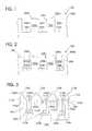
- FIGS. 1-6are cross-sectional views of gallium nitride semiconductor structures during intermediate fabrication steps, according to the present invention.
- a substrate 100also referred to as a “textured substrate”, is provided including a plurality of non-gallium nitride posts 100 a that define trenches 100 b therebetween.
- the non-gallium nitride posts 100 ainclude non-gallium nitride sidewalls 100 c and non-gallium nitride tops 100 d .
- the trenches 100 balso include non-gallium nitride floors 100 e.
- the substrate 100may be a monocrystalline substrate or a substrate including one or more monocrystalline layers thereon, from which the posts 100 a and trenches 100 b are defined.
- monocrystalline substrates and monocrystalline layersinclude, but are not limited to, monocrystalline silicon, silicon carbide and/or sapphire.
- the posts 100 a and trenches 100 bmay be defined using selective etching and/or selective epitaxial growth. Etching may be performed using standard dry or wet etching techniques, preferably using a mask, which then preferably is removed. The fabrication of a substrate including trenches and posts is well known to those having skill in the art and need not be described in detail herein.
- the substrate surface area that is available to contribute to defect formation during subsequent gallium nitride seed depositionmay be reduced and preferably minimized. Texturing also may reduce crack formation in the final gallium nitride semiconductor layer by providing stress relief during cooling. Stress may occur due to mismatches in the coefficients of thermal expansion between the substrate material and gallium nitride that is formed subsequently.
- the trenches 100 bpreferably are sufficiently deep so that undesirable growth of poor quality gallium nitride from the trench floor 100 e will not interfere with growth of high quality gallium nitride, as will be described below.
- the posts 100 apreferably are grown in the form of stripes that preferably are sufficiently narrow, for example less than or equal to one micron in width, so that small gallium nitride seed pyramids can be formed on the non-gallium nitride tops 100 d .
- the initial gallium nitride seed pyramids that form on the non-gallium nitride tops 100 dmay have defects, so that the reduced size gallium nitride seed pyramids can reduce the total amount of initial defective gallium nitride seed material.
- the total mechanical stress on the pyramids due to the differences in coefficients of thermal expansion between the substrate, any conformal buffer layers and the grown gallium nitridealso may be reduced, as well as the time to complete the pyramidal growth and initiate pendeoepitaxial growth as will be described below.
- the stripespreferably extend along the 1 ⁇ overscore (1) ⁇ 00 direction of a sapphire or silicon carbide substrate 100 and along the 110 direction of a silicon substrate 100 , to thereby expose the 11 ⁇ overscore (2) ⁇ 0 plane of the subsequently grown gallium nitride layer.
- the stripesshould expose the 11 ⁇ overscore (2) ⁇ 0 plane of sapphire and silicon carbide substrates.
- the wafer flatis the 0001 direction.
- etchingis performed parallel to the flat or the 0001 direction .
- the sidewalls 100 cmay not be orthogonal to the substrate 100 , but rather may be oblique thereto.
- the posts 100 a and trenches 100 bmay define elongated regions that are straight, V-shaped or have other shapes.
- the spaced apart posts 100 aalso may be referred to as “mesas”,“pedestals” or “columns”.
- the trenches 100 balso may be referred to as “wells”.
- an optional conformal buffer layer 102then may be formed on the substrate 100 including on the non-gallium nitride sidewalls 100 c , the non-gallium nitride tops 100 d and the non-gallium nitride floors 100 e .
- the buffer layermay comprise silicon carbide and/or aluminum nitride.
- the buffer layer 102may comprise high temperature aluminum nitride.
- the conformal buffer layer 102may comprise low temperature gallium nitride and/or aluminum nitride.
- Other buffer layersmay be used with these and other non-gallium nitride posts 100 a .
- the fabrication of a buffer layer on a substrateis well known to those having skill in the art and need not be described in detail herein.
- gallium nitrideis grown on the non-gallium nitride posts 100 a including on the non-gallium nitride tops 100 d . More specifically, a gallium nitride layer 110 is formed, wherein the gallium nitride layer includes gallium nitride pyramids 110 a on the non-gallium nitride tops 100 d . These pyramids 110 a also may be referred to as “seed form”. It will be understood that the seed forms need not be pyramidal in shape but rather may have flash tops. As also shown in FIG.
- second gallium nitride pyramids 110 balso may be formed simultaneously on the non-gallium nitride floors 100 e .
- a conformal region of gallium nitride 110 calso may be formed simultaneously on the sidewalls 100 c of the non-gallium nitride posts 100 a .
- Growth of the gallium nitride layer 110preferably is performed using metalorganic vapor phase epitaxy (MOVPE) of triethylgallium (TEG), for example at 13-39 ⁇ mol/min and NH 3 at 1500 sccm in combination with 3000 sccm H 2 diluent, at low temperature, preferably at about 1000° C. or less.
- MOVPEmetalorganic vapor phase epitaxy
- MOCVD growth of gallium nitridemay be found in the above-cited publications to Nam et al, Zheleva et al, Zheleva et al. and Linthicum et al. Other growth techniques also may be used.
- the present inventionpreferably produces pyramidal gallium nitride seed forms 110 a on the tops 110 d of the gallium nitride posts 110 a .
- Earlier studies that were conducted on selective area growth of gallium nitrideindicated that when gallium nitride pyramids are grown through mask windows, two regions of gallium nitride material result.
- One regionis a relatively high defect density gallium nitride area that converges at the apex of the pyramid. The other region is nearly defect-free and encapsulates the pyramid. See, for example, the publication by Nam et al.
- the pyramids 110 a on the tops 100 d of the non-gallium nitride posts 100 acan form these same two regions.
- the growth parameterscan be changed to enhance lateral growth of gallium nitride from the relatively defect free regions of the pyramids, and that can result in nearly defect-free gallium nitride epilayers, as will be described below.
- the pyramidspreferably are formed at relatively low temperature, preferably about 1000° C. or less using metalorganic vapor phase epitaxy, as was described above.
- the pyramidsmay be grown to have a width of about 2 ⁇ m and a height of about 2 ⁇ m on posts that are 1 ⁇ m wide.
- the interior portions 110 a ′ of the pyramids 110 a having a width of about 1 ⁇ m and a height of about 1 ⁇ mmay have a high defect density of about 10 8 cm ⁇ 2 or more, whereas the outer portions 110 a ′′ of the pyramids 110 a may be relatively low in defect, for example having defect density of about 10 5 cm ⁇ 2 or less.
- the conformal layer 110 c on the sidewalls 100 c of the posts 100 aalso may have a high defect density and the second pyramids 110 b on the floor 100 e also may have high defect density, for example greater than about 10 8 cm ⁇ 2 . It also will be understood that in FIG. 3 , masks need not be used prior to or during the growth of the gallium nitride layer 110 .
- gallium nitride 120then is preferentially laterally grown on the gallium nitride pyramids 110 a . Moreover, as shown in FIG. 4 , vertical growth also may occur. It will be understood that, as used herein the term “lateral” means a direction that is orthogonal to the sidewalls 100 c . As used herein, the term “vertical” denotes a direction parallel to the sidewalls 100 c.
- the crystal morphologymay change as the temperature increases.
- a pyramidal cross-sectionmay result as was shown in FIG. 3 .
- a rectangular cross-sectionmay result.
- gallium nitride 120is preferentially laterally grown from the outer portions 110 ′′ of the pyramids 110 a .
- growth from the low defect outer portions 110 a ′′ of the pyramids 110 amay have a lower density of line and planar defects. As shown in FIGS. 5 and 6 , growth preferably is allowed to continue until the gallium nitride layer 120 coalesces on the tops 100 d of the posts 100 a to form a continuous gallium nitride semiconductor layer 130 .
- the trenches 100 balso preferably are filled with gallium nitride during this growth.
- the III-V precursor ratioalso may be changed during metalorganic vapor phase epitaxy to increase lateral growth relative to the vertical growth. It will be understood that the III-V precursor ratio also may be changed during seed form growth, to produce pointed or flat top seed forms.
- lateral growthmay be enhanced by increasing the ammonia (Group V) flux and/or decreasing the gallium (Group III) flux, such that the overall V/III ratio increases.
- gallium nitride layer 120coalesces
- vertical growth of the continuous gallium nitride layer 130may be enhanced by decreasing the ammonia flux and/or by increasing the gallium flux, such that the overall V/III ratio decreases.
- gallium nitride shown in FIGS. 3-6need not use a mask Accordingly, a low defect continuous gallium nitride layer 130 may be fabricated without the need to form a mask on a gallium nitride layer. Process simplification thereby may occur. Moreover, the formation of the pyramids 110 a and the subsequent formation of the gallium nitride layer 120 may be performed in a single growth chamber, preferably by increasing the temperature and by leaving the other process parameters unchanged. Simplified processing therefore also may be provided.
- low defect density gallium nitride semiconductor layershaving defect density of about 10 5 cm ⁇ 2 or less may be grown on substrates including silicon, silicon carbide and/or other materials. Growth masks may be eliminated, and high quality gallium nitride may be formed in one growth run.
- the gallium nitride seed pyramids 110 acan confine the threading dislocations that stem from heteroepitaxial growth. Defect densities of less than about 10 5 cm ⁇ 2 may be obtained within the volume of the laterally grown gallium nitride material.
- the maximum volume of the low defect density gallium nitride layer 130need only be limited by the size of the substrate. Line defects that stem from the lattice misfit between the substrate and the epilayers preferably converge at the apex of the pyramid 110 a′ , thereby confining most of the defects to the interior portion 110 a′.
- gallium nitride structurescomprise a substrate 100 including a plurality of non-gallium nitride posts 100 a that define trenches 100 b therebetween.
- the non-gallium nitride posts 100 ainclude non-gallium nitride sidewalls 100 c non-gallium nitride tops 100 d .
- the trenchesinclude non-gallium nitride floors 100 e .
- a gallium nitride layer 100is included on the non-gallium nitride posts 100 a including on the non-gallium nitride tops 100 d .
- the gallium nitride layer 110preferably comprises gallium nitride pyramids 100 a on the non-gallium nitride tops 100 d .
- Gallium nitride regions 120may be provided on the gallium nitride pyramids 110 a .
- Second gallium nitride pyramids 110 balso may be provided on the non-gallium nitride floors 100 e .
- a conformal gallium nitride layer 100 calso may be provided on the sidewalls 100 c between the gallium nitride pyramids 110 a and the second gallium nitride pyramids 100 b .
- the gallium nitride regions 120preferably form a continuous gallium nitride layer 130 .
- the gallium nitride layer 110also preferably fills the trenches.
- a conformal buffer layer 102also may be provided on the substrate, wherein the gallium nitride layer 110 is on the conform
Landscapes
- Engineering & Computer Science (AREA)
- Physics & Mathematics (AREA)
- Condensed Matter Physics & Semiconductors (AREA)
- General Physics & Mathematics (AREA)
- Manufacturing & Machinery (AREA)
- Computer Hardware Design (AREA)
- Microelectronics & Electronic Packaging (AREA)
- Power Engineering (AREA)
- Chemical & Material Sciences (AREA)
- Materials Engineering (AREA)
- Crystallography & Structural Chemistry (AREA)
Abstract
Description
This application is a continuation application of, and claims priority from, U.S. patent application Ser. No. 09/501,051, filed Feb. 9, 2000, now U.S. Pat. No. 6,403,451, the entire disclosure of which is incorporated herein by reference.
This invention was made with Government support under Office of Naval Research Contract Nos. N00014-96-1-0765, N00014-98-1-0384, and N00014-98-1-0654. The Government may have certain rights to this invention.
This invention relates to microelectronic devices and fabrication methods, and more particularly to gallium nitride semiconductor devices and fabrication methods therefor.
Gallium nitride is being widely investigated for microelectronic devices including but not limited to transistors, field emitters and optoelectronic devices. It will be understood that, as used herein, gallium nitride also includes alloys of gallium nitride such as aluminum gallium nitride, indium gallium nitride and aluminum indium gallium nitride.
A major problem in fabricating gallium nitride-based microelectronic devices is the fabrication of gallium nitride semiconductor layers having low defect densities. It is known that one contributor to defect density is the substrate on which the gallium nitride layer is grown. Accordingly, although gallium nitride layers have been grown on sapphire substrates, it is known to reduce defect density by growing gallium nitride layers on aluminum nitride buffer layers which are themselves formed on silicon carbide substrates. Notwithstanding these advances, continued reduction in defect density is desirable.
It also is known to produce low defect density gallium nitride layers by forming a mask on a layer of gallium nitride, the mask including at least one opening therein that exposes the underlying layer of gallium nitride, and laterally growing the underlying layer of gallium nitride through the at least one opening and onto the mask. This technique often is referred to as “Epitaxial Lateral Overgrowth” (ELO). The layer of gallium nitride may be laterally grown until the gallium nitride coalesces on the mask to form a single layer on the mask. In order to form a continuous layer of gallium nitride with relatively low defect density, a second mask may be formed on the laterally overgrown gallium nitride layer, that includes at least one opening that is offset from the opening in the underlying mask. ELO then again is performed through the openings in the second mask to thereby overgrow a second low defect density continuous gallium nitride layer. Microelectronic devices then may be formed in this second overgrown layer. ELO of gallium nitride is described, for example, in the publications entitledLateral Epitaxy of Low Defect Density GaN Layers Via Organometallic Vapor Phase Epitaxyto Nam et al., Appl. Phys. Lett. Vol. 71, No. 18, Nov. 3, 1997, pp. 2638-2640; andDislocation Density Reduction Via Lateral Epitaxy in Selectively Grown GaN Structuresto Zheleva et al, Appl. Phys. Lett., Vol. 71, No. 17, Oct. 27, 1997, pp. 2472-2474, the disclosures of which are hereby incorporated herein by reference.
It also is known to produce a layer of gallium nitride with low defect density by forming at least one trench or post in an underlying layer of gallium nitride to define at least one sidewall therein. A layer of gallium nitride is then laterally grown from the at least one sidewall. Lateral growth preferably takes place until the laterally grown layers coalesce within the trenches. Lateral growth also preferably continues until the gallium nitride layer that is grown from the sidewalls laterally overgrows onto the tops of the posts. In order to facilitate lateral growth and produce nucleation of gallium nitride and growth in the vertical direction, the top of the posts and/or the trench floors may be masked. Lateral growth from the sidewalls of trenches and/or posts also is referred to as “pendeoepitaxy” and is described, for example, in publications entitledPendeo-Epitaxy: A New Approach for Lateral Growth of Gallium Nitride Filmsby Zheleva et al., Journal of Electronic Materials, Vol. 28, No. 4, February 1999, pp. L5-L8; andPendeoepitaxy of Gallium Nitride Thin Filmsby Linthicum et al., Applied Physics Letters, Vol. 75, No. 2, July 1999, pp. 196-198, the disclosures of which are hereby incorporated herein by reference.
Unfortunately, both ELO and pendeoepitaxy may use one or more masks to mask portions of an underlying gallium nitride layer during ELO and/or pendeoepitaxy. These masks may complicate the fabrication process. Moreover, multiple growth steps of gallium nitride may be needed with mask formation therebetween. These multiple growth steps also may complicate the fabrication processes, because the structures may need to be removed from the gallium nitride growth chamber in order to form the mask or masks. Accordingly, notwithstanding the recent advances in ELO and pendeoepitaxy, there continues to be a need for methods of fabricating gallium nitride semiconductor layers that do not need masking layers and/or need not interrupt the gallium nitride growth process.
The present invention provides a substrate including non-gallium nitride posts that define trenches therebetween, wherein the non-gallium nitride posts include non-gallium nitride sidewalls and non-gallium nitride tops, and the trenches include non-gallium floors. These substrates also may be referred to herein as “textured” substrates. Then, gallium nitride is grown on the non-gallium nitride posts, including on the non-gallium nitride tops. Preferably, gallium nitride pyramids are grown on the non-gallium nitride tops and gallium nitride then is grown on the gallium nitride pyramids. The gallium nitride pyramids preferably are grown at a first temperature and the gallium nitride preferably is grown on the pyramids at a second temperature that is higher than the first temperature. The first temperature preferably is about 1000° C. or less and the second temperature preferably is about 1100° C. or more. However, other than temperature, the same processing conditions preferably are used for both growth steps. The grown gallium nitride on the pyramids preferably coalesces to form a continuous gallium nitride layer.
Accordingly, gallium nitride may be grown on a textured substrate, without the need to provide masks during the gallium nitride growth process. Moreover, the gallium nitride growth may be performed using the same processing conditions other than temperatures changes. Accordingly, uninterrupted gallium nitride growth may be performed. Simplified processing conditions therefore may be employed to grow a gallium nitride layer having low defect densities, for example defect densities of less than about 105cm−2.
During growth of the gallium nitride pyramids on the non-gallium nitride tops, gallium nitride pyramids also may be simultaneously grown on the non-gallium nitride floors. Moreover, a conformal gallium nitride layer also may be formed simultaneously on the sidewalls, between the gallium nitride pyramids on the non-gallium nitride tops and on the non-gallium nitride floors. Upon growing the gallium nitride on the pyramids, the trenches also may be simultaneously filled with gallium nitride. A conformal buffer layer may be formed on the substrate including on the non-gallium nitride sidewalls, the non-gallium nitride tops and the non-gallium nitride floors, prior to growing the gallium nitride pyramids. For example, a conformal layer of aluminum nitride may be used.
Gallium nitride semiconductor structures therefore may be fabricated, according to the present invention, by providing a textured substrate, including a plurality of non-gallium nitride posts that define trenches therebetween, wherein the non-gallium nitride posts include non-gallium nitride sidewalls and non-gallium nitride tops, and the trenches include non-gallium nitride floors. The substrate preferably is free of masking materials on the non-gallium nitride floors and on the non-gallium nitride tops. Gallium nitride then is grown at a first temperature and the growth of gallium nitride then is continued at a second temperature that is higher than the first temperature. Growth at the second temperature preferably continues until the gallium nitride forms a continuous gallium nitride layer on the substrate.
Gallium nitride semiconductor structures according to the present invention preferably comprise a textured substrate including a plurality of non-gallium nitride posts that define trenches therebetween, the non-gallium nitride posts including non-gallium nitride sidewalls and non-gallium nitride tops, and the trenches including non-gallium nitride floors. A gallium nitride layer is provided on the non-gallium nitride posts including on the non-gallium nitride tops. The gallium nitride semiconductor structure preferably is free of a masking layer on the non-gallium nitride tops and on the non-gallium nitride floors. The gallium nitride layer preferably comprises gallium nitride pyramids on the non-gallium nitride tops. The gallium nitride layer may also include gallium nitride regions on the gallium nitride pyramids. Second gallium nitride pyramids on the non-gallium nitride floors also may be provided. A conformal gallium nitride layer on the sidewalls, between the gallium nitride pyramids and the second gallium nitride pyramids also may be provided. The gallium nitride regions preferably form a continuous gallium nitride layer and the gallium nitride layer also preferably fills the trenches. A conformal buffer layer also may be provided on the substrate wherein the gallium nitride layer is on the conformal buffer layer opposite the substrate.
The present invention most preferably may be used to provide methods of fabricating gallium nitride semiconductor structures that need not include masking or interruptions during gallium nitride epitaxial growth. Accordingly, simplified processes for fabricating gallium nitride semiconductor structures may be provided, to thereby fulfill a need in the fledgling gallium nitride semiconductor industry. However, it also will be understood that the present invention may be used to fabricate non-gallium nitride semiconductor structures wherein a textured substrate of a first material is provided and a second semiconductor material is grown on the posts including on the tops that comprise the first material. Also, semiconductor structures may be provided including a textured substrate that comprises a first material and a layer of second semiconductor material on the posts that comprise the first material.
The present invention now will be described more fully hereinafter with reference to the accompanying drawings, in which preferred embodiments of the invention are shown. This invention may, however, be embodied in many different forms and should not be construed as limited to the embodiments set forth herein; rather, these embodiments are provided so that this disclosure will be thorough and complete, and will fully convey the scope of the invention to those skilled in the art. In the drawings, the thickness of layers and regions are exaggerated for clarity. Like numbers refer to like elements throughout. It will be understood that when an element such as a layer, region or substrate is referred to as being “on” another element, it can be directly on the other element or intervening elements may also be present. Moreover, each embodiment described and illustrated herein includes its complementary conductivity type embodiment as well.
Referring now toFIGS. 1-6 , methods of fabricating gallium nitride semiconductor structures according to embodiments of the present invention now will described. As shown inFIG. 1 , asubstrate 100, also referred to as a “textured substrate”, is provided including a plurality of non-gallium nitride posts100athat definetrenches 100btherebetween. The non-gallium nitride posts100aincludenon-gallium nitride sidewalls 100cand non-gallium nitride tops100d. Thetrenches 100balso includenon-gallium nitride floors 100e.
It will be understood by those having skill in the art that thesubstrate 100 may be a monocrystalline substrate or a substrate including one or more monocrystalline layers thereon, from which theposts 100aandtrenches 100bare defined. Examples of monocrystalline substrates and monocrystalline layers include, but are not limited to, monocrystalline silicon, silicon carbide and/or sapphire. It also will be understood that theposts 100aandtrenches 100bmay be defined using selective etching and/or selective epitaxial growth. Etching may be performed using standard dry or wet etching techniques, preferably using a mask, which then preferably is removed. The fabrication of a substrate including trenches and posts is well known to those having skill in the art and need not be described in detail herein.
As will be shown below, by texturing thesubstrate 100, the substrate surface area that is available to contribute to defect formation during subsequent gallium nitride seed deposition may be reduced and preferably minimized. Texturing also may reduce crack formation in the final gallium nitride semiconductor layer by providing stress relief during cooling. Stress may occur due to mismatches in the coefficients of thermal expansion between the substrate material and gallium nitride that is formed subsequently.
It also will be understood that thetrenches 100bpreferably are sufficiently deep so that undesirable growth of poor quality gallium nitride from thetrench floor 100ewill not interfere with growth of high quality gallium nitride, as will be described below. Moreover, theposts 100apreferably are grown in the form of stripes that preferably are sufficiently narrow, for example less than or equal to one micron in width, so that small gallium nitride seed pyramids can be formed on the non-gallium nitride tops100d. As will be described below, the initial gallium nitride seed pyramids that form on the non-gallium nitride tops100dmay have defects, so that the reduced size gallium nitride seed pyramids can reduce the total amount of initial defective gallium nitride seed material. The total mechanical stress on the pyramids due to the differences in coefficients of thermal expansion between the substrate, any conformal buffer layers and the grown gallium nitride also may be reduced, as well as the time to complete the pyramidal growth and initiate pendeoepitaxial growth as will be described below.
When theposts 100aare in the form of stripes, the stripes preferably extend along the 1{overscore (1)}00 direction of a sapphire orsilicon carbide substrate 100 and along the 110 direction of asilicon substrate 100, to thereby expose the 11{overscore (2)}0 plane of the subsequently grown gallium nitride layer. In general, the stripes should expose the 11{overscore (2)}0 plane of sapphire and silicon carbide substrates. For example, if A-plane sapphire is used, as opposed to C-plane sapphire which is more common, then the wafer flat is the 0001 direction. In order to expose the 11{overscore (2)}0 plane, etching is performed parallel to the flat or the 0001 direction . However, it also will be understood that thesidewalls 100cmay not be orthogonal to thesubstrate 100, but rather may be oblique thereto. Finally, it also will be understood that, although thesidewalls 100care shown in cross-section inFIG. 1 , theposts 100aandtrenches 100bmay define elongated regions that are straight, V-shaped or have other shapes. The spaced apart posts100aalso may be referred to as “mesas”,“pedestals” or “columns”. Thetrenches 100balso may be referred to as “wells”.
Referring now toFIG. 2 , an optionalconformal buffer layer 102 then may be formed on thesubstrate 100 including on thenon-gallium nitride sidewalls 100c, the non-gallium nitride tops100dand thenon-gallium nitride floors 100e. When the non-gallium nitride posts100acomprise silicon, the buffer layer may comprise silicon carbide and/or aluminum nitride. When the non-gallium nitride posts100acomprise silicon carbide, thebuffer layer 102 may comprise high temperature aluminum nitride. Finally, when the non-gallium nitride posts100acomprise sapphire, theconformal buffer layer 102 may comprise low temperature gallium nitride and/or aluminum nitride. Other buffer layers may be used with these and other non-gallium nitride posts100a. The fabrication of a buffer layer on a substrate is well known to those having skill in the art and need not be described in detail herein.
Referring now toFIG. 3 , gallium nitride is grown on the non-gallium nitride posts100aincluding on the non-gallium nitride tops100d. More specifically, agallium nitride layer 110 is formed, wherein the gallium nitride layer includesgallium nitride pyramids 110aon the non-gallium nitride tops100d. Thesepyramids 110aalso may be referred to as “seed form”. It will be understood that the seed forms need not be pyramidal in shape but rather may have flash tops. As also shown inFIG. 3 , secondgallium nitride pyramids 110balso may be formed simultaneously on thenon-gallium nitride floors 100e. Finally, a conformal region ofgallium nitride 110calso may be formed simultaneously on thesidewalls 100cof the non-gallium nitride posts100a. Growth of thegallium nitride layer 110 preferably is performed using metalorganic vapor phase epitaxy (MOVPE) of triethylgallium (TEG), for example at 13-39 μmol/min and NH3at 1500 sccm in combination with 3000 sccm H2diluent, at low temperature, preferably at about 1000° C. or less. Additional details of MOCVD growth of gallium nitride may be found in the above-cited publications to Nam et al, Zheleva et al, Zheleva et al. and Linthicum et al. Other growth techniques also may be used.
Details of the growth ofgallium nitride layer 110 now will be described. In particular, as shown inFIG. 3 , the present invention preferably produces pyramidal gallium nitride seed forms110aon the tops110dof thegallium nitride posts 110a. Earlier studies that were conducted on selective area growth of gallium nitride indicated that when gallium nitride pyramids are grown through mask windows, two regions of gallium nitride material result. One region is a relatively high defect density gallium nitride area that converges at the apex of the pyramid. The other region is nearly defect-free and encapsulates the pyramid. See, for example, the publication by Nam et al. entitledLateral Epitaxial Overgrowth of GaN Films on SiO2Areas via Metalorganic Vapor Phase Epitaxy, Journal of Electronic Materials, Vol. 27, No. 4, 1998, pp. 233-237, the disclosure of which is hereby incorporated herein by reference.
According to the invention, thepyramids 110aon the tops100dof the non-gallium nitride posts100acan form these same two regions. Once the nearly defect-free region is formed, the growth parameters can be changed to enhance lateral growth of gallium nitride from the relatively defect free regions of the pyramids, and that can result in nearly defect-free gallium nitride epilayers, as will be described below.
In particular, the pyramids preferably are formed at relatively low temperature, preferably about 1000° C. or less using metalorganic vapor phase epitaxy, as was described above. The pyramids may be grown to have a width of about 2 μm and a height of about 2 μm on posts that are 1 μm wide. In this case, theinterior portions 110a′ of thepyramids 110ahaving a width of about 1 μm and a height of about 1 μm, may have a high defect density of about 108cm−2or more, whereas theouter portions 110a″ of thepyramids 110amay be relatively low in defect, for example having defect density of about 105cm−2or less. Theconformal layer 110con thesidewalls 100cof theposts 100aalso may have a high defect density and thesecond pyramids 110bon thefloor 100ealso may have high defect density, for example greater than about 108cm−2. It also will be understood that inFIG. 3 , masks need not be used prior to or during the growth of thegallium nitride layer 110.
Referring now toFIG. 4 ,gallium nitride 120 then is preferentially laterally grown on thegallium nitride pyramids 110a. Moreover, as shown inFIG. 4 , vertical growth also may occur. It will be understood that, as used herein the term “lateral” means a direction that is orthogonal to thesidewalls 100c. As used herein, the term “vertical” denotes a direction parallel to thesidewalls 100c.
For stripes oriented along the 1{overscore (1)}00 direction, the crystal morphology may change as the temperature increases. Thus, at lower temperatures, for example at about 1000° C. or less, a pyramidal cross-section may result as was shown in FIG.3. At higher temperatures, for example at about 1100° C. or more, a rectangular cross-section may result. Thus, by increasing the temperature, for example to about 1100° C. or more, and preferably without changing any other growth parameters,gallium nitride 120 is preferentially laterally grown from theouter portions 110″ of thepyramids 110a. Similar to ELO or pendeoepitaxy of gallium nitride, growth from the low defectouter portions 110a″ of thepyramids 110amay have a lower density of line and planar defects. As shown inFIGS. 5 and 6 , growth preferably is allowed to continue until thegallium nitride layer 120 coalesces on the tops100dof theposts 100ato form a continuous galliumnitride semiconductor layer 130. Thetrenches 100balso preferably are filled with gallium nitride during this growth.
It will be understood that the III-V precursor ratio also may be changed during metalorganic vapor phase epitaxy to increase lateral growth relative to the vertical growth. It will be understood that the III-V precursor ratio also may be changed during seed form growth, to produce pointed or flat top seed forms. In particular, lateral growth may be enhanced by increasing the ammonia (Group V) flux and/or decreasing the gallium (Group III) flux, such that the overall V/III ratio increases. Once thegallium nitride layer 120 coalesces, vertical growth of the continuousgallium nitride layer 130 may be enhanced by decreasing the ammonia flux and/or by increasing the gallium flux, such that the overall V/III ratio decreases.
The growth of gallium nitride shown inFIGS. 3-6 need not use a mask Accordingly, a low defect continuousgallium nitride layer 130 may be fabricated without the need to form a mask on a gallium nitride layer. Process simplification thereby may occur. Moreover, the formation of thepyramids 110aand the subsequent formation of thegallium nitride layer 120 may be performed in a single growth chamber, preferably by increasing the temperature and by leaving the other process parameters unchanged. Simplified processing therefore also may be provided.
Accordingly, low defect density gallium nitride semiconductor layers, having defect density of about 105cm−2or less may be grown on substrates including silicon, silicon carbide and/or other materials. Growth masks may be eliminated, and high quality gallium nitride may be formed in one growth run. The galliumnitride seed pyramids 110acan confine the threading dislocations that stem from heteroepitaxial growth. Defect densities of less than about 105cm−2may be obtained within the volume of the laterally grown gallium nitride material. The maximum volume of the low defect densitygallium nitride layer 130 need only be limited by the size of the substrate. Line defects that stem from the lattice misfit between the substrate and the epilayers preferably converge at the apex of thepyramid 110a′, thereby confining most of the defects to theinterior portion 110a′.
Referring again toFIG. 6 , gallium nitride structures according to the present invention comprise asubstrate 100 including a plurality of non-gallium nitride posts100athat definetrenches 100btherebetween. The non-gallium nitride posts100aincludenon-gallium nitride sidewalls 100cnon-gallium nitride tops100d. The trenches includenon-gallium nitride floors 100e. Agallium nitride layer 100 is included on the non-gallium nitride posts100aincluding on the non-gallium nitride tops100d. Thegallium nitride layer 110 preferably comprisesgallium nitride pyramids 100aon the non-gallium nitride tops100d.Gallium nitride regions 120 may be provided on thegallium nitride pyramids 110a. Secondgallium nitride pyramids 110balso may be provided on thenon-gallium nitride floors 100e. A conformalgallium nitride layer 100calso may be provided on thesidewalls 100cbetween thegallium nitride pyramids 110aand the secondgallium nitride pyramids 100b. Thegallium nitride regions 120 preferably form a continuousgallium nitride layer 130. Thegallium nitride layer 110 also preferably fills the trenches. Aconformal buffer layer 102 also may be provided on the substrate, wherein thegallium nitride layer 110 is on theconformal buffer layer 102 opposite thesubstrate 100.
In the drawings and specification, there have been disclosed typical preferred embodiments of the invention and, although specific terms are employed, they are used in a generic and descriptive sense only and not for purposes of limitation, the scope of the invention being set forth in the following claims.
Claims (41)
1. A method of fabricating gallium nitride semiconductor structures comprising the steps of:
providing a substrate including a plurality of non-gallium nitride posts that define trenches therebetween, the non-gallium nitride posts including non-gallium nitride sidewalls and non-gallium nitride tops, and the trenches including non-gallium nitride floors; and
growing gallium nitride on the non-gallium nitride posts, including on the non-gallium nitride tops.
2. A method according toclaim 1 wherein the growing step comprises the steps of:
first growing the gallium nitride at a first temperature; and
then growing the gallium nitride at a second temperature that is higher then the first temperature.
3. A method according toclaim 1 wherein the following step is performed between the steps of providing and growing:
forming a conformal buffer layer on the substrate including on the non-gallium nitride sidewalls, the non-gallium nitride tops and the non-gallium nitride floors.
4. A method according toclaim 1 wherein the providing step comprises the steps of:
providing a non-gallium nitride substrate; and
etching the non-gallium nitride substrate to define the plurality of non-gallium nitride posts and the trenches therebetween.
5. A method according toclaim 2 wherein the first temperature is at most about 1000° C. and wherein the second temperature is at least about 1100° C.
6. A method according toclaim 1 wherein the growing step comprises the step of masklessly growing gallium nitride on the non-gallium nitride posts, including on the non-gallium nitride taps.
7. A method according toclaim 1 wherein the non-gallium nitride sidewalls expose a 11{overscore (2)}0 plane of the non-gallium nitride posts.
8. A method of fabricating gallium nitride semiconductor structures comprising the steps of:
providing a substrate including a plurality of non-gallium nitride posts that define trenches therebetween, the non-gallium nitride posts including non-gallium nitride sidewall, and non-gallium nitride tops, and the trenches including non-gallium nitride floors;
growing gallium nitride on the substrate at a first temperature; and then
continuing growing gallium nitride on the substrate at a second temperature that is higher than the first temperature.
9. A method according toclaim 8 wherein the first temperature is at most about 1000° C. and wherein the second temperature is at least about 1100° C.
10. A method according toclaim 8 wherein the step of continuing growing comprises the step of continuing growing gallium nitride on the substrate at the second temperature until the gallium nitride forms a continuous gallium nitride layer on the substrate.
11. A method according toclaim 8 wherein the step of growing gallium nitride and the step of continuing growing gallium nitride are performed at same processing conditions other than temperature.
12. A method according toclaim 8 wherein the following step is performed between the steps of providing and growing:
forming a conformal buffer layer on the substrate including on the non-gallium nitride sidewalls, the non-gallium nitride tops and the non-gallium nitride floors.
13. A method according toclaim 8 wherein the providing step comprises the steps of:
providing a non-gallium nitride substrate; and
etching the non-gallium nitride substrate to define the plurality of non-gallium nitride posts and the trenches therebetween.
14. A method according toclaim 8 wherein the growing and continuing growing steps comprise the steps of masklessly growing gallium nitride and masklessly continuing growing gallium nitride.
15. A method according toclaim 1 wherein the non-gallium nitride sidewalls expose a 11{overscore (2)}0 plane of the non-gallium nitride posts.
16. A method according toclaim 1 , comprising growing gallium nitride on the non-gallium nitride posts in a non-vertical direction and toward the trenches.
17. A method according toclaim 1 , comprising growing gallium nitride on the non-gallium nitride posts in a non-vertical direction until a gallium nitride layer extends over the trenches.
18. A method according toclaim 17 , comprising growing gallium nitride on the non-gallium nitride posts in a non-vertical direction until gallium nitride growing on adjacent non-gallium nitride posts coalesces to form a continuous gallium nitride layer that extends over the trench defined by the adjacent non-gallium nitride posts.
19. A method according toclaim 18 , further comprising vertically growing the continuous gallium nitride layer.
20. A method according toclaim 1 , comprising growing gallium nitride on the non-gallium nitride tops of the non-gallium nitride posts in a non-vertical direction.
21. A method according toclaim 1 , comprising growing gallium nitride on the non-gallium nitride sidewalls of the non-gallium nitride posts in a non-vertical direction.
22. A method according toclaim 1 , further comprising growing gallium nitride on the non-gallium nitride floors.
23. A method according toclaim 1 , wherein the step of providing the substrate includes etching the substrate to form the plurality of non-gallium nitride posts that define trenches therebetween.
24. A method according toclaim 1 , wherein the non-gallium nitride posts are stripes.
25. A method according toclaim 1 , wherein the non-gallium nitride stripes extend in a 1-100 direction of the substrate.
26. A method according toclaim 1 , wherein the non-gallium nitride posts stripes extend in a 110 direction of the substrate.
27. A method according toclaim 1 , wherein the non-gallium nitride sidewalls are orthogonal to the substrate.
28. A method according toclaim 1 , wherein the non-gallium nitride sidewalls are oblique to the substrate.
29. A method according toclaim 1 , further comprising growing a gallium nitride seed form on the non-gallium nitride tops of the gallium nitride posts.
30. A method according toclaim 29 , comprising growing the gallium nitride seed form in a non-vertical direction.
31. A method according toclaim 1 , wherein the gallium nitride grown in a direction parallel to the non-gallium nitride tops has a defect density off less than or equal to about 105cm−2.
32. A method according toclaim 1 , wherein the substrate is a silicon substrate.
33. A method according toclaim 1 , wherein the substrate is a sapphire substrate.
34. A method according toclaim 1 , wherein the substrate is a silicon carbide substrate.
35. A method according toclaim 1 , wherein the substrate and the non-gallium nitride posts comprise a first material.
36. A method according toclaim 1 , further comprising growing a conformal buffer layer on the non-gallium nitride tops of the non-gallium nitride posts prior to growing gallium nitride on the non-gallium nitride posts in a non-vertical direction.
37. A method according toclaim 36 , wherein the conformal buffer layer is gallium nitride.
38. A method according toclaim 36 , wherein the conformal buffer layer is aluminum nitride.
39. A method according toclaim 1 , comprising growing gallium nitride on the non-gallium nitride posts in a non-vertical direction.
40. A method according toclaim 39 , comprising growing gallium nitride on respective non-gallium nitride posts in a direction toward trenches formed adjacent to the respective non-gallium nitride posts.
41. A method according toclaim 1 , comprising laterally growing gallium nitride on non-gallium nitride posts.
Priority Applications (2)
| Application Number | Priority Date | Filing Date | Title |
|---|---|---|---|
| US10/115,354US6864160B2 (en) | 2000-02-09 | 2002-04-03 | Methods of fabricating gallium nitride semiconductor layers on substrates including non-gallium nitride posts |
| US11/074,485US7095062B2 (en) | 2000-02-09 | 2005-03-08 | Methods of fabricating gallium nitride semiconductor layers on substrates including non-gallium nitride posts, and gallium nitride semiconductor structures fabricated thereby |
Applications Claiming Priority (2)
| Application Number | Priority Date | Filing Date | Title |
|---|---|---|---|
| US09/501,051US6403451B1 (en) | 2000-02-09 | 2000-02-09 | Methods of fabricating gallium nitride semiconductor layers on substrates including non-gallium nitride posts |
| US10/115,354US6864160B2 (en) | 2000-02-09 | 2002-04-03 | Methods of fabricating gallium nitride semiconductor layers on substrates including non-gallium nitride posts |
Related Parent Applications (1)
| Application Number | Title | Priority Date | Filing Date |
|---|---|---|---|
| US09/501,051ContinuationUS6403451B1 (en) | 2000-02-09 | 2000-02-09 | Methods of fabricating gallium nitride semiconductor layers on substrates including non-gallium nitride posts |
Related Child Applications (1)
| Application Number | Title | Priority Date | Filing Date |
|---|---|---|---|
| US11/074,485ContinuationUS7095062B2 (en) | 2000-02-09 | 2005-03-08 | Methods of fabricating gallium nitride semiconductor layers on substrates including non-gallium nitride posts, and gallium nitride semiconductor structures fabricated thereby |
Publications (2)
| Publication Number | Publication Date |
|---|---|
| US20020110997A1 US20020110997A1 (en) | 2002-08-15 |
| US6864160B2true US6864160B2 (en) | 2005-03-08 |
Family
ID=23991950
Family Applications (4)
| Application Number | Title | Priority Date | Filing Date |
|---|---|---|---|
| US09/501,051Expired - LifetimeUS6403451B1 (en) | 2000-02-09 | 2000-02-09 | Methods of fabricating gallium nitride semiconductor layers on substrates including non-gallium nitride posts |
| US09/973,383Expired - LifetimeUS6621148B2 (en) | 2000-02-09 | 2001-10-09 | Methods of fabricating gallium nitride semiconductor layers on substrates including non-gallium nitride posts, and gallium nitride semiconductor structures fabricated thereby |
| US10/115,354Expired - LifetimeUS6864160B2 (en) | 2000-02-09 | 2002-04-03 | Methods of fabricating gallium nitride semiconductor layers on substrates including non-gallium nitride posts |
| US11/074,485Expired - LifetimeUS7095062B2 (en) | 2000-02-09 | 2005-03-08 | Methods of fabricating gallium nitride semiconductor layers on substrates including non-gallium nitride posts, and gallium nitride semiconductor structures fabricated thereby |
Family Applications Before (2)
| Application Number | Title | Priority Date | Filing Date |
|---|---|---|---|
| US09/501,051Expired - LifetimeUS6403451B1 (en) | 2000-02-09 | 2000-02-09 | Methods of fabricating gallium nitride semiconductor layers on substrates including non-gallium nitride posts |
| US09/973,383Expired - LifetimeUS6621148B2 (en) | 2000-02-09 | 2001-10-09 | Methods of fabricating gallium nitride semiconductor layers on substrates including non-gallium nitride posts, and gallium nitride semiconductor structures fabricated thereby |
Family Applications After (1)
| Application Number | Title | Priority Date | Filing Date |
|---|---|---|---|
| US11/074,485Expired - LifetimeUS7095062B2 (en) | 2000-02-09 | 2005-03-08 | Methods of fabricating gallium nitride semiconductor layers on substrates including non-gallium nitride posts, and gallium nitride semiconductor structures fabricated thereby |
Country Status (1)
| Country | Link |
|---|---|
| US (4) | US6403451B1 (en) |
Cited By (12)
| Publication number | Priority date | Publication date | Assignee | Title |
|---|---|---|---|---|
| US20050009304A1 (en)* | 1998-06-10 | 2005-01-13 | Tsvetanka Zheleva | Methods of fabricating gallium nitride semiconductor layers by lateral growth into trenches |
| US20050014303A1 (en)* | 2003-06-18 | 2005-01-20 | United Epitaxy Company, Ltd. | Method for manufacturing semiconductor light-emitting device |
| US20050250234A1 (en)* | 2004-05-10 | 2005-11-10 | Sharp Kabushiki Kaisha | Semiconductor device and method for fabrication thereof |
| US20050263778A1 (en)* | 2001-02-27 | 2005-12-01 | Sanyo Electric Co., Ltd. | Nitride-based semiconductor element and method of forming nitride-based semiconductor |
| US20070000433A1 (en)* | 2005-06-15 | 2007-01-04 | Mike Briere | III-nitride semiconductor device fabrication |
| US20070190678A1 (en)* | 2003-12-31 | 2007-08-16 | Johngeon Shin | Nitride semiconductor thin film having fewer defects and method of growing the same |
| US20080080578A1 (en)* | 2004-01-05 | 2008-04-03 | Sharp Kabushiki Kaisha | Nitride semiconductor laser device and method for fabrication thereof |
| US20080102598A1 (en)* | 2006-10-30 | 2008-05-01 | Thomas Herman | III-Nitride wafer fabrication |
| US20080166852A1 (en)* | 2004-06-10 | 2008-07-10 | Sharp Kabushiki Kaisha | Semiconductor element, semiconductor device, and method for fabrication thereof |
| US20100308437A1 (en)* | 2008-01-29 | 2010-12-09 | Koji Okuno | Method for producing group iii nitride-based compound semiconductor, wafer including group iii nitride-based compound semiconductor, and group iii nitrided-based compound semiconductor device |
| US20110147703A1 (en)* | 2009-12-17 | 2011-06-23 | Lehigh University | ABBREVIATED EPITAXIAL GROWTH MODE (AGM) METHOD FOR REDUCING COST AND IMPROVING QUALITY OF LEDs AND LASERS |
| US20120086017A1 (en)* | 2009-06-15 | 2012-04-12 | Korea Electronics Technology Institute | Heterogeneous substrate, nitride-based semiconductor device using same, and manufacturing method thereof |
Families Citing this family (117)
| Publication number | Priority date | Publication date | Assignee | Title |
|---|---|---|---|---|
| US6177688B1 (en) | 1998-11-24 | 2001-01-23 | North Carolina State University | Pendeoepitaxial gallium nitride semiconductor layers on silcon carbide substrates |
| WO2000055893A1 (en)* | 1999-03-17 | 2000-09-21 | Mitsubishi Cable Industries, Ltd. | Semiconductor base and its manufacturing method, and semiconductor crystal manufacturing method |
| JP4432180B2 (en)* | 1999-12-24 | 2010-03-17 | 豊田合成株式会社 | Group III nitride compound semiconductor manufacturing method, group III nitride compound semiconductor device, and group III nitride compound semiconductor |
| US6403451B1 (en)* | 2000-02-09 | 2002-06-11 | Noerh Carolina State University | Methods of fabricating gallium nitride semiconductor layers on substrates including non-gallium nitride posts |
| JP2001267242A (en)* | 2000-03-14 | 2001-09-28 | Toyoda Gosei Co Ltd | Group III nitride compound semiconductor and method of manufacturing the same |
| US6836498B2 (en)* | 2000-06-05 | 2004-12-28 | Sony Corporation | Semiconductor laser, semiconductor device and nitride series III-V group compound substrate, as well as manufacturing method thereof |
| JP5095064B2 (en)* | 2000-08-04 | 2012-12-12 | ザ リージェンツ オブ ザ ユニバーシティ オブ カリフォルニア | Semiconductor film having nitride layer deposited on silicon substrate and method for manufacturing the same |
| JP3863720B2 (en)* | 2000-10-04 | 2006-12-27 | 三洋電機株式会社 | Nitride semiconductor device and method for forming nitride semiconductor |
| US6649287B2 (en) | 2000-12-14 | 2003-11-18 | Nitronex Corporation | Gallium nitride materials and methods |
| WO2002064864A1 (en)* | 2001-02-14 | 2002-08-22 | Toyoda Gosei Co., Ltd. | Production method for semiconductor crystal and semiconductor luminous element |
| US6956250B2 (en)* | 2001-02-23 | 2005-10-18 | Nitronex Corporation | Gallium nitride materials including thermally conductive regions |
| US6939730B2 (en)* | 2001-04-24 | 2005-09-06 | Sony Corporation | Nitride semiconductor, semiconductor device, and method of manufacturing the same |
| GB0128743D0 (en)* | 2001-11-30 | 2002-01-23 | Epiic Ltd | Method of producing integrated semiconductor components on a semiconductor substrate |
| US20030132433A1 (en)* | 2002-01-15 | 2003-07-17 | Piner Edwin L. | Semiconductor structures including a gallium nitride material component and a silicon germanium component |
| JP3912117B2 (en)* | 2002-01-17 | 2007-05-09 | ソニー株式会社 | Crystal growth method, semiconductor light emitting device and method for manufacturing the same |
| JP2003218034A (en)* | 2002-01-17 | 2003-07-31 | Sony Corp | Selective growth method, semiconductor light emitting device and method of manufacturing the same |
| JP2003282478A (en)* | 2002-01-17 | 2003-10-03 | Sony Corp | Alloying method, wiring forming method, display element forming method, image display device manufacturing method |
| JP3899936B2 (en)* | 2002-01-18 | 2007-03-28 | ソニー株式会社 | Semiconductor light emitting device and manufacturing method thereof |
| JP2003218395A (en)* | 2002-01-18 | 2003-07-31 | Sony Corp | Semiconductor light emitting element, semiconductor laser element and light emitting device using the same |
| JP3815335B2 (en)* | 2002-01-18 | 2006-08-30 | ソニー株式会社 | Semiconductor light emitting device and manufacturing method thereof |
| US6890785B2 (en)* | 2002-02-27 | 2005-05-10 | Sony Corporation | Nitride semiconductor, semiconductor device, and manufacturing methods for the same |
| US8809867B2 (en)* | 2002-04-15 | 2014-08-19 | The Regents Of The University Of California | Dislocation reduction in non-polar III-nitride thin films |
| TWI228323B (en)* | 2002-09-06 | 2005-02-21 | Sony Corp | Semiconductor light emitting device and its manufacturing method, integrated semiconductor light emitting device and manufacturing method thereof, image display device and its manufacturing method, illumination device and manufacturing method thereof |
| US7135720B2 (en)* | 2003-08-05 | 2006-11-14 | Nitronex Corporation | Gallium nitride material transistors and methods associated with the same |
| JP4457609B2 (en)* | 2003-08-26 | 2010-04-28 | 豊田合成株式会社 | Method for producing gallium nitride (GaN) |
| US20050110040A1 (en)* | 2003-11-26 | 2005-05-26 | Hui Peng | Texture for localizing and minimizing effects of lattice constants mismatch |
| US20050145851A1 (en)* | 2003-12-17 | 2005-07-07 | Nitronex Corporation | Gallium nitride material structures including isolation regions and methods |
| US7071498B2 (en)* | 2003-12-17 | 2006-07-04 | Nitronex Corporation | Gallium nitride material devices including an electrode-defining layer and methods of forming the same |
| US7084441B2 (en)* | 2004-05-20 | 2006-08-01 | Cree, Inc. | Semiconductor devices having a hybrid channel layer, current aperture transistors and methods of fabricating same |
| US7361946B2 (en)* | 2004-06-28 | 2008-04-22 | Nitronex Corporation | Semiconductor device-based sensors |
| US7339205B2 (en)* | 2004-06-28 | 2008-03-04 | Nitronex Corporation | Gallium nitride materials and methods associated with the same |
| US7687827B2 (en)* | 2004-07-07 | 2010-03-30 | Nitronex Corporation | III-nitride materials including low dislocation densities and methods associated with the same |
| US20060017064A1 (en)* | 2004-07-26 | 2006-01-26 | Saxler Adam W | Nitride-based transistors having laterally grown active region and methods of fabricating same |
| US20060214289A1 (en)* | 2004-10-28 | 2006-09-28 | Nitronex Corporation | Gallium nitride material-based monolithic microwave integrated circuits |
| US7709859B2 (en)* | 2004-11-23 | 2010-05-04 | Cree, Inc. | Cap layers including aluminum nitride for nitride-based transistors |
| US7456443B2 (en)* | 2004-11-23 | 2008-11-25 | Cree, Inc. | Transistors having buried n-type and p-type regions beneath the source region |
| US7247889B2 (en) | 2004-12-03 | 2007-07-24 | Nitronex Corporation | III-nitride material structures including silicon substrates |
| US7161194B2 (en)* | 2004-12-06 | 2007-01-09 | Cree, Inc. | High power density and/or linearity transistors |
| US7355215B2 (en)* | 2004-12-06 | 2008-04-08 | Cree, Inc. | Field effect transistors (FETs) having multi-watt output power at millimeter-wave frequencies |
| TWI453813B (en)* | 2005-03-10 | 2014-09-21 | Univ California | Technology for growing flat semipolar gallium nitride |
| US7465967B2 (en) | 2005-03-15 | 2008-12-16 | Cree, Inc. | Group III nitride field effect transistors (FETS) capable of withstanding high temperature reverse bias test conditions |
| JP4818732B2 (en)* | 2005-03-18 | 2011-11-16 | シャープ株式会社 | Method of manufacturing nitride semiconductor device |
| US8575651B2 (en)* | 2005-04-11 | 2013-11-05 | Cree, Inc. | Devices having thick semi-insulating epitaxial gallium nitride layer |
| US7626217B2 (en)* | 2005-04-11 | 2009-12-01 | Cree, Inc. | Composite substrates of conductive and insulating or semi-insulating group III-nitrides for group III-nitride devices |
| US7615774B2 (en)* | 2005-04-29 | 2009-11-10 | Cree.Inc. | Aluminum free group III-nitride based high electron mobility transistors |
| US7544963B2 (en)* | 2005-04-29 | 2009-06-09 | Cree, Inc. | Binary group III-nitride based high electron mobility transistors |
| US7365374B2 (en)* | 2005-05-03 | 2008-04-29 | Nitronex Corporation | Gallium nitride material structures including substrates and methods associated with the same |
| US9153645B2 (en) | 2005-05-17 | 2015-10-06 | Taiwan Semiconductor Manufacturing Company, Ltd. | Lattice-mismatched semiconductor structures with reduced dislocation defect densities and related methods for device fabrication |
| US8324660B2 (en) | 2005-05-17 | 2012-12-04 | Taiwan Semiconductor Manufacturing Company, Ltd. | Lattice-mismatched semiconductor structures with reduced dislocation defect densities and related methods for device fabrication |
| US20060267043A1 (en)* | 2005-05-27 | 2006-11-30 | Emerson David T | Deep ultraviolet light emitting devices and methods of fabricating deep ultraviolet light emitting devices |
| US9331192B2 (en)* | 2005-06-29 | 2016-05-03 | Cree, Inc. | Low dislocation density group III nitride layers on silicon carbide substrates and methods of making the same |
| US20070018198A1 (en)* | 2005-07-20 | 2007-01-25 | Brandes George R | High electron mobility electronic device structures comprising native substrates and methods for making the same |
| CN101326642A (en)* | 2005-10-04 | 2008-12-17 | 尼特罗奈克斯公司 | GaN material transistors and methods for broadband applications |
| US20090233414A1 (en)* | 2005-10-20 | 2009-09-17 | Shah Pankaj B | Method for fabricating group III-nitride high electron mobility transistors (HEMTs) |
| US7566913B2 (en) | 2005-12-02 | 2009-07-28 | Nitronex Corporation | Gallium nitride material devices including conductive regions and methods associated with the same |
| US9608102B2 (en)* | 2005-12-02 | 2017-03-28 | Infineon Technologies Americas Corp. | Gallium nitride material devices and associated methods |
| JP2009519202A (en)* | 2005-12-12 | 2009-05-14 | キーマ テクノロジーズ, インク. | Group III nitride product and method for producing the same |
| US7709269B2 (en) | 2006-01-17 | 2010-05-04 | Cree, Inc. | Methods of fabricating transistors including dielectrically-supported gate electrodes |
| US7592211B2 (en) | 2006-01-17 | 2009-09-22 | Cree, Inc. | Methods of fabricating transistors including supported gate electrodes |
| WO2007112066A2 (en) | 2006-03-24 | 2007-10-04 | Amberwave Systems Corporation | Lattice-mismatched semiconductor structures and related methods for device fabrication |
| US7560364B2 (en)* | 2006-05-05 | 2009-07-14 | Applied Materials, Inc. | Dislocation-specific lateral epitaxial overgrowth to reduce dislocation density of nitride films |
| US20100269819A1 (en)* | 2006-08-14 | 2010-10-28 | Sievers Robert E | Human Powered Dry Powder Inhaler and Dry Powder Inhaler Compositions |
| US8173551B2 (en) | 2006-09-07 | 2012-05-08 | Taiwan Semiconductor Manufacturing Co., Ltd. | Defect reduction using aspect ratio trapping |
| WO2008039534A2 (en) | 2006-09-27 | 2008-04-03 | Amberwave Systems Corporation | Quantum tunneling devices and circuits with lattice- mismatched semiconductor structures |
| US8502263B2 (en) | 2006-10-19 | 2013-08-06 | Taiwan Semiconductor Manufacturing Company, Ltd. | Light-emitter-based devices with lattice-mismatched semiconductor structures |
| US8890103B2 (en) | 2007-01-17 | 2014-11-18 | Consiglio Nazionale Delle Ricerche | Semiconductor substrate suitable for the realisation of electronic and/or optoelectronic devices and relative manufacturing process |
| ITMI20070056A1 (en)* | 2007-01-17 | 2008-07-18 | Consiglio Nazionale Ricerche | SEMICONDUCTOR SUBSTRATE SUITABLE FOR THE CONSTRUCTION OF ELECTRONIC E-O OPTOELECTRONIC AND RELATIVE PROCESS PROCESSING DEVICES |
| JP5165264B2 (en)* | 2007-03-22 | 2013-03-21 | 浜松ホトニクス株式会社 | Nitride semiconductor substrate |
| US8304805B2 (en) | 2009-01-09 | 2012-11-06 | Taiwan Semiconductor Manufacturing Company, Ltd. | Semiconductor diodes fabricated by aspect ratio trapping with coalesced films |
| US7825328B2 (en) | 2007-04-09 | 2010-11-02 | Taiwan Semiconductor Manufacturing Company, Ltd. | Nitride-based multi-junction solar cell modules and methods for making the same |
| US8237151B2 (en) | 2009-01-09 | 2012-08-07 | Taiwan Semiconductor Manufacturing Company, Ltd. | Diode-based devices and methods for making the same |
| WO2008124154A2 (en) | 2007-04-09 | 2008-10-16 | Amberwave Systems Corporation | Photovoltaics on silicon |
| US20080251812A1 (en)* | 2007-04-16 | 2008-10-16 | Woo Sik Yoo | Heteroepitaxial Crystal Quality Improvement |
| US8329541B2 (en) | 2007-06-15 | 2012-12-11 | Taiwan Semiconductor Manufacturing Company, Ltd. | InP-based transistor fabrication |
| JP5245305B2 (en)* | 2007-07-06 | 2013-07-24 | サンケン電気株式会社 | Field effect semiconductor device and manufacturing method thereof |
| EP2171748A1 (en)* | 2007-07-26 | 2010-04-07 | S.O.I.Tec Silicon on Insulator Technologies | Epitaxial methods and templates grown by the methods |
| US7745848B1 (en) | 2007-08-15 | 2010-06-29 | Nitronex Corporation | Gallium nitride material devices and thermal designs thereof |
| JP2010538495A (en) | 2007-09-07 | 2010-12-09 | アンバーウェーブ・システムズ・コーポレーション | Multi-junction solar cell |
| US7682944B2 (en)* | 2007-12-14 | 2010-03-23 | Cree, Inc. | Pendeo epitaxial structures and devices |
| US8026581B2 (en)* | 2008-02-05 | 2011-09-27 | International Rectifier Corporation | Gallium nitride material devices including diamond regions and methods associated with the same |
| US8343824B2 (en)* | 2008-04-29 | 2013-01-01 | International Rectifier Corporation | Gallium nitride material processing and related device structures |
| JP2009283807A (en)* | 2008-05-26 | 2009-12-03 | Canon Inc | Structure including nitride semiconductor layer, composite substrate including nitride semiconductor layer, and method for manufacturing them |
| US8183667B2 (en) | 2008-06-03 | 2012-05-22 | Taiwan Semiconductor Manufacturing Co., Ltd. | Epitaxial growth of crystalline material |
| US8274097B2 (en)* | 2008-07-01 | 2012-09-25 | Taiwan Semiconductor Manufacturing Company, Ltd. | Reduction of edge effects from aspect ratio trapping |
| KR101533296B1 (en)* | 2008-07-08 | 2015-07-02 | 삼성전자주식회사 | NITRIDE SEMICONDUCTOR LIGHT EMITTING DEVICE HAVING PATTERN FORMED SUBSTRATE |
| US8981427B2 (en) | 2008-07-15 | 2015-03-17 | Taiwan Semiconductor Manufacturing Company, Ltd. | Polishing of small composite semiconductor materials |
| US8377796B2 (en)* | 2008-08-11 | 2013-02-19 | Taiwan Semiconductor Manufacturing Company, Ltd. | III-V compound semiconductor epitaxy from a non-III-V substrate |
| US8803189B2 (en)* | 2008-08-11 | 2014-08-12 | Taiwan Semiconductor Manufacturing Company, Ltd. | III-V compound semiconductor epitaxy using lateral overgrowth |
| EP2335273A4 (en) | 2008-09-19 | 2012-01-25 | Taiwan Semiconductor Mfg | FORMATION OF DEVICES BY GROWTH OF EPITAXIAL LAYERS |
| US20100072515A1 (en) | 2008-09-19 | 2010-03-25 | Amberwave Systems Corporation | Fabrication and structures of crystalline material |
| US8253211B2 (en) | 2008-09-24 | 2012-08-28 | Taiwan Semiconductor Manufacturing Company, Ltd. | Semiconductor sensor structures with reduced dislocation defect densities |
| JP5328931B2 (en)* | 2008-12-24 | 2013-10-30 | サン−ゴバン クリストー エ デテクトゥール | Low defect density free-standing gallium nitride substrate manufacturing method and device manufactured thereby |
| US8680581B2 (en)* | 2008-12-26 | 2014-03-25 | Toyoda Gosei Co., Ltd. | Method for producing group III nitride semiconductor and template substrate |
| US8313967B1 (en)* | 2009-01-21 | 2012-11-20 | Stc.Unm | Cubic phase, nitrogen-based compound semiconductor films epitaxially grown on a grooved Si <001> substrate |
| US8629446B2 (en) | 2009-04-02 | 2014-01-14 | Taiwan Semiconductor Manufacturing Company, Ltd. | Devices formed from a non-polar plane of a crystalline material and method of making the same |
| US8350273B2 (en)* | 2009-08-31 | 2013-01-08 | Infineon Technologies Ag | Semiconductor structure and a method of forming the same |
| US8759203B2 (en)* | 2009-11-17 | 2014-06-24 | Taiwan Semiconductor Manufacturing Company, Ltd. | Growing III-V compound semiconductors from trenches filled with intermediate layers |
| KR101631599B1 (en)* | 2009-12-02 | 2016-06-27 | 삼성전자주식회사 | Light Emitting Device and method for manufacturing the same |
| KR20120103683A (en)* | 2009-12-25 | 2012-09-19 | 소코 가가쿠 가부시키가이샤 | Template for epitaxial growth and process for producing same |
| US8716049B2 (en)* | 2010-02-23 | 2014-05-06 | Applied Materials, Inc. | Growth of group III-V material layers by spatially confined epitaxy |
| CN102593037B (en)* | 2011-01-12 | 2014-03-26 | 中国科学院微电子研究所 | Semiconductor structure and manufacturing method thereof |
| US9385222B2 (en)* | 2014-02-14 | 2016-07-05 | Infineon Technologies Ag | Semiconductor device with insert structure at a rear side and method of manufacturing |
| US20170069721A1 (en) | 2015-09-08 | 2017-03-09 | M/A-Com Technology Solutions Holdings, Inc. | Parasitic channel mitigation using silicon carbide diffusion barrier regions |
| US10211294B2 (en) | 2015-09-08 | 2019-02-19 | Macom Technology Solutions Holdings, Inc. | III-nitride semiconductor structures comprising low atomic mass species |
| US9704705B2 (en) | 2015-09-08 | 2017-07-11 | Macom Technology Solutions Holdings, Inc. | Parasitic channel mitigation via reaction with active species |
| US9673281B2 (en) | 2015-09-08 | 2017-06-06 | Macom Technology Solutions Holdings, Inc. | Parasitic channel mitigation using rare-earth oxide and/or rare-earth nitride diffusion barrier regions |
| US9806182B2 (en) | 2015-09-08 | 2017-10-31 | Macom Technology Solutions Holdings, Inc. | Parasitic channel mitigation using elemental diboride diffusion barrier regions |
| US9627473B2 (en) | 2015-09-08 | 2017-04-18 | Macom Technology Solutions Holdings, Inc. | Parasitic channel mitigation in III-nitride material semiconductor structures |
| US9773898B2 (en) | 2015-09-08 | 2017-09-26 | Macom Technology Solutions Holdings, Inc. | III-nitride semiconductor structures comprising spatially patterned implanted species |
| US9799520B2 (en) | 2015-09-08 | 2017-10-24 | Macom Technology Solutions Holdings, Inc. | Parasitic channel mitigation via back side implantation |
| US9564494B1 (en)* | 2015-11-18 | 2017-02-07 | International Business Machines Corporation | Enhanced defect reduction for heteroepitaxy by seed shape engineering |
| TWI583832B (en)* | 2016-02-03 | 2017-05-21 | 光鋐科技股份有限公司 | Method for growing tri-family nitride |
| US9779935B1 (en)* | 2016-04-05 | 2017-10-03 | Infineon Technologies Austria Ag | Semiconductor substrate with stress relief regions |
| US9960127B2 (en) | 2016-05-18 | 2018-05-01 | Macom Technology Solutions Holdings, Inc. | High-power amplifier package |
| US10134658B2 (en) | 2016-08-10 | 2018-11-20 | Macom Technology Solutions Holdings, Inc. | High power transistors |
| US11038023B2 (en) | 2018-07-19 | 2021-06-15 | Macom Technology Solutions Holdings, Inc. | III-nitride material semiconductor structures on conductive silicon substrates |
| US20240355918A1 (en)* | 2023-04-21 | 2024-10-24 | Woflspeed, Inc. | Heteroepitaxial semiconductor devices with enhanced thermal dissipation |
Citations (69)
| Publication number | Priority date | Publication date | Assignee | Title |
|---|---|---|---|---|
| US4127792A (en) | 1976-06-01 | 1978-11-28 | Mitsubishi Denki Kabushiki Kaisha | Luminescent semiconductor display device including gate control electrodes |
| US4522661A (en) | 1983-06-24 | 1985-06-11 | The United States Of America As Represented By The Administrator Of The National Aeronautics And Space Administration | Low defect, high purity crystalline layers grown by selective deposition |
| US4651407A (en) | 1985-05-08 | 1987-03-24 | Gte Laboratories Incorporated | Method of fabricating a junction field effect transistor utilizing epitaxial overgrowth and vertical junction formation |
| US4865685A (en) | 1987-11-03 | 1989-09-12 | North Carolina State University | Dry etching of silicon carbide |
| US4876210A (en) | 1987-04-30 | 1989-10-24 | The University Of Delaware | Solution growth of lattice mismatched and solubility mismatched heterostructures |
| US4912064A (en) | 1987-10-26 | 1990-03-27 | North Carolina State University | Homoepitaxial growth of alpha-SiC thin films and semiconductor devices fabricated thereon |
| US4946547A (en) | 1989-10-13 | 1990-08-07 | Cree Research, Inc. | Method of preparing silicon carbide surfaces for crystal growth |
| JPH03132016A (en) | 1989-10-18 | 1991-06-05 | Canon Inc | Method of forming crystal |
| US5122845A (en) | 1989-03-01 | 1992-06-16 | Toyoda Gosei Co., Ltd. | Substrate for growing gallium nitride compound-semiconductor device and light emitting diode |
| JPH04188678A (en) | 1990-11-19 | 1992-07-07 | Matsushita Electric Ind Co Ltd | Semiconductor light-emitting element |
| US5156995A (en) | 1988-04-01 | 1992-10-20 | Cornell Research Foundation, Inc. | Method for reducing or eliminating interface defects in mismatched semiconductor epilayers |
| JPH057016A (en) | 1991-02-14 | 1993-01-14 | Toshiba Corp | Semiconductor light emitting device and manufacturing method thereof |
| JPH0541536A (en) | 1991-05-30 | 1993-02-19 | Kyocera Corp | Manufacture of semiconductor light emitting device |
| EP0551721A2 (en) | 1991-12-18 | 1993-07-21 | Amano, Hiroshi | Gallium nitride base semiconductor device and method of fabricating the same |
| USRE34861E (en) | 1987-10-26 | 1995-02-14 | North Carolina State University | Sublimation of silicon carbide to produce large, device quality single crystals of silicon carbide |
| US5397736A (en) | 1986-02-11 | 1995-03-14 | Max-Planck-Gesellschaft Zur Foerderung Der Wissenschaften | Liquid epitaxial process for producing three-dimensional semiconductor structures |
| JPH0818159A (en) | 1994-04-25 | 1996-01-19 | Hitachi Ltd | Semiconductor laser device and manufacturing method thereof |
| JPH0864791A (en) | 1994-08-23 | 1996-03-08 | Matsushita Electric Ind Co Ltd | Epitaxial growth method |
| JPH08116093A (en) | 1994-10-17 | 1996-05-07 | Fujitsu Ltd | Optical semiconductor device |
| JPH08125251A (en) | 1994-10-21 | 1996-05-17 | Matsushita Electric Ind Co Ltd | Hexagonal semiconductor ring resonator |
| JPH08153931A (en) | 1994-11-30 | 1996-06-11 | Nichia Chem Ind Ltd | Method for manufacturing gallium nitride-based compound semiconductor laser device |
| US5549747A (en) | 1980-04-10 | 1996-08-27 | Massachusetts Institute Of Technology | Method of producing sheets of crystalline material and devices made therefrom |
| WO1997011518A1 (en) | 1995-09-18 | 1997-03-27 | Hitachi, Ltd. | Semiconductor material, method of producing the semiconductor material, and semiconductor device |
| JPH0993315A (en) | 1995-09-20 | 1997-04-04 | Iwatsu Electric Co Ltd | Communication equipment structure |
| JPH09174494A (en) | 1995-12-21 | 1997-07-08 | Toyox Co Ltd | Square drilling machine for roof material |
| JPH09181071A (en) | 1995-12-16 | 1997-07-11 | Hyundai Electron Ind Co Ltd | Surface flattening method for bpsg films |
| JPH09201477A (en) | 1996-01-26 | 1997-08-05 | Kazuo Yui | Rocking mascot doll to be enclosed in transparent bottle and ornament using such doll |
| JPH09277448A (en) | 1996-04-15 | 1997-10-28 | Fujikura Ltd | How to connect plastic laminated paper |
| JPH09290098A (en) | 1996-04-26 | 1997-11-11 | Sanyo Electric Co Ltd | Clothes dryer |
| JPH09324997A (en) | 1996-06-05 | 1997-12-16 | Toshiba Corp | Heat exchanger and method for manufacturing heat exchanger |
| US5710057A (en) | 1996-07-12 | 1998-01-20 | Kenney; Donald M. | SOI fabrication method |
| US5760426A (en) | 1995-12-11 | 1998-06-02 | Mitsubishi Denki Kabushiki Kaisha | Heteroepitaxial semiconductor device including silicon substrate, GaAs layer and GaN layer #13 |
| US5786606A (en) | 1995-12-15 | 1998-07-28 | Kabushiki Kaisha Toshiba | Semiconductor light-emitting device |
| US5815520A (en) | 1995-07-27 | 1998-09-29 | Nec Corporation | light emitting semiconductor device and its manufacturing method |
| WO1998047170A1 (en) | 1997-04-11 | 1998-10-22 | Nichia Chemical Industries, Ltd. | Method of growing nitride semiconductors, nitride semiconductor substrate and nitride semiconductor device |
| EP0884767A2 (en) | 1997-06-13 | 1998-12-16 | André Strittmatter | Method of epitaxy of gallium nitride on silicon substrates |
| JPH1131864A (en)* | 1997-07-11 | 1999-02-02 | Nec Corp | Crystal growth of low-migration gallium nitride |
| US5877070A (en) | 1997-05-31 | 1999-03-02 | Max-Planck Society | Method for the transfer of thin layers of monocrystalline material to a desirable substrate |
| US5880485A (en) | 1997-03-24 | 1999-03-09 | Mitsubishi Denki Kabushiki Kaisha | Semiconductor device including Gallium nitride layer |
| WO1999018617A1 (en) | 1997-10-07 | 1999-04-15 | Cree, Inc. | Group iii nitride photonic devices on silicon carbide substrates with conductive buffer interlayer structure |
| JPH11145516A (en) | 1997-11-07 | 1999-05-28 | Toyoda Gosei Co Ltd | Manufacture of gallium nitride compound semiconductor |
| US5912477A (en) | 1994-10-07 | 1999-06-15 | Cree Research, Inc. | High efficiency light emitting diodes |
| US5915194A (en) | 1997-07-03 | 1999-06-22 | The United States Of America As Represented By The Administrator Of National Aeronautics And Space Administration | Method for growth of crystal surfaces and growth of heteroepitaxial single crystal films thereon |
| WO1999044224A1 (en) | 1998-02-27 | 1999-09-02 | North Carolina State University | Methods of fabricating gallium nitride semiconductor layers by lateral overgrowth through masks, and gallium nitride semiconductor structures fabricated thereby |
| EP0951055A2 (en) | 1998-04-17 | 1999-10-20 | Hewlett-Packard Company | Epitaxial material grown laterally within a trench |
| JPH11312825A (en)* | 1998-04-28 | 1999-11-09 | Nichia Chem Ind Ltd | Method for growing nitride semiconductor and nitride semiconductor device |
| US5989947A (en)* | 1995-06-20 | 1999-11-23 | Max-Planck-Geselleschaft Zur | Method for the manufacture of quantum structures, in particular quantum dots and tunnel barriers as well as components with such quantum structures |
| JPH11329971A (en)* | 1998-05-18 | 1999-11-30 | Sharp Corp | Crystal substrate and method of manufacturing GaN-based crystal film |
| JPH11340508A (en)* | 1998-05-28 | 1999-12-10 | Nichia Chem Ind Ltd | Method for growing nitride semiconductor and nitride semiconductor device |
| US6051849A (en) | 1998-02-27 | 2000-04-18 | North Carolina State University | Gallium nitride semiconductor structures including a lateral gallium nitride layer that extends from an underlying gallium nitride layer |
| US6064078A (en) | 1998-05-22 | 2000-05-16 | Xerox Corporation | Formation of group III-V nitride films on sapphire substrates with reduced dislocation densities |
| US6100111A (en) | 1998-03-23 | 2000-08-08 | Abb Research Ltd. | Method for fabricating a silicon carbide device |
| US6100104A (en) | 1997-09-19 | 2000-08-08 | Siemens Aktiengesellschaft | Method for fabricating a plurality of semiconductor bodies |
| US6156584A (en) | 1997-03-28 | 2000-12-05 | Rohm Co., Ltd. | Method of manufacturing a semiconductor light emitting device |
| US6177359B1 (en)* | 1999-06-07 | 2001-01-23 | Agilent Technologies, Inc. | Method for detaching an epitaxial layer from one substrate and transferring it to another substrate |
| US6265289B1 (en)* | 1998-06-10 | 2001-07-24 | North Carolina State University | Methods of fabricating gallium nitride semiconductor layers by lateral growth from sidewalls into trenches, and gallium nitride semiconductor structures fabricated thereby |
| US20010041427A1 (en)* | 1999-11-17 | 2001-11-15 | Thomas Gehrke | Pendeoepitaxial methods of fabricating gallium nitride semiconductor layers on sapphire substrates, and gallium nitride semiconductor structures fabricated thereby |
| US6325850B1 (en)* | 1997-10-20 | 2001-12-04 | CENTRE NATIONAL DE LA RECHERCHé SCIENTIFIQUE (CNRS) | Method for producing a gallium nitride epitaxial layer |
| US6329667B1 (en)* | 1999-02-09 | 2001-12-11 | Pioneer Corporation | Nitride semiconductor light emitting device and manufacturing method thereof |
| US20020022290A1 (en) | 1999-10-14 | 2002-02-21 | Hua-Shuang Kong | Single step pendeo-and lateral epitaxial overgrowth of group III-nitride epitaxial layers with group III-nitride buffer layer and resulting structures |
| US20020031851A1 (en)* | 1998-11-24 | 2002-03-14 | Linthicum Kevin J. | Methods of fabricating gallium nitride microelectronic layers on silicon layers and gallium nitride microelectronic structures formed thereby |
| US6376339B2 (en)* | 1998-11-24 | 2002-04-23 | North Carolina State University | Pendeoepitaxial methods of fabricating gallium nitride semiconductor layers on silicon carbide substrates by lateral growth from sidewalls of masked posts, and gallium nitride semiconductor structures fabricated thereby |
| US6426519B1 (en)* | 1999-11-17 | 2002-07-30 | Ngk Insulators, Ltd. | Epitaxial growth substrate and a method for producing the same |
| US20020137249A1 (en)* | 1998-09-14 | 2002-09-26 | Masahiro Ishida | Semiconductor device and semiconductor substrate, and method for fabricating the same |
| US6486042B2 (en)* | 2000-02-24 | 2002-11-26 | North Carolina State University | Methods of forming compound semiconductor layers using spaced trench arrays and semiconductor substrates formed thereby |
| US20030092263A1 (en)* | 1999-12-24 | 2003-05-15 | Masayoshi Koike | Method for producing group III nitride compound semiconductor and group III nitride compound semiconductor device |
| US6586778B2 (en)* | 1999-12-21 | 2003-07-01 | North Carolina State University | Gallium nitride semiconductor structures fabricated by pendeoepitaxial methods of fabricating gallium nitride semiconductor layers on weak posts |
| US6596377B1 (en)* | 2000-03-27 | 2003-07-22 | Science & Technology Corporation @ Unm | Thin film product and method of forming |
| US6658986B2 (en)* | 2002-04-11 | 2003-12-09 | Visteon Global Technologies, Inc. | Compressor housing with clamp |
Family Cites Families (6)
| Publication number | Priority date | Publication date | Assignee | Title |
|---|---|---|---|---|
| US4656497A (en)* | 1984-11-01 | 1987-04-07 | Ncr Corporation | Trench isolation structures |
| JP3132016B2 (en) | 1991-01-11 | 2001-02-05 | 信越化学工業株式会社 | Method for producing high-purity chlorosilane |
| US5311055A (en)* | 1991-11-22 | 1994-05-10 | The United States Of America As Represented By The Secretary Of The Navy | Trenched bipolar transistor structures |
| JP3225699B2 (en)* | 1992-12-15 | 2001-11-05 | ソニー株式会社 | Semiconductor laser and optical device using the same |
| AU8009500A (en) | 1999-10-14 | 2001-04-23 | Cree, Inc. | Single step pendeo- and lateral epitaxial overgrowth of group iii-nitride layers |
| US6403451B1 (en)* | 2000-02-09 | 2002-06-11 | Noerh Carolina State University | Methods of fabricating gallium nitride semiconductor layers on substrates including non-gallium nitride posts |
- 2000
- 2000-02-09USUS09/501,051patent/US6403451B1/ennot_activeExpired - Lifetime
- 2001
- 2001-10-09USUS09/973,383patent/US6621148B2/ennot_activeExpired - Lifetime
- 2002
- 2002-04-03USUS10/115,354patent/US6864160B2/ennot_activeExpired - Lifetime
- 2005
- 2005-03-08USUS11/074,485patent/US7095062B2/ennot_activeExpired - Lifetime
Patent Citations (79)
| Publication number | Priority date | Publication date | Assignee | Title |
|---|---|---|---|---|
| US4127792A (en) | 1976-06-01 | 1978-11-28 | Mitsubishi Denki Kabushiki Kaisha | Luminescent semiconductor display device including gate control electrodes |
| US5549747A (en) | 1980-04-10 | 1996-08-27 | Massachusetts Institute Of Technology | Method of producing sheets of crystalline material and devices made therefrom |
| US4522661A (en) | 1983-06-24 | 1985-06-11 | The United States Of America As Represented By The Administrator Of The National Aeronautics And Space Administration | Low defect, high purity crystalline layers grown by selective deposition |
| US4651407A (en) | 1985-05-08 | 1987-03-24 | Gte Laboratories Incorporated | Method of fabricating a junction field effect transistor utilizing epitaxial overgrowth and vertical junction formation |
| US5397736A (en) | 1986-02-11 | 1995-03-14 | Max-Planck-Gesellschaft Zur Foerderung Der Wissenschaften | Liquid epitaxial process for producing three-dimensional semiconductor structures |
| US4876210A (en) | 1987-04-30 | 1989-10-24 | The University Of Delaware | Solution growth of lattice mismatched and solubility mismatched heterostructures |
| US4912064A (en) | 1987-10-26 | 1990-03-27 | North Carolina State University | Homoepitaxial growth of alpha-SiC thin films and semiconductor devices fabricated thereon |
| USRE34861E (en) | 1987-10-26 | 1995-02-14 | North Carolina State University | Sublimation of silicon carbide to produce large, device quality single crystals of silicon carbide |
| US4865685A (en) | 1987-11-03 | 1989-09-12 | North Carolina State University | Dry etching of silicon carbide |
| US5156995A (en) | 1988-04-01 | 1992-10-20 | Cornell Research Foundation, Inc. | Method for reducing or eliminating interface defects in mismatched semiconductor epilayers |
| US5122845A (en) | 1989-03-01 | 1992-06-16 | Toyoda Gosei Co., Ltd. | Substrate for growing gallium nitride compound-semiconductor device and light emitting diode |
| US4946547A (en) | 1989-10-13 | 1990-08-07 | Cree Research, Inc. | Method of preparing silicon carbide surfaces for crystal growth |
| JPH03132016A (en) | 1989-10-18 | 1991-06-05 | Canon Inc | Method of forming crystal |
| JPH04188678A (en) | 1990-11-19 | 1992-07-07 | Matsushita Electric Ind Co Ltd | Semiconductor light-emitting element |
| JPH057016A (en) | 1991-02-14 | 1993-01-14 | Toshiba Corp | Semiconductor light emitting device and manufacturing method thereof |
| JPH0541536A (en) | 1991-05-30 | 1993-02-19 | Kyocera Corp | Manufacture of semiconductor light emitting device |
| EP0551721A2 (en) | 1991-12-18 | 1993-07-21 | Amano, Hiroshi | Gallium nitride base semiconductor device and method of fabricating the same |
| US5389571A (en) | 1991-12-18 | 1995-02-14 | Hiroshi Amano | Method of fabricating a gallium nitride based semiconductor device with an aluminum and nitrogen containing intermediate layer |
| JPH0818159A (en) | 1994-04-25 | 1996-01-19 | Hitachi Ltd | Semiconductor laser device and manufacturing method thereof |
| JPH0864791A (en) | 1994-08-23 | 1996-03-08 | Matsushita Electric Ind Co Ltd | Epitaxial growth method |
| US5912477A (en) | 1994-10-07 | 1999-06-15 | Cree Research, Inc. | High efficiency light emitting diodes |
| JPH08116093A (en) | 1994-10-17 | 1996-05-07 | Fujitsu Ltd | Optical semiconductor device |
| JPH08125251A (en) | 1994-10-21 | 1996-05-17 | Matsushita Electric Ind Co Ltd | Hexagonal semiconductor ring resonator |
| JPH08153931A (en) | 1994-11-30 | 1996-06-11 | Nichia Chem Ind Ltd | Method for manufacturing gallium nitride-based compound semiconductor laser device |
| US5989947A (en)* | 1995-06-20 | 1999-11-23 | Max-Planck-Geselleschaft Zur | Method for the manufacture of quantum structures, in particular quantum dots and tunnel barriers as well as components with such quantum structures |
| US5815520A (en) | 1995-07-27 | 1998-09-29 | Nec Corporation | light emitting semiconductor device and its manufacturing method |
| WO1997011518A1 (en) | 1995-09-18 | 1997-03-27 | Hitachi, Ltd. | Semiconductor material, method of producing the semiconductor material, and semiconductor device |
| EP0852416A1 (en) | 1995-09-18 | 1998-07-08 | Hitachi, Ltd. | Semiconductor material, method of producing the semiconductor material, and semiconductor device |
| JPH0993315A (en) | 1995-09-20 | 1997-04-04 | Iwatsu Electric Co Ltd | Communication equipment structure |
| US5760426A (en) | 1995-12-11 | 1998-06-02 | Mitsubishi Denki Kabushiki Kaisha | Heteroepitaxial semiconductor device including silicon substrate, GaAs layer and GaN layer #13 |
| US5786606A (en) | 1995-12-15 | 1998-07-28 | Kabushiki Kaisha Toshiba | Semiconductor light-emitting device |
| JPH09181071A (en) | 1995-12-16 | 1997-07-11 | Hyundai Electron Ind Co Ltd | Surface flattening method for bpsg films |
| JPH09174494A (en) | 1995-12-21 | 1997-07-08 | Toyox Co Ltd | Square drilling machine for roof material |
| JPH09201477A (en) | 1996-01-26 | 1997-08-05 | Kazuo Yui | Rocking mascot doll to be enclosed in transparent bottle and ornament using such doll |
| JPH09277448A (en) | 1996-04-15 | 1997-10-28 | Fujikura Ltd | How to connect plastic laminated paper |
| JPH09290098A (en) | 1996-04-26 | 1997-11-11 | Sanyo Electric Co Ltd | Clothes dryer |
| JPH09324997A (en) | 1996-06-05 | 1997-12-16 | Toshiba Corp | Heat exchanger and method for manufacturing heat exchanger |
| US5710057A (en) | 1996-07-12 | 1998-01-20 | Kenney; Donald M. | SOI fabrication method |
| US5880485A (en) | 1997-03-24 | 1999-03-09 | Mitsubishi Denki Kabushiki Kaisha | Semiconductor device including Gallium nitride layer |
| US6156584A (en) | 1997-03-28 | 2000-12-05 | Rohm Co., Ltd. | Method of manufacturing a semiconductor light emitting device |
| WO1998047170A1 (en) | 1997-04-11 | 1998-10-22 | Nichia Chemical Industries, Ltd. | Method of growing nitride semiconductors, nitride semiconductor substrate and nitride semiconductor device |
| CA2258080A1 (en) | 1997-04-11 | 1998-10-22 | Nichia Chemical Industries, Ltd. | Nitride semiconductor growth method, nitride semiconductor substrate, and nitride semiconductor device |
| EP0942459A1 (en) | 1997-04-11 | 1999-09-15 | Nichia Chemical Industries, Ltd. | Method of growing nitride semiconductors, nitride semiconductor substrate and nitride semiconductor device |
| US6153010A (en) | 1997-04-11 | 2000-11-28 | Nichia Chemical Industries Ltd. | Method of growing nitride semiconductors, nitride semiconductor substrate and nitride semiconductor device |
| US5877070A (en) | 1997-05-31 | 1999-03-02 | Max-Planck Society | Method for the transfer of thin layers of monocrystalline material to a desirable substrate |
| EP0884767A2 (en) | 1997-06-13 | 1998-12-16 | André Strittmatter | Method of epitaxy of gallium nitride on silicon substrates |
| US5915194A (en) | 1997-07-03 | 1999-06-22 | The United States Of America As Represented By The Administrator Of National Aeronautics And Space Administration | Method for growth of crystal surfaces and growth of heteroepitaxial single crystal films thereon |
| JPH1131864A (en)* | 1997-07-11 | 1999-02-02 | Nec Corp | Crystal growth of low-migration gallium nitride |
| US6100104A (en) | 1997-09-19 | 2000-08-08 | Siemens Aktiengesellschaft | Method for fabricating a plurality of semiconductor bodies |
| WO1999018617A1 (en) | 1997-10-07 | 1999-04-15 | Cree, Inc. | Group iii nitride photonic devices on silicon carbide substrates with conductive buffer interlayer structure |
| US6325850B1 (en)* | 1997-10-20 | 2001-12-04 | CENTRE NATIONAL DE LA RECHERCHé SCIENTIFIQUE (CNRS) | Method for producing a gallium nitride epitaxial layer |
| JPH11145516A (en) | 1997-11-07 | 1999-05-28 | Toyoda Gosei Co Ltd | Manufacture of gallium nitride compound semiconductor |
| US6121121A (en) | 1997-11-07 | 2000-09-19 | Toyoda Gosei Co., Ltd | Method for manufacturing gallium nitride compound semiconductor |
| US6051849A (en) | 1998-02-27 | 2000-04-18 | North Carolina State University | Gallium nitride semiconductor structures including a lateral gallium nitride layer that extends from an underlying gallium nitride layer |
| WO1999044224A1 (en) | 1998-02-27 | 1999-09-02 | North Carolina State University | Methods of fabricating gallium nitride semiconductor layers by lateral overgrowth through masks, and gallium nitride semiconductor structures fabricated thereby |
| US6570192B1 (en)* | 1998-02-27 | 2003-05-27 | North Carolina State University | Gallium nitride semiconductor structures including lateral gallium nitride layers |
| US6100111A (en) | 1998-03-23 | 2000-08-08 | Abb Research Ltd. | Method for fabricating a silicon carbide device |
| US6500257B1 (en)* | 1998-04-17 | 2002-12-31 | Agilent Technologies, Inc. | Epitaxial material grown laterally within a trench and method for producing same |
| EP0951055A2 (en) | 1998-04-17 | 1999-10-20 | Hewlett-Packard Company | Epitaxial material grown laterally within a trench |
| JPH11312825A (en)* | 1998-04-28 | 1999-11-09 | Nichia Chem Ind Ltd | Method for growing nitride semiconductor and nitride semiconductor device |
| JPH11329971A (en)* | 1998-05-18 | 1999-11-30 | Sharp Corp | Crystal substrate and method of manufacturing GaN-based crystal film |
| US6064078A (en) | 1998-05-22 | 2000-05-16 | Xerox Corporation | Formation of group III-V nitride films on sapphire substrates with reduced dislocation densities |
| JPH11340508A (en)* | 1998-05-28 | 1999-12-10 | Nichia Chem Ind Ltd | Method for growing nitride semiconductor and nitride semiconductor device |
| US6265289B1 (en)* | 1998-06-10 | 2001-07-24 | North Carolina State University | Methods of fabricating gallium nitride semiconductor layers by lateral growth from sidewalls into trenches, and gallium nitride semiconductor structures fabricated thereby |
| US20020137249A1 (en)* | 1998-09-14 | 2002-09-26 | Masahiro Ishida | Semiconductor device and semiconductor substrate, and method for fabricating the same |
| US20020031851A1 (en)* | 1998-11-24 | 2002-03-14 | Linthicum Kevin J. | Methods of fabricating gallium nitride microelectronic layers on silicon layers and gallium nitride microelectronic structures formed thereby |
| US6376339B2 (en)* | 1998-11-24 | 2002-04-23 | North Carolina State University | Pendeoepitaxial methods of fabricating gallium nitride semiconductor layers on silicon carbide substrates by lateral growth from sidewalls of masked posts, and gallium nitride semiconductor structures fabricated thereby |
| US6329667B1 (en)* | 1999-02-09 | 2001-12-11 | Pioneer Corporation | Nitride semiconductor light emitting device and manufacturing method thereof |
| US6177359B1 (en)* | 1999-06-07 | 2001-01-23 | Agilent Technologies, Inc. | Method for detaching an epitaxial layer from one substrate and transferring it to another substrate |
| US20020098693A1 (en) | 1999-10-14 | 2002-07-25 | Hua-Shuang Kong | Single step pendeo- and lateral epitaxial overgrowth of group III-nitride epitaxial layers with group III-nitride buffer layer and resulting structures |
| US20020022290A1 (en) | 1999-10-14 | 2002-02-21 | Hua-Shuang Kong | Single step pendeo-and lateral epitaxial overgrowth of group III-nitride epitaxial layers with group III-nitride buffer layer and resulting structures |
| US6426519B1 (en)* | 1999-11-17 | 2002-07-30 | Ngk Insulators, Ltd. | Epitaxial growth substrate and a method for producing the same |
| US20010041427A1 (en)* | 1999-11-17 | 2001-11-15 | Thomas Gehrke | Pendeoepitaxial methods of fabricating gallium nitride semiconductor layers on sapphire substrates, and gallium nitride semiconductor structures fabricated thereby |
| US6686261B2 (en)* | 1999-11-17 | 2004-02-03 | North Carolina State University | Pendeoepitaxial methods of fabricating gallium nitride semiconductor layers on sapphire substrates, and gallium nitride semiconductor structures fabricated thereby |
| US6586778B2 (en)* | 1999-12-21 | 2003-07-01 | North Carolina State University | Gallium nitride semiconductor structures fabricated by pendeoepitaxial methods of fabricating gallium nitride semiconductor layers on weak posts |
| US20030092263A1 (en)* | 1999-12-24 | 2003-05-15 | Masayoshi Koike | Method for producing group III nitride compound semiconductor and group III nitride compound semiconductor device |
| US6486042B2 (en)* | 2000-02-24 | 2002-11-26 | North Carolina State University | Methods of forming compound semiconductor layers using spaced trench arrays and semiconductor substrates formed thereby |
| US6596377B1 (en)* | 2000-03-27 | 2003-07-22 | Science & Technology Corporation @ Unm | Thin film product and method of forming |
| US6658986B2 (en)* | 2002-04-11 | 2003-12-09 | Visteon Global Technologies, Inc. | Compressor housing with clamp |
Non-Patent Citations (65)
| Title |
|---|
| Akasaki et al., Effects of AlN Buffer Layer on Crystallographic Structure and on Electrical and Optical Properties of GaN and Ga1-xAlxN (0<X≤0.4) Films Grown on Sapphire Substrate by MOVPE, Journal of Crystal Growth, vol. 98, 1989, pp. 209-219. |
| Amano et al., Metalorganic Vapor Phase Epitaxial Growth of a High Quality GaN Film Using an AlN Buffer Layer, Applied Physics Letters, vol. 48, No. 5, Feb. 3, 1986, pp. 353-355. |
| Boo et al., Growth of Hexagonal GaN Thin Films on Si(111) with Cubic SiC Buffer Layers, Journal of Crystal Growth 189-190, 1998, pp. 183-188. |
| Chen et al., Dislocation Reducing in GaN Thin Films Via Lateral Overgrowth From Trenches, Applied Physics Letters, vol. 75, No. 14, Oct. 4, 1999, pp. 2062-2063. |
| Chen et al., Silicon-on-Insulator: Why, How, and When, AIP Conference Proceedings, vol. 167, No. 1, Sep. 15, 1988, pp. 310-319. |
| Doverspike et al., The Effect of GaN and AlN Buffer Layers on GaN Film Properties Grown on Both C-Plane and A-Plane Sapphire, Journal of Electronic Materials, vol. 24, No. 4, 1995, pp. 269-273. |
| Gallium Nitride-2000-Technology, Status, Applications, and Market Forecasts, Strategies Unlimited, Report SC-23, May 2000. |
| Gehrke et al., Pendeo-Epitaxial Growth of Gallium Nitride on Silicon Substrates, Journal of Electronic Materials, vol. 29, No. 3, Mar. 2000, pp. 306-310. |
| Gehrke et al., Pendeo-Epitaxy of Gallium Nitride and Aluminum Nitride Films and Heterostructures on Silicon Carbide Substrate, MRS Internet J. Semicond. Res. 4S1, G3.2, 1999, 6 pp. |
| Givargizov, Other Approaches to Oriented Crystallization on Amorphous Substrates, Chapter 4, Oriented Crystallization on Amorphous Substrates, Plenum Press, 1991, pp. 221-264. |
| Gustafsson et al., Investigations of High Quality GexSi1-x Grown by Heteroepitaxial Lateral Overgrowth Using Cathoduluminescence, Inst. Phys. Conf. Ser. No. 134: Section 11, Micros. Semicond. Mater. Conf., Oxford, Apr. 5-8, 1993, pp. 675-678. |
| Hiramatsu et al., Selective Area Growth and Epitaxial Lateral Overgrowth of GaN, Properties, Processing and Applications of Gallium Nitride and Related Semiconductors, EMIS Datareviews Series No. 23, 1998, pp. 440-446. |
| Honda et al., Selective Area Growth of GaN Microstructures on Patterned (111) and (001) Si Substrates, 4<th >European Workshop on GaN, Nottingham, UK, Jul. 2-5, 2000. |
| International Search Report, PCT/US00/40724, Feb. 27, 2001. |
| International Search Report, PCT/US99/04346, Jun. 9, 1999. |
| International Search Report, PCT/US99/12967, Oct. 18, 1999. |
| International Search Report, PCT/US99/27358, Apr. 28, 2000. |
| International Search Report, PCT/US99/28056, Apr. 26, 2000. |
| Ishiwara et al., Lateral Solid Phase Epitaxy of Amorphous Si Films on Si Substrates With SiO2 Patterns, Applied Physics Letters, vol. 43, No. 11, Dec. 1, 1983, pp. 1028-1030. |
| Jastrzebski, SOI by CVD: Epitaxial Lateral Overgrowth (ELO) Process-Review, Journal of Crystal Growth, vol. 63, 1983, pp. 493-526. |
| Joyce et al., Selective Epitaxial Deposition of Silicon, Nature, vol. 4840, Aug. 4, 1962, pp. 485-486. |
| Kapolnek et al., "Anisotropic Epitaxial Lateral Growth in GaN Selective Area Epitaxy", Appl. Phys. Lett. 71 (9), Sep. 1, 1997, pp. 1204-1206. |
| Kapolnek et al., "Selective Area Epitaxy of GaN for Electron Field Emission Devices", Journal of Crystal Growth, 5451, 1996, pp. 1-4. |
| Kato et al., "Selective Growth of Wurtzite GaN and AlxGa1-xN on GaN/Sapphire Substrates by Metalorganic Vapor Phase Epitaxy", Journal of Crystal Growth, 144, 1994, pp. 133-140. |
| Kuznia et al., Influence of Buffer Layers on the Deposition of High Quality Single Crystal GaN Over Sapphire Substrates, J. Appl. Phys., vol. 73, No. 9, May 1, 1993, pp. 4700-4702. |
| Leo Unmasked by Pendeo-Epitaxy, Compound Semiconductor, Mar. 1999, p 16. |
| Linthicum et al., Penaeoepitaxy of Gallium Nitride Thin Films, Applied Physics Letters, vol. 75, No. 2, Jul. 12, 1999, pp. 196-198. |
| Linthicum et al., Process Routes for Low-Defect Density GaN on Various Substrates Employing Pendeo-Epitaxial Growth Techniques, MRS Internet Journal of Nitride Semiconductor Research, Fall Meeting of the Materials Research Society, vol. 4S1, No. G4.9, Nov. 30, 1998-Dec. 4, 1998. |
| Marchand et al., Microstructure of GaN Laterally Overgrown by Metalorganic Chemical Vapor Deposition, Applied Physics Letters, vol. 73, No. 6, Aug. 10, 1998, pp. 747-749. |
| Nakamura et al., High-Power, Long-Lifetime InGaN/GaN/AlGaN-Based Laser Diodes Grown on Pure GaN Substrates, Jpn. J. Appl. Phys., vol. 37, Mar. 15, 1998, pp. L309-L312. |
| Nakamura et al., InGaN/GaN/AlGaN-Based Laser Diodes Grown on GaN Substrates With a Fundamental Transverse Mode, Jpn. J. Appl. Phys., vol. 37, Sep. 15, 1998, pp. L1020-L1022. |
| Nakamura et al., InGaN/GaN/AlGaN-Based Laser Diodes With Modulation-Doped Strained-Layer Superlattices, Jpn. J. Appl. Phys., vol. 36, Dec. 1, 1997, pp. L1568-L1571. |
| Nakamura et al., Violet InGaN/GaN-Based Laser Diodes Operable at 50° C With a Fundamental Transverse Mode, Jpn. J. Appl. Phys. vol. 38, Part 1, No. 3A, Mar. 1, 1999, pp. L226-L229. |
| Nakamura, GaN Growth Using GaN Buffer Layer, Japanese Journal of Applied Physics, vol. 30, No. 10A, Oct. 1991, pp. L1705-L1707. |
| Nakamura, InGaN/AlGaN-Based Violet Laser Diodes, Semicond. Sci. Technol., 14, 1999, pp. R27-R40. |
| Nakamura, InGaN/GaN/A1GaN-Based Laser Diodes, Properties, Processing and Applications of Gallium Nitride and Related Semiconductors, EMIS Datareviews Series No. 23, 1998, pp. 587-595. |
| Nam et al., "Selective Growth of GaN and Al0.2Ga0.8N on GaN/AlN/6H-SiC(0001) Multilayer Substrates Via Organometallic Vapor Phase Epitaxy", Proceedings MRS, Dec. 1996, 6 pp. |
| Nam et al., Lateral Epitaxial Overgrowth of GaN Films on SiO2 Areas Via Metalorganic Vapor Phase Epitaxy, Journal of Electronic Materials, vol. 27, No. 4, 1998, pp. 233-237. |
| Nam et al., Lateral Epitaxy of Low Defect Density GaN Layers Via Organometallic Vapor Phase Epitaxy, Appl. Phys. Lett., vol. 71, No. 18, Nov. 3, 1997, pp. 2638-2640. |
| Nam, et al., "Growth of GaN and Al0.2Ga0.8N on Patterned Substrates Via Organometallic Vapor Phase Epitaxy", Jpn. J. Appl. Phys., vol. 36, Part 2, No. 5A, May 1, 1997, pp. 532-535. |
| Rathman et al., Lateral Epitaxial Overgrowth of Silicon on SiO2, Journal of the Electrochemical Society, Oct. 1982, pp. 2303-2306. |
| Sakai et al., Transmission Electron Microscopy of Defects in GaN Films Formed by Epitaxial Lateral Overgrowth, vol. 73, No. 4, Jul. 27, 1998, pp. 481-483. |
| Sakai, Defect Structure in Selectively Grown GaN Films With Low Threading Dislocation Density, Appl. Phys. Lett., vol. 71, No. 16, Oct. 20, 1997, pp. 2259-2261. |
| Shaw, Selective Epitaxial Deposition of Gallium Arsenide in Holes, Journal of the Electrochemical Society, Sep. 1966, pp. 904-908. |
| Steckl et al., SiC Rapid Thermal Corbonization of the (111)Si Semiconductor-on-Insulator Structure and Subsequent Metalorganic Chemical Vapor Deposition, Appl. Phys. Let., 69 (15), Oct. 7, 1996, pp. 2264-2266. |
| Tausch, Jr. et al., A Novel Crystal Growth Phenomenon: Single Crystal GaAs Overgrowth Onto Silicon Dioxide, Journal of the Electrochemical Society, Jul. 1965, pp. 706-709. |
| Thomson et al., Ranges of Deposition Temperatures Applicable for Metalorganic Vapor Phase Epitaxy of GaN Films Via the Technique of Pendeo-Epitaxy, MRS Internet J. Semicond. Res. 4S1, G3.37, 1999, 6 pp. |
| U.S. Appl. No. 09/031,843, filed Feb. 27, 1998, Davis et al. |
| U.S. Appl. No. 09/327,136, filed Jun. 7, 1999, Zheleva et al. |
| U.S. Appl. No. 09/441,753, filed Nov. 17, 1999, Gehrke et al. |
| U.S. Appl. No. 09/468,995, filed Dec. 21, 1999, Linthicum et al. |
| U.S. Appl. No. 60/109,674, filed Nov. 24, 1998, Linthicum et al. |
| U.S. Appl. No. 60/109,860, filed Nov. 24, 1998, Gehrke et al. |
| U.S. Appl. No. 60/170,433, filed Dec. 13, 1999, Gehrke et al. |
| Ujiie et al., Epitaxial Lateral Overgrowth of GaAs on a Si Substrate, Jpn. J. Appl. Phys., vol. 28, 1989, p. L337-L339. |
| US 6,459,294, 12/2002, Yamauchi et al. (withdrawn)** |
| Usui et al., "Thick GaN Epitaxial Growth With Low Dislocation Density by Hydride Vapor Phase Epitaxy", Jpn. J. Appl. Phys., vol. 36, Part 2, No. 7B, Jul. 15, 1997, pp. 899-902. |
| Watanabe et al., The Growth of Single Crystalline GaN on a Si Substrate Using AlN As An Intermediate Layer, Journal of Crystal Growth, vol. 128, 1993, pp. 391-396. |
| Weeks et al, "GaN Thin Films Deposited Via Organometallic Vapor Phase Epitaxy on alpha(6H)-SiC(0001) Using High-Temperature Monocrystalline AlN Buffer Layers", Appl. Phys. Lett. 67 (3), Jul. 17, 1995, pp. 401-403. |
| Wu et al., Growth and Characterization of SiC Films on Large-Area Si Wafers by APCVD-Temperature Dependence, Materials Science Forum, vols. 264-268, 1998, pp. 179-182. |
| Yamaguchi et al, "Lateral Supply Mechanisms in Selective Metalorganic Chemical Vapor Deposition", Jpn. Appl. Phys., vol. 32 (1993), pp. 1523-1527. |
| Yoshida et al., Improvements on the Electrical and Luminescent Properties of Reactive Molecular Beam Epitaxially Grown GaN Films by Using AlN-Coated Sapphire Substrates, Applied Physics Letters, vol. 42, No. 5, Mar. 1, 1983, pp. 427-429. |
| Zheleva et al., Dislocation Density Reduction Via Lateral Epitaxy in Selectively Grown GaN Structures, Appl. Phys. Lett., vol. 71, No. 17, Oct. 27, 1997, pp. 2472-2474. |
| Zheleva et al., Pendeo-Epitaxy: A New Approach for Lateral Growth of Gallium Nitride Films, Journal of Electronic Materials, vol. 28, No. 4, Feb. 1999, pp. L5-L8. |
| Zheleva et al., Pendeo-Epitaxy-A New Approach for Lateral Growth of GaN Structures, MRS Internet Journal of Nitride Semiconductor Research, 1999, Online!, vol. 4S1, No. G3.38, Nov. 30, 1998-Dec. 4, 1998. |
Cited By (28)
| Publication number | Priority date | Publication date | Assignee | Title |
|---|---|---|---|---|
| US20050009304A1 (en)* | 1998-06-10 | 2005-01-13 | Tsvetanka Zheleva | Methods of fabricating gallium nitride semiconductor layers by lateral growth into trenches |
| US7195993B2 (en)* | 1998-06-10 | 2007-03-27 | North Carolina State University | Methods of fabricating gallium nitride semiconductor layers by lateral growth into trenches |
| US7829900B2 (en) | 2001-02-27 | 2010-11-09 | Sanyo Electric Co., Ltd. | Nitride-based semiconductor element and method of forming nitride-based semiconductor |
| US20050263778A1 (en)* | 2001-02-27 | 2005-12-01 | Sanyo Electric Co., Ltd. | Nitride-based semiconductor element and method of forming nitride-based semiconductor |
| US20080224151A1 (en)* | 2001-02-27 | 2008-09-18 | Sanyo Electric Co., Ltd. | Nitride-based semiconductor element and method of forming nitride-based semiconductor |
| US7355208B2 (en)* | 2001-02-27 | 2008-04-08 | Sanyo Electric Co., Ltd. | Nitride-based semiconductor element and method of forming nitride-based semiconductor |
| US20050014303A1 (en)* | 2003-06-18 | 2005-01-20 | United Epitaxy Company, Ltd. | Method for manufacturing semiconductor light-emitting device |
| US20070190678A1 (en)* | 2003-12-31 | 2007-08-16 | Johngeon Shin | Nitride semiconductor thin film having fewer defects and method of growing the same |
| US7529283B2 (en)* | 2004-01-05 | 2009-05-05 | Sharp Kabushiki Kaisha | Nitride semiconductor laser device and method for fabrication thereof |
| US20080080578A1 (en)* | 2004-01-05 | 2008-04-03 | Sharp Kabushiki Kaisha | Nitride semiconductor laser device and method for fabrication thereof |
| US20050250234A1 (en)* | 2004-05-10 | 2005-11-10 | Sharp Kabushiki Kaisha | Semiconductor device and method for fabrication thereof |
| US20070066029A1 (en)* | 2004-05-10 | 2007-03-22 | Sharp Kabushiki Kaisha | Method for fabrication of semiconductor device |
| US8288794B2 (en) | 2004-05-10 | 2012-10-16 | Sharp Kabushiki Kaisha | Nitride semiconductor layers on substrate having ridge portions with inflow prevention walls near engraved regions |
| US7157297B2 (en)* | 2004-05-10 | 2007-01-02 | Sharp Kabushiki Kaisha | Method for fabrication of semiconductor device |
| US7772611B2 (en) | 2004-05-10 | 2010-08-10 | Sharp Kabushiki Kaisha | Nitride semiconductor device with depressed portion |
| US20100244046A1 (en)* | 2004-05-10 | 2010-09-30 | Sharp Kabushiki Kaisha | Nitride semiconductor device |
| US20080166852A1 (en)* | 2004-06-10 | 2008-07-10 | Sharp Kabushiki Kaisha | Semiconductor element, semiconductor device, and method for fabrication thereof |
| US7763527B2 (en) | 2004-06-10 | 2010-07-27 | Sharp Kabushiki Kaisha | Semiconductor element, semiconductor device, and method for fabrication thereof |
| US20070000433A1 (en)* | 2005-06-15 | 2007-01-04 | Mike Briere | III-nitride semiconductor device fabrication |
| US8168000B2 (en)* | 2005-06-15 | 2012-05-01 | International Rectifier Corporation | III-nitride semiconductor device fabrication |
| US20080102598A1 (en)* | 2006-10-30 | 2008-05-01 | Thomas Herman | III-Nitride wafer fabrication |
| US8557681B2 (en)* | 2006-10-30 | 2013-10-15 | International Rectifier Corporation | III-nitride wafer fabrication |
| US20100308437A1 (en)* | 2008-01-29 | 2010-12-09 | Koji Okuno | Method for producing group iii nitride-based compound semiconductor, wafer including group iii nitride-based compound semiconductor, and group iii nitrided-based compound semiconductor device |
| US8518806B2 (en)* | 2008-01-29 | 2013-08-27 | Toyoda Gosei Co., Ltd. | Method for producing group III nitride-based compound semiconductor, wafer including group III nitride-based compound semiconductor, and group III nitrided-based compound semiconductor device |
| US20120086017A1 (en)* | 2009-06-15 | 2012-04-12 | Korea Electronics Technology Institute | Heterogeneous substrate, nitride-based semiconductor device using same, and manufacturing method thereof |
| US8878211B2 (en)* | 2009-06-15 | 2014-11-04 | Korea Electronics Technology Institute | Heterogeneous substrate, nitride-based semiconductor device using same, and manufacturing method thereof |
| US20110147703A1 (en)* | 2009-12-17 | 2011-06-23 | Lehigh University | ABBREVIATED EPITAXIAL GROWTH MODE (AGM) METHOD FOR REDUCING COST AND IMPROVING QUALITY OF LEDs AND LASERS |
| US8541252B2 (en) | 2009-12-17 | 2013-09-24 | Lehigh University | Abbreviated epitaxial growth mode (AGM) method for reducing cost and improving quality of LEDs and lasers |
Also Published As
| Publication number | Publication date |
|---|---|
| US7095062B2 (en) | 2006-08-22 |
| US6621148B2 (en) | 2003-09-16 |
| US20020022287A1 (en) | 2002-02-21 |
| US20020110997A1 (en) | 2002-08-15 |
| US20050161702A1 (en) | 2005-07-28 |
| US6403451B1 (en) | 2002-06-11 |
Similar Documents
| Publication | Publication Date | Title |
|---|---|---|
| US6864160B2 (en) | Methods of fabricating gallium nitride semiconductor layers on substrates including non-gallium nitride posts | |
| JP5323792B2 (en) | Method for manufacturing gallium nitride semiconductor structure, method for manufacturing semiconductor structure, and semiconductor structure | |
| US6521514B1 (en) | Pendeoepitaxial methods of fabricating gallium nitride semiconductor layers on sapphire substrates | |
| US6376339B2 (en) | Pendeoepitaxial methods of fabricating gallium nitride semiconductor layers on silicon carbide substrates by lateral growth from sidewalls of masked posts, and gallium nitride semiconductor structures fabricated thereby | |
| US6602764B2 (en) | Methods of fabricating gallium nitride microelectronic layers on silicon layers | |
| JP4581490B2 (en) | III-V group nitride semiconductor free-standing substrate manufacturing method and III-V group nitride semiconductor manufacturing method | |
| US20120068192A1 (en) | CRYSTAL GROWTH OF M-PLANE AND SEMIPOLAR PLANES OF (Al, In, Ga, B)N ON VARIOUS SUBSTRATES | |
| US20040029365A1 (en) | Methods of fabricating gallium nitride microelectronic layers on silicon layers and gallium nitride microelectronic structures formed thereby | |
| US20090091002A1 (en) | Methods for producing improved epitaxial materials | |
| JP4356208B2 (en) | Vapor phase growth method of nitride semiconductor | |
| HK1036360B (en) | Fabrication of gallium nitride layers by lateral growth |
Legal Events
| Date | Code | Title | Description |
|---|---|---|---|
| STCF | Information on status: patent grant | Free format text:PATENTED CASE | |
| CC | Certificate of correction | ||
| FEPP | Fee payment procedure | Free format text:PAYER NUMBER DE-ASSIGNED (ORIGINAL EVENT CODE: RMPN); ENTITY STATUS OF PATENT OWNER: LARGE ENTITY Free format text:PAYOR NUMBER ASSIGNED (ORIGINAL EVENT CODE: ASPN); ENTITY STATUS OF PATENT OWNER: LARGE ENTITY | |
| FPAY | Fee payment | Year of fee payment:4 | |
| FPAY | Fee payment | Year of fee payment:8 | |
| FPAY | Fee payment | Year of fee payment:12 | |
| AS | Assignment | Owner name:OFFICE OF NAVAL RESEARCH, VIRGINIA Free format text:CONFIRMATORY LICENSE;ASSIGNOR:NC STATE OFFICE OF RESEARCH COMMERCIALIZATION;REEL/FRAME:054493/0885 Effective date:20201130 |