US6861801B2 - Organic electroluminescence display device having sealing structure and method of fabricating the same - Google Patents
Organic electroluminescence display device having sealing structure and method of fabricating the sameDownload PDFInfo
- Publication number
- US6861801B2 US6861801B2US10/327,994US32799402AUS6861801B2US 6861801 B2US6861801 B2US 6861801B2US 32799402 AUS32799402 AUS 32799402AUS 6861801 B2US6861801 B2US 6861801B2
- Authority
- US
- United States
- Prior art keywords
- substrate
- electrode
- sealing element
- sealant
- forming
- Prior art date
- Legal status (The legal status is an assumption and is not a legal conclusion. Google has not performed a legal analysis and makes no representation as to the accuracy of the status listed.)
- Expired - Lifetime
Links
Images


Classifications
- H—ELECTRICITY
- H05—ELECTRIC TECHNIQUES NOT OTHERWISE PROVIDED FOR
- H05B—ELECTRIC HEATING; ELECTRIC LIGHT SOURCES NOT OTHERWISE PROVIDED FOR; CIRCUIT ARRANGEMENTS FOR ELECTRIC LIGHT SOURCES, IN GENERAL
- H05B33/00—Electroluminescent light sources
- H05B33/02—Details
- H05B33/04—Sealing arrangements, e.g. against humidity
- H—ELECTRICITY
- H10—SEMICONDUCTOR DEVICES; ELECTRIC SOLID-STATE DEVICES NOT OTHERWISE PROVIDED FOR
- H10K—ORGANIC ELECTRIC SOLID-STATE DEVICES
- H10K50/00—Organic light-emitting devices
- H10K50/80—Constructional details
- H10K50/84—Passivation; Containers; Encapsulations
- H10K50/842—Containers
- H10K50/8426—Peripheral sealing arrangements, e.g. adhesives, sealants
- H—ELECTRICITY
- H10—SEMICONDUCTOR DEVICES; ELECTRIC SOLID-STATE DEVICES NOT OTHERWISE PROVIDED FOR
- H10K—ORGANIC ELECTRIC SOLID-STATE DEVICES
- H10K59/00—Integrated devices, or assemblies of multiple devices, comprising at least one organic light-emitting element covered by group H10K50/00
- H10K59/80—Constructional details
- H10K59/87—Passivation; Containers; Encapsulations
- H10K59/871—Self-supporting sealing arrangements
- H10K59/8722—Peripheral sealing arrangements, e.g. adhesives, sealants
Definitions
- the present inventionrelates to an electroluminescence display device, and more particularly, to an organic electroluminescence display device and a method of fabricating the same.
- the present inventionis suitable for a wide scope of applications, it is particularly suitable for fabricating a reliable electroluminescence display device.
- a cathode ray tubehas been widely used as a display device such as a television and a computer monitor.
- the cathode ray tubehas large size, heavy weight, and high driving voltage. Therefore, flat panel displays having characteristics of being thin, light weight, and low in power consumption have been in demand.
- the flat panel displaysinclude a liquid crystal display device, a plasma display panel device, a field emission display device, and an electroluminescence display device.
- the electroluminescence display devicemay be categorized into an inorganic electroluminescence display device and an organic electroluminescence display device depending upon a source material for exciting carriers.
- the organic electroluminescence display devicehas drawn a considerable attention due to its high brightness, low driving voltage, and natural color images from the entire visible light range. Additionally, the organic electroluminescence display device has a great contrast ratio because of self-luminescence.
- the organic electroluminescence display devicecan easily display moving images due to its short response time of several microseconds, and is not limited by a viewing angle.
- the organic electroluminescence display deviceis stable at a low temperature, and its driving circuit can be easily fabricated because it is driven by a low voltage. Besides, a manufacturing process of the organic electroluminescence display device is relatively simple.
- an organic electroluminescence display deviceemits light by injecting electrons from a cathode electrode and holes from an anode electrode into an emissive layer, combining the electrons with the holes, generating an exciton, and transiting the exciton from an excited state to a ground state.
- the organic electroluminescence display devicemay be called an organic light emitting diode (OLED).
- OLEDorganic light emitting diode
- FIG. 1shows a band diagram of a related art organic electroluminescence display.
- the related art organic electroluminescence displayincludes an anode electrode 1 , a cathode electrode 7 , a hole transporting layer 3 , an emissive layer 4 , and an electron transporting layer 5 disposed between the anode electrode 1 and the cathode electrode 7 .
- the related art organic electroluminescence display devicefurther includes a hole injection layer 2 , which is disposed between the anode electrode 1 and the hole transporting layer 3 , and an electron injection layer 6 , which is disposed between the cathode electrode 7 and the electron transporting layer 5 , to efficiently inject holes and electrons.
- the holes and the electronsare injected into the emissive layer 4 through the hole injection layer 2 and the hole transporting layer 3 from the anode electrode and through the electron injection layer 7 and the electron transporting layer 5 from the cathode electrode 7 , respectively, thereby generating an exciton 8 in the emissive layer 4 . Then, light corresponding to energy between the hole and the electron is emitted from the exciton 8 .
- the anode electrode 1is formed of a transparent conductive material having a relatively high work function such as indium-tin-oxide and indium-zinc-oxide, and the light is observed at the anode electrode 1 .
- the cathode electrode 7is formed of an opaque conductive material having a relatively low work function, such as aluminum, calcium, and aluminum alloy.
- FIG. 2is a schematic plane view of the organic electroluminescence display device in the related art.
- the organic electroluminescence display deviceincludes a transparent substrate 10 and a canister 50 .
- a sealant 70is formed between the substrate 10 and the canister 50 , and defines an array region “A”.
- FIG. 3is a cross-sectional view of the related art organic electroluminescence display device taken along line III—III of FIG. 2 .
- a plurality of anode electrodes 21are formed in the array region “A” on the transparent substrate 10
- an organic emissive layer 30is formed on the plurality of anode electrodes 21 .
- a cathode electrode 40is formed on the organic emissive layer 30 and extends to one end of the transparent substrate 10 .
- the canister 50is spaced apart and arranged over the transparent substrate 10 .
- the sealant 70is disposed between the canister 50 and the transparent substrate 10 , and forms an airtight space 80 to protect the organic emissive layer 30 from external moisture and air.
- the airtight space 80is filled with an inert gas. Meanwhile, a desiccant 60 is formed on the inner surface of the canister 50 . Here, a part of the sealant 70 may be disposed between the canister 50 and the extended portion of the cathode electrode 40 .
- the sealant 70should become much larger in size as the size of the device gets larger, it is more likely that moisture or air is permeated through the airtight space 80 . Thus, a lifetime of the organic electroluminescence display device is shortened.
- the present inventionis directed to an organic electroluminescence display device and a method of fabricating the same that substantially obviates one or more of problems due to limitations and disadvantages of the related art.
- Another object of the present inventionis to provide an organic electroluminescence display device and a method of fabricating the same that provides long lifetime.
- Another object of the present inventionis to provide an organic electroluminescence display device and a method of fabricating the same that is reliable.
- a substratespaced apart from the substrate, a first sealant disposed between the substrate and the sealing element, the first sealant defining an array region and an airtight space between the substrate and the sealing element, a second sealant disposed between the substrate and the sealing element, the second sealant surrounding the first sealant, a first electrode in the array region on an inner surface of the substrate, an emissive layer on the first electrode, and a second electrode on the emissive layer.
- a method for forming an organic electroluminescence display deviceincludes providing a substrate, forming a sealing element spaced apart from the substrate, forming a first sealant disposed between the substrate and the sealing element, the first sealant defining an array region and an airtight space between the substrate and the sealing element, forming a second sealant disposed between the substrate and the sealing element, the second sealant surrounding the first sealant, forming a first electrode in the array region on an inner surface of the substrate, forming an emissive layer on the first electrode, and forming a second electrode on the emissive layer.
- FIG. 1is a band diagram of a related art organic electroluminescence display device
- FIG. 2is a schematic plane view of the organic electroluminescence display device in the related art
- FIG. 3is a cross-sectional view of the organic electroluminescence display device in the related art taken along line III—III of FIG. 2 ;
- FIG. 4is a schematic plane view of an organic electroluminescence display device according to the present invention.
- FIG. 5is a cross-sectional view of the organic electroluminescence display device taken along line V—V of FIG. 4 .
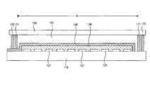
- FIG. 4is a schematic plane view of an organic electroluminescence display device according to the present invention.
- the organic electroluminescence display deviceincludes a first substrate 110 and a second substrate 150 .
- the second substrate 150has a smaller area than the first substrate 110 and exposes a part of the first substrate 110 .
- First and second sealants 171 and 172are formed between the first and second substrates 110 and 150 , and define an array region “B”.
- the second sealant 172surrounds the first sealant 171 .
- FIG. 5is a cross-sectional view of the organic electroluminescence display taken along the line V—V of FIG. 4 .
- a plurality of anode electrodes 121are formed in the array region “B” on the first substrate 110 , and an organic emissive layer 130 is formed on a plurality of the anode electrodes 121 .
- the first substrate 110is formed of a transparent material such as glass and plastics.
- the anode electrode 121has a high work function and is formed of a transparent conductive material.
- the anode electrodes 121may be formed of indium-tin-oxide (ITO) or indium-zinc-oxide (IZO).
- the emissive layer 130is formed of a single layer corresponding to the anode electrodes 121 .
- the organic emissive layer 130may be patterned to be a plurality of layers so as each of the patterned organic emissive layers 130 may correspond to each of the anode electrodes 121 .
- a cathode electrode 140is formed on the organic emissive layer 130 , and extends to one end of the first substrate 110 .
- the cathode electrode 140has a low work function and is formed of an opaque conductive material.
- the cathode electrode 140may include one of aluminum (Al), aluminum alloy, and calcium (Ca).
- a second substrate 150is arranged over and spaced apart from the first substrate 110 .
- the second substrate 150may be formed of a transparent material such as glass and plastics.
- a first sealant 171is formed between the first and second substrates 110 and 150
- a second sealant 172is formed at the outside of the first sealant 171 between the first and second substrates 110 and 150 .
- the first and second sealants 171 and 172form an airtight space 160 between the first and second substrates 110 and 150 , so that the organic emissive layer 130 is protected from external moisture and air.
- the airtight space 160is filled with an inert gas such as nitrogen (N 2 ).
- Parts of the first and second sealants 171 and 172may be disposed between the second substrate 150 and the extended portion of the cathode electrode 140 .
- a desiccantmay be formed on the inner surface of the second substrate 150 .
- a canister as a sealing elementmay be used in place of the second substrate 150 .
- the organic electroluminescence display deviceis airtight with double sealants 171 and 172 . Therefore, although the organic electroluminescence display device has a larger area, it prevents moisture or air from coming into the airtight space 160 through the gaps between the sealants 171 and 172 and the first substrate 110 and between the sealants 171 and 172 and the second substrate 150 . Accordingly, lifetime and reliability of the device increase.
Landscapes
- Physics & Mathematics (AREA)
- Optics & Photonics (AREA)
- Electroluminescent Light Sources (AREA)
Abstract
Description
Claims (22)
Applications Claiming Priority (2)
| Application Number | Priority Date | Filing Date | Title |
|---|---|---|---|
| KR1020010087425AKR100819864B1 (en) | 2001-12-28 | 2001-12-28 | Organic electroluminescent device |
| KRP2001-087425 | 2001-12-28 |
Publications (2)
| Publication Number | Publication Date |
|---|---|
| US20030127976A1 US20030127976A1 (en) | 2003-07-10 |
| US6861801B2true US6861801B2 (en) | 2005-03-01 |
Family
ID=19717848
Family Applications (1)
| Application Number | Title | Priority Date | Filing Date |
|---|---|---|---|
| US10/327,994Expired - LifetimeUS6861801B2 (en) | 2001-12-28 | 2002-12-26 | Organic electroluminescence display device having sealing structure and method of fabricating the same |
Country Status (2)
| Country | Link |
|---|---|
| US (1) | US6861801B2 (en) |
| KR (1) | KR100819864B1 (en) |
Cited By (23)
| Publication number | Priority date | Publication date | Assignee | Title |
|---|---|---|---|---|
| US20050269926A1 (en)* | 2004-05-27 | 2005-12-08 | Nobuhiko Fukuoka | Organic electroluminescence display apparatus and method for manufacturing the same |
| US20060274773A1 (en)* | 2005-06-07 | 2006-12-07 | Cohen Earl T | Method and apparatus for using meta-packets in a packet processing system |
| US20070170857A1 (en)* | 2006-01-25 | 2007-07-26 | Dong Soo Choi | Organic light-emitting display device and method of manufacturing the same |
| US20070170324A1 (en)* | 2006-01-25 | 2007-07-26 | Jae Sun Lee | Organic light emitting display and fabricating method of the same |
| US20070170423A1 (en)* | 2006-01-24 | 2007-07-26 | Choi Dong S | Organic light-emitting display and method of making the same |
| US20070170859A1 (en)* | 2006-01-25 | 2007-07-26 | Dong Soo Choi | Organic light emitting display and method of fabricating the same |
| US20070173167A1 (en)* | 2006-01-26 | 2007-07-26 | Young Seo Choi | Organic light-emitting display device and method of fabricating the same |
| US20070170839A1 (en)* | 2006-01-20 | 2007-07-26 | Choi Dong S | Organic light-emitting display device with frit seal and reinforcing structure |
| US20070170845A1 (en)* | 2006-01-26 | 2007-07-26 | Dong Soo Choi | Organic light emitting display device |
| US20070176549A1 (en)* | 2006-01-27 | 2007-08-02 | Jin Woo Park | Organic light emitting display and method of fabricating the same |
| US20070177069A1 (en)* | 2006-01-27 | 2007-08-02 | Jong Woo Lee | Organic light emitting display and fabricating method of the same |
| US20070247068A1 (en)* | 2006-04-20 | 2007-10-25 | Jin Woo Park | Organic light emitting display device and method of manufacturing the same |
| US20080012476A1 (en)* | 2006-06-30 | 2008-01-17 | Lg Philips Lcd Co., Ltd. | Organic electro-luminescence display device and method for fabricating the same |
| US20100013384A1 (en)* | 2008-07-17 | 2010-01-21 | Samsung Sdi Co., Ltd | Organic light-emitting display device and method of manufacturing the same |
| US7834550B2 (en) | 2006-01-24 | 2010-11-16 | Samsung Mobile Display Co., Ltd. | Organic light emitting display and fabricating method of the same |
| US7837530B2 (en) | 2006-03-29 | 2010-11-23 | Samsung Mobile Display Co., Ltd. | Method of sealing an organic light emitting display by means of a glass frit seal assembly |
| US20110014427A1 (en)* | 2009-07-17 | 2011-01-20 | Burgess Debra L | Methods for forming fritted cover sheets and glass packages comprising the same |
| US20110043495A1 (en)* | 2009-08-20 | 2011-02-24 | Hyun-Chol Bang | Organic light emitting display device |
| US7944143B2 (en) | 2006-01-25 | 2011-05-17 | Samsung Mobile Display Co., Ltd. | Organic light-emitting display device with frit seal and reinforcing structure bonded to frame |
| US8038495B2 (en) | 2006-01-20 | 2011-10-18 | Samsung Mobile Display Co., Ltd. | Organic light-emitting display device and manufacturing method of the same |
| US8120249B2 (en) | 2006-01-23 | 2012-02-21 | Samsung Mobile Display Co., Ltd. | Organic light emitting display and method of fabricating the same |
| US8299705B2 (en) | 2006-01-26 | 2012-10-30 | Samsung Display Co., Ltd. | Organic light emitting display device and manufacturing method thereof |
| US8729796B2 (en) | 2006-01-25 | 2014-05-20 | Samsung Display Co., Ltd. | Organic light emitting display device including a gap to improve image quality and method of fabricating the same |
Families Citing this family (13)
| Publication number | Priority date | Publication date | Assignee | Title |
|---|---|---|---|---|
| FI107859B (en)* | 1998-03-23 | 2001-10-15 | Nokia Networks Oy | Ordering services in a mobile communication system |
| KR101010372B1 (en)* | 2003-12-30 | 2011-01-21 | 엘지디스플레이 주식회사 | Organic electroluminescent device and manufacturing method thereof |
| KR100617117B1 (en)* | 2004-08-17 | 2006-08-31 | 엘지전자 주식회사 | Memory card mounting device of mobile communication terminal |
| KR20060023634A (en)* | 2004-09-10 | 2006-03-15 | (주)케이디티 | Front organic light emitting device and its manufacturing method |
| KR100700850B1 (en)* | 2005-03-21 | 2007-03-29 | 삼성에스디아이 주식회사 | Light-emitting display device and manufacturing method |
| US20070172971A1 (en)* | 2006-01-20 | 2007-07-26 | Eastman Kodak Company | Desiccant sealing arrangement for OLED devices |
| JP5268262B2 (en)* | 2006-02-24 | 2013-08-21 | キヤノン株式会社 | Electroluminescence display device |
| US8330339B2 (en) | 2007-06-28 | 2012-12-11 | Samsung Display Co., Ltd. | Light emitting display and method of manufacturing the same |
| US8258696B2 (en) | 2007-06-28 | 2012-09-04 | Samsung Mobile Display Co., Ltd. | Light emitting display and method of manufacturing the same |
| US8016631B2 (en)* | 2007-11-16 | 2011-09-13 | Global Oled Technology Llc | Desiccant sealing arrangement for OLED devices |
| US7948178B2 (en)* | 2009-03-04 | 2011-05-24 | Global Oled Technology Llc | Hermetic seal |
| KR101074812B1 (en)* | 2010-01-05 | 2011-10-19 | 삼성모바일디스플레이주식회사 | Organic light-emitting display device and manufacturing method of the same |
| KR102296916B1 (en)* | 2014-10-16 | 2021-09-02 | 삼성디스플레이 주식회사 | Organic light emitting display device |
Citations (3)
| Publication number | Priority date | Publication date | Assignee | Title |
|---|---|---|---|---|
| JP2001267065A (en)* | 2000-03-22 | 2001-09-28 | Casio Comput Co Ltd | EL device |
| US6635989B1 (en)* | 1998-08-03 | 2003-10-21 | E. I. Du Pont De Nemours And Company | Encapsulation of polymer-based solid state devices with inorganic materials |
| US6717052B2 (en)* | 2001-12-28 | 2004-04-06 | Delta Optoelectronics, Inc. | Housing structure with multiple sealing layers |
Family Cites Families (2)
| Publication number | Priority date | Publication date | Assignee | Title |
|---|---|---|---|---|
| KR20010097540A (en)* | 2000-04-24 | 2001-11-08 | 구자홍 | organic eletroluminescence display panel and method for fabricating the same |
| JP2001338755A (en)* | 2000-03-21 | 2001-12-07 | Seiko Epson Corp | Organic EL device and method of manufacturing the same |
- 2001
- 2001-12-28KRKR1020010087425Apatent/KR100819864B1/ennot_activeExpired - Lifetime
- 2002
- 2002-12-26USUS10/327,994patent/US6861801B2/ennot_activeExpired - Lifetime
Patent Citations (3)
| Publication number | Priority date | Publication date | Assignee | Title |
|---|---|---|---|---|
| US6635989B1 (en)* | 1998-08-03 | 2003-10-21 | E. I. Du Pont De Nemours And Company | Encapsulation of polymer-based solid state devices with inorganic materials |
| JP2001267065A (en)* | 2000-03-22 | 2001-09-28 | Casio Comput Co Ltd | EL device |
| US6717052B2 (en)* | 2001-12-28 | 2004-04-06 | Delta Optoelectronics, Inc. | Housing structure with multiple sealing layers |
Cited By (35)
| Publication number | Priority date | Publication date | Assignee | Title |
|---|---|---|---|---|
| US20050269926A1 (en)* | 2004-05-27 | 2005-12-08 | Nobuhiko Fukuoka | Organic electroluminescence display apparatus and method for manufacturing the same |
| US7306346B2 (en)* | 2004-05-27 | 2007-12-11 | Hitachi Displays, Ltd. | Organic electroluminescence display apparatus and method for manufacturing the same |
| US20060274773A1 (en)* | 2005-06-07 | 2006-12-07 | Cohen Earl T | Method and apparatus for using meta-packets in a packet processing system |
| US8415880B2 (en) | 2006-01-20 | 2013-04-09 | Samsung Display Co., Ltd. | Organic light-emitting display device with frit seal and reinforcing structure |
| US8038495B2 (en) | 2006-01-20 | 2011-10-18 | Samsung Mobile Display Co., Ltd. | Organic light-emitting display device and manufacturing method of the same |
| US9004972B2 (en) | 2006-01-20 | 2015-04-14 | Samsung Display Co., Ltd. | Organic light-emitting display device with frit seal and reinforcing structure |
| US20070170839A1 (en)* | 2006-01-20 | 2007-07-26 | Choi Dong S | Organic light-emitting display device with frit seal and reinforcing structure |
| US8120249B2 (en) | 2006-01-23 | 2012-02-21 | Samsung Mobile Display Co., Ltd. | Organic light emitting display and method of fabricating the same |
| US20070170423A1 (en)* | 2006-01-24 | 2007-07-26 | Choi Dong S | Organic light-emitting display and method of making the same |
| US7834550B2 (en) | 2006-01-24 | 2010-11-16 | Samsung Mobile Display Co., Ltd. | Organic light emitting display and fabricating method of the same |
| US8729796B2 (en) | 2006-01-25 | 2014-05-20 | Samsung Display Co., Ltd. | Organic light emitting display device including a gap to improve image quality and method of fabricating the same |
| US8164257B2 (en) | 2006-01-25 | 2012-04-24 | Samsung Mobile Display Co., Ltd. | Organic light emitting display and method of fabricating the same |
| US20070170859A1 (en)* | 2006-01-25 | 2007-07-26 | Dong Soo Choi | Organic light emitting display and method of fabricating the same |
| US7825594B2 (en) | 2006-01-25 | 2010-11-02 | Samsung Mobile Display Co., Ltd. | Organic light emitting display and fabricating method of the same |
| US20070170324A1 (en)* | 2006-01-25 | 2007-07-26 | Jae Sun Lee | Organic light emitting display and fabricating method of the same |
| US20070170857A1 (en)* | 2006-01-25 | 2007-07-26 | Dong Soo Choi | Organic light-emitting display device and method of manufacturing the same |
| US7944143B2 (en) | 2006-01-25 | 2011-05-17 | Samsung Mobile Display Co., Ltd. | Organic light-emitting display device with frit seal and reinforcing structure bonded to frame |
| US8063561B2 (en)* | 2006-01-26 | 2011-11-22 | Samsung Mobile Display Co., Ltd. | Organic light emitting display device |
| US8299705B2 (en) | 2006-01-26 | 2012-10-30 | Samsung Display Co., Ltd. | Organic light emitting display device and manufacturing method thereof |
| US20070173167A1 (en)* | 2006-01-26 | 2007-07-26 | Young Seo Choi | Organic light-emitting display device and method of fabricating the same |
| US20070170845A1 (en)* | 2006-01-26 | 2007-07-26 | Dong Soo Choi | Organic light emitting display device |
| US20070176549A1 (en)* | 2006-01-27 | 2007-08-02 | Jin Woo Park | Organic light emitting display and method of fabricating the same |
| US20070177069A1 (en)* | 2006-01-27 | 2007-08-02 | Jong Woo Lee | Organic light emitting display and fabricating method of the same |
| US7821197B2 (en)* | 2006-01-27 | 2010-10-26 | Samsung Mobile Display Co., Ltd. | Organic light emitting display and fabricating method of the same |
| US7837530B2 (en) | 2006-03-29 | 2010-11-23 | Samsung Mobile Display Co., Ltd. | Method of sealing an organic light emitting display by means of a glass frit seal assembly |
| US20070247068A1 (en)* | 2006-04-20 | 2007-10-25 | Jin Woo Park | Organic light emitting display device and method of manufacturing the same |
| US7749039B2 (en)* | 2006-04-20 | 2010-07-06 | Samsung Mobile Display Co., Ltd. | Organic light emitting display device and method of manufacturing the same |
| US20080012476A1 (en)* | 2006-06-30 | 2008-01-17 | Lg Philips Lcd Co., Ltd. | Organic electro-luminescence display device and method for fabricating the same |
| US8221178B2 (en)* | 2006-06-30 | 2012-07-17 | Lg Philips Lcd Co., Ltd. | Method for fabricating organic electro-luminescence display device |
| US20100013384A1 (en)* | 2008-07-17 | 2010-01-21 | Samsung Sdi Co., Ltd | Organic light-emitting display device and method of manufacturing the same |
| US8304989B2 (en)* | 2008-07-17 | 2012-11-06 | Samsung Display Co., Ltd. | Organic light-emitting display device and method of manufacturing the same |
| US20110014427A1 (en)* | 2009-07-17 | 2011-01-20 | Burgess Debra L | Methods for forming fritted cover sheets and glass packages comprising the same |
| US8505337B2 (en)* | 2009-07-17 | 2013-08-13 | Corning Incorporated | Methods for forming fritted cover sheets and glass packages comprising the same |
| US20110043495A1 (en)* | 2009-08-20 | 2011-02-24 | Hyun-Chol Bang | Organic light emitting display device |
| US8432334B2 (en)* | 2009-08-20 | 2013-04-30 | Samsung Display Co., Ltd. | Organic light emitting display device |
Also Published As
| Publication number | Publication date |
|---|---|
| KR100819864B1 (en) | 2008-04-07 |
| US20030127976A1 (en) | 2003-07-10 |
| KR20030057053A (en) | 2003-07-04 |
Similar Documents
| Publication | Publication Date | Title |
|---|---|---|
| US6861801B2 (en) | Organic electroluminescence display device having sealing structure and method of fabricating the same | |
| US7755279B2 (en) | Organic electroluminescent device and fabricating method thereof | |
| US6922015B2 (en) | Organic electroluminescent display device and method of fabricating the same | |
| US8093804B2 (en) | Organic electroluminescent display device having a novel concept for luminous efficiency | |
| US8198624B2 (en) | Organic light emitting device | |
| KR100623451B1 (en) | Organic electroluminescent display device and manufacturing method thereof | |
| KR100834341B1 (en) | Active matrix organic electroluminescent device | |
| KR100623449B1 (en) | Organic electroluminescent display device and manufacturing method thereof | |
| KR100638139B1 (en) | Organic electroluminescent display device and manufacturing method thereof | |
| US20030139112A1 (en) | Method of fabricating organic electroluminescence display device | |
| KR100712122B1 (en) | Flat Panel Display | |
| KR100783359B1 (en) | Organic electroluminescent device | |
| KR100684855B1 (en) | Organic light emitting display | |
| KR100961954B1 (en) | Organic light emitting display manufacturing method | |
| KR100501705B1 (en) | Organic Electro Luminescence Display including External Force Interception Shield | |
| KR100765530B1 (en) | Top emission type electroluminescent device and method of manufacturing same | |
| KR20030083455A (en) | Organic Electro-Luminescence Device | |
| KR100692846B1 (en) | Organic electroluminescent display device and manufacturing method thereof | |
| KR100414296B1 (en) | Packaging structure of organic electro luminescent display and its fabrication method | |
| KR101010372B1 (en) | Organic electroluminescent device and manufacturing method thereof | |
| KR20050077923A (en) | Electro-luminescence display device | |
| KR101157227B1 (en) | top emission type Organic Electro luminescence Device and fabrication method thereof | |
| KR100726954B1 (en) | Organic light emitting display device and manufacturing method | |
| JP2009246065A (en) | Organic el element | |
| KR20050106138A (en) | Organic electro-luminescence display device and fabricating method thereof |
Legal Events
| Date | Code | Title | Description |
|---|---|---|---|
| AS | Assignment | Owner name:LG.PHILIPS LCD CO., LTD., KOREA, REPUBLIC OF Free format text:ASSIGNMENT OF ASSIGNORS INTEREST;ASSIGNORS:KIM, KWAN-SOO;PARK, JAE-YONG;REEL/FRAME:013626/0928 Effective date:20021220 | |
| FEPP | Fee payment procedure | Free format text:PAYOR NUMBER ASSIGNED (ORIGINAL EVENT CODE: ASPN); ENTITY STATUS OF PATENT OWNER: LARGE ENTITY | |
| STCF | Information on status: patent grant | Free format text:PATENTED CASE | |
| AS | Assignment | Owner name:LG DISPLAY CO., LTD., KOREA, REPUBLIC OF Free format text:CHANGE OF NAME;ASSIGNOR:LG.PHILIPS LCD CO., LTD.;REEL/FRAME:021147/0009 Effective date:20080319 Owner name:LG DISPLAY CO., LTD.,KOREA, REPUBLIC OF Free format text:CHANGE OF NAME;ASSIGNOR:LG.PHILIPS LCD CO., LTD.;REEL/FRAME:021147/0009 Effective date:20080319 | |
| FPAY | Fee payment | Year of fee payment:4 | |
| FEPP | Fee payment procedure | Free format text:PAYER NUMBER DE-ASSIGNED (ORIGINAL EVENT CODE: RMPN); ENTITY STATUS OF PATENT OWNER: LARGE ENTITY Free format text:PAYOR NUMBER ASSIGNED (ORIGINAL EVENT CODE: ASPN); ENTITY STATUS OF PATENT OWNER: LARGE ENTITY | |
| FPAY | Fee payment | Year of fee payment:8 | |
| FPAY | Fee payment | Year of fee payment:12 |