US6861735B2 - Resin molded type semiconductor device and a method of manufacturing the same - Google Patents
Resin molded type semiconductor device and a method of manufacturing the sameDownload PDFInfo
- Publication number
- US6861735B2 US6861735B2US10/747,982US74798203AUS6861735B2US 6861735 B2US6861735 B2US 6861735B2US 74798203 AUS74798203 AUS 74798203AUS 6861735 B2US6861735 B2US 6861735B2
- Authority
- US
- United States
- Prior art keywords
- semiconductor device
- type semiconductor
- resin molded
- lead portions
- inner lead
- Prior art date
- Legal status (The legal status is an assumption and is not a legal conclusion. Google has not performed a legal analysis and makes no representation as to the accuracy of the status listed.)
- Expired - Lifetime
Links
Images


Classifications
- H—ELECTRICITY
- H01—ELECTRIC ELEMENTS
- H01L—SEMICONDUCTOR DEVICES NOT COVERED BY CLASS H10
- H01L23/00—Details of semiconductor or other solid state devices
- H01L23/48—Arrangements for conducting electric current to or from the solid state body in operation, e.g. leads, terminal arrangements ; Selection of materials therefor
- H01L23/488—Arrangements for conducting electric current to or from the solid state body in operation, e.g. leads, terminal arrangements ; Selection of materials therefor consisting of soldered or bonded constructions
- H01L23/495—Lead-frames or other flat leads
- H01L23/49541—Geometry of the lead-frame
- H—ELECTRICITY
- H01—ELECTRIC ELEMENTS
- H01L—SEMICONDUCTOR DEVICES NOT COVERED BY CLASS H10
- H01L23/00—Details of semiconductor or other solid state devices
- H01L23/28—Encapsulations, e.g. encapsulating layers, coatings, e.g. for protection
- H01L23/31—Encapsulations, e.g. encapsulating layers, coatings, e.g. for protection characterised by the arrangement or shape
- H01L23/3107—Encapsulations, e.g. encapsulating layers, coatings, e.g. for protection characterised by the arrangement or shape the device being completely enclosed
- H—ELECTRICITY
- H01—ELECTRIC ELEMENTS
- H01L—SEMICONDUCTOR DEVICES NOT COVERED BY CLASS H10
- H01L23/00—Details of semiconductor or other solid state devices
- H01L23/48—Arrangements for conducting electric current to or from the solid state body in operation, e.g. leads, terminal arrangements ; Selection of materials therefor
- H01L23/488—Arrangements for conducting electric current to or from the solid state body in operation, e.g. leads, terminal arrangements ; Selection of materials therefor consisting of soldered or bonded constructions
- H01L23/495—Lead-frames or other flat leads
- H01L23/49541—Geometry of the lead-frame
- H01L23/49548—Cross section geometry
- H—ELECTRICITY
- H01—ELECTRIC ELEMENTS
- H01L—SEMICONDUCTOR DEVICES NOT COVERED BY CLASS H10
- H01L2224/00—Indexing scheme for arrangements for connecting or disconnecting semiconductor or solid-state bodies and methods related thereto as covered by H01L24/00
- H01L2224/01—Means for bonding being attached to, or being formed on, the surface to be connected, e.g. chip-to-package, die-attach, "first-level" interconnects; Manufacturing methods related thereto
- H01L2224/42—Wire connectors; Manufacturing methods related thereto
- H01L2224/44—Structure, shape, material or disposition of the wire connectors prior to the connecting process
- H01L2224/45—Structure, shape, material or disposition of the wire connectors prior to the connecting process of an individual wire connector
- H01L2224/45001—Core members of the connector
- H01L2224/45099—Material
- H01L2224/451—Material with a principal constituent of the material being a metal or a metalloid, e.g. boron (B), silicon (Si), germanium (Ge), arsenic (As), antimony (Sb), tellurium (Te) and polonium (Po), and alloys thereof
- H—ELECTRICITY
- H01—ELECTRIC ELEMENTS
- H01L—SEMICONDUCTOR DEVICES NOT COVERED BY CLASS H10
- H01L2224/00—Indexing scheme for arrangements for connecting or disconnecting semiconductor or solid-state bodies and methods related thereto as covered by H01L24/00
- H01L2224/01—Means for bonding being attached to, or being formed on, the surface to be connected, e.g. chip-to-package, die-attach, "first-level" interconnects; Manufacturing methods related thereto
- H01L2224/42—Wire connectors; Manufacturing methods related thereto
- H01L2224/47—Structure, shape, material or disposition of the wire connectors after the connecting process
- H01L2224/48—Structure, shape, material or disposition of the wire connectors after the connecting process of an individual wire connector
- H01L2224/4805—Shape
- H01L2224/4809—Loop shape
- H01L2224/48091—Arched
- H—ELECTRICITY
- H01—ELECTRIC ELEMENTS
- H01L—SEMICONDUCTOR DEVICES NOT COVERED BY CLASS H10
- H01L2224/00—Indexing scheme for arrangements for connecting or disconnecting semiconductor or solid-state bodies and methods related thereto as covered by H01L24/00
- H01L2224/01—Means for bonding being attached to, or being formed on, the surface to be connected, e.g. chip-to-package, die-attach, "first-level" interconnects; Manufacturing methods related thereto
- H01L2224/42—Wire connectors; Manufacturing methods related thereto
- H01L2224/47—Structure, shape, material or disposition of the wire connectors after the connecting process
- H01L2224/48—Structure, shape, material or disposition of the wire connectors after the connecting process of an individual wire connector
- H01L2224/481—Disposition
- H01L2224/48151—Connecting between a semiconductor or solid-state body and an item not being a semiconductor or solid-state body, e.g. chip-to-substrate, chip-to-passive
- H01L2224/48221—Connecting between a semiconductor or solid-state body and an item not being a semiconductor or solid-state body, e.g. chip-to-substrate, chip-to-passive the body and the item being stacked
- H01L2224/48245—Connecting between a semiconductor or solid-state body and an item not being a semiconductor or solid-state body, e.g. chip-to-substrate, chip-to-passive the body and the item being stacked the item being metallic
- H01L2224/48247—Connecting between a semiconductor or solid-state body and an item not being a semiconductor or solid-state body, e.g. chip-to-substrate, chip-to-passive the body and the item being stacked the item being metallic connecting the wire to a bond pad of the item
- H—ELECTRICITY
- H01—ELECTRIC ELEMENTS
- H01L—SEMICONDUCTOR DEVICES NOT COVERED BY CLASS H10
- H01L2224/00—Indexing scheme for arrangements for connecting or disconnecting semiconductor or solid-state bodies and methods related thereto as covered by H01L24/00
- H01L2224/01—Means for bonding being attached to, or being formed on, the surface to be connected, e.g. chip-to-package, die-attach, "first-level" interconnects; Manufacturing methods related thereto
- H01L2224/42—Wire connectors; Manufacturing methods related thereto
- H01L2224/47—Structure, shape, material or disposition of the wire connectors after the connecting process
- H01L2224/49—Structure, shape, material or disposition of the wire connectors after the connecting process of a plurality of wire connectors
- H01L2224/491—Disposition
- H01L2224/4912—Layout
- H01L2224/49171—Fan-out arrangements
- H—ELECTRICITY
- H01—ELECTRIC ELEMENTS
- H01L—SEMICONDUCTOR DEVICES NOT COVERED BY CLASS H10
- H01L2224/00—Indexing scheme for arrangements for connecting or disconnecting semiconductor or solid-state bodies and methods related thereto as covered by H01L24/00
- H01L2224/73—Means for bonding being of different types provided for in two or more of groups H01L2224/10, H01L2224/18, H01L2224/26, H01L2224/34, H01L2224/42, H01L2224/50, H01L2224/63, H01L2224/71
- H01L2224/732—Location after the connecting process
- H01L2224/73251—Location after the connecting process on different surfaces
- H01L2224/73265—Layer and wire connectors
- H—ELECTRICITY
- H01—ELECTRIC ELEMENTS
- H01L—SEMICONDUCTOR DEVICES NOT COVERED BY CLASS H10
- H01L24/00—Arrangements for connecting or disconnecting semiconductor or solid-state bodies; Methods or apparatus related thereto
- H01L24/01—Means for bonding being attached to, or being formed on, the surface to be connected, e.g. chip-to-package, die-attach, "first-level" interconnects; Manufacturing methods related thereto
- H01L24/42—Wire connectors; Manufacturing methods related thereto
- H01L24/44—Structure, shape, material or disposition of the wire connectors prior to the connecting process
- H01L24/45—Structure, shape, material or disposition of the wire connectors prior to the connecting process of an individual wire connector
- H—ELECTRICITY
- H01—ELECTRIC ELEMENTS
- H01L—SEMICONDUCTOR DEVICES NOT COVERED BY CLASS H10
- H01L24/00—Arrangements for connecting or disconnecting semiconductor or solid-state bodies; Methods or apparatus related thereto
- H01L24/01—Means for bonding being attached to, or being formed on, the surface to be connected, e.g. chip-to-package, die-attach, "first-level" interconnects; Manufacturing methods related thereto
- H01L24/42—Wire connectors; Manufacturing methods related thereto
- H01L24/47—Structure, shape, material or disposition of the wire connectors after the connecting process
- H01L24/48—Structure, shape, material or disposition of the wire connectors after the connecting process of an individual wire connector
- H—ELECTRICITY
- H01—ELECTRIC ELEMENTS
- H01L—SEMICONDUCTOR DEVICES NOT COVERED BY CLASS H10
- H01L24/00—Arrangements for connecting or disconnecting semiconductor or solid-state bodies; Methods or apparatus related thereto
- H01L24/01—Means for bonding being attached to, or being formed on, the surface to be connected, e.g. chip-to-package, die-attach, "first-level" interconnects; Manufacturing methods related thereto
- H01L24/42—Wire connectors; Manufacturing methods related thereto
- H01L24/47—Structure, shape, material or disposition of the wire connectors after the connecting process
- H01L24/49—Structure, shape, material or disposition of the wire connectors after the connecting process of a plurality of wire connectors
- H—ELECTRICITY
- H01—ELECTRIC ELEMENTS
- H01L—SEMICONDUCTOR DEVICES NOT COVERED BY CLASS H10
- H01L2924/00—Indexing scheme for arrangements or methods for connecting or disconnecting semiconductor or solid-state bodies as covered by H01L24/00
- H01L2924/0001—Technical content checked by a classifier
- H01L2924/00014—Technical content checked by a classifier the subject-matter covered by the group, the symbol of which is combined with the symbol of this group, being disclosed without further technical details
- H—ELECTRICITY
- H01—ELECTRIC ELEMENTS
- H01L—SEMICONDUCTOR DEVICES NOT COVERED BY CLASS H10
- H01L2924/00—Indexing scheme for arrangements or methods for connecting or disconnecting semiconductor or solid-state bodies as covered by H01L24/00
- H01L2924/15—Details of package parts other than the semiconductor or other solid state devices to be connected
- H01L2924/181—Encapsulation
Definitions
- the inventionrelates to a resin molded type semiconductor device in which a semiconductor chip is mounted on a lead frame and the outer periphery of the semiconductor chip, particularly, the upper face of the semiconductor chip is molded by a sealing resin, and also to a method of manufacturing the semiconductor device.
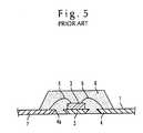
- FIG. 5is a section view showing a resin molded type semiconductor device of the prior art.
- a semiconductor chip 3is mounted on a die pad portion 2 of a lead frame 1 , and terminals (not shown) of the semiconductor chip 3 are electrically connected to inner lead portions 4 of the lead frame 1 by thin metal wires 5 .
- the outer peripheral region of the semiconductor chip 3is molded by a sealing resin 6 .
- a resin molded type semiconductor device produced so as to have a structure such as shown in FIG. 5is provided with a structure in which an outer lead portion 7 serving as external terminals is arranged on a bottom face of the semiconductor device. Since only the face of the lead frame 1 on which the semiconductor chip 3 is mounted is molded by the sealing resin 6 and the rear face of the lead frame 1 is not substantially molded, it is possible to realize a thin resin molded type semiconductor device.
- a tapered shapeis first formed at tip end portions of the inner lead portions 4 of the lead frame 1 by mechanical or chemical working, and the semiconductor chip 3 is then bonded onto the lead frame 1 . Thereafter, the semiconductor chip 3 is electrically connected to the inner lead portions 4 of the lead frame 1 by the thin metal wires 5 , and the face of the lead frame 1 for mounting the semiconductor chip 3 is then molded by the sealing resin 6 by means of transfer molding. In order to form external terminals, finally, the outer lead portion 7 of the lead frame 1 which projects from the sealing resin 6 is worked, thereby completing the resin molded type semiconductor device.
- an insulative resin tape 8 on which a semiconductor chip 3 is to be mountedis bonded to tip end portions 4 a of inner lead portions 4 of a lead frame 1 , thereby forming a die pad portion.
- the devicehas a structure in which, after the semiconductor chip 3 is mounted on the resin tape 8 , terminals of the semiconductor chip 3 are electrically connected to the inner lead portions 4 by thin metal wires 5 , and the face of the lead frame 1 for mounting the semiconductor chip 3 is molded by a sealing resin 6 .
- the resin molded type semiconductor device shown in FIG. 6has the merit that the device can be made thinner than the resin molded type semiconductor device shown in FIG. 5 . Specifically, in the resin molded type semiconductor device shown in FIG.
- the resin tape 8is bonded to the lower faces of the inner lead portions 4 of the lead frame 1 and the semiconductor chip 3 is mounted on the upper face of the portion. Therefore, the step difference between the upper faces of the inner lead portions 4 and the upper face of the semiconductor chip 3 is reduced. As a result, also the resin thickness of the sealing resin 6 is reduced, and the resulting resin molded type semiconductor device has a reduced thickness.
- the thickness of the sealing resin 6cannot be reduced by such a degree that is attained in the resin molded type semiconductor device shown in FIG. 6 .
- a resin molded type semiconductor device of the prior arthas a structure in which substantially only the face of a lead frame on which a semiconductor chip is mounted, i.e., the upper face of the lead frame is molded by a sealing resin. Even when a tapered shape is formed in an inner lead portion, therefore, the contact area between the lead frame and the sealing resin is reduced as a whole, thereby producing a problem in that the adhesiveness is impaired and the reliability of a product is lowered. Since such a device has a structure in which substantially only the single face of the lead frame is resin-molded, there are further problems in that the semiconductor chip is adversely affected by stress of the sealing resin, and that package crack occurs in the sealing resin.
- the resin molded type semiconductor device of the inventioncomprises: a semiconductor chip which is mounted on a die pad portion of a lead frame; thin metal wires which electrically connect terminals of an upper face of the semiconductor chip to inner lead portions of the lead frame; a sealing resin which seals an outer peripheral region of the semiconductor chip, the region including a thin metal wire region of the upper face of the semiconductor chip, and a lower region of the die pad portion; and outer lead portions which are arranged in a bottom face region of the sealing resin, and is characterized in that the lead frame is subjected to an upsetting process so that the die pad portion is located at a position higher than the inner lead portions.
- the lead frameis subjected to an upsetting process so that the die pad portion is located at a position higher than the inner lead portions. Therefore, the sealing resin of a thickness corresponding to the step difference of the upsetting exists below the die pad portion, the adhesiveness between the lead frame and the sealing resin can be improved, and the reliability of a product can be maintained. Even when both the faces, or the upper and lower faces of the lead frame are resin-molded, the thickness of the resin of the lower face is equal to a value corresponding to the step difference of the upsetting. Consequently, the thinning can be realized.
- the resin molded type semiconductor device of the inventioncomprises: a semiconductor chip which is mounted on a die pad portion of a lead frame; thin metal wires which electrically connect terminals of an upper face of the semiconductor chip to inner lead portions of the lead frame; a sealing resin which seals an outer peripheral region of the semiconductor chip, the region including a thin metal wire region of the upper face of the semiconductor chip; and outer lead portions which are arranged in a bottom face region of the sealing resin and which are formed to be continuous to the respective inner lead portions, wherein at least one groove portion is formed in a surface of each of the inner lead portions.
- At least one groove portionis formed in the surface of each of the inner lead portions. Therefore, the anchoring effect to the sealing resin can be improved, stress acting on a lead portion of a product, and stress to the thin metal wires can be relaxed, and leads and the thin metal wires can be prevented from peeling off. Consequently, the reliability of a product can be maintained.
- the resin molded type semiconductor device of the inventioncomprises: a semiconductor chip which is mounted on a die pad portion of a lead frame; thin metal wires which electrically connect terminals of an upper face of the semiconductor chip to inner lead portions of the lead frame; a sealing resin which seals an outer peripheral region of the semiconductor chip, the region including a thin metal wire region of the upper face of the semiconductor chip; and outer lead portions which are arranged in a bottom face region of the sealing resin and which are formed to be continuous to the respective inner lead portions, and is characterized in that a plurality of groove portions are formed in a surface of each of the inner lead portions, and a connecting portion of the thin metal wire on a side of the inner lead portion is disposed between the groove portions.
- a plurality of groove portionsare formed in the surface of each of the inner lead portions, and a connecting portion of the thin metal wire on the side of the inner lead portion is disposed between the groove portions. Therefore, the anchoring effect to the sealing resin can be improved, stress acting on a lead portion of a product, and stress to the thin metal wires can be relaxed, and leads and the thin metal wires can be prevented from peeling off. In this case, stress due to the structure in which the single face of the lead frame is molded by the sealing resin is absorbed by the groove portions, and does not act on an area between the groove portions. Therefore, the connecting portions of the thin metal wires are not broken and stable connection is enabled.
- the resin molded type semiconductor device of the inventioncomprises: a semiconductor chip which is mounted on a die pad portion of a lead frame; thin metal wires which electrically connect terminals of an upper face of the semiconductor chip to inner lead portions of the lead frame; a sealing resin which seals an outer peripheral region of the semiconductor chip, the region including a thin metal wire region of the upper face of the semiconductor chip; and outer lead portions which are arranged in a bottom face region of the sealing resin and which are formed to be continuous to the respective inner lead portions, and is characterized in that a widened portion is formed in each of the inner lead portions.
- the resin molded type semiconductor device of the inventioncomprises: a semiconductor chip which is mounted on a die pad portion of a lead frame; thin metal wires which electrically connect terminals of an upper face of the semiconductor chip to inner lead portions of the lead frame; a sealing resin which seals an outer peripheral region of the semiconductor chip, the region including a thin metal wire region of the upper face of the semiconductor chip; and outer lead portions which are arranged in a bottom face region of the sealing resin and which are formed to be continuous to the respective inner lead portions, and is characterized in that a widened portion is formed in each of the inner lead portions and at least one groove portion is formed in a surface.
- a widened portionis formed in each of the inner lead portions and at least one groove portion is formed in the surface. Therefore, the anchoring effect to the sealing resin can be further improved, stress acting on a lead portion of a product, and stress to the thin metal wires can be further relaxed, and the effect of preventing leads and the thin metal wires from peeling off is enhanced.
- the resin molded type semiconductor device of the inventioncomprises: a semiconductor chip which is mounted on a die pad portion of a lead frame; thin metal wires which electrically connect terminals of an upper face of the semiconductor chip to inner lead portions of the lead frame; a sealing resin which seals an outer peripheral region of the semiconductor chip, the region including a thin metal wire region of the upper face of the semiconductor chip; and outer lead portions which are arranged in a bottom face region of the sealing resin and which are formed to be continuous to each of the inner lead portions, and is characterized in that a widened portion is formed in each of the inner lead portions, a plurality of groove portions are formed in a surface, and connecting portions of the thin metal wires on a side of the inner lead portion are disposed between the groove portions.
- a widened portionis formed in each of the inner lead portions, a plurality of groove portions are formed in the surface, and connecting portions of the thin metal wires on a side of the inner lead portion are disposed between the groove portions. Therefore, the anchoring effect to the sealing resin can be further improved, stress acting on a lead portion of a product, and stress to the thin metal wires can be further relaxed, and the effect of preventing leads and the thin metal wires from peeling off is enhanced. In this case, when two or more groove portions are disposed and the thin metal wires are connected to an area between the groove portions, the effect of absorbing stress can be enhanced.
- exposed faces of the outer lead portionsare arranged in a same level as an outer face of the sealing resin.
- the exposed faces of the outer lead portionsare arranged in the same level as the outer face of the sealing resin.
- the outer lead portionscan be arranged so as to be embedded in the bottom face portion of the sealing resin, while the outer lead portions project from a side face of the sealing resin. Therefore, the reliability of the outer lead portions serving as external terminals can be improved, and it is possible to provide a resin molded type semiconductor device which is miniaturized by a size corresponding to the nonprojecting structure of the outer lead portions.
- the method of manufacturing a resin molded type semiconductor device of the inventioncomprises the steps of: performing an upsetting process on a lead frame so that a die pad portion is located at a position higher than inner lead portions; bonding a semiconductor chip to the die pad portion of the lead frame; electrically connecting terminals of the semiconductor chip to the inner lead portions of the lead frame by thin metal wires; sealing an outer peripheral region of the semiconductor chip, thereby forming a sealing resin, the region including a region of an upper face of the semiconductor chip and electrically connected by the thin metal wires, and a lower region of the die pad portion; and shaping outer lead portions of the lead frame so as to be exposed from an outer face of the sealing resin.
- the lead frameis subjected to an upsetting process so that the die pad portion is located at a position higher than the inner lead portions, and the outer peripheral region of the semiconductor chip including the region of the upper face of the semiconductor chip and electrically connected by the thin metal wires, and the lower region of the die pad portion is molded to form the sealing resin. Therefore, the sealing resin of a thickness corresponding to the step difference of the upsetting exists below the die pad portion, the adhesiveness between the lead frame and the sealing resin can be improved, and the reliability of a product can be maintained. Even when both the faces, or the upper and lower faces of the lead frame are resin-molded, the thickness of the resin of the lower face is equal to the thickness of the step difference of the upsetting. Consequently, the thinning can be realized.
- the method of manufacturing a resin molded type semiconductor device of the inventionis characterized in that the method comprises the steps of: bonding a semiconductor chip to a lead frame having inner lead portions in each of which a widened portion is disposed and at least one groove portion is formed in a surface; electrically connecting terminals of the semiconductor chip to the inner lead portions of the lead frame by thin metal wires; sealing an outer peripheral region of the semiconductor chip, thereby forming a sealing resin, the region including a region of an upper face of the semiconductor chip and electrically connected by the thin metal wires, and a lower region of the semiconductor chip; and shaping outer lead portions of the lead frame so as to be exposed from an outer face of the sealing resin, and, when the terminals of the semiconductor chip are to be electrically connected to the inner lead portions by the thin metal wires, the connection is performed while connecting portions of the thin metal wires on the side of the inner lead portions are disposed in the vicinity of the groove portion.
- the connectionis performed while connecting portions of the thin metal wires on the side of the inner lead portions are disposed in the vicinity of the groove portion. Therefore, stress due to the structure in which the single face of the lead frame is molded by the sealing resin is absorbed by the groove portion, the connecting portions of the thin metal wires are not broken, and stable connection is enabled. Moreover, the anchoring effect to the sealing resin can be improved, and stress acting on a lead portion of a product can be relaxed by the groove portion, and leads and the thin metal wires can be prevented from peeling off.
- the method of manufacturing a resin molded type semiconductor device of the inventionis characterized in that the method comprises the steps of: bonding a semiconductor chip to a lead frame having inner lead portions in each of which a widened portion is disposed and a plurality of groove portions are formed in a surface; electrically connecting terminals of the semiconductor chip to the inner lead portions of the lead frame by thin metal wires; sealing an outer peripheral region of the semiconductor chip, thereby forming a sealing resin, the region including a region of an upper face of the semiconductor chip and electrically connected by the thin metal wires, and a lower region of the semiconductor chip; and shaping outer lead portions of the lead frame so as to be exposed from an outer face of the sealing resin, and, when the terminals of the semiconductor chip are to be electrically connected to the inner lead portions by the thin metal wires, the connection is performed while connecting portions of the thin metal wires on the side of the inner lead portions are disposed between the groove portions.
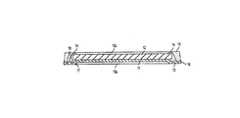
- FIG. 1is a section view shoving a resin molded type semiconductor device of an embodiment of the invention
- FIG. 1Aillustrates the resin contacting the bottom of the chip
- FIG. 2is a plan view showing the resin molded type semiconductor device of the embodiment of the invention.
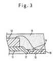
- FIG. 3is an enlarged section view of main portions of the resin molded type semiconductor device of the embodiment of the invention.
- FIG. 4 ( a )is a plan view of an inner lead portion of the resin molded type semiconductor device of the embodiment of the invention.
- FIG. 4 ( b )is a left side view
- FIG. 4 ( c )is a front view
- FIG. 5is a section view of a resin molded type semiconductor device of the prior art.
- FIG. 6is a section view showing another example of a resin molded type semiconductor device of the prior art.
- a resin molded type semiconductor device of an embodiment of the inventionwill be described with reference to FIGS. 1 to 4 .
- FIG. 1is a section view of the resin molded type semiconductor device of the embodiment of the invention
- FIG. 2is a plan view of the device
- FIG. 3is an enlarged section view showing an inner lead portion of the device
- FIG. 4 ( a )is an enlarged plan view showing a tip end of the inner lead portion
- FIG. 4 ( b )is a left side view
- FIG. 4 ( c )is a front view.
- the plan viewis a view which is obtained by partially removing away a sealing resin, in order to show the internal structure.
- broken linesshow a die pad portion and part of suspension leads.
- the resin molded type semiconductor devicecomprises: a semiconductor chip 12 which is mounted on a die pad portion 11 of a lead frame 9 and serving as a supporting portion of the semiconductor chip 12 supported by suspension leads 10 ; thin metal wires 14 which electrically connect terminals of the upper face of the semiconductor chip 12 to inner lead portions 13 of the lead frame 9 ; a sealing resin 15 which seals an outer peripheral region of the semiconductor chip 12 including a thin metal wire 14 region of the upper face of the semiconductor chip 12 , and a lower region of the die pad portion 11 ; and outer lead portions 16 which are arranged in a bottom face region of the sealing resin 15 , which are formed to be continuous to the respective inner lead portions 13 , and which serve as external terminals.
- the lead frame 9is subjected to an upsetting process so that the die pad portion 11 is located at a position higher than the inner lead portions 13 .
- the deviceis configured so that the die pad portion 11 is smaller in area than the semiconductor chip 12 to be mounted.
- the suspension leads 10are subjected to an upsetting process, and a step portion 17 is provided. Therefore, a sealing resin 15 a can exist also below the die pad portion 11 .
- the deviceis of the thin type, the device is a semiconductor device which is substantially of the double-side molding type with respect to the lead frame 9 .
- FIG. 1Ashows chip 12 wider than die pad portion 11 , with the resin 15 thus contacting the bottom of the chip. As noted below, there is contact through adhesiveness between the resin and the rear face of chip 12 .
- each of the inner lead portions 13has a widened portion 18 at a tip end portion, and a plurality of groove portions 19 are formed in the surface.
- a reverse taperis formed in the thickness direction.
- the outer lead portions 16are arranged so that their exposed faces are in a substantially same level as a side face portion of the sealing resin 15 , and do not protrude from the sealing resin 15 unlike the prior art configuration. Therefore, deformation of the outer lead portions 16 , and the like can be prevented from occurring, and the device is a semiconductor device of the surface mount type.
- the connecting portion of each thin metal wire 14 on the side of the inner lead portion 13are disposed between the groove portions 19 .
- the resin molded type semiconductor device of the embodimentis a resin molded type semiconductor device which is very thin or has a total thickness of 0.7 [mm], and has a target thickness which is not larger than a sum of the thickness of a semiconductor chip and 1 [mm].
- the step difference of the upsetting process of the suspension leads 10is 0.1 [mm]
- the thickness of the sealing resin 15 a below the die pad portion 11is 0.1 [mm].
- the thickness of the semiconductor chip 12is 0.2 [mm]
- a sealing resin 15 b above the die pad portion 11is 0.15 [mm].
- the suspension leads 10 supporting the die pad portion 11 of the lead frame 9is pressurized to be subjected to an upsetting process, thereby forming the step portion 17 .
- the semiconductor chip 12is bonded at the bottom face side to the die pad portion 11 of the lead frame 9 by an electrically conductive adhesive agent.
- each thin metal wire 14 which is to be connected to the side of the corresponding inner lead portion 13is connected so as to exist between two groove portions 19 which are disposed in the surface of the inner lead portion 13 .
- the outer peripheral region of the semiconductor chip 12is molded by the sealing resin 15 by means of transfer molding.
- the upper face of the semiconductor chip 12i.e., the region where electrical connection is done by the thin metal wires 14
- the lower region of the die pad portion 11are molded, thereby forming the sealing resin 15 a and the sealing resin 15 b .
- the thickness of the sealing by the sealing resin 15is set so that the sealing resin 15 a below the die pad portion 11 is flush with the bottom face of the inner lead portion 13 and the sealing resin 15 b on the upper face of the semiconductor chip 12 has a thickness which is larger than the loop height of the thin metal wires 14 .
- the sealingIn the resin sealing step, the sealing must be performed so as to attain excellent air tightness so that the sealing resin 15 does not enter the bottom region of the inner lead portions 13 .
- the outer lead portions 16 of the lead frame 9are shaped so as to be exposed with being flush with the outer face of the sealing resin 15 .
- the adhesiveness with the sealing resin 15can be improved, and stress which acts on the inner lead portions 13 and due to the single-side molding structure can be relaxed, and also the adhesiveness (anchoring effect) with the sealing resin 15 can be improved. In other words, dislocation from the sealing resin 15 to the inner lead portions 13 is prevented from occurring.
- the sealing resin 15is formed into the single-side molding structure. According to this structure, therefore, stress by the sealing resin 15 acts on the inner lead portions 13 .
- the groove portions 19are formed in the inner lead portions 13 , and the stress acting on the inner lead portions 13 can be absorbed by the groove portions 19 so as to be relaxed. Since the connecting portions are disposed between the groove portions 19 , the connecting portions are not damaged by the stress to be broken.
- the suspension leads 10 of the lead frame 9are subjected to the upsetting process, and the die pad portion 11 is raised to a level higher than the inner lead portions 13 . Therefore, the sealing resin 15 of a thickness corresponding to the step difference of the upsetting exists below the die pad portion 11 , the adhesiveness between the lead frame 9 and the sealing resin 15 can be improved, and the reliability of a product can be maintained.
- the outer lead portions 16are arranged so as to be embedded into the bottom face portion of the sealing resin 15 without projecting from the side face of the sealing resin 15 .
- the reliability of the outer lead portions serving as external terminalscan be improved, and it is possible to provide a resin molded type semiconductor device which is miniaturized by a size corresponding to the nonprojecting structure of the outer lead portions. Even when both the faces, or the upper and lower faces of the lead frame 9 are resin-molded, the thickness of the resin of the lower face is equal to the thickness of the step difference of the upsetting. Consequently, the thinning can be realized.
- the reduction of the area of the die pad portion 11 , and the disposition of an openingcan enhance the adhesiveness between the sealing resin 15 and the rear face of the semiconductor chip 12 , and the reliability can be ensured.
- the adhesiveness with the sealing resincan be improved, and stress which acts on the inner lead portions 13 and due to the single-side molding structure can be relaxed by the widened portion 18 and the groove portions 19 which are disposed in the surface of each of the inner lead portions 13 .
- the groove portions 19absorb stress to the connecting portions of the thin metal wires 14 on the side of the inner lead portions 13 . Therefore, the connecting portions of the thin metal wires 14 are not affected by stress, breakage of the connecting portions is prevented from occurring, stable connection is enabled, and the reliability of a product can be improved, whereby the reliability of the resin molded type semiconductor device can be improved.
- the number of the groove portions 19 of each of the inner lead portions 13is two.
- a single groove portionmay be disposed and the thin metal wire may be connected to the vicinity of the groove portion, whereby stress acting on the inner lead portion 13 and that on the thin metal wire can be relaxed.
- two or more groove portionsmay be formed, and the thin metal wire may be connected to an area between the groove portions, whereby the effect of absorbing stress can be enhanced.
- the groove direction of the groove portionselongates along a side face of the semiconductor device.
- the groove directionmay be set to be any direction such as that which intersects a side face.
- the groove portionsmay be formed into a mesh-like shape in which grooves elongate longitudinally and latitudinally. Both the groove portions and the widened portion are disposed. Alternatively, only one of the two kinds of portions may be disposed.
Landscapes
- Physics & Mathematics (AREA)
- Condensed Matter Physics & Semiconductors (AREA)
- General Physics & Mathematics (AREA)
- Engineering & Computer Science (AREA)
- Computer Hardware Design (AREA)
- Microelectronics & Electronic Packaging (AREA)
- Power Engineering (AREA)
- Geometry (AREA)
- Structures Or Materials For Encapsulating Or Coating Semiconductor Devices Or Solid State Devices (AREA)
Abstract
Description
Claims (34)
Priority Applications (2)
| Application Number | Priority Date | Filing Date | Title |
|---|---|---|---|
| US10/747,982US6861735B2 (en) | 1997-06-27 | 2003-12-31 | Resin molded type semiconductor device and a method of manufacturing the same |
| US10/991,864US7538416B2 (en) | 1997-06-27 | 2004-11-19 | Resin molded type semiconductor device and a method of manufacturing the same |
Applications Claiming Priority (6)
| Application Number | Priority Date | Filing Date | Title |
|---|---|---|---|
| JP17139597 | 1997-06-27 | ||
| JP9-171395 | 1997-06-27 | ||
| JP10-73711 | 1998-03-23 | ||
| JP7371198AJP2915892B2 (en) | 1997-06-27 | 1998-03-23 | Resin-sealed semiconductor device and method of manufacturing the same |
| US38031299A | 1999-08-31 | 1999-08-31 | |
| US10/747,982US6861735B2 (en) | 1997-06-27 | 2003-12-31 | Resin molded type semiconductor device and a method of manufacturing the same |
Related Parent Applications (3)
| Application Number | Title | Priority Date | Filing Date |
|---|---|---|---|
| US09380312Division | 1998-06-08 | ||
| PCT/JP1998/002544DivisionWO1999000826A2 (en) | 1997-06-27 | 1998-06-08 | Resin molded type semiconductor device and a method of manufacturing the same |
| US38031299ADivision | 1997-06-27 | 1999-08-31 |
Related Child Applications (1)
| Application Number | Title | Priority Date | Filing Date |
|---|---|---|---|
| US10/991,864ContinuationUS7538416B2 (en) | 1997-06-27 | 2004-11-19 | Resin molded type semiconductor device and a method of manufacturing the same |
Publications (2)
| Publication Number | Publication Date |
|---|---|
| US20040150078A1 US20040150078A1 (en) | 2004-08-05 |
| US6861735B2true US6861735B2 (en) | 2005-03-01 |
Family
ID=32776649
Family Applications (2)
| Application Number | Title | Priority Date | Filing Date |
|---|---|---|---|
| US10/747,982Expired - LifetimeUS6861735B2 (en) | 1997-06-27 | 2003-12-31 | Resin molded type semiconductor device and a method of manufacturing the same |
| US10/991,864Expired - Fee RelatedUS7538416B2 (en) | 1997-06-27 | 2004-11-19 | Resin molded type semiconductor device and a method of manufacturing the same |
Family Applications After (1)
| Application Number | Title | Priority Date | Filing Date |
|---|---|---|---|
| US10/991,864Expired - Fee RelatedUS7538416B2 (en) | 1997-06-27 | 2004-11-19 | Resin molded type semiconductor device and a method of manufacturing the same |
Country Status (1)
| Country | Link |
|---|---|
| US (2) | US6861735B2 (en) |
Cited By (3)
| Publication number | Priority date | Publication date | Assignee | Title |
|---|---|---|---|---|
| US20060220460A1 (en)* | 2005-03-31 | 2006-10-05 | Grolmes James M | Low voltage control module |
| US20100091472A1 (en)* | 2008-10-14 | 2010-04-15 | Kummerl Steven A | Semiconductor package |
| US9484288B2 (en) | 1999-06-30 | 2016-11-01 | Renesas Technology Corporation | Semiconductor device and a method of manufacturing the same and a mounting structure of a semiconductor device |
Families Citing this family (11)
| Publication number | Priority date | Publication date | Assignee | Title |
|---|---|---|---|---|
| JP4523138B2 (en)* | 2000-10-06 | 2010-08-11 | ローム株式会社 | Semiconductor device and lead frame used therefor |
| JP4393303B2 (en)* | 2003-09-05 | 2010-01-06 | キヤノン株式会社 | Manufacturing method of semiconductor device |
| JP5532570B2 (en) | 2008-09-29 | 2014-06-25 | 凸版印刷株式会社 | Lead frame type substrate, manufacturing method thereof, and semiconductor device |
| MY171813A (en)* | 2009-11-13 | 2019-10-31 | Semiconductor Components Ind Llc | Electronic device including a packaging substrate having a trench |
| JP2013051512A (en)* | 2011-08-30 | 2013-03-14 | Nippon Dempa Kogyo Co Ltd | Crystal resonator |
| JP5947107B2 (en)* | 2012-05-23 | 2016-07-06 | ルネサスエレクトロニクス株式会社 | Semiconductor device |
| US9748164B2 (en)* | 2013-03-05 | 2017-08-29 | Nichia Corporation | Semiconductor device |
| JP2015177080A (en)* | 2014-03-15 | 2015-10-05 | 新日本無線株式会社 | Circuit package with built-in lead and manufacturing method therefor |
| JP6253531B2 (en)* | 2014-06-30 | 2017-12-27 | ルネサスエレクトロニクス株式会社 | Semiconductor device |
| US20190221502A1 (en)* | 2018-01-17 | 2019-07-18 | Microchip Technology Incorporated | Down Bond in Semiconductor Devices |
| JP7005469B2 (en)* | 2018-11-07 | 2022-02-04 | 三菱電機株式会社 | Semiconductor device |
Citations (35)
| Publication number | Priority date | Publication date | Assignee | Title |
|---|---|---|---|---|
| US3825803A (en) | 1972-04-06 | 1974-07-23 | Philips Corp | Semiconductor lead and heat sink structure |
| JPS54106776A (en) | 1978-02-10 | 1979-08-22 | Fanuc Ltd | Positioning device |
| JPS6086851A (en) | 1983-10-19 | 1985-05-16 | Nec Corp | Resin sealed type semiconductor device |
| JPS611042A (en) | 1984-06-13 | 1986-01-07 | Toshiba Corp | Semiconductor device |
| JPS6142856A (en) | 1984-07-30 | 1986-03-01 | サフト | Alkaline storage battery cell or method of improving electric resistance of nonwelded bond in alkaline storage battery and bond obtained by same method |
| US4707724A (en) | 1984-06-04 | 1987-11-17 | Hitachi, Ltd. | Semiconductor device and method of manufacturing thereof |
| JPS6364351A (en) | 1986-09-04 | 1988-03-22 | Toshiba Corp | lead frame |
| JPS63258050A (en) | 1987-04-15 | 1988-10-25 | Mitsubishi Electric Corp | semiconductor equipment |
| JPH01106455A (en) | 1987-10-19 | 1989-04-24 | Matsushita Electric Ind Co Ltd | Semiconductor integrated circuit device |
| JPH01106456A (en) | 1987-10-19 | 1989-04-24 | Matsushita Electric Ind Co Ltd | Semiconductor integrated circuit device |
| JPH02201946A (en) | 1989-01-30 | 1990-08-10 | Nec Ic Microcomput Syst Ltd | Semiconductor device |
| US4994895A (en) | 1988-07-11 | 1991-02-19 | Fujitsu Limited | Hybrid integrated circuit package structure |
| JPH0485952A (en) | 1990-07-27 | 1992-03-18 | Fujitsu Ltd | semiconductor equipment |
| JPH04123550A (en) | 1990-09-14 | 1992-04-23 | Yaesu Musen Co Ltd | A/d conversion system for data signal |
| JPH04155854A (en) | 1990-10-19 | 1992-05-28 | Hitachi Ltd | Semiconductor integrated circuit devices and lead frames used therein |
| JPH05129473A (en) | 1991-11-06 | 1993-05-25 | Sony Corp | Resin-sealed surface-mounting semiconductor device |
| JPH0621315A (en) | 1992-07-02 | 1994-01-28 | Seiko Epson Corp | Lead frame for semiconductor device and semiconductor device using the same |
| JPH0621304A (en) | 1992-07-06 | 1994-01-28 | Seiko Epson Corp | Manufacture of lead frame and semiconductor device |
| JPH0685132A (en) | 1992-09-07 | 1994-03-25 | Mitsubishi Electric Corp | Semiconductor device |
| US5299092A (en) | 1991-05-23 | 1994-03-29 | Hitachi, Ltd. | Plastic sealed type semiconductor apparatus |
| JPH06104364A (en) | 1992-09-22 | 1994-04-15 | Sony Corp | Lead frame and method and metallic mold for molding semiconductor chip using it |
| US5389739A (en) | 1992-12-15 | 1995-02-14 | Hewlett-Packard Company | Electronic device packaging assembly |
| JPH0750380A (en) | 1993-08-09 | 1995-02-21 | Hitachi Ltd | Semiconductor device |
| US5436492A (en) | 1992-06-23 | 1995-07-25 | Sony Corporation | Charge-coupled device image sensor |
| US5548087A (en)* | 1993-05-07 | 1996-08-20 | At&T Corp. | Molded plastic packaging of electronic devices |
| US5648683A (en) | 1993-08-13 | 1997-07-15 | Kabushiki Kaisha Toshiba | Semiconductor device in which a first resin-encapsulated package is mounted on a second resin-encapsulated package |
| US5729051A (en) | 1994-09-22 | 1998-03-17 | Nec Corporation | Tape automated bonding type semiconductor device |
| US5777380A (en) | 1995-03-17 | 1998-07-07 | Seiko Epson Corporation | Resin sealing type semiconductor device having thin portions formed on the leads |
| US5859387A (en) | 1996-11-29 | 1999-01-12 | Allegro Microsystems, Inc. | Semiconductor device leadframe die attach pad having a raised bond pad |
| US5869889A (en) | 1997-04-21 | 1999-02-09 | Lsi Logic Corporation | Thin power tape ball grid array package |
| US5872395A (en) | 1996-09-16 | 1999-02-16 | International Packaging And Assembly Corporation | Bent tip method for preventing vertical motion of heat spreaders during injection molding of IC packages |
| US5894108A (en)* | 1997-02-11 | 1999-04-13 | National Semiconductor Corporation | Plastic package with exposed die |
| US5898216A (en)* | 1995-11-14 | 1999-04-27 | Sgs-Thomson Microelectronics S.A. | Micromodule with protection barriers and a method for manufacturing the same |
| US5942794A (en)* | 1996-10-22 | 1999-08-24 | Matsushita Electronics Corporation | Plastic encapsulated semiconductor device and method of manufacturing the same |
| US6072239A (en) | 1995-11-08 | 2000-06-06 | Fujitsu Limited | Device having resin package with projections |
Family Cites Families (8)
| Publication number | Priority date | Publication date | Assignee | Title |
|---|---|---|---|---|
| US5157475A (en)* | 1988-07-08 | 1992-10-20 | Oki Electric Industry Co., Ltd. | Semiconductor device having a particular conductive lead structure |
| JPH0595079A (en)* | 1991-10-02 | 1993-04-16 | Ibiden Co Ltd | Lead frame, substrate for mounting semiconductor integrated circuit, semiconductor device, and manufacturing method thereof |
| IT1252136B (en)* | 1991-11-29 | 1995-06-05 | St Microelectronics Srl | SEMICONDUCTOR DEVICE STRUCTURE WITH METALLIC DISSIPATOR AND PLASTIC BODY, WITH MEANS FOR AN ELECTRICAL CONNECTION TO THE HIGH RELIABILITY DISSIPATOR |
| JP3281994B2 (en) | 1993-06-10 | 2002-05-13 | 日本テキサス・インスツルメンツ株式会社 | Resin-sealed semiconductor device |
| TW270213B (en)* | 1993-12-08 | 1996-02-11 | Matsushita Electric Industrial Co Ltd | |
| JPH08111491A (en)* | 1994-10-12 | 1996-04-30 | Toshiba Corp | Semiconductor device |
| JPH09260575A (en)* | 1996-03-22 | 1997-10-03 | Mitsubishi Electric Corp | Semiconductor device and lead frame |
| JP4123550B2 (en) | 1997-10-15 | 2008-07-23 | 住友金属工業株式会社 | Rolling mill guide changer and its change method |
- 2003
- 2003-12-31USUS10/747,982patent/US6861735B2/ennot_activeExpired - Lifetime
- 2004
- 2004-11-19USUS10/991,864patent/US7538416B2/ennot_activeExpired - Fee Related
Patent Citations (35)
| Publication number | Priority date | Publication date | Assignee | Title |
|---|---|---|---|---|
| US3825803A (en) | 1972-04-06 | 1974-07-23 | Philips Corp | Semiconductor lead and heat sink structure |
| JPS54106776A (en) | 1978-02-10 | 1979-08-22 | Fanuc Ltd | Positioning device |
| JPS6086851A (en) | 1983-10-19 | 1985-05-16 | Nec Corp | Resin sealed type semiconductor device |
| US4707724A (en) | 1984-06-04 | 1987-11-17 | Hitachi, Ltd. | Semiconductor device and method of manufacturing thereof |
| JPS611042A (en) | 1984-06-13 | 1986-01-07 | Toshiba Corp | Semiconductor device |
| JPS6142856A (en) | 1984-07-30 | 1986-03-01 | サフト | Alkaline storage battery cell or method of improving electric resistance of nonwelded bond in alkaline storage battery and bond obtained by same method |
| JPS6364351A (en) | 1986-09-04 | 1988-03-22 | Toshiba Corp | lead frame |
| JPS63258050A (en) | 1987-04-15 | 1988-10-25 | Mitsubishi Electric Corp | semiconductor equipment |
| JPH01106455A (en) | 1987-10-19 | 1989-04-24 | Matsushita Electric Ind Co Ltd | Semiconductor integrated circuit device |
| JPH01106456A (en) | 1987-10-19 | 1989-04-24 | Matsushita Electric Ind Co Ltd | Semiconductor integrated circuit device |
| US4994895A (en) | 1988-07-11 | 1991-02-19 | Fujitsu Limited | Hybrid integrated circuit package structure |
| JPH02201946A (en) | 1989-01-30 | 1990-08-10 | Nec Ic Microcomput Syst Ltd | Semiconductor device |
| JPH0485952A (en) | 1990-07-27 | 1992-03-18 | Fujitsu Ltd | semiconductor equipment |
| JPH04123550A (en) | 1990-09-14 | 1992-04-23 | Yaesu Musen Co Ltd | A/d conversion system for data signal |
| JPH04155854A (en) | 1990-10-19 | 1992-05-28 | Hitachi Ltd | Semiconductor integrated circuit devices and lead frames used therein |
| US5299092A (en) | 1991-05-23 | 1994-03-29 | Hitachi, Ltd. | Plastic sealed type semiconductor apparatus |
| JPH05129473A (en) | 1991-11-06 | 1993-05-25 | Sony Corp | Resin-sealed surface-mounting semiconductor device |
| US5436492A (en) | 1992-06-23 | 1995-07-25 | Sony Corporation | Charge-coupled device image sensor |
| JPH0621315A (en) | 1992-07-02 | 1994-01-28 | Seiko Epson Corp | Lead frame for semiconductor device and semiconductor device using the same |
| JPH0621304A (en) | 1992-07-06 | 1994-01-28 | Seiko Epson Corp | Manufacture of lead frame and semiconductor device |
| JPH0685132A (en) | 1992-09-07 | 1994-03-25 | Mitsubishi Electric Corp | Semiconductor device |
| JPH06104364A (en) | 1992-09-22 | 1994-04-15 | Sony Corp | Lead frame and method and metallic mold for molding semiconductor chip using it |
| US5389739A (en) | 1992-12-15 | 1995-02-14 | Hewlett-Packard Company | Electronic device packaging assembly |
| US5548087A (en)* | 1993-05-07 | 1996-08-20 | At&T Corp. | Molded plastic packaging of electronic devices |
| JPH0750380A (en) | 1993-08-09 | 1995-02-21 | Hitachi Ltd | Semiconductor device |
| US5648683A (en) | 1993-08-13 | 1997-07-15 | Kabushiki Kaisha Toshiba | Semiconductor device in which a first resin-encapsulated package is mounted on a second resin-encapsulated package |
| US5729051A (en) | 1994-09-22 | 1998-03-17 | Nec Corporation | Tape automated bonding type semiconductor device |
| US5777380A (en) | 1995-03-17 | 1998-07-07 | Seiko Epson Corporation | Resin sealing type semiconductor device having thin portions formed on the leads |
| US6072239A (en) | 1995-11-08 | 2000-06-06 | Fujitsu Limited | Device having resin package with projections |
| US5898216A (en)* | 1995-11-14 | 1999-04-27 | Sgs-Thomson Microelectronics S.A. | Micromodule with protection barriers and a method for manufacturing the same |
| US5872395A (en) | 1996-09-16 | 1999-02-16 | International Packaging And Assembly Corporation | Bent tip method for preventing vertical motion of heat spreaders during injection molding of IC packages |
| US5942794A (en)* | 1996-10-22 | 1999-08-24 | Matsushita Electronics Corporation | Plastic encapsulated semiconductor device and method of manufacturing the same |
| US5859387A (en) | 1996-11-29 | 1999-01-12 | Allegro Microsystems, Inc. | Semiconductor device leadframe die attach pad having a raised bond pad |
| US5894108A (en)* | 1997-02-11 | 1999-04-13 | National Semiconductor Corporation | Plastic package with exposed die |
| US5869889A (en) | 1997-04-21 | 1999-02-09 | Lsi Logic Corporation | Thin power tape ball grid array package |
Non-Patent Citations (3)
| Title |
|---|
| International Preliminary Examination Report dated Oct. 19, 1999. |
| International Search Report dated Mar. 19, 1999. |
| Japanese Office Action with English translation. |
Cited By (4)
| Publication number | Priority date | Publication date | Assignee | Title |
|---|---|---|---|---|
| US9484288B2 (en) | 1999-06-30 | 2016-11-01 | Renesas Technology Corporation | Semiconductor device and a method of manufacturing the same and a mounting structure of a semiconductor device |
| US20060220460A1 (en)* | 2005-03-31 | 2006-10-05 | Grolmes James M | Low voltage control module |
| US20100091472A1 (en)* | 2008-10-14 | 2010-04-15 | Kummerl Steven A | Semiconductor package |
| US8072770B2 (en)* | 2008-10-14 | 2011-12-06 | Texas Instruments Incorporated | Semiconductor package with a mold material encapsulating a chip and a portion of a lead frame |
Also Published As
| Publication number | Publication date |
|---|---|
| US20040150078A1 (en) | 2004-08-05 |
| US20050087890A1 (en) | 2005-04-28 |
| US7538416B2 (en) | 2009-05-26 |
Similar Documents
| Publication | Publication Date | Title |
|---|---|---|
| US6900524B1 (en) | Resin molded semiconductor device on a lead frame and method of manufacturing the same | |
| US6130115A (en) | Plastic encapsulated semiconductor device and method of manufacturing the same | |
| US6642609B1 (en) | Leadframe for a semiconductor device having leads with land electrodes | |
| US6222259B1 (en) | Stack package and method of fabricating the same | |
| US6124546A (en) | Integrated circuit chip package and method of making the same | |
| US7405104B2 (en) | Lead frame and method of producing the same, and resin-encapsulated semiconductor device and method of producing the same | |
| US5891758A (en) | Semiconductor device and method for manufacturing semiconductor device | |
| US7948068B2 (en) | Semiconductor device having a chip mounting portion and a plurality of suspending leads supporting the chip mounting portion and each suspension lead having a bent portion | |
| US6861735B2 (en) | Resin molded type semiconductor device and a method of manufacturing the same | |
| US6300685B1 (en) | Semiconductor package | |
| US5646829A (en) | Resin sealing type semiconductor device having fixed inner leads | |
| US20040063252A1 (en) | Method of making semiconductor device | |
| US5712570A (en) | Method for checking a wire bond of a semiconductor package | |
| US20020113325A1 (en) | Semiconductor package and mounting structure on substrate thereof and stack structure thereof | |
| EP0732744A2 (en) | Resin sealing type semiconductor device and method of making the same | |
| JP2000294715A (en) | Semiconductor device and method of manufacturing semiconductor device | |
| US6774479B2 (en) | Electronic device having a semiconductor chip on a semiconductor chip connection plate and a method for producing the electronic device | |
| JPH11214606A (en) | Resin molded semiconductor device and lead frame | |
| US6246117B1 (en) | Semiconductor device comprised of a ball grid array and an insulating film with preformed land openings | |
| US5708295A (en) | Lead frame and method of manufacturing the same, and resin sealed semiconductor device and method of manufacturing the same | |
| US5990544A (en) | Lead frame and a semiconductor device having the same | |
| KR100220244B1 (en) | Stack Package with Solder Bump | |
| JP2000196005A (en) | Semiconductor device | |
| JP2000260929A (en) | Thin package for surface mounting | |
| JPH1126643A (en) | Semiconductor device |
Legal Events
| Date | Code | Title | Description |
|---|---|---|---|
| STCF | Information on status: patent grant | Free format text:PATENTED CASE | |
| FEPP | Fee payment procedure | Free format text:PAYOR NUMBER ASSIGNED (ORIGINAL EVENT CODE: ASPN); ENTITY STATUS OF PATENT OWNER: LARGE ENTITY | |
| FPAY | Fee payment | Year of fee payment:4 | |
| FPAY | Fee payment | Year of fee payment:8 | |
| AS | Assignment | Owner name:PANNOVA SEMIC, LLC, CALIFORNIA Free format text:ASSIGNMENT OF ASSIGNORS INTEREST;ASSIGNOR:PANASONIC CORPORATION;REEL/FRAME:036065/0273 Effective date:20141226 | |
| AS | Assignment | Owner name:TESSERA ADVANCED TECHNOLOGIES, INC., CALIFORNIA Free format text:ASSIGNMENT OF ASSIGNORS INTEREST;ASSIGNOR:PANNOVA SEMIC, LLC;REEL/FRAME:037581/0466 Effective date:20160113 | |
| FPAY | Fee payment | Year of fee payment:12 | |
| AS | Assignment | Owner name:ROYAL BANK OF CANADA, AS COLLATERAL AGENT, CANADA Free format text:SECURITY INTEREST;ASSIGNORS:INVENSAS CORPORATION;TESSERA, INC.;TESSERA ADVANCED TECHNOLOGIES, INC.;AND OTHERS;REEL/FRAME:040797/0001 Effective date:20161201 | |
| AS | Assignment | Owner name:PHORUS, INC., CALIFORNIA Free format text:RELEASE BY SECURED PARTY;ASSIGNOR:ROYAL BANK OF CANADA;REEL/FRAME:052920/0001 Effective date:20200601 Owner name:DTS, INC., CALIFORNIA Free format text:RELEASE BY SECURED PARTY;ASSIGNOR:ROYAL BANK OF CANADA;REEL/FRAME:052920/0001 Effective date:20200601 Owner name:DTS LLC, CALIFORNIA Free format text:RELEASE BY SECURED PARTY;ASSIGNOR:ROYAL BANK OF CANADA;REEL/FRAME:052920/0001 Effective date:20200601 Owner name:TESSERA ADVANCED TECHNOLOGIES, INC, CALIFORNIA Free format text:RELEASE BY SECURED PARTY;ASSIGNOR:ROYAL BANK OF CANADA;REEL/FRAME:052920/0001 Effective date:20200601 Owner name:FOTONATION CORPORATION (F/K/A DIGITALOPTICS CORPORATION AND F/K/A DIGITALOPTICS CORPORATION MEMS), CALIFORNIA Free format text:RELEASE BY SECURED PARTY;ASSIGNOR:ROYAL BANK OF CANADA;REEL/FRAME:052920/0001 Effective date:20200601 Owner name:TESSERA, INC., CALIFORNIA Free format text:RELEASE BY SECURED PARTY;ASSIGNOR:ROYAL BANK OF CANADA;REEL/FRAME:052920/0001 Effective date:20200601 Owner name:IBIQUITY DIGITAL CORPORATION, MARYLAND Free format text:RELEASE BY SECURED PARTY;ASSIGNOR:ROYAL BANK OF CANADA;REEL/FRAME:052920/0001 Effective date:20200601 Owner name:INVENSAS CORPORATION, CALIFORNIA Free format text:RELEASE BY SECURED PARTY;ASSIGNOR:ROYAL BANK OF CANADA;REEL/FRAME:052920/0001 Effective date:20200601 Owner name:INVENSAS BONDING TECHNOLOGIES, INC. (F/K/A ZIPTRONIX, INC.), CALIFORNIA Free format text:RELEASE BY SECURED PARTY;ASSIGNOR:ROYAL BANK OF CANADA;REEL/FRAME:052920/0001 Effective date:20200601 |