US6860798B2 - Carrier assemblies, planarizing apparatuses including carrier assemblies, and methods for planarizing micro-device workpieces - Google Patents
Carrier assemblies, planarizing apparatuses including carrier assemblies, and methods for planarizing micro-device workpiecesDownload PDFInfo
- Publication number
- US6860798B2 US6860798B2US10/215,512US21551202AUS6860798B2US 6860798 B2US6860798 B2US 6860798B2US 21551202 AUS21551202 AUS 21551202AUS 6860798 B2US6860798 B2US 6860798B2
- Authority
- US
- United States
- Prior art keywords
- carrier assembly
- chamber
- assembly
- pneumatic
- pneumatic line
- Prior art date
- Legal status (The legal status is an assumption and is not a legal conclusion. Google has not performed a legal analysis and makes no representation as to the accuracy of the status listed.)
- Expired - Fee Related, expires
Links
- 238000000429assemblyMethods0.000titleabstractdescription10
- 230000000712assemblyEffects0.000titleabstractdescription10
- 238000000034methodMethods0.000titleabstractdescription9
- 230000004888barrier functionEffects0.000claimsabstractdescription70
- 239000012530fluidSubstances0.000claimsabstractdescription17
- 238000004377microelectronicMethods0.000claimsabstractdescription15
- 239000012528membraneSubstances0.000claimsabstractdescription14
- 239000000356contaminantSubstances0.000claimsabstractdescription7
- 238000004891communicationMethods0.000claimsabstractdescription4
- 239000000463materialSubstances0.000claimsdescription19
- 230000032258transportEffects0.000claimsdescription14
- 239000004677NylonSubstances0.000claimsdescription13
- 229920001778nylonPolymers0.000claimsdescription13
- 230000008878couplingEffects0.000abstractdescription15
- 238000010168coupling processMethods0.000abstractdescription15
- 238000005859coupling reactionMethods0.000abstractdescription15
- 239000007788liquidSubstances0.000description10
- 239000002245particleSubstances0.000description9
- 239000007787solidSubstances0.000description8
- 239000007789gasSubstances0.000description6
- 238000005498polishingMethods0.000description5
- 239000002002slurrySubstances0.000description3
- 239000000919ceramicSubstances0.000description2
- 238000004519manufacturing processMethods0.000description2
- 239000002071nanotubeSubstances0.000description2
- 229920000728polyesterPolymers0.000description2
- 230000008569processEffects0.000description2
- OKTJSMMVPCPJKN-UHFFFAOYSA-NCarbonChemical compound[C]OKTJSMMVPCPJKN-UHFFFAOYSA-N0.000description1
- 230000000903blocking effectEffects0.000description1
- 229910052799carbonInorganic materials0.000description1
- 238000004140cleaningMethods0.000description1
- 238000005260corrosionMethods0.000description1
- 230000007797corrosionEffects0.000description1
- 238000010586diagramMethods0.000description1
- 238000009826distributionMethods0.000description1
- 238000001914filtrationMethods0.000description1
- 239000003562lightweight materialSubstances0.000description1
- 238000012986modificationMethods0.000description1
- 230000004048modificationEffects0.000description1
- 239000013618particulate matterSubstances0.000description1
- 239000011148porous materialSubstances0.000description1
- 238000003825pressingMethods0.000description1
- 238000005086pumpingMethods0.000description1
- 230000000717retained effectEffects0.000description1
- 239000004065semiconductorSubstances0.000description1
- 238000001228spectrumMethods0.000description1
- 239000000126substanceSubstances0.000description1
- 235000012431wafersNutrition0.000description1
Images


Classifications
- B—PERFORMING OPERATIONS; TRANSPORTING
- B24—GRINDING; POLISHING
- B24B—MACHINES, DEVICES, OR PROCESSES FOR GRINDING OR POLISHING; DRESSING OR CONDITIONING OF ABRADING SURFACES; FEEDING OF GRINDING, POLISHING, OR LAPPING AGENTS
- B24B37/00—Lapping machines or devices; Accessories
- B24B37/27—Work carriers
- B24B37/30—Work carriers for single side lapping of plane surfaces
Definitions
- the present inventionrelates to carrier assemblies, planarizing machines with carrier assemblies, and methods for mechanical and/or chemical-mechanical planarization of micro-device workpieces.
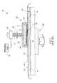
- FIG. 1schematically illustrates a rotary CMP machine 10 with a platen 20 , a carrier assembly 30 , and a planarizing pad 40 .
- the CMP machine 10may also have an under-pad 25 between an upper surface 22 of the platen 20 and a lower surface of the planarizing pad 40 .
- a drive assembly 26rotates the platen 20 (indicated by arrow F) and/or reciprocates the platen 20 back and forth (indicated by arrow G). Since the planarizing pad 40 is attached to the under-pad 25 , the planarizing pad 40 moves with the platen 20 during planarization.
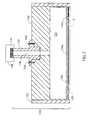
- the carrier assembly 30has a chuck or head 31 with a chamber 32 , a retaining member 33 around a perimeter of the head 31 , and a backing assembly in the chamber 32 .
- the backing assemblyincludes a plate 34 and a diaphragm 35 on the exterior of the plate 34 .
- the plate 34can have a plurality of holes through which air can pass to act against the diaphragm.
- the carrier assembly 30also has a pneumatic line 36 through a shaft 37 , a rotary coupling 38 on the shaft 37 , and an actuator assembly 39 (shown schematically) that rotates the shaft 37 .
- the actuator assembly 39translates or rotates the head 31 (arrows I and J respectively), and the rotary coupling 38 couples a pneumatic pump to the pneumatic line 36 .
- a positive air pressureis applied to the plate 34 by pumping air into the chamber 32 via the pneumatic line 36 , or a vacuum is applied by drawing air from the chamber 32 via the pneumatic line 36 .
- the planarizing pad 40 and a planarizing solution 44define a planarizing medium that mechanically and/or chemically-mechanically removes material from the surface of a micro-device workpiece 12 in the head 31 .
- the planarizing solution 44may be a conventional CMP slurry with abrasive particles and chemicals that etch and/or oxidize the surface of the micro-device workpiece 12 , or the planarizing solution 44 may be a “clean” non-abrasive planarizing solution without abrasive particles.
- abrasive slurries with abrasive particlesare used on non-abrasive polishing pads, and clean non-abrasive solutions without abrasive particles are used on fixed-abrasive polishing pads.
- the carrier assembly 30presses the workpiece 12 face-downward against the planarizing pad 40 . More specifically, the carrier assembly 30 generally presses the micro-device workpiece 12 against the planarizing solution 44 on a planarizing surface 42 of the planarizing pad 40 , and the platen 20 and/or the carrier assembly 30 moves to rub the workpiece 12 against the planarizing surface 42 . As the micro-device workpiece 12 rubs against the planarizing surface 42 , the planarizing medium removes material from the face of the workpiece 12 .
- the CMP processmust consistently and accurately produce a uniformly planar surface on the workpiece 12 to enable precise fabrication of circuits and photo-patterns.
- a non-uniform surfacecan result, for example, when material is removed more quickly in one area than another during CMP processing.
- the carrier head shown in FIG. 1can adjust the downforce by controlling the air pressure in the chamber 32 .
- These carrier headshave several drawbacks. For example, the diaphragm may rip during a planarizing cycle. When this occurs, the planarizing machine is programmed to apply a vacuum in the chamber 32 for holding the workpiece in the head 31 .
- planarizing solution 44This causes the planarizing solution 44 to back-flow into the chamber 32 and up through the pneumatic line 36 to the rotary coupling 38 .
- the planarizing solutionfouls the rotary coupling 38 , the pneumatic line 36 , and the plate 34 .
- the rotary coupling 38may fail because of such fouling, which can cause unnecessary downtime for repairing the head 31 .
- the fouling of the pneumatic line 36 and plate 34may also make it difficult to control the distribution of backside pressure on the workpiece because the planarizing solution can obstruct the pneumatic line 36 or the holes in the plate 34 . This often results in non-uniform surfaces on workpieces.
- a carrier assembly for holding a microelectronic workpiececomprises a head, a backing assembly in the head, and a selective barrier.
- the headincludes a chamber, a pneumatic line in fluid communication with the chamber through which a pneumatic fluid passes, and a retaining member defining a perimeter portion of a workpiece cavity.
- the backing assemblyis positioned in the chamber of the head.
- the backing assemblyfor example, can include a plate in the chamber and a diaphragm on one side of the plate. The diaphragm further defines a backside portion of the workpiece cavity.
- the selective barrieris positioned in at least one of the chamber and/or the pneumatic line, and the barrier is configured to inhibit contaminants from back-flowing into at least a portion of the pneumatic line. As a result, when the diaphragm rips, the barrier prevents the planarizing solution from fouling the pneumatic line and/or the rotary coupling.
- the barriercan be located in the pneumatic line, the chamber, or at the plate.
- the barriercan comprise a material that allows air to pass through the pneumatic line while blocking liquids and solids from proceeding past the barrier.
- the barriercan be a membrane that allows gases to pass through the pneumatic line.
- the barriercan be a filter that removes solid particles from the fluid flow.
- the filterfor example, can be a mesh, random woven strands, a porous pad, or other type of porous material that prevents abrasive particles and other particulates in the planarizing solution from flowing past the filter.
- Certain embodiments of filterscan allow liquid and air to flow through the pneumatic line. Suitable materials for the filter include nylon, ceramics, polyesters, compressed materials, sintered materials, nano-tubes, and other materials.
- a carrier assembly for holding a microelectronic workpieceincludes a head having a retaining member and a backing member positioned with respect to the retaining member to define a workpiece cavity for retaining the workpiece.
- the carrier assemblycan also include a pneumatic assembly having a pneumatic line to transport a flow of gas relative to the backing member and a selective barrier in the pneumatic assembly that inhibits liquids and/or solids from back-flowing through at least a portion of the pneumatic line.
- the carrier assemblycan further comprise a chamber in the head, and the backing member can be positioned to enclose a portion of the chamber.
- the selective barriercan be located in the pneumatic line and/or the chamber, and the selective barrier can be a membrane, a filter, or another material.
- the selective barriercan be configured to allow air to pass through the pneumatic line, but prevent liquids and particulate matter from passing beyond the membrane.
- Still additional embodimentsare directed towards planarizing machines that have a table, a planarizing pad on the table, and a carrier assembly for holding a microelectronic workpiece as set forth above.
- These planarizing machinescan be used to planarize a microelectronic workpiece by holding the workpiece in the head so that the backside of the workpiece contacts the diaphragm.
- the methodcontinues by covering a portion of the planarizing surface of the polishing pad with a planarizing solution and then pressing the workpiece against the planarizing surface by providing a pressure against the workpiece via the pneumatic line and the diaphragm.
- the methodcan further include filtering liquids and/or solids on the backside of the diaphragm to inhibit or completely prevent them from flowing into the pneumatic line during a planarizing cycle.
- FIG. 1is a schematic diagram of a rotary planarizing machine having a carrier assembly in accordance with the prior art.
- FIG. 2is a schematic illustration of a planarizing machine in accordance with an embodiment of the invention.
- FIG. 3is a cross-sectional view of a carrier assembly for use in a planarizing machine in accordance with one embodiment of the invention.
- FIG. 4is a cross-sectional view of a carrier assembly for use in a planarizing machine in accordance with another embodiment of the invention.
- FIG. 5is a cross-sectional view of a carrier assembly for use in a planarizing machine in accordance with another embodiment of the invention.
- FIG. 6is a cross-sectional view of a carrier assembly for use in a planarizing machine in accordance with another embodiment of the invention.
- FIG. 7is a cross-sectional view of a carrier assembly for use in a planarizing machine in accordance with another embodiment of the invention.
- the present inventionis directed toward carrier assemblies, planarizing machines with carrier assemblies, and methods for mechanical and/or chemical-mechanical planarization of micro-device workpieces.
- micro-device workpieceincludes micro-mechanical and microelectronic workpieces, such as semiconductor wafers, field emission displays, and read-write heads.
- FIGS. 2-7Several embodiments of the invention are described below with reference to FIGS. 2-7 , but it will be appreciated that the invention can include other embodiments not shown in FIGS. 2-7 .
- aspects of the inventioncan include embodiments that do not have all of the features disclosed in FIGS. 2-7 , or other embodiments can include features in addition to those disclosed in FIGS. 2-7 .
- the embodiments disclosed in FIGS. 2-7are directed toward both rotary planarizing machines and web-format planarizing machines even though the following description focuses on rotary planarizing machines.
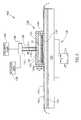
- FIG. 2is a schematic illustration showing a planarizing machine 100 including a carrier assembly 130 in accordance with an embodiment of the invention.
- the planarizing machine 100also includes a table 120 that is driven by a table actuator 126 .
- the table 120can be a rotary platen that rotates or reciprocates as shown by arrows F and G, or it can be a fixed table.
- a polishing pad 140 having a planarizing surface 142is attached to the table 120 .
- the polishing pad 140can be a non-abrasive pad or a fixed abrasive pad as described above.
- a planarizing solution 144is deposited over the planarizing surface 142 .
- the carrier assembly 130carries the workpiece 12 during the planarizing cycle.
- the carrier assembly 130can rotate and/or translate the workpiece 12 across the planarizing surface 142 .
- the carrier assemblyincludes a chuck or head 131 that has a chamber 132 .
- the carrier assembly 130also includes a retaining member 133 , such as a retaining ring, that extends around at least a portion of the head 131 .
- the retaining member 133generally encircles the head 131 , and it can move vertically with respect to the head 131 as shown by arrow V.
- the carrier assembly 130also includes a backing assembly in the head 131 .
- the backing assemblycan include a diaphragm 135 that encloses the chamber 132 .
- the retaining member 133 and the diaphragm 135define a workpiece cavity in which the workpiece 12 is retained for loading and unloading during a planarizing cycle.
- the backing assemblycan further include a back-plate 134 on the backside of the diaphragm 135 .
- the back-plate 134is generally a flexible plate with openings 134 a .
- the back-plate 134can be a lightweight material, and the openings 134 a can be arranged in different patterns to allow air to flow through the back-plate 134 and act against the diaphragm 135 .
- the back-plate 134also can move up or down within the chamber 132 .
- the carrier assembly 130also includes a pneumatic assembly that is carried by the head 131 .
- the pneumatic assemblyprovides a positive pneumatic pressure to the back-plate 134 and the diaphragm 135 for adjusting the downforce against the workpiece 12 , or the pneumatic assembly provides a suction that draws the diaphragm 135 into the openings 134 a in the back-plate 134 for holding the workpiece 12 in the head 131 .
- the pneumatic assemblyincludes a pneumatic line 136 in a shaft 137 , a rotary coupling 138 , and a pneumatic pump 150 coupled to the line 136 via the rotary coupling 138 . The pneumatic assembly accordingly transports a gas flow through the head 131 relative to the backing assembly.
- the carrier assembly 130can further include a selective barrier 170 in the pneumatic assembly that inhibits contaminants, such as slurry particles and/or liquids, from back-flowing through at least a portion of the pneumatic line 136 .
- the selective barrier 170can be a filter or a membrane that is configured to prevent liquids and/or solid particles from back-flowing through the pneumatic line 136 and the rotary coupling 138 .
- One suitable selective barrierallows air or other gases to pass through the pneumatic line 136 , but prevents or at least inhibits liquids and solids from passing through the pneumatic line 136 .
- Suitable selective barriersallow gases and liquids to pass through the pneumatic line 136 , but generally inhibit solids from fouling the line 136 and the rotary coupling 138 .
- the selective barrier 170can become clogged with particles to the extent that it also blocks liquids from back-flowing through the pneumatic system.
- Suitable selective barriersinclude filters or membranes made from nylon, ceramics, polyesters, sintered materials, carbon (e.g., pressed blocks or nano-tube structures), and other materials. It is expected that organic, hydrophilic membranes will work well for the barrier member.
- nylon membranesare hydrophilic, strong, dimensionally stable, and easy to fabricate.
- Nylon membranesare also corrosion resistant, stable up to 180° C., and stable in high pH environments.
- One suitable materialis a nylon mesh manufactured by Spectrum Laboratories under part number 145799, but many other materials can be used for the selective barrier.
- the selective barrier 170can be between the head 131 and the shaft 137 .
- the selective barrier 170is at a distal end of the shaft 137 to protect the pneumatic line 136 from being fouled by planarizing solution when the diaphragm 135 ruptures.
- the selective barrier 170is preferably positioned within the head 131 to be close to the chamber 132 .
- the barrier assembly 170can also be positioned in the chamber 132 at the distal end of the pneumatic line 136 in other embodiments. Such positioning of the selective barrier 170 accordingly provides the most protection against the back-flow of planarizing solution through the pneumatic assembly.
- the barrier 170can be located in the line 136 or other parts of the carrier assembly 130 .
- the carrier assembly 130 shown in FIG. 2operates to protect the pneumatic line 136 and the rotary coupling 138 from being fouled by planarizing solution when the diaphragm 135 tears or is otherwise damaged during a planarizing cycle.
- typical planarizing machinesprovide a positive pneumatic pressure in the chamber 132 during a planarizing cycle, but reverse the positive pressure to create a vacuum in the chamber 132 when the diaphragm tears to avoid damaging the workpiece 12 . Accordingly, the vacuum in the chamber 132 draws planarizing solution through the damaged portion of the diaphragm 135 and into the chamber 132 .
- the selective barrier 170allows air or other gases to pass through pneumatic line 136 , but the selective barrier 170 prevents or otherwise inhibits planarizing solution from passing beyond the selective barrier 170 .
- the planarizing machine 100can continue to draw a vacuum against the backside of the workpiece 12 after the diaphragm 135 has been damaged, but it protects the pneumatic line 136 and the rotary coupling 138 from being fouled by the planarizing solution 144 . Therefore, the particular embodiment of the carrier assembly 130 illustrated in FIG. 2 is expected to reduce the downtime and non-uniformities that can occur when the diaphragm 135 tears.
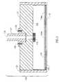
- FIG. 3is a cross-sectional view of a carrier assembly 130 illustrating an embodiment of the selective barrier 170 in greater detail.
- the selective barrier 170is removable to provide quick, easy cleaning of the carrier head 131 if the diaphragm 135 ruptures.
- the shaft 137is coupled to the head 131 by a plurality of fasteners 152 , such as bolts.
- the selective barrier 170can be an annular filter or membrane that is clamped between the shaft 137 and the head 131 when the fasteners 152 are secured to the head 131 .
- the selective barrier 170can be replaced each time after the diaphragm 135 is damaged by simply removing the fasteners 152 to disconnect the shaft 137 from the head 131 .
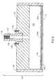
- FIGS. 4-7illustrate additional embodiments of carrier heads 130 in accordance with the invention.
- the selective barrier 170can be positioned directly in the distal portion of the pneumatic line 136 .
- the selective barrier 170 shown in FIG. 4further protects the pneumatic line 136 by being closer to the chamber 132 compared to the embodiment shown in FIGS. 2 and 3 .
- the selective barrier 170 shown in FIG. 4can have a flange 171 that is clamped between the distal end of the shaft 137 and the head 131 .
- FIG. 5illustrates another embodiment in which the selective barrier 170 is positioned in the chamber 132 at the distal end of the pneumatic line 136 .
- FIG. 5further protects the pneumatic line 136 because it inhibits fluids and/or solids from even entering the pneumatic line 136 .
- FIG. 6illustrates another embodiment in which the selective barrier 170 is positioned in the pneumatic line 136 along the shaft 137 .
- FIG. 7illustrates another embodiment in which the selective barrier 170 is positioned on a proximal end of the shaft 137 adjacent to the rotary coupling 138 .
- the embodiments shown in FIGS. 6 and 7protect the rotary coupling 138 , but they do not protect the pneumatic line 136 .
- the embodiments of the carrier assembly 130 shown in FIGS. 4-7are expected to operate in substantially the same manner as the embodiment shown in FIG. 2 .
Landscapes
- Engineering & Computer Science (AREA)
- Mechanical Engineering (AREA)
- Mechanical Treatment Of Semiconductor (AREA)
- Finish Polishing, Edge Sharpening, And Grinding By Specific Grinding Devices (AREA)
Abstract
Description
The present invention relates to carrier assemblies, planarizing machines with carrier assemblies, and methods for mechanical and/or chemical-mechanical planarization of micro-device workpieces.
Mechanical and chemical-mechanical planarization processes (collectively “CMP”) remove material from the surface of micro-device workpieces in the production of microelectronic devices and other products.FIG. 1 schematically illustrates arotary CMP machine 10 with a platen20, acarrier assembly 30, and a planarizingpad 40. TheCMP machine 10 may also have an under-pad 25 between anupper surface 22 of the platen20 and a lower surface of the planarizingpad 40. Adrive assembly 26 rotates the platen20 (indicated by arrow F) and/or reciprocates the platen20 back and forth (indicated by arrow G). Since theplanarizing pad 40 is attached to the under-pad 25, theplanarizing pad 40 moves with the platen20 during planarization.
Thecarrier assembly 30 has a chuck orhead 31 with achamber 32, aretaining member 33 around a perimeter of thehead 31, and a backing assembly in thechamber 32. The backing assembly includes aplate 34 and adiaphragm 35 on the exterior of theplate 34. Theplate 34 can have a plurality of holes through which air can pass to act against the diaphragm. Thecarrier assembly 30 also has apneumatic line 36 through ashaft 37, arotary coupling 38 on theshaft 37, and an actuator assembly39 (shown schematically) that rotates theshaft 37. Theactuator assembly 39 translates or rotates the head31 (arrows I and J respectively), and therotary coupling 38 couples a pneumatic pump to thepneumatic line 36. In operation, a positive air pressure is applied to theplate 34 by pumping air into thechamber 32 via thepneumatic line 36, or a vacuum is applied by drawing air from thechamber 32 via thepneumatic line 36.
Theplanarizing pad 40 and a planarizingsolution 44 define a planarizing medium that mechanically and/or chemically-mechanically removes material from the surface of amicro-device workpiece 12 in thehead 31. The planarizingsolution 44 may be a conventional CMP slurry with abrasive particles and chemicals that etch and/or oxidize the surface of themicro-device workpiece 12, or the planarizingsolution 44 may be a “clean” non-abrasive planarizing solution without abrasive particles. In most CMP applications, abrasive slurries with abrasive particles are used on non-abrasive polishing pads, and clean non-abrasive solutions without abrasive particles are used on fixed-abrasive polishing pads.
To planarize themicro-device workpiece 12 with theCMP machine 10, thecarrier assembly 30 presses theworkpiece 12 face-downward against the planarizingpad 40. More specifically, thecarrier assembly 30 generally presses themicro-device workpiece 12 against the planarizingsolution 44 on a planarizingsurface 42 of theplanarizing pad 40, and the platen20 and/or thecarrier assembly 30 moves to rub theworkpiece 12 against the planarizingsurface 42. As themicro-device workpiece 12 rubs against the planarizingsurface 42, the planarizing medium removes material from the face of theworkpiece 12.
The CMP process must consistently and accurately produce a uniformly planar surface on theworkpiece 12 to enable precise fabrication of circuits and photo-patterns. A non-uniform surface can result, for example, when material is removed more quickly in one area than another during CMP processing. To compensate for the non-uniform removal of material, the carrier head shown inFIG. 1 can adjust the downforce by controlling the air pressure in thechamber 32. These carrier heads, however, have several drawbacks. For example, the diaphragm may rip during a planarizing cycle. When this occurs, the planarizing machine is programmed to apply a vacuum in thechamber 32 for holding the workpiece in thehead 31. This causes the planarizingsolution 44 to back-flow into thechamber 32 and up through thepneumatic line 36 to therotary coupling 38. The planarizing solution fouls therotary coupling 38, thepneumatic line 36, and theplate 34. Therotary coupling 38 may fail because of such fouling, which can cause unnecessary downtime for repairing thehead 31. The fouling of thepneumatic line 36 andplate 34 may also make it difficult to control the distribution of backside pressure on the workpiece because the planarizing solution can obstruct thepneumatic line 36 or the holes in theplate 34. This often results in non-uniform surfaces on workpieces.
The present invention is directed toward carrier assemblies, planarizing machines with carrier assemblies, and methods for mechanical and/or chemical-mechanical planarization of micro-device workpieces. In one embodiment, a carrier assembly for holding a microelectronic workpiece comprises a head, a backing assembly in the head, and a selective barrier. The head includes a chamber, a pneumatic line in fluid communication with the chamber through which a pneumatic fluid passes, and a retaining member defining a perimeter portion of a workpiece cavity. The backing assembly is positioned in the chamber of the head. The backing assembly, for example, can include a plate in the chamber and a diaphragm on one side of the plate. The diaphragm further defines a backside portion of the workpiece cavity. The selective barrier is positioned in at least one of the chamber and/or the pneumatic line, and the barrier is configured to inhibit contaminants from back-flowing into at least a portion of the pneumatic line. As a result, when the diaphragm rips, the barrier prevents the planarizing solution from fouling the pneumatic line and/or the rotary coupling.
The barrier can be located in the pneumatic line, the chamber, or at the plate. The barrier can comprise a material that allows air to pass through the pneumatic line while blocking liquids and solids from proceeding past the barrier. For example, in one embodiment the barrier can be a membrane that allows gases to pass through the pneumatic line. In other embodiments, the barrier can be a filter that removes solid particles from the fluid flow. The filter, for example, can be a mesh, random woven strands, a porous pad, or other type of porous material that prevents abrasive particles and other particulates in the planarizing solution from flowing past the filter. Certain embodiments of filters can allow liquid and air to flow through the pneumatic line. Suitable materials for the filter include nylon, ceramics, polyesters, compressed materials, sintered materials, nano-tubes, and other materials.
Another embodiment of a carrier assembly for holding a microelectronic workpiece includes a head having a retaining member and a backing member positioned with respect to the retaining member to define a workpiece cavity for retaining the workpiece. The carrier assembly can also include a pneumatic assembly having a pneumatic line to transport a flow of gas relative to the backing member and a selective barrier in the pneumatic assembly that inhibits liquids and/or solids from back-flowing through at least a portion of the pneumatic line. In this embodiment, the carrier assembly can further comprise a chamber in the head, and the backing member can be positioned to enclose a portion of the chamber. The selective barrier can be located in the pneumatic line and/or the chamber, and the selective barrier can be a membrane, a filter, or another material. The selective barrier can be configured to allow air to pass through the pneumatic line, but prevent liquids and particulate matter from passing beyond the membrane.
Still additional embodiments are directed towards planarizing machines that have a table, a planarizing pad on the table, and a carrier assembly for holding a microelectronic workpiece as set forth above. These planarizing machines can be used to planarize a microelectronic workpiece by holding the workpiece in the head so that the backside of the workpiece contacts the diaphragm. The method continues by covering a portion of the planarizing surface of the polishing pad with a planarizing solution and then pressing the workpiece against the planarizing surface by providing a pressure against the workpiece via the pneumatic line and the diaphragm. The method can further include filtering liquids and/or solids on the backside of the diaphragm to inhibit or completely prevent them from flowing into the pneumatic line during a planarizing cycle.
The present invention is directed toward carrier assemblies, planarizing machines with carrier assemblies, and methods for mechanical and/or chemical-mechanical planarization of micro-device workpieces. As used herein, the term “micro-device workpiece” includes micro-mechanical and microelectronic workpieces, such as semiconductor wafers, field emission displays, and read-write heads. Several embodiments of the invention are described below with reference toFIGS. 2-7 , but it will be appreciated that the invention can include other embodiments not shown inFIGS. 2-7 . For example, aspects of the invention can include embodiments that do not have all of the features disclosed inFIGS. 2-7 , or other embodiments can include features in addition to those disclosed inFIGS. 2-7 . Additionally, the embodiments disclosed inFIGS. 2-7 are directed toward both rotary planarizing machines and web-format planarizing machines even though the following description focuses on rotary planarizing machines.
Thecarrier assembly 130 carries theworkpiece 12 during the planarizing cycle. Thecarrier assembly 130, for example, can rotate and/or translate theworkpiece 12 across theplanarizing surface 142. In this embodiment, the carrier assembly includes a chuck orhead 131 that has achamber 132. Thecarrier assembly 130 also includes a retainingmember 133, such as a retaining ring, that extends around at least a portion of thehead 131. The retainingmember 133 generally encircles thehead 131, and it can move vertically with respect to thehead 131 as shown by arrow V. Thecarrier assembly 130 also includes a backing assembly in thehead 131. The backing assembly can include adiaphragm 135 that encloses thechamber 132. The retainingmember 133 and thediaphragm 135 define a workpiece cavity in which theworkpiece 12 is retained for loading and unloading during a planarizing cycle. In other embodiments, the backing assembly can further include a back-plate 134 on the backside of thediaphragm 135. The back-plate 134 is generally a flexible plate withopenings 134a. The back-plate 134, for example, can be a lightweight material, and theopenings 134acan be arranged in different patterns to allow air to flow through the back-plate 134 and act against thediaphragm 135. The back-plate 134 also can move up or down within thechamber 132.
Thecarrier assembly 130 also includes a pneumatic assembly that is carried by thehead 131. The pneumatic assembly provides a positive pneumatic pressure to the back-plate 134 and thediaphragm 135 for adjusting the downforce against theworkpiece 12, or the pneumatic assembly provides a suction that draws thediaphragm 135 into theopenings 134ain the back-plate 134 for holding theworkpiece 12 in thehead 131. In this embodiment, the pneumatic assembly includes apneumatic line 136 in ashaft 137, arotary coupling 138, and apneumatic pump 150 coupled to theline 136 via therotary coupling 138. The pneumatic assembly accordingly transports a gas flow through thehead 131 relative to the backing assembly.
Thecarrier assembly 130 can further include aselective barrier 170 in the pneumatic assembly that inhibits contaminants, such as slurry particles and/or liquids, from back-flowing through at least a portion of thepneumatic line 136. Theselective barrier 170, for example, can be a filter or a membrane that is configured to prevent liquids and/or solid particles from back-flowing through thepneumatic line 136 and therotary coupling 138. One suitable selective barrier allows air or other gases to pass through thepneumatic line 136, but prevents or at least inhibits liquids and solids from passing through thepneumatic line 136. Other suitable selective barriers allow gases and liquids to pass through thepneumatic line 136, but generally inhibit solids from fouling theline 136 and therotary coupling 138. Theselective barrier 170 can become clogged with particles to the extent that it also blocks liquids from back-flowing through the pneumatic system. Suitable selective barriers include filters or membranes made from nylon, ceramics, polyesters, sintered materials, carbon (e.g., pressed blocks or nano-tube structures), and other materials. It is expected that organic, hydrophilic membranes will work well for the barrier member. For example, nylon membranes are hydrophilic, strong, dimensionally stable, and easy to fabricate. Nylon membranes are also corrosion resistant, stable up to 180° C., and stable in high pH environments. One suitable material is a nylon mesh manufactured by Spectrum Laboratories under part number 145799, but many other materials can be used for the selective barrier.
As shown inFIG. 2 , theselective barrier 170 can be between thehead 131 and theshaft 137. In this embodiment, theselective barrier 170 is at a distal end of theshaft 137 to protect thepneumatic line 136 from being fouled by planarizing solution when thediaphragm 135 ruptures. Theselective barrier 170 is preferably positioned within thehead 131 to be close to thechamber 132. Thebarrier assembly 170 can also be positioned in thechamber 132 at the distal end of thepneumatic line 136 in other embodiments. Such positioning of theselective barrier 170 accordingly provides the most protection against the back-flow of planarizing solution through the pneumatic assembly. As explained below, however, thebarrier 170 can be located in theline 136 or other parts of thecarrier assembly 130.
Thecarrier assembly 130 shown inFIG. 2 operates to protect thepneumatic line 136 and therotary coupling 138 from being fouled by planarizing solution when thediaphragm 135 tears or is otherwise damaged during a planarizing cycle. For example, typical planarizing machines provide a positive pneumatic pressure in thechamber 132 during a planarizing cycle, but reverse the positive pressure to create a vacuum in thechamber 132 when the diaphragm tears to avoid damaging theworkpiece 12. Accordingly, the vacuum in thechamber 132 draws planarizing solution through the damaged portion of thediaphragm 135 and into thechamber 132. Theselective barrier 170 allows air or other gases to pass throughpneumatic line 136, but theselective barrier 170 prevents or otherwise inhibits planarizing solution from passing beyond theselective barrier 170. As a result, theplanarizing machine 100 can continue to draw a vacuum against the backside of theworkpiece 12 after thediaphragm 135 has been damaged, but it protects thepneumatic line 136 and therotary coupling 138 from being fouled by theplanarizing solution 144. Therefore, the particular embodiment of thecarrier assembly 130 illustrated inFIG. 2 is expected to reduce the downtime and non-uniformities that can occur when thediaphragm 135 tears.
From the foregoing, it will be appreciated that specific embodiments of the invention have been described herein for purposes of illustration, but that various modifications may be made without deviating from the spirit and scope of the invention. Accordingly, the invention is not limited except as by the appended claims.
Claims (58)
1. A carrier assembly for holding a microelectronic workpiece in a mechanical or chemical-mechanical planarization machine, comprising:
a head including a chamber, a pneumatic line in fluid communication with the chamber through which a pneumatic flow passes, and a retaining member defining a perimeter of portion of a workpiece cavity;
a backing assembly in the head having a plate in the chamber and a diaphragm on one side of the plate, the diaphragm defining a backside portion of the workpiece cavity; and
a filter in at least one of the chamber and the pneumatic line, the filter being configured to inhibit contaminants from back-flowing into at least a portion of the pneumatic line.
2. The carrier assembly ofclaim 1 wherein the filter is located in the pneumatic line.
3. The carrier assembly ofclaim 1 wherein the filter is located in the chamber.
4. The carrier assembly ofclaim 1 wherein the filter comprises a material that allows air to pass through the pneumatic line and blocks fluid from passing through the pneumatic line.
5. The carrier assembly ofclaim 1 wherein the filter comprises a nylon mesh.
6. The carrier assembly ofclaim 1 wherein the plate moves within the chamber and the plate has holes through which the pneumatic flow can exert a force against the diaphragm.
7. A carrier assembly for holding a microelectronic workpiece in a planarization machine, comprising:
a head including a retaining member that defines a perimeter portion of a workpiece cavity for containing a workpiece;
a backing assembly in the head, the backing assembly having a diaphragm within the retaining member to define a backside portion of the workpiece cavity;
a pneumatic assembly carried by the head, the pneumatic assembly having a pneumatic line to transport a gas flow through the head relative to the backing assembly; and
a filter in the head at a location through which the gas flow passes.
8. The carrier assembly ofclaim 7 , further comprising a chamber in the head and a back-plate in the chamber, and wherein the pneumatic line transports the gas flow to/from the chamber.
9. The carrier assembly ofclaim 8 wherein the filter is located in the pneumatic line.
10. The carrier assembly ofclaim 8 wherein the filter is located in the chamber.
11. The carrier assembly ofclaim 8 wherein the filter comprises a material that allows air to pass through the pneumatic line and blocks fluid from passing through the pneumatic line.
12. The carrier assembly ofclaim 8 wherein the filter comprises a nylon mesh.
13. The carrier assembly ofclaim 8 wherein the back-plate moves within the chamber and the back-plate has holes through which the pneumatic flow can exert a force against the diaphragm.
14. A carrier assembly for holding a microelectronic workpiece in a planarization machine, comprising:
a head having a retaining member and a backing member positioned with respect to the retaining member to define a workpiece cavity for retaining the workpiece;
a pneumatic assembly having a pneumatic line to transport a flow of gas relative to the backing member; and
a selective barrier in the pneumatic assembly that at least inhibits mailer from back-flowing through at least a portion of the pneumatic line.
15. The carrier assembly ofclaim 14 , further comprising a chamber in the head, wherein the backing member encloses a portion of the chamber, and wherein the pneumatic line transports the gas flow to/from the chamber.
16. The carrier assembly ofclaim 15 wherein the selective barrier is located in the pneumatic line.
17. The carrier assembly ofclaim 15 wherein the selective barrier is located in the chamber.
18. The carrier assembly ofclaim 15 wherein the selective barrier comprises a membrane that allows air to pass through the pneumatic line and inhibits fluid from passing through the pneumatic line.
19. The carrier assembly ofclaim 15 wherein the selective barrier is a filter.
20. The carrier assembly ofclaim 15 wherein the selective barrier comprises a nylon mesh.
21. The carrier assembly ofclaim 15 wherein the backing member comprises a plate that moves within the chamber and a diaphragm on an exterior side of the plate, and wherein the plate has holes through which the pneumatic flow can exert a force against the diaphragm.
22. A carrier assembly for holding a microelectronic workpiece in a planarization machine, comprising:
a head having a backing assembly with a diaphragm configured to contact a backside of a workpiece;
a pneumatic control assembly carried by the head, the pneumatic control assembly having a pneumatic line configured to transport a gas flow relative to the backing assembly; and
a barrier means in the pressure control assembly that inhibit contaminants which have passed through an opening in the diaphragm from back-flowing through at least a portion of the pressure control assembly.
23. The carrier assembly ofclaim 22 , further comprising a backside chamber in the head, wherein the diaphragm encloses a portion of the backside chamber and wherein the pneumatic line transports the gas flow to/from the backside chamber.
24. The carrier assembly ofclaim 23 wherein the barrier means is located in the pneumatic line.
25. The carrier assembly ofclaim 23 wherein the barrier means is located in the chamber.
26. The carrier assembly ofclaim 23 wherein the barrier means comprises a membrane that allows air to pass through the pneumatic line and blocks fluid from passing through the pneumatic line.
27. The carrier assembly ofclaim 23 wherein the barrier means comprises a filter.
28. The carrier assembly ofclaim 23 wherein the barrier means comprises nylon mesh.
29. The carrier assembly ofclaim 23 wherein the backing assembly further comprises a plate that moves within the chamber, and wherein the plate has holes through which the pneumatic flow can exert a force against the diaphragm.
30. A planarizing machine for mechanical and/or chemical-mechanical planarization of a workpiece, comprising:
a table;
a planarizing pad on the table;
a carrier assembly for holding a microelectronic workpiece, the carrier assembly comprising
a head including a backside chamber, a pneumatic line in fluid communication with the chamber through which a pneumatic flow passes, and a retaining member defining a perimeter of portion of a workpiece cavity;
a backing assembly in the head having a plate in the chamber and a diaphragm on one side of the plate, the diaphragm defining a backside portion of the workpiece cavity; and
a filter in at least one of the chamber and the pneumatic line, the filter being configured to inhibit contaminants from back-flowing into at least a portion of the pneumatic line.
31. The planarizing machine ofclaim 30 wherein the filter is located in the pneumatic line.
32. The planarizing machine ofclaim 30 wherein the filter is located in the chamber.
33. The planarizing machine ofclaim 30 wherein the filter comprises a material that allows air to pass through the pneumatic line and blocks fluid from passing through the pneumatic line.
34. The planarizing machine ofclaim 30 wherein the filter comprises a nylon mesh.
35. The planarizing machine ofclaim 30 wherein the plate moves within the chamber and the plate has holes through which the pneumatic flow can exert a force against the diaphragm.
36. A planarizing machine for mechanical and/or chemical-mechanical planarization of a workpiece, comprising:
a table;
a planarizing pad on the table;
a carrier assembly for holding a microelectronic workpiece, the carrier assembly including
a head including a retaining member that defines a perimeter portion of a workpiece cavity for containing a workpiece;
a backing assembly in the head, the backing assembly having a back-plate and a diaphragm, the diaphragm being within the retaining member and on one side of the plate to define a backside portion of the workpiece cavity;
a pneumatic assembly carried by the head, the pneumatic assembly having a pneumatic line to transport a gas flow through the head relative to the backing assembly; and
a filter in the head at a location through which the gas flow passes.
37. The carrier assembly ofclaim 36 , further comprising a chamber in the head and a back-plate in the chamber, and wherein the pneumatic line transports the gas flow to/from the chamber.
38. The carrier assembly ofclaim 37 wherein the filter is located in the pneumatic line.
39. The carrier assembly ofclaim 37 wherein the filter is located in the chamber.
40. The carrier assembly ofclaim 37 wherein the filter comprises a material that allows air to pass through the pneumatic line and blocks fluid from passing through the pneumatic line.
41. The carrier assembly ofclaim 37 wherein the filter comprises a nylon mesh.
42. The carrier assembly ofclaim 37 wherein the back-plate moves within the chamber and the back-plate has holes through which the pneumatic flow can exert a force against the diaphragm.
43. A planarizing machine for mechanical and/or chemical-mechanical planarization of a workpiece, comprising:
a table;
a planarizing pad on the table;
a carrier assembly for holding a microelectronic workpiece, the carrier assembly comprising
a head having a retaining member and a backing member positioned with respect to the retaining member to define a workpiece cavity for retaining the workpiece;
a pneumatic assembly having a pneumatic line to transport a flow of gas relative to the backing member; and
a selective barrier in the pneumatic assembly that at least inhibits matter from back-flowing through at least a portion of the pneumatic line.
44. The carrier assembly ofclaim 43 , further comprising a chamber in the heads wherein the backing member encloses a portion of the chamber, and wherein the pneumatic line transports the gas flow to/from the chamber.
45. The carrier assembly ofclaim 44 wherein the selective barrier is located in the pneumatic line.
46. The carrier assembly ofclaim 44 wherein the selective barrier is located in the chamber.
47. The carrier assembly ofclaim 44 wherein the selective barrier comprises a membrane that allows air to pass through the pneumatic line and inhibits fluid from passing through the pneumatic line.
48. The carrier assembly ofclaim 44 wherein the selective barrier comprises a filter.
49. The carrier assembly ofclaim 44 wherein the selective barrier comprises a nylon mesh.
50. The carrier assembly ofclaim 44 wherein the backing member comprises a plate that moves within the chamber and a diaphragm on an exterior side of the plate, and wherein the plate has holes through which the pneumatic flow can exert a force against the diaphragm.
51. A planarizing machine for mechanical and/or chemical-mechanical planarization of a workpiece, comprising:
a table;
a planarizing pad on the table;
a carrier assembly for holding a microelectronic workpiece, the carrier assembly comprising
a head having a backing assembly with a diaphragm configured to contact a backside of a workpiece;
a pneumatic control assembly carried by the head, the pneumatic control assembly having a pneumatic line configured to transport a gas flow relative to the backing assembly; and
a selective barrier in the pressure control assembly to inhibit contaminants from back-flowing through at least a portion of the pressure control assembly.
52. The carrier assembly ofclaim 51 , further comprising a backside chamber in the head, wherein the diaphragm encloses a portion of the backside chamber, and wherein the pneumatic line transports the gas flow to/from the backside chamber.
53. The carrier assembly ofclaim 52 wherein the selective barrier is located in the pneumatic line.
54. The carrier assembly ofclaim 52 wherein the selective barrier is located in the chamber.
55. The carrier assembly ofclaim 52 wherein the selective barrier comprises a membrane that allows air to pass through the pneumatic line and inhibits fluid from passing through the pneumatic line.
56. The carrier assembly ofclaim 52 wherein the selective barrier comprises a filter.
57. The carrier assembly ofclaim 52 wherein the selective barrier comprises a nylon mesh.
58. The carrier assembly ofclaim 52 wherein the backing assembly further comprises a plate that moves within the chamber, and wherein the plate has holes through which the pneumatic flow can exert a force against the diaphragm.
Priority Applications (2)
| Application Number | Priority Date | Filing Date | Title |
|---|---|---|---|
| US10/215,512US6860798B2 (en) | 2002-08-08 | 2002-08-08 | Carrier assemblies, planarizing apparatuses including carrier assemblies, and methods for planarizing micro-device workpieces |
| US10/929,509US6893332B2 (en) | 2002-08-08 | 2004-08-30 | Carrier assemblies, planarizing apparatuses including carrier assemblies, and methods for planarizing micro-device workpieces |
Applications Claiming Priority (1)
| Application Number | Priority Date | Filing Date | Title |
|---|---|---|---|
| US10/215,512US6860798B2 (en) | 2002-08-08 | 2002-08-08 | Carrier assemblies, planarizing apparatuses including carrier assemblies, and methods for planarizing micro-device workpieces |
Related Child Applications (1)
| Application Number | Title | Priority Date | Filing Date |
|---|---|---|---|
| US10/929,509DivisionUS6893332B2 (en) | 2002-08-08 | 2004-08-30 | Carrier assemblies, planarizing apparatuses including carrier assemblies, and methods for planarizing micro-device workpieces |
Publications (2)
| Publication Number | Publication Date |
|---|---|
| US20040029502A1 US20040029502A1 (en) | 2004-02-12 |
| US6860798B2true US6860798B2 (en) | 2005-03-01 |
Family
ID=31494884
Family Applications (2)
| Application Number | Title | Priority Date | Filing Date |
|---|---|---|---|
| US10/215,512Expired - Fee RelatedUS6860798B2 (en) | 2002-08-08 | 2002-08-08 | Carrier assemblies, planarizing apparatuses including carrier assemblies, and methods for planarizing micro-device workpieces |
| US10/929,509Expired - Fee RelatedUS6893332B2 (en) | 2002-08-08 | 2004-08-30 | Carrier assemblies, planarizing apparatuses including carrier assemblies, and methods for planarizing micro-device workpieces |
Family Applications After (1)
| Application Number | Title | Priority Date | Filing Date |
|---|---|---|---|
| US10/929,509Expired - Fee RelatedUS6893332B2 (en) | 2002-08-08 | 2004-08-30 | Carrier assemblies, planarizing apparatuses including carrier assemblies, and methods for planarizing micro-device workpieces |
Country Status (1)
| Country | Link |
|---|---|
| US (2) | US6860798B2 (en) |
Cited By (1)
| Publication number | Priority date | Publication date | Assignee | Title |
|---|---|---|---|---|
| US20110269378A1 (en)* | 2010-04-30 | 2011-11-03 | K. C. Tech Co., Ltd. | Chemical mechanical polishing system |
Families Citing this family (27)
| Publication number | Priority date | Publication date | Assignee | Title |
|---|---|---|---|---|
| US6623329B1 (en)* | 2000-08-31 | 2003-09-23 | Micron Technology, Inc. | Method and apparatus for supporting a microelectronic substrate relative to a planarization pad |
| US20070049184A1 (en)* | 2005-08-24 | 2007-03-01 | International Business Machines Corporation | Retaining ring structure for enhanced removal rate during fixed abrasive chemical mechanical polishing |
| TW200729374A (en)* | 2006-01-26 | 2007-08-01 | Horng Terng Automation Co Ltd | Method of testing semiconductor device under stable pressure and apparatus for test the same under stable pressure |
| US7731572B2 (en)* | 2007-05-24 | 2010-06-08 | United Microelectronics Corp. | CMP head |
| US8758088B2 (en) | 2011-10-06 | 2014-06-24 | Wayne O. Duescher | Floating abrading platen configuration |
| US8740668B2 (en)* | 2010-03-12 | 2014-06-03 | Wayne O. Duescher | Three-point spindle-supported floating abrasive platen |
| US8602842B2 (en)* | 2010-03-12 | 2013-12-10 | Wayne O. Duescher | Three-point fixed-spindle floating-platen abrasive system |
| US8500515B2 (en) | 2010-03-12 | 2013-08-06 | Wayne O. Duescher | Fixed-spindle and floating-platen abrasive system using spherical mounts |
| US8696405B2 (en) | 2010-03-12 | 2014-04-15 | Wayne O. Duescher | Pivot-balanced floating platen lapping machine |
| US8647170B2 (en) | 2011-10-06 | 2014-02-11 | Wayne O. Duescher | Laser alignment apparatus for rotary spindles |
| US8647172B2 (en) | 2010-03-12 | 2014-02-11 | Wayne O. Duescher | Wafer pads for fixed-spindle floating-platen lapping |
| US8641476B2 (en) | 2011-10-06 | 2014-02-04 | Wayne O. Duescher | Coplanar alignment apparatus for rotary spindles |
| US8647171B2 (en)* | 2010-03-12 | 2014-02-11 | Wayne O. Duescher | Fixed-spindle floating-platen workpiece loader apparatus |
| US8337280B2 (en) | 2010-09-14 | 2012-12-25 | Duescher Wayne O | High speed platen abrading wire-driven rotary workholder |
| US8430717B2 (en) | 2010-10-12 | 2013-04-30 | Wayne O. Duescher | Dynamic action abrasive lapping workholder |
| US8939815B2 (en)* | 2011-02-21 | 2015-01-27 | Taiwan Semiconductor Manufacturing Company, Ltd. | Systems providing an air zone for a chucking stage |
| US9233452B2 (en) | 2012-10-29 | 2016-01-12 | Wayne O. Duescher | Vacuum-grooved membrane abrasive polishing wafer workholder |
| US9199354B2 (en) | 2012-10-29 | 2015-12-01 | Wayne O. Duescher | Flexible diaphragm post-type floating and rigid abrading workholder |
| US9604339B2 (en) | 2012-10-29 | 2017-03-28 | Wayne O. Duescher | Vacuum-grooved membrane wafer polishing workholder |
| US8845394B2 (en) | 2012-10-29 | 2014-09-30 | Wayne O. Duescher | Bellows driven air floatation abrading workholder |
| US9011207B2 (en) | 2012-10-29 | 2015-04-21 | Wayne O. Duescher | Flexible diaphragm combination floating and rigid abrading workholder |
| US8998678B2 (en) | 2012-10-29 | 2015-04-07 | Wayne O. Duescher | Spider arm driven flexible chamber abrading workholder |
| US8998677B2 (en) | 2012-10-29 | 2015-04-07 | Wayne O. Duescher | Bellows driven floatation-type abrading workholder |
| US9039488B2 (en) | 2012-10-29 | 2015-05-26 | Wayne O. Duescher | Pin driven flexible chamber abrading workholder |
| CN103894921B (en)* | 2014-03-26 | 2017-12-05 | 广东工业大学 | A kind of upper dish structure of high-accuracy single-sided lapping machine |
| US10926378B2 (en) | 2017-07-08 | 2021-02-23 | Wayne O. Duescher | Abrasive coated disk islands using magnetic font sheet |
| US11691241B1 (en)* | 2019-08-05 | 2023-07-04 | Keltech Engineering, Inc. | Abrasive lapping head with floating and rigid workpiece carrier |
Citations (82)
| Publication number | Priority date | Publication date | Assignee | Title |
|---|---|---|---|---|
| US4070133A (en)* | 1976-02-09 | 1978-01-24 | Mccormick Homer | Pump compressor unit for use with pumping draft beer |
| US4924860A (en)* | 1988-08-26 | 1990-05-15 | Criticare Systems, Inc. | Water trap and associated control system |
| US5069002A (en) | 1991-04-17 | 1991-12-03 | Micron Technology, Inc. | Apparatus for endpoint detection during mechanical planarization of semiconductor wafers |
| US5081796A (en) | 1990-08-06 | 1992-01-21 | Micron Technology, Inc. | Method and apparatus for mechanical planarization and endpoint detection of a semiconductor wafer |
| US5113655A (en)* | 1989-06-02 | 1992-05-19 | Daimler-Benz Ag | Apparatus and method for removing liquid condensate from a compressed-air system |
| US5232875A (en) | 1992-10-15 | 1993-08-03 | Micron Technology, Inc. | Method and apparatus for improving planarity of chemical-mechanical planarization operations |
| US5234867A (en) | 1992-05-27 | 1993-08-10 | Micron Technology, Inc. | Method for planarizing semiconductor wafers with a non-circular polishing pad |
| US5240552A (en) | 1991-12-11 | 1993-08-31 | Micron Technology, Inc. | Chemical mechanical planarization (CMP) of a semiconductor wafer using acoustical waves for in-situ end point detection |
| US5244534A (en) | 1992-01-24 | 1993-09-14 | Micron Technology, Inc. | Two-step chemical mechanical polishing process for producing flush and protruding tungsten plugs |
| US5245796A (en) | 1992-04-02 | 1993-09-21 | At&T Bell Laboratories | Slurry polisher using ultrasonic agitation |
| US5245790A (en) | 1992-02-14 | 1993-09-21 | Lsi Logic Corporation | Ultrasonic energy enhanced chemi-mechanical polishing of silicon wafers |
| USRE34425E (en) | 1990-08-06 | 1993-11-02 | Micron Technology, Inc. | Method and apparatus for mechanical planarization and endpoint detection of a semiconductor wafer |
| US5433651A (en) | 1993-12-22 | 1995-07-18 | International Business Machines Corporation | In-situ endpoint detection and process monitoring method and apparatus for chemical-mechanical polishing |
| US5449314A (en) | 1994-04-25 | 1995-09-12 | Micron Technology, Inc. | Method of chimical mechanical polishing for dielectric layers |
| US5486129A (en) | 1993-08-25 | 1996-01-23 | Micron Technology, Inc. | System and method for real-time control of semiconductor a wafer polishing, and a polishing head |
| US5514245A (en) | 1992-01-27 | 1996-05-07 | Micron Technology, Inc. | Method for chemical planarization (CMP) of a semiconductor wafer to provide a planar surface free of microscratches |
| US5533924A (en) | 1994-09-01 | 1996-07-09 | Micron Technology, Inc. | Polishing apparatus, a polishing wafer carrier apparatus, a replacable component for a particular polishing apparatus and a process of polishing wafers |
| US5540810A (en) | 1992-12-11 | 1996-07-30 | Micron Technology Inc. | IC mechanical planarization process incorporating two slurry compositions for faster material removal times |
| US5618381A (en) | 1992-01-24 | 1997-04-08 | Micron Technology, Inc. | Multiple step method of chemical-mechanical polishing which minimizes dishing |
| US5643060A (en) | 1993-08-25 | 1997-07-01 | Micron Technology, Inc. | System for real-time control of semiconductor wafer polishing including heater |
| US5658190A (en) | 1995-12-15 | 1997-08-19 | Micron Technology, Inc. | Apparatus for separating wafers from polishing pads used in chemical-mechanical planarization of semiconductor wafers |
| US5658183A (en) | 1993-08-25 | 1997-08-19 | Micron Technology, Inc. | System for real-time control of semiconductor wafer polishing including optical monitoring |
| US5679065A (en) | 1996-02-23 | 1997-10-21 | Micron Technology, Inc. | Wafer carrier having carrier ring adapted for uniform chemical-mechanical planarization of semiconductor wafers |
| US5702292A (en) | 1996-10-31 | 1997-12-30 | Micron Technology, Inc. | Apparatus and method for loading and unloading substrates to a chemical-mechanical planarization machine |
| US5747386A (en) | 1996-10-03 | 1998-05-05 | Micron Technology, Inc. | Rotary coupling |
| US5792709A (en) | 1995-12-19 | 1998-08-11 | Micron Technology, Inc. | High-speed planarizing apparatus and method for chemical mechanical planarization of semiconductor wafers |
| US5795495A (en) | 1994-04-25 | 1998-08-18 | Micron Technology, Inc. | Method of chemical mechanical polishing for dielectric layers |
| US5807165A (en) | 1997-03-26 | 1998-09-15 | International Business Machines Corporation | Method of electrochemical mechanical planarization |
| US5830806A (en) | 1996-10-18 | 1998-11-03 | Micron Technology, Inc. | Wafer backing member for mechanical and chemical-mechanical planarization of substrates |
| US5851135A (en) | 1993-08-25 | 1998-12-22 | Micron Technology, Inc. | System for real-time control of semiconductor wafer polishing |
| US5868896A (en) | 1996-11-06 | 1999-02-09 | Micron Technology, Inc. | Chemical-mechanical planarization machine and method for uniformly planarizing semiconductor wafers |
| US5893754A (en) | 1996-05-21 | 1999-04-13 | Micron Technology, Inc. | Method for chemical-mechanical planarization of stop-on-feature semiconductor wafers |
| US5895550A (en) | 1996-12-16 | 1999-04-20 | Micron Technology, Inc. | Ultrasonic processing of chemical mechanical polishing slurries |
| US5930699A (en) | 1996-11-12 | 1999-07-27 | Ericsson Inc. | Address retrieval system |
| US5934980A (en) | 1997-06-09 | 1999-08-10 | Micron Technology, Inc. | Method of chemical mechanical polishing |
| US5945347A (en) | 1995-06-02 | 1999-08-31 | Micron Technology, Inc. | Apparatus and method for polishing a semiconductor wafer in an overhanging position |
| US5967030A (en) | 1995-11-17 | 1999-10-19 | Micron Technology, Inc. | Global planarization method and apparatus |
| US5972792A (en) | 1996-10-18 | 1999-10-26 | Micron Technology, Inc. | Method for chemical-mechanical planarization of a substrate on a fixed-abrasive polishing pad |
| US5980363A (en) | 1996-06-13 | 1999-11-09 | Micron Technology, Inc. | Under-pad for chemical-mechanical planarization of semiconductor wafers |
| US5997384A (en) | 1997-12-22 | 1999-12-07 | Micron Technology, Inc. | Method and apparatus for controlling planarizing characteristics in mechanical and chemical-mechanical planarization of microelectronic substrates |
| US6039633A (en) | 1998-10-01 | 2000-03-21 | Micron Technology, Inc. | Method and apparatus for mechanical and chemical-mechanical planarization of microelectronic-device substrate assemblies |
| US6066030A (en) | 1999-03-04 | 2000-05-23 | International Business Machines Corporation | Electroetch and chemical mechanical polishing equipment |
| US6074286A (en) | 1998-01-05 | 2000-06-13 | Micron Technology, Inc. | Wafer processing apparatus and method of processing a wafer utilizing a processing slurry |
| US6083085A (en) | 1997-12-22 | 2000-07-04 | Micron Technology, Inc. | Method and apparatus for planarizing microelectronic substrates and conditioning planarizing media |
| US6110820A (en) | 1995-06-07 | 2000-08-29 | Micron Technology, Inc. | Low scratch density chemical mechanical planarization process |
| US6135856A (en) | 1996-01-19 | 2000-10-24 | Micron Technology, Inc. | Apparatus and method for semiconductor planarization |
| US6139402A (en) | 1997-12-30 | 2000-10-31 | Micron Technology, Inc. | Method and apparatus for mechanical and chemical-mechanical planarization of microelectronic substrates |
| US6143155A (en) | 1998-06-11 | 2000-11-07 | Speedfam Ipec Corp. | Method for simultaneous non-contact electrochemical plating and planarizing of semiconductor wafers using a bipiolar electrode assembly |
| US6152808A (en) | 1998-08-25 | 2000-11-28 | Micron Technology, Inc. | Microelectronic substrate polishing systems, semiconductor wafer polishing systems, methods of polishing microelectronic substrates, and methods of polishing wafers |
| US6176992B1 (en) | 1998-11-03 | 2001-01-23 | Nutool, Inc. | Method and apparatus for electro-chemical mechanical deposition |
| US6180525B1 (en) | 1998-08-19 | 2001-01-30 | Micron Technology, Inc. | Method of minimizing repetitive chemical-mechanical polishing scratch marks and of processing a semiconductor wafer outer surface |
| US6187681B1 (en) | 1998-10-14 | 2001-02-13 | Micron Technology, Inc. | Method and apparatus for planarization of a substrate |
| US6191037B1 (en) | 1998-09-03 | 2001-02-20 | Micron Technology, Inc. | Methods, apparatuses and substrate assembly structures for fabricating microelectronic components using mechanical and chemical-mechanical planarization processes |
| US6193588B1 (en) | 1998-09-02 | 2001-02-27 | Micron Technology, Inc. | Method and apparatus for planarizing and cleaning microelectronic substrates |
| US6200901B1 (en) | 1998-06-10 | 2001-03-13 | Micron Technology, Inc. | Polishing polymer surfaces on non-porous CMP pads |
| US6203404B1 (en) | 1999-06-03 | 2001-03-20 | Micron Technology, Inc. | Chemical mechanical polishing methods |
| US6203413B1 (en) | 1999-01-13 | 2001-03-20 | Micron Technology, Inc. | Apparatus and methods for conditioning polishing pads in mechanical and/or chemical-mechanical planarization of microelectronic-device substrate assemblies |
| US6206756B1 (en) | 1998-11-10 | 2001-03-27 | Micron Technology, Inc. | Tungsten chemical-mechanical polishing process using a fixed abrasive polishing pad and a tungsten layer chemical-mechanical polishing solution specifically adapted for chemical-mechanical polishing with a fixed abrasive pad |
| US6210257B1 (en) | 1998-05-29 | 2001-04-03 | Micron Technology, Inc. | Web-format polishing pads and methods for manufacturing and using web-format polishing pads in mechanical and chemical-mechanical planarization of microelectronic substrates |
| US6213845B1 (en) | 1999-04-26 | 2001-04-10 | Micron Technology, Inc. | Apparatus for in-situ optical endpointing on web-format planarizing machines in mechanical or chemical-mechanical planarization of microelectronic-device substrate assemblies and methods for making and using same |
| US6218316B1 (en) | 1998-10-22 | 2001-04-17 | Micron Technology, Inc. | Planarization of non-planar surfaces in device fabrication |
| US6227955B1 (en) | 1999-04-20 | 2001-05-08 | Micron Technology, Inc. | Carrier heads, planarizing machines and methods for mechanical or chemical-mechanical planarization of microelectronic-device substrate assemblies |
| US6234878B1 (en) | 1999-08-31 | 2001-05-22 | Micron Technology, Inc. | Endpoint detection apparatus, planarizing machines with endpointing apparatus, and endpointing methods for mechanical or chemical-mechanical planarization of microelectronic substrate assemblies |
| US6250994B1 (en) | 1998-10-01 | 2001-06-26 | Micron Technology, Inc. | Methods and apparatuses for mechanical and chemical-mechanical planarization of microelectronic-device substrate assemblies on planarizing pads |
| US6261163B1 (en) | 1999-08-30 | 2001-07-17 | Micron Technology, Inc. | Web-format planarizing machines and methods for planarizing microelectronic substrate assemblies |
| US6267650B1 (en) | 1999-08-09 | 2001-07-31 | Micron Technology, Inc. | Apparatus and methods for substantial planarization of solder bumps |
| US6273796B1 (en) | 1999-09-01 | 2001-08-14 | Micron Technology, Inc. | Method and apparatus for planarizing a microelectronic substrate with a tilted planarizing surface |
| US6276996B1 (en) | 1998-11-10 | 2001-08-21 | Micron Technology, Inc. | Copper chemical-mechanical polishing process using a fixed abrasive polishing pad and a copper layer chemical-mechanical polishing solution specifically adapted for chemical-mechanical polishing with a fixed abrasive pad |
| US6284660B1 (en) | 1999-09-02 | 2001-09-04 | Micron Technology, Inc. | Method for improving CMP processing |
| US6306768B1 (en) | 1999-11-17 | 2001-10-23 | Micron Technology, Inc. | Method for planarizing microelectronic substrates having apertures |
| US6306012B1 (en) | 1999-07-20 | 2001-10-23 | Micron Technology, Inc. | Methods and apparatuses for planarizing microelectronic substrate assemblies |
| US6328632B1 (en) | 1999-08-31 | 2001-12-11 | Micron Technology, Inc. | Polishing pads and planarizing machines for mechanical and/or chemical-mechanical planarization of microelectronic substrate assemblies |
| US6331488B1 (en) | 1997-05-23 | 2001-12-18 | Micron Technology, Inc. | Planarization process for semiconductor substrates |
| US6350180B2 (en) | 1999-08-31 | 2002-02-26 | Micron Technology, Inc. | Methods for predicting polishing parameters of polishing pads, and methods and machines for planarizing microelectronic substrate assemblies in mechanical or chemical-mechanical planarization |
| US6352466B1 (en) | 1998-08-31 | 2002-03-05 | Micron Technology, Inc. | Method and apparatus for wireless transfer of chemical-mechanical planarization measurements |
| US6358129B2 (en) | 1998-11-11 | 2002-03-19 | Micron Technology, Inc. | Backing members and planarizing machines for mechanical and chemical-mechanical planarization of microelectronic-device substrate assemblies, and methods of making and using such backing members |
| US6358122B1 (en) | 1999-08-31 | 2002-03-19 | Micron Technology, Inc. | Method and apparatus for mechanical and chemical-mechanical planarization of microelectronic substrates with metal compound abrasives |
| US6361417B2 (en) | 1999-08-31 | 2002-03-26 | Micron Technology, Inc. | Method and apparatus for supporting a polishing pad during chemical-mechanical planarization of microelectronic substrates |
| US6368190B1 (en) | 2000-01-26 | 2002-04-09 | Agere Systems Guardian Corp. | Electrochemical mechanical planarization apparatus and method |
| US6368194B1 (en) | 1998-07-23 | 2002-04-09 | Micron Technology, Inc. | Apparatus for controlling PH during planarization and cleaning of microelectronic substrates |
| US6368197B2 (en) | 1999-08-31 | 2002-04-09 | Micron Technology, Inc. | Method and apparatus for supporting and cleaning a polishing pad for chemical-mechanical planarization of microelectronic substrates |
| US6376381B1 (en) | 1999-08-31 | 2002-04-23 | Micron Technology, Inc. | Planarizing solutions, planarizing machines, and methods for mechanical and/or chemical-mechanical planarization of microelectronic substrate assemblies |
Family Cites Families (17)
| Publication number | Priority date | Publication date | Assignee | Title |
|---|---|---|---|---|
| US5234875A (en)* | 1991-12-11 | 1993-08-10 | Mobil Oil Corporation | Coke-selectivated porous acidic crystalline catalyst, its preparation, and use in olefin oligomerization |
| US5542810A (en)* | 1994-05-31 | 1996-08-06 | Florus; H. Cameron | Easily removable dual purpose apparatus for safely transporting personal watercraft in truck bed |
| US6395620B1 (en) | 1996-10-08 | 2002-05-28 | Micron Technology, Inc. | Method for forming a planar surface over low density field areas on a semiconductor wafer |
| US6599836B1 (en) | 1999-04-09 | 2003-07-29 | Micron Technology, Inc. | Planarizing solutions, planarizing machines and methods for mechanical or chemical-mechanical planarization of microelectronic-device substrate assemblies |
| US6383934B1 (en) | 1999-09-02 | 2002-05-07 | Micron Technology, Inc. | Method and apparatus for chemical-mechanical planarization of microelectronic substrates with selected planarizing liquids |
| US6498101B1 (en) | 2000-02-28 | 2002-12-24 | Micron Technology, Inc. | Planarizing pads, planarizing machines and methods for making and using planarizing pads in mechanical and chemical-mechanical planarization of microelectronic device substrate assemblies |
| US6290572B1 (en) | 2000-03-23 | 2001-09-18 | Micron Technology, Inc. | Devices and methods for in-situ control of mechanical or chemical-mechanical planarization of microelectronic-device substrate assemblies |
| US6313038B1 (en) | 2000-04-26 | 2001-11-06 | Micron Technology, Inc. | Method and apparatus for controlling chemical interactions during planarization of microelectronic substrates |
| US6387289B1 (en) | 2000-05-04 | 2002-05-14 | Micron Technology, Inc. | Planarizing machines and methods for mechanical and/or chemical-mechanical planarization of microelectronic-device substrate assemblies |
| US6428386B1 (en) | 2000-06-16 | 2002-08-06 | Micron Technology, Inc. | Planarizing pads, planarizing machines, and methods for mechanical and/or chemical-mechanical planarization of microelectronic-device substrate assemblies |
| US6520834B1 (en) | 2000-08-09 | 2003-02-18 | Micron Technology, Inc. | Methods and apparatuses for analyzing and controlling performance parameters in mechanical and chemical-mechanical planarization of microelectronic substrates |
| US6609947B1 (en) | 2000-08-30 | 2003-08-26 | Micron Technology, Inc. | Planarizing machines and control systems for mechanical and/or chemical-mechanical planarization of micro electronic substrates |
| US6592443B1 (en) | 2000-08-30 | 2003-07-15 | Micron Technology, Inc. | Method and apparatus for forming and using planarizing pads for mechanical and chemical-mechanical planarization of microelectronic substrates |
| US6447369B1 (en) | 2000-08-30 | 2002-09-10 | Micron Technology, Inc. | Planarizing machines and alignment systems for mechanical and/or chemical-mechanical planarization of microelectronic substrates |
| US6652764B1 (en) | 2000-08-31 | 2003-11-25 | Micron Technology, Inc. | Methods and apparatuses for making and using planarizing pads for mechanical and chemical-mechanical planarization of microelectronic substrates |
| US6623329B1 (en) | 2000-08-31 | 2003-09-23 | Micron Technology, Inc. | Method and apparatus for supporting a microelectronic substrate relative to a planarization pad |
| US6666749B2 (en) | 2001-08-30 | 2003-12-23 | Micron Technology, Inc. | Apparatus and method for enhanced processing of microelectronic workpieces |
- 2002
- 2002-08-08USUS10/215,512patent/US6860798B2/ennot_activeExpired - Fee Related
- 2004
- 2004-08-30USUS10/929,509patent/US6893332B2/ennot_activeExpired - Fee Related
Patent Citations (108)
| Publication number | Priority date | Publication date | Assignee | Title |
|---|---|---|---|---|
| US4070133A (en)* | 1976-02-09 | 1978-01-24 | Mccormick Homer | Pump compressor unit for use with pumping draft beer |
| US4924860A (en)* | 1988-08-26 | 1990-05-15 | Criticare Systems, Inc. | Water trap and associated control system |
| US5113655A (en)* | 1989-06-02 | 1992-05-19 | Daimler-Benz Ag | Apparatus and method for removing liquid condensate from a compressed-air system |
| US5421769A (en) | 1990-01-22 | 1995-06-06 | Micron Technology, Inc. | Apparatus for planarizing semiconductor wafers, and a polishing pad for a planarization apparatus |
| USRE34425E (en) | 1990-08-06 | 1993-11-02 | Micron Technology, Inc. | Method and apparatus for mechanical planarization and endpoint detection of a semiconductor wafer |
| US5081796A (en) | 1990-08-06 | 1992-01-21 | Micron Technology, Inc. | Method and apparatus for mechanical planarization and endpoint detection of a semiconductor wafer |
| US5069002A (en) | 1991-04-17 | 1991-12-03 | Micron Technology, Inc. | Apparatus for endpoint detection during mechanical planarization of semiconductor wafers |
| US5240552A (en) | 1991-12-11 | 1993-08-31 | Micron Technology, Inc. | Chemical mechanical planarization (CMP) of a semiconductor wafer using acoustical waves for in-situ end point detection |
| US5618381A (en) | 1992-01-24 | 1997-04-08 | Micron Technology, Inc. | Multiple step method of chemical-mechanical polishing which minimizes dishing |
| US5244534A (en) | 1992-01-24 | 1993-09-14 | Micron Technology, Inc. | Two-step chemical mechanical polishing process for producing flush and protruding tungsten plugs |
| US5514245A (en) | 1992-01-27 | 1996-05-07 | Micron Technology, Inc. | Method for chemical planarization (CMP) of a semiconductor wafer to provide a planar surface free of microscratches |
| US5245790A (en) | 1992-02-14 | 1993-09-21 | Lsi Logic Corporation | Ultrasonic energy enhanced chemi-mechanical polishing of silicon wafers |
| US5245796A (en) | 1992-04-02 | 1993-09-21 | At&T Bell Laboratories | Slurry polisher using ultrasonic agitation |
| US5234867A (en) | 1992-05-27 | 1993-08-10 | Micron Technology, Inc. | Method for planarizing semiconductor wafers with a non-circular polishing pad |
| US5232875A (en) | 1992-10-15 | 1993-08-03 | Micron Technology, Inc. | Method and apparatus for improving planarity of chemical-mechanical planarization operations |
| US5540810A (en) | 1992-12-11 | 1996-07-30 | Micron Technology Inc. | IC mechanical planarization process incorporating two slurry compositions for faster material removal times |
| US5994224A (en) | 1992-12-11 | 1999-11-30 | Micron Technology Inc. | IC mechanical planarization process incorporating two slurry compositions for faster material removal times |
| US6040245A (en) | 1992-12-11 | 2000-03-21 | Micron Technology, Inc. | IC mechanical planarization process incorporating two slurry compositions for faster material removal times |
| US5643060A (en) | 1993-08-25 | 1997-07-01 | Micron Technology, Inc. | System for real-time control of semiconductor wafer polishing including heater |
| US6261151B1 (en) | 1993-08-25 | 2001-07-17 | Micron Technology, Inc. | System for real-time control of semiconductor wafer polishing |
| US5851135A (en) | 1993-08-25 | 1998-12-22 | Micron Technology, Inc. | System for real-time control of semiconductor wafer polishing |
| US5486129A (en) | 1993-08-25 | 1996-01-23 | Micron Technology, Inc. | System and method for real-time control of semiconductor a wafer polishing, and a polishing head |
| US5658183A (en) | 1993-08-25 | 1997-08-19 | Micron Technology, Inc. | System for real-time control of semiconductor wafer polishing including optical monitoring |
| US5730642A (en) | 1993-08-25 | 1998-03-24 | Micron Technology, Inc. | System for real-time control of semiconductor wafer polishing including optical montoring |
| US5433651A (en) | 1993-12-22 | 1995-07-18 | International Business Machines Corporation | In-situ endpoint detection and process monitoring method and apparatus for chemical-mechanical polishing |
| US5795495A (en) | 1994-04-25 | 1998-08-18 | Micron Technology, Inc. | Method of chemical mechanical polishing for dielectric layers |
| US5449314A (en) | 1994-04-25 | 1995-09-12 | Micron Technology, Inc. | Method of chimical mechanical polishing for dielectric layers |
| US5664988A (en) | 1994-09-01 | 1997-09-09 | Micron Technology, Inc. | Process of polishing a semiconductor wafer having an orientation edge discontinuity shape |
| US5533924A (en) | 1994-09-01 | 1996-07-09 | Micron Technology, Inc. | Polishing apparatus, a polishing wafer carrier apparatus, a replacable component for a particular polishing apparatus and a process of polishing wafers |
| US5945347A (en) | 1995-06-02 | 1999-08-31 | Micron Technology, Inc. | Apparatus and method for polishing a semiconductor wafer in an overhanging position |
| US6251785B1 (en) | 1995-06-02 | 2001-06-26 | Micron Technology, Inc. | Apparatus and method for polishing a semiconductor wafer in an overhanging position |
| US6110820A (en) | 1995-06-07 | 2000-08-29 | Micron Technology, Inc. | Low scratch density chemical mechanical planarization process |
| US6237483B1 (en) | 1995-11-17 | 2001-05-29 | Micron Technology, Inc. | Global planarization method and apparatus |
| US5967030A (en) | 1995-11-17 | 1999-10-19 | Micron Technology, Inc. | Global planarization method and apparatus |
| US5882248A (en) | 1995-12-15 | 1999-03-16 | Micron Technology, Inc. | Apparatus for separating wafers from polishing pads used in chemical-mechanical planarization of semiconductor wafers |
| US5658190A (en) | 1995-12-15 | 1997-08-19 | Micron Technology, Inc. | Apparatus for separating wafers from polishing pads used in chemical-mechanical planarization of semiconductor wafers |
| US5792709A (en) | 1995-12-19 | 1998-08-11 | Micron Technology, Inc. | High-speed planarizing apparatus and method for chemical mechanical planarization of semiconductor wafers |
| US6135856A (en) | 1996-01-19 | 2000-10-24 | Micron Technology, Inc. | Apparatus and method for semiconductor planarization |
| US5679065A (en) | 1996-02-23 | 1997-10-21 | Micron Technology, Inc. | Wafer carrier having carrier ring adapted for uniform chemical-mechanical planarization of semiconductor wafers |
| US5893754A (en) | 1996-05-21 | 1999-04-13 | Micron Technology, Inc. | Method for chemical-mechanical planarization of stop-on-feature semiconductor wafers |
| US5981396A (en) | 1996-05-21 | 1999-11-09 | Micron Technology, Inc. | Method for chemical-mechanical planarization of stop-on-feature semiconductor wafers |
| US5980363A (en) | 1996-06-13 | 1999-11-09 | Micron Technology, Inc. | Under-pad for chemical-mechanical planarization of semiconductor wafers |
| US5747386A (en) | 1996-10-03 | 1998-05-05 | Micron Technology, Inc. | Rotary coupling |
| US5954912A (en) | 1996-10-03 | 1999-09-21 | Micro Technology, Inc. | Rotary coupling |
| US5972792A (en) | 1996-10-18 | 1999-10-26 | Micron Technology, Inc. | Method for chemical-mechanical planarization of a substrate on a fixed-abrasive polishing pad |
| US5830806A (en) | 1996-10-18 | 1998-11-03 | Micron Technology, Inc. | Wafer backing member for mechanical and chemical-mechanical planarization of substrates |
| US6054015A (en) | 1996-10-31 | 2000-04-25 | Micron Technology, Inc. | Apparatus for loading and unloading substrates to a chemical-mechanical planarization machine |
| US5702292A (en) | 1996-10-31 | 1997-12-30 | Micron Technology, Inc. | Apparatus and method for loading and unloading substrates to a chemical-mechanical planarization machine |
| US5868896A (en) | 1996-11-06 | 1999-02-09 | Micron Technology, Inc. | Chemical-mechanical planarization machine and method for uniformly planarizing semiconductor wafers |
| US6143123A (en) | 1996-11-06 | 2000-11-07 | Micron Technology, Inc. | Chemical-mechanical planarization machine and method for uniformly planarizing semiconductor wafers |
| US5930699A (en) | 1996-11-12 | 1999-07-27 | Ericsson Inc. | Address retrieval system |
| US5895550A (en) | 1996-12-16 | 1999-04-20 | Micron Technology, Inc. | Ultrasonic processing of chemical mechanical polishing slurries |
| US5807165A (en) | 1997-03-26 | 1998-09-15 | International Business Machines Corporation | Method of electrochemical mechanical planarization |
| US6331488B1 (en) | 1997-05-23 | 2001-12-18 | Micron Technology, Inc. | Planarization process for semiconductor substrates |
| US6120354A (en) | 1997-06-09 | 2000-09-19 | Micron Technology, Inc. | Method of chemical mechanical polishing |
| US5934980A (en) | 1997-06-09 | 1999-08-10 | Micron Technology, Inc. | Method of chemical mechanical polishing |
| US6234877B1 (en) | 1997-06-09 | 2001-05-22 | Micron Technology, Inc. | Method of chemical mechanical polishing |
| US5997384A (en) | 1997-12-22 | 1999-12-07 | Micron Technology, Inc. | Method and apparatus for controlling planarizing characteristics in mechanical and chemical-mechanical planarization of microelectronic substrates |
| US6354923B1 (en) | 1997-12-22 | 2002-03-12 | Micron Technology, Inc. | Apparatus for planarizing microelectronic substrates and conditioning planarizing media |
| US6350691B1 (en) | 1997-12-22 | 2002-02-26 | Micron Technology, Inc. | Method and apparatus for planarizing microelectronic substrates and conditioning planarizing media |
| US6083085A (en) | 1997-12-22 | 2000-07-04 | Micron Technology, Inc. | Method and apparatus for planarizing microelectronic substrates and conditioning planarizing media |
| US6354930B1 (en) | 1997-12-30 | 2002-03-12 | Micron Technology, Inc. | Method and apparatus for mechanical and chemical-mechanical planarization of microelectronic substrates |
| US6139402A (en) | 1997-12-30 | 2000-10-31 | Micron Technology, Inc. | Method and apparatus for mechanical and chemical-mechanical planarization of microelectronic substrates |
| US6364757B2 (en) | 1997-12-30 | 2002-04-02 | Micron Technology, Inc. | Method and apparatus for mechanical and chemical-mechanical planarization of microelectronic substrates |
| US6074286A (en) | 1998-01-05 | 2000-06-13 | Micron Technology, Inc. | Wafer processing apparatus and method of processing a wafer utilizing a processing slurry |
| US6234874B1 (en) | 1998-01-05 | 2001-05-22 | Micron Technology, Inc. | Wafer processing apparatus |
| US6116988A (en) | 1998-01-05 | 2000-09-12 | Micron Technology Inc. | Method of processing a wafer utilizing a processing slurry |
| US6210257B1 (en) | 1998-05-29 | 2001-04-03 | Micron Technology, Inc. | Web-format polishing pads and methods for manufacturing and using web-format polishing pads in mechanical and chemical-mechanical planarization of microelectronic substrates |
| US6200901B1 (en) | 1998-06-10 | 2001-03-13 | Micron Technology, Inc. | Polishing polymer surfaces on non-porous CMP pads |
| US6143155A (en) | 1998-06-11 | 2000-11-07 | Speedfam Ipec Corp. | Method for simultaneous non-contact electrochemical plating and planarizing of semiconductor wafers using a bipiolar electrode assembly |
| US6368194B1 (en) | 1998-07-23 | 2002-04-09 | Micron Technology, Inc. | Apparatus for controlling PH during planarization and cleaning of microelectronic substrates |
| US6180525B1 (en) | 1998-08-19 | 2001-01-30 | Micron Technology, Inc. | Method of minimizing repetitive chemical-mechanical polishing scratch marks and of processing a semiconductor wafer outer surface |
| US6152808A (en) | 1998-08-25 | 2000-11-28 | Micron Technology, Inc. | Microelectronic substrate polishing systems, semiconductor wafer polishing systems, methods of polishing microelectronic substrates, and methods of polishing wafers |
| US6352466B1 (en) | 1998-08-31 | 2002-03-05 | Micron Technology, Inc. | Method and apparatus for wireless transfer of chemical-mechanical planarization measurements |
| US6368193B1 (en) | 1998-09-02 | 2002-04-09 | Micron Technology, Inc. | Method and apparatus for planarizing and cleaning microelectronic substrates |
| US6358127B1 (en) | 1998-09-02 | 2002-03-19 | Micron Technology, Inc. | Method and apparatus for planarizing and cleaning microelectronic substrates |
| US6193588B1 (en) | 1998-09-02 | 2001-02-27 | Micron Technology, Inc. | Method and apparatus for planarizing and cleaning microelectronic substrates |
| US6191037B1 (en) | 1998-09-03 | 2001-02-20 | Micron Technology, Inc. | Methods, apparatuses and substrate assembly structures for fabricating microelectronic components using mechanical and chemical-mechanical planarization processes |
| US6039633A (en) | 1998-10-01 | 2000-03-21 | Micron Technology, Inc. | Method and apparatus for mechanical and chemical-mechanical planarization of microelectronic-device substrate assemblies |
| US6250994B1 (en) | 1998-10-01 | 2001-06-26 | Micron Technology, Inc. | Methods and apparatuses for mechanical and chemical-mechanical planarization of microelectronic-device substrate assemblies on planarizing pads |
| US6312558B2 (en) | 1998-10-14 | 2001-11-06 | Micron Technology, Inc. | Method and apparatus for planarization of a substrate |
| US6187681B1 (en) | 1998-10-14 | 2001-02-13 | Micron Technology, Inc. | Method and apparatus for planarization of a substrate |
| US6218316B1 (en) | 1998-10-22 | 2001-04-17 | Micron Technology, Inc. | Planarization of non-planar surfaces in device fabrication |
| US6176992B1 (en) | 1998-11-03 | 2001-01-23 | Nutool, Inc. | Method and apparatus for electro-chemical mechanical deposition |
| US6206756B1 (en) | 1998-11-10 | 2001-03-27 | Micron Technology, Inc. | Tungsten chemical-mechanical polishing process using a fixed abrasive polishing pad and a tungsten layer chemical-mechanical polishing solution specifically adapted for chemical-mechanical polishing with a fixed abrasive pad |
| US6273786B1 (en) | 1998-11-10 | 2001-08-14 | Micron Technology, Inc. | Tungsten chemical-mechanical polishing process using a fixed abrasive polishing pad and a tungsten layer chemical-mechanical polishing solution specifically adapted for chemical-mechanical polishing with a fixed abrasive pad |
| US6276996B1 (en) | 1998-11-10 | 2001-08-21 | Micron Technology, Inc. | Copper chemical-mechanical polishing process using a fixed abrasive polishing pad and a copper layer chemical-mechanical polishing solution specifically adapted for chemical-mechanical polishing with a fixed abrasive pad |
| US6358129B2 (en) | 1998-11-11 | 2002-03-19 | Micron Technology, Inc. | Backing members and planarizing machines for mechanical and chemical-mechanical planarization of microelectronic-device substrate assemblies, and methods of making and using such backing members |
| US6203413B1 (en) | 1999-01-13 | 2001-03-20 | Micron Technology, Inc. | Apparatus and methods for conditioning polishing pads in mechanical and/or chemical-mechanical planarization of microelectronic-device substrate assemblies |
| US6066030A (en) | 1999-03-04 | 2000-05-23 | International Business Machines Corporation | Electroetch and chemical mechanical polishing equipment |
| US6227955B1 (en) | 1999-04-20 | 2001-05-08 | Micron Technology, Inc. | Carrier heads, planarizing machines and methods for mechanical or chemical-mechanical planarization of microelectronic-device substrate assemblies |
| US6213845B1 (en) | 1999-04-26 | 2001-04-10 | Micron Technology, Inc. | Apparatus for in-situ optical endpointing on web-format planarizing machines in mechanical or chemical-mechanical planarization of microelectronic-device substrate assemblies and methods for making and using same |
| US6203404B1 (en) | 1999-06-03 | 2001-03-20 | Micron Technology, Inc. | Chemical mechanical polishing methods |
| US6306012B1 (en) | 1999-07-20 | 2001-10-23 | Micron Technology, Inc. | Methods and apparatuses for planarizing microelectronic substrate assemblies |
| US6267650B1 (en) | 1999-08-09 | 2001-07-31 | Micron Technology, Inc. | Apparatus and methods for substantial planarization of solder bumps |
| US6261163B1 (en) | 1999-08-30 | 2001-07-17 | Micron Technology, Inc. | Web-format planarizing machines and methods for planarizing microelectronic substrate assemblies |
| US6306014B1 (en) | 1999-08-30 | 2001-10-23 | Micron Technology, Inc. | Web-format planarizing machines and methods for planarizing microelectronic substrate assemblies |
| US6361417B2 (en) | 1999-08-31 | 2002-03-26 | Micron Technology, Inc. | Method and apparatus for supporting a polishing pad during chemical-mechanical planarization of microelectronic substrates |
| US6358122B1 (en) | 1999-08-31 | 2002-03-19 | Micron Technology, Inc. | Method and apparatus for mechanical and chemical-mechanical planarization of microelectronic substrates with metal compound abrasives |
| US6234878B1 (en) | 1999-08-31 | 2001-05-22 | Micron Technology, Inc. | Endpoint detection apparatus, planarizing machines with endpointing apparatus, and endpointing methods for mechanical or chemical-mechanical planarization of microelectronic substrate assemblies |
| US6350180B2 (en) | 1999-08-31 | 2002-02-26 | Micron Technology, Inc. | Methods for predicting polishing parameters of polishing pads, and methods and machines for planarizing microelectronic substrate assemblies in mechanical or chemical-mechanical planarization |
| US6328632B1 (en) | 1999-08-31 | 2001-12-11 | Micron Technology, Inc. | Polishing pads and planarizing machines for mechanical and/or chemical-mechanical planarization of microelectronic substrate assemblies |
| US6368197B2 (en) | 1999-08-31 | 2002-04-09 | Micron Technology, Inc. | Method and apparatus for supporting and cleaning a polishing pad for chemical-mechanical planarization of microelectronic substrates |
| US6376381B1 (en) | 1999-08-31 | 2002-04-23 | Micron Technology, Inc. | Planarizing solutions, planarizing machines, and methods for mechanical and/or chemical-mechanical planarization of microelectronic substrate assemblies |
| US6273796B1 (en) | 1999-09-01 | 2001-08-14 | Micron Technology, Inc. | Method and apparatus for planarizing a microelectronic substrate with a tilted planarizing surface |
| US6284660B1 (en) | 1999-09-02 | 2001-09-04 | Micron Technology, Inc. | Method for improving CMP processing |
| US6306768B1 (en) | 1999-11-17 | 2001-10-23 | Micron Technology, Inc. | Method for planarizing microelectronic substrates having apertures |
| US6368190B1 (en) | 2000-01-26 | 2002-04-09 | Agere Systems Guardian Corp. | Electrochemical mechanical planarization apparatus and method |
Non-Patent Citations (1)
| Title |
|---|
| Seiichi Kondo, Noriyuki Sakuma, Yoshio Homma, Yasushi Goto, Naofumi Ohashi, Hizuru Yamaguchi, and Nobuo Owada, "Abrasive-Free Polishing for Copper Damascene Interconnection", Journal of the lectrochemical Society, 147 (10) pp. 3907-3913 (2000). |
Cited By (2)
| Publication number | Priority date | Publication date | Assignee | Title |
|---|---|---|---|---|
| US20110269378A1 (en)* | 2010-04-30 | 2011-11-03 | K. C. Tech Co., Ltd. | Chemical mechanical polishing system |
| US8882563B2 (en)* | 2010-04-30 | 2014-11-11 | Samsung Electronics Co., Ltd | Chemical mechanical polishing system |
Also Published As
| Publication number | Publication date |
|---|---|
| US6893332B2 (en) | 2005-05-17 |
| US20040029502A1 (en) | 2004-02-12 |
| US20050026555A1 (en) | 2005-02-03 |
Similar Documents
| Publication | Publication Date | Title |
|---|---|---|
| US6860798B2 (en) | Carrier assemblies, planarizing apparatuses including carrier assemblies, and methods for planarizing micro-device workpieces | |
| US7052371B2 (en) | Vacuum-assisted pad conditioning system and method utilizing an apertured conditioning disk | |
| US8025555B1 (en) | System for measuring and controlling the level of vacuum applied to a conditioning holder within a CMP system | |
| USRE39195E1 (en) | Polishing pad refurbisher for in situ, real-time conditioning and cleaning of a polishing pad used in chemical-mechanical polishing of microelectronic substrates | |
| US7104875B2 (en) | Chemical mechanical polishing apparatus with rotating belt | |
| US6139406A (en) | Combined slurry dispenser and rinse arm and method of operation | |
| US6669538B2 (en) | Pad cleaning for a CMP system | |
| US20100197204A1 (en) | Apparatuses and methods for conditioning polishing pads used in polishing micro-device workpieces | |
| CN107107304A (en) | Accessory substance in situ during for CMP is removed and platen is cooled down system and technique | |
| JPH1158217A (en) | Polishing cloth conditioner for chemical / mechanical polishing apparatus, method for conditioning polishing cloth for chemical / mechanical polishing apparatus, and improved chemical / mechanical for polishing semiconductor wafer Polishing equipment | |
| WO2000013851A1 (en) | A carrier head for chemical mechanical polishing a substrate | |
| KR20080067563A (en) | Retainer Ring for Polishing Head | |
| US6110012A (en) | Chemical-mechanical polishing apparatus and method | |
| JP2005271151A (en) | Polishing apparatus and polishing method | |
| JPH11254298A (en) | Slurry circulation supplying type surface polishing device | |
| JP6858543B2 (en) | Method of forming a holding surface of a holding table | |
| JP4336340B2 (en) | Polishing method and polishing apparatus | |
| WO2004096492A1 (en) | Polishing apparatus | |
| CN117300904A (en) | Polishing pad dressing device | |
| US7534166B2 (en) | Chemical mechanical polishing apparatus | |
| JP5002353B2 (en) | Chemical mechanical polishing equipment | |
| JP6138063B2 (en) | Wafer polisher | |
| JP2000308934A (en) | Vacuum chuck | |
| JP2001274123A (en) | Substrate polishing apparatus and substrate polishing method | |
| KR200231856Y1 (en) | Semiconductor CMP Equipment |
Legal Events
| Date | Code | Title | Description |
|---|---|---|---|
| AS | Assignment | Owner name:MICRON TECHNOLOGY, INC., IDAHO Free format text:ASSIGNMENT OF ASSIGNORS INTEREST;ASSIGNOR:CASTOR, TERRY;REEL/FRAME:013194/0976 Effective date:20020731 | |
| FEPP | Fee payment procedure | Free format text:PAYOR NUMBER ASSIGNED (ORIGINAL EVENT CODE: ASPN); ENTITY STATUS OF PATENT OWNER: LARGE ENTITY | |
| CC | Certificate of correction | ||
| FPAY | Fee payment | Year of fee payment:4 | |
| REMI | Maintenance fee reminder mailed | ||
| LAPS | Lapse for failure to pay maintenance fees | ||
| STCH | Information on status: patent discontinuation | Free format text:PATENT EXPIRED DUE TO NONPAYMENT OF MAINTENANCE FEES UNDER 37 CFR 1.362 | |
| FP | Lapsed due to failure to pay maintenance fee | Effective date:20130301 |