US6858525B2 - Stacked local interconnect structure and method of fabricating same - Google Patents
Stacked local interconnect structure and method of fabricating sameDownload PDFInfo
- Publication number
- US6858525B2 US6858525B2US10/407,957US40795703AUS6858525B2US 6858525 B2US6858525 B2US 6858525B2US 40795703 AUS40795703 AUS 40795703AUS 6858525 B2US6858525 B2US 6858525B2
- Authority
- US
- United States
- Prior art keywords
- local interconnect
- layer
- forming
- interlayer dielectric
- stacked
- Prior art date
- Legal status (The legal status is an assumption and is not a legal conclusion. Google has not performed a legal analysis and makes no representation as to the accuracy of the status listed.)
- Expired - Lifetime
Links
Images


Classifications
- H—ELECTRICITY
- H01—ELECTRIC ELEMENTS
- H01L—SEMICONDUCTOR DEVICES NOT COVERED BY CLASS H10
- H01L21/00—Processes or apparatus adapted for the manufacture or treatment of semiconductor or solid state devices or of parts thereof
- H01L21/70—Manufacture or treatment of devices consisting of a plurality of solid state components formed in or on a common substrate or of parts thereof; Manufacture of integrated circuit devices or of parts thereof
- H01L21/71—Manufacture of specific parts of devices defined in group H01L21/70
- H01L21/768—Applying interconnections to be used for carrying current between separate components within a device comprising conductors and dielectrics
- H01L21/76838—Applying interconnections to be used for carrying current between separate components within a device comprising conductors and dielectrics characterised by the formation and the after-treatment of the conductors
- H01L21/76895—Local interconnects; Local pads, as exemplified by patent document EP0896365
- H—ELECTRICITY
- H01—ELECTRIC ELEMENTS
- H01L—SEMICONDUCTOR DEVICES NOT COVERED BY CLASS H10
- H01L21/00—Processes or apparatus adapted for the manufacture or treatment of semiconductor or solid state devices or of parts thereof
- H01L21/70—Manufacture or treatment of devices consisting of a plurality of solid state components formed in or on a common substrate or of parts thereof; Manufacture of integrated circuit devices or of parts thereof
- H01L21/71—Manufacture of specific parts of devices defined in group H01L21/70
- H01L21/768—Applying interconnections to be used for carrying current between separate components within a device comprising conductors and dielectrics
- H01L21/76897—Formation of self-aligned vias or contact plugs, i.e. involving a lithographically uncritical step
- H—ELECTRICITY
- H01—ELECTRIC ELEMENTS
- H01L—SEMICONDUCTOR DEVICES NOT COVERED BY CLASS H10
- H01L23/00—Details of semiconductor or other solid state devices
- H01L23/48—Arrangements for conducting electric current to or from the solid state body in operation, e.g. leads, terminal arrangements ; Selection of materials therefor
- H01L23/482—Arrangements for conducting electric current to or from the solid state body in operation, e.g. leads, terminal arrangements ; Selection of materials therefor consisting of lead-in layers inseparably applied to the semiconductor body (electrodes)
- H01L23/485—Arrangements for conducting electric current to or from the solid state body in operation, e.g. leads, terminal arrangements ; Selection of materials therefor consisting of lead-in layers inseparably applied to the semiconductor body (electrodes) consisting of layered constructions comprising conductive layers and insulating layers, e.g. planar contacts
- H—ELECTRICITY
- H01—ELECTRIC ELEMENTS
- H01L—SEMICONDUCTOR DEVICES NOT COVERED BY CLASS H10
- H01L2924/00—Indexing scheme for arrangements or methods for connecting or disconnecting semiconductor or solid-state bodies as covered by H01L24/00
- H01L2924/0001—Technical content checked by a classifier
- H01L2924/0002—Not covered by any one of groups H01L24/00, H01L24/00 and H01L2224/00
Definitions
- the present inventionrelates to local interconnect structures included in integrated circuit semiconductor devices. Specifically, the present invention relates to a method of forming stacked local interconnects as well as a method of using local interconnect structures to protect underlying device features from shooting during fabrication of an integrated circuit semiconductor device.
- SRAMstatic random-access memory
- logic circuitsinclude device features well below 0.25 ⁇ m in size and make use of multiple metallization levels as well as local interconnects in order to achieve desired packaging densities.
- Local interconnectsare often used to electrically connect localized electrical features, such as transistors or other circuit components, formed at a given level within a semiconductor device.
- Use of local interconnectsgreatly reduces the area necessary to form a given number of electrical features within a semiconductor device, thereby reducing the total size of the semiconductor device itself.
- isolatedidentifies electrical features which are remotely located within a single level, separated by one or more unrelated electrical features included in the same level, or both remotely located and separated by one or more unrelated electrical features.
- multilevel interconnect structureswhich include one or more metallization layers formed at higher levels within a semiconductor device, and the isolated electrical features are electrically connected via a multilevel interconnect structure by extending contact plugs up from the isolated features to the metallization layers included in the multilevel interconnect structure. Because they extend up into higher levels within multilevel semiconductor devices, multilevel interconnect structures allow connection of isolated electronic features using complex interconnect structures without shooting to any unrelated electrical features that may exist between the isolated features being electrically connected.
- multilevel interconnectsElectrically connecting isolated electrical features using multilevel interconnects, however, has significant disadvantages. For example, forming multilevel interconnects at higher elevations within a semiconductor device complicates the design of higher levels occupied by the multilevel interconnect structures, thereby reducing design flexibility at the higher levels and, ultimately, increasing the size of the finally formed semiconductor device. Moreover, the methods used to fabricate multilevel interconnects are relatively complicated and generally require the use of enlarged contact pads in order to compensate for fabrication errors, which may occur during the masking or etching steps used to form the contact plugs necessary to electrically connect the isolated electrical features via the multilevel interconnect.
- a method of electrically connecting isolated electrical features included within the same level of a multilevel semiconductor devicewhich does not require the formation of multilevel interconnect structures but which protects any intervening, unrelated semiconductor device features, would be advantageous.
- Such a methodwould minimize the intrusion of multilevel interconnect structures into higher levels within a multilevel semiconductor device, which, in turn, would increase the area available within such higher layers for fabrication of further electrical features and greatly enhance the design flexibility of state of the art semiconductor devices.
- the present inventionaddresses the foregoing needs by providing a method of forming stacked local interconnects which electrically connect isolated electrical features included within a single level of a multilevel semiconductor device without occupying space at higher levels within the multilevel semiconductor device.
- the method of the present inventionprovides a stacked local interconnect which electrically connects a first group of interconnected electrical features with one or more additional isolated groups of interconnected electrical features or one or more isolated individual electrical features.
- the method of the present inventionprovides a stacked local interconnect which electrically connects an individual electrical feature to one or more additional isolated electrical features.
- the method of the present inventiondoes not require formation of contact plugs and, therefore, obviates the disadvantages associated with contact plug formation.
- portions of the stacked local interconnect structures formed in each embodiment of the method of the present inventionnot only serve to electrically connect isolated device features but also serve to protect underlying, unrelated semiconductor device features from damage during subsequent etch steps. Therefore, the present invention also includes a method for protecting semiconductor device features from damage due to inadvertent etching of such features.
- FIG. 1 through FIG. 15provide schematic illustrations of semiconductor device structures formed while carrying out various steps of the first embodiment of the method of the present invention.
- FIG. 16 through FIG. 30provide schematic illustrations of semiconductor device structures formed while carrying out various steps of the second embodiment of the method of the present invention.
- the method of the present inventionenables the formation of stacked local interconnects facilitating the electrical connection of a first set of interconnected electrical features to a second set of interconnected electrical features.
- the stacked local interconnectsare formed within a single level of a multilevel semiconductor device, thereby simplifying device levels overlying the level occupied by the electrical features which are interconnected by the stacked local interconnects.
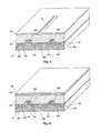
- the first intermediate semiconductor device structure 10includes a semiconductor substrate 11 having desired features, such as transistors 12 a , 12 b , source and drain regions 14 a - 14 d , isolation regions 15 a - 15 c , or other electrical features or components, already formed thereon.
- semiconductor substratesignifies any construction including semiconductive material, including, but not limited to, bulk semiconductive material, such as a semiconductive wafer, either alone or in assemblies including other materials, and semiconductive material layers, either alone or in assemblies including other materials.
- FIG. 1provides a greatly simplified illustration of a typical first intermediate semiconductor device structure 10 . It is well known in the art that an intermediate semiconductor device structure may further include other features necessary for the proper function of the completed semiconductor device, and, as will be easily appreciated from the description provided herein, application of the first embodiment of the method of the present invention is not limited to the simplified schematic representations provided in the accompanying figures.
- an etch stop layer 16is formed over the first intermediate semiconductor device structure 10 .
- the etch stop layer 16may include any suitable material, such as silicon dioxide (SiO 2 ), silicon oxynitride (Si x O y N 2 ), tetraethylorthosilicate (TEOS), or silicon nitride (Si 3 N 4 ).
- the etch stop layer 16may be formed by any well-known means, such as a chemical vapor deposition (CVD) process.
- the etch stop layer 16includes a layer of Si x O y N 2 deposited by a plasma-enhanced CVD process.
- the etch stop layer 16protects the various features included on the semiconductor substrate 11 , such as the transistors 12 a , 12 b , from degradation or damage during subsequent etch steps used to define desired local interconnects. Moreover, the etch stop layer 16 may additionally serve as a barrier layer, substantially preventing diffusion of contaminants from overlying material layers into the semiconductor substrate 11 or any features included on the semiconductor substrate 11 .
- the passivation layer 18may be composed of known silica materials, such as SiO 2 , borophosphosilicate glass (BPSG), phosphosilicate glass (PSG), borosilicate glass (BSG), or doped or undoped oxide materials.
- BPSGis the presently preferred passivation material, and where BPSG is used, the passivation layer 18 may be formed by depositing a layer of BPSG and utilizing known reflow or polishing techniques to achieve a passivation layer 18 having a desired thickness and planarity.
- the ILD 20may include any suitable dielectric material, such as SiO 2 , Si x O y N 2 , or, preferably, Si 3 N 4 . Again, the ILD material may be formed by any known process, such as known CVD processes.
- a first resist 22is formed over the ILD 20 .
- Any desirable resist materialmay be used to form the first resist 22 , and, as can also be appreciated from drawing FIG. 4 , the first resist 22 is exposed and developed according to well-known processes to define a pattern corresponding in size, shape, and location to a desired first local interconnect.
- the ILD 20is etched to define a trench 24 into the ILD 20 .
- The,trench 24will enclose and define the first local interconnect. Though any suitable etch process may be used, a dry plasma etch process is preferred. Because it is difficult to precisely control the depth of the ILD 20 etch, it is likely that the trench 24 will extend at least slightly into the passivation layer 18 , as is shown in drawing FIG. 5 .
- the first resist 22is stripped using means known in the art.
- the trench 24is then filled with a desired conductive material.
- a layer of conductive material 26such as tungsten, is formed over the trench 24 and the remaining portions of the ILD 20 by known means, such as a sputter deposition or CVD process.
- the layer of conductive material 26is then polished as known in the art, such as by a chemical mechanical planarization (CMP) process, to achieve a first local interconnect 28 , which extends through the ILD 20 but is substantially coplanar with the top surface 30 of the ILD 20 (shown in drawing FIG. 7 ).
- CMPchemical mechanical planarization
- the trench 24 defining the first local interconnect 28may be filled by first depositing a barrier layer 32 over the trench 24 and remaining portion of the ILD 20 .
- the barrier layer 32may include a first conductive material, such as titanium, tungsten, tantalum, titanium nitride, tungsten nitride, or tantalum nitride, and the barrier layer is formed by well-known means in the art. As can be seen in drawing FIG. 8 , the barrier layer 32 partially fills the trench 24 .
- a second conductive layer 34is formed over the barrier layer 32 .
- the second conductive layer 34may include any suitable material, such as tungsten, and can also be formed using well-known techniques.
- the barrier layer 32 and the second conductive layer 34are then polished by suitable means, such as a known CMP process, to again achieve a first local interconnect 28 , which extends through the ILD 20 but is substantially coplanar with the top surface 30 of the ILD 20 (shown in drawing FIG. 9 ).
- the first local interconnect 28can be sized, shaped, and positioned as desired.
- the local interconnectis sized, shaped, and positioned such that, after formation of the final stacked local interconnect structure (shown in drawing FIG. 13 and drawing FIG. 15 ), the first local interconnect 28 enables the electrical connection of a first group of interconnected electrical features (e.g., transistors 12 a and 12 b ) to one or more additional groups of interconnected electrical features (not illustrated).
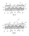
- a second resist 40is formed over the semiconductor substrate 11 , as can be seen in drawing FIG. 10 .
- any desirable resist materialmay be used to form the second resist 40 .
- the second resist 40is exposed and developed according to well-known processes to define the desired shape and location of the second and third local interconnects, which will complete the stacked local interconnect structure.
- the ILD 20 and passivation layer 18are etched to define openings 42 a , 42 b using a self-aligned contact (SAC) etch, which is selective to the material(s) used in first local interconnect 28 and etch stop layer 16 (FIG. 11 ).
- SACself-aligned contact
- the openings 42 a , 42 b formed by the SAC etchextend down through the passivation layer 18 and expose each of the electrical features, such as transistors 12 a , 12 b , which are to be electrically connected.
- the SAC etchis selective to the material used to form the first local interconnect 28 , the portion 44 of the passivation layer 18 underlying the first local interconnect 28 remains intact, providing proper isolation for each of the electrical features to be interconnected, such as transistors 12 a and 12 b , and protecting any intervening, unrelated electrical features that may be included underneath the first local interconnect 28 .
- the second resist 40is stripped using means known in the art.
- portions of the etch stop layer 16 overlying the electrical features to be interconnectedare selectively removed by a known etch process.
- the etch processis preferably a selective plasma dry etch process, such as a “punch etch” process. Illustrated in drawing FIG. 12 is an intermediate semiconductor device structure 10 after portions 46 a , 46 b of the etch stop layer 16 have been removed by a desirable etch process.
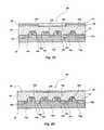
- a layer of conductive material 48is formed over openings 42 a , 42 b , the first local interconnect 28 , and the remaining portions of the ILD 20 (shown in drawing FIG. 12 ).
- the layer of conductive material 48fills openings 42 a and 42 b and may include any suitable conductive material, such as tungsten, the presently preferred material.
- the layer of conductive material 48may be formed using a known deposition process. As can be appreciated by reference to drawing FIG.
- the layer of conductive material 48is then polished as known in the art, such as by a chemical mechanical polishing (CMP) process, to achieve second and third local interconnects 50 , 51 , which extend through the ILD 20 and passivation layer 18 , are in electrical contact with the electronic features, such as transistors 12 a and 12 b , to be interconnected, are in electrical contact with the first local interconnect 28 , and are substantially coplanar with the top surface 30 of the ILD 20 (shown in drawing FIG. 13 ).
- CMPchemical mechanical polishing
- the second and third local interconnects 50 , 51may also be formed by first depositing a barrier layer 52 comprised of any suitable material, such as those materials already described in regard to first local interconnect 28 .
- the barrier layer 52partially fills openings 42 a and 42 b .
- a second conductive layer 54is formed over the semiconductor substrate 11 .
- the second conductive layer 54which can be formed using well-known techniques, completely fills openings 42 a and 42 b and may include any suitable material, such as tungsten.
- the barrier layer 52 and the second conductive layer 54are then polished by suitable means, such as a known CMP process, to achieve second and third local interconnects 50 , 51 , which extend through the ILD 20 and passivation layer 18 , are in electrical contact with the electrical features, such as transistors 12 a and 12 b to be interconnected, are in electrical contact with the first local interconnect 28 , and are substantially coplanar with the top surface 30 of the ILD 20 (shown in drawing FIG. 15 ).
- the first embodiment of the method of the present inventionprovides a stacked local interconnect structure formed of a first local interconnect 28 , a second local interconnect 50 , and a third local interconnect 51 , which enables the interconnection of two or more isolated groups of interconnected electrical features included in the same level of a multilevel IC device.
- a first group of electrical features, transistors 12 a and 12 bis electrically connected by second local interconnect 50
- a second set of electrical features(not illustrated) is electrically connected by third local interconnect 51
- the first and second groups of electrical featuresare electrically connected by first local interconnect 28 .
- the stacked local interconnects formed by the first embodiment of the present inventiondo not include multilevel metallization structures that would otherwise extend into and complicate higher levels included in a multilevel semiconductor device.
- the fabrication of the stacked local interconnectsis accomplished without contact plugs and the disadvantages that accompany the use of contact plugs, such as the need for enlarged contact pads and extra masking and etching steps. Therefore, the first embodiment of the present invention provides a method for forming stacked local interconnects that facilitate the electrical connection of isolated groups of interconnected electrical features, but the first embodiment of the method of the present invention also substantially reduces or eliminates the disadvantages associated with known multilevel interconnect structures.
- the first embodiment of the method of the present inventionhas been described herein with reference to a stacked local interconnect structure including a first local interconnect electrically connecting second and third local interconnects, the first embodiment may be used to form any desired stacked local interconnect structure.
- the first embodiment of the present inventionmay be used to form a first local interconnect electrically connecting three or more groups of electrically connected semiconductor device features.
- the first embodiment of the method of the present inventionmay be used to electrically connect a first group of electrically connected features to one or more individual electrical features.
- the first embodiment of the method of the present inventionis extremely flexible and provides a means by which a group of interconnected electrical features may be electrically connected to any desired number of isolated interconnected electrical features or individual electrical features without the need for multilevel interconnect semiconductor device structures.
- a second embodiment of the method of the present inventionis similar to the first embodiment, except that it may be used to electrically connect individual isolated electronic features.
- the first step in the second embodimentis providing an intermediate semiconductor device structure 59 (shown in drawing FIG. 16 ) including a semiconductor substrate 61 having desired electrical features, such as transistors 12 a - 12 d , source and drain regions 14 a - 14 g , or any other desired electrical features formed thereon.
- the intermediate semiconductor device structure 59 providedmay further include any other features, such as field oxide or isolation regions 15 a - 15 d , that may be necessary for the proper function of a completed IC device.
- FIG. 16like FIG. 1 , provides a greatly simplified illustration of a typical intermediate semiconductor device structure 59 .
- application of the second embodiment of the method of the present inventionis not limited to the simplified schematic representations provided in the accompanying figures.
- an etch stop layer 16is formed over the first intermediate semiconductor device structure 59 .
- the etch stop layer 16may include any suitable material, such as silicon dioxide (SiO 2 ), silicon oxynitride (Si x O y N 2 ), tetraethylorthosilicate (TEOS), or silicon nitride (Si 3 N 4 ).
- the etch stop layer 16may be formed by any well-known means, such as a chemical vapor deposition (CVD) process.
- the etch stop layer 16includes a layer of Si x O y N 2 deposited by a plasma-enhanced CVD process.
- the etch stop layer 16protects the various features included on the semiconductor substrate 61 , such as the transistors 12 a - 12 d , from degradation or damage during subsequent etch steps used to define desired local interconnects. Moreover, the etch stop layer 16 may additionally serve as a barrier layer, substantially preventing diffusion of contaminants from overlying material layers into the semiconductor substrate 61 or any features included on the semiconductor substrate 61 .
- the passivation layer 18may be composed of known silica materials, such as SiO 2 , borophosphosilicate glass (BPSG), phosphosilicate glass (PSG), borosilicate glass (BSG), or doped or undoped oxide materials.
- BPSGis the presently preferred passivation material, and where BPSG is used, the passivation layer 18 may be formed by depositing a layer of BPSG and polishing the BPSG layer, using known polishing techniques, to achieve a passivation layer 18 having a desired thickness and planarity.
- the ILD 20may include any suitable dielectric material, such as SiO 2 , Si x O y N 2 , or, preferably, Si 3 N 4 , and, again, the ILD material may be formed by any known process, such as known CVD processes.
- a first resist 60is formed over the ILD 20 .
- Any desirable resist materialmay be used to form the first resist 60 , and, as can also be appreciated from drawing FIG. 19 , the first resist 60 is exposed and developed according to well-known processes to define a pattern corresponding in size, shape, and location to a first portion of the desired stacked local interconnect.
- the ILD 20is etched to define a trench 62 into the ILD 20 , which will enclose and define the first portion of the stacked local interconnect.
- any suitable etch processmay be used, a dry plasma etch is preferred. Because it is difficult to precisely control the depth of the ILD 20 etch, it is likely that the trench 62 will extend at least slightly into the passivation layer 18 , as is shown in drawing FIG. 20 .
- the trench 62is then filled with a desired conductive material.
- a layer of conductive material 26such as tungsten, is formed over the trench 62 and the remaining portions of the ILD 20 by known means, such as a sputter deposition or CVD process.
- the deposited layer of conductive material layer 26is then polished as known in the art, such as by a chemical mechanical polishing (CMP) process, to achieve a first portion 64 of the stacked local interconnect, which extends through the ILD 20 , but is substantially coplanar with the top surface 30 of the ILD 20 (shown in drawing FIG. 22 ).
- CMPchemical mechanical polishing
- the trench 62 defining the first interconnectmay be filled by first depositing a barrier layer 32 over the trench 62 and the remaining portions of the ILD 20 .
- the barrier layer 32may include a first conductive material, such as titanium, tungsten, tantalum, titanium nitride, tungsten nitride, or tantalum nitride, and the barrier layer is formed by well-known means in the art. As can be seen in drawing FIG. 23 , the barrier layer 32 partially fills the trench 62 . After formation of the barrier layer 32 , a second conductive layer 34 , which completely fills the trench 62 , is formed over the barrier layer 32 .
- the second conductive layer 34may include any suitable material, such as tungsten, and can also be formed using well-known techniques.
- the barrier layer 32 and the second conductive layer 34are then polished by suitable means, such as a known CMP process, to again achieve a first portion 64 of a stacked local interconnect, which extends through the ILD 20 , but is substantially coplanar with the top surface 30 of the ILD 20 (shown in drawing FIG. 24 ).
- the first portion 64 of the stacked local interconnectcan be sized, shaped, and positioned as desired.
- the local interconnectis sized, shaped, and positioned such that, after formation of the final stacked local interconnect structure (shown in drawing FIG. 30 ), the first portion 64 of the stacked local interconnect enables the electrical interconnection of two or more isolated electrical features, such as transistors 12 a and 12 d.
- a second resist 66is formed over the semiconductor substrate 61 , as can be seen in drawing FIG. 25 .
- any desirable resist materialmay be used to form the second resist 66 .
- the second resist 66is exposed and developed according to well-known processes to define the desired shape and location of the second and third portions of the stacked local interconnect.
- the ILD 20 and passivation layer 18are etched to define openings 68 a , 68 b using a self-aligned contact (SAC) etch, which is selective to the material(s) used in first portion 64 of the stacked local interconnect.
- SACself-aligned contact
- the openings 68 a , 68 b formed by the SAC etchextend down through the passivation layer 18 and expose the electrical features, such as transistors 12 a and 12 d that are to be electrically connected.
- the portion 70 of the passivation layer 18 underlying the first portion 64 of the stacked local interconnectremains intact, providing proper isolation for the electrical features and protecting any intervening, unrelated electrical features, such as transistors 12 b and 12 c , that may be included underneath the first portion 64 of the stacked local interconnect.
- portions of the etch stop layer 16are first selectively removed by a known etch process.
- the etch processis preferably a selective plasma dry etch process, such as a “punch etch” process. Illustrated in drawing FIG. 27 is an intermediate semiconductor device structure 59 after portions 72 a , 72 b of the etch stop layer 16 have been removed by a desirable etch process.
- a layer of conductive material 48is formed over the openings 68 a , 68 b , the first portion 64 of the stacked local interconnect and the remaining portions of the ILD 20 (shown in drawing FIG. 27 ).
- the layer of conductive material 48may include any suitable conductive material, though tungsten is presently preferred, and the layer of conductive material 48 may be formed using known deposition processes. As can be appreciated by reference to drawing FIG.
- the deposited layer of conductive material 48is then polished as known in the art, such as by a chemical mechanical polishing (CMP) process, to achieve second and third portions 76 , 78 , which extend through the ILD 20 and passivation layer 18 , are in electrical contact with the electronic features, such as transistors 12 a and 12 d , to be interconnected, are in electrical contact with the first portion 64 of the stacked local interconnect, and are substantially coplanar with the top surface 30 of the ILD 20 .
- CMPchemical mechanical polishing
- the second and third portions 76 , 78 of the stacked local interconnectmay also be formed by first depositing a barrier layer 52 comprised of any suitable material, such as those materials already described in regard to first portion 64 of the stacked local interconnect.
- the barrier layer 52partially fills openings 68 a and 68 b .
- a second conductive layer 54is formed over the barrier layer 52 .
- the second conductive layer 54which can be formed using well-known techniques, completely fills openings 68 a and 68 b and may include any suitable material, such as tungsten.
- the barrier layer 52 and the second conductive layer 54are then polished by suitable means, such as a known CMP process, to achieve second and third portions 76 , 78 of the stacked local interconnect, which extend through the ILD 20 and passivation layer 18 , are in electrical contact with the electrical features, such as transistors 12 a and 12 d , to be interconnected, are in electrical contact with the first portion 64 of the local interconnect, and are substantially coplanar with the top surface 30 of the ILD 20 (shown in drawing FIG. 30 ).
- suitable meanssuch as a known CMP process
- FIG. 28 and drawing FIG. 30highlights the second embodiment of the method of the present invention, which provides a stacked local interconnect structure 80 formed of a first portion 64 , a second portion 76 , and a third portion 78 .
- the stacked local interconnects formed by the second embodiment of the present inventionenable the interconnection of two or more isolated electrical features included within a single level of a multilevel semiconductor device. For example, as shown in drawing FIG. 28 and drawing FIG. 30 , a first isolated transistor 12 a is electrically connected by the stacked local interconnect structure 80 to a second isolated transistor 12 d .
- the second embodiment of the method of the present inventionprovides a method for forming stacked local interconnects that facilitates the electrical connection of isolated electrical features, while substantially reducing or eliminating the disadvantages associated with known multilevel interconnect structures.
- the second embodiment of the method of the present inventionhas been described herein in relation to a stacked local interconnect structure including three portions electrically connecting two isolated electrical features, the second embodiment of the method of the present invention is extremely flexible and may be used to electrically connect any desired number of isolated electrical features.
- Both the first and the second embodiments of the method of the present inventionaccomplish the interconnection of isolated electrical features without disturbing any unrelated, intervening semiconductor device features.
- the first interconnect formed in the first embodiment and the first portion of the stacked local interconnect formed in the second embodimentprotect underlying semiconductor device features from possible damage due to loss of selectivity during subsequent etch steps or due to misalignment of masks used to create the openings used for the second and third interconnects in the first embodiment as well as the second and third portions of the stacked local interconnect of the second embodiment.
- the SAC etch employed to create such openingsis selective to the materials used to form the first local interconnect of the first embodiment or the first portion of the stacked local interconnect of the second embodiment, those features underlying the first local interconnect or first portion of the stacked local interconnect will be protected from damage during the SAC etch, even if the patterned masks used in the SAC step are misaligned or out of position. Therefore, where desired, the first local interconnect of the first embodiment of the method of the present invention or the first portion of the stacked local interconnect of the second embodiment of the method of the present invention may be shaped and positioned to specifically protect underlying semiconductor device features from subsequent fabrication steps.
- a protective overlying metallization layersuch as the first local interconnect of the first embodiment or the first portion of the stacked local interconnect of the second embodiment, may be formed over semiconductor device features to be protected by the processes taught herein.
- a protective overlying metallization layerwould be formed where there is an increased likelihood that subsequent etch steps may lose selectivity or where an error in mask formation would otherwise allow damage to underlying semiconductor device features.
Landscapes
- Engineering & Computer Science (AREA)
- Physics & Mathematics (AREA)
- Condensed Matter Physics & Semiconductors (AREA)
- General Physics & Mathematics (AREA)
- Computer Hardware Design (AREA)
- Microelectronics & Electronic Packaging (AREA)
- Power Engineering (AREA)
- Manufacturing & Machinery (AREA)
- Internal Circuitry In Semiconductor Integrated Circuit Devices (AREA)
Abstract
Description
Claims (15)
Priority Applications (2)
| Application Number | Priority Date | Filing Date | Title |
|---|---|---|---|
| US10/407,957US6858525B2 (en) | 2000-11-09 | 2003-04-04 | Stacked local interconnect structure and method of fabricating same |
| US11/050,057US7314822B2 (en) | 2000-11-09 | 2005-02-03 | Method of fabricating stacked local interconnect structure |
Applications Claiming Priority (3)
| Application Number | Priority Date | Filing Date | Title |
|---|---|---|---|
| US09/710,399US6498088B1 (en) | 2000-11-09 | 2000-11-09 | Stacked local interconnect structure and method of fabricating same |
| US10/076,792US6544881B2 (en) | 2000-11-09 | 2002-02-14 | Stacked local interconnect structure and method of fabricating same |
| US10/407,957US6858525B2 (en) | 2000-11-09 | 2003-04-04 | Stacked local interconnect structure and method of fabricating same |
Related Parent Applications (1)
| Application Number | Title | Priority Date | Filing Date |
|---|---|---|---|
| US10/076,792ContinuationUS6544881B2 (en) | 2000-11-09 | 2002-02-14 | Stacked local interconnect structure and method of fabricating same |
Related Child Applications (1)
| Application Number | Title | Priority Date | Filing Date |
|---|---|---|---|
| US11/050,057ContinuationUS7314822B2 (en) | 2000-11-09 | 2005-02-03 | Method of fabricating stacked local interconnect structure |
Publications (2)
| Publication Number | Publication Date |
|---|---|
| US20030211676A1 US20030211676A1 (en) | 2003-11-13 |
| US6858525B2true US6858525B2 (en) | 2005-02-22 |
Family
ID=24853873
Family Applications (8)
| Application Number | Title | Priority Date | Filing Date |
|---|---|---|---|
| US09/710,399Expired - LifetimeUS6498088B1 (en) | 2000-11-09 | 2000-11-09 | Stacked local interconnect structure and method of fabricating same |
| US09/892,956Expired - LifetimeUS6482689B2 (en) | 2000-11-09 | 2001-06-27 | Stacked local interconnect structure and method of fabricating same |
| US10/050,630Expired - Fee RelatedUS6555478B2 (en) | 2000-11-09 | 2002-01-15 | Stacked local interconnect structure and method of fabricating same |
| US10/076,792Expired - LifetimeUS6544881B2 (en) | 2000-11-09 | 2002-02-14 | Stacked local interconnect structure and method of fabricating same |
| US10/407,642Expired - Fee RelatedUS6831001B2 (en) | 2000-11-09 | 2003-04-04 | Method of fabricating a stacked local interconnect structure |
| US10/407,957Expired - LifetimeUS6858525B2 (en) | 2000-11-09 | 2003-04-04 | Stacked local interconnect structure and method of fabricating same |
| US11/011,525AbandonedUS20050095848A1 (en) | 2000-11-09 | 2004-12-14 | Method of fabricating a stacked local interconnect structure |
| US11/050,057Expired - LifetimeUS7314822B2 (en) | 2000-11-09 | 2005-02-03 | Method of fabricating stacked local interconnect structure |
Family Applications Before (5)
| Application Number | Title | Priority Date | Filing Date |
|---|---|---|---|
| US09/710,399Expired - LifetimeUS6498088B1 (en) | 2000-11-09 | 2000-11-09 | Stacked local interconnect structure and method of fabricating same |
| US09/892,956Expired - LifetimeUS6482689B2 (en) | 2000-11-09 | 2001-06-27 | Stacked local interconnect structure and method of fabricating same |
| US10/050,630Expired - Fee RelatedUS6555478B2 (en) | 2000-11-09 | 2002-01-15 | Stacked local interconnect structure and method of fabricating same |
| US10/076,792Expired - LifetimeUS6544881B2 (en) | 2000-11-09 | 2002-02-14 | Stacked local interconnect structure and method of fabricating same |
| US10/407,642Expired - Fee RelatedUS6831001B2 (en) | 2000-11-09 | 2003-04-04 | Method of fabricating a stacked local interconnect structure |
Family Applications After (2)
| Application Number | Title | Priority Date | Filing Date |
|---|---|---|---|
| US11/011,525AbandonedUS20050095848A1 (en) | 2000-11-09 | 2004-12-14 | Method of fabricating a stacked local interconnect structure |
| US11/050,057Expired - LifetimeUS7314822B2 (en) | 2000-11-09 | 2005-02-03 | Method of fabricating stacked local interconnect structure |
Country Status (1)
| Country | Link |
|---|---|
| US (8) | US6498088B1 (en) |
Families Citing this family (15)
| Publication number | Priority date | Publication date | Assignee | Title |
|---|---|---|---|---|
| US6498088B1 (en)* | 2000-11-09 | 2002-12-24 | Micron Technology, Inc. | Stacked local interconnect structure and method of fabricating same |
| KR100421048B1 (en)* | 2001-09-07 | 2004-03-04 | 삼성전자주식회사 | Semiconductor device having local interconnection layer & fabricating method thereof |
| US7081398B2 (en) | 2001-10-12 | 2006-07-25 | Micron Technology, Inc. | Methods of forming a conductive line |
| US7179691B1 (en)* | 2002-07-29 | 2007-02-20 | Taiwan Semiconductor Manufacturing Co., Ltd. | Method for four direction low capacitance ESD protection |
| US6974770B2 (en)* | 2003-06-20 | 2005-12-13 | Infineon Technologies Ag | Self-aligned mask to reduce cell layout area |
| US7118966B2 (en)* | 2004-08-23 | 2006-10-10 | Micron Technology, Inc. | Methods of forming conductive lines |
| US7037774B1 (en) | 2004-10-21 | 2006-05-02 | Integrated Device Technology, Inc. | Self-aligned contact structure and process for forming self-aligned contact structure |
| US7956421B2 (en) | 2008-03-13 | 2011-06-07 | Tela Innovations, Inc. | Cross-coupled transistor layouts in restricted gate level layout architecture |
| US7446352B2 (en) | 2006-03-09 | 2008-11-04 | Tela Innovations, Inc. | Dynamic array architecture |
| US8541879B2 (en) | 2007-12-13 | 2013-09-24 | Tela Innovations, Inc. | Super-self-aligned contacts and method for making the same |
| US7763534B2 (en)* | 2007-10-26 | 2010-07-27 | Tela Innovations, Inc. | Methods, structures and designs for self-aligning local interconnects used in integrated circuits |
| US9563733B2 (en) | 2009-05-06 | 2017-02-07 | Tela Innovations, Inc. | Cell circuit and layout with linear finfet structures |
| TWI388015B (en)* | 2009-10-08 | 2013-03-01 | Chunghwa Picture Tubes Ltd | Thin film transistor and method of manufacturing same |
| CN103578919A (en)* | 2012-07-26 | 2014-02-12 | 无锡华润上华科技有限公司 | Method for forming passivation layer of MOS device and MOS device |
| US10910216B2 (en) | 2017-11-28 | 2021-02-02 | Taiwan Semiconductor Manufacturing Co., Ltd. | Low-k dielectric and processes for forming same |
Citations (79)
| Publication number | Priority date | Publication date | Assignee | Title |
|---|---|---|---|---|
| US3904454A (en) | 1973-12-26 | 1975-09-09 | Ibm | Method for fabricating minute openings in insulating layers during the formation of integrated circuits |
| US4543707A (en)* | 1983-06-30 | 1985-10-01 | Kabushiki Kaisha | Method of forming through holes by differential etching of stacked silicon oxynitride layers |
| JPS63253661A (en) | 1987-04-10 | 1988-10-20 | Oki Electric Ind Co Ltd | Manufacture of semiconductor memory device |
| US4789648A (en)* | 1985-10-28 | 1988-12-06 | International Business Machines Corporation | Method for producing coplanar multi-level metal/insulator films on a substrate and for forming patterned conductive lines simultaneously with stud vias |
| US4808552A (en) | 1985-09-11 | 1989-02-28 | Texas Instruments Incorporated | Process for making vertically-oriented interconnections for VLSI devices |
| JPH02275665A (en) | 1988-12-08 | 1990-11-09 | Mitsubishi Electric Corp | Semiconductor storage device and its manufacturing method |
| US5013680A (en) | 1990-07-18 | 1991-05-07 | Micron Technology, Inc. | Process for fabricating a DRAM array having feature widths that transcend the resolution limit of available photolithography |
| US5030585A (en) | 1990-03-22 | 1991-07-09 | Micron Technology, Inc. | Split-polysilicon CMOS DRAM process incorporating selective self-aligned silicidation of conductive regions and nitride blanket protection of N-channel regions during P-channel gate spacer formation |
| US5049517A (en)* | 1990-11-07 | 1991-09-17 | Micron Technology, Inc. | Method for formation of a stacked capacitor |
| US5061650A (en) | 1991-01-17 | 1991-10-29 | Micron Technology, Inc. | Method for formation of a stacked capacitor |
| US5061651A (en) | 1987-12-11 | 1991-10-29 | Oki Electric Industry Co., Ltd. | Method of making dram cell with stacked capacitor |
| US5068199A (en) | 1991-05-06 | 1991-11-26 | Micron Technology, Inc. | Method for anodizing a polysilicon layer lower capacitor plate of a DRAM to increase capacitance |
| US5077238A (en) | 1988-05-18 | 1991-12-31 | Mitsubishi Denki Kabushiki Kaisha | Method of manufacturing a semiconductor device with a planar interlayer insulating film |
| US5082797A (en) | 1991-01-22 | 1992-01-21 | Micron Technology, Inc. | Method of making stacked textured container capacitor |
| US5091339A (en) | 1990-07-23 | 1992-02-25 | Microelectronics And Computer Technology Corporation | Trenching techniques for forming vias and channels in multilayer electrical interconnects |
| JPH0469964A (en) | 1990-07-10 | 1992-03-05 | Fujitsu Ltd | Manufacturing method of semiconductor device |
| US5110752A (en) | 1991-07-10 | 1992-05-05 | Industrial Technology Research Institute | Roughened polysilicon surface capacitor electrode plate for high denity dram |
| US5134085A (en) | 1991-11-21 | 1992-07-28 | Micron Technology, Inc. | Reduced-mask, split-polysilicon CMOS process, incorporating stacked-capacitor cells, for fabricating multi-megabit dynamic random access memories |
| US5135881A (en) | 1990-09-27 | 1992-08-04 | Nec Corporation | Method of making random access memory device having memory cells each implemented by a stacked storage capacitor and a transfer transistor with lightly-doped drain structure |
| US5138411A (en) | 1991-05-06 | 1992-08-11 | Micron Technology, Inc. | Anodized polysilicon layer lower capacitor plate of a dram to increase capacitance |
| US5150276A (en) | 1992-01-24 | 1992-09-22 | Micron Technology, Inc. | Method of fabricating a vertical parallel cell capacitor having a storage node capacitor plate comprising a center fin effecting electrical communication between itself and parallel annular rings |
| US5162248A (en) | 1992-03-13 | 1992-11-10 | Micron Technology, Inc. | Optimized container stacked capacitor DRAM cell utilizing sacrificial oxide deposition and chemical mechanical polishing |
| US5164337A (en) | 1989-11-01 | 1992-11-17 | Matsushita Electric Industrial Co., Ltd. | Method of fabricating a semiconductor device having a capacitor in a stacked memory cell |
| US5168073A (en) | 1991-10-31 | 1992-12-01 | Micron Technology, Inc. | Method for fabricating storage node capacitor having tungsten and etched tin storage node capacitor plate |
| US5170233A (en) | 1991-03-19 | 1992-12-08 | Micron Technology, Inc. | Method for increasing capacitive surface area of a conductive material in semiconductor processing and stacked memory cell capacitor |
| US5185282A (en) | 1989-11-23 | 1993-02-09 | Electronics And Telecommunications Research Institute | Method of manufacturing DRAM cell having a cup shaped polysilicon storage electrode |
| US5206787A (en) | 1991-04-01 | 1993-04-27 | Fujitsu Limited | Capacitor and method of fabricating same |
| JPH05129548A (en) | 1991-11-01 | 1993-05-25 | Hitachi Ltd | Semiconductor device and manufacturing method thereof |
| US5227651A (en) | 1991-03-23 | 1993-07-13 | Samsung Electronics, Co., Ltd. | Semiconductor device having a capacitor with an electrode grown through pinholes |
| US5229314A (en) | 1990-05-01 | 1993-07-20 | Mitsubishi Denki Kabushiki Kaisha | Method of manufacturing field effect transistor having a multilayer interconnection layer therein with tapered sidewall insulation |
| US5238862A (en) | 1992-03-18 | 1993-08-24 | Micron Technology, Inc. | Method of forming a stacked capacitor with striated electrode |
| US5240871A (en) | 1991-09-06 | 1993-08-31 | Micron Technology, Inc. | Corrugated storage contact capacitor and method for forming a corrugated storage contact capacitor |
| EP0557590A1 (en) | 1992-02-28 | 1993-09-01 | Samsung Electronics Co. Ltd. | Method for manufacturing a capacitor of a semiconductor device |
| US5244837A (en) | 1993-03-19 | 1993-09-14 | Micron Semiconductor, Inc. | Semiconductor electrical interconnection methods |
| JPH05315586A (en) | 1992-05-11 | 1993-11-26 | Mitsubishi Electric Corp | Manufacture of charge-transfer device |
| US5270241A (en) | 1992-03-13 | 1993-12-14 | Micron Technology, Inc. | Optimized container stacked capacitor DRAM cell utilizing sacrificial oxide deposition and chemical mechanical polishing |
| US5292677A (en) | 1992-09-18 | 1994-03-08 | Micron Technology, Inc. | Reduced mask CMOS process for fabricating stacked capacitor multi-megabit dynamic random access memories utilizing single etch stop layer for contacts |
| US5338700A (en) | 1993-04-14 | 1994-08-16 | Micron Semiconductor, Inc. | Method of forming a bit line over capacitor array of memory cells |
| US5340765A (en) | 1993-08-13 | 1994-08-23 | Micron Semiconductor, Inc. | Method for forming enhanced capacitance stacked capacitor structures using hemi-spherical grain polysilicon |
| US5340763A (en) | 1993-02-12 | 1994-08-23 | Micron Semiconductor, Inc. | Multi-pin stacked capacitor utilizing micro villus patterning in a container cell and method to fabricate same |
| US5354711A (en) | 1990-06-26 | 1994-10-11 | Commissariat A L'energie Atomique | Process for etching and depositing integrated circuit interconnections and contacts |
| US5354705A (en) | 1993-09-15 | 1994-10-11 | Micron Semiconductor, Inc. | Technique to fabricate a container structure with rough inner and outer surfaces |
| US5362666A (en) | 1992-09-18 | 1994-11-08 | Micron Technology, Inc. | Method of producing a self-aligned contact penetrating cell plate |
| US5436183A (en) | 1990-04-17 | 1995-07-25 | National Semiconductor Corporation | Electrostatic discharge protection transistor element fabrication process |
| US5447878A (en) | 1992-09-19 | 1995-09-05 | Samsung Electronics Co., Ltd. | Method for manufacturing a semiconductor memory device having a capacitor with increased effective area |
| US5457063A (en) | 1993-04-20 | 1995-10-10 | Hyundai Electronics Industries Co., Ltd. | Method for fabricating a capacitor for a dynamic random access memory cell |
| US5459094A (en) | 1994-01-12 | 1995-10-17 | Goldstar Electron Co., Ltd. | Method for fabricating a capacitor cell in the semiconductor memory device having a step portion |
| US5478772A (en) | 1993-04-02 | 1995-12-26 | Micron Technology, Inc. | Method for forming a storage cell capacitor compatible with high dielectric constant materials |
| US5491356A (en) | 1990-11-19 | 1996-02-13 | Micron Technology, Inc. | Capacitor structures for dynamic random access memory cells |
| US5494841A (en) | 1993-10-15 | 1996-02-27 | Micron Semiconductor, Inc. | Split-polysilicon CMOS process for multi-megabit dynamic memories incorporating stacked container capacitor cells |
| US5508223A (en) | 1995-05-05 | 1996-04-16 | Vanguard International Semiconductor Corporation | Method for manufacturing DRAM cell with fork-shaped capacitor |
| US5519238A (en) | 1991-10-02 | 1996-05-21 | Industrial Technology Research Institute | Rippled polysilicon surface capacitor electrode plate for high density dram |
| US5518948A (en) | 1995-09-27 | 1996-05-21 | Micron Technology, Inc. | Method of making cup-shaped DRAM capacitor having an inwardly overhanging lip |
| US5563762A (en) | 1994-11-28 | 1996-10-08 | Northern Telecom Limited | Capacitor for an integrated circuit and method of formation thereof, and a method of adding on-chip capacitors to an integrated circuit |
| US5597756A (en) | 1995-06-21 | 1997-01-28 | Micron Technology, Inc. | Process for fabricating a cup-shaped DRAM capacitor using a multi-layer partly-sacrificial stack |
| US5612254A (en)* | 1992-06-29 | 1997-03-18 | Intel Corporation | Methods of forming an interconnect on a semiconductor substrate |
| US5623243A (en) | 1990-03-20 | 1997-04-22 | Nec Corporation | Semiconductor device having polycrystalline silicon layer with uneven surface defined by hemispherical or mushroom like shape silicon grain |
| US5652165A (en) | 1996-06-10 | 1997-07-29 | Vanguard International Semiconductor Corporation | Method of forming a stacked capacitor with a double wall crown shape |
| US5654589A (en) | 1995-06-06 | 1997-08-05 | Advanced Micro Devices, Incorporated | Landing pad technology doubled up as local interconnect and borderless contact for deep sub-half micrometer IC application |
| US5654238A (en) | 1995-08-03 | 1997-08-05 | International Business Machines Corporation | Method for etching vertical contact holes without substrate damage caused by directional etching |
| US5674756A (en) | 1994-07-29 | 1997-10-07 | Mitsubishi Materialc Corporation | Method for intrinsic-gettering silicon wafer |
| US5702968A (en) | 1996-01-11 | 1997-12-30 | Vanguard International Semiconductor Corporation | Method for fabricating a honeycomb shaped capacitor |
| US5798568A (en) | 1996-08-26 | 1998-08-25 | Motorola, Inc. | Semiconductor component with multi-level interconnect system and method of manufacture |
| US5847463A (en) | 1997-08-22 | 1998-12-08 | Micron Technology, Inc. | Local interconnect comprising titanium nitride barrier layer |
| US5886411A (en) | 1996-07-12 | 1999-03-23 | Kabushiki Kaisha Toshiba | Semiconductor device using dual damascene technology and method for manufacturing the same |
| US5907781A (en) | 1998-03-27 | 1999-05-25 | Advanced Micro Devices, Inc. | Process for fabricating an integrated circuit with a self-aligned contact |
| US5926709A (en) | 1995-03-30 | 1999-07-20 | Nec Corporation | Process of fabricating miniature memory cell having storage capacitor with wide surface area |
| US5933364A (en) | 1998-03-23 | 1999-08-03 | Matsushita Electric Industrial Co., Ltd. | Semiconductor device with a metal layer for supplying a predetermined potential to a memory cell section |
| US5932491A (en) | 1997-02-06 | 1999-08-03 | Micron Technology, Inc. | Reduction of contact size utilizing formation of spacer material over resist pattern |
| US5946571A (en) | 1997-08-29 | 1999-08-31 | United Microelectronics Corp. | Method of forming a capacitor |
| US5946566A (en) | 1996-03-01 | 1999-08-31 | Ace Memory, Inc. | Method of making a smaller geometry high capacity stacked DRAM device |
| US5945707A (en) | 1998-04-07 | 1999-08-31 | International Business Machines Corporation | DRAM cell with grooved transfer device |
| US5970375A (en) | 1997-05-03 | 1999-10-19 | Advanced Micro Devices, Inc. | Semiconductor fabrication employing a local interconnect |
| US6063656A (en) | 1997-04-18 | 2000-05-16 | Micron Technology, Inc. | Cell capacitors, memory cells, memory arrays, and method of fabrication |
| US6187615B1 (en) | 1998-08-28 | 2001-02-13 | Samsung Electronics Co., Ltd. | Chip scale packages and methods for manufacturing the chip scale packages at wafer level |
| US6207546B1 (en) | 1998-08-28 | 2001-03-27 | Taiwan Semiconductor Manufacturing Company | Prevent passivation from keyhole damage and resist extrusion by a crosslinking mechanism |
| US6291281B1 (en) | 1999-09-28 | 2001-09-18 | United Microelectronics Corp. | Method of fabricating protection structure |
| US6303999B1 (en) | 1997-12-12 | 2001-10-16 | Samsung Electronics Co., Ltd. | Interconnect structure with a passivation layer and chip pad |
| US6482689B2 (en) | 2000-11-09 | 2002-11-19 | Micron Technology, Inc. | Stacked local interconnect structure and method of fabricating same |
Family Cites Families (15)
| Publication number | Priority date | Publication date | Assignee | Title |
|---|---|---|---|---|
| US3604454A (en)* | 1969-10-27 | 1971-09-14 | Meyer Products Inc | Hydraulic and electric control device |
| US5206757A (en)* | 1992-02-13 | 1993-04-27 | Billy Cheng | Collapsible field glasses |
| JP3034377B2 (en) | 1992-05-12 | 2000-04-17 | 宮崎沖電気株式会社 | Method for manufacturing capacitor electrode in semiconductor device |
| US5451543A (en)* | 1994-04-25 | 1995-09-19 | Motorola, Inc. | Straight sidewall profile contact opening to underlying interconnect and method for making the same |
| JP3623834B2 (en) | 1995-01-31 | 2005-02-23 | 富士通株式会社 | Semiconductor memory device and manufacturing method thereof |
| US5756396A (en)* | 1996-05-06 | 1998-05-26 | Taiwan Semiconductor Manufacturing Company Ltd | Method of making a multi-layer wiring structure having conductive sidewall etch stoppers and a stacked plug interconnect |
| US5744865A (en)* | 1996-10-22 | 1998-04-28 | Texas Instruments Incorporated | Highly thermally conductive interconnect structure for intergrated circuits |
| US6362527B1 (en)* | 1996-11-21 | 2002-03-26 | Advanced Micro Devices, Inc. | Borderless vias on bottom metal |
| US6190966B1 (en)* | 1997-03-25 | 2001-02-20 | Vantis Corporation | Process for fabricating semiconductor memory device with high data retention including silicon nitride etch stop layer formed at high temperature with low hydrogen ion concentration |
| US5915167A (en)* | 1997-04-04 | 1999-06-22 | Elm Technology Corporation | Three dimensional structure memory |
| US6143640A (en)* | 1997-09-23 | 2000-11-07 | International Business Machines Corporation | Method of fabricating a stacked via in copper/polyimide beol |
| US6133128A (en)* | 1997-12-30 | 2000-10-17 | Intel Corporation | Method for patterning polysilicon gate layer based on a photodefinable hard mask process |
| US6174803B1 (en)* | 1998-09-16 | 2001-01-16 | Vsli Technology | Integrated circuit device interconnection techniques |
| US6417094B1 (en)* | 1998-12-31 | 2002-07-09 | Newport Fab, Llc | Dual-damascene interconnect structures and methods of fabricating same |
| US6159839A (en)* | 1999-02-11 | 2000-12-12 | Vanguard International Semiconductor Corporation | Method for fabricating borderless and self-aligned polysilicon and metal contact landing plugs for multilevel interconnections |
- 2000
- 2000-11-09USUS09/710,399patent/US6498088B1/ennot_activeExpired - Lifetime
- 2001
- 2001-06-27USUS09/892,956patent/US6482689B2/ennot_activeExpired - Lifetime
- 2002
- 2002-01-15USUS10/050,630patent/US6555478B2/ennot_activeExpired - Fee Related
- 2002-02-14USUS10/076,792patent/US6544881B2/ennot_activeExpired - Lifetime
- 2003
- 2003-04-04USUS10/407,642patent/US6831001B2/ennot_activeExpired - Fee Related
- 2003-04-04USUS10/407,957patent/US6858525B2/ennot_activeExpired - Lifetime
- 2004
- 2004-12-14USUS11/011,525patent/US20050095848A1/ennot_activeAbandoned
- 2005
- 2005-02-03USUS11/050,057patent/US7314822B2/ennot_activeExpired - Lifetime
Patent Citations (83)
| Publication number | Priority date | Publication date | Assignee | Title |
|---|---|---|---|---|
| US3904454A (en) | 1973-12-26 | 1975-09-09 | Ibm | Method for fabricating minute openings in insulating layers during the formation of integrated circuits |
| US4543707A (en)* | 1983-06-30 | 1985-10-01 | Kabushiki Kaisha | Method of forming through holes by differential etching of stacked silicon oxynitride layers |
| US4808552A (en) | 1985-09-11 | 1989-02-28 | Texas Instruments Incorporated | Process for making vertically-oriented interconnections for VLSI devices |
| US4789648A (en)* | 1985-10-28 | 1988-12-06 | International Business Machines Corporation | Method for producing coplanar multi-level metal/insulator films on a substrate and for forming patterned conductive lines simultaneously with stud vias |
| JPS63253661A (en) | 1987-04-10 | 1988-10-20 | Oki Electric Ind Co Ltd | Manufacture of semiconductor memory device |
| US5061651A (en) | 1987-12-11 | 1991-10-29 | Oki Electric Industry Co., Ltd. | Method of making dram cell with stacked capacitor |
| US5077238A (en) | 1988-05-18 | 1991-12-31 | Mitsubishi Denki Kabushiki Kaisha | Method of manufacturing a semiconductor device with a planar interlayer insulating film |
| JPH02275665A (en) | 1988-12-08 | 1990-11-09 | Mitsubishi Electric Corp | Semiconductor storage device and its manufacturing method |
| US5164337A (en) | 1989-11-01 | 1992-11-17 | Matsushita Electric Industrial Co., Ltd. | Method of fabricating a semiconductor device having a capacitor in a stacked memory cell |
| US5185282A (en) | 1989-11-23 | 1993-02-09 | Electronics And Telecommunications Research Institute | Method of manufacturing DRAM cell having a cup shaped polysilicon storage electrode |
| US5623243A (en) | 1990-03-20 | 1997-04-22 | Nec Corporation | Semiconductor device having polycrystalline silicon layer with uneven surface defined by hemispherical or mushroom like shape silicon grain |
| US5030585A (en) | 1990-03-22 | 1991-07-09 | Micron Technology, Inc. | Split-polysilicon CMOS DRAM process incorporating selective self-aligned silicidation of conductive regions and nitride blanket protection of N-channel regions during P-channel gate spacer formation |
| US5436183A (en) | 1990-04-17 | 1995-07-25 | National Semiconductor Corporation | Electrostatic discharge protection transistor element fabrication process |
| US5229314A (en) | 1990-05-01 | 1993-07-20 | Mitsubishi Denki Kabushiki Kaisha | Method of manufacturing field effect transistor having a multilayer interconnection layer therein with tapered sidewall insulation |
| US5354711A (en) | 1990-06-26 | 1994-10-11 | Commissariat A L'energie Atomique | Process for etching and depositing integrated circuit interconnections and contacts |
| JPH0469964A (en) | 1990-07-10 | 1992-03-05 | Fujitsu Ltd | Manufacturing method of semiconductor device |
| US5013680A (en) | 1990-07-18 | 1991-05-07 | Micron Technology, Inc. | Process for fabricating a DRAM array having feature widths that transcend the resolution limit of available photolithography |
| US5091339A (en) | 1990-07-23 | 1992-02-25 | Microelectronics And Computer Technology Corporation | Trenching techniques for forming vias and channels in multilayer electrical interconnects |
| US5135881A (en) | 1990-09-27 | 1992-08-04 | Nec Corporation | Method of making random access memory device having memory cells each implemented by a stacked storage capacitor and a transfer transistor with lightly-doped drain structure |
| US5049517A (en)* | 1990-11-07 | 1991-09-17 | Micron Technology, Inc. | Method for formation of a stacked capacitor |
| US5491356A (en) | 1990-11-19 | 1996-02-13 | Micron Technology, Inc. | Capacitor structures for dynamic random access memory cells |
| US5061650A (en) | 1991-01-17 | 1991-10-29 | Micron Technology, Inc. | Method for formation of a stacked capacitor |
| US5082797A (en) | 1991-01-22 | 1992-01-21 | Micron Technology, Inc. | Method of making stacked textured container capacitor |
| US5170233A (en) | 1991-03-19 | 1992-12-08 | Micron Technology, Inc. | Method for increasing capacitive surface area of a conductive material in semiconductor processing and stacked memory cell capacitor |
| US5227651A (en) | 1991-03-23 | 1993-07-13 | Samsung Electronics, Co., Ltd. | Semiconductor device having a capacitor with an electrode grown through pinholes |
| US5206787A (en) | 1991-04-01 | 1993-04-27 | Fujitsu Limited | Capacitor and method of fabricating same |
| US5068199A (en) | 1991-05-06 | 1991-11-26 | Micron Technology, Inc. | Method for anodizing a polysilicon layer lower capacitor plate of a DRAM to increase capacitance |
| US5138411A (en) | 1991-05-06 | 1992-08-11 | Micron Technology, Inc. | Anodized polysilicon layer lower capacitor plate of a dram to increase capacitance |
| US5110752A (en) | 1991-07-10 | 1992-05-05 | Industrial Technology Research Institute | Roughened polysilicon surface capacitor electrode plate for high denity dram |
| US5240871A (en) | 1991-09-06 | 1993-08-31 | Micron Technology, Inc. | Corrugated storage contact capacitor and method for forming a corrugated storage contact capacitor |
| US5519238A (en) | 1991-10-02 | 1996-05-21 | Industrial Technology Research Institute | Rippled polysilicon surface capacitor electrode plate for high density dram |
| US5168073A (en) | 1991-10-31 | 1992-12-01 | Micron Technology, Inc. | Method for fabricating storage node capacitor having tungsten and etched tin storage node capacitor plate |
| JPH05129548A (en) | 1991-11-01 | 1993-05-25 | Hitachi Ltd | Semiconductor device and manufacturing method thereof |
| US5134085A (en) | 1991-11-21 | 1992-07-28 | Micron Technology, Inc. | Reduced-mask, split-polysilicon CMOS process, incorporating stacked-capacitor cells, for fabricating multi-megabit dynamic random access memories |
| US5150276A (en) | 1992-01-24 | 1992-09-22 | Micron Technology, Inc. | Method of fabricating a vertical parallel cell capacitor having a storage node capacitor plate comprising a center fin effecting electrical communication between itself and parallel annular rings |
| EP0557590A1 (en) | 1992-02-28 | 1993-09-01 | Samsung Electronics Co. Ltd. | Method for manufacturing a capacitor of a semiconductor device |
| US5270241A (en) | 1992-03-13 | 1993-12-14 | Micron Technology, Inc. | Optimized container stacked capacitor DRAM cell utilizing sacrificial oxide deposition and chemical mechanical polishing |
| US5162248A (en) | 1992-03-13 | 1992-11-10 | Micron Technology, Inc. | Optimized container stacked capacitor DRAM cell utilizing sacrificial oxide deposition and chemical mechanical polishing |
| US5238862A (en) | 1992-03-18 | 1993-08-24 | Micron Technology, Inc. | Method of forming a stacked capacitor with striated electrode |
| JPH05315586A (en) | 1992-05-11 | 1993-11-26 | Mitsubishi Electric Corp | Manufacture of charge-transfer device |
| US5612254A (en)* | 1992-06-29 | 1997-03-18 | Intel Corporation | Methods of forming an interconnect on a semiconductor substrate |
| USRE36644E (en) | 1992-09-18 | 2000-04-04 | Micron Technology, Inc. | Tapered via, structures made therewith, and methods of producing same |
| US5362666A (en) | 1992-09-18 | 1994-11-08 | Micron Technology, Inc. | Method of producing a self-aligned contact penetrating cell plate |
| US5292677A (en) | 1992-09-18 | 1994-03-08 | Micron Technology, Inc. | Reduced mask CMOS process for fabricating stacked capacitor multi-megabit dynamic random access memories utilizing single etch stop layer for contacts |
| US5447878A (en) | 1992-09-19 | 1995-09-05 | Samsung Electronics Co., Ltd. | Method for manufacturing a semiconductor memory device having a capacitor with increased effective area |
| US5340763A (en) | 1993-02-12 | 1994-08-23 | Micron Semiconductor, Inc. | Multi-pin stacked capacitor utilizing micro villus patterning in a container cell and method to fabricate same |
| US5244837A (en) | 1993-03-19 | 1993-09-14 | Micron Semiconductor, Inc. | Semiconductor electrical interconnection methods |
| US5478772A (en) | 1993-04-02 | 1995-12-26 | Micron Technology, Inc. | Method for forming a storage cell capacitor compatible with high dielectric constant materials |
| US5338700A (en) | 1993-04-14 | 1994-08-16 | Micron Semiconductor, Inc. | Method of forming a bit line over capacitor array of memory cells |
| US5457063A (en) | 1993-04-20 | 1995-10-10 | Hyundai Electronics Industries Co., Ltd. | Method for fabricating a capacitor for a dynamic random access memory cell |
| US5340765A (en) | 1993-08-13 | 1994-08-23 | Micron Semiconductor, Inc. | Method for forming enhanced capacitance stacked capacitor structures using hemi-spherical grain polysilicon |
| US5354705A (en) | 1993-09-15 | 1994-10-11 | Micron Semiconductor, Inc. | Technique to fabricate a container structure with rough inner and outer surfaces |
| US5494841A (en) | 1993-10-15 | 1996-02-27 | Micron Semiconductor, Inc. | Split-polysilicon CMOS process for multi-megabit dynamic memories incorporating stacked container capacitor cells |
| US5459094A (en) | 1994-01-12 | 1995-10-17 | Goldstar Electron Co., Ltd. | Method for fabricating a capacitor cell in the semiconductor memory device having a step portion |
| US5674756A (en) | 1994-07-29 | 1997-10-07 | Mitsubishi Materialc Corporation | Method for intrinsic-gettering silicon wafer |
| US5563762A (en) | 1994-11-28 | 1996-10-08 | Northern Telecom Limited | Capacitor for an integrated circuit and method of formation thereof, and a method of adding on-chip capacitors to an integrated circuit |
| US5926709A (en) | 1995-03-30 | 1999-07-20 | Nec Corporation | Process of fabricating miniature memory cell having storage capacitor with wide surface area |
| US5508223A (en) | 1995-05-05 | 1996-04-16 | Vanguard International Semiconductor Corporation | Method for manufacturing DRAM cell with fork-shaped capacitor |
| US5654589A (en) | 1995-06-06 | 1997-08-05 | Advanced Micro Devices, Incorporated | Landing pad technology doubled up as local interconnect and borderless contact for deep sub-half micrometer IC application |
| US5597756A (en) | 1995-06-21 | 1997-01-28 | Micron Technology, Inc. | Process for fabricating a cup-shaped DRAM capacitor using a multi-layer partly-sacrificial stack |
| US5654238A (en) | 1995-08-03 | 1997-08-05 | International Business Machines Corporation | Method for etching vertical contact holes without substrate damage caused by directional etching |
| US5518948A (en) | 1995-09-27 | 1996-05-21 | Micron Technology, Inc. | Method of making cup-shaped DRAM capacitor having an inwardly overhanging lip |
| US5702968A (en) | 1996-01-11 | 1997-12-30 | Vanguard International Semiconductor Corporation | Method for fabricating a honeycomb shaped capacitor |
| US5946566A (en) | 1996-03-01 | 1999-08-31 | Ace Memory, Inc. | Method of making a smaller geometry high capacity stacked DRAM device |
| US5652165A (en) | 1996-06-10 | 1997-07-29 | Vanguard International Semiconductor Corporation | Method of forming a stacked capacitor with a double wall crown shape |
| US5886411A (en) | 1996-07-12 | 1999-03-23 | Kabushiki Kaisha Toshiba | Semiconductor device using dual damascene technology and method for manufacturing the same |
| US5798568A (en) | 1996-08-26 | 1998-08-25 | Motorola, Inc. | Semiconductor component with multi-level interconnect system and method of manufacture |
| US5932491A (en) | 1997-02-06 | 1999-08-03 | Micron Technology, Inc. | Reduction of contact size utilizing formation of spacer material over resist pattern |
| US6063656A (en) | 1997-04-18 | 2000-05-16 | Micron Technology, Inc. | Cell capacitors, memory cells, memory arrays, and method of fabrication |
| US5970375A (en) | 1997-05-03 | 1999-10-19 | Advanced Micro Devices, Inc. | Semiconductor fabrication employing a local interconnect |
| US5847463A (en) | 1997-08-22 | 1998-12-08 | Micron Technology, Inc. | Local interconnect comprising titanium nitride barrier layer |
| US5981380A (en) | 1997-08-22 | 1999-11-09 | Micron Technology, Inc. | Method of forming a local interconnect including selectively etched conductive layers and recess formation |
| US5946571A (en) | 1997-08-29 | 1999-08-31 | United Microelectronics Corp. | Method of forming a capacitor |
| US6303999B1 (en) | 1997-12-12 | 2001-10-16 | Samsung Electronics Co., Ltd. | Interconnect structure with a passivation layer and chip pad |
| US5933364A (en) | 1998-03-23 | 1999-08-03 | Matsushita Electric Industrial Co., Ltd. | Semiconductor device with a metal layer for supplying a predetermined potential to a memory cell section |
| US5907781A (en) | 1998-03-27 | 1999-05-25 | Advanced Micro Devices, Inc. | Process for fabricating an integrated circuit with a self-aligned contact |
| US5945707A (en) | 1998-04-07 | 1999-08-31 | International Business Machines Corporation | DRAM cell with grooved transfer device |
| US6187615B1 (en) | 1998-08-28 | 2001-02-13 | Samsung Electronics Co., Ltd. | Chip scale packages and methods for manufacturing the chip scale packages at wafer level |
| US6207546B1 (en) | 1998-08-28 | 2001-03-27 | Taiwan Semiconductor Manufacturing Company | Prevent passivation from keyhole damage and resist extrusion by a crosslinking mechanism |
| US6291281B1 (en) | 1999-09-28 | 2001-09-18 | United Microelectronics Corp. | Method of fabricating protection structure |
| US6482689B2 (en) | 2000-11-09 | 2002-11-19 | Micron Technology, Inc. | Stacked local interconnect structure and method of fabricating same |
| US6498088B1 (en)* | 2000-11-09 | 2002-12-24 | Micron Technology, Inc. | Stacked local interconnect structure and method of fabricating same |
| US6544881B2 (en)* | 2000-11-09 | 2003-04-08 | Micron Technology, Inc. | Stacked local interconnect structure and method of fabricating same |
Non-Patent Citations (9)
| Title |
|---|
| Abstract, EP000557590A1, 1993 Derwent Publications Ltd., 2 pages. |
| European Search Report, EP 92 12 0331, Apr. 29, 2993, 4 pages. |
| Itoh, H., et al. "Two Step Deposited Rugged Surface (TDRS) Storagenode and Self Aligned Billine-Contact Penetrating Cellplate (SABPEC) for 64 MbDRAM STC Cell," IEEE Symposium on VLSI Technology, pp. 9-10, 1991. |
| Kawamoto, Y., et al. "A 128 mum<2 >Bit-Line Shielded Memory Cell Technology for 64Mb DRAMs," Symposium on VLSI Technology, pp. 13-14, 1990. |
| Patent Abstracts of Japan, No. JP02166760A2, http://www.delphion.com./cgi-bin/viewpat.cmd/JP02166760A2, Apr. 20, 2001, 4 pages. |
| Patent Abstracts of Japan, No. JP02203557A2, http://www.delphion.com./cgi-bin/viewpat.cmd/JP02203557A2, Apr. 20, 2001, 4 pages. |
| Patent Abstracts of Japan, No. JP03266460A2, http://www.delphion.com./cgi-bin/viewpat.cmd/JP03266460A2, Apr. 20, 2001, 4 pages. |
| Shibata, H., et al., "A Novel Zero-Overlap/Enclosure Metal Interconnection Technology for High Density Logic VLSI's," IEEE VMIC Conference, pp. 15-21, 1990. |
| Woo, S.H., et al., "Selective Etching Technology of in-situ P Doped Poly-Si (SEDOP) for High Density DRAM Capacitors," IEEE Symposium on VLSI Technology Digest of Technical Papers, pp. 25-26, 1994. |
Also Published As
| Publication number | Publication date |
|---|---|
| US6555478B2 (en) | 2003-04-29 |
| US20030211675A1 (en) | 2003-11-13 |
| US20020068397A1 (en) | 2002-06-06 |
| US20050130403A1 (en) | 2005-06-16 |
| US7314822B2 (en) | 2008-01-01 |
| US20020102836A1 (en) | 2002-08-01 |
| US6544881B2 (en) | 2003-04-08 |
| US6831001B2 (en) | 2004-12-14 |
| US6482689B2 (en) | 2002-11-19 |
| US20030211676A1 (en) | 2003-11-13 |
| US20020055214A1 (en) | 2002-05-09 |
| US20050095848A1 (en) | 2005-05-05 |
| US6498088B1 (en) | 2002-12-24 |
Similar Documents
| Publication | Publication Date | Title |
|---|---|---|
| KR100535798B1 (en) | Dual damascene structure and method of making it | |
| KR100578579B1 (en) | Integrated circuit fabrication method with self-matching contacts | |
| US6140238A (en) | Self-aligned copper interconnect structure and method of manufacturing same | |
| US6573168B2 (en) | Methods for forming conductive contact body for integrated circuits using dummy dielectric layer | |
| US6268283B1 (en) | Method for forming dual damascene structure | |
| US6858525B2 (en) | Stacked local interconnect structure and method of fabricating same | |
| US7268068B2 (en) | Semiconductor device and manufacturing method thereof | |
| US7348676B2 (en) | Semiconductor device having a metal wiring structure | |
| KR19990006766A (en) | Dual inlaid integrated circuit with selectively disposed low k dielectric isolation regions and method of forming the same | |
| US6159840A (en) | Fabrication method for a dual damascene comprising an air-gap | |
| US6495451B2 (en) | Method of forming interconnect | |
| US6994949B2 (en) | Method for manufacturing multi-level interconnections with dual damascene process | |
| US6479355B2 (en) | Method for forming landing pad | |
| US7135783B2 (en) | Contact etching utilizing partially recessed hard mask | |
| US7112537B2 (en) | Method of fabricating interconnection structure of semiconductor device | |
| KR100474605B1 (en) | Via first dual damascene process for copper metallization | |
| JP4211910B2 (en) | Manufacturing method of semiconductor device | |
| KR100525088B1 (en) | Method of forming interconnection with dual damascene process | |
| KR100470390B1 (en) | Method for minimizing space of local interconnection using damascene in fabricating SRAM device | |
| EP1035582A2 (en) | Semiconductor device and method of manufacturing the same | |
| KR20010001147A (en) | Method for forming capacitor | |
| JPH08306877A (en) | Method of fabricating semiconductor device | |
| HK1015546A (en) | Dual damascene structure and method of making it |
Legal Events
| Date | Code | Title | Description |
|---|---|---|---|
| FEPP | Fee payment procedure | Free format text:PAYOR NUMBER ASSIGNED (ORIGINAL EVENT CODE: ASPN); ENTITY STATUS OF PATENT OWNER: LARGE ENTITY | |
| STCF | Information on status: patent grant | Free format text:PATENTED CASE | |
| CC | Certificate of correction | ||
| FPAY | Fee payment | Year of fee payment:4 | |
| FPAY | Fee payment | Year of fee payment:8 | |
| AS | Assignment | Owner name:U.S. BANK NATIONAL ASSOCIATION, AS COLLATERAL AGENT, CALIFORNIA Free format text:SECURITY INTEREST;ASSIGNOR:MICRON TECHNOLOGY, INC.;REEL/FRAME:038669/0001 Effective date:20160426 Owner name:U.S. BANK NATIONAL ASSOCIATION, AS COLLATERAL AGEN Free format text:SECURITY INTEREST;ASSIGNOR:MICRON TECHNOLOGY, INC.;REEL/FRAME:038669/0001 Effective date:20160426 | |
| AS | Assignment | Owner name:MORGAN STANLEY SENIOR FUNDING, INC., AS COLLATERAL AGENT, MARYLAND Free format text:PATENT SECURITY AGREEMENT;ASSIGNOR:MICRON TECHNOLOGY, INC.;REEL/FRAME:038954/0001 Effective date:20160426 Owner name:MORGAN STANLEY SENIOR FUNDING, INC., AS COLLATERAL Free format text:PATENT SECURITY AGREEMENT;ASSIGNOR:MICRON TECHNOLOGY, INC.;REEL/FRAME:038954/0001 Effective date:20160426 | |
| FPAY | Fee payment | Year of fee payment:12 | |
| AS | Assignment | Owner name:U.S. BANK NATIONAL ASSOCIATION, AS COLLATERAL AGENT, CALIFORNIA Free format text:CORRECTIVE ASSIGNMENT TO CORRECT THE REPLACE ERRONEOUSLY FILED PATENT #7358718 WITH THE CORRECT PATENT #7358178 PREVIOUSLY RECORDED ON REEL 038669 FRAME 0001. ASSIGNOR(S) HEREBY CONFIRMS THE SECURITY INTEREST;ASSIGNOR:MICRON TECHNOLOGY, INC.;REEL/FRAME:043079/0001 Effective date:20160426 Owner name:U.S. BANK NATIONAL ASSOCIATION, AS COLLATERAL AGEN Free format text:CORRECTIVE ASSIGNMENT TO CORRECT THE REPLACE ERRONEOUSLY FILED PATENT #7358718 WITH THE CORRECT PATENT #7358178 PREVIOUSLY RECORDED ON REEL 038669 FRAME 0001. ASSIGNOR(S) HEREBY CONFIRMS THE SECURITY INTEREST;ASSIGNOR:MICRON TECHNOLOGY, INC.;REEL/FRAME:043079/0001 Effective date:20160426 | |
| AS | Assignment | Owner name:JPMORGAN CHASE BANK, N.A., AS COLLATERAL AGENT, ILLINOIS Free format text:SECURITY INTEREST;ASSIGNORS:MICRON TECHNOLOGY, INC.;MICRON SEMICONDUCTOR PRODUCTS, INC.;REEL/FRAME:047540/0001 Effective date:20180703 Owner name:JPMORGAN CHASE BANK, N.A., AS COLLATERAL AGENT, IL Free format text:SECURITY INTEREST;ASSIGNORS:MICRON TECHNOLOGY, INC.;MICRON SEMICONDUCTOR PRODUCTS, INC.;REEL/FRAME:047540/0001 Effective date:20180703 | |
| AS | Assignment | Owner name:MICRON TECHNOLOGY, INC., IDAHO Free format text:RELEASE BY SECURED PARTY;ASSIGNOR:U.S. BANK NATIONAL ASSOCIATION, AS COLLATERAL AGENT;REEL/FRAME:047243/0001 Effective date:20180629 | |
| AS | Assignment | Owner name:MICRON TECHNOLOGY, INC., IDAHO Free format text:RELEASE BY SECURED PARTY;ASSIGNOR:MORGAN STANLEY SENIOR FUNDING, INC., AS COLLATERAL AGENT;REEL/FRAME:050937/0001 Effective date:20190731 | |
| AS | Assignment | Owner name:MICRON TECHNOLOGY, INC., IDAHO Free format text:RELEASE BY SECURED PARTY;ASSIGNOR:JPMORGAN CHASE BANK, N.A., AS COLLATERAL AGENT;REEL/FRAME:051028/0001 Effective date:20190731 Owner name:MICRON SEMICONDUCTOR PRODUCTS, INC., IDAHO Free format text:RELEASE BY SECURED PARTY;ASSIGNOR:JPMORGAN CHASE BANK, N.A., AS COLLATERAL AGENT;REEL/FRAME:051028/0001 Effective date:20190731 |