US6858482B2 - Method of manufacture of programmable switching circuits and memory cells employing a glass layer - Google Patents
Method of manufacture of programmable switching circuits and memory cells employing a glass layerDownload PDFInfo
- Publication number
- US6858482B2 US6858482B2US10/121,792US12179202AUS6858482B2US 6858482 B2US6858482 B2US 6858482B2US 12179202 AUS12179202 AUS 12179202AUS 6858482 B2US6858482 B2US 6858482B2
- Authority
- US
- United States
- Prior art keywords
- layer
- forming
- glass
- top electrode
- etching
- Prior art date
- Legal status (The legal status is an assumption and is not a legal conclusion. Google has not performed a legal analysis and makes no representation as to the accuracy of the status listed.)
- Expired - Lifetime, expires
Links
- 230000015654memoryEffects0.000titleclaimsabstractdescription62
- 239000011521glassSubstances0.000titleclaimsabstractdescription35
- 238000000034methodMethods0.000titleclaimsdescription36
- 238000004519manufacturing processMethods0.000titleclaimsdescription9
- 229910052751metalInorganic materials0.000claimsabstractdescription29
- 239000002184metalSubstances0.000claimsabstractdescription29
- 239000000463materialSubstances0.000claimsabstractdescription26
- 239000000758substrateSubstances0.000claimsabstractdescription20
- 239000003792electrolyteSubstances0.000claimsabstractdescription17
- 239000004020conductorSubstances0.000claimsabstractdescription15
- 239000004065semiconductorSubstances0.000claimsabstractdescription15
- 230000008021depositionEffects0.000claimsabstractdescription10
- 238000009792diffusion processMethods0.000claimsabstractdescription9
- 239000011810insulating materialSubstances0.000claimsabstractdescription9
- 230000004888barrier functionEffects0.000claimsabstractdescription6
- 239000011669seleniumSubstances0.000claimsdescription21
- 238000000151depositionMethods0.000claimsdescription19
- 229910052709silverInorganic materials0.000claimsdescription18
- 239000004332silverSubstances0.000claimsdescription18
- 229910052721tungstenInorganic materials0.000claimsdescription16
- 239000010937tungstenSubstances0.000claimsdescription16
- BQCADISMDOOEFD-UHFFFAOYSA-NSilverChemical compound[Ag]BQCADISMDOOEFD-UHFFFAOYSA-N0.000claimsdescription15
- 229910021645metal ionInorganic materials0.000claimsdescription13
- -1tungsten nitrideChemical class0.000claimsdescription13
- VYPSYNLAJGMNEJ-UHFFFAOYSA-NSilicium dioxideChemical compoundO=[Si]=OVYPSYNLAJGMNEJ-UHFFFAOYSA-N0.000claimsdescription10
- WFKWXMTUELFFGS-UHFFFAOYSA-NtungstenChemical compound[W]WFKWXMTUELFFGS-UHFFFAOYSA-N0.000claimsdescription10
- 238000005530etchingMethods0.000claimsdescription9
- 238000000059patterningMethods0.000claimsdescription7
- 229910021420polycrystalline siliconInorganic materials0.000claimsdescription6
- 229920005591polysiliconPolymers0.000claimsdescription6
- NINIDFKCEFEMDL-UHFFFAOYSA-NSulfurChemical compound[S]NINIDFKCEFEMDL-UHFFFAOYSA-N0.000claimsdescription5
- 239000005387chalcogenide glassSubstances0.000claimsdescription5
- 230000005855radiationEffects0.000claimsdescription5
- 229910052581Si3N4Inorganic materials0.000claimsdescription4
- XUIMIQQOPSSXEZ-UHFFFAOYSA-NSiliconChemical compound[Si]XUIMIQQOPSSXEZ-UHFFFAOYSA-N0.000claimsdescription4
- BOTDANWDWHJENH-UHFFFAOYSA-NTetraethyl orthosilicateChemical compoundCCO[Si](OCC)(OCC)OCCBOTDANWDWHJENH-UHFFFAOYSA-N0.000claimsdescription4
- 229910052710siliconInorganic materials0.000claimsdescription4
- 239000010703siliconSubstances0.000claimsdescription4
- HQVNEWCFYHHQES-UHFFFAOYSA-Nsilicon nitrideChemical compoundN12[Si]34N5[Si]62N3[Si]51N64HQVNEWCFYHHQES-UHFFFAOYSA-N0.000claimsdescription4
- 229910052814silicon oxideInorganic materials0.000claimsdescription4
- BUGBHKTXTAQXES-UHFFFAOYSA-NSeleniumChemical compound[Se]BUGBHKTXTAQXES-UHFFFAOYSA-N0.000claimsdescription3
- 229910052732germaniumInorganic materials0.000claimsdescription3
- GNPVGFCGXDBREM-UHFFFAOYSA-Ngermanium atomChemical compound[Ge]GNPVGFCGXDBREM-UHFFFAOYSA-N0.000claimsdescription3
- 229910052711seleniumInorganic materials0.000claimsdescription3
- QIHHYQWNYKOHEV-UHFFFAOYSA-N4-tert-butyl-3-nitrobenzoic acidChemical compoundCC(C)(C)C1=CC=C(C(O)=O)C=C1[N+]([O-])=OQIHHYQWNYKOHEV-UHFFFAOYSA-N0.000claimsdescription2
- 238000001312dry etchingMethods0.000claimsdescription2
- 150000002739metalsChemical class0.000claimsdescription2
- 238000001020plasma etchingMethods0.000claimsdescription2
- 238000005498polishingMethods0.000claimsdescription2
- 239000000126substanceSubstances0.000claimsdescription2
- 229910052717sulfurInorganic materials0.000claimsdescription2
- 239000011593sulfurSubstances0.000claimsdescription2
- 229910052714telluriumInorganic materials0.000claimsdescription2
- PORWMNRCUJJQNO-UHFFFAOYSA-Ntellurium atomChemical compound[Te]PORWMNRCUJJQNO-UHFFFAOYSA-N0.000claimsdescription2
- 239000000203mixtureSubstances0.000claims1
- 238000000992sputter etchingMethods0.000claims1
- 210000004027cellAnatomy0.000abstractdescription58
- 210000005056cell bodyAnatomy0.000abstractdescription22
- 230000037361pathwayEffects0.000description14
- 210000001787dendriteAnatomy0.000description11
- 238000003491arrayMethods0.000description4
- 150000004771selenidesChemical class0.000description4
- 239000003990capacitorSubstances0.000description3
- 150000002500ionsChemical class0.000description3
- ANYUYUZNKXQRCM-UHFFFAOYSA-N[Ge]=[Se].[Ag]Chemical compound[Ge]=[Se].[Ag]ANYUYUZNKXQRCM-UHFFFAOYSA-N0.000description2
- 238000006243chemical reactionMethods0.000description2
- 238000004090dissolutionMethods0.000description2
- 239000002001electrolyte materialSubstances0.000description2
- 238000005516engineering processMethods0.000description2
- 239000010416ion conductorSubstances0.000description2
- 238000001465metallisationMethods0.000description2
- 238000004544sputter depositionMethods0.000description2
- RYGMFSIKBFXOCR-UHFFFAOYSA-NCopperChemical compound[Cu]RYGMFSIKBFXOCR-UHFFFAOYSA-N0.000description1
- HCHKCACWOHOZIP-UHFFFAOYSA-NZincChemical compound[Zn]HCHKCACWOHOZIP-UHFFFAOYSA-N0.000description1
- ITZSSQVGDYUHQM-UHFFFAOYSA-N[Ag].[W]Chemical compound[Ag].[W]ITZSSQVGDYUHQM-UHFFFAOYSA-N0.000description1
- 230000015572biosynthetic processEffects0.000description1
- 150000001768cationsChemical class0.000description1
- 150000001875compoundsChemical class0.000description1
- 229910052802copperInorganic materials0.000description1
- 239000010949copperSubstances0.000description1
- 239000003989dielectric materialSubstances0.000description1
- 230000005684electric fieldEffects0.000description1
- 230000008020evaporationEffects0.000description1
- 238000001704evaporationMethods0.000description1
- 238000009413insulationMethods0.000description1
- 230000005055memory storageEffects0.000description1
- 229910021421monocrystalline siliconInorganic materials0.000description1
- 238000001556precipitationMethods0.000description1
- 238000007789sealingMethods0.000description1
- 238000006467substitution reactionMethods0.000description1
- 229910052725zincInorganic materials0.000description1
- 239000011701zincSubstances0.000description1
Images


Classifications
- G—PHYSICS
- G11—INFORMATION STORAGE
- G11C—STATIC STORES
- G11C13/00—Digital stores characterised by the use of storage elements not covered by groups G11C11/00, G11C23/00, or G11C25/00
- G11C13/0002—Digital stores characterised by the use of storage elements not covered by groups G11C11/00, G11C23/00, or G11C25/00 using resistive RAM [RRAM] elements
- G11C13/0009—RRAM elements whose operation depends upon chemical change
- G11C13/0011—RRAM elements whose operation depends upon chemical change comprising conductive bridging RAM [CBRAM] or programming metallization cells [PMCs]
- H—ELECTRICITY
- H10—SEMICONDUCTOR DEVICES; ELECTRIC SOLID-STATE DEVICES NOT OTHERWISE PROVIDED FOR
- H10B—ELECTRONIC MEMORY DEVICES
- H10B63/00—Resistance change memory devices, e.g. resistive RAM [ReRAM] devices
- H10B63/80—Arrangements comprising multiple bistable or multi-stable switching components of the same type on a plane parallel to the substrate, e.g. cross-point arrays
- H—ELECTRICITY
- H10—SEMICONDUCTOR DEVICES; ELECTRIC SOLID-STATE DEVICES NOT OTHERWISE PROVIDED FOR
- H10N—ELECTRIC SOLID-STATE DEVICES NOT OTHERWISE PROVIDED FOR
- H10N70/00—Solid-state devices having no potential barriers, and specially adapted for rectifying, amplifying, oscillating or switching
- H10N70/011—Manufacture or treatment of multistable switching devices
- H10N70/041—Modification of switching materials after formation, e.g. doping
- H10N70/046—Modification of switching materials after formation, e.g. doping by diffusion, e.g. photo-dissolution
- H—ELECTRICITY
- H10—SEMICONDUCTOR DEVICES; ELECTRIC SOLID-STATE DEVICES NOT OTHERWISE PROVIDED FOR
- H10N—ELECTRIC SOLID-STATE DEVICES NOT OTHERWISE PROVIDED FOR
- H10N70/00—Solid-state devices having no potential barriers, and specially adapted for rectifying, amplifying, oscillating or switching
- H10N70/011—Manufacture or treatment of multistable switching devices
- H10N70/061—Shaping switching materials
- H10N70/063—Shaping switching materials by etching of pre-deposited switching material layers, e.g. lithography
- H—ELECTRICITY
- H10—SEMICONDUCTOR DEVICES; ELECTRIC SOLID-STATE DEVICES NOT OTHERWISE PROVIDED FOR
- H10N—ELECTRIC SOLID-STATE DEVICES NOT OTHERWISE PROVIDED FOR
- H10N70/00—Solid-state devices having no potential barriers, and specially adapted for rectifying, amplifying, oscillating or switching
- H10N70/20—Multistable switching devices, e.g. memristors
- H10N70/24—Multistable switching devices, e.g. memristors based on migration or redistribution of ionic species, e.g. anions, vacancies
- H10N70/245—Multistable switching devices, e.g. memristors based on migration or redistribution of ionic species, e.g. anions, vacancies the species being metal cations, e.g. programmable metallization cells
- H—ELECTRICITY
- H10—SEMICONDUCTOR DEVICES; ELECTRIC SOLID-STATE DEVICES NOT OTHERWISE PROVIDED FOR
- H10N—ELECTRIC SOLID-STATE DEVICES NOT OTHERWISE PROVIDED FOR
- H10N70/00—Solid-state devices having no potential barriers, and specially adapted for rectifying, amplifying, oscillating or switching
- H10N70/801—Constructional details of multistable switching devices
- H10N70/821—Device geometry
- H10N70/826—Device geometry adapted for essentially vertical current flow, e.g. sandwich or pillar type devices
- H—ELECTRICITY
- H10—SEMICONDUCTOR DEVICES; ELECTRIC SOLID-STATE DEVICES NOT OTHERWISE PROVIDED FOR
- H10N—ELECTRIC SOLID-STATE DEVICES NOT OTHERWISE PROVIDED FOR
- H10N70/00—Solid-state devices having no potential barriers, and specially adapted for rectifying, amplifying, oscillating or switching
- H10N70/801—Constructional details of multistable switching devices
- H10N70/881—Switching materials
- H10N70/882—Compounds of sulfur, selenium or tellurium, e.g. chalcogenides
- H10N70/8825—Selenides, e.g. GeSe
- Y—GENERAL TAGGING OF NEW TECHNOLOGICAL DEVELOPMENTS; GENERAL TAGGING OF CROSS-SECTIONAL TECHNOLOGIES SPANNING OVER SEVERAL SECTIONS OF THE IPC; TECHNICAL SUBJECTS COVERED BY FORMER USPC CROSS-REFERENCE ART COLLECTIONS [XRACs] AND DIGESTS
- Y10—TECHNICAL SUBJECTS COVERED BY FORMER USPC
- Y10T—TECHNICAL SUBJECTS COVERED BY FORMER US CLASSIFICATION
- Y10T428/00—Stock material or miscellaneous articles
- Y10T428/24—Structurally defined web or sheet [e.g., overall dimension, etc.]
- Y10T428/24802—Discontinuous or differential coating, impregnation or bond [e.g., artwork, printing, retouched photograph, etc.]
- Y10T428/24917—Discontinuous or differential coating, impregnation or bond [e.g., artwork, printing, retouched photograph, etc.] including metal layer
Definitions
- This inventionrelates generally to a method of manufacture of memory devices for integrated circuits and more particularly to programmable conductor memory arrays comprising glass electrolyte elements.
- DRAMdynamic random access memory
- Non-volatile memoriesdo not need frequent refresh cycles to preserve their stored information, so they consume less power than volatile memories. The information stays in the memory even when the power is turned off.
- Non-volatile memoriesinclude magnetic random access memories (MRAMs), erasable programmable read only memories (EPROMs) and variations thereof.
- Non-volatile memoryis the programmable conductor or programmable metallization memory cell, which is described by Kozicki et al. in (U.S. Pat. No. 5,761,115; No. 5,914,893; and No. 6,084,796), which are incorporated herein by reference.
- the programmable conductor cell of Kozicki et al.(also referred to by Kozicki et al. as a “metal dendrite memory”) comprises a glass ion conductor, such as a chalcogenide-metal ion glass and a plurality of electrodes disposed at the surface of the fast ion conductor and spaced a distance apart from on another.
- the glass/ion elementshall be referred to herein as a “glass electrolyte,” or, more generally, “cell body.”
- a non-volatile conductive pathway(considered a sidewall “dendrite” by Kozicki et al.) grows from the cathode through or along the cell body towards the anode.
- the growth of the dendritedepends upon applied voltage and time; the higher the voltage, the faster the growth rate; and the longer the time, the longer the dendrite.
- the dendritestops growing when the voltage is removed.
- the dendriteshrinks, re-dissolving metal ions into the cell body, when the voltage polarity is reversed.
- programmable capacitance between electrodesare programmed by the extent of dendrite growth.
- programmable resistancesare also programmed in accordance with the extent of dendrite growth. The resistance or capacitance of the cell thus changes with changing dendrite length. By completely shorting the glass electrolyte, the metal dendrite can cause a radical change in current flow through the cell, defining a different memory state.
- a memory storage elemente.g., capacitor
- Programmable memory cellshave been fabricated also using a container configuration, wherein the electrodes and body layers are deposited into a via etched into an insulating layer. The dendrites were believed by Kozicki et al. to grow along the interface between the cell and the via wall.
- the memory cellis formed in an array having a conventional DRAM-type circuit design. For example, in a conventional cross-point circuit design, memory elements are formed between upper and lower conductive lines at intersections.
- a viais formed in an insulating layer and filled with the memory element, such as a glass electrolyte or glass fast ion diffusion (GFID) element.
- GFIDglass electrolyte or glass fast ion diffusion
- a methodfor fabricating programmable conductor memory cells on a substrate using blanket deposition of layers.
- the fabrication methodcomprises forming a bottom electrode in contact with a conductive region in a semiconductor base material, providing a glass electrolyte layer having metal ions diffused therein and being capable of growing conductive pathway(s) therethrough under the influence of an applied voltage and forming a top electrode layer.
- the top electrode layer, the glass electrolyte layer and the bottom electrodeare patterned and etched to define separate pillars or cells of stacked materials.
- a liner layer of an insulating material that conforms to the cells and the semiconductor base materialis deposited over the cells.
- This liner layeracts as a barrier to prevent diffusion of the metal away from the cell. Remaining regions between the cells are filled with an insulating layer. At least some of the insulating layer and some of the liner layer are removed to make contact to the top electrode layer of the cell and to the substrate.
- each programmable conductor memory cell or pillarcomprises a bottom electrode, a cell body formed of a glass electrolyte layer having metal ions diffused therein and a top electrode.
- FIG. 1is a schematic cross-section of a partially fabricated integrated circuit, showing blanket layers deposited on a semiconductor substrate according to a preferred embodiment of the present invention.
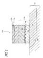
- FIG. 2is a schematic cross-section of the structure of FIG. 1 after patterning to define a programmable memory cell in a stud configuration.
- FIG. 3is a schematic cross-section of the programmable memory cell of FIG. 2 after deposition of a thin, conformal sealing layer.
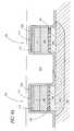
- FIG. 4Ais a schematic cross-section of two cells in an array of programmable memory cells, similar to that of FIG. 3 , after deposition of a layer of insulating material to fill the spaces around them.
- FIG. 4Bis a schematic cross-section of the cells of FIG. 4A after electrical contacts to the electrodes of the cells have been made.
- the preferred embodimentdiscloses a method of fabricating a programmable memory cell in a stud configuration. Blanket layers of electrode and body materials are deposited and subsequently patterned and etched, leaving pillars or studs as individual devices. The blanket deposition of the layers avoids problems associated with via filling and allows more flexibility in cell configuration.
- a semiconductor base material 100 containing a heavily doped (e.g., n + ) conductive region 102comprises the substrate 101 upon which the memory cells are fabricated.
- the substratecomprises the lowest layer of semiconductor material from which devices are formed in the integrated circuit.
- the substratecomprises a single-crystal silicon wafer.
- an epitaxial silicon layer or another semiconductor, such as a III-V material,can be used.
- a bottom electrode 103makes contact with the substrate.
- the bottom electrode 103can include more than one layer.
- the bottom electrode 103comprises a layer of polysilicon 104 , a layer of tungsten nitride 106 and a layer of tungsten 108 .
- the polysilicon layer 104is between about 25 nm and 75 nm thick
- the tungsten nitride layer 106is between about 5 nm and 40 nm thick
- the tungsten layer 108is between about 50 nm and 100 nm thick.
- the body 110 of the programmable memory cellis deposited over the electrode 103 .
- the memory cell body 110comprises a glass material, preferably a chalcogenide glass selected from the group consisting of sulfur, germanium, selenium and tellurium, more preferably a glass comprising germanium (Ge) and selenium (Se), in which the ratio of Ge:Se can vary (e.g., Ge 4 Se 6 , Ge 3 Se 7 or Ge 2 Se 8 ) but is preferably targeted for about Ge 25 Se 75 ).
- the thickness of the germanium selenide layeris preferably between about 25 nm and 75 nm, with a target thickness of about 50 nm in the illustrated embodiment.
- Preferred methods of depositing the Ge—Se materialinclude sputtering and evaporation. More complicated structures for the cell body are also contemplated, as discussed below.
- a metal film(not shown) is deposited over the memory cell body 110 as a source of metal ions for diffusion into the memory cell body.
- the metal filmincludes a metal from Group B or Group IIB (e.g., silver, copper or zinc), and more preferably the metal is silver.
- the metal filmmay be co-sputtered tungsten-silver.
- Energyis provided to diffuse metal from the film into the memory cell body 110 , preferably by photodissolution, a self-limiting reaction. Take, for example, a silver layer of 30 nm over a Ge—Se layer 110 of 50 nm, exposed to ultraviolet radiation, particularly ultraviolet radiation with a wavelength of less than 500 nm at about 4 mW/cm 2 for about 15 min.
- Sufficient silverdissolves into the glass layer 110 to saturate the glass by forming a glass electrolyte ternary compound with about 30 atomic percent silver. It is preferred that there be some silver film left over the cell body 110 after the diffusion occurs.
- the 50-nm layer of Ge—Seconsumes about 15 nm of silver, leaving a film 112 of about 15 nm over the memory cell body after the photodissolution reaction.
- metal for the programmable conductor memory cell bodyis supplied by other means.
- the metal and glass materialcan be co-sputtered or deposited from a source that contains all species, so no metal deposition and drive-in steps are needed.
- This fast ion conducting element with metal ions diffused thereinwill be referred to herein as the memory cell body 110 .
- the cell body 110can include multiple layers.
- the cell body 110in one embodiment includes a first Ge—Se layer (e.g., Ge 4 Se 6 ), a metal selenide layer (e.g., Ag 2 Se) thereover, and a second Ge—Se layer (e.g., Ge 4 Se 6 ) over the metal selenide layer.
- a first Ge—Se layere.g., Ge 4 Se 6
- a metal selenide layere.g., Ag 2 Se
- Ge 4 Se 6Ge 4 Se 6
- the intermediate metal selenide layerprovides metal to the cell body 110 for formation of conductive pathways under the influence of applied electrical fields.
- the top electrodefurther comprises a tungsten layer 114 with a thickness between about 5 nm and 25 nm and is formed over any remaining or added metal film 112 .
- the stack of blanket layersis patterned using a mask that forms pillars, preferably less than about 250 nm in width and preferably separated from one another by at least about 300 nm, using standard photolithographic techniques as are known in the art.
- the layers from the bottom electrode 103 to the top electrode 114are then etched down to the substrate 101 , preferably including a physical etch component, more preferably using Ar/Cl sputtering or reactive ion etching.
- each pillar 120is an individual programmable memory cell.
- the width of each cell 120is less than about 250 nm, and the spaces between the cells are at least about 300 nm in width.
- the skilled artisanwill readily appreciate that such spacing issues will depend upon the critical dimension for any particular generation of integrated circuit processing. Currently, state-of the-art fabrication techniques employ 0.13 ⁇ m line widths, although this critical dimension is expected to continue to shrink with each new generation of integrated circuit technology.
- FIG. 3shows an exemplary memory cell 120 , covered by a blanket liner layer 200 of insulating material, preferably between about 5 nm and 50 nm in thickness, and also preferably comprising a material that can serve as a diffusion barrier.
- the liner layer 200is selected to prevent diffusion of metal from metal film 112 away from the cell 120 and into other areas of the integrated circuit, where it could cause severe problems.
- the liner layer 200comprises silicon nitride that conforms over the cells and the semiconductor base material.
- Fabrication of the memory cell array of the illustrated embodimentcomprises deposition of a blanket layer of silver to a thickness of about 30 nm. Much of the blanket layer is removed during etching to form individual memory cell stacks 120 . The silver that remains in the individual cells is encapsulated by the liner layer 200 to prevent it from diffusing away from the cell 120 .
- FIG. 4Ashows two memory cells 120 in a memory array after blanket deposition of an insulating layer 210 to fill the spaces between the separate cells 120 .
- the insulating material 210is silicon oxide deposited using TEOS, although the skilled artisan will readily appreciate that other insulating materials (e.g., low k materials) known in the art can be used readily with good result.
- Electrodesare made to the electrodes of the memory cells 120 as shown in FIG. 4 B. At least some of the insulating material 210 and/or liner layer 200 are removed from the upper surface of electrode layer 114 . These materials can be removed by chemical mechanical polishing (CMP), arranged to stop on and expose the top surface of electrode layer 114 , or alternatively by patterning and etching, preferably dry etching, as shown in FIG. 4B , or any other method known in the art. Note that the drawings are not to scale and that the openings for making contact can be comparable to the dimensions of the cell 120 top surface. In addition, vias are etched through the insulating layer 210 between cells down to the conducting region 102 of the semiconductor substrate 101 . A conducting material is used to make contact to both the electrode layers 114 (contacts 220 ) and the conducting region 102 of the substrate (contacts 230 ). Contact 230 makes electrical connection to the lower electrode 103 through conducting region 102 .
- CMPchemical mechanical polishing
- a conducting materialis used to make
- the preferred embodimentthus involves an array of programmable conductor memory cells wherein each cell comprises stacked materials on a semiconductor substrate.
- the regions between the cellscomprise insulating material, preferably including a thin barrier layer 200 (preferably silicon nitride) conforming to the cells 120 and to the substrate 100 and a thick layer of insulation 210 (preferably a form of silicon oxide) that fills in the remaining space between the cells.
- the barrier layer 200is between about 5 nm and 50 nm thick.
- the silicon oxide 210is deposited from tetraethylorthosilicate (TEOS).
- Each programmable conductor memory cell 120comprises the layers discussed above in reference to FIGS. 1-4 . These include a bottom electrode 103 comprising one or more layers, a cell body 110 that includes glass electrolyte layer having metal ions diffused therein and a top electrode 112 , 114 .
- the bottom electrode 103preferably comprises a polysilicon layer 104 , a tungsten nitride layer 106 and a tungsten layer 108 .
- the polysilicon layer 104is between about 25 nm and 75 nm thick
- the tungsten nitride layer 106is between about 5 nm and 40 nm thick
- the tungsten layer 108is between about 50 nm and 100 nm thick.
- the glass electrolyte material 110comprises a chalcogenide glass with metal ions diffused therein, more preferably silver germanium selenide, typically of the form Ag/Ge 25 Se 75 .
- the thickness of the silver germanium selenide layeris preferably between about 25 nm and 75 nm. There is some silver film 112 remaining over the glass after silver ions have been driven into the Ge—Se, whether left over from photodissolution or deposited after forming the electrolyte 110 .
- the top electrodealso comprises a tungsten layer 114 over the silver film 112 with a thickness between about 5 nm and 25 nm.
- the memory cell body 110i.e., the glass electrolyte material having metal ions therein, forms conductive pathways that grow from the negative electrode to the positive electrode when a first voltage is applied to the electrodes 103 , 114 .
- the growth of the conductive pathwaysdepends upon applied voltage and time. Low voltages cause slow growth, whereas higher voltages result in faster growth of conductive path(s) from the negative electrode to the positive electrode. Without being limited by theory, it is believed that the conductive pathways grow by precipitation of cations (e.g., silver cations) from the memory cell body 110 . Changes in the extent of the conductive pathways affect the resistance of the devices. The conductive pathway remains intact when the voltage is removed.
- the memoryFor a binary programmable conductor memory device, the memory has two basic states: 0 and 1. When there is no conductive pathway, the memory cell has high electrical resistance and reads as 0. When the conductive pathway shorts the memory cell body, from the cathode to the anode, the resistance is low and the memory cell reads as 1.
- the change in resistance of the memory cell with and without a conductive pathwaycan be as much as two orders of magnitude, i.e., a change from Megaohms to milliohms. Reversing the polarity of the voltage preferably reverses the conductive pathway.
- the memory cellcan be programmed into as many as 3 or 4 states by setting the extent of the conductive pathway. These changes can be detected easily by passing current through the bit lines and word lines (not shown) connected to the contacts 220 , 230 in the memory array, such that changing the extent of the pathways can serve to change the state of the memory bit.
Landscapes
- Engineering & Computer Science (AREA)
- Manufacturing & Machinery (AREA)
- Semiconductor Memories (AREA)
Abstract
Description
Claims (27)
Priority Applications (4)
| Application Number | Priority Date | Filing Date | Title |
|---|---|---|---|
| US10/121,792US6858482B2 (en) | 2002-04-10 | 2002-04-10 | Method of manufacture of programmable switching circuits and memory cells employing a glass layer |
| PCT/US2003/010952WO2003088250A2 (en) | 2002-04-10 | 2003-04-10 | Method of manufacture of programmable conductor memory |
| AU2003231998AAU2003231998A1 (en) | 2002-04-10 | 2003-04-10 | Method of manufacture of programmable conductor memory |
| US10/790,816US7479650B2 (en) | 2002-04-10 | 2004-03-03 | Method of manufacture of programmable conductor memory |
Applications Claiming Priority (1)
| Application Number | Priority Date | Filing Date | Title |
|---|---|---|---|
| US10/121,792US6858482B2 (en) | 2002-04-10 | 2002-04-10 | Method of manufacture of programmable switching circuits and memory cells employing a glass layer |
Related Child Applications (1)
| Application Number | Title | Priority Date | Filing Date |
|---|---|---|---|
| US10/790,816DivisionUS7479650B2 (en) | 2002-04-10 | 2004-03-03 | Method of manufacture of programmable conductor memory |
Publications (2)
| Publication Number | Publication Date |
|---|---|
| US20030194865A1 US20030194865A1 (en) | 2003-10-16 |
| US6858482B2true US6858482B2 (en) | 2005-02-22 |
Family
ID=28790404
Family Applications (2)
| Application Number | Title | Priority Date | Filing Date |
|---|---|---|---|
| US10/121,792Expired - LifetimeUS6858482B2 (en) | 2002-04-10 | 2002-04-10 | Method of manufacture of programmable switching circuits and memory cells employing a glass layer |
| US10/790,816Expired - LifetimeUS7479650B2 (en) | 2002-04-10 | 2004-03-03 | Method of manufacture of programmable conductor memory |
Family Applications After (1)
| Application Number | Title | Priority Date | Filing Date |
|---|---|---|---|
| US10/790,816Expired - LifetimeUS7479650B2 (en) | 2002-04-10 | 2004-03-03 | Method of manufacture of programmable conductor memory |
Country Status (3)
| Country | Link |
|---|---|
| US (2) | US6858482B2 (en) |
| AU (1) | AU2003231998A1 (en) |
| WO (1) | WO2003088250A2 (en) |
Cited By (68)
| Publication number | Priority date | Publication date | Assignee | Title |
|---|---|---|---|---|
| US20050263823A1 (en)* | 2004-05-27 | 2005-12-01 | Young-Nam Hwang | Phase-change memory device having a barrier layer and manufacturing method |
| US20050263829A1 (en)* | 2004-05-27 | 2005-12-01 | Yoon-Jong Song | Semiconductor devices having phase change memory cells, electronic systems employing the same and methods of fabricating the same |
| US20060139989A1 (en)* | 2004-12-21 | 2006-06-29 | Infineon Technologies Ag | Integration of 1T1R CBRAM memory cells |
| US20070215987A1 (en)* | 2006-03-15 | 2007-09-20 | Schwerin Ulrike G | Method for forming a memory device and memory device |
| US20080314739A1 (en)* | 2007-06-19 | 2008-12-25 | International Business Machines Corporation | Electrolytic device based on a solution-processed electrolyte |
| US7825479B2 (en) | 2008-08-06 | 2010-11-02 | International Business Machines Corporation | Electrical antifuse having a multi-thickness dielectric layer |
| US8374018B2 (en) | 2010-07-09 | 2013-02-12 | Crossbar, Inc. | Resistive memory using SiGe material |
| US8391049B2 (en) | 2010-09-29 | 2013-03-05 | Crossbar, Inc. | Resistor structure for a non-volatile memory device and method |
| US8394670B2 (en) | 2011-05-31 | 2013-03-12 | Crossbar, Inc. | Vertical diodes for non-volatile memory device |
| US8404553B2 (en) | 2010-08-23 | 2013-03-26 | Crossbar, Inc. | Disturb-resistant non-volatile memory device and method |
| US8441835B2 (en) | 2010-06-11 | 2013-05-14 | Crossbar, Inc. | Interface control for improved switching in RRAM |
| US8450209B2 (en) | 2010-11-05 | 2013-05-28 | Crossbar, Inc. | p+ Polysilicon material on aluminum for non-volatile memory device and method |
| US8450710B2 (en) | 2011-05-27 | 2013-05-28 | Crossbar, Inc. | Low temperature p+ silicon junction material for a non-volatile memory device |
| US8467227B1 (en) | 2010-11-04 | 2013-06-18 | Crossbar, Inc. | Hetero resistive switching material layer in RRAM device and method |
| US8492195B2 (en) | 2010-08-23 | 2013-07-23 | Crossbar, Inc. | Method for forming stackable non-volatile resistive switching memory devices |
| US8519485B2 (en) | 2010-06-11 | 2013-08-27 | Crossbar, Inc. | Pillar structure for memory device and method |
| US8558212B2 (en) | 2010-09-29 | 2013-10-15 | Crossbar, Inc. | Conductive path in switching material in a resistive random access memory device and control |
| US8659929B2 (en) | 2011-06-30 | 2014-02-25 | Crossbar, Inc. | Amorphous silicon RRAM with non-linear device and operation |
| US8658476B1 (en) | 2012-04-20 | 2014-02-25 | Crossbar, Inc. | Low temperature P+ polycrystalline silicon material for non-volatile memory device |
| US8716098B1 (en) | 2012-03-09 | 2014-05-06 | Crossbar, Inc. | Selective removal method and structure of silver in resistive switching device for a non-volatile memory device |
| US8765566B2 (en) | 2012-05-10 | 2014-07-01 | Crossbar, Inc. | Line and space architecture for a non-volatile memory device |
| US8791010B1 (en) | 2010-12-31 | 2014-07-29 | Crossbar, Inc. | Silver interconnects for stacked non-volatile memory device and method |
| US8796658B1 (en) | 2012-05-07 | 2014-08-05 | Crossbar, Inc. | Filamentary based non-volatile resistive memory device and method |
| US8809831B2 (en) | 2010-07-13 | 2014-08-19 | Crossbar, Inc. | On/off ratio for non-volatile memory device and method |
| US8815696B1 (en) | 2010-12-31 | 2014-08-26 | Crossbar, Inc. | Disturb-resistant non-volatile memory device using via-fill and etchback technique |
| US8884261B2 (en) | 2010-08-23 | 2014-11-11 | Crossbar, Inc. | Device switching using layered device structure |
| US8889521B1 (en) | 2012-09-14 | 2014-11-18 | Crossbar, Inc. | Method for silver deposition for a non-volatile memory device |
| US8930174B2 (en) | 2010-12-28 | 2015-01-06 | Crossbar, Inc. | Modeling technique for resistive random access memory (RRAM) cells |
| US8934280B1 (en) | 2013-02-06 | 2015-01-13 | Crossbar, Inc. | Capacitive discharge programming for two-terminal memory cells |
| US8947908B2 (en) | 2010-11-04 | 2015-02-03 | Crossbar, Inc. | Hetero-switching layer in a RRAM device and method |
| US8946669B1 (en) | 2012-04-05 | 2015-02-03 | Crossbar, Inc. | Resistive memory device and fabrication methods |
| US8946673B1 (en) | 2012-08-24 | 2015-02-03 | Crossbar, Inc. | Resistive switching device structure with improved data retention for non-volatile memory device and method |
| US8946046B1 (en) | 2012-05-02 | 2015-02-03 | Crossbar, Inc. | Guided path for forming a conductive filament in RRAM |
| US8956939B2 (en) | 2013-04-29 | 2015-02-17 | Asm Ip Holding B.V. | Method of making a resistive random access memory device |
| US8982647B2 (en) | 2012-11-14 | 2015-03-17 | Crossbar, Inc. | Resistive random access memory equalization and sensing |
| US9006075B2 (en) | 2011-11-17 | 2015-04-14 | Micron Technology, Inc. | Memory cells, semiconductor devices including such cells, and methods of fabrication |
| US9012307B2 (en)* | 2010-07-13 | 2015-04-21 | Crossbar, Inc. | Two terminal resistive switching device structure and method of fabricating |
| US9087576B1 (en) | 2012-03-29 | 2015-07-21 | Crossbar, Inc. | Low temperature fabrication method for a three-dimensional memory device and structure |
| US9112145B1 (en) | 2013-01-31 | 2015-08-18 | Crossbar, Inc. | Rectified switching of two-terminal memory via real time filament formation |
| US9153623B1 (en) | 2010-12-31 | 2015-10-06 | Crossbar, Inc. | Thin film transistor steering element for a non-volatile memory device |
| US9191000B2 (en) | 2011-07-29 | 2015-11-17 | Crossbar, Inc. | Field programmable gate array utilizing two-terminal non-volatile memory |
| US9252191B2 (en) | 2011-07-22 | 2016-02-02 | Crossbar, Inc. | Seed layer for a p+ silicon germanium material for a non-volatile memory device and method |
| US9312483B2 (en) | 2012-09-24 | 2016-04-12 | Crossbar, Inc. | Electrode structure for a non-volatile memory device and method |
| US9324942B1 (en) | 2013-01-31 | 2016-04-26 | Crossbar, Inc. | Resistive memory cell with solid state diode |
| US9385164B2 (en) | 2013-04-29 | 2016-07-05 | Asm Ip Holding B.V. | Method of making a resistive random access memory device with metal-doped resistive switching layer |
| US9401475B1 (en) | 2010-08-23 | 2016-07-26 | Crossbar, Inc. | Method for silver deposition for a non-volatile memory device |
| US9406379B2 (en) | 2013-01-03 | 2016-08-02 | Crossbar, Inc. | Resistive random access memory with non-linear current-voltage relationship |
| US9412790B1 (en) | 2012-12-04 | 2016-08-09 | Crossbar, Inc. | Scalable RRAM device architecture for a non-volatile memory device and method |
| US9472757B2 (en) | 2013-07-19 | 2016-10-18 | Asm Ip Holding B.V. | Method of making a resistive random access memory device |
| US9520562B2 (en) | 2013-07-19 | 2016-12-13 | Asm Ip Holding B.V. | Method of making a resistive random access memory |
| US9543359B2 (en) | 2011-05-31 | 2017-01-10 | Crossbar, Inc. | Switching device having a non-linear element |
| US9564587B1 (en) | 2011-06-30 | 2017-02-07 | Crossbar, Inc. | Three-dimensional two-terminal memory with enhanced electric field and segmented interconnects |
| US9570678B1 (en) | 2010-06-08 | 2017-02-14 | Crossbar, Inc. | Resistive RAM with preferental filament formation region and methods |
| US9576616B2 (en) | 2012-10-10 | 2017-02-21 | Crossbar, Inc. | Non-volatile memory with overwrite capability and low write amplification |
| US9583701B1 (en) | 2012-08-14 | 2017-02-28 | Crossbar, Inc. | Methods for fabricating resistive memory device switching material using ion implantation |
| USRE46335E1 (en) | 2010-11-04 | 2017-03-07 | Crossbar, Inc. | Switching device having a non-linear element |
| US9601690B1 (en) | 2011-06-30 | 2017-03-21 | Crossbar, Inc. | Sub-oxide interface layer for two-terminal memory |
| US9601692B1 (en) | 2010-07-13 | 2017-03-21 | Crossbar, Inc. | Hetero-switching layer in a RRAM device and method |
| US9620206B2 (en) | 2011-05-31 | 2017-04-11 | Crossbar, Inc. | Memory array architecture with two-terminal memory cells |
| US9627443B2 (en) | 2011-06-30 | 2017-04-18 | Crossbar, Inc. | Three-dimensional oblique two-terminal memory with enhanced electric field |
| US9633723B2 (en) | 2011-06-23 | 2017-04-25 | Crossbar, Inc. | High operating speed resistive random access memory |
| US9685608B2 (en) | 2012-04-13 | 2017-06-20 | Crossbar, Inc. | Reduced diffusion in metal electrode for two-terminal memory |
| US9729155B2 (en) | 2011-07-29 | 2017-08-08 | Crossbar, Inc. | Field programmable gate array utilizing two-terminal non-volatile memory |
| US9735358B2 (en) | 2012-08-14 | 2017-08-15 | Crossbar, Inc. | Noble metal / non-noble metal electrode for RRAM applications |
| US9741765B1 (en) | 2012-08-14 | 2017-08-22 | Crossbar, Inc. | Monolithically integrated resistive memory using integrated-circuit foundry compatible processes |
| US10056907B1 (en) | 2011-07-29 | 2018-08-21 | Crossbar, Inc. | Field programmable gate array utilizing two-terminal non-volatile memory |
| US10290801B2 (en) | 2014-02-07 | 2019-05-14 | Crossbar, Inc. | Scalable silicon based resistive memory device |
| US11068620B2 (en) | 2012-11-09 | 2021-07-20 | Crossbar, Inc. | Secure circuit integrated with memory layer |
Families Citing this family (22)
| Publication number | Priority date | Publication date | Assignee | Title |
|---|---|---|---|---|
| US20040052117A1 (en)* | 2002-07-05 | 2004-03-18 | Hai Jiang | Fabrication of ultra-small memory elements |
| US6784069B1 (en)* | 2003-08-29 | 2004-08-31 | Micron Technology, Inc. | Permeable capacitor electrode |
| DE102004041894B3 (en)* | 2004-08-30 | 2006-03-09 | Infineon Technologies Ag | A memory device (CBRAM) having memory cells based on a resistance variable active solid electrolyte material and method of manufacturing the same |
| TW200620473A (en)* | 2004-09-08 | 2006-06-16 | Renesas Tech Corp | Nonvolatile memory device |
| US7937198B2 (en)* | 2004-12-29 | 2011-05-03 | Snap-On Incorporated | Vehicle or engine diagnostic systems supporting fast boot and reprogramming |
| US7634337B2 (en)* | 2004-12-29 | 2009-12-15 | Snap-On Incorporated | Vehicle or engine diagnostic systems with advanced non-volatile memory |
| US7214958B2 (en)* | 2005-02-10 | 2007-05-08 | Infineon Technologies Ag | Phase change memory cell with high read margin at low power operation |
| US7348590B2 (en)* | 2005-02-10 | 2008-03-25 | Infineon Technologies Ag | Phase change memory cell with high read margin at low power operation |
| US7361925B2 (en)* | 2005-02-10 | 2008-04-22 | Infineon Technologies Ag | Integrated circuit having a memory including a low-k dielectric material for thermal isolation |
| WO2006129367A1 (en)* | 2005-06-02 | 2006-12-07 | Misuzu R & D Ltd. | Nonvolatile memory |
| JP5175525B2 (en)* | 2007-11-14 | 2013-04-03 | 株式会社東芝 | Nonvolatile semiconductor memory device |
| KR100912822B1 (en) | 2007-11-22 | 2009-08-18 | 한국전자통신연구원 | Solid Electrolyte Memory Device and Manufacturing Method Thereof |
| JP5531296B2 (en)* | 2008-09-02 | 2014-06-25 | 株式会社東芝 | Nonvolatile semiconductor memory device |
| US8058646B2 (en) | 2008-10-29 | 2011-11-15 | Seagate Technology Llc | Programmable resistive memory cell with oxide layer |
| US9812638B2 (en)* | 2010-03-19 | 2017-11-07 | Globalfoundries Inc. | Backend of line (BEOL) compatible high current density access device for high density arrays of electronic components |
| FR2970115B1 (en)* | 2010-12-29 | 2013-01-18 | Altis Semiconductor Snc | METHOD FOR ETCHING A PROGRAMMABLE MEMORY MICROELECTRONIC DEVICE |
| US8487293B2 (en)* | 2010-12-30 | 2013-07-16 | Micron Technology, Inc. | Bipolar switching memory cell with built-in “on ”state rectifying current-voltage characteristics |
| US9048415B2 (en) | 2012-01-11 | 2015-06-02 | Micron Technology, Inc. | Memory cells including top electrodes comprising metal silicide, apparatuses including such cells, and related methods |
| US10483462B1 (en)* | 2015-06-17 | 2019-11-19 | Crossbar, Inc. | Formation of structurally robust nanoscale Ag-based conductive structure |
| TWI625874B (en)* | 2015-11-05 | 2018-06-01 | 華邦電子股份有限公司 | Conductive-bridging random access memory |
| US11289650B2 (en)* | 2019-03-04 | 2022-03-29 | International Business Machines Corporation | Stacked access device and resistive memory |
| US20210288250A1 (en)* | 2020-03-13 | 2021-09-16 | International Business Machines Corporation | Phase Change Memory Having Gradual Reset |
Citations (192)
| Publication number | Priority date | Publication date | Assignee | Title |
|---|---|---|---|---|
| US3271591A (en) | 1963-09-20 | 1966-09-06 | Energy Conversion Devices Inc | Symmetrical current controlling device |
| US3622319A (en) | 1966-10-20 | 1971-11-23 | Western Electric Co | Nonreflecting photomasks and methods of making same |
| US3743847A (en) | 1971-06-01 | 1973-07-03 | Motorola Inc | Amorphous silicon film as a uv filter |
| US3961314A (en) | 1974-03-05 | 1976-06-01 | Energy Conversion Devices, Inc. | Structure and method for producing an image |
| US3966317A (en) | 1974-04-08 | 1976-06-29 | Energy Conversion Devices, Inc. | Dry process production of archival microform records from hard copy |
| US3983542A (en) | 1970-08-13 | 1976-09-28 | Energy Conversion Devices, Inc. | Method and apparatus for recording information |
| US4177474A (en) | 1977-05-18 | 1979-12-04 | Energy Conversion Devices, Inc. | High temperature amorphous semiconductor member and method of making the same |
| US4267261A (en) | 1971-07-15 | 1981-05-12 | Energy Conversion Devices, Inc. | Method for full format imaging |
| US4269935A (en) | 1979-07-13 | 1981-05-26 | Ionomet Company, Inc. | Process of doping silver image in chalcogenide layer |
| JPS56126916A (en) | 1980-03-10 | 1981-10-05 | Nippon Telegr & Teleph Corp <Ntt> | Manufacture of semiconductor device |
| US4312938A (en) | 1979-07-06 | 1982-01-26 | Drexler Technology Corporation | Method for making a broadband reflective laser recording and data storage medium with absorptive underlayer |
| US4316946A (en) | 1979-12-03 | 1982-02-23 | Ionomet Company, Inc. | Surface sensitized chalcogenide product and process for making and using the same |
| US4320191A (en) | 1978-11-07 | 1982-03-16 | Nippon Telegraph & Telephone Public Corporation | Pattern-forming process |
| US4405710A (en) | 1981-06-22 | 1983-09-20 | Cornell Research Foundation, Inc. | Ion beam exposure of (g-Gex -Se1-x) inorganic resists |
| US4419421A (en) | 1979-01-15 | 1983-12-06 | Max-Planck-Gesellschaft Zur Forderung Der Wissenschaften E.V. | Ion conductor material |
| US4499557A (en) | 1980-10-28 | 1985-02-12 | Energy Conversion Devices, Inc. | Programmable cell for use in programmable electronic arrays |
| US4597162A (en) | 1983-01-18 | 1986-07-01 | Energy Conversion Devices, Inc. | Method for making, parallel preprogramming or field programming of electronic matrix arrays |
| US4608296A (en) | 1983-12-06 | 1986-08-26 | Energy Conversion Devices, Inc. | Superconducting films and devices exhibiting AC to DC conversion |
| US4637895A (en) | 1985-04-01 | 1987-01-20 | Energy Conversion Devices, Inc. | Gas mixtures for the vapor deposition of semiconductor material |
| US4646266A (en) | 1984-09-28 | 1987-02-24 | Energy Conversion Devices, Inc. | Programmable semiconductor structures and methods for using the same |
| US4664939A (en) | 1985-04-01 | 1987-05-12 | Energy Conversion Devices, Inc. | Vertical semiconductor processor |
| US4668968A (en) | 1984-05-14 | 1987-05-26 | Energy Conversion Devices, Inc. | Integrated circuit compatible thin film field effect transistor and method of making same |
| US4670763A (en) | 1984-05-14 | 1987-06-02 | Energy Conversion Devices, Inc. | Thin film field effect transistor |
| US4671618A (en) | 1986-05-22 | 1987-06-09 | Wu Bao Gang | Liquid crystalline-plastic material having submillisecond switch times and extended memory |
| US4673957A (en) | 1984-05-14 | 1987-06-16 | Energy Conversion Devices, Inc. | Integrated circuit compatible thin film field effect transistor and method of making same |
| US4678679A (en) | 1984-06-25 | 1987-07-07 | Energy Conversion Devices, Inc. | Continuous deposition of activated process gases |
| US4710899A (en) | 1985-06-10 | 1987-12-01 | Energy Conversion Devices, Inc. | Data storage medium incorporating a transition metal for increased switching speed |
| US4728406A (en) | 1986-08-18 | 1988-03-01 | Energy Conversion Devices, Inc. | Method for plasma - coating a semiconductor body |
| US4737379A (en) | 1982-09-24 | 1988-04-12 | Energy Conversion Devices, Inc. | Plasma deposited coatings, and low temperature plasma method of making same |
| US4766471A (en) | 1986-01-23 | 1988-08-23 | Energy Conversion Devices, Inc. | Thin film electro-optical devices |
| US4769338A (en) | 1984-05-14 | 1988-09-06 | Energy Conversion Devices, Inc. | Thin film field effect transistor and method of making same |
| US4775425A (en) | 1987-07-27 | 1988-10-04 | Energy Conversion Devices, Inc. | P and n-type microcrystalline semiconductor alloy material including band gap widening elements, devices utilizing same |
| US4788594A (en) | 1986-10-15 | 1988-11-29 | Energy Conversion Devices, Inc. | Solid state electronic camera including thin film matrix of photosensors |
| US4795657A (en) | 1984-04-13 | 1989-01-03 | Energy Conversion Devices, Inc. | Method of fabricating a programmable array |
| US4800526A (en) | 1987-05-08 | 1989-01-24 | Gaf Corporation | Memory element for information storage and retrieval system and associated process |
| US4804490A (en) | 1987-10-13 | 1989-02-14 | Energy Conversion Devices, Inc. | Method of fabricating stabilized threshold switching material |
| US4809044A (en) | 1986-08-22 | 1989-02-28 | Energy Conversion Devices, Inc. | Thin film overvoltage protection devices |
| US4818717A (en) | 1986-06-27 | 1989-04-04 | Energy Conversion Devices, Inc. | Method for making electronic matrix arrays |
| US4843443A (en) | 1984-05-14 | 1989-06-27 | Energy Conversion Devices, Inc. | Thin film field effect transistor and method of making same |
| US4845533A (en) | 1986-08-22 | 1989-07-04 | Energy Conversion Devices, Inc. | Thin film electrical devices with amorphous carbon electrodes and method of making same |
| US4847674A (en) | 1987-03-10 | 1989-07-11 | Advanced Micro Devices, Inc. | High speed interconnect system with refractory non-dogbone contacts and an active electromigration suppression mechanism |
| US4853785A (en) | 1986-10-15 | 1989-08-01 | Energy Conversion Devices, Inc. | Electronic camera including electronic signal storage cartridge |
| US4891330A (en) | 1987-07-27 | 1990-01-02 | Energy Conversion Devices, Inc. | Method of fabricating n-type and p-type microcrystalline semiconductor alloy material including band gap widening elements |
| US4920078A (en) | 1989-06-02 | 1990-04-24 | Bell Communications Research, Inc. | Arsenic sulfide surface passivation of III-V semiconductors |
| US5128099A (en) | 1991-02-15 | 1992-07-07 | Energy Conversion Devices, Inc. | Congruent state changeable optical memory material and device |
| US5159661A (en) | 1990-10-05 | 1992-10-27 | Energy Conversion Devices, Inc. | Vertically interconnected parallel distributed processor |
| US5166758A (en) | 1991-01-18 | 1992-11-24 | Energy Conversion Devices, Inc. | Electrically erasable phase change memory |
| US5177567A (en) | 1991-07-19 | 1993-01-05 | Energy Conversion Devices, Inc. | Thin-film structure for chalcogenide electrical switching devices and process therefor |
| US5219788A (en) | 1991-02-25 | 1993-06-15 | Ibm Corporation | Bilayer metallization cap for photolithography |
| US5238862A (en) | 1992-03-18 | 1993-08-24 | Micron Technology, Inc. | Method of forming a stacked capacitor with striated electrode |
| US5272359A (en) | 1988-04-07 | 1993-12-21 | California Institute Of Technology | Reversible non-volatile switch based on a TCNQ charge transfer complex |
| US5296716A (en) | 1991-01-18 | 1994-03-22 | Energy Conversion Devices, Inc. | Electrically erasable, directly overwritable, multibit single cell memory elements and arrays fabricated therefrom |
| US5314772A (en) | 1990-10-09 | 1994-05-24 | Arizona Board Of Regents | High resolution, multi-layer resist for microlithography and method therefor |
| US5315131A (en) | 1990-11-22 | 1994-05-24 | Matsushita Electric Industrial Co., Ltd. | Electrically reprogrammable nonvolatile memory device |
| US5330630A (en) | 1991-01-02 | 1994-07-19 | Energy Conversion Devices, Inc. | Switch with improved threshold voltage |
| US5335219A (en) | 1991-01-18 | 1994-08-02 | Ovshinsky Stanford R | Homogeneous composition of microcrystalline semiconductor material, semiconductor devices and directly overwritable memory elements fabricated therefrom, and arrays fabricated from the memory elements |
| US5341328A (en) | 1991-01-18 | 1994-08-23 | Energy Conversion Devices, Inc. | Electrically erasable memory elements having reduced switching current requirements and increased write/erase cycle life |
| US5350484A (en) | 1992-09-08 | 1994-09-27 | Intel Corporation | Method for the anisotropic etching of metal films in the fabrication of interconnects |
| US5359205A (en) | 1991-11-07 | 1994-10-25 | Energy Conversion Devices, Inc. | Electrically erasable memory elements characterized by reduced current and improved thermal stability |
| US5360981A (en) | 1989-05-11 | 1994-11-01 | British Telecommunications Public Limited Company | Amorphous silicon memory |
| US5406509A (en) | 1991-01-18 | 1995-04-11 | Energy Conversion Devices, Inc. | Electrically erasable, directly overwritable, multibit single cell memory elements and arrays fabricated therefrom |
| US5414271A (en) | 1991-01-18 | 1995-05-09 | Energy Conversion Devices, Inc. | Electrically erasable memory elements having improved set resistance stability |
| US5500532A (en) | 1994-08-18 | 1996-03-19 | Arizona Board Of Regents | Personal electronic dosimeter |
| US5512773A (en) | 1993-12-23 | 1996-04-30 | U.S. Philips Corporation | Switching element with memory provided with Schottky tunnelling barrier |
| US5512328A (en) | 1992-08-07 | 1996-04-30 | Hitachi, Ltd. | Method for forming a pattern and forming a thin film used in pattern formation |
| US5534711A (en) | 1991-01-18 | 1996-07-09 | Energy Conversion Devices, Inc. | Electrically erasable, directly overwritable, multibit single cell memory elements and arrays fabricated therefrom |
| US5534712A (en) | 1991-01-18 | 1996-07-09 | Energy Conversion Devices, Inc. | Electrically erasable memory elements characterized by reduced current and improved thermal stability |
| US5536947A (en) | 1991-01-18 | 1996-07-16 | Energy Conversion Devices, Inc. | Electrically erasable, directly overwritable, multibit single cell memory element and arrays fabricated therefrom |
| US5543737A (en) | 1995-02-10 | 1996-08-06 | Energy Conversion Devices, Inc. | Logical operation circuit employing two-terminal chalcogenide switches |
| US5591501A (en) | 1995-12-20 | 1997-01-07 | Energy Conversion Devices, Inc. | Optical recording medium having a plurality of discrete phase change data recording points |
| US5596522A (en) | 1991-01-18 | 1997-01-21 | Energy Conversion Devices, Inc. | Homogeneous compositions of microcrystalline semiconductor material, semiconductor devices and directly overwritable memory elements fabricated therefrom, and arrays fabricated from the memory elements |
| US5687112A (en) | 1996-04-19 | 1997-11-11 | Energy Conversion Devices, Inc. | Multibit single cell memory element having tapered contact |
| US5694054A (en) | 1995-11-28 | 1997-12-02 | Energy Conversion Devices, Inc. | Integrated drivers for flat panel displays employing chalcogenide logic elements |
| US5714768A (en) | 1995-10-24 | 1998-02-03 | Energy Conversion Devices, Inc. | Second-layer phase change memory array on top of a logic device |
| US5726083A (en) | 1994-11-29 | 1998-03-10 | Nec Corporation | Process of fabricating dynamic random access memory device having storage capacitor low in contact resistance and small in leakage current through tantalum oxide film |
| US5751012A (en) | 1995-06-07 | 1998-05-12 | Micron Technology, Inc. | Polysilicon pillar diode for use in a non-volatile memory cell |
| US5761115A (en) | 1996-05-30 | 1998-06-02 | Axon Technologies Corporation | Programmable metallization cell structure and method of making same |
| US5789277A (en) | 1996-07-22 | 1998-08-04 | Micron Technology, Inc. | Method of making chalogenide memory device |
| US5814527A (en) | 1996-07-22 | 1998-09-29 | Micron Technology, Inc. | Method of making small pores defined by a disposable internal spacer for use in chalcogenide memories |
| US5818749A (en) | 1993-08-20 | 1998-10-06 | Micron Technology, Inc. | Integrated circuit memory device |
| US5825046A (en) | 1996-10-28 | 1998-10-20 | Energy Conversion Devices, Inc. | Composite memory material comprising a mixture of phase-change memory material and dielectric material |
| US5837564A (en) | 1995-11-01 | 1998-11-17 | Micron Technology, Inc. | Method for optimal crystallization to obtain high electrical performance from chalcogenides |
| US5841150A (en) | 1995-06-07 | 1998-11-24 | Micron Technology, Inc. | Stack/trench diode for use with a muti-state material in a non-volatile memory cell |
| US5846889A (en) | 1997-03-14 | 1998-12-08 | The United States Of America As Represented By The Secretary Of The Navy | Infrared transparent selenide glasses |
| US5851882A (en) | 1996-05-06 | 1998-12-22 | Micron Technology, Inc. | ZPROM manufacture and design and methods for forming thin structures using spacers as an etching mask |
| US5869843A (en) | 1995-06-07 | 1999-02-09 | Micron Technology, Inc. | Memory array having a multi-state element and method for forming such array or cells thereof |
| WO1999028914A2 (en) | 1997-12-04 | 1999-06-10 | Axon Technologies Corporation | Programmable sub-surface aggregating metallization structure and method of making same |
| US5912839A (en) | 1998-06-23 | 1999-06-15 | Energy Conversion Devices, Inc. | Universal memory element and method of programming same |
| US5920788A (en) | 1995-06-07 | 1999-07-06 | Micron Technology, Inc. | Chalcogenide memory cell with a plurality of chalcogenide electrodes |
| US5933365A (en) | 1997-06-19 | 1999-08-03 | Energy Conversion Devices, Inc. | Memory element with energy control mechanism |
| US5976928A (en)* | 1997-11-20 | 1999-11-02 | Advanced Technology Materials, Inc. | Chemical mechanical polishing of FeRAM capacitors |
| US5998066A (en) | 1997-05-16 | 1999-12-07 | Aerial Imaging Corporation | Gray scale mask and depth pattern transfer technique using inorganic chalcogenide glass |
| US6011757A (en) | 1998-01-27 | 2000-01-04 | Ovshinsky; Stanford R. | Optical recording media having increased erasability |
| US6031287A (en) | 1997-06-18 | 2000-02-29 | Micron Technology, Inc. | Contact structure and memory element incorporating the same |
| US6072716A (en) | 1999-04-14 | 2000-06-06 | Massachusetts Institute Of Technology | Memory structures and methods of making same |
| US6087674A (en) | 1996-10-28 | 2000-07-11 | Energy Conversion Devices, Inc. | Memory element with memory material comprising phase-change material and dielectric material |
| US6117720A (en) | 1995-06-07 | 2000-09-12 | Micron Technology, Inc. | Method of making an integrated circuit electrode having a reduced contact area |
| US6141241A (en) | 1998-06-23 | 2000-10-31 | Energy Conversion Devices, Inc. | Universal memory element with systems employing same and apparatus and method for reading, writing and programming same |
| US6143604A (en) | 1999-06-04 | 2000-11-07 | Taiwan Semiconductor Manufacturing Company | Method for fabricating small-size two-step contacts for word-line strapping on dynamic random access memory (DRAM) |
| US6177338B1 (en) | 1999-02-08 | 2001-01-23 | Taiwan Semiconductor Manufacturing Company | Two step barrier process |
| US6236059B1 (en) | 1996-08-22 | 2001-05-22 | Micron Technology, Inc. | Memory cell incorporating a chalcogenide element and method of making same |
| US6297170B1 (en) | 1998-06-23 | 2001-10-02 | Vlsi Technology, Inc. | Sacrificial multilayer anti-reflective coating for mos gate formation |
| US6300684B1 (en) | 1995-06-07 | 2001-10-09 | Micron Technology, Inc. | Method for fabricating an array of ultra-small pores for chalcogenide memory cells |
| WO2000048196A9 (en) | 1999-02-11 | 2001-11-01 | Univ Arizona | Programmable microelectronic devices and methods of forming and programming same |
| US6329606B1 (en) | 1996-04-24 | 2001-12-11 | Amkor Technology, Inc. | Grid array assembly of circuit boards with singulation grooves |
| US20020000666A1 (en) | 1998-08-31 | 2002-01-03 | Michael N. Kozicki | Self-repairing interconnections for electrical circuits |
| US6339544B1 (en) | 2000-09-29 | 2002-01-15 | Intel Corporation | Method to enhance performance of thermal resistor device |
| US6348365B1 (en) | 2001-03-02 | 2002-02-19 | Micron Technology, Inc. | PCRAM cell manufacturing |
| US6350679B1 (en) | 1999-08-03 | 2002-02-26 | Micron Technology, Inc. | Methods of providing an interlevel dielectric layer intermediate different elevation conductive metal layers in the fabrication of integrated circuitry |
| US20020031005A1 (en)* | 2000-08-22 | 2002-03-14 | Seiko Epson Corporation | Memory cell array having ferroelectric capacitors, method of fabricating the same, and ferroelectric memory device |
| WO2002021542A1 (en) | 2000-09-08 | 2002-03-14 | Axon Technologies Corporation | Microelectronic programmable device and methods of forming and programming the same |
| US6376284B1 (en) | 1996-02-23 | 2002-04-23 | Micron Technology, Inc. | Method of fabricating a memory device |
| US6404665B1 (en) | 2000-09-29 | 2002-06-11 | Intel Corporation | Compositionally modified resistive electrode |
| US20020072188A1 (en) | 2000-12-08 | 2002-06-13 | Gilton Terry L. | Non-volatile resistance variable devices and method of forming same, analog memory devices and method of forming same, programmable memory cell and method of forming same, and method of structurally changing a non-volatile device |
| US6414376B1 (en) | 1997-07-31 | 2002-07-02 | Micron Technology, Inc. | Method and apparatus for reducing isolation stress in integrated circuits |
| US6423628B1 (en) | 1999-10-22 | 2002-07-23 | Lsi Logic Corporation | Method of forming integrated circuit structure having low dielectric constant material and having silicon oxynitride caps over closely spaced apart metal lines |
| US6429064B1 (en) | 2000-09-29 | 2002-08-06 | Intel Corporation | Reduced contact area of sidewall conductor |
| US20020106849A1 (en) | 2001-02-08 | 2002-08-08 | Moore John T. | Method of forming non-volatile resistance variable devices, method of precluding diffusion of a metal into adjacent chalcogenide material, and non-volatile resistance variable devices |
| US6437383B1 (en) | 2000-12-21 | 2002-08-20 | Intel Corporation | Dual trench isolation for a phase-change memory cell and method of making same |
| US6440837B1 (en) | 2000-07-14 | 2002-08-27 | Micron Technology, Inc. | Method of forming a contact structure in a semiconductor device |
| US20020123248A1 (en) | 2001-03-01 | 2002-09-05 | Moore John T. | Methods of metal doping a chalcogenide material |
| US20020127886A1 (en) | 2001-03-07 | 2002-09-12 | Moore John T. | Method to manufacture a buried electrode PCRAM cell |
| US20020132417A1 (en) | 2001-03-15 | 2002-09-19 | Jiutao Li | Agglomeration elimination for metal sputter deposition of chalcogenides |
| US6462984B1 (en) | 2001-06-29 | 2002-10-08 | Intel Corporation | Biasing scheme of floating unselected wordlines and bitlines of a diode-based memory array |
| US6469364B1 (en) | 1998-08-31 | 2002-10-22 | Arizona Board Of Regents | Programmable interconnection system for electrical circuits |
| US6473332B1 (en) | 2001-04-04 | 2002-10-29 | The University Of Houston System | Electrically variable multi-state resistance computing |
| US20020160551A1 (en) | 2001-03-15 | 2002-10-31 | Harshfield Steven T. | Memory elements and methods for making same |
| US20020163828A1 (en) | 2001-05-07 | 2002-11-07 | Coatue Corporation | Memory device with a self-assembled polymer film and method of making the same |
| US6480438B1 (en) | 2001-06-12 | 2002-11-12 | Ovonyx, Inc. | Providing equal cell programming conditions across a large and high density array of phase-change memory cells |
| US20020168820A1 (en) | 2000-09-08 | 2002-11-14 | Kozicki Michael N. | Microelectronic programmable device and methods of forming and programming the same |
| US20020168852A1 (en) | 2001-05-11 | 2002-11-14 | Harshfield Steven T. | PCRAM memory cell and method of making same |
| US6487113B1 (en) | 2001-06-29 | 2002-11-26 | Ovonyx, Inc. | Programming a phase-change memory with slow quench time |
| US6487106B1 (en) | 1999-01-12 | 2002-11-26 | Arizona Board Of Regents | Programmable microelectronic devices and method of forming and programming same |
| US6501111B1 (en) | 2000-06-30 | 2002-12-31 | Intel Corporation | Three-dimensional (3D) programmable device |
| US6507061B1 (en) | 2001-08-31 | 2003-01-14 | Intel Corporation | Multiple layer phase-change memory |
| US6512241B1 (en) | 2001-12-31 | 2003-01-28 | Intel Corporation | Phase change material memory device |
| US6511867B2 (en) | 2001-06-30 | 2003-01-28 | Ovonyx, Inc. | Utilizing atomic layer deposition for programmable device |
| US6511862B2 (en) | 2001-06-30 | 2003-01-28 | Ovonyx, Inc. | Modified contact for programmable devices |
| US6514805B2 (en) | 2001-06-30 | 2003-02-04 | Intel Corporation | Trench sidewall profile for device isolation |
| US20030027416A1 (en) | 2001-08-01 | 2003-02-06 | Moore John T. | Method of forming integrated circuitry, method of forming memory circuitry, and method of forming random access memory circuitry |
| US6518636B2 (en)* | 2000-01-20 | 2003-02-11 | Matsushita Electric Industrial Co., Ltd. | Semiconductor MISFET |
| US20030035315A1 (en) | 2001-04-06 | 2003-02-20 | Kozicki Michael N. | Microelectronic device, structure, and system, including a memory structure having a variable programmable property and method of forming the same |
| US20030038301A1 (en) | 2001-08-27 | 2003-02-27 | John Moore | Apparatus and method for dual cell common electrode PCRAM memory device |
| US20030045054A1 (en) | 2001-08-29 | 2003-03-06 | Campbell Kristy A. | Method of forming non-volatile resistance variable devices, method of forming a programmable memory cell of memory circuitry, and a non-volatile resistance variable device |
| US20030045049A1 (en) | 2001-08-29 | 2003-03-06 | Campbell Kristy A. | Method of forming chalcogenide comprising devices |
| US20030043631A1 (en) | 2001-08-30 | 2003-03-06 | Gilton Terry L. | Method of retaining memory state in a programmable conductor RAM |
| US6531373B2 (en) | 2000-12-27 | 2003-03-11 | Ovonyx, Inc. | Method of forming a phase-change memory cell using silicon on insulator low electrode in charcogenide elements |
| US20030049912A1 (en) | 2001-08-29 | 2003-03-13 | Campbell Kristy A. | Method of forming chalcogenide comprsing devices and method of forming a programmable memory cell of memory circuitry |
| US20030048519A1 (en) | 2000-02-11 | 2003-03-13 | Kozicki Michael N. | Microelectronic photonic structure and device and method of forming the same |
| US20030048744A1 (en) | 2001-09-01 | 2003-03-13 | Ovshinsky Stanford R. | Increased data storage in optical data storage and retrieval systems using blue lasers and/or plasmon lenses |
| US20030047765A1 (en) | 2001-08-30 | 2003-03-13 | Campbell Kristy A. | Stoichiometry for chalcogenide glasses useful for memory devices and method of formation |
| US6534781B2 (en) | 2000-12-26 | 2003-03-18 | Ovonyx, Inc. | Phase-change memory bipolar array utilizing a single shallow trench isolation for creating an individual active area region for two memory array elements and one bipolar base contact |
| US20030052330A1 (en)* | 2001-09-20 | 2003-03-20 | Klein Rita J. | Electro-and electroless plating of metal in the manufacture of PCRAM devices |
| US6545907B1 (en) | 2001-10-30 | 2003-04-08 | Ovonyx, Inc. | Technique and apparatus for performing write operations to a phase change material memory device |
| US6545287B2 (en) | 2001-09-07 | 2003-04-08 | Intel Corporation | Using selective deposition to form phase-change memory cells |
| US20030068862A1 (en) | 2001-08-30 | 2003-04-10 | Jiutao Li | Integrated circuit device and fabrication using metal-doped chalcogenide materials |
| US6555860B2 (en) | 2000-09-29 | 2003-04-29 | Intel Corporation | Compositionally modified resistive electrode |
| US6563164B2 (en) | 2000-09-29 | 2003-05-13 | Ovonyx, Inc. | Compositionally modified resistive electrode |
| US6567293B1 (en) | 2000-09-29 | 2003-05-20 | Ovonyx, Inc. | Single level metal memory cell using chalcogenide cladding |
| US6566700B2 (en) | 2001-10-11 | 2003-05-20 | Ovonyx, Inc. | Carbon-containing interfacial layer for phase-change memory |
| US20030095426A1 (en) | 2001-11-20 | 2003-05-22 | Glen Hush | Complementary bit PCRAM sense amplifier and method of operation |
| US20030096497A1 (en) | 2001-11-19 | 2003-05-22 | Micron Technology, Inc. | Electrode structure for use in an integrated circuit |
| US6570784B2 (en) | 2001-06-29 | 2003-05-27 | Ovonyx, Inc. | Programming a phase-change material memory |
| US6569705B2 (en) | 2000-12-21 | 2003-05-27 | Intel Corporation | Metal structure for a phase-change memory device |
| US6576921B2 (en) | 2001-11-08 | 2003-06-10 | Intel Corporation | Isolating phase change material memory cells |
| US20030107105A1 (en) | 1999-08-31 | 2003-06-12 | Kozicki Michael N. | Programmable chip-to-substrate interconnect structure and device and method of forming same |
| US20030117831A1 (en) | 2001-12-20 | 2003-06-26 | Glen Hush | Programmable conductor random access memory and a method for writing thereto |
| US6586761B2 (en) | 2001-09-07 | 2003-07-01 | Intel Corporation | Phase change material memory device |
| US6589714B2 (en) | 2001-06-26 | 2003-07-08 | Ovonyx, Inc. | Method for making programmable resistance memory element using silylated photoresist |
| US6590807B2 (en) | 2001-08-02 | 2003-07-08 | Intel Corporation | Method for reading a structural phase-change memory |
| US20030128612A1 (en) | 2002-01-04 | 2003-07-10 | John Moore | PCRAM rewrite prevention |
| US20030137869A1 (en) | 1998-12-04 | 2003-07-24 | Kozicki Michael N. | Programmable microelectronic device, structure, and system and method of forming the same |
| US20030143782A1 (en) | 2002-01-31 | 2003-07-31 | Gilton Terry L. | Methods of forming germanium selenide comprising devices and methods of forming silver selenide comprising structures |
| US6605527B2 (en) | 2001-06-30 | 2003-08-12 | Intel Corporation | Reduced area intersection between electrode and programming element |
| US20030156463A1 (en) | 2002-02-19 | 2003-08-21 | Casper Stephen L. | Programmable conductor random access memory and method for sensing same |
| US20030155589A1 (en) | 2002-02-20 | 2003-08-21 | Campbell Kristy A. | Silver-selenide/chalcogenide glass stack for resistance variable memory |
| US20030156447A1 (en) | 2000-02-11 | 2003-08-21 | Kozicki Michael N. | Programming circuit for a programmable microelectronic device, system including the circuit, and method of forming the same |
| US20030155606A1 (en) | 2002-02-15 | 2003-08-21 | Campbell Kristy A. | Method to alter chalcogenide glass for improved switching characteristics |
| US6613604B2 (en) | 2001-08-02 | 2003-09-02 | Ovonyx, Inc. | Method for making small pore for use in programmable resistance memory element |
| US6625054B2 (en) | 2001-12-28 | 2003-09-23 | Intel Corporation | Method and apparatus to program a phase change memory |
| US6642102B2 (en) | 2001-06-30 | 2003-11-04 | Intel Corporation | Barrier material encapsulation of programmable material |
| US6646297B2 (en) | 2000-12-26 | 2003-11-11 | Ovonyx, Inc. | Lower electrode isolation in a double-wide trench |
| US20030212725A1 (en) | 2002-05-10 | 2003-11-13 | Ovshinsky Stanford R. | Methods of factoring and modular arithmetic |
| US20030209971A1 (en) | 2000-02-11 | 2003-11-13 | Kozicki Michael N. | Programmable structure, an array including the structure, and methods of forming the same |
| US20030210564A1 (en) | 2001-10-26 | 2003-11-13 | Kozicki Michael N. | Tunable cantilever apparatus and method for making same |
| US6649928B2 (en) | 2000-12-13 | 2003-11-18 | Intel Corporation | Method to selectively remove one side of a conductive bottom electrode of a phase-change memory cell and structure obtained thereby |
| US6667900B2 (en) | 2001-12-28 | 2003-12-23 | Ovonyx, Inc. | Method and apparatus to operate a memory cell |
| US6673700B2 (en) | 2001-06-30 | 2004-01-06 | Ovonyx, Inc. | Reduced area intersection between electrode and programming element |
| US6687427B2 (en) | 2000-12-29 | 2004-02-03 | Intel Corporation | Optic switch |
| US6690026B2 (en) | 2001-09-28 | 2004-02-10 | Intel Corporation | Method of fabricating a three-dimensional array of active media |
| US6696355B2 (en) | 2000-12-14 | 2004-02-24 | Ovonyx, Inc. | Method to selectively increase the top resistance of the lower programming electrode in a phase-change memory |
| US20040035401A1 (en) | 2002-08-26 | 2004-02-26 | Subramanian Ramachandran | Hydrogen powered scooter |
Family Cites Families (5)
| Publication number | Priority date | Publication date | Assignee | Title |
|---|---|---|---|---|
| US5341271A (en)* | 1992-06-22 | 1994-08-23 | Minnesota Mining And Manufacturing Company | Surge arrester fault indicator |
| US5363329A (en)* | 1993-11-10 | 1994-11-08 | Eugeniy Troyan | Semiconductor memory device for use in an electrically alterable read-only memory |
| US6515343B1 (en)* | 1998-11-19 | 2003-02-04 | Quicklogic Corporation | Metal-to-metal antifuse with non-conductive diffusion barrier |
| JP2000328989A (en)* | 1999-05-18 | 2000-11-28 | Aisan Ind Co Ltd | Engine fuel injection control device |
| JP2001167595A (en)* | 1999-12-08 | 2001-06-22 | Mitsubishi Electric Corp | Semiconductor storage device |
- 2002
- 2002-04-10USUS10/121,792patent/US6858482B2/ennot_activeExpired - Lifetime
- 2003
- 2003-04-10AUAU2003231998Apatent/AU2003231998A1/ennot_activeWithdrawn
- 2003-04-10WOPCT/US2003/010952patent/WO2003088250A2/ennot_activeApplication Discontinuation
- 2004
- 2004-03-03USUS10/790,816patent/US7479650B2/ennot_activeExpired - Lifetime
Patent Citations (227)
| Publication number | Priority date | Publication date | Assignee | Title |
|---|---|---|---|---|
| US3271591A (en) | 1963-09-20 | 1966-09-06 | Energy Conversion Devices Inc | Symmetrical current controlling device |
| US3622319A (en) | 1966-10-20 | 1971-11-23 | Western Electric Co | Nonreflecting photomasks and methods of making same |
| US3988720A (en) | 1970-08-13 | 1976-10-26 | Energy Conversion Devices, Inc. | Recording and retrieving information in an amorphous memory material using a catalytic material |
| US3983542A (en) | 1970-08-13 | 1976-09-28 | Energy Conversion Devices, Inc. | Method and apparatus for recording information |
| US3743847A (en) | 1971-06-01 | 1973-07-03 | Motorola Inc | Amorphous silicon film as a uv filter |
| US4267261A (en) | 1971-07-15 | 1981-05-12 | Energy Conversion Devices, Inc. | Method for full format imaging |
| US3961314A (en) | 1974-03-05 | 1976-06-01 | Energy Conversion Devices, Inc. | Structure and method for producing an image |
| US3966317A (en) | 1974-04-08 | 1976-06-29 | Energy Conversion Devices, Inc. | Dry process production of archival microform records from hard copy |
| US4177474A (en) | 1977-05-18 | 1979-12-04 | Energy Conversion Devices, Inc. | High temperature amorphous semiconductor member and method of making the same |
| US4320191A (en) | 1978-11-07 | 1982-03-16 | Nippon Telegraph & Telephone Public Corporation | Pattern-forming process |
| US4419421A (en) | 1979-01-15 | 1983-12-06 | Max-Planck-Gesellschaft Zur Forderung Der Wissenschaften E.V. | Ion conductor material |
| US4312938A (en) | 1979-07-06 | 1982-01-26 | Drexler Technology Corporation | Method for making a broadband reflective laser recording and data storage medium with absorptive underlayer |
| US4269935A (en) | 1979-07-13 | 1981-05-26 | Ionomet Company, Inc. | Process of doping silver image in chalcogenide layer |
| US4316946A (en) | 1979-12-03 | 1982-02-23 | Ionomet Company, Inc. | Surface sensitized chalcogenide product and process for making and using the same |
| JPS56126916A (en) | 1980-03-10 | 1981-10-05 | Nippon Telegr & Teleph Corp <Ntt> | Manufacture of semiconductor device |
| US4499557A (en) | 1980-10-28 | 1985-02-12 | Energy Conversion Devices, Inc. | Programmable cell for use in programmable electronic arrays |
| US4405710A (en) | 1981-06-22 | 1983-09-20 | Cornell Research Foundation, Inc. | Ion beam exposure of (g-Gex -Se1-x) inorganic resists |
| US4737379A (en) | 1982-09-24 | 1988-04-12 | Energy Conversion Devices, Inc. | Plasma deposited coatings, and low temperature plasma method of making same |
| US4597162A (en) | 1983-01-18 | 1986-07-01 | Energy Conversion Devices, Inc. | Method for making, parallel preprogramming or field programming of electronic matrix arrays |
| US4608296A (en) | 1983-12-06 | 1986-08-26 | Energy Conversion Devices, Inc. | Superconducting films and devices exhibiting AC to DC conversion |
| US4795657A (en) | 1984-04-13 | 1989-01-03 | Energy Conversion Devices, Inc. | Method of fabricating a programmable array |
| US4843443A (en) | 1984-05-14 | 1989-06-27 | Energy Conversion Devices, Inc. | Thin film field effect transistor and method of making same |
| US4668968A (en) | 1984-05-14 | 1987-05-26 | Energy Conversion Devices, Inc. | Integrated circuit compatible thin film field effect transistor and method of making same |
| US4670763A (en) | 1984-05-14 | 1987-06-02 | Energy Conversion Devices, Inc. | Thin film field effect transistor |
| US4769338A (en) | 1984-05-14 | 1988-09-06 | Energy Conversion Devices, Inc. | Thin film field effect transistor and method of making same |
| US4673957A (en) | 1984-05-14 | 1987-06-16 | Energy Conversion Devices, Inc. | Integrated circuit compatible thin film field effect transistor and method of making same |
| US4678679A (en) | 1984-06-25 | 1987-07-07 | Energy Conversion Devices, Inc. | Continuous deposition of activated process gases |
| US4646266A (en) | 1984-09-28 | 1987-02-24 | Energy Conversion Devices, Inc. | Programmable semiconductor structures and methods for using the same |
| US4696758A (en) | 1985-04-01 | 1987-09-29 | Energy Conversion Devices, Inc. | Gas mixtures for the vapor deposition of semiconductor material |
| US4698234A (en) | 1985-04-01 | 1987-10-06 | Energy Conversion Devices, Inc. | Vapor deposition of semiconductor material |
| US4637895A (en) | 1985-04-01 | 1987-01-20 | Energy Conversion Devices, Inc. | Gas mixtures for the vapor deposition of semiconductor material |
| US4664939A (en) | 1985-04-01 | 1987-05-12 | Energy Conversion Devices, Inc. | Vertical semiconductor processor |
| US4710899A (en) | 1985-06-10 | 1987-12-01 | Energy Conversion Devices, Inc. | Data storage medium incorporating a transition metal for increased switching speed |
| US4766471A (en) | 1986-01-23 | 1988-08-23 | Energy Conversion Devices, Inc. | Thin film electro-optical devices |
| US4671618A (en) | 1986-05-22 | 1987-06-09 | Wu Bao Gang | Liquid crystalline-plastic material having submillisecond switch times and extended memory |
| US4818717A (en) | 1986-06-27 | 1989-04-04 | Energy Conversion Devices, Inc. | Method for making electronic matrix arrays |
| US4728406A (en) | 1986-08-18 | 1988-03-01 | Energy Conversion Devices, Inc. | Method for plasma - coating a semiconductor body |
| US4809044A (en) | 1986-08-22 | 1989-02-28 | Energy Conversion Devices, Inc. | Thin film overvoltage protection devices |
| US4845533A (en) | 1986-08-22 | 1989-07-04 | Energy Conversion Devices, Inc. | Thin film electrical devices with amorphous carbon electrodes and method of making same |
| US4788594A (en) | 1986-10-15 | 1988-11-29 | Energy Conversion Devices, Inc. | Solid state electronic camera including thin film matrix of photosensors |
| US4853785A (en) | 1986-10-15 | 1989-08-01 | Energy Conversion Devices, Inc. | Electronic camera including electronic signal storage cartridge |
| US4847674A (en) | 1987-03-10 | 1989-07-11 | Advanced Micro Devices, Inc. | High speed interconnect system with refractory non-dogbone contacts and an active electromigration suppression mechanism |
| US4800526A (en) | 1987-05-08 | 1989-01-24 | Gaf Corporation | Memory element for information storage and retrieval system and associated process |
| US4775425A (en) | 1987-07-27 | 1988-10-04 | Energy Conversion Devices, Inc. | P and n-type microcrystalline semiconductor alloy material including band gap widening elements, devices utilizing same |
| US4891330A (en) | 1987-07-27 | 1990-01-02 | Energy Conversion Devices, Inc. | Method of fabricating n-type and p-type microcrystalline semiconductor alloy material including band gap widening elements |
| US4804490A (en) | 1987-10-13 | 1989-02-14 | Energy Conversion Devices, Inc. | Method of fabricating stabilized threshold switching material |
| US5272359A (en) | 1988-04-07 | 1993-12-21 | California Institute Of Technology | Reversible non-volatile switch based on a TCNQ charge transfer complex |
| US5360981A (en) | 1989-05-11 | 1994-11-01 | British Telecommunications Public Limited Company | Amorphous silicon memory |
| US4920078A (en) | 1989-06-02 | 1990-04-24 | Bell Communications Research, Inc. | Arsenic sulfide surface passivation of III-V semiconductors |
| US5159661A (en) | 1990-10-05 | 1992-10-27 | Energy Conversion Devices, Inc. | Vertically interconnected parallel distributed processor |
| US5314772A (en) | 1990-10-09 | 1994-05-24 | Arizona Board Of Regents | High resolution, multi-layer resist for microlithography and method therefor |
| US5315131A (en) | 1990-11-22 | 1994-05-24 | Matsushita Electric Industrial Co., Ltd. | Electrically reprogrammable nonvolatile memory device |
| US5330630A (en) | 1991-01-02 | 1994-07-19 | Energy Conversion Devices, Inc. | Switch with improved threshold voltage |
| US5166758A (en) | 1991-01-18 | 1992-11-24 | Energy Conversion Devices, Inc. | Electrically erasable phase change memory |
| US5534711A (en) | 1991-01-18 | 1996-07-09 | Energy Conversion Devices, Inc. | Electrically erasable, directly overwritable, multibit single cell memory elements and arrays fabricated therefrom |
| US5335219A (en) | 1991-01-18 | 1994-08-02 | Ovshinsky Stanford R | Homogeneous composition of microcrystalline semiconductor material, semiconductor devices and directly overwritable memory elements fabricated therefrom, and arrays fabricated from the memory elements |
| US5341328A (en) | 1991-01-18 | 1994-08-23 | Energy Conversion Devices, Inc. | Electrically erasable memory elements having reduced switching current requirements and increased write/erase cycle life |
| US5296716A (en) | 1991-01-18 | 1994-03-22 | Energy Conversion Devices, Inc. | Electrically erasable, directly overwritable, multibit single cell memory elements and arrays fabricated therefrom |
| US5596522A (en) | 1991-01-18 | 1997-01-21 | Energy Conversion Devices, Inc. | Homogeneous compositions of microcrystalline semiconductor material, semiconductor devices and directly overwritable memory elements fabricated therefrom, and arrays fabricated from the memory elements |
| US5536947A (en) | 1991-01-18 | 1996-07-16 | Energy Conversion Devices, Inc. | Electrically erasable, directly overwritable, multibit single cell memory element and arrays fabricated therefrom |
| US5406509A (en) | 1991-01-18 | 1995-04-11 | Energy Conversion Devices, Inc. | Electrically erasable, directly overwritable, multibit single cell memory elements and arrays fabricated therefrom |
| US5414271A (en) | 1991-01-18 | 1995-05-09 | Energy Conversion Devices, Inc. | Electrically erasable memory elements having improved set resistance stability |
| US5534712A (en) | 1991-01-18 | 1996-07-09 | Energy Conversion Devices, Inc. | Electrically erasable memory elements characterized by reduced current and improved thermal stability |
| US5128099A (en) | 1991-02-15 | 1992-07-07 | Energy Conversion Devices, Inc. | Congruent state changeable optical memory material and device |
| US5219788A (en) | 1991-02-25 | 1993-06-15 | Ibm Corporation | Bilayer metallization cap for photolithography |
| US5177567A (en) | 1991-07-19 | 1993-01-05 | Energy Conversion Devices, Inc. | Thin-film structure for chalcogenide electrical switching devices and process therefor |
| US5359205A (en) | 1991-11-07 | 1994-10-25 | Energy Conversion Devices, Inc. | Electrically erasable memory elements characterized by reduced current and improved thermal stability |
| US5238862A (en) | 1992-03-18 | 1993-08-24 | Micron Technology, Inc. | Method of forming a stacked capacitor with striated electrode |
| US5512328A (en) | 1992-08-07 | 1996-04-30 | Hitachi, Ltd. | Method for forming a pattern and forming a thin film used in pattern formation |
| US5350484A (en) | 1992-09-08 | 1994-09-27 | Intel Corporation | Method for the anisotropic etching of metal films in the fabrication of interconnects |
| US5818749A (en) | 1993-08-20 | 1998-10-06 | Micron Technology, Inc. | Integrated circuit memory device |
| US5512773A (en) | 1993-12-23 | 1996-04-30 | U.S. Philips Corporation | Switching element with memory provided with Schottky tunnelling barrier |
| US5500532A (en) | 1994-08-18 | 1996-03-19 | Arizona Board Of Regents | Personal electronic dosimeter |
| US5726083A (en) | 1994-11-29 | 1998-03-10 | Nec Corporation | Process of fabricating dynamic random access memory device having storage capacitor low in contact resistance and small in leakage current through tantalum oxide film |
| US5543737A (en) | 1995-02-10 | 1996-08-06 | Energy Conversion Devices, Inc. | Logical operation circuit employing two-terminal chalcogenide switches |
| US6300684B1 (en) | 1995-06-07 | 2001-10-09 | Micron Technology, Inc. | Method for fabricating an array of ultra-small pores for chalcogenide memory cells |
| US5920788A (en) | 1995-06-07 | 1999-07-06 | Micron Technology, Inc. | Chalcogenide memory cell with a plurality of chalcogenide electrodes |
| US5841150A (en) | 1995-06-07 | 1998-11-24 | Micron Technology, Inc. | Stack/trench diode for use with a muti-state material in a non-volatile memory cell |
| US5751012A (en) | 1995-06-07 | 1998-05-12 | Micron Technology, Inc. | Polysilicon pillar diode for use in a non-volatile memory cell |
| US6117720A (en) | 1995-06-07 | 2000-09-12 | Micron Technology, Inc. | Method of making an integrated circuit electrode having a reduced contact area |
| US6420725B1 (en) | 1995-06-07 | 2002-07-16 | Micron Technology, Inc. | Method and apparatus for forming an integrated circuit electrode having a reduced contact area |
| US6391688B1 (en) | 1995-06-07 | 2002-05-21 | Micron Technology, Inc. | Method for fabricating an array of ultra-small pores for chalcogenide memory cells |
| US6077729A (en) | 1995-06-07 | 2000-06-20 | Micron Technology, Inc. | Memory array having a multi-state element and method for forming such array or cellis thereof |
| US5869843A (en) | 1995-06-07 | 1999-02-09 | Micron Technology, Inc. | Memory array having a multi-state element and method for forming such array or cells thereof |
| US5714768A (en) | 1995-10-24 | 1998-02-03 | Energy Conversion Devices, Inc. | Second-layer phase change memory array on top of a logic device |
| US5837564A (en) | 1995-11-01 | 1998-11-17 | Micron Technology, Inc. | Method for optimal crystallization to obtain high electrical performance from chalcogenides |
| US5694054A (en) | 1995-11-28 | 1997-12-02 | Energy Conversion Devices, Inc. | Integrated drivers for flat panel displays employing chalcogenide logic elements |
| US5591501A (en) | 1995-12-20 | 1997-01-07 | Energy Conversion Devices, Inc. | Optical recording medium having a plurality of discrete phase change data recording points |
| US6376284B1 (en) | 1996-02-23 | 2002-04-23 | Micron Technology, Inc. | Method of fabricating a memory device |
| US5687112A (en) | 1996-04-19 | 1997-11-11 | Energy Conversion Devices, Inc. | Multibit single cell memory element having tapered contact |
| USRE37259E1 (en) | 1996-04-19 | 2001-07-03 | Energy Conversion Devices, Inc. | Multibit single cell memory element having tapered contact |
| US6329606B1 (en) | 1996-04-24 | 2001-12-11 | Amkor Technology, Inc. | Grid array assembly of circuit boards with singulation grooves |
| US5851882A (en) | 1996-05-06 | 1998-12-22 | Micron Technology, Inc. | ZPROM manufacture and design and methods for forming thin structures using spacers as an etching mask |
| US5896312A (en) | 1996-05-30 | 1999-04-20 | Axon Technologies Corporation | Programmable metallization cell structure and method of making same |
| US5761115A (en) | 1996-05-30 | 1998-06-02 | Axon Technologies Corporation | Programmable metallization cell structure and method of making same |
| US5914893A (en) | 1996-05-30 | 1999-06-22 | Axon Technologies Corporation | Programmable metallization cell structure and method of making same |
| WO1997048032A8 (en) | 1996-05-30 | 2000-08-10 | Axon Technologies Corp | Programmable metallization cell and method of making |
| US6084796A (en) | 1996-05-30 | 2000-07-04 | Axon Technologies Corporation | Programmable metallization cell structure and method of making same |
| US6316784B1 (en) | 1996-07-22 | 2001-11-13 | Micron Technology, Inc. | Method of making chalcogenide memory device |
| US5814527A (en) | 1996-07-22 | 1998-09-29 | Micron Technology, Inc. | Method of making small pores defined by a disposable internal spacer for use in chalcogenide memories |
| US5789277A (en) | 1996-07-22 | 1998-08-04 | Micron Technology, Inc. | Method of making chalogenide memory device |
| US6236059B1 (en) | 1996-08-22 | 2001-05-22 | Micron Technology, Inc. | Memory cell incorporating a chalcogenide element and method of making same |
| US5825046A (en) | 1996-10-28 | 1998-10-20 | Energy Conversion Devices, Inc. | Composite memory material comprising a mixture of phase-change memory material and dielectric material |
| US6087674A (en) | 1996-10-28 | 2000-07-11 | Energy Conversion Devices, Inc. | Memory element with memory material comprising phase-change material and dielectric material |
| US5846889A (en) | 1997-03-14 | 1998-12-08 | The United States Of America As Represented By The Secretary Of The Navy | Infrared transparent selenide glasses |
| US5998066A (en) | 1997-05-16 | 1999-12-07 | Aerial Imaging Corporation | Gray scale mask and depth pattern transfer technique using inorganic chalcogenide glass |
| US6031287A (en) | 1997-06-18 | 2000-02-29 | Micron Technology, Inc. | Contact structure and memory element incorporating the same |
| US5933365A (en) | 1997-06-19 | 1999-08-03 | Energy Conversion Devices, Inc. | Memory element with energy control mechanism |
| US6414376B1 (en) | 1997-07-31 | 2002-07-02 | Micron Technology, Inc. | Method and apparatus for reducing isolation stress in integrated circuits |
| US5976928A (en)* | 1997-11-20 | 1999-11-02 | Advanced Technology Materials, Inc. | Chemical mechanical polishing of FeRAM capacitors |
| US6418049B1 (en) | 1997-12-04 | 2002-07-09 | Arizona Board Of Regents | Programmable sub-surface aggregating metallization structure and method of making same |
| WO1999028914A2 (en) | 1997-12-04 | 1999-06-10 | Axon Technologies Corporation | Programmable sub-surface aggregating metallization structure and method of making same |
| US20020190350A1 (en) | 1997-12-04 | 2002-12-19 | Arizona Board Of Regents | Programmable sub-surface aggregating metallization structure and method of making same |
| US6011757A (en) | 1998-01-27 | 2000-01-04 | Ovshinsky; Stanford R. | Optical recording media having increased erasability |
| US5912839A (en) | 1998-06-23 | 1999-06-15 | Energy Conversion Devices, Inc. | Universal memory element and method of programming same |
| US6297170B1 (en) | 1998-06-23 | 2001-10-02 | Vlsi Technology, Inc. | Sacrificial multilayer anti-reflective coating for mos gate formation |
| US6141241A (en) | 1998-06-23 | 2000-10-31 | Energy Conversion Devices, Inc. | Universal memory element with systems employing same and apparatus and method for reading, writing and programming same |
| US20020000666A1 (en) | 1998-08-31 | 2002-01-03 | Michael N. Kozicki | Self-repairing interconnections for electrical circuits |
| US6469364B1 (en) | 1998-08-31 | 2002-10-22 | Arizona Board Of Regents | Programmable interconnection system for electrical circuits |
| US6388324B2 (en) | 1998-08-31 | 2002-05-14 | Arizona Board Of Regents | Self-repairing interconnections for electrical circuits |
| US20030137869A1 (en) | 1998-12-04 | 2003-07-24 | Kozicki Michael N. | Programmable microelectronic device, structure, and system and method of forming the same |
| US20030035314A1 (en) | 1998-12-04 | 2003-02-20 | Kozicki Michael N. | Programmable microelectronic devices and methods of forming and programming same |
| US20030209728A1 (en) | 1998-12-04 | 2003-11-13 | Kozicki Michael N. | Microelectronic programmable device and methods of forming and programming the same |
| US6487106B1 (en) | 1999-01-12 | 2002-11-26 | Arizona Board Of Regents | Programmable microelectronic devices and method of forming and programming same |
| US6177338B1 (en) | 1999-02-08 | 2001-01-23 | Taiwan Semiconductor Manufacturing Company | Two step barrier process |
| WO2000048196A9 (en) | 1999-02-11 | 2001-11-01 | Univ Arizona | Programmable microelectronic devices and methods of forming and programming same |
| US6072716A (en) | 1999-04-14 | 2000-06-06 | Massachusetts Institute Of Technology | Memory structures and methods of making same |
| US6143604A (en) | 1999-06-04 | 2000-11-07 | Taiwan Semiconductor Manufacturing Company | Method for fabricating small-size two-step contacts for word-line strapping on dynamic random access memory (DRAM) |
| US6350679B1 (en) | 1999-08-03 | 2002-02-26 | Micron Technology, Inc. | Methods of providing an interlevel dielectric layer intermediate different elevation conductive metal layers in the fabrication of integrated circuitry |
| US20030107105A1 (en) | 1999-08-31 | 2003-06-12 | Kozicki Michael N. | Programmable chip-to-substrate interconnect structure and device and method of forming same |
| US6423628B1 (en) | 1999-10-22 | 2002-07-23 | Lsi Logic Corporation | Method of forming integrated circuit structure having low dielectric constant material and having silicon oxynitride caps over closely spaced apart metal lines |
| US6518636B2 (en)* | 2000-01-20 | 2003-02-11 | Matsushita Electric Industrial Co., Ltd. | Semiconductor MISFET |
| US20030156447A1 (en) | 2000-02-11 | 2003-08-21 | Kozicki Michael N. | Programming circuit for a programmable microelectronic device, system including the circuit, and method of forming the same |
| US20030209971A1 (en) | 2000-02-11 | 2003-11-13 | Kozicki Michael N. | Programmable structure, an array including the structure, and methods of forming the same |
| US20030048519A1 (en) | 2000-02-11 | 2003-03-13 | Kozicki Michael N. | Microelectronic photonic structure and device and method of forming the same |
| US6501111B1 (en) | 2000-06-30 | 2002-12-31 | Intel Corporation | Three-dimensional (3D) programmable device |
| US6440837B1 (en) | 2000-07-14 | 2002-08-27 | Micron Technology, Inc. | Method of forming a contact structure in a semiconductor device |
| US20020031005A1 (en)* | 2000-08-22 | 2002-03-14 | Seiko Epson Corporation | Memory cell array having ferroelectric capacitors, method of fabricating the same, and ferroelectric memory device |
| WO2002021542A1 (en) | 2000-09-08 | 2002-03-14 | Axon Technologies Corporation | Microelectronic programmable device and methods of forming and programming the same |
| US20020168820A1 (en) | 2000-09-08 | 2002-11-14 | Kozicki Michael N. | Microelectronic programmable device and methods of forming and programming the same |
| US6429064B1 (en) | 2000-09-29 | 2002-08-06 | Intel Corporation | Reduced contact area of sidewall conductor |
| US6555860B2 (en) | 2000-09-29 | 2003-04-29 | Intel Corporation | Compositionally modified resistive electrode |
| US6339544B1 (en) | 2000-09-29 | 2002-01-15 | Intel Corporation | Method to enhance performance of thermal resistor device |
| US6621095B2 (en) | 2000-09-29 | 2003-09-16 | Ovonyx, Inc. | Method to enhance performance of thermal resistor device |
| US6567293B1 (en) | 2000-09-29 | 2003-05-20 | Ovonyx, Inc. | Single level metal memory cell using chalcogenide cladding |
| US6597009B2 (en) | 2000-09-29 | 2003-07-22 | Intel Corporation | Reduced contact area of sidewall conductor |
| US6563164B2 (en) | 2000-09-29 | 2003-05-13 | Ovonyx, Inc. | Compositionally modified resistive electrode |
| US6404665B1 (en) | 2000-09-29 | 2002-06-11 | Intel Corporation | Compositionally modified resistive electrode |
| US20020072188A1 (en) | 2000-12-08 | 2002-06-13 | Gilton Terry L. | Non-volatile resistance variable devices and method of forming same, analog memory devices and method of forming same, programmable memory cell and method of forming same, and method of structurally changing a non-volatile device |
| US20030032254A1 (en) | 2000-12-08 | 2003-02-13 | Gilton Terry L. | Resistance variable device, analog memory device, and programmable memory cell |
| US6649928B2 (en) | 2000-12-13 | 2003-11-18 | Intel Corporation | Method to selectively remove one side of a conductive bottom electrode of a phase-change memory cell and structure obtained thereby |
| US6696355B2 (en) | 2000-12-14 | 2004-02-24 | Ovonyx, Inc. | Method to selectively increase the top resistance of the lower programming electrode in a phase-change memory |
| US6569705B2 (en) | 2000-12-21 | 2003-05-27 | Intel Corporation | Metal structure for a phase-change memory device |
| US6437383B1 (en) | 2000-12-21 | 2002-08-20 | Intel Corporation | Dual trench isolation for a phase-change memory cell and method of making same |
| US6593176B2 (en) | 2000-12-26 | 2003-07-15 | Ovonyx, Inc. | Method for forming phase-change memory bipolar array utilizing a single shallow trench isolation for creating an individual active area region for two memory array elements and one bipolar base contact |
| US6646297B2 (en) | 2000-12-26 | 2003-11-11 | Ovonyx, Inc. | Lower electrode isolation in a double-wide trench |
| US6534781B2 (en) | 2000-12-26 | 2003-03-18 | Ovonyx, Inc. | Phase-change memory bipolar array utilizing a single shallow trench isolation for creating an individual active area region for two memory array elements and one bipolar base contact |
| US6531373B2 (en) | 2000-12-27 | 2003-03-11 | Ovonyx, Inc. | Method of forming a phase-change memory cell using silicon on insulator low electrode in charcogenide elements |
| US6687427B2 (en) | 2000-12-29 | 2004-02-03 | Intel Corporation | Optic switch |
| US20020106849A1 (en) | 2001-02-08 | 2002-08-08 | Moore John T. | Method of forming non-volatile resistance variable devices, method of precluding diffusion of a metal into adjacent chalcogenide material, and non-volatile resistance variable devices |
| US20020123248A1 (en) | 2001-03-01 | 2002-09-05 | Moore John T. | Methods of metal doping a chalcogenide material |
| US20020123169A1 (en) | 2001-03-01 | 2002-09-05 | Moore John T. | Methods of forming non-volatile resistance variable devices, and non-volatile resistance variable devices |
| US20030001229A1 (en) | 2001-03-01 | 2003-01-02 | Moore John T. | Chalcogenide comprising device |
| US6348365B1 (en) | 2001-03-02 | 2002-02-19 | Micron Technology, Inc. | PCRAM cell manufacturing |
| US20020123170A1 (en) | 2001-03-02 | 2002-09-05 | Moore John T. | PCRAM cell manufacturing |
| US20020127886A1 (en) | 2001-03-07 | 2002-09-12 | Moore John T. | Method to manufacture a buried electrode PCRAM cell |
| US20030047772A1 (en) | 2001-03-15 | 2003-03-13 | Jiutao Li | Agglomeration elimination for metal sputter deposition of chalcogenides |
| US20020132417A1 (en) | 2001-03-15 | 2002-09-19 | Jiutao Li | Agglomeration elimination for metal sputter deposition of chalcogenides |
| US20030047773A1 (en) | 2001-03-15 | 2003-03-13 | Jiutao Li | Agglomeration elimination for metal sputter deposition of chalcogenides |
| US20020160551A1 (en) | 2001-03-15 | 2002-10-31 | Harshfield Steven T. | Memory elements and methods for making same |
| US6473332B1 (en) | 2001-04-04 | 2002-10-29 | The University Of Houston System | Electrically variable multi-state resistance computing |
| US20030035315A1 (en) | 2001-04-06 | 2003-02-20 | Kozicki Michael N. | Microelectronic device, structure, and system, including a memory structure having a variable programmable property and method of forming the same |
| US20020163828A1 (en) | 2001-05-07 | 2002-11-07 | Coatue Corporation | Memory device with a self-assembled polymer film and method of making the same |
| US20020168852A1 (en) | 2001-05-11 | 2002-11-14 | Harshfield Steven T. | PCRAM memory cell and method of making same |
| US20020190289A1 (en) | 2001-05-11 | 2002-12-19 | Harshfield Steven T. | PCRAM memory cell and method of making same |
| US6480438B1 (en) | 2001-06-12 | 2002-11-12 | Ovonyx, Inc. | Providing equal cell programming conditions across a large and high density array of phase-change memory cells |
| US6589714B2 (en) | 2001-06-26 | 2003-07-08 | Ovonyx, Inc. | Method for making programmable resistance memory element using silylated photoresist |
| US6462984B1 (en) | 2001-06-29 | 2002-10-08 | Intel Corporation | Biasing scheme of floating unselected wordlines and bitlines of a diode-based memory array |
| US6687153B2 (en) | 2001-06-29 | 2004-02-03 | Ovonyx, Inc. | Programming a phase-change material memory |
| US6570784B2 (en) | 2001-06-29 | 2003-05-27 | Ovonyx, Inc. | Programming a phase-change material memory |
| US6487113B1 (en) | 2001-06-29 | 2002-11-26 | Ovonyx, Inc. | Programming a phase-change memory with slow quench time |
| US6673700B2 (en) | 2001-06-30 | 2004-01-06 | Ovonyx, Inc. | Reduced area intersection between electrode and programming element |
| US6511862B2 (en) | 2001-06-30 | 2003-01-28 | Ovonyx, Inc. | Modified contact for programmable devices |
| US6514805B2 (en) | 2001-06-30 | 2003-02-04 | Intel Corporation | Trench sidewall profile for device isolation |
| US6642102B2 (en) | 2001-06-30 | 2003-11-04 | Intel Corporation | Barrier material encapsulation of programmable material |
| US6605527B2 (en) | 2001-06-30 | 2003-08-12 | Intel Corporation | Reduced area intersection between electrode and programming element |
| US6511867B2 (en) | 2001-06-30 | 2003-01-28 | Ovonyx, Inc. | Utilizing atomic layer deposition for programmable device |
| US20030027416A1 (en) | 2001-08-01 | 2003-02-06 | Moore John T. | Method of forming integrated circuitry, method of forming memory circuitry, and method of forming random access memory circuitry |
| US6590807B2 (en) | 2001-08-02 | 2003-07-08 | Intel Corporation | Method for reading a structural phase-change memory |
| US6707712B2 (en) | 2001-08-02 | 2004-03-16 | Intel Corporation | Method for reading a structural phase-change memory |
| US6613604B2 (en) | 2001-08-02 | 2003-09-02 | Ovonyx, Inc. | Method for making small pore for use in programmable resistance memory element |
| US20030038301A1 (en) | 2001-08-27 | 2003-02-27 | John Moore | Apparatus and method for dual cell common electrode PCRAM memory device |
| US20030045054A1 (en) | 2001-08-29 | 2003-03-06 | Campbell Kristy A. | Method of forming non-volatile resistance variable devices, method of forming a programmable memory cell of memory circuitry, and a non-volatile resistance variable device |
| US20030045049A1 (en) | 2001-08-29 | 2003-03-06 | Campbell Kristy A. | Method of forming chalcogenide comprising devices |
| US20030049912A1 (en) | 2001-08-29 | 2003-03-13 | Campbell Kristy A. | Method of forming chalcogenide comprsing devices and method of forming a programmable memory cell of memory circuitry |
| US20030068862A1 (en) | 2001-08-30 | 2003-04-10 | Jiutao Li | Integrated circuit device and fabrication using metal-doped chalcogenide materials |
| US20030043631A1 (en) | 2001-08-30 | 2003-03-06 | Gilton Terry L. | Method of retaining memory state in a programmable conductor RAM |
| US20030047765A1 (en) | 2001-08-30 | 2003-03-13 | Campbell Kristy A. | Stoichiometry for chalcogenide glasses useful for memory devices and method of formation |
| US20030068861A1 (en) | 2001-08-30 | 2003-04-10 | Jiutao Li | Integrated circuit device and fabrication using metal-doped chalcogenide materials |
| US6507061B1 (en) | 2001-08-31 | 2003-01-14 | Intel Corporation | Multiple layer phase-change memory |
| US6674115B2 (en) | 2001-08-31 | 2004-01-06 | Intel Corporation | Multiple layer phrase-change memory |
| US20030048744A1 (en) | 2001-09-01 | 2003-03-13 | Ovshinsky Stanford R. | Increased data storage in optical data storage and retrieval systems using blue lasers and/or plasmon lenses |
| US6545287B2 (en) | 2001-09-07 | 2003-04-08 | Intel Corporation | Using selective deposition to form phase-change memory cells |
| US6586761B2 (en) | 2001-09-07 | 2003-07-01 | Intel Corporation | Phase change material memory device |
| US20030052330A1 (en)* | 2001-09-20 | 2003-03-20 | Klein Rita J. | Electro-and electroless plating of metal in the manufacture of PCRAM devices |
| US6690026B2 (en) | 2001-09-28 | 2004-02-10 | Intel Corporation | Method of fabricating a three-dimensional array of active media |
| US6566700B2 (en) | 2001-10-11 | 2003-05-20 | Ovonyx, Inc. | Carbon-containing interfacial layer for phase-change memory |
| US20030210564A1 (en) | 2001-10-26 | 2003-11-13 | Kozicki Michael N. | Tunable cantilever apparatus and method for making same |
| US6545907B1 (en) | 2001-10-30 | 2003-04-08 | Ovonyx, Inc. | Technique and apparatus for performing write operations to a phase change material memory device |
| US6673648B2 (en) | 2001-11-08 | 2004-01-06 | Intel Corporation | Isolating phase change material memory cells |
| US6576921B2 (en) | 2001-11-08 | 2003-06-10 | Intel Corporation | Isolating phase change material memory cells |
| US20030096497A1 (en) | 2001-11-19 | 2003-05-22 | Micron Technology, Inc. | Electrode structure for use in an integrated circuit |
| US20030095426A1 (en) | 2001-11-20 | 2003-05-22 | Glen Hush | Complementary bit PCRAM sense amplifier and method of operation |
| US20030117831A1 (en) | 2001-12-20 | 2003-06-26 | Glen Hush | Programmable conductor random access memory and a method for writing thereto |
| US6667900B2 (en) | 2001-12-28 | 2003-12-23 | Ovonyx, Inc. | Method and apparatus to operate a memory cell |
| US6625054B2 (en) | 2001-12-28 | 2003-09-23 | Intel Corporation | Method and apparatus to program a phase change memory |
| US6512241B1 (en) | 2001-12-31 | 2003-01-28 | Intel Corporation | Phase change material memory device |
| US20030128612A1 (en) | 2002-01-04 | 2003-07-10 | John Moore | PCRAM rewrite prevention |
| US20030143782A1 (en) | 2002-01-31 | 2003-07-31 | Gilton Terry L. | Methods of forming germanium selenide comprising devices and methods of forming silver selenide comprising structures |
| US20030155606A1 (en) | 2002-02-15 | 2003-08-21 | Campbell Kristy A. | Method to alter chalcogenide glass for improved switching characteristics |
| US20030156463A1 (en) | 2002-02-19 | 2003-08-21 | Casper Stephen L. | Programmable conductor random access memory and method for sensing same |
| US20030155589A1 (en) | 2002-02-20 | 2003-08-21 | Campbell Kristy A. | Silver-selenide/chalcogenide glass stack for resistance variable memory |
| US20030212724A1 (en) | 2002-05-10 | 2003-11-13 | Ovshinsky Stanford R. | Methods of computing with digital multistate phase change materials |
| US20030212725A1 (en) | 2002-05-10 | 2003-11-13 | Ovshinsky Stanford R. | Methods of factoring and modular arithmetic |
| US6671710B2 (en) | 2002-05-10 | 2003-12-30 | Energy Conversion Devices, Inc. | Methods of computing with digital multistate phase change materials |
| US6714954B2 (en) | 2002-05-10 | 2004-03-30 | Energy Conversion Devices, Inc. | Methods of factoring and modular arithmetic |
| US20040035401A1 (en) | 2002-08-26 | 2004-02-26 | Subramanian Ramachandran | Hydrogen powered scooter |
Non-Patent Citations (184)
| Title |
|---|
| A. V. Kotobov, et al., "Photodoping of Amorphous Chalcogenides by Metals" Advances in Physics 1991, vol. 40, No. 5, pp. 625-684. |
| A. Yoshikawa, et al., "A New Inorganic Electron Resist of High Contrast" Appl. Phys. Lett. vol. 31, No. 3, Aug. 1977, pp. 161-163. |
| A. Yoshikawa, et al., "A Novel Inorganic Photoresist Utilizing Ag Photodoping In Se-Ge Glass Films" Appl. Phys. Lett. vol. 29, No. 10, Nov. 15, 1976, pp. 677-679. |
| A. Yoshikawa, et al., "Angstroms Resolution in Se-Ge Inorganic Photoresists" Japanese Journal of Applied Physics vol. 20, No. 2, Feb. 1981, pp. L81-L83. |
| A. Yoshikawa, et al., "Dry Development of Se-Ge Inorganic Photoresist" Appl. Phys. Lett. vol. 36, No. 1, Jan. 1980, pp. 107-109. |
| Abdel-All, A.; Elshafie,A.; Elhawary, M.M., DC electric-field effect in bulk and thin-film Ge5As38Te57 chalcogenide glass, Vacuum 59 (2000) 845-853. |
| Adler, D.; Henisch, H.K.; Mott, S.N., The mechanism of threshold switching in amorphous alloys, Rev. Mod. Phys. 50 (1978) 209-220. |
| Adler, D.; Moss, S.C., Amorphous memories and bistable switches, J. Vac. Sci. Technol. 9 (1972) 1182-1189. |
| Afifi, M.A.; Labib, H.H.; El-Fazary, M.H.; Fadel, M., Electrical and thermal properties of chalcogenide glass system Se75Ge25-xSbx, Appl. Phys. A 55 (1992) 167-169. |
| Afifi,M.A.; Labib, H.H.; Fouad, S.S.; El-Shazly, A.A., Electrical & thermal conductivity of the amorphous semiconductor GexSe1-x, Egypt, J. Phys. 17 (1986) 335-342. |
| Alekperova, Sh.M.; Gadzhieva, G.S., Current-Voltage characteristics of Ag2Se single crystal near the phase transition, Inorganic Materials 23 (1987) 137-139. |
| Aleksiejunas, A.; Cesnys, A., Switching phenomenon and memory effect in thin-film heterojunction of polycrystalline selenium-silver selenide, Phys. Stat. Sol. (a) 19 (1973) K169-K171. |
| Angell, C.A., Mobile ions in amorphous solids, Annu. Rev. Phys. Chem. 43 (1992) 693-717. |
| Aniya, M., Average electronegativity, medium-range-order, and ionic conductivity in superionic glasses, Solid state Ionics 136-137 (2000) 1085-1089. |
| Asahara, Y.; Izumitani, T., Voltage controlled switching in Cu-As-Se compositions, J. Non-Cryst. Solids 11 (1972) 97-104. |
| Asokan, S.; Prasad, M.V.N.; Parthasarathy, G.; Gopal, E.S.R., Mechanical and chemical thresholds in IV-VI chalcogenide glasses, Phys. Rev. Lett. 62 (1989) 808-810. |
| Axon Technologies Corporation, Technology Description: Programmable Metalization Cell(PMC), pp. 1-6 (Pre-May 2000). |
| Baranovskii, S.D.; Cordes, H., On the conduction mechanism in ionic glasses, J. Chem. Phys. 111 (1999) 7546-7557. |
| Belin, R.; Taillades, G.; Pradel, A.; Ribes, M., Ion dynamics in superionic chalcogenide glasses: complete conductivity spectra, Solid state Ionics 136-137 (2000) 1025-1029. |
| Belin, R.; Zerouale, A.; Pradel, A.; Ribes, M., Ion dynamics in the argyrodite compound Ag7GeSe5I: non-Arrhenius behavior and complete conductivity spectra, Solid State Ionics 143 (2001) 445-455. |
| Benmore, C.J.; Salmon, P.S., Structure of fast ion conducting and semiconducting glassy chalcogenide alloys, Phys. Rev. Lett. 73 (1994) 264-267. |
| Bernede, J.C., Influence du metal des electrodes sur les caracteristiques courant-tension des structures M-Ag2Se-M, Thin solid films 70 (1980) L1-L4. |
| Bernede, J.C., Polarized memory switching in MIS thin films, Thin Solid Films 81 (1981) 155-160. |
| Bernede, J.C., Switching and silver movements in Ag2Se thin films, Phys. Stat. Sol. (a) 57 (1980) K101-K104. |
| Bernede, J.C.; Abachi, T., Differential negative resistance in metal/insulator/metal structures with an upper bilayer electrode, Thin solid films 131 (1985) L61-L64. |
| Bernede, J.C.; Conan, A.; Fousenan't, E.; El Bouchairi, B.; Goureaux, G., Polarized memory switching effects in Ag2Se/Se/M thin film sandwiches, Thin solid films 97 (1982) 165-171. |
| Bernede, J.C.; Khelil, A.; Keltaf, M.; Conan, A., Transition from S- to N-type differential negative resistance in AI-AI2O3-Ag2-xSe1+x thin film structures, Phys. Stat. Sol. (a) 74 (1982) 217-224. |
| Bondarev, V.N.; Pikhitsa, P.V., A dendrite model of current instability in RbAg415, Solid State Ionics 70/71 (1994) 72-76. |
| Boolchand, P., Bresser, W.J., Compositional trends in glass transition temperature (Tg), network connectivity and nanoscale chemical phase separation in chalcogenides, Dept. of ECECS, Univ. Cincinnati (Oct. 28, 1999) 45221-0030. |
| Boolchand, P., The maximum in glass transition temperature (Tg) near x=1/3 in GexSe1-x Glasses, Asian Journal of Physics (2000) 9, 709-72. |
| Boolchand, P.; Enzweiler, R.N.; Tenhover, M., Structural ordering of evaporated amorphous chalcogenide alloy films: role of thermal annealing, Diffusion and Defect Data vol. 53-54 (1987) 415-420. |
| Boolchand, P.; Georgiev, D.G.; Goodman, B., Discovery of the Intermediate Phase in Chalcogenide Glasses, J. Optoelectronics and Advanced Materials, 3 (2001), 703. |
| Boolchand, P.; Grothaus, J, Molecular Structure of Melt-Quenched GeSe2 and GeS2 glasses compared, Proc. Int. Conf. Phys. Semicond. (Eds. Chadi and Harrison) 17<th >(1985) 833-36. |
| Boolchand, P.; Grothaus, J, Molecular Structure of Melt-Quenched GeSe2 and GeS2 glasses compared, Proc. Int. Conf. Phys. Semicond. (Eds. Chadi and Harrison) 17th (1985) 833-36. |
| Boolchand, P.; Grothaus, J.; Bresser, W.J.; Suranyi, P. Structural origin of broken chemical order in a GeSe2 glass, Phys. Rev. B 25 (1982) 2975-2978. |
| Boolchand, P.; Grothaus, J.; Phillips, J.C., Broken chemical order and phase separation in GexSe1-x glasses, Solid state comm. 45 (1983) 183-185. |
| Boolchand, P.; Selvanathan, D.; Wang, Y.; Georgiev, D.G.; Bresser, W.J., Onset of rigidity in steps in chalcogenide glasses, Properties and Applications of Amorphous Materials, M.F., Thorpe and Tichy, L. (eds.) Kluwer Academic Publishers, the Netherlands, 2001, pp. 97-132. |
| Bresser, W.; Boolchand, P.; Suranyi, P., Rigidity percolation and molecular clustering in network glasses, Phys. Rev. Lett. 56 (1986) 2493-2496. |
| Bresser, W.J.; Boolchand, P.; Suranyi, P.; de Neufville, J.P, Intrinsically broken chalcogen chemical order in stoichiometric glasses, Journal de Physique 42 (1981) C4-193-C4-196. |
| Bresser, W.J.; Boolchand, P.; Suranyi, P.; Hernandez, J.G., Molecular phase separation and cluster size in GeSe2 glass, Hyperfine Interactions 27 (1986) 389-392. |
| Cahen, D.; Gilet, J.-M.; Schmitz, C.; Chemyak, L.; Gartsman, K.; Jakubowicz, A., Room-Temperature, electric field induced creation of stable devices in CuInSe2 Crystals, Science 258 (1992) 271-274. |
| Chatterjee, R.; Asokan, s.; Titus, S.S.K., Current-controlled negative-resistance behavior and memory switching in bulk As-Te-Se glasses, J. Phys. D: Appl. Phys. 27 (1994) 2624-2627. |
| Chen, C.H.; Tai, K.L. , Whisker growth induced by Ag photodoping in glassy GexSe1-x films, Appl. Phys. Lett. 37 (1980) 1075-1077. |
| Chen, G.; Cheng, J., Role of nitrogen in the crystallization of silicon nitride-doped chalcogenide glasses, J. Am. Ceram. Soc. 82 (1999) 2934-2936. |
| Chen, G.; Cheng, J.; Chen, W., Effect of Si3N4 on chemical durability of chalcogenide glass, J. Non-Cryst. Solids 220 (1997) 249-253. |
| Cohen, M.H.; Neale, R.G.; Paskin, A., A model for an amorphous semiconductor memory device, J. Non-Cryst. Solids 8-10 (1972) 885-891. |
| Croitoru, N.; Lazarescu, M.; Popescu, C.; Telnic, M.; and Vescan, L., Ohmic and non-ohmic conduction in some amorphous semiconductors, J. Non-Cryst. Solids 8-10 (1972) 781-786. |
| Dalven, R.; Gill, R., Electrical properties of beta-Ag2Te and beta-Ag2Se from 4.2 to 300K, J. Appl. Phys. 38 (1967) 753-756. |
| Davis, E.A., Semiconductors without form, Search 1 (1970) 152-155. |
| Dearnaley, G.; Stoneham, A.M.; Morgan, D.V., Electrical phenomena in amorphous oxide films, Rep. Prog. Phys. 33 (1970) 1129-1191. |
| Dejus, R.J.; Susman, S.; Volin, K.J.; Montague, D.G.; Price, D.L., Structure of Vitreous Ag-Ge-Se, J. Non-Cryst. Solids 143 (1992) 162-180. |
| den Boer, W., Threshold switching in hydrogenated amorphous silicon, Appl. Phys. Lett. 40 (1982) 812-813. |
| Drusedau, T.P.; Panckow, A.N.; Klabunde, F., The hydrogenated amorphous silicon/nanodisperse metal (SIMAL) system-Films of unique electronic properties, J. Non-Cryst. Solids 198-200 (1996) 829-832. |
| El Bouchairi, B.; Bernede, J.C.; Burgaud, P., Properties of Ag2-xSe1+x/n-Si diodes, Thin Solid Films 110 (1983) 107-113. |
| El Ghandri, R.; Calas, J.; Galibert, G., Ag dissolution kinetics in amorphous GeSe5.5 thin films from "in-situ" resistance measurements vs time, Phys. Stat. Sol. (a) 123 (1991) 451-460. |
| El Gharras, Z.; Bourahla, A.; Vautier, C., Role of photoinduced defects in amorphous GexSe1-x photoconductivity, J. Non-Cryst. Solids 155 (1993) 171-179. |
| El Ghrandi, R.; Calas, J.; Galibert, G.; Averous, M., Silver photodissolution in amorphous chalcogenide thin films, Thin Solid Films 218 (1992)259-273. |
| El-kady, Y.L., The threshold switching in semiconducting glass Ge21Se17Te62, Indian J. Phys. 70A (1996) 507-516. |
| Elliott, S.R., A unified mechanism for metal photodissolution in amorphous chalcogenide materials, J. Non-Cryst. Solids 130 (1991) 85-97. |
| Elliott, S.R., Photodissolution of metals in chalcogenide glasses: A unified mechanism, J. Non-Cryst. Solids 137-138 (1991) 1031-1034. |
| Elsamanoudy, M.M.; Hegab, N.A.; Fadel, M., Conduction mechanism in the pre-switching state of thin films containing Te As Ge Si, Vacuum 46 (1995) 701-707. |
| El-Zahed, H.; El-Korashy, A., Influence of composition on the electrical and optical properties of Ge20BixSe80-x films, Thin Solid Films 376 (2000) 236-240. |
| Fadel, M., Switching phenomenon in evaporated Se-Ge-As thin films of amorphous chalcogenide glass, Vacuum 44 (1993) 851-855. |
| Fadel, M.; El-Shair, H.T., Electrical, thermal and optical properties of Se75Ge7Sb18, Vacuum 43 (1992) 253-257. |
| Feng, X. ;Bresser, W.J.; Boolchand, P., Direct evidence for stiffness threshold in Chalcogenide glasses, Phys. Rev. Lett. 78 (1997) 4422-4425. |
| Feng, X.; Bresser, W.J.; Zhang, M.; Goodman, B.; Boolchand, P., Role of network connectivity on the elastic, plastic and thermal behavior of covalent glasses, J. Non-Cryst. Solids 222 (1997) 137-143. |
| Fischer-Colbrie, A.; Bienenstock, A.; Fuoss, P.H.; Marcus, M.A., Structure and bonding in photodiffused amorphous Ag-GeSe2 thin films, Phys. Rev. B 38 (1988) 12388-12403. |
| Fleury, G.; Hamou, A.; Viger, C.; Vautier, C., Conductivity and crystallization of amorphous selenium, Phys. Stat. Sol. (a) 64 (1981) 311-316. |
| Fritzsche, H, Optical and electrical energy gaps in amorphous semiconductors, J. Non-Cryst. Solids (1971) 49-71. |
| Fritzsche, H., Electronic phenomena in amorphous semiconductors, Annual Review of Materials Science 2 (1972) 697-744. |
| Gates, B.; Wu, Y.; Yin, Y.; Yang, P.; Xia, Y., Single-crystalline nanowires of Ag2Se can be synthesized by templating against nanowires of trigonal Se, J. Am. Chem. Soc. (2001) currently ASAP. |
| Gosain, D.P.; Nakamura, M.; Shimizu, T.; Suzuki, M.; Okano, S., Nonvolatile memory based on reversible phase transition phenomena in telluride glasses, Jap. J. Appl. Phys. 28 (1989) 1013-1018. |
| Guin, J.-P.; Rouxel, T.; Keryvin, V.; Sangleboeuf, J.-C.; Serre, I.; Lucas, J., Indentation creep of Ge-Se chalcogenide glasses below Tg: elastic recovery and non-Newtonian flow, J. Non-Cryst. Solids 298 (2002) 260-269. |
| Guin, J.-P.; Rouxel, T.; Sangleboeuf, J.-C; Melscoet, I.; Lucas, J., Hardness, toughness, and scratchability of germanium-selenium chalcogenide glasses, J. Am. Ceram. Soc. 85 (2002) 1545-52. |
| Gupta, Y.P., On electrical switching and memory effects in amorphous chalcogenides, J. Non-Cryst. Sol. 3 (1970) 148-154. |
| Haberland, D.R.; Stiegler, H., New experiments on the charge-controlled switching effect in amorphous semiconductors, J. Non-Cryst. Solids 8-10 (1972) 408-414. |
| Haifz, M.M.; Ibrahim, M.M.; Dongol, M.; Hammad, F.H., Effect of composition on the structure and electrical properties of As-Se-Cu glasses, J. Apply. Phys. 54 (1983) 1950-1954. |
| Hajto, J.; Hu, J.; Snell, A.J.; Turvey, K., Rose, M., DC and AC measurements on metal/a-Si:H/metal room temperature quantised resistance devices, J. Non-Cryst. Solids 266-269 (2000) 1058-1061. |
| Hajto, J.; McAuley, B.; Snell, A.J.; Owen, A.E., Theory of room temperature quantized resistance effects in metal-a-Si:H-metal thin film structures, J. Non-Cryst. Solids 198-200 (1996) 825-828. |
| Hajto, J.; Owen, A.E.; Snell, A.J.; Le Comber, P.G.; Rose, M.J., Analogue memory and ballistic electron effects in metal-amorphous silicon structures, Phil. Mag. B 63 (1991) 349-369. |
| Hajto, J.; Rose, M.J.; Osborne, I.S.; Snell, A.J.; Le Comber, P.G.; Owen, A.E., Quantization effects in metal/a-Si:H/metal devices, Int. J. Electronics 73 (1992) 911-913. |
| Hayashi, T.; Ono, Y.; Fukaya, M.; Kan, H., Polarized memory switching in amorphous Se film, Japan. J. Appl. Phys. 13 (1974) 1163-1164. |
| Hegab, N.A.; Fadel, M.; Sedeek, K., Memory switching phenomena in thin films of chalcogenide semiconductors, Vacuum 45 (1994) 459-462. |
| Helbert et al., Intralevel hybrid resist process with submicron capability, SPIE vol. 333 Submicron Lithography, pp. 24-29 (1982). |
| Hilt, Dissertation: Materials characterization of Silver Chalcogenide Programmable Metalization Cells, Arizona State University, pp. Title page-114 (UMI Company, May 1999). |
| Hirose et al., High Speed Memory Behavior and Reliability of an Amorphous As2S3 Film Doped Ag, Phys. Stat. Sol. (a) 61, pp. 87-90 (1980). |
| Holmquist et al., Reaction and Diffusion in Silver-Arsenic Chalcogenide Glass Systems, 62 J. Amer. Ceram. Soc., No. 3-4, pp. 183-188 (Mar.-Apr. 1979). |
| Hong, K.S.; Speyer, R.F., Switching behavior in II-IV-V2 amorphous semiconductor systems, J. Non-Cryst. Solids 116 (1990) 191-200. |
| Hosokawa, S., Atomic and electronic structures of glassy GexSe1-x around the stiffness threshold composition, J. Optoelectronics and Advanced Materials 3 (2001) 199-214. |
| Hu, J.; Hajto, J.; Snell, A.J.; Owen, A.E.; Rose, M.J., Capacitance anomaly near the metal-non-metal transition in Cr-hydrogenated amorphous Si-V thin-film devices, Phil. Mag. B. 74 (1996) 37-50. |
| Hu, J.; Snell, A.J.; Hajto, J.; Owen, A.E., Constant current forming in Cr/p+a-/Si:H/V thin film devices, J. Non-Cryst. Solids 227-230 (1998) 1187-1191. |
| Hu, J.; Snell, A.J.; Hajto, J.; Owen, A.E., Current-induced instability in Cr-p+a-Si:H-V thin film devices, Phil. Mag. B 80 (2000) 29-43. |
| Huggett et al., Development of silver sensitized germanium selenide photoresist by reactive sputter etching in SF6, 42 Appl. Phys. Lett., No. 7, pp. 592-594 (Apr. 1983). |
| Iizima, S.; Sugi, M.; Kikuchi, M.; Tanaka, K., Electrical and thermal properties of semiconducting glasses AS-Te-Ge, Solid State Comm. 8 (1970) 153-155. |
| Ishikawa, R.; Kikuchi, M., Photovoltaic study on the photo-enhanced diffusion of Ag in amorphous films of Ge2S3, J. Non-Cryst. Solids 35 & 36 (1980) 1061-1066. |
| Iyetomi, H.; Vashishta, P.; Kalia, R.K., Incipient phase separation in Ag/Ge/Se glasses: clustering of Ag atoms, J. Non-Cryst. Solids 262 (2000) 135-142. |
| Jones, G.; Collins, R.A., Switching properties of thin selenium films under pulsed bias, Thin Solid Films 40 (1977) L15-L18. |
| Joulie, A.M.; Marucchi, J., Electrical properties of the amorphous alloy As2Se5, Mat. Res. Bull. 8 (1973) 433-442. |
| Joulie, A.M.; Marucchi, J., On the DC electrical conduction of amorphous As2Se7 before switching, Phys. Stat. Sol. (a) 13 (1972) K105-K109. |
| K. L. Tai, et al., "Bilevel High Resolution Photolithographic Technique For Use With Wafers Stepped and/or Reflecting Surfaces" J. Vac. Sci. Technol. vol. 16, No. 6, Nov./Dec. 1979 pp. 1977-1979. |
| K. L. Tai, et al., "Inorganic Resist Systems for VLSI Microlithography" pp. 9-35. |
| K. L. Tai, et al., "Submicron Optical Lithography Using an Inorganic Resist/Polymer Bilevel Scheme" J. Vac. Sci. Technol. vol. 17, No. 5, Sep./Oct. 1980 pp. 1169-1176. |
| Kaplan, T.; Adler, D., Electrothermal switching in amorphous semiconductors, J. Non-Cryst. Solids 8-10 (1972) 538-543. |
| Kawaguchi et al., Mechanism of photosurface deposition, 164-166 J. Non-Cryst. Solids, pp. 1231-1234 (1993). |
| Kawaguchi, T.; Maruno, S.; Elliott, S.R., Optical, electrical, and structural properties of amorphous Ag-Ge-S and Ag-Ge-Se films and comparison of photoinduced and thermally induced phenomena of both systems, J. Appl. Phys. 79 (1996) 9096-9104. |
| Kawaguchi, T.; Masui, K., Analysis of change in optical transmission spectra resulting from Ag photodoping in chalcogenide film, Japn. J. Appl. Phys. 26 (1987) 15-21. |
| Kawasaki, M.; Kawamura, J.; Nakamura, Y.; Aniya, M., Ionic conductivity of Agx(GeSe3)1-x (0<=x<=0.571) glasses, Solid state Ionics 123 (1999) 259-269. |
| Kluge, G.; Thomas, A.; Klabes, R.; Grotzschel, R., Silver photodiffusion in amorphous GexSe100-x, J. Non-Cryst. Solids 124 (1990) 186-193. |
| Kolobov and Elliott, Photodoping of Amorphous Chalcogenides by Metals, Advances in Physics, vol. 40, No 5, 625-684 (1991). |
| Kolobov, A.V., Lateral diffusion of silver in vitreous chalcogenide films, J. Non-Cryst. Solids 137-138 (1991) 1027-1030. |
| Kolobov, A.V., On the origin of p-type conductivity in amorphous chalcogenides, J. Non-Cryst. Solids 198-200 (1996) 728-731. |
| Korkinova, Ts.N.; Andreichin,R.E., Chalcogenide glass polarization and the type of contacts, J. Non-Cryst. Solids 194 (1996) 256-259. |
| Kotkata, M.F.; Afif, M.A.; Labib, H.H.; Hegab, N.A.; Abdel-Aziz, M.M., Memory switching in amorphous GeSeTI chalcogenide semiconductor films, Thin Solid Films 240 (1994) 143-146. |
| Kozicki, et al., "Applications of Programmable Resistance Changes in Metal-doped Chalcogenides", Proceedings of the 1999 Symposium on Solid State Ionic Devices, Editors-E.D. Wachsman et al., The Electrochemical Society, Inc., 1-12 (1999). |
| Kozicki, et al., Nanoscale effects in devices based on chalcogenide solid solutions, Superlattices and Microstructures, 27, 485-488 (2000). |
| Kozicki, et al., Nanoscale phase separation in Ag-Ge-Se glasses, Microelectronic Engineeering, vol. 63/1-3, 155-159 (2002). |
| Lakshminarayan, K.N.; Srivastava, K.K.; Panwar, O.S.; Dumar, A., Amorphous semiconductor devices: memory and switching mechanism, J. Instn Electronics & Telecom. Engrs 27 (1981) 16-19. |
| Lal, M.; Goyal, N., Chemical bond approach to study the memory and threshold switching chalcogenide glasses, Indian Journal of pure & appl. phys. 29 (1991) 303-304. |
| Leimer, F.; Stotzel, H.; Kottwitz, A., Isothermal electrical polarisation of amorphous GeSe films with blocking Al contacts influenced by Poole-Frenkel conduction, Phys. Stat. Sol. (a) 29 (1975) K129-K132. |
| Leung, W.; Cheung, N.; Neureuther, A.R., Photoinduced diffusion of Ag in GexSe1-x glass, Appl. Phys. Lett. 46 (1985) 543-545. |
| M. Mitkova, et al., "Dual Chemical Role of Ag as an Additive in Chalcogenide Glasses" Physical Review Letters vol. 83, No. 19, pp. 3748-3851. |
| M.N. Kozicki and M. Mitkova, Silver Incorporation in thin films of selenium rich Ge-Se glasses, Proceedings of the XIX International Congress on Glass, Society for Glass Technology, 226-227 (2001). |
| Matsushita, T.; Yamagami, T.; Okuda, M., Polarized memory effect observed on amorphous selenium thin films, Jpn. J. Appl. Phys. 11 (1972) 606. |
| Matsushita, T.; Yamagami, T.; Okuda, M., Polarized memory effect observed on Se-SnO2 system, Jap. J. Appl. Phys. 11 (1972) 1657-1662. |
| Mazurier, F.; Levy, M.; Souquet, J.L, Reversible and irreversible electrical switching in TeO2-V2O5 based glasses, Journal de Physique IV 2 (1992) C2-185-C2-188. |
| McHardy et al., The dissolution of metals in amorphous chalcogenides and the effects o electron and ultraviolet radiation, 20 J. Phys. C.: Solid State Phys., pp. 4055-4075 (1987)f. |
| Messoussi, R.; Bernede, J.C.; Benhida, S.; Abachi, T.; Latef, A., Electrical characterization of M/Se structures (M=Ni,Bi), Mat. Chem. And Phys. 28 (1991) 253-258. |
| Mitkova, M.; Boolchand, P., Microscopic origin of the glass forming tendency in chalcogenides and constraint theory, J. Non-Cryst. Solids 240 (1998) 1-21. |
| Mitkova, M.; Kozicki, M.N., Silver incorporation in Ge-Se glasses used in programmable metallization cell devices, J. Non-Cryst. Solids 299-302 (2002) 1023-1027. |
| Miyatani, S.-y., Electrical properties of Ag2Se, J. Phys. Soc. Japan 13 (1958) 317. |
| Miyatani, S.-y., Electronic and ionic conduction in (AgxCu1-x)2Se, J. Phys. Soc. Japan 34 (1973) 423-432. |
| Miyatani, S.-y., Ionic conduction in beta-Ag2Te and beta-Ag2Se, Journal Phys. Soc. Japan 14 (1959) 996-1002. |
| Mott, N.F., Conduction in glasses containing transistion metal ions, J. Non-Cryst. Solids 1 (1968) 1-17. |
| Nakayama, K.; Kitagawa, T.; Ohmura, M.; Suzuki, M., Nonvolatile memory based on phase transitions in chalcogenide thin films, Jpn. J. Appl. Phys. 32 (1993) 564-569. |
| Nakayama, K.; Kojima, K.; Hayakawa, F.; Imai, Y.; Kitagawa, A.; Suzuki, M., Submicron nonvolatile memory cell based on reversible phase transition in chalcogenide glasses, Jpn. J. Appl. Phys. 39 (2000) 6157-6161. |
| Nang, T.T.; Okuda, M.; Matsushita, T.; Yokota, S.; Suzuki, A., Electrical and optical parameters of GexSe1-x amorphous thin films, Jap. J. App. Phys. 15 (1976) 849-853. |
| Narayanan, R.A.; Asokan, S.; Kumar, A., Evidence concerning the effect of topology on electrical switching in chalcogenide network glasses, Phys. Rev. B 54 (1996) 4413-4415. |
| Neale, R.G.; Aseltine, J.A., The application of amorphous materials to computer memories, IEEE transactions on electron dev. Ed-20 (1973) 195-209. |
| Ovshinsky S.R.; Fritzsche, H., Reversible structural transformations in amorphous semiconductors for memory and logic, Metallurgical transactions 2 (1971) 641-645. |
| Ovshinsky, S.R., Reversible electrical switching phenomena in disordered structures, Phys. Rev. Lett. 21 (1968) 1450-1453. |
| Owen et al., Metal-Chalcogenide Photoresists for High Resolution Lithography and Sub-Micron Structures, Nanostructure Physics and Fabrication, pp. 447-451 (M. Reed ed. 1989). |
| Owen, A.E.; Firth, A.P.; Ewen, P.J.S., Photo-induced structural and physico-chemical changes in amorphous chalcogenide semiconductors, Phil. Mag. B 52 (1985) 347-362. |
| Owen, A.E.; Le Comber, P.G.; Hajto, J.; Rose, M.J.; Snell, A.J., Switching in amorphous devices, Int. J. Electronics 73 (1992) 897-906. |
| Owen, A.E.; LeComber, P.G.; Sarrabayrouse, G.; Spear, W.E., New amorphous-silicon electrically programmable nonvolatile switching device, IEE Proc. 129 (1982) 51-54. |
| P. Boolchand, et al., "Mobile Silver Ions and Glass Formation in Solid Electrolytes" Nature, vol. 410, Apr. 2001, pp. 1070-1073. |
| Pearson, A.D., Miller, C.E., Filamentary conduction in semiconducting glass diodes, App. Phys. Lett. 14 (1969) 280-282. |
| Pinto, R.; Ramanathan, K.V., Electric field induced memory switching in thin films of the chalcogenide system Ge-As-Se, Appl. Phys. Lett. 19 (1971) 221-223. |
| Popescu, C., The effect of local non-uniformities on thermal switching and high field behavior of structures with chalcogenide glasses, Solid-state electronics 18 (1975) 671-681. |
| Popescu, C.; Croitoru, N., The contribution of the lateral thermal instability to the switching phenomenon, J. Non-Cryst. Solids 8-10 (1972) 531-537. |
| Popov, A.I.; Geller, I.KH.; Shemetova, V.K., Memory and threshold switching effects in amorphous selenium, Phys. Stat. Sol. (a) 44 (1977) K71-K73. |
| Prakash, S.; Asokan, S.; Ghare, D.B., Easily reversible memory switching in Ge-As-Te glasses, J. Phys. D: Appl. Phys. 29 (1996) 2004-2008. |
| Rahman, S.; Sivarama Sastry, G., Electronic switching in Ge-Bi-Se-Te glasses, Mat. Sci. and Eng. B12 (1992) 219-222. |
| Ramesh, K.; Asokan, S.; Sangunni, K.S., Gopal, E.S.R., Electrical Switching in germanium telluride glasses doped with Cu and Ag, Appl. Phys. A 69 (1999) 421-425. |
| Rose,M.J.;Hajto,J.;Lecomber,P.G.;Gage,S.M.;Choi,W.K.;Snell,A.J.;Owen,A.E., Amorphous silicon analogue memory devices, J. Non-Cryst. Solids 115 (1989) 168-170. |
| Rose,M.J.;Snell,A.J.;Lecomber,P.G.;Hajto,J.;Fitzgerald,A.G.;Owen,A.E., Aspects of non-volatility in a -Si:H memory devices, Mat. Res. Soc. Symp. Proc. V 258, 1992, 1075-1080. |
| Schuocker, D.; Rieder, G., On the reliability of amorphous chalcogenide switching devices, J. Non-Cryst. Solids 29 (1978) 397-407. |
| Sharma, A.K.; Singh, B., Electrical conductivity measurements of evaporated selenium films in vacuum, Proc. Indian Natn. Sci. Acad. 46, A, (1980) 362-368. |
| Sharma, P. Structural, electrical and optical properties of silver selenide films, Ind. J. Of pure and applied phys. 35 (1997) 424-427. |
| Shimizu et al., The Photo-Erasable Memory Switching Effect of Ag Photo-Doped Chalcogenide Glasses, 46 B. Chem. Soc. Japan, No. 12, pp. 3662-3365 (1973). |
| Snell, A.J.; Hajto, J.;Rose, M.J.; Osborne, L.S.; Holmes, A.; Owen, A.E.; Gibson, R.A.G., Analogue memory effects in metal/a-Si:H/metal thin film structures, Mat. Res. Soc. Symp. Proc. V 297, 1993, 1017-1021. |
| Snell, A.J.; Lecomber, P.G.; Hajto, J.; Rose, M.J.; Owen, A.E.; Osborne, I.L., Analogue memory effects in metal/a-Si:H/metal memory devices, J. Non-Cryst. Solids 137-138 (1991) 1257-1262. |
| Steventon, A.G., Microfilaments in amorphous chalcogenide memory devices, J. Phys. D: Appl. Phys. 8 (1975) L120-L122. |
| Steventon, A.G., The switching mechanisms in amorphous chalcogenide memory devices, J. Non-Cryst. Solids 21 (1976) 319-329. |
| Stocker, H.J., Bulk and thin film switching and memory effects in semiconducting chalcogenide glasses, App. Phys. Lett. 15 (1969) 55-57. |
| Tanaka, K., Ionic and mixed conductions in Ag photodoping process, Mod. Phys. Lett B 4 (1990) 1373-1377. |
| Tanaka, K.; Iizima, S.; Sugi, M.; Okada, Y.; Kikuchi, M., Thermal effects on switching phenomenon in chalcogenide amorphous semiconductors, Solid State Comm. 8 (1970) 387-389. |
| Thornburg, D.D., Memory switching in a Type I amorphous chalcogenide, J. Elect. Mat. 2 (1973) 3-15. |
| Thornburg, D.D., Memory switching in amorphous arsenic triselenide, J. Non-Cryst. Solids 11 (1972) 113-120. |
| Thornburg, D.D.; White, R.M., Electric field enhanced phase separation and memory switching in amorphous arsenic triselenide, Journal(??) (1972) 4609-4612. |
| Tichy, L.; Ticha, H., Remark on the glass-forming ability in GexSe1-x and AsxSe1-x systems, J. Non-Cryst. Solids 261 (2000) 277-281. |
| Titus, S.S.K.; Chatterjee, R.; Asokan, S., Electrical switching and short-range order in As-Te glasses, Phys. Rev. B 48 (1993) 14650-14652. |
| Tranchant,S.;Peytavin,S.;Ribes,M.;Flank,A.M.;Dexpert,H.;Lagarde,J.P., Silver chalcogenide glasses Ag-Ge-Se: Ionic conduction and exafs structural investigation, Transport-structure relations in fast ion and mixed conductors Proceedings of the 6th Riso International symposium, Sep. 9-13, 1985. |
| Tregouet, Y.; Bernede, J.C., Silver movements in Ag2Te thin films: switching and memory effects, Thin Solid Films 57 (1979) 49-54. |
| Uemura, O.; Kameda, Y.; Kokai, S.; Satow, T., Thermally induced crystallization of amorphous Ge0.4Se0.6, J. Non-Cryst. Solids 117-118 (1990) 219-221. |
| Uttecht, R.; Stevenson, H.; Sie, C.H.; Griener, J.D.; Raghavan, K.S., Electric field induced filament formation in As-Te-Ge glass, J. Non-Cryst. Solids 2 (1970) 358-370. |
| Viger, C.; Lefrancois, G.; Fleury, G., Anomalous behavior of amorphous selenium films, J. Non-Cryst. Solids 33 (1976) 267-272. |
| Vodenicharov, C.; Parvanov,S.; Petkov,P., Electrode-limited currents in the thin-film M-GeSe-M system, Mat. Chem. And Phys. 21 (1989) 447-454. |
| Wang, S.-J.; Misium, G.R.; Camp, J.C.; Chen, K.-L.; Tigelaar, H.L., High-performance Metal/silicide antifuse, IEEE electron dev. Lett. 13 (1992)471-472. |
| Weirauch, D.F., Threshold switching and thermal filaments in amorphous semiconductors, App. Phys. Lett. 16 (1970) 72-73. |
| West, W.C., Electrically erasable non-volatile memory via electrochemical deposition of multifractal aggregates, Ph.D. Dissertation, ASU 1998. |
| West, W.C.; Sieradzki, K.; Kardynal, B.; Kozicki, M.N., Equivalent circuit modeling of the Ag|As0.24S0.36Ag0.40|Ag System prepared by photodissolution of Ag, J. Electrochem. Soc. 145 (1998) 2971-2974. |
| Y. Hirose, et al., "High Speed Memory Behavior and Reliability of an Amorphous As2S3 Film Doped With Ag" Physica Status Solidi vol. (a), No. 16, (1980) K187-K190. |
| Y. Hirose, et al., "Polarity-Dependent Memory Switching and Behavior of Ag Dendrite in Ag-Photodoped Amorphous As2-s3 Films" J. Appl. Phys. vol. 47, No. 6, Jun. 1976 pp. 2767-2772. |
| Zhang, M.; Mancini, S.; Bresser, W.; Boolchand, P., Variation of glass transition temperature, Tg, with average coordination number, <m>, in network glasses: evidence of a threshold behavior in the slope |dTg/d<m>| at the rigidity percolation threshold (<m>=2.4), J. Non-Cryst. Solids 151 (1992) 149-154. |
Cited By (99)
| Publication number | Priority date | Publication date | Assignee | Title |
|---|---|---|---|---|
| US8026543B2 (en) | 2004-05-27 | 2011-09-27 | Samsung Electronics Co., Ltd. | Semiconductor devices having phase change memory cells, electronic systems employing the same and methods of fabricating the same |
| US20050263829A1 (en)* | 2004-05-27 | 2005-12-01 | Yoon-Jong Song | Semiconductor devices having phase change memory cells, electronic systems employing the same and methods of fabricating the same |
| US7411208B2 (en)* | 2004-05-27 | 2008-08-12 | Samsung Electronics Co., Ltd. | Phase-change memory device having a barrier layer and manufacturing method |
| US20050263823A1 (en)* | 2004-05-27 | 2005-12-01 | Young-Nam Hwang | Phase-change memory device having a barrier layer and manufacturing method |
| US7482616B2 (en)* | 2004-05-27 | 2009-01-27 | Samsung Electronics Co., Ltd. | Semiconductor devices having phase change memory cells, electronic systems employing the same and methods of fabricating the same |
| US20090101881A1 (en)* | 2004-05-27 | 2009-04-23 | Samsung Electronics Co., Ltd. | Semiconductor devices having phase change memory cells, electronic systems employing the same and methods of fabricating the same |
| US20060139989A1 (en)* | 2004-12-21 | 2006-06-29 | Infineon Technologies Ag | Integration of 1T1R CBRAM memory cells |
| US20070215987A1 (en)* | 2006-03-15 | 2007-09-20 | Schwerin Ulrike G | Method for forming a memory device and memory device |
| US20080314739A1 (en)* | 2007-06-19 | 2008-12-25 | International Business Machines Corporation | Electrolytic device based on a solution-processed electrolyte |
| US7928419B2 (en)* | 2007-06-19 | 2011-04-19 | International Business Machines Corporation | Electrolytic device based on a solution-processed electrolyte |
| US7825479B2 (en) | 2008-08-06 | 2010-11-02 | International Business Machines Corporation | Electrical antifuse having a multi-thickness dielectric layer |
| US9570678B1 (en) | 2010-06-08 | 2017-02-14 | Crossbar, Inc. | Resistive RAM with preferental filament formation region and methods |
| US8441835B2 (en) | 2010-06-11 | 2013-05-14 | Crossbar, Inc. | Interface control for improved switching in RRAM |
| US8993397B2 (en) | 2010-06-11 | 2015-03-31 | Crossbar, Inc. | Pillar structure for memory device and method |
| US8519485B2 (en) | 2010-06-11 | 2013-08-27 | Crossbar, Inc. | Pillar structure for memory device and method |
| US8599601B2 (en) | 2010-06-11 | 2013-12-03 | Crossbar, Inc. | Interface control for improved switching in RRAM |
| US9036400B2 (en) | 2010-07-09 | 2015-05-19 | Crossbar, Inc. | Method and structure of monolithically integrated IC and resistive memory using IC foundry-compatible processes |
| US8750019B2 (en) | 2010-07-09 | 2014-06-10 | Crossbar, Inc. | Resistive memory using SiGe material |
| US8374018B2 (en) | 2010-07-09 | 2013-02-12 | Crossbar, Inc. | Resistive memory using SiGe material |
| US9012307B2 (en)* | 2010-07-13 | 2015-04-21 | Crossbar, Inc. | Two terminal resistive switching device structure and method of fabricating |
| US8809831B2 (en) | 2010-07-13 | 2014-08-19 | Crossbar, Inc. | On/off ratio for non-volatile memory device and method |
| US9755143B2 (en) | 2010-07-13 | 2017-09-05 | Crossbar, Inc. | On/off ratio for nonvolatile memory device and method |
| US9601692B1 (en) | 2010-07-13 | 2017-03-21 | Crossbar, Inc. | Hetero-switching layer in a RRAM device and method |
| US9590013B2 (en) | 2010-08-23 | 2017-03-07 | Crossbar, Inc. | Device switching using layered device structure |
| US8648327B2 (en) | 2010-08-23 | 2014-02-11 | Crossbar, Inc. | Stackable non-volatile resistive switching memory devices |
| US9412789B1 (en) | 2010-08-23 | 2016-08-09 | Crossbar, Inc. | Stackable non-volatile resistive switching memory device and method of fabricating the same |
| US9401475B1 (en) | 2010-08-23 | 2016-07-26 | Crossbar, Inc. | Method for silver deposition for a non-volatile memory device |
| US8492195B2 (en) | 2010-08-23 | 2013-07-23 | Crossbar, Inc. | Method for forming stackable non-volatile resistive switching memory devices |
| US9035276B2 (en) | 2010-08-23 | 2015-05-19 | Crossbar, Inc. | Stackable non-volatile resistive switching memory device |
| US8404553B2 (en) | 2010-08-23 | 2013-03-26 | Crossbar, Inc. | Disturb-resistant non-volatile memory device and method |
| US10224370B2 (en) | 2010-08-23 | 2019-03-05 | Crossbar, Inc. | Device switching using layered device structure |
| US8884261B2 (en) | 2010-08-23 | 2014-11-11 | Crossbar, Inc. | Device switching using layered device structure |
| US8558212B2 (en) | 2010-09-29 | 2013-10-15 | Crossbar, Inc. | Conductive path in switching material in a resistive random access memory device and control |
| US9129887B2 (en) | 2010-09-29 | 2015-09-08 | Crossbar, Inc. | Resistor structure for a non-volatile memory device and method |
| US8912523B2 (en) | 2010-09-29 | 2014-12-16 | Crossbar, Inc. | Conductive path in switching material in a resistive random access memory device and control |
| US8391049B2 (en) | 2010-09-29 | 2013-03-05 | Crossbar, Inc. | Resistor structure for a non-volatile memory device and method |
| US8659933B2 (en) | 2010-11-04 | 2014-02-25 | Crossbar, Inc. | Hereto resistive switching material layer in RRAM device and method |
| US8467227B1 (en) | 2010-11-04 | 2013-06-18 | Crossbar, Inc. | Hetero resistive switching material layer in RRAM device and method |
| US8947908B2 (en) | 2010-11-04 | 2015-02-03 | Crossbar, Inc. | Hetero-switching layer in a RRAM device and method |
| USRE46335E1 (en) | 2010-11-04 | 2017-03-07 | Crossbar, Inc. | Switching device having a non-linear element |
| US8450209B2 (en) | 2010-11-05 | 2013-05-28 | Crossbar, Inc. | p+ Polysilicon material on aluminum for non-volatile memory device and method |
| US8930174B2 (en) | 2010-12-28 | 2015-01-06 | Crossbar, Inc. | Modeling technique for resistive random access memory (RRAM) cells |
| US9831289B2 (en) | 2010-12-31 | 2017-11-28 | Crossbar, Inc. | Disturb-resistant non-volatile memory device using via-fill and etchback technique |
| US8815696B1 (en) | 2010-12-31 | 2014-08-26 | Crossbar, Inc. | Disturb-resistant non-volatile memory device using via-fill and etchback technique |
| US8791010B1 (en) | 2010-12-31 | 2014-07-29 | Crossbar, Inc. | Silver interconnects for stacked non-volatile memory device and method |
| US9153623B1 (en) | 2010-12-31 | 2015-10-06 | Crossbar, Inc. | Thin film transistor steering element for a non-volatile memory device |
| US8450710B2 (en) | 2011-05-27 | 2013-05-28 | Crossbar, Inc. | Low temperature p+ silicon junction material for a non-volatile memory device |
| US9543359B2 (en) | 2011-05-31 | 2017-01-10 | Crossbar, Inc. | Switching device having a non-linear element |
| US8394670B2 (en) | 2011-05-31 | 2013-03-12 | Crossbar, Inc. | Vertical diodes for non-volatile memory device |
| US9620206B2 (en) | 2011-05-31 | 2017-04-11 | Crossbar, Inc. | Memory array architecture with two-terminal memory cells |
| US9633723B2 (en) | 2011-06-23 | 2017-04-25 | Crossbar, Inc. | High operating speed resistive random access memory |
| US8659929B2 (en) | 2011-06-30 | 2014-02-25 | Crossbar, Inc. | Amorphous silicon RRAM with non-linear device and operation |
| US9570683B1 (en) | 2011-06-30 | 2017-02-14 | Crossbar, Inc. | Three-dimensional two-terminal memory with enhanced electric field and segmented interconnects |
| US9601690B1 (en) | 2011-06-30 | 2017-03-21 | Crossbar, Inc. | Sub-oxide interface layer for two-terminal memory |
| US9564587B1 (en) | 2011-06-30 | 2017-02-07 | Crossbar, Inc. | Three-dimensional two-terminal memory with enhanced electric field and segmented interconnects |
| US9627443B2 (en) | 2011-06-30 | 2017-04-18 | Crossbar, Inc. | Three-dimensional oblique two-terminal memory with enhanced electric field |
| US9252191B2 (en) | 2011-07-22 | 2016-02-02 | Crossbar, Inc. | Seed layer for a p+ silicon germanium material for a non-volatile memory device and method |
| US9191000B2 (en) | 2011-07-29 | 2015-11-17 | Crossbar, Inc. | Field programmable gate array utilizing two-terminal non-volatile memory |
| US10056907B1 (en) | 2011-07-29 | 2018-08-21 | Crossbar, Inc. | Field programmable gate array utilizing two-terminal non-volatile memory |
| US9729155B2 (en) | 2011-07-29 | 2017-08-08 | Crossbar, Inc. | Field programmable gate array utilizing two-terminal non-volatile memory |
| US9006075B2 (en) | 2011-11-17 | 2015-04-14 | Micron Technology, Inc. | Memory cells, semiconductor devices including such cells, and methods of fabrication |
| US10651375B2 (en)* | 2011-11-17 | 2020-05-12 | Micron Technology, Inc. | Memory cells, semiconductor devices including the memory cells, and methods of operation |
| US10283705B2 (en) | 2011-11-17 | 2019-05-07 | Micron Technology, Inc. | Memory cells, semiconductor devices including the memory cells, and methods of operation |
| US9935264B2 (en) | 2011-11-17 | 2018-04-03 | Micron Technology, Inc. | Memory cells and methods of fabrication |
| US8716098B1 (en) | 2012-03-09 | 2014-05-06 | Crossbar, Inc. | Selective removal method and structure of silver in resistive switching device for a non-volatile memory device |
| US9087576B1 (en) | 2012-03-29 | 2015-07-21 | Crossbar, Inc. | Low temperature fabrication method for a three-dimensional memory device and structure |
| US8946669B1 (en) | 2012-04-05 | 2015-02-03 | Crossbar, Inc. | Resistive memory device and fabrication methods |
| US9673255B2 (en) | 2012-04-05 | 2017-06-06 | Crossbar, Inc. | Resistive memory device and fabrication methods |
| US9685608B2 (en) | 2012-04-13 | 2017-06-20 | Crossbar, Inc. | Reduced diffusion in metal electrode for two-terminal memory |
| US10910561B1 (en) | 2012-04-13 | 2021-02-02 | Crossbar, Inc. | Reduced diffusion in metal electrode for two-terminal memory |
| US8658476B1 (en) | 2012-04-20 | 2014-02-25 | Crossbar, Inc. | Low temperature P+ polycrystalline silicon material for non-volatile memory device |
| US9793474B2 (en) | 2012-04-20 | 2017-10-17 | Crossbar, Inc. | Low temperature P+ polycrystalline silicon material for non-volatile memory device |
| US9972778B2 (en) | 2012-05-02 | 2018-05-15 | Crossbar, Inc. | Guided path for forming a conductive filament in RRAM |
| US8946046B1 (en) | 2012-05-02 | 2015-02-03 | Crossbar, Inc. | Guided path for forming a conductive filament in RRAM |
| US8796658B1 (en) | 2012-05-07 | 2014-08-05 | Crossbar, Inc. | Filamentary based non-volatile resistive memory device and method |
| US9385319B1 (en) | 2012-05-07 | 2016-07-05 | Crossbar, Inc. | Filamentary based non-volatile resistive memory device and method |
| US8765566B2 (en) | 2012-05-10 | 2014-07-01 | Crossbar, Inc. | Line and space architecture for a non-volatile memory device |
| US9741765B1 (en) | 2012-08-14 | 2017-08-22 | Crossbar, Inc. | Monolithically integrated resistive memory using integrated-circuit foundry compatible processes |
| US10096653B2 (en) | 2012-08-14 | 2018-10-09 | Crossbar, Inc. | Monolithically integrated resistive memory using integrated-circuit foundry compatible processes |
| US9583701B1 (en) | 2012-08-14 | 2017-02-28 | Crossbar, Inc. | Methods for fabricating resistive memory device switching material using ion implantation |
| US9735358B2 (en) | 2012-08-14 | 2017-08-15 | Crossbar, Inc. | Noble metal / non-noble metal electrode for RRAM applications |
| US8946673B1 (en) | 2012-08-24 | 2015-02-03 | Crossbar, Inc. | Resistive switching device structure with improved data retention for non-volatile memory device and method |
| US8889521B1 (en) | 2012-09-14 | 2014-11-18 | Crossbar, Inc. | Method for silver deposition for a non-volatile memory device |
| US9312483B2 (en) | 2012-09-24 | 2016-04-12 | Crossbar, Inc. | Electrode structure for a non-volatile memory device and method |
| US9576616B2 (en) | 2012-10-10 | 2017-02-21 | Crossbar, Inc. | Non-volatile memory with overwrite capability and low write amplification |
| US11068620B2 (en) | 2012-11-09 | 2021-07-20 | Crossbar, Inc. | Secure circuit integrated with memory layer |
| US12254124B1 (en) | 2012-11-09 | 2025-03-18 | Crossbar, Inc. | Secure circuit integrated with memory layer |
| US11836277B2 (en) | 2012-11-09 | 2023-12-05 | Crossbar, Inc. | Secure circuit integrated with memory layer |
| US8982647B2 (en) | 2012-11-14 | 2015-03-17 | Crossbar, Inc. | Resistive random access memory equalization and sensing |
| US9412790B1 (en) | 2012-12-04 | 2016-08-09 | Crossbar, Inc. | Scalable RRAM device architecture for a non-volatile memory device and method |
| US9406379B2 (en) | 2013-01-03 | 2016-08-02 | Crossbar, Inc. | Resistive random access memory with non-linear current-voltage relationship |
| US9324942B1 (en) | 2013-01-31 | 2016-04-26 | Crossbar, Inc. | Resistive memory cell with solid state diode |
| US9112145B1 (en) | 2013-01-31 | 2015-08-18 | Crossbar, Inc. | Rectified switching of two-terminal memory via real time filament formation |
| US8934280B1 (en) | 2013-02-06 | 2015-01-13 | Crossbar, Inc. | Capacitive discharge programming for two-terminal memory cells |
| US9385164B2 (en) | 2013-04-29 | 2016-07-05 | Asm Ip Holding B.V. | Method of making a resistive random access memory device with metal-doped resistive switching layer |
| US8956939B2 (en) | 2013-04-29 | 2015-02-17 | Asm Ip Holding B.V. | Method of making a resistive random access memory device |
| US9520562B2 (en) | 2013-07-19 | 2016-12-13 | Asm Ip Holding B.V. | Method of making a resistive random access memory |
| US9472757B2 (en) | 2013-07-19 | 2016-10-18 | Asm Ip Holding B.V. | Method of making a resistive random access memory device |
| US10290801B2 (en) | 2014-02-07 | 2019-05-14 | Crossbar, Inc. | Scalable silicon based resistive memory device |
Also Published As
| Publication number | Publication date |
|---|---|
| US7479650B2 (en) | 2009-01-20 |
| US20030194865A1 (en) | 2003-10-16 |
| AU2003231998A1 (en) | 2003-10-27 |
| WO2003088250A2 (en) | 2003-10-23 |
| US20040171208A1 (en) | 2004-09-02 |
Similar Documents
| Publication | Publication Date | Title |
|---|---|---|
| US6858482B2 (en) | Method of manufacture of programmable switching circuits and memory cells employing a glass layer | |
| US6838307B2 (en) | Programmable conductor memory cell structure and method therefor | |
| TWI449171B (en) | Method for self-aligned growth of chalcogenide memory access device | |
| US8173987B2 (en) | Integrated circuit 3D phase change memory array and manufacturing method | |
| US7550818B2 (en) | Method of manufacture of a PCRAM memory cell | |
| TWI686931B (en) | Three dimensional memory arrays and methods of forming the same | |
| US10978511B1 (en) | Semiconductor device and memory cell | |
| JP2011529630A (en) | Memory device and CBRAM memory having improved reliability | |
| CN113346011B (en) | Memory device, integrated chip and method for forming the same | |
| US10854673B2 (en) | Elementary cell comprising a resistive random-access memory and a selector, stage and matrix of stages comprising a plurality of said cells and associated manufacturing method | |
| US7423281B2 (en) | Microelectronic device with a plurality of storage elements in serial connection and method of producing the same | |
| US20060071244A1 (en) | Switching or amplifier device, in particular transistor | |
| US8927957B2 (en) | Sidewall diode driving device and memory using same | |
| US12101944B2 (en) | Semiconductor memory devices |
Legal Events
| Date | Code | Title | Description |
|---|---|---|---|
| AS | Assignment | Owner name:MICRON TECHNOLOGY, INC., IDAHO Free format text:ASSIGNMENT OF ASSIGNORS INTEREST;ASSIGNOR:GILTON, TERRY L.;REEL/FRAME:012812/0099 Effective date:20020328 | |
| STCF | Information on status: patent grant | Free format text:PATENTED CASE | |
| CC | Certificate of correction | ||
| FEPP | Fee payment procedure | Free format text:PAYOR NUMBER ASSIGNED (ORIGINAL EVENT CODE: ASPN); ENTITY STATUS OF PATENT OWNER: LARGE ENTITY | |
| FPAY | Fee payment | Year of fee payment:4 | |
| FPAY | Fee payment | Year of fee payment:8 | |
| AS | Assignment | Owner name:U.S. BANK NATIONAL ASSOCIATION, AS COLLATERAL AGENT, CALIFORNIA Free format text:SECURITY INTEREST;ASSIGNOR:MICRON TECHNOLOGY, INC.;REEL/FRAME:038669/0001 Effective date:20160426 Owner name:U.S. BANK NATIONAL ASSOCIATION, AS COLLATERAL AGEN Free format text:SECURITY INTEREST;ASSIGNOR:MICRON TECHNOLOGY, INC.;REEL/FRAME:038669/0001 Effective date:20160426 | |
| AS | Assignment | Owner name:MORGAN STANLEY SENIOR FUNDING, INC., AS COLLATERAL AGENT, MARYLAND Free format text:PATENT SECURITY AGREEMENT;ASSIGNOR:MICRON TECHNOLOGY, INC.;REEL/FRAME:038954/0001 Effective date:20160426 Owner name:MORGAN STANLEY SENIOR FUNDING, INC., AS COLLATERAL Free format text:PATENT SECURITY AGREEMENT;ASSIGNOR:MICRON TECHNOLOGY, INC.;REEL/FRAME:038954/0001 Effective date:20160426 | |
| FPAY | Fee payment | Year of fee payment:12 | |
| AS | Assignment | Owner name:U.S. BANK NATIONAL ASSOCIATION, AS COLLATERAL AGENT, CALIFORNIA Free format text:CORRECTIVE ASSIGNMENT TO CORRECT THE REPLACE ERRONEOUSLY FILED PATENT #7358718 WITH THE CORRECT PATENT #7358178 PREVIOUSLY RECORDED ON REEL 038669 FRAME 0001. ASSIGNOR(S) HEREBY CONFIRMS THE SECURITY INTEREST;ASSIGNOR:MICRON TECHNOLOGY, INC.;REEL/FRAME:043079/0001 Effective date:20160426 Owner name:U.S. BANK NATIONAL ASSOCIATION, AS COLLATERAL AGEN Free format text:CORRECTIVE ASSIGNMENT TO CORRECT THE REPLACE ERRONEOUSLY FILED PATENT #7358718 WITH THE CORRECT PATENT #7358178 PREVIOUSLY RECORDED ON REEL 038669 FRAME 0001. ASSIGNOR(S) HEREBY CONFIRMS THE SECURITY INTEREST;ASSIGNOR:MICRON TECHNOLOGY, INC.;REEL/FRAME:043079/0001 Effective date:20160426 | |
| AS | Assignment | Owner name:JPMORGAN CHASE BANK, N.A., AS COLLATERAL AGENT, ILLINOIS Free format text:SECURITY INTEREST;ASSIGNORS:MICRON TECHNOLOGY, INC.;MICRON SEMICONDUCTOR PRODUCTS, INC.;REEL/FRAME:047540/0001 Effective date:20180703 Owner name:JPMORGAN CHASE BANK, N.A., AS COLLATERAL AGENT, IL Free format text:SECURITY INTEREST;ASSIGNORS:MICRON TECHNOLOGY, INC.;MICRON SEMICONDUCTOR PRODUCTS, INC.;REEL/FRAME:047540/0001 Effective date:20180703 | |
| AS | Assignment | Owner name:MICRON TECHNOLOGY, INC., IDAHO Free format text:RELEASE BY SECURED PARTY;ASSIGNOR:U.S. BANK NATIONAL ASSOCIATION, AS COLLATERAL AGENT;REEL/FRAME:047243/0001 Effective date:20180629 | |
| AS | Assignment | Owner name:MICRON TECHNOLOGY, INC., IDAHO Free format text:RELEASE BY SECURED PARTY;ASSIGNOR:MORGAN STANLEY SENIOR FUNDING, INC., AS COLLATERAL AGENT;REEL/FRAME:050937/0001 Effective date:20190731 | |
| AS | Assignment | Owner name:MICRON SEMICONDUCTOR PRODUCTS, INC., IDAHO Free format text:RELEASE BY SECURED PARTY;ASSIGNOR:JPMORGAN CHASE BANK, N.A., AS COLLATERAL AGENT;REEL/FRAME:051028/0001 Effective date:20190731 Owner name:MICRON TECHNOLOGY, INC., IDAHO Free format text:RELEASE BY SECURED PARTY;ASSIGNOR:JPMORGAN CHASE BANK, N.A., AS COLLATERAL AGENT;REEL/FRAME:051028/0001 Effective date:20190731 |