US6858481B2 - Memory device with active and passive layers - Google Patents
Memory device with active and passive layersDownload PDFInfo
- Publication number
- US6858481B2 US6858481B2US10/413,818US41381803AUS6858481B2US 6858481 B2US6858481 B2US 6858481B2US 41381803 AUS41381803 AUS 41381803AUS 6858481 B2US6858481 B2US 6858481B2
- Authority
- US
- United States
- Prior art keywords
- layer
- forming
- passive
- electrodes
- passive layer
- Prior art date
- Legal status (The legal status is an assumption and is not a legal conclusion. Google has not performed a legal analysis and makes no representation as to the accuracy of the status listed.)
- Expired - Fee Related, expires
Links
Images


Classifications
- G—PHYSICS
- G11—INFORMATION STORAGE
- G11C—STATIC STORES
- G11C11/00—Digital stores characterised by the use of particular electric or magnetic storage elements; Storage elements therefor
- G11C11/21—Digital stores characterised by the use of particular electric or magnetic storage elements; Storage elements therefor using electric elements
- G11C11/34—Digital stores characterised by the use of particular electric or magnetic storage elements; Storage elements therefor using electric elements using semiconductor devices
- B—PERFORMING OPERATIONS; TRANSPORTING
- B82—NANOTECHNOLOGY
- B82Y—SPECIFIC USES OR APPLICATIONS OF NANOSTRUCTURES; MEASUREMENT OR ANALYSIS OF NANOSTRUCTURES; MANUFACTURE OR TREATMENT OF NANOSTRUCTURES
- B82Y10/00—Nanotechnology for information processing, storage or transmission, e.g. quantum computing or single electron logic
- G—PHYSICS
- G11—INFORMATION STORAGE
- G11C—STATIC STORES
- G11C11/00—Digital stores characterised by the use of particular electric or magnetic storage elements; Storage elements therefor
- G11C11/56—Digital stores characterised by the use of particular electric or magnetic storage elements; Storage elements therefor using storage elements with more than two stable states represented by steps, e.g. of voltage, current, phase, frequency
- G11C11/5664—Digital stores characterised by the use of particular electric or magnetic storage elements; Storage elements therefor using storage elements with more than two stable states represented by steps, e.g. of voltage, current, phase, frequency using organic memory material storage elements
- G—PHYSICS
- G11—INFORMATION STORAGE
- G11C—STATIC STORES
- G11C13/00—Digital stores characterised by the use of storage elements not covered by groups G11C11/00, G11C23/00, or G11C25/00
- G11C13/0002—Digital stores characterised by the use of storage elements not covered by groups G11C11/00, G11C23/00, or G11C25/00 using resistive RAM [RRAM] elements
- G11C13/0009—RRAM elements whose operation depends upon chemical change
- G11C13/0014—RRAM elements whose operation depends upon chemical change comprising cells based on organic memory material
- G11C13/0016—RRAM elements whose operation depends upon chemical change comprising cells based on organic memory material comprising polymers
- G—PHYSICS
- G11—INFORMATION STORAGE
- G11C—STATIC STORES
- G11C13/00—Digital stores characterised by the use of storage elements not covered by groups G11C11/00, G11C23/00, or G11C25/00
- G11C13/0002—Digital stores characterised by the use of storage elements not covered by groups G11C11/00, G11C23/00, or G11C25/00 using resistive RAM [RRAM] elements
- G11C13/0021—Auxiliary circuits
- G11C13/0064—Verifying circuits or methods
- G—PHYSICS
- G11—INFORMATION STORAGE
- G11C—STATIC STORES
- G11C13/00—Digital stores characterised by the use of storage elements not covered by groups G11C11/00, G11C23/00, or G11C25/00
- G11C13/0002—Digital stores characterised by the use of storage elements not covered by groups G11C11/00, G11C23/00, or G11C25/00 using resistive RAM [RRAM] elements
- G11C13/0021—Auxiliary circuits
- G11C13/0069—Writing or programming circuits or methods
- H—ELECTRICITY
- H10—SEMICONDUCTOR DEVICES; ELECTRIC SOLID-STATE DEVICES NOT OTHERWISE PROVIDED FOR
- H10K—ORGANIC ELECTRIC SOLID-STATE DEVICES
- H10K19/00—Integrated devices, or assemblies of multiple devices, comprising at least one organic element specially adapted for rectifying, amplifying, oscillating or switching, covered by group H10K10/00
- H10K19/202—Integrated devices comprising a common active layer
- H—ELECTRICITY
- H10—SEMICONDUCTOR DEVICES; ELECTRIC SOLID-STATE DEVICES NOT OTHERWISE PROVIDED FOR
- H10N—ELECTRIC SOLID-STATE DEVICES NOT OTHERWISE PROVIDED FOR
- H10N70/00—Solid-state devices having no potential barriers, and specially adapted for rectifying, amplifying, oscillating or switching
- H10N70/20—Multistable switching devices, e.g. memristors
- H—ELECTRICITY
- H10—SEMICONDUCTOR DEVICES; ELECTRIC SOLID-STATE DEVICES NOT OTHERWISE PROVIDED FOR
- H10N—ELECTRIC SOLID-STATE DEVICES NOT OTHERWISE PROVIDED FOR
- H10N70/00—Solid-state devices having no potential barriers, and specially adapted for rectifying, amplifying, oscillating or switching
- H10N70/801—Constructional details of multistable switching devices
- H10N70/881—Switching materials
- H10N70/883—Oxides or nitrides
- G—PHYSICS
- G11—INFORMATION STORAGE
- G11C—STATIC STORES
- G11C13/00—Digital stores characterised by the use of storage elements not covered by groups G11C11/00, G11C23/00, or G11C25/00
- G11C13/04—Digital stores characterised by the use of storage elements not covered by groups G11C11/00, G11C23/00, or G11C25/00 using optical elements ; using other beam accessed elements, e.g. electron or ion beam
- G—PHYSICS
- G11—INFORMATION STORAGE
- G11C—STATIC STORES
- G11C2213/00—Indexing scheme relating to G11C13/00 for features not covered by this group
- G11C2213/10—Resistive cells; Technology aspects
- G11C2213/11—Metal ion trapping, i.e. using memory material including cavities, pores or spaces in form of tunnels or channels wherein metal ions can be trapped but do not react and form an electro-deposit creating filaments or dendrites
- G—PHYSICS
- G11—INFORMATION STORAGE
- G11C—STATIC STORES
- G11C2213/00—Indexing scheme relating to G11C13/00 for features not covered by this group
- G11C2213/10—Resistive cells; Technology aspects
- G11C2213/12—Non-metal ion trapping, i.e. using memory material trapping non-metal ions given by the electrode or another layer during a write operation, e.g. trapping, doping
- G—PHYSICS
- G11—INFORMATION STORAGE
- G11C—STATIC STORES
- G11C2213/00—Indexing scheme relating to G11C13/00 for features not covered by this group
- G11C2213/10—Resistive cells; Technology aspects
- G11C2213/15—Current-voltage curve
- G—PHYSICS
- G11—INFORMATION STORAGE
- G11C—STATIC STORES
- G11C2213/00—Indexing scheme relating to G11C13/00 for features not covered by this group
- G11C2213/30—Resistive cell, memory material aspects
- G11C2213/34—Material includes an oxide or a nitride
- G—PHYSICS
- G11—INFORMATION STORAGE
- G11C—STATIC STORES
- G11C2213/00—Indexing scheme relating to G11C13/00 for features not covered by this group
- G11C2213/30—Resistive cell, memory material aspects
- G11C2213/35—Material including carbon, e.g. graphite, grapheme
- G—PHYSICS
- G11—INFORMATION STORAGE
- G11C—STATIC STORES
- G11C2213/00—Indexing scheme relating to G11C13/00 for features not covered by this group
- G11C2213/50—Resistive cell structure aspects
- G11C2213/56—Structure including two electrodes, a memory active layer and a so called passive or source or reservoir layer which is NOT an electrode, wherein the passive or source or reservoir layer is a source of ions which migrate afterwards in the memory active layer to be only trapped there, to form conductive filaments there or to react with the material of the memory active layer in redox way
- G—PHYSICS
- G11—INFORMATION STORAGE
- G11C—STATIC STORES
- G11C2213/00—Indexing scheme relating to G11C13/00 for features not covered by this group
- G11C2213/70—Resistive array aspects
- G11C2213/71—Three dimensional array
- G—PHYSICS
- G11—INFORMATION STORAGE
- G11C—STATIC STORES
- G11C2213/00—Indexing scheme relating to G11C13/00 for features not covered by this group
- G11C2213/70—Resistive array aspects
- G11C2213/72—Array wherein the access device being a diode
- G—PHYSICS
- G11—INFORMATION STORAGE
- G11C—STATIC STORES
- G11C2213/00—Indexing scheme relating to G11C13/00 for features not covered by this group
- G11C2213/70—Resistive array aspects
- G11C2213/77—Array wherein the memory element being directly connected to the bit lines and word lines without any access device being used
- H—ELECTRICITY
- H10—SEMICONDUCTOR DEVICES; ELECTRIC SOLID-STATE DEVICES NOT OTHERWISE PROVIDED FOR
- H10K—ORGANIC ELECTRIC SOLID-STATE DEVICES
- H10K10/00—Organic devices specially adapted for rectifying, amplifying, oscillating or switching; Organic capacitors or resistors having potential barriers
- H10K10/701—Organic molecular electronic devices
- H—ELECTRICITY
- H10—SEMICONDUCTOR DEVICES; ELECTRIC SOLID-STATE DEVICES NOT OTHERWISE PROVIDED FOR
- H10K—ORGANIC ELECTRIC SOLID-STATE DEVICES
- H10K85/00—Organic materials used in the body or electrodes of devices covered by this subclass
- H10K85/10—Organic polymers or oligomers
- H—ELECTRICITY
- H10—SEMICONDUCTOR DEVICES; ELECTRIC SOLID-STATE DEVICES NOT OTHERWISE PROVIDED FOR
- H10K—ORGANIC ELECTRIC SOLID-STATE DEVICES
- H10K85/00—Organic materials used in the body or electrodes of devices covered by this subclass
- H10K85/10—Organic polymers or oligomers
- H10K85/111—Organic polymers or oligomers comprising aromatic, heteroaromatic, or aryl chains, e.g. polyaniline, polyphenylene or polyphenylene vinylene
- H10K85/113—Heteroaromatic compounds comprising sulfur or selene, e.g. polythiophene
- H10K85/1135—Polyethylene dioxythiophene [PEDOT]; Derivatives thereof
- H—ELECTRICITY
- H10—SEMICONDUCTOR DEVICES; ELECTRIC SOLID-STATE DEVICES NOT OTHERWISE PROVIDED FOR
- H10K—ORGANIC ELECTRIC SOLID-STATE DEVICES
- H10K85/00—Organic materials used in the body or electrodes of devices covered by this subclass
- H10K85/10—Organic polymers or oligomers
- H10K85/141—Organic polymers or oligomers comprising aliphatic or olefinic chains, e.g. poly N-vinylcarbazol, PVC or PTFE
- H10K85/143—Polyacetylene; Derivatives thereof
- H—ELECTRICITY
- H10—SEMICONDUCTOR DEVICES; ELECTRIC SOLID-STATE DEVICES NOT OTHERWISE PROVIDED FOR
- H10K—ORGANIC ELECTRIC SOLID-STATE DEVICES
- H10K85/00—Organic materials used in the body or electrodes of devices covered by this subclass
- H10K85/10—Organic polymers or oligomers
- H10K85/141—Organic polymers or oligomers comprising aliphatic or olefinic chains, e.g. poly N-vinylcarbazol, PVC or PTFE
- H10K85/146—Organic polymers or oligomers comprising aliphatic or olefinic chains, e.g. poly N-vinylcarbazol, PVC or PTFE poly N-vinylcarbazol; Derivatives thereof
- H—ELECTRICITY
- H10—SEMICONDUCTOR DEVICES; ELECTRIC SOLID-STATE DEVICES NOT OTHERWISE PROVIDED FOR
- H10K—ORGANIC ELECTRIC SOLID-STATE DEVICES
- H10K85/00—Organic materials used in the body or electrodes of devices covered by this subclass
- H10K85/30—Coordination compounds
- H—ELECTRICITY
- H10—SEMICONDUCTOR DEVICES; ELECTRIC SOLID-STATE DEVICES NOT OTHERWISE PROVIDED FOR
- H10K—ORGANIC ELECTRIC SOLID-STATE DEVICES
- H10K85/00—Organic materials used in the body or electrodes of devices covered by this subclass
- H10K85/30—Coordination compounds
- H10K85/311—Phthalocyanine
- H—ELECTRICITY
- H10—SEMICONDUCTOR DEVICES; ELECTRIC SOLID-STATE DEVICES NOT OTHERWISE PROVIDED FOR
- H10K—ORGANIC ELECTRIC SOLID-STATE DEVICES
- H10K85/00—Organic materials used in the body or electrodes of devices covered by this subclass
- H10K85/40—Organosilicon compounds, e.g. TIPS pentacene
- H—ELECTRICITY
- H10—SEMICONDUCTOR DEVICES; ELECTRIC SOLID-STATE DEVICES NOT OTHERWISE PROVIDED FOR
- H10K—ORGANIC ELECTRIC SOLID-STATE DEVICES
- H10K85/00—Organic materials used in the body or electrodes of devices covered by this subclass
- H10K85/60—Organic compounds having low molecular weight
- H10K85/611—Charge transfer complexes
- H—ELECTRICITY
- H10—SEMICONDUCTOR DEVICES; ELECTRIC SOLID-STATE DEVICES NOT OTHERWISE PROVIDED FOR
- H10K—ORGANIC ELECTRIC SOLID-STATE DEVICES
- H10K85/00—Organic materials used in the body or electrodes of devices covered by this subclass
- H10K85/60—Organic compounds having low molecular weight
- H10K85/649—Aromatic compounds comprising a hetero atom
Definitions
- the inventionrelates to memory devices, e.g., for electronic computers, associative memory systems, circuit elements with programmable resistance for creating synapses for neuronal nets, direct access data banks, and video and/or audio equipment.
- Modern electronic computersemploy several different types of memory devices for various purposes and functions requiring different performance/operating characteristics, e.g., read/write and storage/retrieval speeds.
- the multiplicity of different requirements for the various memory devicessubstantially complicates the operation of computer systems, increases start-up times, and complicates data storage.
- a number of electronic memory or switching deviceshave been proposed or developed which include a bi-stable element that can be controllably alternated between high impedance and low impedance states by application of an electrical input, e.g., a voltage equal to or greater than a threshold voltage.
- Memory and switching devices utilizing such threshold-type behaviorhave been demonstrated with both organic and inorganic thin film semiconductor materials, including amorphous silicon, chalcogenides such as arsenic trisulphide-silver (As 2 S 3 —Ag), organic materials, and heterostructures such as SrZrO 3 (0.2% Cr)/SrRuO 3 . See, for example: U.S. Pat. Nos.
- the inventorshave appreciated a need for memory devices which are free of the shortcomings, drawbacks, and disadvantages associated with memory devices of the conventional art.
- the present inventiontherefore, has as an aim the development of a universal memory device/system for high speed data storage and retrieval, with capability of long term storage at high bit densities.
- an improved memory storage and retrieval deviceis provided.
- the memory provided in accordance with aspects of the inventionmay be used in any suitable type of computer memory, such as RAM, SRAM, DRAM, flash memory, etc.
- an improved memory storage and retrieval devicehaving very high read and write speeds, long term data retention, and high data storage density is provided.
- a memory cellin one aspect of the invention, includes a pair of electrodes and an active layer and a passive layer between the electrodes.
- the active layermay store information by the reversible introduction and removal of charged species.
- the passive layermay be a source material for reversibly donating the charged species to and accepting the charged species from the active layer.
- a reversibly programmable memoryincludes at least one memory cell.
- the at least one memory cellmay include a first conductive electrode layer, and a passive layer formed over the first electrode layer.
- the passive layermay be a super-ionic material adapted to reversibly donate and accept charged species, i.e., ions or ions and electrons.
- An active layermay be formed over the passive layer, and may include an organic polymer that has a reversibly variable electrical conductivity upon the introduction and removal of charged species from the passive layer.
- the electrical conductivity of the organic polymermay be variable between three or more states to store multiple information bits, and the organic polymer may have a relatively lower electrical conductivity when free of charged species and a relatively higher electrical conductivity when charged species are introduced.
- a second conductive electrode layermay be formed over the active layer so that the passive layer reversibly donates and accepts charged species to and from the active layer when an electrical potential difference is applied between the two electrode layers.
- the two electrode layersmay be used to both program the memory cell to store information and read stored information from the memory cell.
- a method for forming a memory having a plurality of reversibly programmable memory cellsincludes forming a plurality of first electrodes on a substrate, and forming a passive layer including a super-ionic material on each of the plurality of first electrodes.
- a polymer layermay be selectively formed only over the passive layer on each of the plurality of first electrodes to form an active layer thereon by exposing the passive layer to a gas such that material in the gas self-assembles only on the passive layer on each of the plurality of first electrodes to form the polymer layer.
- the polymermay have a reversibly variable electrical conductivity upon the introduction and removal of charged species from the passive layer.
- a plurality of second electrodesmay be formed over the active layer to produce the memory cell.
- the passive layerincludes copper sulfide.
- the first conductive electrode layeris made of copper.
- the active layerincludes one of polyphenylacetylene (PPA) and polydiphenylacetylene (PDPA).
- PPApolyphenylacetylene
- PDPApolydiphenylacetylene
- the memory cellincludes a barrier layer that impedes spontaneous movement of charged species between the active layer and the passive layer when an electrical potential difference is not applied between the two electrode layers.
- the barrier layermay be positioned between the active layer and the passive layer.
- the memory cellincludes only one active layer and only one passive layer between the first and second conductive electrode layers.
- FIG. 1shows a schematic view of a two-layer memory cell in accordance with the invention
- FIG. 2shows a schematic perspective view of a memory including a plurality of memory cells in accordance with the invention
- FIG. 3shows a schematic diagram of a memory and associated control circuitry in accordance with the invention
- FIG. 4is a current (I)-voltage (V) plot for illustrating operation of memory devices according to the invention
- FIG. 5is a flow chart of steps in a method for forming a memory cell in which a passive layer is formed by reacting a surface of an electrode with a material
- FIG. 6is a flow chart of steps in a method for forming a memory cell in which an active layer is formed by self-assembly of a polymer.
- aspects of the inventionare described below with reference to illustrative embodiments. However, it should be understood that the invention is not limited to those embodiments described below, but instead may be used in any suitable system or arrangement.
- aspects of the inventionare described below in connection with a non-volatile memory that stores information based on a resistance value.
- aspects of the inventionmay be used with other memory types, such volatile memories, and/or memories that store information in other ways, such as in a capacitance value, as a stored charge, or other property.
- a rewritable memoryincludes a memory cell with an active layer having an organic polymer material and a passive layer having a superionic material.
- the superionic materialmay donate and accept charged species, i.e., ions or ions and electrons, with respect to the active layer to change the electrical conductivity of the organic polymer.
- a pair of electrical connectionse.g., addressable electrodes, may be used to communicate with the memory cell to store and read information from the memory cell.
- the memory cellmay store information, such as binary information or multi-bit information, in any suitable way, such as in the form of a resistance value.
- the memory cellmay store binary information (“0” or “1” values), a high resistance may represent a “0” while a low resistance may represent a “1”.
- different resistance levelsmay represent different values.
- the memory cellmay store a two-bit word where a high resistance may represent a “00” value, a lower resistance may represent a “01” value, a somewhat lower resistance may represent a “10” value, and a lowest resistance may represent a “11” value.
- the memory cellmay store any number of discrete information values, not necessarily numbers of discrete information values that are powers of 2 (e.g., 3, 5, 7 . . . values).
- the stored informationmay be read as a property other than a resistance, such as a capacitance, a voltage level, a particle spin orientation, an orientation of a magnetic dipole or other element, and so on.
- only two electrodesmay be used to both program and read the memory cell. This is in contrast to other memory cell architectures in which a first pair of electrodes are used to program a cell, and a second pair of electrodes are used to read the cell. Using only two electrodes to both program and read a memory cell may simplify the construction of the memory cell and simplify the circuitry needed to control operation of a memory.
- Suitable electrically conductive materials for use as electrodesinclude metals, metal alloys, metal nitrides, oxides, sulfides, carbon, and polymers, including for example: aluminum (Al), silver (Ag), copper (Cu), titanium (Ti), tungsten (W), their alloys and nitrides, amorphous carbon, transparent oxides, transparent sulfides, and organic polymers.
- the work functions of the particular materials utilized for the electrodesdetermines the ease with which electrons and/or holes may be injected into the device under the influence of the applied electric field, and in turn, may affect the memory function of the device, i.e., the speed at which the device can be programmed, read, and erased, as well as the amount of electrical power required to perform these functions.
- one of the electrodesmay, in some instances, serve as a reactant material for forming the passive layer of the device. For example, as discussed in more detail below, a layer of copper on an electrode may be reacted with a suitable material, such as a hydrogen sulfide gas, to form a passive layer of copper sulfide.
- charged speciesmay move from the passive layer into the active layer to dope the organic polymer with charged species and/or to form nanowire features in the polymer.
- the doping or nanowire formationmay serve to store information in the memory cell by changing the electrical resistance of the polymer. Movement of the charged species may be controlled by the application of appropriate electric fields across the memory cell via its electrodes. An electric field of a certain suitable magnitude, polarity and/or duration may cause the charged species to move from the passive layer into the active layer, or vice versa.
- the organic polymer used in the active layermay be any one of a number of different suitable materials, such as a conjugated polymer.
- the active layermay include an organic polymer with relatively low intrinsic electrical conductivity, and can be formed into layers that exhibit a substantial increase in conductivity (i.e., conductivity modulation) when doped with charged species, i.e., ions or a combination of ions and electrons, which are introduced thereinto under the influence of an applied electrical field.
- Examples of polymers with variable electrical conductivityinclude conjugated polymers characterized by conjugated unsaturated bonds which facilitate electron movement.
- Suitable polyacetylene polymersinclude the following: polydiphenylacetylene, poly(tbutyl)diphenylacetylene, poly(trifluoromethyl)diphenylacetylene, polybis(trifluoromethyl)acetylene, polybis(tbutyldiphenyl)acetylene, poly(trimethylsilyl) diphenylacetylene, poly(carbazole)diphenylacetylene, polydiacetylene, polyphenylacetylene, polypyridineacetylene, polymethoxyphenylacetylene, polymethylphenylacetylene, poly(t-butyl)phenylacetylene, polynitrophenylacetylene, poly(trifluoromethyl) phenylacetylene, poly(trimethylsilyl)phenylacetylene, and derivatives of the foregoing with ion trapping molecular groups selected from the group consisting of crown ethers, cyclic analogues of crown
- polystyreneexamples include polyaniline, polythiophene, polypyrrole, polysilane, polystyrene, polyfuran, polyindole, polyazulene, polyphenylene, polypyridine, polybipyridine, polyphthalocyanine, poly(ethylenedioxythiophene) and derivatives of the foregoing with ion trapping molecular groups selected from the group consisting of crown ethers, cyclic analogues of crown ethers, carboxyls, diimines, sulfonics, phosphonics and carbodithioics.
- Preferred polymersare those with high thermal stability, e.g., thermally stable at about 400° C. and higher.
- a passive layeris used as a source of the charged species, i.e., ions or ions and electrons, which are introduced into the active layer during application of the first polarity electrical field, and as an acceptor (sink) of the charged species which are removed (withdrawn) from the active layer during application of a second, opposite polarity electrical field.
- the charged speciesi.e., ions or ions and electrons
- reversible charged species donor/acceptor materials suitable for use as the passive layerinclude, for example, compounds with mobile ions, including super-ionic conductors and intercalation compounds, e.g., Agl, AgBr, Ag 2 S, Ag 2 Se, Ag 2-x Te, RbAg 4 I 5 , CuI, CuBr, Cu 2-x S, Cu 2-x Se, Cu 2-x Te, Ag x Cu 2-x S, Cu 3 HgI 4 , Cu 3 HgI 4 , AuI, Na x Cu y Se 2 , LiNiO 2 , Li x TiS 2 , Li x MoSe 2 , Li x TaS 2 , Li x VSe 2 , Li x HfSe 2 , Li x WO 3 , Cu x WO 3 , Na x WO 3 , Na ⁇ -Al 2 O 3 , ZrO 2-x , CeO 2-x , CaF 2 , and BaF 2 , which materials reversible charged species
- Materials usable as the passive layerare characterized by the rapidity with which they donate and accept charged species under the influence of a relatively weak electric field, i.e., within the range of electric fields used in typical semiconductor devices such as flash memories.
- Super-ionic materialsare materials that have a high ion and electron mobility, and so these materials can donate and accept ions at a very rapid rate.
- application of a first polarity electric field to a layer stack comprised of at least one active layer and at least one passive layerwill draw charged species from the latter into the former, and application of a second, opposite polarity electric field will “pull” at least some of the ions out of the former layer and return them to the latter layer.
- the donation and acceptance of the charged speciesis reversible and can be modulated for extremely long time periods and for millions of cycles.
- the performance of memory cells or devicesmay be a function of the conductivity modulation characteristics of the material(s) in the active layer.
- the ease with which charged species such as ions are reversibly donated to the active layer and withdrawn therefrommay determine the ease with which “programming” and “erasing” of the memory device occurs. Since this feature necessitates facile movement of the charged species into and out from the active layer, the charged species will typically travel freely in the material, and thus have a tendency to return to their initial state or location under the influence of internal electrical fields (as during absence of the externally applied electrical field).
- the interval during which relaxation occursmay be controlled, i.e., the interval when previously injected mobile ions are partially caused to move out of the active layer and return to the passive layer may be controlled.
- controlmay, for example, be achieved by providing at least one barrier layer for impeding motion of the charged species in the absence of an applied electrical field.
- a barrier layertherefore typically has the property of impeding travel of charged species, or a property of not attracting, or even repelling, charged species.
- the barrier layermay limit spontaneous movement of the charged species (i.e., movement in the absence of an externally applied electric field) between the active layer and the passive layer, thereby increasing the data retention time of the memory device.
- Suitable materials for use as the barrier layer according to the inventioninclude Li 3 N and LiAlF 4 .
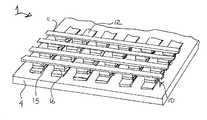
- FIG. 1shows a schematic view of a memory cell 10 that incorporates various aspects of the invention discussed above.
- the memory cell 10includes an upper electrode 11 and a lower electrode 12 with a layer stack interposed therebetween.
- the layer stackforms a memory element 14 having an upper, active layer 15 in contact with upper electrode 11 and a lower, passive layer 16 in contact with lower electrode 12 .
- the passive layer 16is a source (i.e., donor) and acceptor of a charged species, illustratively positively charged ions (typically metal ions) and the active layer 15 is a relatively high resistance material (e.g., an insulator) including a plurality of micro-channels or pores extending generally vertically between the passive layer 16 and the Lipper electrode 11 for facilitating injection and transport of ions in the active layer 15 .
- a sourcei.e., donor
- acceptor of a charged speciestypically metal ions
- the active layer 15is a relatively high resistance material (e.g., an insulator) including a plurality of micro-channels or pores extending generally vertically between the passive layer 16 and the Lipper electrode 11 for facilitating injection and transport of ions in the active layer 15 .
- the first and second electrically conductive electrodes 11 and 12are made of copper, although the electrodes 11 and 12 may be made of any suitable material, such as those listed above.
- the electrodes 11 and 12may be made from about 3,000 to about 8,000 Angstroms thick.
- the active layer 15includes polyphenylacetylene (PPA) but may include any suitable material as discussed above.
- the active layer 15may be made from about 50 to about 1,000 Angstroms thick, with 100 Angstroms presently preferred.
- the passive layer 16includes copper sulfide, but may include other super-ionic materials.
- the passive layer 16may be made from about 20 to about 100 Angstroms thick, with 50 Angstroms presently preferred.
- a barrier layer positioned between the active and passive layersmay be made barrier layer 4 from about 20 to about 300 Angstroms thick, with 50 Angstroms presently preferred.
- the memory cell 10When the memory cell 10 is in a high resistance, low conductivity state, charged species are generally confined to the passive layer 16 and the micro-channels or pores formed by the polymer in the active layer 15 are substantially devoid of charged species.
- the memory cell 10When the memory cell 10 is in a low resistance, high conductivity state, ions from the passive layer 16 are donated into the micro-channels or pores of the active layer 15 to form electrically conductive “nano-wires” or to otherwise dope the active layer 15 , e.g., after application of a suitable electric field.
- Electrodes 11 and 12may be sufficient to both program and read the memory element 14 . That is, an electrical signal applied to the electrodes 11 and 12 may be used to cause charged species movement in the memory cell 10 to program the cell and used to read information stored by the cell, e.g., in the form of a resistance.
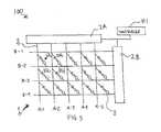
- FIG. 2shows a memory 1 having a plurality of memory cells 10 forned on a substrate 4 .
- the substrate 4may be any suitable material, such as silicon, a polymer film or other.
- the electrodes 12are formed on the substrate 3 as metal strips or lines, but could be formed in other ways, e.g., each electrode formed as an individual pad.
- the passive layer 16 of each cell 10is formed on the electrodes 12 , with the active layer 15 on top of the passive layer 16 and the electrodes 11 formed as metal strips or lines over the active layers 15 .
- the strips that form the electrodes 11are formed at right angles to the strips that form the electrodes 12 , but any suitable angle may be used.
- the memory 1is shown in FIG.
- the memory 1may have a three dimensional (3D) structure with memory cells 10 formed on top of other memory cells 10 .
- 3D arraysmemory cells 10 may be arranged in 2D layers that are stacked one on each other.
- an insulating materialmay be provided as will be understood by those of skill in the art.
- Individual cells 10may be addressed using a matrix addressing scheme, e.g., by applying suitable electrical signals to the strips that form the electrodes 11 and 12 .
- each memory cell 10may be associated with a transistor or other switch to allow individual addressing of memory cells 10 .
- FIG. 3shows a schematic block diagram of a data processing system 100 that includes a memory 1 in accordance with at least one aspect of the invention.
- the system 100includes a controller 101 , which may include any suitable microprocessor or other data processing device, and may program the memory 1 to store information and read stored information from the memory 1 .
- the memory cells 10are addressed by a controller 101 via addressing circuits 2 A and 2 B and addressing lines 3 .
- the addressing circuits 2 A and 2 Bmay allow the controller 101 to send and receive signals to specific memory cells 10 or groups of memory cells 10 .
- a diode as shown in FIG. 3a transistor switch or other device included for each memory cell 10 may allow for individual addressing of the memory cells 10 .
- the memory 1may be controlled to store information, i.e., programmed, based on a signal that applies a reverse bias voltage to a diode associated with the cell.
- the diodemay be configured to normally have a very high resistance to a reverse bias voltage, but exhibit a low resistance to reverse bias voltages that exceed the diode's breakdown voltage.
- the controller 101may apply a reverse bias voltage across the memory cell 10 that exceeds the diode's breakdown voltage to cause an electric field to be created between, or a current to pass between, the first electrode 11 and the second electrode 12 of the memory cell.
- the electric field or currentmay cause the memory cell 10 to change state, and therefore store information.
- memory cells 10may be read using a forward bias voltage applied across the diode.
- a memory cell 10may be programmed in two or more states.
- an electric field and/or current applied to the memory cell 10may cause charged species movement in the memory cell 10 such that the resistance of the active layer 15 is changed.
- the duration that the field is present and/or the current passes through the memory cell 10may determine the information stored by the memory cell 10 .
- current passing through the memory cell 10 for a first amount of timemay cause the memory cell 10 to store a first value
- current passing for a second, longer amount of timemay cause the memory cell 10 to store a second value.
- different voltage levelsmay cause the memory cell 10 to store different information.
- Multi-bit or multi-state programmingin which a memory cell 10 is capable of storing three or more different values may be used.
- a memory cell 10may be programmed between two or more different resistance states where each discrete resistance state represents a different stored value.
- Data retention characteristics of the memory cellmay be controlled based on the mobility of charged particles in the active and/or passive layers.
- controlmay, for example, be achieved by providing appropriately selecting materials for the active and/or passive layers, or in some embodiments, providing at least one barrier layer for impeding motion of the charged particles in the absence of an applied electrical field.
- the arrangement of the active/passive layers and or the barrier layermay limit spontaneous movement of the charged particles (i.e., movement in the absence of an externally applied electric field) between the active layer and the passive layer, thereby increasing the data retention time of the memory device.
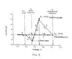
- FIG. 4shows a current (I)-voltage (V) plot for illustrating operation of a memory cell in accordance with the invention.
- Vcurrent-voltage
- charged species from the passive layermay be mobilized by the applied electric field, introduced into the active layer, and arranged into conductive micro-chaninels or other suitable arrangements.
- the decrease in resistance of the memory cellmay correspond to the formation of the electrically conductive nano-wires or other features, thereby storing information in the cell in the form of a resistance.
- Multi-bit programmingmay be achieved by varying the extent to which charged species are introduced into the active layer. For example, stopping programming at different points along the curve 2 may provide the memory cell with different resistance values. If these different resistance values can be distinguished when reading the memory cell, they may be exploited to provide the memory cell with a multi-bit programming capability.
- the memorycan be read at any voltage below the threshold voltage V T , i.e., the “read region”.
- a low voltagemay be used to probe the device and check its resistance.
- a low currentmay indicate the device is in the high resistance, “off” state, and a high current may indicate the device is in a lower resistance, “on” state.
- the “read” operationmay be non-destructive and not disturb the programmed state of the device. From the lowest resistance state at the intersection between curves 2 and 3 , the applied voltage may be reduced towards 0 V along curve 3 .
- the slope of the 1-V curveindicates the memory is in a low resistance state, since the steeper the slope of the I-V curve, the lower the resistance.
- the “on/off ratio”which may be as high as 9 orders of magnitude for the inventive devices, i.e., from several M ohms to ⁇ 100-200 ohms, but typically is ⁇ 4-6 orders of magnitude.
- erasemay be performed by applying an increasingly negative voltage (along curve 3 ) until the erase threshold voltage V E is reached, at which point the device switches back to the high resistance “off” state along curve 4 . Therefore, “erasing” may put the memory cell in a state that represents a stored value, e.g., a logical 0. Alternately, erasing may merely ready the memory cell for programming to store information values.
- Erase threshold voltages V Eare typically in the same range as programming threshold voltages V T , but can be tuned depending upon the choice of materials for the active and passive layers, electrodes, and layer thicknesses. In conceptual terms, an erase operation corresponds to the removal of a minimum amount of charged species sufficient to adjust the resistance of the cell. As a consequence, only a small number of particles may need to be removed from the active layer to effectively change the resistance.
- Switching of the memory between a high resistance “off” state (corresponding to a logical 0) and a lower resistance “on” state (corresponding to a logical 1)may occur quickly, i.e., on the order of about 100 nsec., indicating high operational speed during programming.
- the various layers in a memory cell 10may be formed in any suitable way.
- the passive layer in a memory cellmay be formed by reacting an electrode layer with a suitable material instead of actually placing a material on the electrode layer.
- FIG. 5shows steps in a method for forming one or more memory cells.
- one or more electrodesare formed on a substrate.
- one or more layers of copper or other suitable materialmay be deposited on an insulating substrate by conventional thin film deposition techniques such as thermal evaporation, sputtering, e-beam evaporation, etc.
- the copper or other materialmay be deposited in any suitable arrangement, such as individual pads, strips or other shapes, to any suitable thickness, such as 100 to 400 Angstroms.
- the one or more electrodesare exposed to a material to form a passive layer on the electrode(s).
- the copper electrodesmay be exposed to an admixture gas of nitrogen having 2% hydrogen sulfide (H 2 S) in a chamber at 80 degrees Celsius for approximately 30 minutes. Exposing the copper layer to the H 2 S gas causes a copper sulfide (Cu 2-x S) layer to form on the copper electrode(s).
- Cu 2-x Sis a super-ionic material that readily donates and accepts charged species, and thus forms a passive layer over the copper electrode(s).
- an active layer including an organic polymermay be formed over the passive layer.
- the organic polymermay be deposited using well-known thin film deposition techniques, such as thermal evaporation, spin coating, CVD, etc.
- an organic polymer layermay be self-assembled on the passive layer by exposing the passive layer to a monomer gas. Any suitable polymer, such as those listed above, may be used to form the active layer.
- step S 40one or more electrodes are formed over the active layer(s) to form one or more memory cells.
- the electrodes formed over the active layermay be formed using any suitable process and using any suitable material.
- an organic polymermay be self-assembled to form an active layer in a memory cell.
- FIG. 6shows a set of steps in a method for forming one or more memory cells in a memory.
- step S 110one or more first electrodes are formed on a substrate.
- one or more layers of copper or other suitable materialmay be deposited on an insulating substrate by conventional thin film deposition techniques such as thermal evaporation, sputtering, e-beam evaporation, etc.
- the copper or other materialmay be deposited in any suitable arrangement, such as individual pads, strips or other shapes, to any suitable thickness, such as 100 to 400 Angstroms.
- a passive layeris formed over the first electrode(s).
- the passive layer(s)may be made of any suitable material, such as those listed above, and may be formed in any suitable way.
- the passive layer(s)may be formed by CVD, spin coating, thermal evaporation, etc.
- the passive layer(s)may also be made by exposing the electrode(s) to a material to form a passive layer on the electrode(s).
- copper electrode(s)may be exposed to a hydrogen sulfide (H 2 S) gas in a chamber at room temperature for approximately 10-15 minutes to form a layer of copper sulfide (Cu 2-x S).
- H 2 Shydrogen sulfide
- a polymer layermay be formed over the passive layer by self-assembly.
- the memory cellmay be placed in a chamber in which a monomer gas or liquid is provided.
- the memory cellmay be exposed to the monomer gas or liquid at a suitable temperature (or other suitable temperature) for a suitable period of time.
- passive layermay be exposed to a gas including a monomer of phenylacetylene (or an admixture of monomers of phenylacetylene and diphenylacetylene) at 125 degrees Celsius for approximately 3 hours.
- the monomer componentsmay self-assemble on the passive layer to form a layer of organic polymer.
- the monomer componentsmay join together on the passive layer to form a layer of polymer suitable for the active layer.
- the passive layer(s)may be surrounded by a dielectric, insulating or other suitable material so that the layer of organic polymer self-assembles only on the passive layer and not on portions around the passive layer.
- the passive layermay provide an adhesion layer for the monomer so that the monomer only self-assembles on the passive layer, and not the portions around the passive layer, e.g., dielectric or insulating portions between memory cells.
- step S 140one or more second electrodes are formed over the active layer(s) to form one or more memory cells.
- the electrodes formed over the active layermay be formed using any suitable process and using any suitable material.
- inventive devices or cells fabricated according to the inventive concept and methodologyreflect the extreme flexibility and versatility with regard to device structures and materials selection afforded by the present invention.
- the inventive devicesare well suited for use in a variety of applications currently employing conventional semiconductor-based memory devices.
- the inventive memory devicesare readily fabricated in cost-effective manner utilizing conventional manufacturing technologies.
- the controller 101 in the embodiments abovemay include any suitable general purpose data processing system, which can be, or include a suitably programmed, general purpose computer or network of general purpose computers and other associated devices such as communication devices and/or other circuitry or components necessary to perform the desired input/output or other functions.
- the controller 101can be implemented, at least in part, as single special purpose integrated circuits, e.g., ASICs or an array of ASICs, each having a main or central processor section for overall, system-level control and separate sections dedicated to performing various different specific computations, functions and other processes under the control of the central processor section.
- the controller 101can also be implemented using a plurality of separate dedicated programmable integrated or other electronic circuits or devices, e.g., hard wired electronic or logic circuits, such as discrete element circuits or programmable logic devices.
- the controller 101also can include other devices, such as information display devices (monitors, printers, display lights, etc.), user input devices (a keyboard, user pointing device, touch screen or other user interface), data storage devices, communication devices, airflow sensors, or other electronic circuitry or components.
Landscapes
- Engineering & Computer Science (AREA)
- Chemical & Material Sciences (AREA)
- Nanotechnology (AREA)
- Computer Hardware Design (AREA)
- Physics & Mathematics (AREA)
- Mathematical Physics (AREA)
- Theoretical Computer Science (AREA)
- Crystallography & Structural Chemistry (AREA)
- Semiconductor Memories (AREA)
Abstract
Description
Claims (26)
Priority Applications (1)
| Application Number | Priority Date | Filing Date | Title |
|---|---|---|---|
| US10/413,818US6858481B2 (en) | 2001-08-13 | 2003-04-15 | Memory device with active and passive layers |
Applications Claiming Priority (4)
| Application Number | Priority Date | Filing Date | Title |
|---|---|---|---|
| PCT/RU2001/000334WO2003017282A1 (en) | 2001-08-13 | 2001-08-13 | Memory cell |
| US10/238,880US6815286B2 (en) | 2001-08-13 | 2002-09-11 | Memory device |
| US10/304,863US6806526B2 (en) | 2001-08-13 | 2002-11-27 | Memory device |
| US10/413,818US6858481B2 (en) | 2001-08-13 | 2003-04-15 | Memory device with active and passive layers |
Related Parent Applications (3)
| Application Number | Title | Priority Date | Filing Date |
|---|---|---|---|
| PCT/RU2001/000334Continuation-In-PartWO2003017282A1 (en) | 2001-08-13 | 2001-08-13 | Memory cell |
| US10/238,880Continuation-In-PartUS6815286B2 (en) | 2001-08-13 | 2002-09-11 | Memory device |
| US10/304,863Continuation-In-PartUS6806526B2 (en) | 2001-08-13 | 2002-11-27 | Memory device |
Publications (2)
| Publication Number | Publication Date |
|---|---|
| US20030173612A1 US20030173612A1 (en) | 2003-09-18 |
| US6858481B2true US6858481B2 (en) | 2005-02-22 |
Family
ID=46282238
Family Applications (1)
| Application Number | Title | Priority Date | Filing Date |
|---|---|---|---|
| US10/413,818Expired - Fee RelatedUS6858481B2 (en) | 2001-08-13 | 2003-04-15 | Memory device with active and passive layers |
Country Status (1)
| Country | Link |
|---|---|
| US (1) | US6858481B2 (en) |
Cited By (88)
| Publication number | Priority date | Publication date | Assignee | Title |
|---|---|---|---|---|
| US7102156B1 (en)* | 2004-12-23 | 2006-09-05 | Spansion Llc Advanced Micro Devices, Inc | Memory elements using organic active layer |
| US20060214183A1 (en)* | 2005-03-22 | 2006-09-28 | Spansion Llc | Variable breakdown characteristic diode |
| US20060215439A1 (en)* | 2005-03-22 | 2006-09-28 | Spansion Llc | Temperature compensation of thin film diode voltage threshold in memory sensing circuit |
| US20060245235A1 (en)* | 2005-05-02 | 2006-11-02 | Advanced Micro Devices, Inc. | Design and operation of a resistance switching memory cell with diode |
| US20070020919A1 (en)* | 2005-07-01 | 2007-01-25 | Spansion Llc | Preamorphization to minimize void formation |
| US20070025166A1 (en)* | 2005-07-27 | 2007-02-01 | Spansion Llc | Program/erase waveshaping control to increase data retention of a memory cell |
| US20070090343A1 (en)* | 2005-10-21 | 2007-04-26 | Spansion Llc | System and method for processing an organic memory cell |
| US20070230235A1 (en)* | 2004-11-26 | 2007-10-04 | C/O Semiconductor Energy Laboratory Co., Ltd. | Semiconductor Device |
| US7288782B1 (en) | 2005-01-12 | 2007-10-30 | Spansion Llc | Use of Ta-capped metal line to improve formation of memory element films |
| DE102006038077A1 (en)* | 2006-07-25 | 2008-01-31 | Altis Semiconductor | Solid electrolyte storage cell comprises cathode, anode and solid electrolytes, where anode has intercalation material and metal species, which are unfixed in intercalation material |
| US7344913B1 (en) | 2005-04-06 | 2008-03-18 | Spansion Llc | Spin on memory cell active layer doped with metal ions |
| US20080135834A1 (en)* | 2006-12-08 | 2008-06-12 | Spansion Llc | Prevention of oxidation of carrier ions to improve memory retention properties of polymer memory cell |
| US20080239790A1 (en)* | 2007-03-27 | 2008-10-02 | Herner S Brad | Method to form a memory cell comprising a carbon nanotube fabric element and a steering element |
| US20080237599A1 (en)* | 2007-03-27 | 2008-10-02 | Herner S Brad | Memory cell comprising a carbon nanotube fabric element and a steering element |
| US20090014707A1 (en)* | 2006-10-20 | 2009-01-15 | Wei Lu | Non-volatile solid state resistive switching devices |
| US20090166610A1 (en)* | 2007-12-31 | 2009-07-02 | April Schricker | Memory cell with planarized carbon nanotube layer and methods of forming the same |
| US20090166609A1 (en)* | 2007-12-31 | 2009-07-02 | April Schricker | Memory cell that employs a selectively fabricated carbon nano-tube reversible resistance-switching element formed over a bottom conductor and methods of forming the same |
| WO2009088888A3 (en)* | 2007-12-31 | 2009-09-17 | Sandisk 3D, Llc | Memory cell that employs a selectively fabricated carbon nano-tube reversible resistance-switching element and methods of forming the same |
| US20090256131A1 (en)* | 2008-04-11 | 2009-10-15 | Sandisk 3D Llc | Memory cell that employs a selectively fabricated carbon nano-tube reversible resistance-switching element formed over a bottom conductor and methods of forming the same |
| US20090256130A1 (en)* | 2008-04-11 | 2009-10-15 | Sandisk 3D Llc | Memory cell that employs a selectively fabricated carbon nano-tube reversible resistance-switching element, and methods of forming the same |
| US7776682B1 (en) | 2005-04-20 | 2010-08-17 | Spansion Llc | Ordered porosity to direct memory element formation |
| US20100213433A1 (en)* | 2009-02-20 | 2010-08-26 | Kabushiki Kaisha Toshiba | Non-volatile semiconductor storage device and method of manufacturing the same |
| US20110001117A1 (en)* | 2008-01-21 | 2011-01-06 | President And Fellows Of Harvard College | Nanoscale wire-based memory devices |
| US8012673B1 (en) | 2005-03-01 | 2011-09-06 | Spansion Llc | Processing a copolymer to form a polymer memory cell |
| US20120007037A1 (en)* | 2010-07-09 | 2012-01-12 | Micron Technology, Inc. | CROSS-POINT MEMORY UTILIZING Ru/Si DIODE |
| CN102593359A (en)* | 2012-03-13 | 2012-07-18 | 福州大学 | Multifunction-integrated organic resistive random access memory and manufacturing method thereof |
| US8374018B2 (en) | 2010-07-09 | 2013-02-12 | Crossbar, Inc. | Resistive memory using SiGe material |
| US8391049B2 (en) | 2010-09-29 | 2013-03-05 | Crossbar, Inc. | Resistor structure for a non-volatile memory device and method |
| US8394670B2 (en) | 2011-05-31 | 2013-03-12 | Crossbar, Inc. | Vertical diodes for non-volatile memory device |
| US8399881B2 (en) | 2005-03-25 | 2013-03-19 | Semiconductor Energy Laboratory Co., Ltd. | Memory element, memory device, and semiconductor device |
| US8404553B2 (en) | 2010-08-23 | 2013-03-26 | Crossbar, Inc. | Disturb-resistant non-volatile memory device and method |
| US8441835B2 (en) | 2010-06-11 | 2013-05-14 | Crossbar, Inc. | Interface control for improved switching in RRAM |
| US8450710B2 (en) | 2011-05-27 | 2013-05-28 | Crossbar, Inc. | Low temperature p+ silicon junction material for a non-volatile memory device |
| US8450209B2 (en) | 2010-11-05 | 2013-05-28 | Crossbar, Inc. | p+ Polysilicon material on aluminum for non-volatile memory device and method |
| US8467227B1 (en) | 2010-11-04 | 2013-06-18 | Crossbar, Inc. | Hetero resistive switching material layer in RRAM device and method |
| US8492195B2 (en) | 2010-08-23 | 2013-07-23 | Crossbar, Inc. | Method for forming stackable non-volatile resistive switching memory devices |
| US8519485B2 (en) | 2010-06-11 | 2013-08-27 | Crossbar, Inc. | Pillar structure for memory device and method |
| US8558212B2 (en) | 2010-09-29 | 2013-10-15 | Crossbar, Inc. | Conductive path in switching material in a resistive random access memory device and control |
| US8658476B1 (en) | 2012-04-20 | 2014-02-25 | Crossbar, Inc. | Low temperature P+ polycrystalline silicon material for non-volatile memory device |
| US8659929B2 (en) | 2011-06-30 | 2014-02-25 | Crossbar, Inc. | Amorphous silicon RRAM with non-linear device and operation |
| US8716098B1 (en) | 2012-03-09 | 2014-05-06 | Crossbar, Inc. | Selective removal method and structure of silver in resistive switching device for a non-volatile memory device |
| US8765566B2 (en) | 2012-05-10 | 2014-07-01 | Crossbar, Inc. | Line and space architecture for a non-volatile memory device |
| US8791010B1 (en) | 2010-12-31 | 2014-07-29 | Crossbar, Inc. | Silver interconnects for stacked non-volatile memory device and method |
| US8796658B1 (en) | 2012-05-07 | 2014-08-05 | Crossbar, Inc. | Filamentary based non-volatile resistive memory device and method |
| US8809831B2 (en) | 2010-07-13 | 2014-08-19 | Crossbar, Inc. | On/off ratio for non-volatile memory device and method |
| US8815696B1 (en) | 2010-12-31 | 2014-08-26 | Crossbar, Inc. | Disturb-resistant non-volatile memory device using via-fill and etchback technique |
| US8878235B2 (en) | 2007-12-31 | 2014-11-04 | Sandisk 3D Llc | Memory cell that employs a selectively fabricated carbon nano-tube reversible resistance-switching element and methods of forming the same |
| US8884261B2 (en) | 2010-08-23 | 2014-11-11 | Crossbar, Inc. | Device switching using layered device structure |
| US8889521B1 (en) | 2012-09-14 | 2014-11-18 | Crossbar, Inc. | Method for silver deposition for a non-volatile memory device |
| US8930174B2 (en) | 2010-12-28 | 2015-01-06 | Crossbar, Inc. | Modeling technique for resistive random access memory (RRAM) cells |
| US8934280B1 (en) | 2013-02-06 | 2015-01-13 | Crossbar, Inc. | Capacitive discharge programming for two-terminal memory cells |
| US8947908B2 (en) | 2010-11-04 | 2015-02-03 | Crossbar, Inc. | Hetero-switching layer in a RRAM device and method |
| US8946673B1 (en) | 2012-08-24 | 2015-02-03 | Crossbar, Inc. | Resistive switching device structure with improved data retention for non-volatile memory device and method |
| US8946046B1 (en) | 2012-05-02 | 2015-02-03 | Crossbar, Inc. | Guided path for forming a conductive filament in RRAM |
| US8946669B1 (en) | 2012-04-05 | 2015-02-03 | Crossbar, Inc. | Resistive memory device and fabrication methods |
| US8982647B2 (en) | 2012-11-14 | 2015-03-17 | Crossbar, Inc. | Resistive random access memory equalization and sensing |
| US9012307B2 (en) | 2010-07-13 | 2015-04-21 | Crossbar, Inc. | Two terminal resistive switching device structure and method of fabricating |
| US9087576B1 (en) | 2012-03-29 | 2015-07-21 | Crossbar, Inc. | Low temperature fabrication method for a three-dimensional memory device and structure |
| US9112145B1 (en) | 2013-01-31 | 2015-08-18 | Crossbar, Inc. | Rectified switching of two-terminal memory via real time filament formation |
| US9153623B1 (en) | 2010-12-31 | 2015-10-06 | Crossbar, Inc. | Thin film transistor steering element for a non-volatile memory device |
| US9191000B2 (en) | 2011-07-29 | 2015-11-17 | Crossbar, Inc. | Field programmable gate array utilizing two-terminal non-volatile memory |
| US9252191B2 (en) | 2011-07-22 | 2016-02-02 | Crossbar, Inc. | Seed layer for a p+ silicon germanium material for a non-volatile memory device and method |
| US9312483B2 (en) | 2012-09-24 | 2016-04-12 | Crossbar, Inc. | Electrode structure for a non-volatile memory device and method |
| US9324942B1 (en) | 2013-01-31 | 2016-04-26 | Crossbar, Inc. | Resistive memory cell with solid state diode |
| US9401475B1 (en) | 2010-08-23 | 2016-07-26 | Crossbar, Inc. | Method for silver deposition for a non-volatile memory device |
| US9406379B2 (en) | 2013-01-03 | 2016-08-02 | Crossbar, Inc. | Resistive random access memory with non-linear current-voltage relationship |
| US9412790B1 (en) | 2012-12-04 | 2016-08-09 | Crossbar, Inc. | Scalable RRAM device architecture for a non-volatile memory device and method |
| US9520557B2 (en) | 2008-10-20 | 2016-12-13 | The Regents Of The University Of Michigan | Silicon based nanoscale crossbar memory |
| US9543359B2 (en) | 2011-05-31 | 2017-01-10 | Crossbar, Inc. | Switching device having a non-linear element |
| US9564587B1 (en) | 2011-06-30 | 2017-02-07 | Crossbar, Inc. | Three-dimensional two-terminal memory with enhanced electric field and segmented interconnects |
| US9570678B1 (en) | 2010-06-08 | 2017-02-14 | Crossbar, Inc. | Resistive RAM with preferental filament formation region and methods |
| US9576616B2 (en) | 2012-10-10 | 2017-02-21 | Crossbar, Inc. | Non-volatile memory with overwrite capability and low write amplification |
| US9583701B1 (en) | 2012-08-14 | 2017-02-28 | Crossbar, Inc. | Methods for fabricating resistive memory device switching material using ion implantation |
| USRE46335E1 (en) | 2010-11-04 | 2017-03-07 | Crossbar, Inc. | Switching device having a non-linear element |
| US9601692B1 (en) | 2010-07-13 | 2017-03-21 | Crossbar, Inc. | Hetero-switching layer in a RRAM device and method |
| US9601690B1 (en) | 2011-06-30 | 2017-03-21 | Crossbar, Inc. | Sub-oxide interface layer for two-terminal memory |
| US9620206B2 (en) | 2011-05-31 | 2017-04-11 | Crossbar, Inc. | Memory array architecture with two-terminal memory cells |
| US9627443B2 (en) | 2011-06-30 | 2017-04-18 | Crossbar, Inc. | Three-dimensional oblique two-terminal memory with enhanced electric field |
| US9633723B2 (en) | 2011-06-23 | 2017-04-25 | Crossbar, Inc. | High operating speed resistive random access memory |
| US9685608B2 (en) | 2012-04-13 | 2017-06-20 | Crossbar, Inc. | Reduced diffusion in metal electrode for two-terminal memory |
| US9729155B2 (en) | 2011-07-29 | 2017-08-08 | Crossbar, Inc. | Field programmable gate array utilizing two-terminal non-volatile memory |
| US9735358B2 (en) | 2012-08-14 | 2017-08-15 | Crossbar, Inc. | Noble metal / non-noble metal electrode for RRAM applications |
| US9741765B1 (en) | 2012-08-14 | 2017-08-22 | Crossbar, Inc. | Monolithically integrated resistive memory using integrated-circuit foundry compatible processes |
| US9947719B2 (en) | 2009-11-30 | 2018-04-17 | Micron Technology, Inc. | Memory including a selector switch on a variable resistance memory cell |
| US10056907B1 (en) | 2011-07-29 | 2018-08-21 | Crossbar, Inc. | Field programmable gate array utilizing two-terminal non-volatile memory |
| US10290801B2 (en) | 2014-02-07 | 2019-05-14 | Crossbar, Inc. | Scalable silicon based resistive memory device |
| DE102007019260B4 (en) | 2007-04-17 | 2020-01-16 | Novaled Gmbh | Non-volatile organic storage element |
| US11068620B2 (en) | 2012-11-09 | 2021-07-20 | Crossbar, Inc. | Secure circuit integrated with memory layer |
Families Citing this family (63)
| Publication number | Priority date | Publication date | Assignee | Title |
|---|---|---|---|---|
| WO2003017282A1 (en)* | 2001-08-13 | 2003-02-27 | Advanced Micro Devices, Inc. | Memory cell |
| WO2004070789A2 (en)* | 2003-02-03 | 2004-08-19 | The Regent Of The University Of California | Rewritable nano-surface organic electrical bistable devices |
| US6921912B2 (en)* | 2003-06-03 | 2005-07-26 | Micron Technology, Inc. | Diode/superionic conductor/polymer memory structure |
| US6787458B1 (en)* | 2003-07-07 | 2004-09-07 | Advanced Micro Devices, Inc. | Polymer memory device formed in via opening |
| US7274035B2 (en)* | 2003-09-03 | 2007-09-25 | The Regents Of The University Of California | Memory devices based on electric field programmable films |
| DE10345403A1 (en)* | 2003-09-30 | 2005-04-28 | Infineon Technologies Ag | Material and cell construction for storage applications |
| US6852586B1 (en)* | 2003-10-01 | 2005-02-08 | Advanced Micro Devices, Inc. | Self assembly of conducting polymer for formation of polymer memory cell |
| US7015504B2 (en)* | 2003-11-03 | 2006-03-21 | Advanced Micro Devices, Inc. | Sidewall formation for high density polymer memory element array |
| WO2005086627A2 (en)* | 2003-12-03 | 2005-09-22 | The Regents Of The University Of California | Three-terminal electrical bistable devices |
| US6956761B2 (en)* | 2004-03-10 | 2005-10-18 | Micron Technology, Inc. | Method to manufacture polymer memory with copper ion switching species |
| US8383226B2 (en)* | 2004-03-12 | 2013-02-26 | University Of Maryland | Structures and methods for increasing the speed of electroactive polymers |
| US20050212022A1 (en)* | 2004-03-24 | 2005-09-29 | Greer Edward C | Memory cell having an electric field programmable storage element, and method of operating same |
| US7608855B2 (en)* | 2004-04-02 | 2009-10-27 | Spansion Llc | Polymer dielectrics for memory element array interconnect |
| WO2006001923A2 (en) | 2004-05-17 | 2006-01-05 | The Regents Of The University Of California | Bistable nanoparticle- polymer composite for use in memory devices |
| US7554111B2 (en)* | 2004-05-20 | 2009-06-30 | The Regents Of The University Of California | Nanoparticle-polymer bistable devices |
| US7157732B2 (en)* | 2004-07-01 | 2007-01-02 | Spansion Llc | Switchable memory diode-a new memory device |
| KR100609699B1 (en)* | 2004-07-15 | 2006-08-08 | 한국전자통신연구원 | 2-terminal semiconductor device using abrupt metal-insulator transition semiconductor material and manufacturing method thereof |
| US7199394B2 (en)* | 2004-08-17 | 2007-04-03 | Spansion Llc | Polymer memory device with variable period of retention time |
| US7289353B2 (en)* | 2004-08-17 | 2007-10-30 | Spansion, Llc | Systems and methods for adjusting programming thresholds of polymer memory cells |
| GB2437188A (en)* | 2004-10-28 | 2007-10-17 | Univ California | Organic-complex thin film for nonvolatile memory applications |
| US7220642B2 (en)* | 2004-11-12 | 2007-05-22 | Spansion Llc | Protection of active layers of memory cells during processing of other elements |
| EP1820215A4 (en)* | 2004-12-07 | 2008-11-12 | Semiconductor Energy Lab | MEMORY DEVICE AND SEMICONDUCTOR DEVICE |
| US7379317B2 (en)* | 2004-12-23 | 2008-05-27 | Spansion Llc | Method of programming, reading and erasing memory-diode in a memory-diode array |
| US7105374B1 (en)* | 2005-01-12 | 2006-09-12 | Spansion Llc | Memory cell containing copolymer containing diarylacetylene portion |
| US7344912B1 (en)* | 2005-03-01 | 2008-03-18 | Spansion Llc | Method for patterning electrically conducting poly(phenyl acetylene) and poly(diphenyl acetylene) |
| US8098521B2 (en)* | 2005-03-31 | 2012-01-17 | Spansion Llc | Method of providing an erase activation energy of a memory device |
| US20070007585A1 (en)* | 2005-07-05 | 2007-01-11 | Spansion Llc | Memory device with improved data retention |
| US20070009821A1 (en)* | 2005-07-08 | 2007-01-11 | Charlotte Cutler | Devices containing multi-bit data |
| US7525194B2 (en)* | 2005-07-27 | 2009-04-28 | Palo Alto Research Center Incorporated | System including self-assembled interconnections |
| US7662708B2 (en)* | 2005-07-27 | 2010-02-16 | Palo Alto Research Center Incorporated | Self-assembled interconnection particles |
| US7633129B1 (en)* | 2005-09-16 | 2009-12-15 | Spansion Llc | Memory devices with active and passive layers having multiple self-assembled sublayers |
| EP1997226A1 (en)* | 2006-03-10 | 2008-12-03 | Nxp B.V. | Pulse shaping circuit for crystal oscillator |
| EP1850378A3 (en)* | 2006-04-28 | 2013-08-07 | Semiconductor Energy Laboratory Co., Ltd. | Memory device and semicondutor device |
| US7499304B2 (en)* | 2006-07-31 | 2009-03-03 | Sandisk 3D Llc | Systems for high bandwidth one time field-programmable memory |
| US7499355B2 (en)* | 2006-07-31 | 2009-03-03 | Sandisk 3D Llc | High bandwidth one time field-programmable memory |
| WO2008016833A2 (en)* | 2006-07-31 | 2008-02-07 | Sandisk 3D Llc | Increasing write voltage pulse operations in non-volatile memory |
| US7492630B2 (en)* | 2006-07-31 | 2009-02-17 | Sandisk 3D Llc | Systems for reverse bias trim operations in non-volatile memory |
| US7522448B2 (en)* | 2006-07-31 | 2009-04-21 | Sandisk 3D Llc | Controlled pulse operations in non-volatile memory |
| US7719874B2 (en)* | 2006-07-31 | 2010-05-18 | Sandisk 3D Llc | Systems for controlled pulse operations in non-volatile memory |
| US7495947B2 (en)* | 2006-07-31 | 2009-02-24 | Sandisk 3D Llc | Reverse bias trim operations in non-volatile memory |
| US8766224B2 (en) | 2006-10-03 | 2014-07-01 | Hewlett-Packard Development Company, L.P. | Electrically actuated switch |
| FR2915616B1 (en)* | 2007-04-27 | 2010-08-20 | Centre Nat Rech Scient | DEVICE AND METHOD FOR STORING INFORMATION MASS. |
| US7978507B2 (en)* | 2008-06-27 | 2011-07-12 | Sandisk 3D, Llc | Pulse reset for non-volatile storage |
| EP2361438B1 (en) | 2008-10-29 | 2013-05-15 | Hewlett-Packard Development Company, L.P. | Electrically actuated device and method of controlling the formation of dopants therein |
| US8264864B2 (en)* | 2008-12-19 | 2012-09-11 | Unity Semiconductor Corporation | Memory device with band gap control |
| WO2010074685A1 (en)* | 2008-12-23 | 2010-07-01 | Hewlett-Packard Development Company, L.P. | Memristive device having a porous dopant diffusion element |
| US8891283B2 (en)* | 2009-01-05 | 2014-11-18 | Hewlett-Packard Development Company, L.P. | Memristive device based on current modulation by trapped charges |
| US8431921B2 (en)* | 2009-01-13 | 2013-04-30 | Hewlett-Packard Development Company, L.P. | Memristor having a triangular shaped electrode |
| WO2010085225A1 (en) | 2009-01-26 | 2010-07-29 | Hewlett-Packard Development Company, L.P. | Controlled placement of dopants in memristor active regions |
| US8450711B2 (en) | 2009-01-26 | 2013-05-28 | Hewlett-Packard Development Company, L.P. | Semiconductor memristor devices |
| WO2010087835A1 (en)* | 2009-01-29 | 2010-08-05 | Hewlett-Packard Development Company, L.P. | Electrically actuated devices |
| US8750024B2 (en)* | 2009-06-18 | 2014-06-10 | Hewlett-Packard Development Company, L.P. | Memcapacitor |
| CN102648528B (en)* | 2009-06-25 | 2016-02-17 | 惠普开发有限公司 | Switchable Junctions with Intrinsic Diodes with Different Switching Thresholds |
| KR101530118B1 (en)* | 2009-07-10 | 2015-06-18 | 휴렛-팩커드 디벨롭먼트 컴퍼니, 엘.피. | Memristive junction with intrinsic rectifier |
| US8575585B2 (en) | 2009-07-13 | 2013-11-05 | Hewlett-Packard Development Company, L.P. | Memristive device |
| WO2011028208A1 (en) | 2009-09-04 | 2011-03-10 | Hewlett-Packard Development Company, L.P. | Memristors based on mixed-metal-valence compounds |
| US20130234103A1 (en)* | 2009-08-31 | 2013-09-12 | Hewlett-Packard Development Company, L.P. | Nanoscale switching device with an amorphous switching material |
| US8294132B2 (en)* | 2010-03-30 | 2012-10-23 | Hewlett-Packard Development Company, L.P. | Graphene memristor having modulated graphene interlayer conduction |
| US8546785B2 (en) | 2010-03-31 | 2013-10-01 | Hewlett-Packard Development Company, L.P. | Memristive device |
| US9018083B2 (en) | 2011-05-04 | 2015-04-28 | Hewlett-Packard Development Company, L.P. | Electrically actuated device and method of controlling the formation of dopants therein |
| WO2016163978A1 (en)* | 2015-04-06 | 2016-10-13 | Hewlett Packard Enterprise Development Lp | Electrically conducting oxygen diffusion barriers for memristors and selectors |
| DE102015121344B4 (en)* | 2015-12-08 | 2023-11-02 | Infineon Technologies Austria Ag | SEMICONDUCTOR DEVICE AND METHOD FOR PRODUCING SAME |
| US9997475B2 (en) | 2016-01-13 | 2018-06-12 | International Business Machines Corporation | Monolithic integration of III-V cells for powering memory erasure devices |
Citations (96)
| Publication number | Priority date | Publication date | Assignee | Title |
|---|---|---|---|---|
| US3719933A (en) | 1970-04-02 | 1973-03-06 | Matsushita Electric Industrial Co Ltd | Memory device having lead dioxide particles therein |
| US3810127A (en) | 1970-06-23 | 1974-05-07 | Intel Corp | Programmable circuit {13 {11 the method of programming thereof and the devices so programmed |
| US4267558A (en) | 1979-01-05 | 1981-05-12 | Texas Instruments Incorporated | Electrically erasable memory with self-limiting erase |
| US4267583A (en) | 1978-11-27 | 1981-05-12 | Nippon Electric Co., Ltd. | Memory test device with write and pseudo write signals |
| US4371883A (en) | 1980-03-14 | 1983-02-01 | The Johns Hopkins University | Current controlled bistable electrical organic thin film switching device |
| US4616340A (en) | 1981-10-14 | 1986-10-07 | Agency Of Industrial Science & Technology | Non-volatile semiconductor memory |
| US4631562A (en) | 1985-05-31 | 1986-12-23 | Rca Corporation | Zener diode structure |
| US4652894A (en) | 1980-03-14 | 1987-03-24 | The Johns Hopkins University | Electrical organic thin film switching device switching between detectably different oxidation states |
| US4677742A (en) | 1983-01-18 | 1987-07-07 | Energy Conversion Devices, Inc. | Electronic matrix arrays and method for making the same |
| US4727514A (en) | 1986-02-11 | 1988-02-23 | Texas Instruments Incorporated | Programmable memory with memory cells programmed by addressing |
| US4733375A (en) | 1984-05-28 | 1988-03-22 | Seiko Epson Corporation | Non-volatile memory circuit |
| EP0268370A2 (en) | 1986-10-13 | 1988-05-25 | Canon Kabushiki Kaisha | Switching device |
| US4834911A (en) | 1986-08-25 | 1989-05-30 | Electro-Organic Company | Intrinsically conductive and semiconductive polymers, products formed with such polymers and methods of forming same |
| US4839700A (en) | 1987-12-16 | 1989-06-13 | California Institute Of Technology | Solid-state non-volatile electronically programmable reversible variable resistance device |
| US4860254A (en) | 1986-01-31 | 1989-08-22 | Bayer Aktiengesellschaft | Non-volatile electronic memory |
| EP0385688A2 (en) | 1989-02-27 | 1990-09-05 | Matsushita Electric Industrial Co., Ltd. | Ferroelectric liquid crystal composition and ferroelectric liquid crystal display device |
| US5012445A (en) | 1987-10-13 | 1991-04-30 | Hitachi, Ltd. | Programmable read only memory being capable of controlling internal writing voltage of external voltage |
| US5034192A (en) | 1984-11-23 | 1991-07-23 | Massachusetts Institute Of Technology | Molecule-based microelectronic devices |
| US5130380A (en) | 1990-05-29 | 1992-07-14 | Carew Evan B | Conductive polymers |
| US5136212A (en) | 1988-02-18 | 1992-08-04 | Canon Kabushiki Kaisha | Electron emitting device, electron generator employing said electron emitting device, and method for driving said generator |
| US5153681A (en) | 1989-07-25 | 1992-10-06 | Matsushita Electric Industrial Co., Ltd. | Electrcally plastic device and its control method |
| WO1993004506A1 (en) | 1991-08-19 | 1993-03-04 | Energy Conversion Devices, Inc. | Electrically erasable, directly overwritable, multibit single cell memory elements and arrays fabricated therefrom |
| US5196912A (en) | 1988-10-28 | 1993-03-23 | Casio Computer Co., Ltd. | Thin film transistor having memory function and method for using thin film transistor as memory element |
| US5206525A (en) | 1989-12-27 | 1993-04-27 | Nippon Petrochemicals Co., Ltd. | Electric element capable of controlling the electric conductivity of π-conjugated macromolecular materials |
| US5245543A (en) | 1990-12-21 | 1993-09-14 | Texas Instruments Incorporated | Method and apparatus for integrated circuit design |
| US5296716A (en) | 1991-01-18 | 1994-03-22 | Energy Conversion Devices, Inc. | Electrically erasable, directly overwritable, multibit single cell memory elements and arrays fabricated therefrom |
| US5315131A (en) | 1990-11-22 | 1994-05-24 | Matsushita Electric Industrial Co., Ltd. | Electrically reprogrammable nonvolatile memory device |
| US5355235A (en) | 1991-08-15 | 1994-10-11 | Kabushiki Kaisha Toshiba | Organic field effect element having organic layers with different carrier concentrations |
| US5392236A (en) | 1992-06-30 | 1995-02-21 | Nec Corporation | Semiconductor memory device |
| JPH07106440A (en) | 1993-10-04 | 1995-04-21 | Hitachi Ltd | Nonvolatile semiconductor memory device and application system using the same |
| US5412614A (en) | 1991-08-16 | 1995-05-02 | U.S. Philips Corporation | Electronic matrix array devices and systems incorporating such devices |
| US5431883A (en) | 1991-01-24 | 1995-07-11 | Commissariat Energie Atomique | Detector for the detection of chemical species or photons using a field effect transistor |
| US5440518A (en) | 1991-06-12 | 1995-08-08 | Hazani; Emanuel | Non-volatile memory circuits, architecture and methods |
| EP0727822A2 (en) | 1995-02-14 | 1996-08-21 | Canon Kabushiki Kaisha | Semiconductor memory device |
| US5563081A (en) | 1992-03-23 | 1996-10-08 | Rohm Co., Inc. | Method for making a nonvolatile memory device utilizing a field effect transistor having a ferroelectric gate film |
| US5572472A (en) | 1995-04-14 | 1996-11-05 | Delco Electronics Corporation | Integrated zener-zap nonvolatile memory cell with programming and pretest capability |
| US5579199A (en) | 1992-11-26 | 1996-11-26 | Sharp Kabushiki Kaisha | Non-volatile memory device and a method for producing the same |
| RU2071126C1 (en) | 1992-08-27 | 1996-12-27 | Кригер Юрий Генрихович | Storage element |
| US5670818A (en) | 1990-04-12 | 1997-09-23 | Actel Corporation | Electrically programmable antifuse |
| US5691935A (en) | 1995-07-13 | 1997-11-25 | Douglass; Barry G. | Memory element and method of operation thereof |
| US5698874A (en) | 1993-11-02 | 1997-12-16 | Sony Corporation | Photoelectric cell having first and second insulated gates on first and second channel forming regions |
| US5734605A (en) | 1996-09-10 | 1998-03-31 | Motorola, Inc. | Multi-layer magnetic tunneling junction memory cells |
| DE19640239A1 (en) | 1996-09-30 | 1998-04-02 | Siemens Ag | Storage cell with polymer capacitor |
| US5761115A (en) | 1996-05-30 | 1998-06-02 | Axon Technologies Corporation | Programmable metallization cell structure and method of making same |
| US5770885A (en) | 1990-04-12 | 1998-06-23 | Actel Corporation | Electrically programmable antifuse incorporating dielectric and amorphous silicon interlayers |
| US5818749A (en) | 1993-08-20 | 1998-10-06 | Micron Technology, Inc. | Integrated circuit memory device |
| US5849403A (en) | 1995-09-13 | 1998-12-15 | Kabushiki Kaisha Toshiba | Organic thin film device |
| WO1999004440A1 (en) | 1997-07-14 | 1999-01-28 | Technion Research And Development Foundation Ltd. | Microelectronic components and electronic networks comprising dna |
| US5869882A (en) | 1994-09-30 | 1999-02-09 | Texas Instruments Incorporated | Zener diode structure with high reverse breakdown voltage |
| WO1999008325A2 (en) | 1997-07-22 | 1999-02-18 | Thin Film Electronics Asa | Electrode means, with or without functional elements and an electrode device formed of said means |
| WO1999014762A1 (en) | 1997-09-01 | 1999-03-25 | Thin Film Electronics Asa | A read-only memory and read-only memory device |
| WO1999019900A2 (en) | 1997-10-14 | 1999-04-22 | Patterning Technologies Limited | Method of forming an electronic device |
| US5900662A (en) | 1995-11-06 | 1999-05-04 | Sgs Thomson Microelectronics S.R.L. | MOS technology power device with low output resistance and low capacitance, and related manufacturing process |
| US6055180A (en) | 1997-06-17 | 2000-04-25 | Thin Film Electronics Asa | Electrically addressable passive device, method for electrical addressing of the same and uses of the device and the method |
| US6060338A (en) | 1989-01-10 | 2000-05-09 | Mitsubishi Denki Kabushiki Kaisha | Method of making a field effect transistor |
| WO2000026918A1 (en) | 1998-10-30 | 2000-05-11 | Nikolai Schwabe | Magnetic storage device |
| US6064589A (en) | 1998-02-02 | 2000-05-16 | Walker; Darryl G. | Double gate DRAM memory cell |
| US6088319A (en) | 1995-06-23 | 2000-07-11 | Thin Film Electronics Asa | Method for writing of data in an optical memory, apparatus for performing the method and optical memory formed thereby |
| WO2000048196A1 (en) | 1999-02-11 | 2000-08-17 | Arizona Board Of Regents | Programmable microelectronic devices and methods of forming and programming same |
| US6118684A (en) | 1997-10-03 | 2000-09-12 | Yihong; Wu | Optical memories using electron trapping material |
| US6128214A (en) | 1999-03-29 | 2000-10-03 | Hewlett-Packard | Molecular wire crossbar memory |
| US6150705A (en) | 1993-07-07 | 2000-11-21 | Actel Corporation | Dielectric-polysilicon-dielectric-polysilicon-dielectric antifuse for field programmable logic application |
| DE19959904A1 (en) | 1999-12-11 | 2001-06-28 | Edward William Schlag | Regulating electric current through medium, useful as molecular switch in electronics or chemical process control, involves changing parameter inhibiting internal motion of adjacent molecular sections of chain molecule |
| US20010014038A1 (en) | 1998-02-19 | 2001-08-16 | Sanyo Electric Co., Ltd. | Write circuit for a semiconductor memory device |
| US6288697B1 (en) | 1996-11-15 | 2001-09-11 | Sharp Kabushiki Kaisha | Method and circuit for driving display device |
| US6292396B1 (en) | 1999-04-21 | 2001-09-18 | Stmicroelectronics S.A. | Method and device for the programming of an electrically programmable non-volatile memory for improved reliability |
| US20010055384A1 (en) | 2000-03-22 | 2001-12-27 | Shunpei Yamazaki | Electronic device |
| US20010054709A1 (en) | 1999-03-29 | 2001-12-27 | Heath James R. | Chemically synthesized and assembled electronic devices |
| US6349054B1 (en) | 2000-12-25 | 2002-02-19 | Mitsubishi Denki Kabushiki Kaisha | Thin film magnetic memory device including memory cells having a magnetic tunnel junction |
| US20020027819A1 (en) | 1999-02-12 | 2002-03-07 | David Tomanek | Nanocapsules containing charged particles, their uses and methods of forming same |
| WO2002035580A2 (en) | 2000-10-24 | 2002-05-02 | Molecular Electronics Corporation | Three-terminal field-controlled molecular devices |
| US6384427B1 (en) | 1999-10-29 | 2002-05-07 | Semiconductor Energy Laboratory Co., Ltd. | Electronic device |
| WO2002037500A1 (en) | 2000-10-31 | 2002-05-10 | The Regents Of The University Of California | Organic bistable device and organic memory cells |
| WO2002043071A1 (en) | 2000-11-27 | 2002-05-30 | Thin Film Electronics Asa | A ferroelectric memory circuit and method for its fabrication |
| US6403396B1 (en) | 1998-01-28 | 2002-06-11 | Thin Film Electronics Asa | Method for generation of electrically conducting or semiconducting structures in three dimensions and methods for erasure of the same structures |
| US6403397B1 (en) | 2000-06-28 | 2002-06-11 | Agere Systems Guardian Corp. | Process for fabricating organic semiconductor device involving selective patterning |
| US6407953B1 (en) | 2001-02-02 | 2002-06-18 | Matrix Semiconductor, Inc. | Memory array organization and related test method particularly well suited for integrated circuits having write-once memory arrays |
| US6418049B1 (en) | 1997-12-04 | 2002-07-09 | Arizona Board Of Regents | Programmable sub-surface aggregating metallization structure and method of making same |
| US6424553B2 (en) | 2000-03-22 | 2002-07-23 | Thin Film Electronics Asa | Multidimensional addressing architecture for electronic devices |
| US6426891B1 (en) | 1999-10-27 | 2002-07-30 | Sony Corporation | Nonvolatile memory with a two-terminal switching element and its driving method |
| US20020101763A1 (en) | 2001-02-01 | 2002-08-01 | Mitsubishi Denki Kabushiki Kaisha | Non-volatile semiconductor memory device |
| US6429457B1 (en) | 1998-01-16 | 2002-08-06 | Thin Film Electronics Asa | Field-effect transistor |
| US20020104889A1 (en) | 2000-09-25 | 2002-08-08 | Forrest Stephen R. | Smart card composed of organic processing elements |
| US6449184B2 (en) | 2000-06-19 | 2002-09-10 | Matsushita Electric Industrial Co., Ltd. | Method for driving semiconductor memory |
| US20020125504A1 (en) | 2001-03-07 | 2002-09-12 | Perlov Craig M. | Fabrication and assembly structures and methods for memory devices |
| WO2002078003A2 (en) | 2001-03-21 | 2002-10-03 | Matrix Semiconductor, Inc. | Method and apparatus for biasing selected and unselected array lines when writing a memory array |
| US6461916B1 (en) | 1997-03-28 | 2002-10-08 | Hitachi, Ltd. | Non-volatile semiconductor memory and method of making same, and semiconductor device and method of making the device |
| US20020163030A1 (en) | 2001-05-07 | 2002-11-07 | Coatue Corporation | Floating gate memory device using composite molecular material |
| US20020163831A1 (en) | 2001-05-07 | 2002-11-07 | Coatue Corporation | Molecular memory cell |
| US20020163829A1 (en) | 2001-05-07 | 2002-11-07 | Coatue Corporation | Memory switch |
| US20020163828A1 (en) | 2001-05-07 | 2002-11-07 | Coatue Corporation | Memory device with a self-assembled polymer film and method of making the same |
| US20020163057A1 (en) | 2001-05-07 | 2002-11-07 | Coatue Corporation | Reversible field-programmable electric interconnects |
| US20020163830A1 (en) | 2001-05-07 | 2002-11-07 | Coatue Corporation | Molecular memory device |
| US20020168820A1 (en) | 2000-09-08 | 2002-11-14 | Kozicki Michael N. | Microelectronic programmable device and methods of forming and programming the same |
| US6487106B1 (en) | 1999-01-12 | 2002-11-26 | Arizona Board Of Regents | Programmable microelectronic devices and method of forming and programming same |
| WO2003017282A1 (en) | 2001-08-13 | 2003-02-27 | Advanced Micro Devices, Inc. | Memory cell |
- 2003
- 2003-04-15USUS10/413,818patent/US6858481B2/ennot_activeExpired - Fee Related
Patent Citations (112)
| Publication number | Priority date | Publication date | Assignee | Title |
|---|---|---|---|---|
| US3719933A (en) | 1970-04-02 | 1973-03-06 | Matsushita Electric Industrial Co Ltd | Memory device having lead dioxide particles therein |
| US3810127A (en) | 1970-06-23 | 1974-05-07 | Intel Corp | Programmable circuit {13 {11 the method of programming thereof and the devices so programmed |
| US4267583A (en) | 1978-11-27 | 1981-05-12 | Nippon Electric Co., Ltd. | Memory test device with write and pseudo write signals |
| US4267558A (en) | 1979-01-05 | 1981-05-12 | Texas Instruments Incorporated | Electrically erasable memory with self-limiting erase |
| US4652894A (en) | 1980-03-14 | 1987-03-24 | The Johns Hopkins University | Electrical organic thin film switching device switching between detectably different oxidation states |
| US4371883A (en) | 1980-03-14 | 1983-02-01 | The Johns Hopkins University | Current controlled bistable electrical organic thin film switching device |
| US4616340A (en) | 1981-10-14 | 1986-10-07 | Agency Of Industrial Science & Technology | Non-volatile semiconductor memory |
| US4677742A (en) | 1983-01-18 | 1987-07-07 | Energy Conversion Devices, Inc. | Electronic matrix arrays and method for making the same |
| US4733375A (en) | 1984-05-28 | 1988-03-22 | Seiko Epson Corporation | Non-volatile memory circuit |
| USRE34974E (en) | 1984-05-28 | 1995-06-20 | Seiko Epson Corporation | Non-volatile memory circuit |
| US5034192A (en) | 1984-11-23 | 1991-07-23 | Massachusetts Institute Of Technology | Molecule-based microelectronic devices |
| US4631562A (en) | 1985-05-31 | 1986-12-23 | Rca Corporation | Zener diode structure |
| US4860254A (en) | 1986-01-31 | 1989-08-22 | Bayer Aktiengesellschaft | Non-volatile electronic memory |
| US4727514A (en) | 1986-02-11 | 1988-02-23 | Texas Instruments Incorporated | Programmable memory with memory cells programmed by addressing |
| US4834911A (en) | 1986-08-25 | 1989-05-30 | Electro-Organic Company | Intrinsically conductive and semiconductive polymers, products formed with such polymers and methods of forming same |
| EP0268370A2 (en) | 1986-10-13 | 1988-05-25 | Canon Kabushiki Kaisha | Switching device |
| EP0268370A3 (en) | 1986-10-13 | 1989-05-31 | Canon Kabushiki Kaisha | Switching device |
| US5012445A (en) | 1987-10-13 | 1991-04-30 | Hitachi, Ltd. | Programmable read only memory being capable of controlling internal writing voltage of external voltage |
| US4839700A (en) | 1987-12-16 | 1989-06-13 | California Institute Of Technology | Solid-state non-volatile electronically programmable reversible variable resistance device |
| US5136212A (en) | 1988-02-18 | 1992-08-04 | Canon Kabushiki Kaisha | Electron emitting device, electron generator employing said electron emitting device, and method for driving said generator |
| US5196912A (en) | 1988-10-28 | 1993-03-23 | Casio Computer Co., Ltd. | Thin film transistor having memory function and method for using thin film transistor as memory element |
| US6060338A (en) | 1989-01-10 | 2000-05-09 | Mitsubishi Denki Kabushiki Kaisha | Method of making a field effect transistor |
| EP0385688A2 (en) | 1989-02-27 | 1990-09-05 | Matsushita Electric Industrial Co., Ltd. | Ferroelectric liquid crystal composition and ferroelectric liquid crystal display device |
| US5153681A (en) | 1989-07-25 | 1992-10-06 | Matsushita Electric Industrial Co., Ltd. | Electrcally plastic device and its control method |
| US5206525A (en) | 1989-12-27 | 1993-04-27 | Nippon Petrochemicals Co., Ltd. | Electric element capable of controlling the electric conductivity of π-conjugated macromolecular materials |
| US5770885A (en) | 1990-04-12 | 1998-06-23 | Actel Corporation | Electrically programmable antifuse incorporating dielectric and amorphous silicon interlayers |
| US5670818A (en) | 1990-04-12 | 1997-09-23 | Actel Corporation | Electrically programmable antifuse |
| US5130380A (en) | 1990-05-29 | 1992-07-14 | Carew Evan B | Conductive polymers |
| US5315131A (en) | 1990-11-22 | 1994-05-24 | Matsushita Electric Industrial Co., Ltd. | Electrically reprogrammable nonvolatile memory device |
| US5245543A (en) | 1990-12-21 | 1993-09-14 | Texas Instruments Incorporated | Method and apparatus for integrated circuit design |
| US5319564A (en) | 1990-12-21 | 1994-06-07 | Texas Instruments Incorporated | Method and apparatus for integrated circuit design |
| US5296716A (en) | 1991-01-18 | 1994-03-22 | Energy Conversion Devices, Inc. | Electrically erasable, directly overwritable, multibit single cell memory elements and arrays fabricated therefrom |
| US5431883A (en) | 1991-01-24 | 1995-07-11 | Commissariat Energie Atomique | Detector for the detection of chemical species or photons using a field effect transistor |
| US5440518A (en) | 1991-06-12 | 1995-08-08 | Hazani; Emanuel | Non-volatile memory circuits, architecture and methods |
| US5355235A (en) | 1991-08-15 | 1994-10-11 | Kabushiki Kaisha Toshiba | Organic field effect element having organic layers with different carrier concentrations |
| US5412614A (en) | 1991-08-16 | 1995-05-02 | U.S. Philips Corporation | Electronic matrix array devices and systems incorporating such devices |
| WO1993004506A1 (en) | 1991-08-19 | 1993-03-04 | Energy Conversion Devices, Inc. | Electrically erasable, directly overwritable, multibit single cell memory elements and arrays fabricated therefrom |
| US5563081A (en) | 1992-03-23 | 1996-10-08 | Rohm Co., Inc. | Method for making a nonvolatile memory device utilizing a field effect transistor having a ferroelectric gate film |
| US5392236A (en) | 1992-06-30 | 1995-02-21 | Nec Corporation | Semiconductor memory device |
| RU2071126C1 (en) | 1992-08-27 | 1996-12-27 | Кригер Юрий Генрихович | Storage element |
| US5579199A (en) | 1992-11-26 | 1996-11-26 | Sharp Kabushiki Kaisha | Non-volatile memory device and a method for producing the same |
| US6150705A (en) | 1993-07-07 | 2000-11-21 | Actel Corporation | Dielectric-polysilicon-dielectric-polysilicon-dielectric antifuse for field programmable logic application |
| US5818749A (en) | 1993-08-20 | 1998-10-06 | Micron Technology, Inc. | Integrated circuit memory device |
| JPH07106440A (en) | 1993-10-04 | 1995-04-21 | Hitachi Ltd | Nonvolatile semiconductor memory device and application system using the same |
| US5698874A (en) | 1993-11-02 | 1997-12-16 | Sony Corporation | Photoelectric cell having first and second insulated gates on first and second channel forming regions |
| US5869882A (en) | 1994-09-30 | 1999-02-09 | Texas Instruments Incorporated | Zener diode structure with high reverse breakdown voltage |
| EP0727822A2 (en) | 1995-02-14 | 1996-08-21 | Canon Kabushiki Kaisha | Semiconductor memory device |
| US5572472A (en) | 1995-04-14 | 1996-11-05 | Delco Electronics Corporation | Integrated zener-zap nonvolatile memory cell with programming and pretest capability |
| US6088319A (en) | 1995-06-23 | 2000-07-11 | Thin Film Electronics Asa | Method for writing of data in an optical memory, apparatus for performing the method and optical memory formed thereby |
| US5691935A (en) | 1995-07-13 | 1997-11-25 | Douglass; Barry G. | Memory element and method of operation thereof |
| US5849403A (en) | 1995-09-13 | 1998-12-15 | Kabushiki Kaisha Toshiba | Organic thin film device |
| US5900662A (en) | 1995-11-06 | 1999-05-04 | Sgs Thomson Microelectronics S.R.L. | MOS technology power device with low output resistance and low capacitance, and related manufacturing process |
| US5914893A (en) | 1996-05-30 | 1999-06-22 | Axon Technologies Corporation | Programmable metallization cell structure and method of making same |
| US5896312A (en) | 1996-05-30 | 1999-04-20 | Axon Technologies Corporation | Programmable metallization cell structure and method of making same |
| US5761115A (en) | 1996-05-30 | 1998-06-02 | Axon Technologies Corporation | Programmable metallization cell structure and method of making same |
| US5734605A (en) | 1996-09-10 | 1998-03-31 | Motorola, Inc. | Multi-layer magnetic tunneling junction memory cells |
| DE19640239A1 (en) | 1996-09-30 | 1998-04-02 | Siemens Ag | Storage cell with polymer capacitor |
| US6288697B1 (en) | 1996-11-15 | 2001-09-11 | Sharp Kabushiki Kaisha | Method and circuit for driving display device |
| US6461916B1 (en) | 1997-03-28 | 2002-10-08 | Hitachi, Ltd. | Non-volatile semiconductor memory and method of making same, and semiconductor device and method of making the device |
| US6055180A (en) | 1997-06-17 | 2000-04-25 | Thin Film Electronics Asa | Electrically addressable passive device, method for electrical addressing of the same and uses of the device and the method |
| WO1999004440A1 (en) | 1997-07-14 | 1999-01-28 | Technion Research And Development Foundation Ltd. | Microelectronic components and electronic networks comprising dna |
| US6326936B1 (en) | 1997-07-22 | 2001-12-04 | Thin Film Electronics Asa | Electrode means, comprising polymer materials, with or without functional elements and an electrode device formed of said means |
| WO1999008325A2 (en) | 1997-07-22 | 1999-02-18 | Thin Film Electronics Asa | Electrode means, with or without functional elements and an electrode device formed of said means |
| WO1999014762A1 (en) | 1997-09-01 | 1999-03-25 | Thin Film Electronics Asa | A read-only memory and read-only memory device |
| US6118684A (en) | 1997-10-03 | 2000-09-12 | Yihong; Wu | Optical memories using electron trapping material |
| WO1999019900A2 (en) | 1997-10-14 | 1999-04-22 | Patterning Technologies Limited | Method of forming an electronic device |
| US6418049B1 (en) | 1997-12-04 | 2002-07-09 | Arizona Board Of Regents | Programmable sub-surface aggregating metallization structure and method of making same |
| US6429457B1 (en) | 1998-01-16 | 2002-08-06 | Thin Film Electronics Asa | Field-effect transistor |
| US6403396B1 (en) | 1998-01-28 | 2002-06-11 | Thin Film Electronics Asa | Method for generation of electrically conducting or semiconducting structures in three dimensions and methods for erasure of the same structures |
| US6432739B1 (en) | 1998-01-28 | 2002-08-13 | Thin Film Electronics Asa | Method for generating electrical conducting or semiconducting structures in two or three dimensions, a method for erasing the same structures and an electric field generator/modulator for use with the method for generating |
| US6064589A (en) | 1998-02-02 | 2000-05-16 | Walker; Darryl G. | Double gate DRAM memory cell |
| US20010014038A1 (en) | 1998-02-19 | 2001-08-16 | Sanyo Electric Co., Ltd. | Write circuit for a semiconductor memory device |
| US6353559B2 (en) | 1998-02-19 | 2002-03-05 | Sanyo Electric Co., Ltd. | Write circuit for a semiconductor memory device |
| WO2000026918A1 (en) | 1998-10-30 | 2000-05-11 | Nikolai Schwabe | Magnetic storage device |
| US6487106B1 (en) | 1999-01-12 | 2002-11-26 | Arizona Board Of Regents | Programmable microelectronic devices and method of forming and programming same |
| WO2000048196A1 (en) | 1999-02-11 | 2000-08-17 | Arizona Board Of Regents | Programmable microelectronic devices and methods of forming and programming same |
| US20020027819A1 (en) | 1999-02-12 | 2002-03-07 | David Tomanek | Nanocapsules containing charged particles, their uses and methods of forming same |
| US6459095B1 (en) | 1999-03-29 | 2002-10-01 | Hewlett-Packard Company | Chemically synthesized and assembled electronics devices |
| US20010054709A1 (en) | 1999-03-29 | 2001-12-27 | Heath James R. | Chemically synthesized and assembled electronic devices |
| US6128214A (en) | 1999-03-29 | 2000-10-03 | Hewlett-Packard | Molecular wire crossbar memory |
| US6292396B1 (en) | 1999-04-21 | 2001-09-18 | Stmicroelectronics S.A. | Method and device for the programming of an electrically programmable non-volatile memory for improved reliability |
| US6426891B1 (en) | 1999-10-27 | 2002-07-30 | Sony Corporation | Nonvolatile memory with a two-terminal switching element and its driving method |
| US6384427B1 (en) | 1999-10-29 | 2002-05-07 | Semiconductor Energy Laboratory Co., Ltd. | Electronic device |
| US20020134979A1 (en) | 1999-10-29 | 2002-09-26 | Semiconductor Energy Laboratory Co., Ltd. | Electronic device |
| DE19959904A1 (en) | 1999-12-11 | 2001-06-28 | Edward William Schlag | Regulating electric current through medium, useful as molecular switch in electronics or chemical process control, involves changing parameter inhibiting internal motion of adjacent molecular sections of chain molecule |
| US20010055384A1 (en) | 2000-03-22 | 2001-12-27 | Shunpei Yamazaki | Electronic device |
| US6424553B2 (en) | 2000-03-22 | 2002-07-23 | Thin Film Electronics Asa | Multidimensional addressing architecture for electronic devices |
| US6449184B2 (en) | 2000-06-19 | 2002-09-10 | Matsushita Electric Industrial Co., Ltd. | Method for driving semiconductor memory |
| US6403397B1 (en) | 2000-06-28 | 2002-06-11 | Agere Systems Guardian Corp. | Process for fabricating organic semiconductor device involving selective patterning |
| US20020168820A1 (en) | 2000-09-08 | 2002-11-14 | Kozicki Michael N. | Microelectronic programmable device and methods of forming and programming the same |
| US20020104889A1 (en) | 2000-09-25 | 2002-08-08 | Forrest Stephen R. | Smart card composed of organic processing elements |
| WO2002035580A2 (en) | 2000-10-24 | 2002-05-02 | Molecular Electronics Corporation | Three-terminal field-controlled molecular devices |
| WO2002037500A1 (en) | 2000-10-31 | 2002-05-10 | The Regents Of The University Of California | Organic bistable device and organic memory cells |
| WO2002043071A1 (en) | 2000-11-27 | 2002-05-30 | Thin Film Electronics Asa | A ferroelectric memory circuit and method for its fabrication |
| US6349054B1 (en) | 2000-12-25 | 2002-02-19 | Mitsubishi Denki Kabushiki Kaisha | Thin film magnetic memory device including memory cells having a magnetic tunnel junction |
| US20020101763A1 (en) | 2001-02-01 | 2002-08-01 | Mitsubishi Denki Kabushiki Kaisha | Non-volatile semiconductor memory device |
| US6407953B1 (en) | 2001-02-02 | 2002-06-18 | Matrix Semiconductor, Inc. | Memory array organization and related test method particularly well suited for integrated circuits having write-once memory arrays |
| US20020125504A1 (en) | 2001-03-07 | 2002-09-12 | Perlov Craig M. | Fabrication and assembly structures and methods for memory devices |
| WO2002078003A2 (en) | 2001-03-21 | 2002-10-03 | Matrix Semiconductor, Inc. | Method and apparatus for biasing selected and unselected array lines when writing a memory array |
| US20020163030A1 (en) | 2001-05-07 | 2002-11-07 | Coatue Corporation | Floating gate memory device using composite molecular material |
| US20020163828A1 (en) | 2001-05-07 | 2002-11-07 | Coatue Corporation | Memory device with a self-assembled polymer film and method of making the same |
| US20020163057A1 (en) | 2001-05-07 | 2002-11-07 | Coatue Corporation | Reversible field-programmable electric interconnects |
| US20020163830A1 (en) | 2001-05-07 | 2002-11-07 | Coatue Corporation | Molecular memory device |
| WO2002091384A1 (en) | 2001-05-07 | 2002-11-14 | Advanced Micro Devices, Inc. | A memory device with a self-assembled polymer film and method of making the same |
| WO2002091385A1 (en) | 2001-05-07 | 2002-11-14 | Advanced Micro Devices, Inc. | Molecular memory cell |
| WO2002091494A1 (en) | 2001-05-07 | 2002-11-14 | Advanced Micro Devices, Inc. | Switch element having memeory effect |
| WO2002091496A2 (en) | 2001-05-07 | 2002-11-14 | Advanced Micro Devices, Inc. | Reversible field-programmable electric interconnects |
| WO2002091476A1 (en) | 2001-05-07 | 2002-11-14 | Advanced Micro Devices, Inc. | Floating gate memory device using composite molecular material |
| WO2002091495A2 (en) | 2001-05-07 | 2002-11-14 | Coatue Corporation | Molecular memory device |
| US20020163831A1 (en) | 2001-05-07 | 2002-11-07 | Coatue Corporation | Molecular memory cell |
| US20020163829A1 (en) | 2001-05-07 | 2002-11-07 | Coatue Corporation | Memory switch |
| WO2003017282A1 (en) | 2001-08-13 | 2003-02-27 | Advanced Micro Devices, Inc. | Memory cell |
Non-Patent Citations (38)
| Title |
|---|
| "A Disrupted Organic Film: Could Memories Be Made of This?," ORNL Review, vol. 33, No. 2, 2000. |
| "Technical Summary of Programmable Metallization Cell Memory Technology," Version 1.3, Dec. 2001. |
| "The 1998 Conference Archive," The Sixth Foresight Conference on Molecular Nanotechnology, Nov. 12-15, 1998, www.foresight.org/Conferences/MNT6/index.html. |
| Beck, A. et al., "Reproducible Switching Effect in Thin Oxide Films for Memory Applications," Applied Physics Letters, vol. 77, No. 1, pp. 139-141, Jul. 3, 2000. |
| Bernard, Allen, "A Big Name in Chips Helps Coatue in Molecular Memory Race," Aug. 27, 2000, www.nanoelectronicsplanet.com/features/article/0,4028,6571-1452831,00.html. |
| Chen, J. et al., "Room-temperature Negative Differential Resistance in Nanoscale Molecular Junctions," Applied Physics Letters, vol. 77, No. 8, Aug. 21, 2000. |
| Collier, C. P. et al., "Electrically Configurable Molecular-Based Logic Gates," Science, vol. 285, pp. 391-394, Jul 16, 1999. |
| Gannon, Andrew, "Toward the Next Generation CD," Physical Review Focus, Feb. 16, 2000. |
| Gao, H. et al., "Using a New Kind of Organic Complex System of Electrical Bistability for Ultrahigh Density Data Storage," J. Vac. Sci. Technol. B vol. 15, No. 4, pp. 1581-1583, Jul./Aug. 1997. |
| Gao, H. J. et al., "Reversible, Nanometer-Scale Conductance Transitions in an Organic Complex," Physical Review Letters, vol. 84, No. 8, pp. 1780-1783, Feb. 21, 2000. |
| International Search Report, PCT/RU01/00334, search completed Feb. 14, 2002. |
| International Search Report, PCT/US02/14236, search completed Aug. 14, 2002. |
| International Search Report, PCT/US02/14237, search completed Sep. 9, 2002. |
| International Search Report, PCT/US02/14238, search completed Aug. 9, 2002. |
| International Search Report, PCT/US02/14239, search completed Aug. 20, 2002. |
| International Search Report, PCT/US02/14269, search completed Mar. 27, 2003. |
| International Search Report, PCT/US02/14270, search completed Mar. 28, 2003. |
| Japanese patent abstract of publication No. 01-103137, Apr. 20, 1989. |
| Japanese patent abstract of publication No. 01278781, Nov. 9, 1989. |
| Japanese patent abstract of publication No. 61107723, May 26, 1986. |
| Japanese patent abstract of publication No. 63293729, Nov. 30, 1998. |
| Krieger, Ju. Hu. et al., "Molecular Analogue Memory Cell Based on Electrical Switching and Memory in Molecular Thin Films," Synthetic Metals, 7730 (2000), pp. 1-4. |
| Krieger, Juri H. et al., "Molecular Analogue Memory Cell," Sixth Foresight Conference on Molecular Nanotechnology, Santa Clara, California, Nov. 12-15, 1998. |
| Krieger, Yu. G. et al., "Study of Test Structures of a Molecular Memory Element," Institute of Inorganic Chemistry, Siberian Branch, Russian Academy of Sciences. Translated from Zhumal Strukturnoi Khimii, vol. 34, No. 6, pp. 152-156, Nov.-Dec. 1993. Original article submitted Apr. 27, 1993. |
| Krieger, Yu. G., "Molecular Electronics: Current State and Future Trends," Journal of Structural Chemistry, vol. 34, No. 6, pp. 896-904, Nov.-Dec. 1993. |
| Krieger, Yu. H., "Structural Instability of One-Dimensional Systems as a Physical Principle Underlying the Functioning of Molecular Electronic Devices," Journal of Structural Chemistry, vol. 40, No. 4, pp. 594-619, Jul.-Aug. 1999. |
| Kurita, Ryo et al., "Field Modulation Effects on Charge-Density-Wave Conduction in NbSe3," Physica B, 284-288 (2000), pp. 1161-1662. |
| Ma, L. P. et al., "Data Storage With 0.7 nm Recording Marks on a Crystalline Organic Thin Film by a Scanning Tunneling Microscope," Applied Physics Letters, vol. 73, No. 6, pp. 850-852, Aug. 10, 1998. |
| Ma, L.P. et al., "Nanometer-Scale Recording on an Organic Complex Thin Film With a Scanning Tunneling Microscope," Applied Physics Letters, vol. 69, No. 24, pp. 3752-3753, Dec. 9, 1996. |
| Machida, Yasuhiko et al., "Electrical Switching in Evaporated Lead Phthalocyanine Films," Japanese Journal of Applied Physics, vol. 28, No. 2, pp. 297-298, Feb. 1989. |
| Ovshinsky, Stanford R., "Localized States in the Gap of Amorphous Semiconductors," Physical Review Letters, vol. 36, No. 24, pp. 1469-1472, Jun. 14, 1976. |
| Potember, R. S. et al., "Electrical Switching and Memory Phenomena in Cu-TCNQ Thin Films," Applied Physics Letters, vol. 34, No. 6, pp. 405-407, Mar. 15, 1979. |
| Reed, M.A. et al., "Molecular Random Access Memory Cell," Applied Physics Letters, vol. 78, No. 23, pp. 3735-3737, Jun. 4, 2001. |
| Rossel, C. et al., "Electrical Current Distribution Across a Metal-Insulator-Metal Structure During Bistable Switching." Apr. 24, 2001. |
| Rotman, David, "Molecular Memory," Technology Review, May 2001. |
| Semiconductor Times, pp. 5-6, Jul. 2002. |
| Stikeman, Alexandra, "Polymer Memory: The Plastic Path to Better Data Storage," Technology Review, p. 31, Sep. 2002. |
| Zhou, C. et al., "Nanoscale Metal/Self-Assembled Monolayer/Metal Heterostructures," Applied Physics Letters, vol. 71, No. 5, pp. 611-613, Aug. 4, 1997. |
Cited By (144)
| Publication number | Priority date | Publication date | Assignee | Title |
|---|---|---|---|---|
| US20100055896A1 (en)* | 2004-11-26 | 2010-03-04 | Semiconductor Energy Laboratory Co., Ltd. | Semiconductor device |
| US8295104B2 (en) | 2004-11-26 | 2012-10-23 | Semiconductor Energy Laboratory Co., Ltd. | Semiconductor device |
| US7688624B2 (en) | 2004-11-26 | 2010-03-30 | Semiconductor Energy Laboratory Co., Ltd. | Semiconductor device |
| US20070230235A1 (en)* | 2004-11-26 | 2007-10-04 | C/O Semiconductor Energy Laboratory Co., Ltd. | Semiconductor Device |
| US7102156B1 (en)* | 2004-12-23 | 2006-09-05 | Spansion Llc Advanced Micro Devices, Inc | Memory elements using organic active layer |
| US7288782B1 (en) | 2005-01-12 | 2007-10-30 | Spansion Llc | Use of Ta-capped metal line to improve formation of memory element films |
| US8012673B1 (en) | 2005-03-01 | 2011-09-06 | Spansion Llc | Processing a copolymer to form a polymer memory cell |
| US7145824B2 (en) | 2005-03-22 | 2006-12-05 | Spansion Llc | Temperature compensation of thin film diode voltage threshold in memory sensing circuit |
| US20060215439A1 (en)* | 2005-03-22 | 2006-09-28 | Spansion Llc | Temperature compensation of thin film diode voltage threshold in memory sensing circuit |
| US7579631B2 (en) | 2005-03-22 | 2009-08-25 | Spansion Llc | Variable breakdown characteristic diode |
| US20060214183A1 (en)* | 2005-03-22 | 2006-09-28 | Spansion Llc | Variable breakdown characteristic diode |
| US8399881B2 (en) | 2005-03-25 | 2013-03-19 | Semiconductor Energy Laboratory Co., Ltd. | Memory element, memory device, and semiconductor device |
| US7344913B1 (en) | 2005-04-06 | 2008-03-18 | Spansion Llc | Spin on memory cell active layer doped with metal ions |
| US7776682B1 (en) | 2005-04-20 | 2010-08-17 | Spansion Llc | Ordered porosity to direct memory element formation |
| US20060245235A1 (en)* | 2005-05-02 | 2006-11-02 | Advanced Micro Devices, Inc. | Design and operation of a resistance switching memory cell with diode |
| US20070020919A1 (en)* | 2005-07-01 | 2007-01-25 | Spansion Llc | Preamorphization to minimize void formation |
| US7361586B2 (en) | 2005-07-01 | 2008-04-22 | Spansion Llc | Preamorphization to minimize void formation |
| US20070025166A1 (en)* | 2005-07-27 | 2007-02-01 | Spansion Llc | Program/erase waveshaping control to increase data retention of a memory cell |
| US20070090343A1 (en)* | 2005-10-21 | 2007-04-26 | Spansion Llc | System and method for processing an organic memory cell |
| US7632706B2 (en) | 2005-10-21 | 2009-12-15 | Spansion Llc | System and method for processing an organic memory cell |
| US8115282B2 (en) | 2006-07-25 | 2012-02-14 | Adesto Technology Corporation | Memory cell device and method of manufacture |
| US20080023798A1 (en)* | 2006-07-25 | 2008-01-31 | Sandra Mege | Memory cells with an anode comprising intercalating material and metal species dispersed therein |
| DE102006038077A1 (en)* | 2006-07-25 | 2008-01-31 | Altis Semiconductor | Solid electrolyte storage cell comprises cathode, anode and solid electrolytes, where anode has intercalation material and metal species, which are unfixed in intercalation material |
| US10134985B2 (en) | 2006-10-20 | 2018-11-20 | The Regents Of The University Of Michigan | Non-volatile solid state resistive switching devices |
| US20090014707A1 (en)* | 2006-10-20 | 2009-01-15 | Wei Lu | Non-volatile solid state resistive switching devices |
| US10090463B2 (en) | 2006-10-20 | 2018-10-02 | The Regents Of The University Of Michigan | Non-volatile solid state resistive switching devices |
| US20080135834A1 (en)* | 2006-12-08 | 2008-06-12 | Spansion Llc | Prevention of oxidation of carrier ions to improve memory retention properties of polymer memory cell |
| US7902086B2 (en) | 2006-12-08 | 2011-03-08 | Spansion Llc | Prevention of oxidation of carrier ions to improve memory retention properties of polymer memory cell |
| US7924602B2 (en) | 2007-03-27 | 2011-04-12 | Sandisk 3D Llc | Method to program a memory cell comprising a carbon nanotube fabric element and a steering element |
| US8203864B2 (en) | 2007-03-27 | 2012-06-19 | Sandisk 3D Llc | Memory cell and methods of forming a memory cell comprising a carbon nanotube fabric element and a steering element |
| US20100142255A1 (en)* | 2007-03-27 | 2010-06-10 | Herner S Brad | Method to program a memory cell comprising a carbon nanotube fabric element and a steering element |
| US20080239790A1 (en)* | 2007-03-27 | 2008-10-02 | Herner S Brad | Method to form a memory cell comprising a carbon nanotube fabric element and a steering element |
| US8847200B2 (en) | 2007-03-27 | 2014-09-30 | Sandisk 3D Llc | Memory cell comprising a carbon nanotube fabric element and a steering element |
| US20080237599A1 (en)* | 2007-03-27 | 2008-10-02 | Herner S Brad | Memory cell comprising a carbon nanotube fabric element and a steering element |
| US7667999B2 (en) | 2007-03-27 | 2010-02-23 | Sandisk 3D Llc | Method to program a memory cell comprising a carbon nanotube fabric and a steering element |
| US7982209B2 (en) | 2007-03-27 | 2011-07-19 | Sandisk 3D Llc | Memory cell comprising a carbon nanotube fabric element and a steering element |
| DE102007019260B4 (en) | 2007-04-17 | 2020-01-16 | Novaled Gmbh | Non-volatile organic storage element |
| US20090166609A1 (en)* | 2007-12-31 | 2009-07-02 | April Schricker | Memory cell that employs a selectively fabricated carbon nano-tube reversible resistance-switching element formed over a bottom conductor and methods of forming the same |
| US8878235B2 (en) | 2007-12-31 | 2014-11-04 | Sandisk 3D Llc | Memory cell that employs a selectively fabricated carbon nano-tube reversible resistance-switching element and methods of forming the same |
| WO2009088888A3 (en)* | 2007-12-31 | 2009-09-17 | Sandisk 3D, Llc | Memory cell that employs a selectively fabricated carbon nano-tube reversible resistance-switching element and methods of forming the same |
| WO2009088890A3 (en)* | 2007-12-31 | 2009-09-17 | Sandisk 3D, Llc | Memory cell with planarized carbon nanotube layer and methods of forming the same |
| US8236623B2 (en) | 2007-12-31 | 2012-08-07 | Sandisk 3D Llc | Memory cell that employs a selectively fabricated carbon nano-tube reversible resistance-switching element and methods of forming the same |
| WO2009088889A1 (en)* | 2007-12-31 | 2009-07-16 | Sandisk 3D, Llc | Memory cell that employs a selectively fabricated carbon nano-tube reversible resistance-switching element formed over a bottom conductor and methods of forming the same |
| US20090166610A1 (en)* | 2007-12-31 | 2009-07-02 | April Schricker | Memory cell with planarized carbon nanotube layer and methods of forming the same |
| US8558220B2 (en) | 2007-12-31 | 2013-10-15 | Sandisk 3D Llc | Memory cell that employs a selectively fabricated carbon nano-tube reversible resistance-switching element formed over a bottom conductor and methods of forming the same |
| US20110001117A1 (en)* | 2008-01-21 | 2011-01-06 | President And Fellows Of Harvard College | Nanoscale wire-based memory devices |
| US20090256130A1 (en)* | 2008-04-11 | 2009-10-15 | Sandisk 3D Llc | Memory cell that employs a selectively fabricated carbon nano-tube reversible resistance-switching element, and methods of forming the same |
| US20090256131A1 (en)* | 2008-04-11 | 2009-10-15 | Sandisk 3D Llc | Memory cell that employs a selectively fabricated carbon nano-tube reversible resistance-switching element formed over a bottom conductor and methods of forming the same |
| US8530318B2 (en) | 2008-04-11 | 2013-09-10 | Sandisk 3D Llc | Memory cell that employs a selectively fabricated carbon nano-tube reversible resistance-switching element formed over a bottom conductor and methods of forming the same |
| US8304284B2 (en) | 2008-04-11 | 2012-11-06 | Sandisk 3D Llc | Memory cell that employs a selectively fabricated carbon nano-tube reversible resistance-switching element, and methods of forming the same |
| US9520557B2 (en) | 2008-10-20 | 2016-12-13 | The Regents Of The University Of Michigan | Silicon based nanoscale crossbar memory |
| US20100213433A1 (en)* | 2009-02-20 | 2010-08-26 | Kabushiki Kaisha Toshiba | Non-volatile semiconductor storage device and method of manufacturing the same |
| US8723157B2 (en) | 2009-02-20 | 2014-05-13 | Kabushiki Kaisha Toshiba | Non-volatile semiconductor storage device and method of manufacturing the same |
| US9947719B2 (en) | 2009-11-30 | 2018-04-17 | Micron Technology, Inc. | Memory including a selector switch on a variable resistance memory cell |
| US10896930B2 (en) | 2009-11-30 | 2021-01-19 | Micron Technology, Inc. | Memory including a selector switch on a variable resistance memory cell |
| US11404479B2 (en) | 2009-11-30 | 2022-08-02 | Micron Technology, Inc. | Memory including a selector switch on a variable resistance memory cell |
| US10374007B2 (en) | 2009-11-30 | 2019-08-06 | Micron Technology, Inc. | Memory including a selector switch on a variable resistance memory cell |
| US9570678B1 (en) | 2010-06-08 | 2017-02-14 | Crossbar, Inc. | Resistive RAM with preferental filament formation region and methods |
| US8441835B2 (en) | 2010-06-11 | 2013-05-14 | Crossbar, Inc. | Interface control for improved switching in RRAM |
| US8519485B2 (en) | 2010-06-11 | 2013-08-27 | Crossbar, Inc. | Pillar structure for memory device and method |
| US8599601B2 (en) | 2010-06-11 | 2013-12-03 | Crossbar, Inc. | Interface control for improved switching in RRAM |
| US8993397B2 (en) | 2010-06-11 | 2015-03-31 | Crossbar, Inc. | Pillar structure for memory device and method |
| US9036400B2 (en) | 2010-07-09 | 2015-05-19 | Crossbar, Inc. | Method and structure of monolithically integrated IC and resistive memory using IC foundry-compatible processes |
| TWI497490B (en)* | 2010-07-09 | 2015-08-21 | Micron Technology Inc | Cross-point memory utilizing ru/si diode |
| US9343674B2 (en) | 2010-07-09 | 2016-05-17 | Micron Technology, Inc. | Cross-point memory utilizing Ru/Si diode |
| US8395140B2 (en)* | 2010-07-09 | 2013-03-12 | Micron Technology, Inc. | Cross-point memory utilizing Ru/Si diode |
| US20120007037A1 (en)* | 2010-07-09 | 2012-01-12 | Micron Technology, Inc. | CROSS-POINT MEMORY UTILIZING Ru/Si DIODE |
| US8374018B2 (en) | 2010-07-09 | 2013-02-12 | Crossbar, Inc. | Resistive memory using SiGe material |
| US8750019B2 (en) | 2010-07-09 | 2014-06-10 | Crossbar, Inc. | Resistive memory using SiGe material |
| US8803125B2 (en) | 2010-07-09 | 2014-08-12 | Micron Technology, Inc. | Cross-point memory utilizing Ru/Si diode |
| US8809831B2 (en) | 2010-07-13 | 2014-08-19 | Crossbar, Inc. | On/off ratio for non-volatile memory device and method |
| US9755143B2 (en) | 2010-07-13 | 2017-09-05 | Crossbar, Inc. | On/off ratio for nonvolatile memory device and method |
| US9012307B2 (en) | 2010-07-13 | 2015-04-21 | Crossbar, Inc. | Two terminal resistive switching device structure and method of fabricating |
| US9601692B1 (en) | 2010-07-13 | 2017-03-21 | Crossbar, Inc. | Hetero-switching layer in a RRAM device and method |
| US9590013B2 (en) | 2010-08-23 | 2017-03-07 | Crossbar, Inc. | Device switching using layered device structure |
| US10224370B2 (en) | 2010-08-23 | 2019-03-05 | Crossbar, Inc. | Device switching using layered device structure |
| US8884261B2 (en) | 2010-08-23 | 2014-11-11 | Crossbar, Inc. | Device switching using layered device structure |
| US9401475B1 (en) | 2010-08-23 | 2016-07-26 | Crossbar, Inc. | Method for silver deposition for a non-volatile memory device |
| US8404553B2 (en) | 2010-08-23 | 2013-03-26 | Crossbar, Inc. | Disturb-resistant non-volatile memory device and method |
| US9035276B2 (en) | 2010-08-23 | 2015-05-19 | Crossbar, Inc. | Stackable non-volatile resistive switching memory device |
| US8648327B2 (en) | 2010-08-23 | 2014-02-11 | Crossbar, Inc. | Stackable non-volatile resistive switching memory devices |
| US8492195B2 (en) | 2010-08-23 | 2013-07-23 | Crossbar, Inc. | Method for forming stackable non-volatile resistive switching memory devices |
| US9412789B1 (en) | 2010-08-23 | 2016-08-09 | Crossbar, Inc. | Stackable non-volatile resistive switching memory device and method of fabricating the same |
| US8558212B2 (en) | 2010-09-29 | 2013-10-15 | Crossbar, Inc. | Conductive path in switching material in a resistive random access memory device and control |
| US8912523B2 (en) | 2010-09-29 | 2014-12-16 | Crossbar, Inc. | Conductive path in switching material in a resistive random access memory device and control |
| US9129887B2 (en) | 2010-09-29 | 2015-09-08 | Crossbar, Inc. | Resistor structure for a non-volatile memory device and method |
| US8391049B2 (en) | 2010-09-29 | 2013-03-05 | Crossbar, Inc. | Resistor structure for a non-volatile memory device and method |
| US8467227B1 (en) | 2010-11-04 | 2013-06-18 | Crossbar, Inc. | Hetero resistive switching material layer in RRAM device and method |
| US8659933B2 (en) | 2010-11-04 | 2014-02-25 | Crossbar, Inc. | Hereto resistive switching material layer in RRAM device and method |
| US8947908B2 (en) | 2010-11-04 | 2015-02-03 | Crossbar, Inc. | Hetero-switching layer in a RRAM device and method |
| USRE46335E1 (en) | 2010-11-04 | 2017-03-07 | Crossbar, Inc. | Switching device having a non-linear element |
| US8450209B2 (en) | 2010-11-05 | 2013-05-28 | Crossbar, Inc. | p+ Polysilicon material on aluminum for non-volatile memory device and method |
| US8930174B2 (en) | 2010-12-28 | 2015-01-06 | Crossbar, Inc. | Modeling technique for resistive random access memory (RRAM) cells |
| US8791010B1 (en) | 2010-12-31 | 2014-07-29 | Crossbar, Inc. | Silver interconnects for stacked non-volatile memory device and method |
| US8815696B1 (en) | 2010-12-31 | 2014-08-26 | Crossbar, Inc. | Disturb-resistant non-volatile memory device using via-fill and etchback technique |
| US9153623B1 (en) | 2010-12-31 | 2015-10-06 | Crossbar, Inc. | Thin film transistor steering element for a non-volatile memory device |
| US9831289B2 (en) | 2010-12-31 | 2017-11-28 | Crossbar, Inc. | Disturb-resistant non-volatile memory device using via-fill and etchback technique |
| US8450710B2 (en) | 2011-05-27 | 2013-05-28 | Crossbar, Inc. | Low temperature p+ silicon junction material for a non-volatile memory device |
| US9543359B2 (en) | 2011-05-31 | 2017-01-10 | Crossbar, Inc. | Switching device having a non-linear element |
| US9620206B2 (en) | 2011-05-31 | 2017-04-11 | Crossbar, Inc. | Memory array architecture with two-terminal memory cells |
| US8394670B2 (en) | 2011-05-31 | 2013-03-12 | Crossbar, Inc. | Vertical diodes for non-volatile memory device |
| US9633723B2 (en) | 2011-06-23 | 2017-04-25 | Crossbar, Inc. | High operating speed resistive random access memory |
| US9601690B1 (en) | 2011-06-30 | 2017-03-21 | Crossbar, Inc. | Sub-oxide interface layer for two-terminal memory |
| US9564587B1 (en) | 2011-06-30 | 2017-02-07 | Crossbar, Inc. | Three-dimensional two-terminal memory with enhanced electric field and segmented interconnects |
| US9570683B1 (en) | 2011-06-30 | 2017-02-14 | Crossbar, Inc. | Three-dimensional two-terminal memory with enhanced electric field and segmented interconnects |
| US9627443B2 (en) | 2011-06-30 | 2017-04-18 | Crossbar, Inc. | Three-dimensional oblique two-terminal memory with enhanced electric field |
| US8659929B2 (en) | 2011-06-30 | 2014-02-25 | Crossbar, Inc. | Amorphous silicon RRAM with non-linear device and operation |
| US9252191B2 (en) | 2011-07-22 | 2016-02-02 | Crossbar, Inc. | Seed layer for a p+ silicon germanium material for a non-volatile memory device and method |
| US9191000B2 (en) | 2011-07-29 | 2015-11-17 | Crossbar, Inc. | Field programmable gate array utilizing two-terminal non-volatile memory |
| US10056907B1 (en) | 2011-07-29 | 2018-08-21 | Crossbar, Inc. | Field programmable gate array utilizing two-terminal non-volatile memory |
| US9729155B2 (en) | 2011-07-29 | 2017-08-08 | Crossbar, Inc. | Field programmable gate array utilizing two-terminal non-volatile memory |
| US8716098B1 (en) | 2012-03-09 | 2014-05-06 | Crossbar, Inc. | Selective removal method and structure of silver in resistive switching device for a non-volatile memory device |
| CN102593359B (en)* | 2012-03-13 | 2014-05-07 | 福州大学 | Multifunction-integrated organic resistive random access memory and manufacturing method thereof |
| CN102593359A (en)* | 2012-03-13 | 2012-07-18 | 福州大学 | Multifunction-integrated organic resistive random access memory and manufacturing method thereof |
| US9087576B1 (en) | 2012-03-29 | 2015-07-21 | Crossbar, Inc. | Low temperature fabrication method for a three-dimensional memory device and structure |
| US8946669B1 (en) | 2012-04-05 | 2015-02-03 | Crossbar, Inc. | Resistive memory device and fabrication methods |
| US9673255B2 (en) | 2012-04-05 | 2017-06-06 | Crossbar, Inc. | Resistive memory device and fabrication methods |
| US9685608B2 (en) | 2012-04-13 | 2017-06-20 | Crossbar, Inc. | Reduced diffusion in metal electrode for two-terminal memory |
| US10910561B1 (en) | 2012-04-13 | 2021-02-02 | Crossbar, Inc. | Reduced diffusion in metal electrode for two-terminal memory |
| US9793474B2 (en) | 2012-04-20 | 2017-10-17 | Crossbar, Inc. | Low temperature P+ polycrystalline silicon material for non-volatile memory device |
| US8658476B1 (en) | 2012-04-20 | 2014-02-25 | Crossbar, Inc. | Low temperature P+ polycrystalline silicon material for non-volatile memory device |
| US9972778B2 (en) | 2012-05-02 | 2018-05-15 | Crossbar, Inc. | Guided path for forming a conductive filament in RRAM |
| US8946046B1 (en) | 2012-05-02 | 2015-02-03 | Crossbar, Inc. | Guided path for forming a conductive filament in RRAM |
| US9385319B1 (en) | 2012-05-07 | 2016-07-05 | Crossbar, Inc. | Filamentary based non-volatile resistive memory device and method |
| US8796658B1 (en) | 2012-05-07 | 2014-08-05 | Crossbar, Inc. | Filamentary based non-volatile resistive memory device and method |
| US8765566B2 (en) | 2012-05-10 | 2014-07-01 | Crossbar, Inc. | Line and space architecture for a non-volatile memory device |
| US9741765B1 (en) | 2012-08-14 | 2017-08-22 | Crossbar, Inc. | Monolithically integrated resistive memory using integrated-circuit foundry compatible processes |
| US9583701B1 (en) | 2012-08-14 | 2017-02-28 | Crossbar, Inc. | Methods for fabricating resistive memory device switching material using ion implantation |
| US9735358B2 (en) | 2012-08-14 | 2017-08-15 | Crossbar, Inc. | Noble metal / non-noble metal electrode for RRAM applications |
| US10096653B2 (en) | 2012-08-14 | 2018-10-09 | Crossbar, Inc. | Monolithically integrated resistive memory using integrated-circuit foundry compatible processes |
| US8946673B1 (en) | 2012-08-24 | 2015-02-03 | Crossbar, Inc. | Resistive switching device structure with improved data retention for non-volatile memory device and method |
| US8889521B1 (en) | 2012-09-14 | 2014-11-18 | Crossbar, Inc. | Method for silver deposition for a non-volatile memory device |
| US9312483B2 (en) | 2012-09-24 | 2016-04-12 | Crossbar, Inc. | Electrode structure for a non-volatile memory device and method |
| US9576616B2 (en) | 2012-10-10 | 2017-02-21 | Crossbar, Inc. | Non-volatile memory with overwrite capability and low write amplification |
| US12254124B1 (en) | 2012-11-09 | 2025-03-18 | Crossbar, Inc. | Secure circuit integrated with memory layer |
| US11836277B2 (en) | 2012-11-09 | 2023-12-05 | Crossbar, Inc. | Secure circuit integrated with memory layer |
| US11068620B2 (en) | 2012-11-09 | 2021-07-20 | Crossbar, Inc. | Secure circuit integrated with memory layer |
| US8982647B2 (en) | 2012-11-14 | 2015-03-17 | Crossbar, Inc. | Resistive random access memory equalization and sensing |
| US9412790B1 (en) | 2012-12-04 | 2016-08-09 | Crossbar, Inc. | Scalable RRAM device architecture for a non-volatile memory device and method |
| US9406379B2 (en) | 2013-01-03 | 2016-08-02 | Crossbar, Inc. | Resistive random access memory with non-linear current-voltage relationship |
| US9324942B1 (en) | 2013-01-31 | 2016-04-26 | Crossbar, Inc. | Resistive memory cell with solid state diode |
| US9112145B1 (en) | 2013-01-31 | 2015-08-18 | Crossbar, Inc. | Rectified switching of two-terminal memory via real time filament formation |
| US8934280B1 (en) | 2013-02-06 | 2015-01-13 | Crossbar, Inc. | Capacitive discharge programming for two-terminal memory cells |
| US10290801B2 (en) | 2014-02-07 | 2019-05-14 | Crossbar, Inc. | Scalable silicon based resistive memory device |
Also Published As
| Publication number | Publication date |
|---|---|
| US20030173612A1 (en) | 2003-09-18 |
Similar Documents
| Publication | Publication Date | Title |
|---|---|---|
| US6858481B2 (en) | Memory device with active and passive layers | |
| US6838720B2 (en) | Memory device with active passive layers | |
| US6768157B2 (en) | Memory device | |
| US6806526B2 (en) | Memory device | |
| US7026702B2 (en) | Memory device | |
| Zahoor et al. | Resistive random access memory: introduction to device mechanism, materials and application to neuromorphic computing | |
| US6987689B2 (en) | Non-volatile multi-stable memory device and methods of making and using the same | |
| US6979837B2 (en) | Stacked organic memory devices and methods of operating and fabricating | |
| US7101728B2 (en) | Programmable structure including an oxide electrolyte and method of forming programmable structure | |
| US7199394B2 (en) | Polymer memory device with variable period of retention time | |
| JP2007311790A (en) | Organic memory device and manufacturing method thereof | |
| KR101067582B1 (en) | Multi-State Driving Method of Memory Devices | |
| US6960783B2 (en) | Erasing and programming an organic memory device and method of fabricating | |
| KR102198361B1 (en) | New two-terminal synapse device | |
| WO2006086364A1 (en) | Memory element using active layer of blended materials | |
| US6956761B2 (en) | Method to manufacture polymer memory with copper ion switching species | |
| US7273766B1 (en) | Variable density and variable persistent organic memory devices, methods, and fabrication | |
| RU2256957C2 (en) | Memory cell | |
| Mikolajick et al. | An introduction to nonvolatile memory technology |
Legal Events
| Date | Code | Title | Description |
|---|---|---|---|
| AS | Assignment | Owner name:COATUE CORPORATION, MASSACHUSETTS Free format text:ASSIGNMENT OF ASSIGNORS INTEREST;ASSIGNORS:KRIEGER, JURI H.;YUDANOV, NIKOLAI;REEL/FRAME:013971/0122 Effective date:20030404 | |
| AS | Assignment | Owner name:ADVANCED MICRO DEVICES, INC., CALIFORNIA Free format text:ASSIGNMENT OF ASSIGNORS INTEREST;ASSIGNOR:COATUE CORPORATION;REEL/FRAME:014265/0481 Effective date:20030708 | |
| AS | Assignment | Owner name:SPANSION INC., CALIFORNIA Free format text:ASSIGNMENT OF ASSIGNORS INTEREST;ASSIGNOR:ADVANCED MICRO DEVICES, INC.;REEL/FRAME:019047/0532 Effective date:20070131 | |
| AS | Assignment | Owner name:SPANSION LLC, CALIFORNIA Free format text:ASSIGNMENT OF ASSIGNORS INTEREST;ASSIGNOR:SPANSION INC.;REEL/FRAME:019069/0301 Effective date:20070131 | |
| FPAY | Fee payment | Year of fee payment:4 | |
| AS | Assignment | Owner name:BARCLAYS BANK PLC,NEW YORK Free format text:SECURITY AGREEMENT;ASSIGNORS:SPANSION LLC;SPANSION INC.;SPANSION TECHNOLOGY INC.;AND OTHERS;REEL/FRAME:024522/0338 Effective date:20100510 Owner name:BARCLAYS BANK PLC, NEW YORK Free format text:SECURITY AGREEMENT;ASSIGNORS:SPANSION LLC;SPANSION INC.;SPANSION TECHNOLOGY INC.;AND OTHERS;REEL/FRAME:024522/0338 Effective date:20100510 | |
| FPAY | Fee payment | Year of fee payment:8 | |
| AS | Assignment | Owner name:SPANSION LLC, CALIFORNIA Free format text:RELEASE BY SECURED PARTY;ASSIGNOR:BARCLAYS BANK PLC;REEL/FRAME:035201/0159 Effective date:20150312 Owner name:SPANSION INC., CALIFORNIA Free format text:RELEASE BY SECURED PARTY;ASSIGNOR:BARCLAYS BANK PLC;REEL/FRAME:035201/0159 Effective date:20150312 Owner name:SPANSION TECHNOLOGY LLC, CALIFORNIA Free format text:RELEASE BY SECURED PARTY;ASSIGNOR:BARCLAYS BANK PLC;REEL/FRAME:035201/0159 Effective date:20150312 | |
| AS | Assignment | Owner name:MORGAN STANLEY SENIOR FUNDING, INC., NEW YORK Free format text:SECURITY INTEREST;ASSIGNOR:CYPRESS SEMICONDUCTOR CORPORATION;REEL/FRAME:039676/0237 Effective date:20160805 | |
| REMI | Maintenance fee reminder mailed | ||
| LAPS | Lapse for failure to pay maintenance fees | ||
| STCH | Information on status: patent discontinuation | Free format text:PATENT EXPIRED DUE TO NONPAYMENT OF MAINTENANCE FEES UNDER 37 CFR 1.362 | |
| FP | Lapsed due to failure to pay maintenance fee | Effective date:20170222 | |
| AS | Assignment | Owner name:MORGAN STANLEY SENIOR FUNDING, NEW YORK Free format text:CORRECTIVE ASSIGNMENT TO CORRECT THE FOLLOWING NUMBERS 6272046,7277824,7282374,7286384,7299106,7337032,7460920,7519447 PREVIOUSLY RECORDED ON REEL 039676 FRAME 0237. ASSIGNOR(S) HEREBY CONFIRMS THE SECURITY INTEREST;ASSIGNOR:CYPRESS SEMICONDUCTOR CORPORATION;REEL/FRAME:047797/0854 Effective date:20171229 |