US6858478B2 - Tri-gate devices and methods of fabrication - Google Patents
Tri-gate devices and methods of fabricationDownload PDFInfo
- Publication number
- US6858478B2 US6858478B2US10/367,263US36726303AUS6858478B2US 6858478 B2US6858478 B2US 6858478B2US 36726303 AUS36726303 AUS 36726303AUS 6858478 B2US6858478 B2US 6858478B2
- Authority
- US
- United States
- Prior art keywords
- gate
- semiconductor body
- film
- silicon
- semiconductor
- Prior art date
- Legal status (The legal status is an assumption and is not a legal conclusion. Google has not performed a legal analysis and makes no representation as to the accuracy of the status listed.)
- Expired - Lifetime
Links
- 238000000034methodMethods0.000titleclaimsdescription63
- 238000004519manufacturing processMethods0.000titledescription14
- 239000004065semiconductorSubstances0.000claimsabstractdescription226
- 239000000758substrateSubstances0.000claimsabstractdescription62
- 230000003647oxidationEffects0.000claimsdescription27
- 238000007254oxidation reactionMethods0.000claimsdescription27
- BPUBBGLMJRNUCC-UHFFFAOYSA-Noxygen(2-);tantalum(5+)Chemical compound[O-2].[O-2].[O-2].[O-2].[O-2].[Ta+5].[Ta+5]BPUBBGLMJRNUCC-UHFFFAOYSA-N0.000claimsdescription9
- 238000000151depositionMethods0.000claimsdescription7
- 238000000059patterningMethods0.000claimsdescription5
- 229910000449hafnium oxideInorganic materials0.000claimsdescription4
- WIHZLLGSGQNAGK-UHFFFAOYSA-Nhafnium(4+);oxygen(2-)Chemical compound[O-2].[O-2].[Hf+4]WIHZLLGSGQNAGK-UHFFFAOYSA-N0.000claimsdescription4
- TWNQGVIAIRXVLR-UHFFFAOYSA-Noxo(oxoalumanyloxy)alumaneChemical compoundO=[Al]O[Al]=OTWNQGVIAIRXVLR-UHFFFAOYSA-N0.000claimsdescription4
- RVTZCBVAJQQJTK-UHFFFAOYSA-Noxygen(2-);zirconium(4+)Chemical compound[O-2].[O-2].[Zr+4]RVTZCBVAJQQJTK-UHFFFAOYSA-N0.000claimsdescription4
- 150000004760silicatesChemical class0.000claimsdescription4
- 229910001928zirconium oxideInorganic materials0.000claimsdescription4
- GWEVSGVZZGPLCZ-UHFFFAOYSA-NTitan oxideChemical compoundO=[Ti]=OGWEVSGVZZGPLCZ-UHFFFAOYSA-N0.000claimsdescription3
- OGIDPMRJRNCKJF-UHFFFAOYSA-Ntitanium oxideInorganic materials[Ti]=OOGIDPMRJRNCKJF-UHFFFAOYSA-N0.000claimsdescription2
- 239000010408filmSubstances0.000description157
- XUIMIQQOPSSXEZ-UHFFFAOYSA-NSiliconChemical compound[Si]XUIMIQQOPSSXEZ-UHFFFAOYSA-N0.000description123
- 229910052710siliconInorganic materials0.000description118
- 239000010703siliconSubstances0.000description118
- VYPSYNLAJGMNEJ-UHFFFAOYSA-NSilicium dioxideChemical compoundO=[Si]=OVYPSYNLAJGMNEJ-UHFFFAOYSA-N0.000description28
- FVBUAEGBCNSCDD-UHFFFAOYSA-Nsilicide(4-)Chemical compound[Si-4]FVBUAEGBCNSCDD-UHFFFAOYSA-N0.000description23
- 229910021332silicideInorganic materials0.000description20
- 125000006850spacer groupChemical group0.000description19
- 238000005530etchingMethods0.000description11
- 238000005468ion implantationMethods0.000description11
- 229920002120photoresistant polymerPolymers0.000description11
- 239000000377silicon dioxideSubstances0.000description11
- 239000002131composite materialSubstances0.000description10
- 229910052581Si3N4Inorganic materials0.000description9
- 230000015572biosynthetic processEffects0.000description9
- 239000007772electrode materialSubstances0.000description9
- 239000000463materialSubstances0.000description9
- 229910052751metalInorganic materials0.000description9
- 239000002184metalSubstances0.000description9
- 235000012239silicon dioxideNutrition0.000description9
- HQVNEWCFYHHQES-UHFFFAOYSA-Nsilicon nitrideChemical compoundN12[Si]34N5[Si]62N3[Si]51N64HQVNEWCFYHHQES-UHFFFAOYSA-N0.000description9
- 125000004429atomChemical group0.000description8
- 229910021419crystalline siliconInorganic materials0.000description8
- 239000003870refractory metalSubstances0.000description8
- 229910021420polycrystalline siliconInorganic materials0.000description7
- IJGRMHOSHXDMSA-UHFFFAOYSA-NAtomic nitrogenChemical compoundN#NIJGRMHOSHXDMSA-UHFFFAOYSA-N0.000description6
- 239000013078crystalSubstances0.000description6
- 239000012212insulatorSubstances0.000description6
- 229910052451lead zirconate titanateInorganic materials0.000description6
- 229910021421monocrystalline siliconInorganic materials0.000description6
- 238000000206photolithographyMethods0.000description6
- 238000001020plasma etchingMethods0.000description6
- 229910052814silicon oxideInorganic materials0.000description6
- LEVVHYCKPQWKOP-UHFFFAOYSA-N[Si].[Ge]Chemical compound[Si].[Ge]LEVVHYCKPQWKOP-UHFFFAOYSA-N0.000description5
- 238000005229chemical vapour depositionMethods0.000description5
- 238000009279wet oxidation reactionMethods0.000description5
- JBRZTFJDHDCESZ-UHFFFAOYSA-NAsGaChemical compound[As]#[Ga]JBRZTFJDHDCESZ-UHFFFAOYSA-N0.000description4
- 229910000577Silicon-germaniumInorganic materials0.000description4
- 125000005843halogen groupChemical group0.000description4
- 229910020750SixGeyInorganic materials0.000description3
- 238000000231atomic layer depositionMethods0.000description3
- 230000008021depositionEffects0.000description3
- 238000005137deposition processMethods0.000description3
- 238000009792diffusion processMethods0.000description3
- 230000000694effectsEffects0.000description3
- 239000007943implantSubstances0.000description3
- 229910044991metal oxideInorganic materials0.000description3
- 150000004706metal oxidesChemical class0.000description3
- 150000004767nitridesChemical class0.000description3
- 229910052757nitrogenInorganic materials0.000description3
- 239000010409thin filmSubstances0.000description3
- WFKWXMTUELFFGS-UHFFFAOYSA-NtungstenChemical compound[W]WFKWXMTUELFFGS-UHFFFAOYSA-N0.000description3
- 229910052721tungstenInorganic materials0.000description3
- 239000010937tungstenSubstances0.000description3
- OKTJSMMVPCPJKN-UHFFFAOYSA-NCarbonChemical compound[C]OKTJSMMVPCPJKN-UHFFFAOYSA-N0.000description2
- 229910005540GaPInorganic materials0.000description2
- 229910005542GaSbInorganic materials0.000description2
- 229910001218Gallium arsenideInorganic materials0.000description2
- UFHFLCQGNIYNRP-UHFFFAOYSA-NHydrogenChemical compound[H][H]UFHFLCQGNIYNRP-UHFFFAOYSA-N0.000description2
- PXHVJJICTQNCMI-UHFFFAOYSA-NNickelChemical compound[Ni]PXHVJJICTQNCMI-UHFFFAOYSA-N0.000description2
- NBIIXXVUZAFLBC-UHFFFAOYSA-NPhosphoric acidChemical compoundOP(O)(O)=ONBIIXXVUZAFLBC-UHFFFAOYSA-N0.000description2
- 229910000676Si alloyInorganic materials0.000description2
- RTAQQCXQSZGOHL-UHFFFAOYSA-NTitaniumChemical compound[Ti]RTAQQCXQSZGOHL-UHFFFAOYSA-N0.000description2
- 229910045601alloyInorganic materials0.000description2
- 239000000956alloySubstances0.000description2
- 230000004888barrier functionEffects0.000description2
- 239000002041carbon nanotubeSubstances0.000description2
- 229910021393carbon nanotubeInorganic materials0.000description2
- 229910017052cobaltInorganic materials0.000description2
- 239000010941cobaltSubstances0.000description2
- GUTLYIVDDKVIGB-UHFFFAOYSA-Ncobalt atomChemical compound[Co]GUTLYIVDDKVIGB-UHFFFAOYSA-N0.000description2
- 230000003247decreasing effectEffects0.000description2
- 239000002019doping agentSubstances0.000description2
- 229910052732germaniumInorganic materials0.000description2
- GNPVGFCGXDBREM-UHFFFAOYSA-Ngermanium atomChemical compound[Ge]GNPVGFCGXDBREM-UHFFFAOYSA-N0.000description2
- 238000009499grossingMethods0.000description2
- 239000001257hydrogenSubstances0.000description2
- 229910052739hydrogenInorganic materials0.000description2
- WPYVAWXEWQSOGY-UHFFFAOYSA-Nindium antimonideChemical compound[Sb]#[In]WPYVAWXEWQSOGY-UHFFFAOYSA-N0.000description2
- 238000002955isolationMethods0.000description2
- 238000001459lithographyMethods0.000description2
- 238000004518low pressure chemical vapour depositionMethods0.000description2
- 230000001590oxidative effectEffects0.000description2
- 238000007788rougheningMethods0.000description2
- 239000007787solidSubstances0.000description2
- 238000004544sputter depositionMethods0.000description2
- 239000000126substanceSubstances0.000description2
- 229910052715tantalumInorganic materials0.000description2
- GUVRBAGPIYLISA-UHFFFAOYSA-Ntantalum atomChemical compound[Ta]GUVRBAGPIYLISA-UHFFFAOYSA-N0.000description2
- 239000010936titaniumSubstances0.000description2
- 229910052719titaniumInorganic materials0.000description2
- 229910000927Ge alloyInorganic materials0.000description1
- WOIHABYNKOEWFG-UHFFFAOYSA-N[Sr].[Ba]Chemical compound[Sr].[Ba]WOIHABYNKOEWFG-UHFFFAOYSA-N0.000description1
- 229910000147aluminium phosphateInorganic materials0.000description1
- 238000004380ashingMethods0.000description1
- 239000000969carrierSubstances0.000description1
- 239000003989dielectric materialSubstances0.000description1
- 230000005684electric fieldEffects0.000description1
- 238000002513implantationMethods0.000description1
- 239000012535impuritySubstances0.000description1
- 150000002500ionsChemical class0.000description1
- HFGPZNIAWCZYJU-UHFFFAOYSA-Nlead zirconate titanateChemical compound[O-2].[O-2].[O-2].[O-2].[O-2].[Ti+4].[Zr+4].[Pb+2]HFGPZNIAWCZYJU-UHFFFAOYSA-N0.000description1
- 239000004973liquid crystal related substanceSubstances0.000description1
- 230000000873masking effectEffects0.000description1
- 238000001465metallisationMethods0.000description1
- 229910052759nickelInorganic materials0.000description1
- RUFLMLWJRZAWLJ-UHFFFAOYSA-Nnickel silicideChemical compound[Ni]=[Si]=[Ni]RUFLMLWJRZAWLJ-UHFFFAOYSA-N0.000description1
- 229910021334nickel silicideInorganic materials0.000description1
- 125000004430oxygen atomChemical groupO*0.000description1
- 230000003071parasitic effectEffects0.000description1
- 238000005240physical vapour depositionMethods0.000description1
- 238000005498polishingMethods0.000description1
- 229920005591polysiliconPolymers0.000description1
- 229910021341titanium silicideInorganic materials0.000description1
Images


Classifications
- H—ELECTRICITY
- H10—SEMICONDUCTOR DEVICES; ELECTRIC SOLID-STATE DEVICES NOT OTHERWISE PROVIDED FOR
- H10D—INORGANIC ELECTRIC SEMICONDUCTOR DEVICES
- H10D30/00—Field-effect transistors [FET]
- H10D30/60—Insulated-gate field-effect transistors [IGFET]
- H10D30/62—Fin field-effect transistors [FinFET]
- B—PERFORMING OPERATIONS; TRANSPORTING
- B82—NANOTECHNOLOGY
- B82Y—SPECIFIC USES OR APPLICATIONS OF NANOSTRUCTURES; MEASUREMENT OR ANALYSIS OF NANOSTRUCTURES; MANUFACTURE OR TREATMENT OF NANOSTRUCTURES
- B82Y10/00—Nanotechnology for information processing, storage or transmission, e.g. quantum computing or single electron logic
- H—ELECTRICITY
- H10—SEMICONDUCTOR DEVICES; ELECTRIC SOLID-STATE DEVICES NOT OTHERWISE PROVIDED FOR
- H10D—INORGANIC ELECTRIC SEMICONDUCTOR DEVICES
- H10D30/00—Field-effect transistors [FET]
- H—ELECTRICITY
- H10—SEMICONDUCTOR DEVICES; ELECTRIC SOLID-STATE DEVICES NOT OTHERWISE PROVIDED FOR
- H10D—INORGANIC ELECTRIC SEMICONDUCTOR DEVICES
- H10D30/00—Field-effect transistors [FET]
- H10D30/01—Manufacture or treatment
- H10D30/021—Manufacture or treatment of FETs having insulated gates [IGFET]
- H10D30/0212—Manufacture or treatment of FETs having insulated gates [IGFET] using self-aligned silicidation
- H—ELECTRICITY
- H10—SEMICONDUCTOR DEVICES; ELECTRIC SOLID-STATE DEVICES NOT OTHERWISE PROVIDED FOR
- H10D—INORGANIC ELECTRIC SEMICONDUCTOR DEVICES
- H10D30/00—Field-effect transistors [FET]
- H10D30/01—Manufacture or treatment
- H10D30/021—Manufacture or treatment of FETs having insulated gates [IGFET]
- H10D30/024—Manufacture or treatment of FETs having insulated gates [IGFET] of fin field-effect transistors [FinFET]
- H—ELECTRICITY
- H10—SEMICONDUCTOR DEVICES; ELECTRIC SOLID-STATE DEVICES NOT OTHERWISE PROVIDED FOR
- H10D—INORGANIC ELECTRIC SEMICONDUCTOR DEVICES
- H10D30/00—Field-effect transistors [FET]
- H10D30/60—Insulated-gate field-effect transistors [IGFET]
- H10D30/62—Fin field-effect transistors [FinFET]
- H10D30/6212—Fin field-effect transistors [FinFET] having fin-shaped semiconductor bodies having non-rectangular cross-sections
- H10D30/6213—Fin field-effect transistors [FinFET] having fin-shaped semiconductor bodies having non-rectangular cross-sections having rounded corners
- H—ELECTRICITY
- H10—SEMICONDUCTOR DEVICES; ELECTRIC SOLID-STATE DEVICES NOT OTHERWISE PROVIDED FOR
- H10D—INORGANIC ELECTRIC SEMICONDUCTOR DEVICES
- H10D30/00—Field-effect transistors [FET]
- H10D30/60—Insulated-gate field-effect transistors [IGFET]
- H10D30/62—Fin field-effect transistors [FinFET]
- H10D30/6219—Fin field-effect transistors [FinFET] characterised by the source or drain electrodes
- H—ELECTRICITY
- H10—SEMICONDUCTOR DEVICES; ELECTRIC SOLID-STATE DEVICES NOT OTHERWISE PROVIDED FOR
- H10D—INORGANIC ELECTRIC SEMICONDUCTOR DEVICES
- H10D30/00—Field-effect transistors [FET]
- H10D30/60—Insulated-gate field-effect transistors [IGFET]
- H10D30/67—Thin-film transistors [TFT]
- H10D30/6729—Thin-film transistors [TFT] characterised by the electrodes
- H10D30/673—Thin-film transistors [TFT] characterised by the electrodes characterised by the shapes, relative sizes or dispositions of the gate electrodes
- H10D30/6735—Thin-film transistors [TFT] characterised by the electrodes characterised by the shapes, relative sizes or dispositions of the gate electrodes having gates fully surrounding the channels, e.g. gate-all-around
- H—ELECTRICITY
- H10—SEMICONDUCTOR DEVICES; ELECTRIC SOLID-STATE DEVICES NOT OTHERWISE PROVIDED FOR
- H10D—INORGANIC ELECTRIC SEMICONDUCTOR DEVICES
- H10D30/00—Field-effect transistors [FET]
- H10D30/60—Insulated-gate field-effect transistors [IGFET]
- H10D30/67—Thin-film transistors [TFT]
- H10D30/6729—Thin-film transistors [TFT] characterised by the electrodes
- H10D30/6737—Thin-film transistors [TFT] characterised by the electrodes characterised by the electrode materials
- H10D30/6739—Conductor-insulator-semiconductor electrodes
- H—ELECTRICITY
- H10—SEMICONDUCTOR DEVICES; ELECTRIC SOLID-STATE DEVICES NOT OTHERWISE PROVIDED FOR
- H10D—INORGANIC ELECTRIC SEMICONDUCTOR DEVICES
- H10D30/00—Field-effect transistors [FET]
- H10D30/60—Insulated-gate field-effect transistors [IGFET]
- H10D30/67—Thin-film transistors [TFT]
- H10D30/6757—Thin-film transistors [TFT] characterised by the structure of the channel, e.g. transverse or longitudinal shape or doping profile
- H—ELECTRICITY
- H10—SEMICONDUCTOR DEVICES; ELECTRIC SOLID-STATE DEVICES NOT OTHERWISE PROVIDED FOR
- H10D—INORGANIC ELECTRIC SEMICONDUCTOR DEVICES
- H10D62/00—Semiconductor bodies, or regions thereof, of devices having potential barriers
- H10D62/10—Shapes, relative sizes or dispositions of the regions of the semiconductor bodies; Shapes of the semiconductor bodies
- H10D62/117—Shapes of semiconductor bodies
- H10D62/118—Nanostructure semiconductor bodies
- H10D62/119—Nanowire, nanosheet or nanotube semiconductor bodies
- H10D62/121—Nanowire, nanosheet or nanotube semiconductor bodies oriented parallel to substrates
- H—ELECTRICITY
- H10—SEMICONDUCTOR DEVICES; ELECTRIC SOLID-STATE DEVICES NOT OTHERWISE PROVIDED FOR
- H10D—INORGANIC ELECTRIC SEMICONDUCTOR DEVICES
- H10D62/00—Semiconductor bodies, or regions thereof, of devices having potential barriers
- H10D62/10—Shapes, relative sizes or dispositions of the regions of the semiconductor bodies; Shapes of the semiconductor bodies
- H10D62/17—Semiconductor regions connected to electrodes not carrying current to be rectified, amplified or switched, e.g. channel regions
- H10D62/213—Channel regions of field-effect devices
- H10D62/221—Channel regions of field-effect devices of FETs
- H10D62/235—Channel regions of field-effect devices of FETs of IGFETs
- H—ELECTRICITY
- H10—SEMICONDUCTOR DEVICES; ELECTRIC SOLID-STATE DEVICES NOT OTHERWISE PROVIDED FOR
- H10K—ORGANIC ELECTRIC SOLID-STATE DEVICES
- H10K10/00—Organic devices specially adapted for rectifying, amplifying, oscillating or switching; Organic capacitors or resistors having potential barriers
- H10K10/40—Organic transistors
- H10K10/46—Field-effect transistors, e.g. organic thin-film transistors [OTFT]
- H10K10/462—Insulated gate field-effect transistors [IGFETs]
- H10K10/481—Insulated gate field-effect transistors [IGFETs] characterised by the gate conductors
- H10K10/482—Insulated gate field-effect transistors [IGFETs] characterised by the gate conductors the IGFET comprising multiple separately-addressable gate electrodes
- H—ELECTRICITY
- H10—SEMICONDUCTOR DEVICES; ELECTRIC SOLID-STATE DEVICES NOT OTHERWISE PROVIDED FOR
- H10K—ORGANIC ELECTRIC SOLID-STATE DEVICES
- H10K85/00—Organic materials used in the body or electrodes of devices covered by this subclass
- H10K85/20—Carbon compounds, e.g. carbon nanotubes or fullerenes
- H10K85/221—Carbon nanotubes
- H—ELECTRICITY
- H10—SEMICONDUCTOR DEVICES; ELECTRIC SOLID-STATE DEVICES NOT OTHERWISE PROVIDED FOR
- H10D—INORGANIC ELECTRIC SEMICONDUCTOR DEVICES
- H10D30/00—Field-effect transistors [FET]
- H10D30/60—Insulated-gate field-effect transistors [IGFET]
- H10D30/67—Thin-film transistors [TFT]
- H10D30/6729—Thin-film transistors [TFT] characterised by the electrodes
- H10D30/673—Thin-film transistors [TFT] characterised by the electrodes characterised by the shapes, relative sizes or dispositions of the gate electrodes
- H10D30/6733—Multi-gate TFTs
- Y—GENERAL TAGGING OF NEW TECHNOLOGICAL DEVELOPMENTS; GENERAL TAGGING OF CROSS-SECTIONAL TECHNOLOGIES SPANNING OVER SEVERAL SECTIONS OF THE IPC; TECHNICAL SUBJECTS COVERED BY FORMER USPC CROSS-REFERENCE ART COLLECTIONS [XRACs] AND DIGESTS
- Y10—TECHNICAL SUBJECTS COVERED BY FORMER USPC
- Y10S—TECHNICAL SUBJECTS COVERED BY FORMER USPC CROSS-REFERENCE ART COLLECTIONS [XRACs] AND DIGESTS
- Y10S977/00—Nanotechnology
- Y10S977/70—Nanostructure
- Y10S977/734—Fullerenes, i.e. graphene-based structures, such as nanohorns, nanococoons, nanoscrolls or fullerene-like structures, e.g. WS2 or MoS2 chalcogenide nanotubes, planar C3N4, etc.
- Y10S977/742—Carbon nanotubes, CNTs
- Y—GENERAL TAGGING OF NEW TECHNOLOGICAL DEVELOPMENTS; GENERAL TAGGING OF CROSS-SECTIONAL TECHNOLOGIES SPANNING OVER SEVERAL SECTIONS OF THE IPC; TECHNICAL SUBJECTS COVERED BY FORMER USPC CROSS-REFERENCE ART COLLECTIONS [XRACs] AND DIGESTS
- Y10—TECHNICAL SUBJECTS COVERED BY FORMER USPC
- Y10S—TECHNICAL SUBJECTS COVERED BY FORMER USPC CROSS-REFERENCE ART COLLECTIONS [XRACs] AND DIGESTS
- Y10S977/00—Nanotechnology
- Y10S977/84—Manufacture, treatment, or detection of nanostructure
- Y10S977/842—Manufacture, treatment, or detection of nanostructure for carbon nanotubes or fullerenes
- Y—GENERAL TAGGING OF NEW TECHNOLOGICAL DEVELOPMENTS; GENERAL TAGGING OF CROSS-SECTIONAL TECHNOLOGIES SPANNING OVER SEVERAL SECTIONS OF THE IPC; TECHNICAL SUBJECTS COVERED BY FORMER USPC CROSS-REFERENCE ART COLLECTIONS [XRACs] AND DIGESTS
- Y10—TECHNICAL SUBJECTS COVERED BY FORMER USPC
- Y10S—TECHNICAL SUBJECTS COVERED BY FORMER USPC CROSS-REFERENCE ART COLLECTIONS [XRACs] AND DIGESTS
- Y10S977/00—Nanotechnology
- Y10S977/902—Specified use of nanostructure
- Y10S977/932—Specified use of nanostructure for electronic or optoelectronic application
- Y10S977/936—Specified use of nanostructure for electronic or optoelectronic application in a transistor or 3-terminal device
- Y10S977/938—Field effect transistors, FETS, with nanowire- or nanotube-channel region
Definitions
- the present inventionrelates to the field of semiconductor integrated circuit manufacturing, and more particularly to a tri-gate fully depleted substrate transistor and its methods of fabrication.
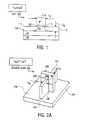
- FIG. 1illustrates a standard fully depleted silicon on insulator (SOI) transistor 100 .
- SOI transistor 100includes a single crystalline silicon substrate 102 having an insulating layer 104 , such as a buried oxide formed thereon.
- a single crystalline silicon body 106is formed on the insulating layer 104 .
- a gate dielectric layer 108is formed on the single crystalline silicon body 106 and a gate electrode 110 formed on the gate dielectric 108 .
- Source 112 and drain 114 regionsare formed in the silicon body 106 along laterally opposite sides of gate electrode 110 .
- the need for ever decreasing silicon film thickness (Tsi)makes this approach increasingly impractical.
- the thickness required of the silicon bodyis thought to need to be less than 10 nanometers, and around 6 nanometer for a 20 nanometer gate length.
- a double gate (DG) devicesuch as shown in FIGS. 2A and 2B , have been proposed to alleviate the silicon thickness issue.
- the double gate (DG) device 200includes a silicon body 202 formed on an insulating substrate 204 .
- a gate dielectric 206is formed on two sides of the silicon body 202 and a gate electrode 208 is formed adjacent to the gate dielectric 206 formed on the two sides of the silicon body 202 .
- a sufficiently thick insulating layer 209such as silicon nitride, electrically isolates the gate electrode 208 from the top of silicon body 202 .
- the most manufacturable form of the double gate (DG) device 200requires that the body 202 patterning be done with photolithography that is 0.7 ⁇ smaller than that used to pattern the gate length (Lg) of the device.
- silicon body 202requires a silicon body etch which can produce a silicon body 202 with an aspect ratio (height to width) of about 5:1
- FIG. 1is an illustration of a cross-sectional view of a depleted substrate transistor.
- FIG. 2 A and FIG. 2Billustrate a double gate depleted substrate transistor.
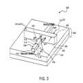
- FIG. 3is an illustration of a tri-gate transistor in accordance with an embodiment of the present invention.
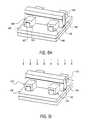
- FIG. 4Ais an illustration of a tri-gate transistor in accordance with an embodiment of the present invention.
- FIG. 4Bis an illustration of a tri-gate transistor in accordance with an embodiment of the present invention.
- FIGS. 5A-5Jillustrate methods of fabricating a tri-gate transistor in accordance with embodiments of the present invention.
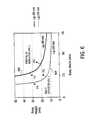
- FIG. 6is a plot which illustrates body heights and body widths which can be used to obtain partially depleted and fully depleted tri-gate transistors having gate lengths (lg) of 30 nm and 20 nm.
- FIG. 7Ais an illustration of a nonplanar transistor having a thin gate dielectric layer on the top surface of a semiconductor body and a thicker gate dielectric layer on the sidewalls of the semiconductor body.
- FIG. 7Bis an illustration of a nonplanar transistor having a single dielectric layer on the top surface of a semiconductor body and a composite dielectric layer on the sidewalls of the semiconductor body.
- FIGS. 8A-8Dillustrate a method of forming a gate dielectric layer with a greater thickness on the sidewalls of a semiconductor body than on the top surface of semiconductor body, and/or with a lower effective dielectric constant on the sidewalls of a semiconductor body than on the top surface of semiconductor body.
- FIGS. 9A-9Dillustrate a method of forming a gate dielectric layer with a greater thickness on the sidewalls of a semiconductor body than on the top surface of semiconductor body, and/or with a lower effective dielectric constant on the sidewalls of a semiconductor body than on the top surface of semiconductor body.
- the present inventionis a novel tri-gate transistor structure and its method of fabrication.
- numerous specific detailsare set forth in order to provide a thorough understanding in the present invention.
- well-known semiconductor process and manufacturing techniqueshave not been described in particular detail in order to not unnecessarily obscure the present invention.
- the present inventionis novel tri-gate transistor structure and its method of fabrication.
- the tri-gate transistoris a semiconductor on insulator (SOI) transistor.
- SOIsemiconductor on insulator
- the tri-gate transistoris ideal for use in fully depleted substrate transistor applications.
- the tri-gate transistorincludes a thin semiconductor body formed on an substrate, the substrate can be an insulating substrate or a semiconductor substrate.
- a gate dielectricis formed on the top surface and the sidewalls of the semiconductor body.
- a gate electrodeis formed on the gate dielectric on the top surface of the semiconductor body and is formed adjacent to the gate dielectric formed on the sidewalls of the semiconductor body. Source and drain regions are formed in the semiconductor body on opposite sides of the gate electrode.
- the transistoressentially has three separate channels and gates.
- the gate “width” of a transistoris equal to the sum of each of the three sides of the semiconductor body. Larger “width” transistors can be formed by connecting several tri-gate transistors together.
- the semiconductor bodycan be fully depleted when the transistor is turned “ON”, thereby enabling the formation of a fully depleted transistor with gate lengths of less than 30 nanometers without requiring the use of ultra-thin semiconductor bodies or requiring photolithographic patterning of the semiconductor bodies to dimensions less than the gate length (Lg) of the device. That is, the structure of the tri-gate transistor of the present invention enables a fully depleted transistor to be fabricated where the thickness of the semiconductor body and width of the semiconductor body are equal to the gate length of the device.
- the novel tri-gate transistor of the present inventioncan be operated in a fully depleted manner, the device is characterized by ideal (i.e., very sharp) subthreshold slope and a reduced drain induced barrier lowering (DIBL) short channel effect of less than 100 mV/V and ideally about 60 mV/V which results in a lower leakage current when the device is turned “OFF” resulting in lower power consumption.
- DIBLdrain induced barrier lowering
- Tri-gate transistor 300is formed on an substrate 302 .
- substrate 302is an insulating substrate which includes a lower monocrystalline silicon substrate 304 upon which is formed in insulating layer 306 , such as a silicon dioxide film.
- Tri-gate transistor 300can be formed on any well-known insulating substrate such as substrates formed from silicon dioxide, nitrides, oxides, and shappires.
- the substrate 302can be a semiconductor substrate, such as but not limited to monocrystalline silicon substrate and gallium arsenide substrate.
- Tri-gate transistor 300includes a semiconductor body 308 formed on insulator 306 of insulating substrate 302 .
- Semiconductor body 308can be formed of any well-known semiconductor material, such as but not limited to silicon (Si), germanium (Ge), silicon germanium (Si x Ge y ), gallium arsenide (GaAs), InSb, GaP, GaSb and carbon nanotubes.
- Semiconductor body 308can be formed of any well-known material which can be reversibly altered from an insulating state to a conductive state by applying external electrical controls.
- Semiconductor body 308is ideally a single crystalline film when the best electrical performance of transistor 300 , is desired.
- semiconductor body 308is a single crystalline film when transistor 300 is used in high performance applications, such as in a high density circuit, such as a microprocessor.
- Semiconductor body 308can be a polycrystalline film when transistor 300 is used in applications requiring less stringent performance, such as in liquid crystal displays.
- Insulator 306insulates semiconductor body 308 from monocrystalline silicon substrate 302 .
- semiconductor body 308is a single crystalline silicon film.
- Semiconductor body 308has a pair of laterally opposite sidewalls 310 and 312 separated by a distance which defines a semiconductor body width 314 . Additionally, semiconductor body 308 has a top surface 316 opposite a bottom surface 318 formed on substrate 302 .
- the distance between the top surface 316 and the bottom surface 318defines a body height 320 .
- the body height 320is substantially equal to the body width 314 .
- the body 308has a width 314 and height 320 less than 30 nanometers and ideally less than 20 nanometers.
- the body height 320is between 1 ⁇ 2 the body width 314 to 2 times the body width 314 .
- Tri-gate transistor 300has a gate dielectric layer 322 .
- Gate dielectric layer 322is formed on and around three sides of semiconductor body 308 as shown in FIG. 3 .
- Gate dielectric layer 322is formed on or adjacent to sidewall 312 , on top surface 316 and on or adjacent to sidewall 310 of body 308 as shown in FIG. 3 .
- Gate dielectric layer 322can be any well-known gate dielectric layer.
- the gate dielectric layeris a silicon dioxide (SiO 2 ), silicon oxynitride (SiO x N y ) or a silicon nitride (Si 3 N 4 ) dielectric layer.
- the gate dielectric layer 322is a silicon oxynitride film formed to a thickness of between 5-20 ⁇ .
- gate dielectric layer 322is a high K gate dielectric layer, such as a metal oxide dielectric, such as but not limited to tantalum pentaoxide (Ta 2 O 5 ), and titantium oxide (TiO 2 ).
- Gate dielectric layer 322can be other types of high K dielectric, such as but not limited to PZT.
- Tri-gate device 300has a gate electrode 324 .
- Gate electrode 324is formed on and around gate dielectric layer 322 as shown in FIG. 3 .
- Gate electrode 324is formed on or adjacent to gate dielectric 322 formed on sidewall 312 of semiconductor body 308 , is formed on gate dielectric 322 formed on the top surface 316 of semiconductor body 308 , and is formed adjacent to or on gate dielectric layer 322 formed on sidewall 310 of semiconductor body 308 .
- Gate electrode 324has a pair of laterally opposite sidewalls 326 and 328 separated by a distance which defines the gate length (Lg) 330 of transistor 300 .
- the laterally opposite sidewalls 326 and 328 of the gate electrode 324run in a direction perpendicular to the laterally opposite sidewalls 310 and 312 of semiconductor body 308 .
- Gate electrode 324can be formed of any suitable gate electrode material.
- to gate electrode 324comprises of polycrystalline silicon doped to a concentration density between 1 ⁇ 10 19 atoms/cm 3 ⁇ 1 ⁇ 10 20 atoms/cm 3 .
- the gate electrodecan be a metal gate electrode, such as but not limited to, tungsten, tantalum, titanium, and their nitrides.
- the gate electrodeis formed from a material having a mid-gap work function between 4.6-4.8 eV. It is to be appreciated, the gate electrode 324 need not necessarily be a single material and can be a composite stack of thin films, such as but not limited to a polycrystalline silicon/metal electrode or a metal/polycrystalline silicon electrode.
- Tri-gate transistor 300has a source region 330 and a drain region 332 .
- Source region 330 and drain region 332are formed in semiconductor body 308 on opposite sides of gate electrode 324 as shown in FIG. 3 .
- the source region 330 and the drain region 332are formed of the same conductivity type such as N-type or P-type conductivity.
- source region 330 and drain region 332have a doping concentration of between 1 ⁇ 10 19 , and 1 ⁇ 10 21 atoms/cm 3 .
- Source region 330 and drain region 332can be formed of uniform concentration or can include subregions of different concentrations or doping profiles such as tip regions (e.g., source/drain extensions).
- transistor 300when transistor 300 is a symmetrical transistor, source region 330 and drain region 332 will have the same doping concentration and profile. In an embodiment of the present invention when tri-gate transistor 300 is formed as an asymmetric transistor then the doping concentration and profile of the source region 330 and the drain region 332 may vary in order to obtain a particular electrical characteristic.
- the portion of semiconductor body 308 located between source region 330 and drain region 332defines the channel region 350 of transistor 300 .
- the channel region 350can also be defined as the area of the semiconductor body 308 surrounded by the gate electrode 324 .
- the source/drain regionmay extend slightly beneath the gate electrode through, for example, diffusion to define a channel region slightly smaller than the gate electrode length (Lg).
- channel region 350is intrinsic or undoped monocrystalline silicon.
- channel region 350is doped monocrystalline silicon. When channel region 350 is doped it is typically doped to a conductivity level of between 1 ⁇ 10 16 to 1 ⁇ 10 19 atoms/cm 3 .
- channel regionwhen the channel region is doped it is typically doped to the opposite conductivity type of the source region 330 and the drain region 332 .
- the channel regionwhen the source and drain regions are N-type conductivity the channel region would be doped to p type conductivity.
- the source and drain regionsare P type conductivity the channel region would be N-type conductivity.
- Channel region 350can be uniformly doped or can be doped non-uniformly or with differing concentrations to provide particular electrical and performance characteristics.
- channel regions 350can include well-known “halo” regions, if desired.
- the tri-gate transistoris characterized in having three channels and three gates, one (g 1 ) which extends between the source and drain regions on side 312 of silicon body 308 , a second (g 2 ) which extends between the source and drain regions on the top surface 316 of silicon body 308 , and the third (g 3 ) which extends between the source and drain regions on the sidewall 310 of silicon body 308 .
- the gate “width” (Gw) of transistor 300is the sum of the widths of the three channel regions.
- the gate width of transistor 300is equal to the height 320 of silicon body 308 at sidewall 310 , plus the width of silicon body of 308 at the top surface 316 , plus the height 320 of silicon body 308 at sidewall 312 .
- Larger “width” transistorscan be obtained by using multiple devices coupled together (e.g., multiple silicon bodies 308 surrounded by a single gate electrode 324 ).
- transistor 300can be operated in a fully depleted manner wherein when transistor 300 is turned “on” the channel region 350 fully depletes thereby providing the advantageous electrical characteristics and performance of a fully depleted transistor. That is, when transistor 300 is turned “ON” a depletion region is formed in channel region 350 along with an inversion layer at the surfaces of region 350 (i.e., an inversion layer is formed on the side surfaces and top surface of the semiconductor body).
- the inversion layerhas the same conductivity type as the source and drain regions and forms a conductive channel between the source and drain regions to allow current to flow therebetween.
- the depletion regiondepletes free carriers from beneath the inversion layer.
- the depletion regionextends to the bottom of channel region 350 , thus the transistor can be said to be a “fully depleted” transistor.
- Fully depleted transistorshave improved electrical performance characteristics over non-fully depleted or partially depleted transistors. For example, operating transistor 300 in a fully depleted manner, gives transistor 300 an ideal or very steep subthreshold slope.
- the tri-gate transistorcan be fabricated with very steep sub-threshold slope of less than 80 mV/decade, and ideally about 60 mV/decade even when fabricated with semiconductor body thicknesses of less than 30 nm.
- transistor 300has an improved drain induced barrier (DIBL) low in effect which provides for better “OFF” state leakage which results in lower leakage and thereby lower power consumption.
- DIBLdrain induced barrier
- the tri-gate transistor 300has a DIBL effect of less than 100 mV/V and ideally less than 40 mV/V.
- FIG. 6is an illustration of two plots 602 and 604 which set forth the body height and body width which will produce either fully depleted (F.D) or partially depleted (P.D) tri-gate transistors having gate length (Lg) of 30 nm ( 602 ) and 20 nm ( 604 ) respectively.
- the body height, body width and gate lengthare chosen to have dimensions in which a fully depleted transistor will be formed.
- the tri-gate transistorhas a body height, body width and gate length such that a partially depleted transistor is formed.
- the tri-gate transistor of the present inventioncan be said to be a nonplanar transistor because the inversion layer of the channel region 350 is formed in both the horizontal and vertical directions in semiconductor body 308 .
- the semiconductor device of the present inventioncan also be considered a nonplanar device because the electric field from the gate electrode 324 is applied from both horizontal (g 2 ) and vertical sides (g 1 and g 3 ).
- the source and drain regionscan include a silicon or other semiconductor film 410 formed on and around semiconductor body 308 as shown in FIG. 4 A.
- semiconductor film 410can be a silicon film or a silicon alloy such as silicon germanium (Si x Ge y ).
- the semiconductor film 410is a single crystalline silicon film formed of the same conductivity type as the source region 330 and drain region 332 .
- the semiconductor filmcan be a silicon alloy such as silicon germanium wherein silicon comprises approximately 1 to 99 atomic percent of the alloy.
- the semiconductor film 410need not necessarily be a single crystalline semiconductor film and in an embodiment can be a polycrystalline film.
- the semiconductor film 410is formed on the source region 330 and on the drain region 332 of semiconductor body 308 to form “raised” source and drain regions.
- Semiconductor film 410can be electrically isolated from a gate electrode 324 by a pair of dielectric sidewall spacers 420 such as silicon nitride or silicon oxide or composites thereof.
- Sidewall spacers 420run along the laterally opposite sidewalls 326 and 328 of gate electrode 324 as shown in FIG. 4A thereby isolating the semiconductor film 410 from gate electrode 324 as shown in FIG. 4 A.
- An embodiment of the present invention sidewalls spacers 420have a thickness of between 20-200 ⁇ .
- the thickness of the source and drain regionsis increased thereby reducing the source/drain contact resistance to transistor 300 and improving its electrical characteristics and performance.
- a silicide film 430such as, but not limited to, titanium silicide, nickel silicide, and cobalt silicide is formed on the source region 330 and drain region 332 .
- silicide film 430is formed on a silicon film 410 of silicon body 308 as shown in FIG. 4 A. Silicide film 430 however can also be formed directly onto the top surface 316 of silicon body 308 .
- silicide film 430can be formed on silicon body 308 by first forming a silicon film such as an undoped silicon film and a silicon body and then completely consuming the silicon film during the silicide process.
- Dielectric spacers 420enables silicide film 430 to be formed on semiconductor body 308 or silicon film 410 in a self-aligned process (i.e., a salicide process).
- a semiconductor or silicon film 440can also be formed on the top of gate electrode 324 as can a silicide film 450 on the top surface gate electrode 325 as can be a silicide film 450 .
- Silicide film 450 and silicon film 440are typically formed at the same time as silicide film 430 and silicon film 420 on silicon body 308 .
- the formation of a silicon film 440 on silicide film 450 on the gate electrodereduces the contact resistance to the gate thereby improving the electrical performance of transistor 300 .
- transistor 300can include an additional or multiple semiconductor bodies or fingers 308 as shown in FIG. 4 B.
- Each semiconductor body 308has a gate dielectric layer 322 formed on its top surface and sidewalls as shown in FIG. 4 B.
- Gate electrode 324is formed on and adjacent to each gate dielectric 322 on each of the semiconductor bodies 308 .
- Each semiconductor body 308also includes a source region 330 and a drain region 332 formed in the semiconductor body 308 on opposite sides of gate electrode 324 as shown in FIG. 4 B.
- each semiconductor body 308is formed with the same width and height (thickness) as the other semiconductor bodies 308 .
- each source regions 330 and drain regions 332 of the semiconductor bodies 308are electrically coupled together by the semiconductor material used to form semiconductor body 308 to form a source landing pad 460 and a drain landing pad 480 as shown in FIG. 4 B.
- the source regions 330 and drain regions 332can be coupled together by higher levels of metalization (e.g., metal 1, metal 2, metal 3 . . . ) used to electrically interconnect various transistors 300 together into functional circuits.
- the gate width of transistor 300 as shown in FIG. 4Bwould be equal to the sum of the gate width created by each of the semiconductor bodies 308 . In this way, the tri-gate transistor 300 can be formed with any gate width desired.
- FIGS. 5A-5JA method of fabricating a tri-gate transistor in accordance with embodiments of the present invention is illustrated in FIGS. 5A-5J .
- the fabrication of a tri-gate transistorbegins with substrate 502 .
- a silicon or semiconductor film 508is formed on substrate 502 as shown in FIG. 5 A.
- the substrate 502is an insulating substrate, such as shown in FIG. 5 A.
- insulating substrate 502includes a lower monocrystalline silicon substrate 504 and a top insulating layer 506 , such as a silicon dioxide film or silicon nitride film. Insulating layer 506 isolates semiconductor film 508 from substrate 504 , and in embodiment is formed to a thickness between 200-2000 ⁇ .
- Insulating layer 506is sometimes referred to as a “buried oxide” layer.
- a silicon or semiconductor film 508is formed on an insulating substrate 502 , a silicon or semiconductor on insulating (SOI) substrate 500 is created.
- the substrate 502can be a semiconductor substrate, such as but not limited to a silicon monocrystalline substrate and a gallium arsenide substrate.
- semiconductor film 508is ideally a silicon film, in other embodiments it can be other types of semiconductor films, such as but not limited to germanium (Ge), a silicon germanium alloy (Si x Ge y ), gallium arsenide (GaAs), InSb, GaP, GaSb, as well as carbon nanotubes.
- semiconductor film 508is an intrinsic (i.e., undoped) silicon film.
- semiconductor film 508is doped to a p type or n type conductivity with a concentration level between 1 ⁇ 10 16 ⁇ 1 ⁇ 10 19 atoms/cm 3 .
- Semiconductor film 508can be insitu doped (i.e., doped while it is deposited) or doped after it is formed on substrate 502 by for example ion-implantation. Doping after formation enables both PMOS and NMOS tri-gate devices to be fabricated easily on the same insulating substrate. The doping level of the semiconductor body at this point determines the doping level of the channel region of the device.
- Semiconductor film 508is formed to a thickness which is approximately equal to the height desired for the subsequently formed semiconductor body or bodies of the fabricated tri-gate transistor. In an embodiment of the present invention, semiconductor film 508 has a thickness or height 509 of less than 30 nanometers and ideally less than 20 nanometers. In an embodiment of the present invention, semiconductor film 508 is formed to the thickness approximately equal to the gate “length” desired of the fabricated tri-gate transistor. In an embodiment of the present invention, semiconductor film 508 is formed thicker than desired gate length of the device. In an embodiment of the present invention, semiconductor film 580 is formed to a thickness which will enable the fabricated tri-gate transistor to be operated in a fully depleted manner for its designed gate length (Lg).
- Lggate length
- Semiconductor film 508can be formed on insulating substrate 502 in any well-known method.
- a silicon on insulator substrateknown as the SIMOX technique
- oxygen atomsare implanted at a high dose into a single crystalline silicon substrate and then anneal to form the buried oxide 506 within the substrate.
- the portion of the single crystalline silicon substrate above the buried oxidebecomes the silicon film 508 .
- Another technique currently used to form SOI substratesis an epitaxial silicon film transfer technique which is generally referred to as bonded SOI.
- bonded SOIIn this technique a first silicon wafer has a thin oxide grown on its surface that will later serve as the buried oxide 506 in the SOI structure.
- a high dose hydrogen implantis made into the first silicon wafer to form a high stress region below the silicon surface of the first wafer.
- This first waferis then flipped over and bonded to the surface of a second silicon wafer.
- the first waferis then cleaved along the high stress plain created by the hydrogen implant. This results in a SOI structure with a thin silicon layer on top, the buried oxide underneath all on top of the single crystalline silicon substrate.
- Well-known smoothing techniquessuch as HC smoothing or chemical mechanical polishing (CMP) can be used to smooth the top surface of semiconductor film 508 to its desired thickness.
- isolation regionscan be formed into SOI substrate 500 in order to isolate the various transistors to be formed therein from one another. Isolation regions can be formed by etching away portions of the substrate film 508 surrounding a tri-gate transistor, by for example well-known photolithographic and etching techniques, and then back filling the etched regions with an insulating film, such as SiO 2 .
- a photoresist mask 510is formed on semiconductor film 508 as shown in FIG. 5 B.
- the photoresist mask 510contains a pattern or plurality of patterns 512 defining locations where semiconductor bodies or fins will be subsequently formed in the semiconductor film 508 .
- the photoresist pattern 512defines the width 518 desired of the subsequently formed semiconductor bodies or fins of the tri-gate transistor.
- the pattern 512define fins or bodies having a width 518 which is equal to or greater than the width desired of the gate length (Lg) of the fabricated transistor.
- the semiconductor bodies or finswill have a width 518 less than or equal to 30 nanometers and ideally less than or equal to 20 nanometers.
- the patterns 512 for the semiconductor bodies or finshave a width 518 approximately equal to the silicon body height 509 .
- the photoresist patterns 512have a width 518 which is between 1 ⁇ 2 the semiconductor body height 509 and two times the semiconductor body height 509 .
- the photoresist mask 510can also include patterns 514 and 516 for defining locations where source landing pads and drain landing pads, respectively, are to be formed.
- the landing padscan be used to connect together the various source regions and to connect together the various drain regions of the fabricated transistor.
- the photoresist mask 510can be formed by well-known photolithographic techniques including masking, exposing, and developing a blanket deposited photoresist film.
- semiconductor film 508is etched in alignment with photoresist mask 510 to form one or more silicon bodies or fins and source and drain landing pads (if desired) as shown in FIG. 5 C.
- Semiconductor film 508is etched until the underlying buried oxide layer 506 is exposed.
- Well-known semiconductor etching techniquessuch as anisotropic plasma etching or reactive ion etching can be used to etch semiconductor film 508 in alignment with mask 510 as shown in FIG. 5 C.
- semiconductor film 508is etched to form semiconductor bodies or fins 520 (and source/drain landing pads 522 and 524 , if desired)
- the photoresist maskis removed by well-known techniques, such as by chemical stripping and O 2 ashing, to produce the substrate shown in FIG. 5 D.
- a gate dielectric layer 526is formed on and around each semiconductor body 520 . That is, a gate dielectric layer 526 is formed on the top surface 527 of each of the semiconductor bodies 520 as well as on the laterally opposite sidewalls 528 and 529 of each of the semiconductor bodies 520 .
- the gate dielectriccan be a deposited dielectric or a grown dielectric.
- the gate dielectric layer 526is a silicon dioxide dielectric film grown with a dry/wet oxidation process. In an embodiment of the present invention, the silicon oxide film is grown to a thickness of between 5-15 ⁇ .
- the gate dielectric film 526is a deposited dielectric, such as but not limited to a high dielectric constant film, such as metal oxide dielectric, such as tantalum pentaoxide (Ta 2 O 5 ) and titanium oxide (TiO2) or other high-K dielectrics, such as PZT and BST.
- a high dielectric constant filmcan be formed by any well-known technique, such as by chemical vapor deposition (CVD).
- a gate electrode 530is formed.
- the gate electrode 530is formed on the gate dielectric layer 526 formed on the top surface 527 of each of the semiconductor bodies 520 and is formed on or adjacent to the gate dielectric 526 formed on or adjacent to the sidewalls 528 and 529 of each of the semiconductor bodies as shown in FIG. 5 E.
- the gale electrode 530has a top surface 532 opposite of bottom surface formed on the insulating substrate 502 and has a pair of laterally opposite sidewalls 534 and 536 . The distance between the laterally opposite sidewalls 534 and 536 define the gate length (Lg) 538 of the tri-gate transistor.
- Gate electrode 530can be formed by blanket depositing a suitable gate electrode material over the substrate shown in FIG.
- the gate electrodecan be formed to a thickness 533 between 200-3000 ⁇ . In an embodiment the gate electrode has a thickness or height 533 of at least three times the height 509 of semiconductor bodies 520 .
- the gate electrode materialis then patterned with well-known photolithography and etching techniques to form gate electrode 530 from the gate electrode material.
- the gate electrode materialcomprises polycrystalline silicon.
- the gate electrode materialcomprises a polycrystalline silicon germanium alloy.
- the gate electrode materialcan comprise a metal film, such as tungsten, tantalum, and their nitrides.
- Gate electrode 530can be formed by well-known techniques, such as by blanket depositing a gate electrode material over the substrate of FIG.
- the photolithography process used to define gate electrode 530utilizes the minimum or smallest dimension lithography process used to fabricate the tri-gate transistor. (That is, in an embodiment of the present invention, the gate length (Lg) 538 of gate electrode 530 has a minimum feature dimension of the transistor defined by photolithography.) In an embodiment of the present invention, the gate length 538 is less than or equal to 30 nanometers and ideally less than or equal to 20 nanometers.
- source and drain regions for the transistorare formed in semiconductor body 520 on opposite sides of gate electrode 530 .
- the source and drain regionsinclude tip or source/drain extension regions.
- Source and drain extension regions 540 and 542can be formed by placing dopants 544 into semiconductor bodies 520 on both sides 532 , 534 of gate electrode 530 in order to form tip regions 540 and 542 as shown in FIG. 5 F.
- Source and drain landing pads 522 and 524are not shown in FIGS. 5F-5J to better illustrate aspects of the present invention. If source and drain landing pads 522 and 524 are utilized, they may be doped at this time also.
- the semiconductor fins or bodies 520are doped to a p type conductivity and to a concentration between 1 ⁇ 10 20 ⁇ 1 ⁇ 10 21 atoms/cm 3 .
- the semiconductor fins or bodies 520is doped with n type conductivity ions to a concentration between 1 ⁇ 10 20 ⁇ 1 ⁇ 10 21 atoms/cm 3 .
- the silicon filmsare doped by ion-implantation. In an embodiment of the present invention, the ion-implantation occurs in a vertical direction (i.e., a direction perpendicular to substrate 500 ) as shown in FIG. 5 F.
- gate electrode 530When gate electrode 530 is a polysilicon gate electrode, it can be doped during the ion-implantation process. Gate electrode 530 acts as a mask to prevent the ion-implantation step from doping the channel region(s) 548 of the tri-gate transistor. The channel region 548 is the portion of the silicon body 520 located beneath or surrounded by the gate electrode 530 . If gate electrode 530 is a metal electrode, a dielectric hard mask maybe used to block the doping during the ion-implantation process. In other embodiments, other methods, such as solid source diffusion, may be used to dope the semiconductor body to form source and drain extensions.
- Halo regionscan be formed in silicon body prior to the formation of a source/drain regions or source/drain extension regions.
- Halo regionsare doped regions formed in the channel region 548 of the device and are of the same conductivity but of a slightly higher concentration than the doping of the channel region of the device.
- Halo regionscan be formed by ion-implantating dopants beneath the gate electrode by utilizing large angled ion-implantation techniques.
- the substrate shown in FIG. 5Fcan be further processed to form additional features, such as heavily doped source/drain contact regions, deposited silicon on the source and drain regions as well as the gate electrode, and the formation of silicide on the source/drain contact regions as well as on the gate electrode.
- dielectric sidewall spacers 550can be formed on the sidewalls of the gate electrode. Sidewall spacers can be utilized to offset heavy source/drain contact implants, can be used to isolate source/drain regions from the gate electrode during a selective silicon deposition processes and can be used in a salicide process to form silicide on the source and drain regions as well as on the gate electrode. Spacers can be formed by blanket depositing a conformal dielectric film 550 , such as but not limited to silicon nitride, silicon oxide, silicon oxynitride or combination thereof over the substrate 500 of FIG. 5 F.
- Dielectric filmis deposited in a conformal manner so that it forms to substantially equal heights on vertical surfaces, such as sidewalls 534 and 536 of gate electrode 530 as well as on horizontal surfaces, such as on the top 526 of silicon film 520 and the top of gate electrode 530 .
- the dielectric filmis a silicon nitride film formed by a hot wall low-pressure chemical vapor deposition (LPCVD) process.
- LPCVDhot wall low-pressure chemical vapor deposition
- the deposited thickness of the dielectric filmdetermines the width or thickness of the formed spacers.
- the dielectric filmis formed to a thickness between 20-200 ⁇ .
- the dielectric filmis anisotropically etched by for example plasma etching or reactive ion etching to form sidewall spacers 550 .
- the anisotropic etch of dielectric filmremoves the dielectric film from horizontal surfaces, such as the top of gate electrode 530 (as well as the top of landing pads 522 and 524 if used) and leaves dielectric sidewall spacers adjacent to vertical surfaces, such as sidewalls 534 and 536 of gate electrode 530 .
- the etchis continued for a sufficient period of time to remove the dielectric film from all horizontal surfaces.
- an over etchis utilized so that the spacer material on the sidewalls of the semiconductor bodies 520 is removed as shown in FIG. 5 G.
- the resultis the formation of sidewall spacers 550 which run along and adjacent to sidewall 532 and 534 of gate electrode 530 as shown in FIG. 5 H.
- a semiconductor film 560can be formed on the exposed surfaces of semiconductor body 520 (as well as on landing pads 522 and 524 ) as shown in FIG. 5 H. Additionally, if desired, a semiconductor film 562 can be formed on the top of gate electrode 530 .
- the semiconductor filmcan be a single crystalline film or a polycrystalline film.
- semiconductor film 560is an epitaxial (single crystalline) silicon film.
- the silicon film 560is formed by a selective deposition process whereby silicon is formed only on exposed regions which contain silicon, such as the exposed top surface 527 and sidewalls 528 and 529 of silicon body 520 .
- a silicon film 560is formed to a thickness between 50-500 ⁇ .
- the silicon filmis formed to a thickness sufficient to provide enough silicon to be used or consumed during the formation of a silicide film on the source and drain regions.
- the silicon filmcan be insitu doped (i.e., doped during deposition) or subsequently doped by for example ion-implantation or solid source diffusion.
- the silicon filmis doped to the conductivity type desired for the source and drain regions of the device.
- the deposited silicon film 560 and 562are intrinsic silicon films (i.e., undoped silicon films).
- the deposition of semiconductor film 560forms raised source and drain regions which improves the parasitics of the device.
- the deposited silicon film 560 and 562are doped by ion-implantation utilizing a vertical ion-implantation angle.
- the ion-implantation processdopes the deposited silicon film 560 and the silicon body 520 located underneath to a concentration between 1 ⁇ 10 20 ⁇ 1 ⁇ 10 21 atoms/cm 3 to form a source contact region 570 and a drain contact region 572 .
- Sidewall spacers 550offset the source/drain contact implantation step and define the tips regions as a region of the doped silicon body beneath sidewall spacer 550 .
- the above referenced processforms source regions 570 and drain regions 572 which each comprise a tip region and a contact region.
- the tip regionis the region of the silicon body 520 located beneath sidewall spacers 555 .
- the contact regionsare the regions of the silicon body and deposited silicon film which are adjacent to the outside edges of the sidewall spacers 550 . Additionally, the source/drain contact regions include the source and drain landing pads 522 and 524 when utilized.
- a refractory metal silicide 580can be formed on the source and drain contact regions as well as on the top of gate electrode 530 (or silicon film 562 ) as shown in FIG. 5J.
- a refractory metal silicide film 580can be formed with a self-aligned process, such as a salicide process.
- a refractory metal filmsuch as titanium, tungsten, nickel, cobalt or alike to blanket deposited over the substrate of FIG. 5 J.
- the substrateis then heated to a suitable temperature to cause the refractory metal film to react with silicon portion of substrate 500 , such as silicon film 560 formed on the silicon bodies and silicon film 562 formed on the gate electrodes in order to form a refractory metal silicide.
- silicon portion of substrate 500such as silicon film 560 formed on the silicon bodies and silicon film 562 formed on the gate electrodes in order to form a refractory metal silicide.
- Locations where silicon is unavailable to reactsuch as dielectric spacers 555 and exposed portions of buried oxide 506 , do not react and remain as refractory metal.
- a selective etchsuch as a wet etch can then be utilized to remove the unreacted refractory metal and leave the refractory metal silicide on the contact areas. In this way, a metal silicide film can be self-aligned to the contact regions of a tri-gate transistor. This completes the fabrication of a tri-gate transistor in accordance with the present invention.
- the gate dielectric layeris formed such that the sidewall capacitance of the trigate or nonplanar transistor is reduced. Applicant has discovered that the majority of the current conduction of a trigate or nonplanar transistor occurs at the corner of the semiconductor body between the top surface and the laterally opposite sidewalls of the semiconductor body. Because little current is conducted on the sidewalls, it desirable to reduce the gate capacitance associated with the sidewalls to thereby improve the device current per unit capacitance of the sidewalls. Accordingly, in an embodiment of the present invention the gate dielectric is fabricated in such a manner so that the gate dielectric layer on the sidewalls of the semiconductor body provides a lower gate capacitance per gate width than does the gate dielectric layer on the top surface of the semiconductor body.
- a lower gate capacitance per gate width on the sidewalls of the semiconductor body as compared to the top surfacecan be achieved by, for example, making the gate dielectric layer thicker on the sidewalls of the semiconductor body as compared to the top surface of the semiconductor body and/or making the effective dielectric constant (K effective) of the gate dielectric layer on the sidewalls lower than the effective dielectric constant of the gate dielectric layer on the top surface of a semiconductor body.
- a semiconductor body 702 having a top surface 704 and a pair laterally opposite sidewalls 706is formed on an insulating substrate 700 .
- a gate dielectric layer 710is formed on and around the semiconductor body 702 as shown in FIG. 7 A.
- the gate dielectric layer 710includes a first portion 712 formed on the top surface 704 of the semiconductor body 702 and a second portion 714 formed on or directly adjacent to the sidewalls 706 of semiconductor body 702 .
- the gate dielectric layer 714 on the sidewalls 706 of the semiconductor body 702is thicker than the gate dielectric layer 712 on the top surface 704 of the semiconductor body 702 .
- the gate dielectric layer 714 on the sidewalls of the semiconductor body 702is at least 1.3 times the thickness of the gate dielectric layer 712 formed on the top surface 704 of the semiconductor body 702 .
- a gate electrode 718is formed on first dielectric portion 712 and on or adjacent to the second dielectric portion 714 , as shown in FIG. 7 A.
- the gate dielectric layer 724 on the sidewalls 706 of the semiconductor body 702is a composite gate dielectric which comprises a first dielectric layer 720 formed on or directly adjacent to the sidewalls 706 of the semiconductor body 702 and a second dielectric layer 722 formed on or directly adjacent to the first dielectric layer 720 .
- the second dielectric 722is also formed directly on the top surface 704 of the semiconductor body 702 , as shown in FIG. 7 B.
- the second dielectric layer 722is a deposited high dielectric constant (high K) film.
- a high dielectric constant filmtypically has a dielectric constant of greater than 9.0 and ideally greater than 20.
- a high dielectric constant filmcan be a metal oxide dielectric, such as but not limited to tantalum pentaoxide (Ta 2 O 5 ), titanium oxide, hafnium oxide, zirconium oxide, and aluminum oxide and various silicates.
- the second dielectric layer 722can be these or other well known high dielectric constant films, such as lead zirconate titanate (PZT) or barium strontium titatanate (BST).
- PZTlead zirconate titanate
- BSTbarium strontium titatanate
- Utilizing a high dielectric constant filmenables a gate dielectric to be formed relatively thick between 20-3000 ⁇ and ideally about 200 ⁇ for a high dielectric constant (K>100) material.
- a thick gate dielectric layerhelps block gate leakage current of the device.
- a gate electrode 740is formed on second dielectric 722 on the top surface 704 of body 702 and on or adjacent to the composite dielectric 724 adjacent to the sidewalls 706 of body
- the first dielectric layer 720 formed on the sidewalls 706 of the semiconductor body 702is a grown dielectric layer, such as a silicon dioxide or silicon oxynitride film.
- the first dielectric layer 720has a dielectric constant (K) less than the dielectric constant of the second dielectric layer 722 .
- K effectivethe effective dielectric constant of the composite dielectric layer 724 formed on and adjacent to the sidewalls 706 of the semiconductor body 702 will be lower than the dielectric constant of the dielectric film 712 formed on the top surface 704 of the semiconductor body 702 .
- the composite dielectric 714comprises a first dielectric layer 720 which has a relatively low dielectric constant (e.g., K less than 8), and a second dielectric 722 which has a high dielectric constant (e.g., K greater than 20), the effective dielectric constant (K effective) of the composite film 724 will be less than the dielectric constant of the high dielectric film 722 formed alone on the top surface. In this way, there is less gate capacitance associated with the sidewalls 706 than the top surface 704 .
- K effectivethe effective dielectric constant
- the gate capacitance associated with the sidewallsis even further decreased.
- the first dielectric layer 720is formed on the sidewalls 706 of the semiconductor body 702 below the corners 730 of the semiconductor body between the top surface 704 and the sidewalls 706 .
- a nonplanar devicesuch as the trigate device
- the majority of the current flowoccurs in the vicinity of corners 730 of the semiconductor body 702 .
- the corners 730are rounded which can help improve device performance and/or reliability.
- One method of forming a gate dielectric film 710 with a different thickness on the top surface 704 than on the sidewalls 706is to provide an epitaxial silicon body or fin 702 which contains sidewalls 706 which have a (110) crystal orientation and a top surface 704 which has a (100) crystal orientation.
- the fins or silicon body 702can then be thermally oxidized by any well-known process, such as by a wet oxidation (H 2 O) or a combination dry/wet oxidation to form the dielectric film 710 .
- the thermal oxidation of the silicon body 702will result in a thicker oxide on the sidewalls 706 than on the top surface 704 of the semiconductor body.
- the differential oxidation rate due to the different crystal orientations of the sidewalls and top surfaceresults in a thermally grown oxide having a sidewall to top surface thickness ratio of approximately equal to or greater than 1.3.
- the gate dielectric film 712 on the top surface of the semiconductor body 702has a thickness of about 15 ⁇ while the thickness on the sidewalls of the silicon body 702 is approximately 27 ⁇ .
- the differential oxide growth rate between the top surface 704 and the sidewalls 706can be enhanced by incorporating an oxidation resistance or impeding impurity species, such as nitrogen, into the top surface 704 of the silicon body 702 .
- an oxidation resistance or impeding impurity speciessuch as nitrogen
- Implanting nitrogen into the top surface 704impedes or slows the oxidation rate of the top surface of the silicon body thereby providing a larger differential oxide growth rate between the sidewalls and the top surface resulting in a thicker gate dielectric on the sidewalls 706 as compared to the top surface 704 .
- incorporating nitrogen into the top surfacecan result in the formation of a silicon oxynitride film on the top surface 704 of the silicon body 702 .
- a silicon oxynitride filmhas a higher dielectric constant than does a pure silicon oxide film resulting in a greater difference between the gate capacitance per gate width associated with the sidewalls as compared to the gate capacitance of the top surface.
- the sidewalls 706 of semiconductor body 702can be altered to enhance the oxidation rate of the sidewalls 706 as compared to the top surface 704 .
- the sidewalls 706can be exposed to a sputter etch process prior to oxidation in order to roughen their surface to provide a greater surface area to enhance the oxidation rate of the sidewalls.
- a roughening processcan occur, for example, after etching the silicon body 520 and prior to removing the photoresist mask 510 as shown in FIG. 5 A.
- a hard maskcan be formed on the top surface of the semiconductor body to protect the top surface from the roughening process to enable the differential oxide growth.
- FIGS. 8A-8Dillustrate a method of forming a gate dielectric layer with a greater thickness on the sidewalls of a semiconductor body than on the top surface of a semiconductor body, and/or with a lower effective dielectric constant on the sidewalls of a semiconductor body than on the top surface of a semiconductor body.
- the process, as set forth in FIG. 8A-8Dcan begin after the formation of a semiconductor body or fins as illustrated in FIG. 5 D.
- the first step as shown in FIG. 8Ais to form a first dielectric layer 814 on the top surface 804 of a semiconductor body 802 and on or directly adjacent to a pair of laterally opposite sidewalls 806 of semiconductor body 802 formed on an insulating substrate 800 .
- the first dielectric layer 814is a thermally grown silicon dioxide or silicon oxynitride dielectric layer.
- semiconductor body 802is a silicon monocrystalline film having sidewalls with a (110) crystal orientation and a top surface with a (100)
- a thermal oxidation processwill grow a thicker oxide on the sidewalls 806 than on the top surface 804 of the semiconductor body as shown in FIG. 8 A.
- any well known thermal oxidation processcan be used to form the thermally grown silicon oxide or silicon oxynitride film 814 .
- the corners 830are rounded by the oxidation process. Rounded corners 830 improves the reliability and performance of the fabrication transistor.
- a thermal oxide having a thickness of at least 10 ⁇(approximately 2-3 monolayers) can be formed on the top surface 804 of the semiconductor body 802 and on the sidewalls 806 on the semiconductor body 802 .
- the first dielectric 814is ideally a grown dielectric, the first dielectric layer 814 can be a deposited dielectric, if desired.
- the first dielectric layer 814is formed of a material and to a thickness sufficient to make the sidewall gate capacitance per gate width approximately 30% less than the gate capacitance on the top surface of the semiconductor body.
- the first portion of the dielectric film 814 formed on the top surface 804 of semiconductor body 802is removed as shown in FIG. 8 B.
- the portion of the first gate dielectric layer 814 covering the corners 830 of the semiconductor body 802is also removed.
- the portion of the first dielectric layer 814 formed on the top surface of the semiconductor body 802is removed utilizing an anisotropic etching process. Such an etching process will remove the dielectric film 814 from horizontal surfaces, such as the top surface 804 of semiconductor body 802 while leaving the first gate dielectric layer 814 on the sidewalls 806 as shown in FIG. 8 B.
- An over etching processcan be utilized to recess the gate dielectric layer 814 on the sidewalls 806 so that the gate dielectric layer 814 covering corners 830 is also removed as shown in FIG. 8 B.
- Any well known anisotropic etching techniquecan be utilized, such as reactive ion etching (RIE).
- a second dielectric layer 820is formed directly onto the top surface 804 of semiconductor body 802 as well as on or directly adjacent to first dielectric layer 814 formed on the sidewalls 806 of semiconductor body 802 as shown in FIG. 8 C.
- the second dielectric layer 820is a deposited high K dielectric film, such as but not limited to PZT, BST, tantalum pentaoxide, hafnium oxide, zirconium oxide and aluminum oxide and various silicates. Any well known and suitable technique can be utilized to deposit second dielectric layer 820 including but not limited to chemical vapor deposition (CVD), atomic layer deposition (ALD), and sputtering (PVD).
- the second deposited dielectric layer 820is formed to a thickness between 20-3000 ⁇ depending on the targeted dielectric thickness.
- a gate electrode 840is formed on gate dielectric layer 820 formed on the top surface 804 of semiconductor body 802 as well as formed directly adjacent to second gate dielectric layer 820 formed adjacent to gate dielectric layer 814 formed on sidewalls 806 of semiconductor body 802 as described above. Processing of the fabricated device can then continue as set forth in FIGS. 5F-5J as described above. Although the process shown in FIGS.
- FIGS. 8A-8Dillustrate a gate dielectric formed from a composite film 814 and 820 on the sidewalls 806 and a single dielectric film 820 on the top surface 804
- the above referenced processcan be utilized to form three or more films on the sidewalls and one or more films on the top surface in order to obtain and achieve a desired thickness differential and/or effective gate dielectric constant differential between the sidewall gate dielectric and top gate dielectric.
- FIGS. 9A-9Dillustrate another method of forming a gate dielectric layer with a greater thickness on the sidewalls than on the top surface of a semiconductor body, and/or with gate dielectric layer with a lower effective dielectric constant on the sidewalls than on the top surface of the semiconductor body.
- an oxidation resistant mask 908is formed on the top surface 904 of a semiconductor body 902 having a top surface and laterally opposite sidewalls 906 .
- the oxidation resistant mask 908can be formed on the top surface of the semiconductor body by, for example, forming a blanket deposition of an oxidation resistant mask film, such as a silicon nitride or silicon oxynitride film, over the semiconductor film 508 shown in FIG. 5 A.
- the oxidation resistant filmcan then be patterned along with the semiconductor thin film 508 when it is patterned into semiconductor body or fins as shown in FIG. 5 C.
- the oxidation resistant maskis formed of a material and to a thickness sufficient to prevent the underlying top surface 904 of the semiconductor body 902 from oxidizing during a thermal oxidation process.
- the oxidation resistant maskis a silicon nitride or silicon oxynitride film formed to a thickness between 30-1000 ⁇ .
- the semiconductor bodyis exposed to a thermally oxidizing ambient in order to thermally grow a silicon dioxide film 910 on the sidewalls 906 of the semiconductor body 902 .
- the oxidation resistant mask 908prevents the top surface 904 of the semiconductor body 902 from being oxidized.
- Any well known thermal oxidation processsuch as a wet oxidation or a dry/wet oxidation may be utilized to thermally grow a silicon oxide dielectric layer 910 as shown in FIG. 9 B.
- gate dielectric layer 910is grown to a thickness of approximately 10 ⁇ or 2-3 monolayers.
- the thermally grown gate dielectric layer 910is formed to a thickness sufficient to make the sidewall gate capacitance approximately 30% less than the gate capacitance on the top surface of the semiconductor body.
- the hard mask film 908is removed with a selective etch which is selective to the thermally grown silicon dioxide dielectric film 910 .
- a phosphoric acid wet etchcan be utilized to remove a hard mask 908 and thereby expose the top surface 904 of semiconductor body 902 without substantially etching sidewall gate oxide dielectric 910 .
- a second dielectric layer 912is deposited directly onto the top surface 904 of semiconductor body 902 as well as onto or directly adjacent to the dielectric layer 910 on the sidewalls 906 of semiconductor body 902 .
- the deposited dielectric layer 912is a high K dielectric film, such as but not limited to PZT, BST, tantalum pentaoxide, hafnium oxide, zirconium oxide and aluminum oxide and various silicates. Any well known technique can be utilized to deposit dielectric layer 912 , such as but not limited to chemical vapor deposition, atomic layer deposition, and sputtering.
- the deposited dielectric layerwill typically be formed in a conformal manner wherein the thickness on vertical surfaces, such as sidewalls 906 will be similar to the thickness on horizontal surfaces, such as top surface 904 .
- the second dielectriccan be deposited to a thickness between 20-3000 ⁇ depending on the targeted dielectric thickness.
- a gate electrode 940is formed above or directly on top of gate dielectric body 912 formed on the top surface 904 of semiconductor body 902 as well as on or directly adjacent to dielectric layer 912 formed on dielectric 910 on sidewalls 906 of semiconductor body 902 as shown in FIG. 9 D and described above.
- the nonplanar or trigate semiconductor devicecan be processed as set forth in FIGS. 5F-5J to complete fabrication of the semiconductor device.
Landscapes
- Engineering & Computer Science (AREA)
- Chemical & Material Sciences (AREA)
- Nanotechnology (AREA)
- Materials Engineering (AREA)
- Physics & Mathematics (AREA)
- Mathematical Physics (AREA)
- Theoretical Computer Science (AREA)
- Crystallography & Structural Chemistry (AREA)
- Thin Film Transistor (AREA)
- Insulated Gate Type Field-Effect Transistor (AREA)
- Electrodes Of Semiconductors (AREA)
- Carbon And Carbon Compounds (AREA)
Abstract
Description
This is a Continuation-In-Part of prior application Ser. No. 10/227,068 filed on Aug. 23, 2002.
1. Field of the Invention
The present invention relates to the field of semiconductor integrated circuit manufacturing, and more particularly to a tri-gate fully depleted substrate transistor and its methods of fabrication.
2. Discussion of Related Art
In order to increase device performance, silicon on insulator (SOI) transistors have been proposed for the fabrication of modern integrated circuits.FIG. 1 illustrates a standard fully depleted silicon on insulator (SOI)transistor 100.SOI transistor 100 includes a singlecrystalline silicon substrate 102 having aninsulating layer 104, such as a buried oxide formed thereon. A singlecrystalline silicon body 106 is formed on theinsulating layer 104. A gatedielectric layer 108 is formed on the singlecrystalline silicon body 106 and agate electrode 110 formed on the gate dielectric108.Source 112 anddrain 114 regions are formed in thesilicon body 106 along laterally opposite sides ofgate electrode 110.
Fully depleted SOI have been proposed as a transistor structure to take advantage of ideal sub-threshold gradients for optimized on current/off current ratios. In order to achieve ideal subthreshold gradients withtransistor 100, the thickness of thesilicon body 106 must be about ⅓ the size of the gate length (Lg) of the transistor or Tsi=Lg/3. However, as gate lengths scale especially as they approach 30 nm, the need for ever decreasing silicon film thickness (Tsi) makes this approach increasingly impractical. At 30 nanometer gate length, the thickness required of the silicon body is thought to need to be less than 10 nanometers, and around 6 nanometer for a 20 nanometer gate length. The fabrication of thin silicon films with thicknesses of less than 10 nanometers, is considered to be extremely difficult. On one hand, obtaining wafer uniformity on the order of one nanometer is a difficult challenge. On the other hand, to be able to contact these thin films to form raised source/drain regions to decrease junction resistance, becomes almost impossible since the thin silicon layer in the source/drain regions becomes consumed during the gate etch and various cleans following the gate etch and spacer etch leavinginsufficient silicon 106 for silicon to grow on.
A double gate (DG) device, such as shown inFIGS. 2A and 2B , have been proposed to alleviate the silicon thickness issue. The double gate (DG)device 200 includes asilicon body 202 formed on aninsulating substrate 204. A gate dielectric206 is formed on two sides of thesilicon body 202 and agate electrode 208 is formed adjacent to the gate dielectric206 formed on the two sides of thesilicon body 202. A sufficiently thickinsulating layer 209, such as silicon nitride, electrically isolates thegate electrode 208 from the top ofsilicon body 202.
Double gate (DG)device 200 essentially has two gates, one on: either side of the channel of the device. Because thedouble gate device 200 has a gate on each side of the channel, thickness (Tsi) of the silicon body can be double that of a single gate device and still obtain a fully depleted transistor operation. That is, with a double gate device200 a fully depleted transistor can be formed where Tsi=(2×Lg)/3. The most manufacturable form of the double gate (DG)device 200, however, requires that thebody 202 patterning be done with photolithography that is 0.7×smaller than that used to pattern the gate length (Lg) of the device. In order to obtain high density integrated circuits, it is generally desirable to have the most aggressive lithography occur with respect to the gate length (Lg) of thegate electrode 208. Although, double gate structures double the thickness of the silicon film (since there now is a gate on either side of the channel) these structures, however, are hideously difficult to fabricate. For example,silicon body 202 requires a silicon body etch which can produce asilicon body 202 with an aspect ratio (height to width) of about 5:1
FIG.2A andFIG. 2B illustrate a double gate depleted substrate transistor.
The present invention is a novel tri-gate transistor structure and its method of fabrication. In the following description numerous specific details are set forth in order to provide a thorough understanding in the present invention. In other instances, well-known semiconductor process and manufacturing techniques have not been described in particular detail in order to not unnecessarily obscure the present invention.
The present invention is novel tri-gate transistor structure and its method of fabrication. In an embodiment of the present invention, the tri-gate transistor is a semiconductor on insulator (SOI) transistor. The tri-gate transistor is ideal for use in fully depleted substrate transistor applications. The tri-gate transistor includes a thin semiconductor body formed on an substrate, the substrate can be an insulating substrate or a semiconductor substrate. A gate dielectric is formed on the top surface and the sidewalls of the semiconductor body. A gate electrode is formed on the gate dielectric on the top surface of the semiconductor body and is formed adjacent to the gate dielectric formed on the sidewalls of the semiconductor body. Source and drain regions are formed in the semiconductor body on opposite sides of the gate electrode. Because the gate electrode and the gate dielectric surround the semiconductor body on three sides, the transistor essentially has three separate channels and gates. The gate “width” of a transistor is equal to the sum of each of the three sides of the semiconductor body. Larger “width” transistors can be formed by connecting several tri-gate transistors together.
Because there are three separate channels formed in the semiconductor body, the semiconductor body can be fully depleted when the transistor is turned “ON”, thereby enabling the formation of a fully depleted transistor with gate lengths of less than 30 nanometers without requiring the use of ultra-thin semiconductor bodies or requiring photolithographic patterning of the semiconductor bodies to dimensions less than the gate length (Lg) of the device. That is, the structure of the tri-gate transistor of the present invention enables a fully depleted transistor to be fabricated where the thickness of the semiconductor body and width of the semiconductor body are equal to the gate length of the device. Because the novel tri-gate transistor of the present invention can be operated in a fully depleted manner, the device is characterized by ideal (i.e., very sharp) subthreshold slope and a reduced drain induced barrier lowering (DIBL) short channel effect of less than 100 mV/V and ideally about 60 mV/V which results in a lower leakage current when the device is turned “OFF” resulting in lower power consumption.
An example of atri-gate transistor 300 in accordance with an embodiment of present invention as illustrated in FIG.3.Tri-gate transistor 300 is formed on ansubstrate 302. In an embodiment of the present invention,substrate 302 is an insulating substrate which includes a lowermonocrystalline silicon substrate 304 upon which is formed in insulatinglayer 306, such as a silicon dioxide film.Tri-gate transistor 300, however, can be formed on any well-known insulating substrate such as substrates formed from silicon dioxide, nitrides, oxides, and shappires. In an embodiment of the present invention, thesubstrate 302 can be a semiconductor substrate, such as but not limited to monocrystalline silicon substrate and gallium arsenide substrate.
The portion ofsemiconductor body 308 located betweensource region 330 and drainregion 332, defines thechannel region 350 oftransistor 300. Thechannel region 350 can also be defined as the area of thesemiconductor body 308 surrounded by thegate electrode 324. At times however, the source/drain region may extend slightly beneath the gate electrode through, for example, diffusion to define a channel region slightly smaller than the gate electrode length (Lg). In an embodiment of the presentinvention channel region 350 is intrinsic or undoped monocrystalline silicon. In an embodiment of the present invention,channel region 350 is doped monocrystalline silicon. Whenchannel region 350 is doped it is typically doped to a conductivity level of between 1×10¹⁶to 1×10¹⁹atoms/cm3. In an embodiment of the present invention, when the channel region is doped it is typically doped to the opposite conductivity type of thesource region 330 and thedrain region 332. For example, when the source and drain regions are N-type conductivity the channel region would be doped to p type conductivity. Similarly, when the source and drain regions are P type conductivity the channel region would be N-type conductivity. In this manner atri-gate transistor 300 can be formed into either a NMOS transistor or a PMOS transistor respectively.Channel region 350 can be uniformly doped or can be doped non-uniformly or with differing concentrations to provide particular electrical and performance characteristics. For example,channel regions 350 can include well-known “halo” regions, if desired.
By providing a gate dielectric and a gate electrode which surrounds the semiconductor body on three sides, the tri-gate transistor is characterized in having three channels and three gates, one (g1) which extends between the source and drain regions onside 312 ofsilicon body 308, a second (g2) which extends between the source and drain regions on thetop surface 316 ofsilicon body 308, and the third (g3) which extends between the source and drain regions on thesidewall 310 ofsilicon body 308. The gate “width” (Gw) oftransistor 300 is the sum of the widths of the three channel regions. That is, the gate width oftransistor 300 is equal to theheight 320 ofsilicon body 308 atsidewall 310, plus the width of silicon body of308 at thetop surface 316, plus theheight 320 ofsilicon body 308 atsidewall 312. Larger “width” transistors can be obtained by using multiple devices coupled together (e.g.,multiple silicon bodies 308 surrounded by a single gate electrode324).
Because thechannel region 350 is surrounded on three sides bygate electrode 324 andgate dielectric 322,transistor 300 can be operated in a fully depleted manner wherein whentransistor 300 is turned “on” thechannel region 350 fully depletes thereby providing the advantageous electrical characteristics and performance of a fully depleted transistor. That is, whentransistor 300 is turned “ON” a depletion region is formed inchannel region 350 along with an inversion layer at the surfaces of region350 (i.e., an inversion layer is formed on the side surfaces and top surface of the semiconductor body). The inversion layer has the same conductivity type as the source and drain regions and forms a conductive channel between the source and drain regions to allow current to flow therebetween. The depletion region depletes free carriers from beneath the inversion layer. The depletion region extends to the bottom ofchannel region 350, thus the transistor can be said to be a “fully depleted” transistor. Fully depleted transistors have improved electrical performance characteristics over non-fully depleted or partially depleted transistors. For example, operatingtransistor 300 in a fully depleted manner, givestransistor 300 an ideal or very steep subthreshold slope. The tri-gate transistor can be fabricated with very steep sub-threshold slope of less than 80 mV/decade, and ideally about 60 mV/decade even when fabricated with semiconductor body thicknesses of less than 30 nm. Additionally, operatingtransistor 300 in the fully depleted manner,transistor 300 has an improved drain induced barrier (DIBL) low in effect which provides for better “OFF” state leakage which results in lower leakage and thereby lower power consumption. In an embodiment of the present invention thetri-gate transistor 300 has a DIBL effect of less than 100 mV/V and ideally less than 40 mV/V.
The tri-gate transistor of the present invention can be said to be a nonplanar transistor because the inversion layer of thechannel region 350 is formed in both the horizontal and vertical directions insemiconductor body 308. The semiconductor device of the present invention can also be considered a nonplanar device because the electric field from thegate electrode 324 is applied from both horizontal (g2) and vertical sides (g1and g3).
In an embodiment of the present inventiontri-gate transistor 300 the source and drain regions can include a silicon orother semiconductor film 410 formed on and aroundsemiconductor body 308 as shown in FIG.4A. For example,semiconductor film 410 can be a silicon film or a silicon alloy such as silicon germanium (SixGey). In an embodiment of the present invention thesemiconductor film 410 is a single crystalline silicon film formed of the same conductivity type as thesource region 330 and drainregion 332. In an embodiment of the present invention the semiconductor film can be a silicon alloy such as silicon germanium wherein silicon comprises approximately 1 to 99 atomic percent of the alloy. Thesemiconductor film 410 need not necessarily be a single crystalline semiconductor film and in an embodiment can be a polycrystalline film. In an embodiment of the present invention thesemiconductor film 410 is formed on thesource region 330 and on thedrain region 332 ofsemiconductor body 308 to form “raised” source and drain regions.Semiconductor film 410 can be electrically isolated from agate electrode 324 by a pair ofdielectric sidewall spacers 420 such as silicon nitride or silicon oxide or composites thereof.Sidewall spacers 420 run along the laterally oppositesidewalls gate electrode 324 as shown inFIG. 4A thereby isolating thesemiconductor film 410 fromgate electrode 324 as shown in FIG.4A. An embodiment of the presentinvention sidewalls spacers 420 have a thickness of between 20-200 Å. By adding a silicon or semiconductor film to the source and drainregions transistor 300 and improving its electrical characteristics and performance.
In an embodiment of the present invention asilicide film 430, such as, but not limited to, titanium silicide, nickel silicide, and cobalt silicide is formed on thesource region 330 and drainregion 332. In an embodiment of the presentinvention silicide film 430 is formed on asilicon film 410 ofsilicon body 308 as shown in FIG.4A.Silicide film 430 however can also be formed directly onto thetop surface 316 ofsilicon body 308. For example,silicide film 430 can be formed onsilicon body 308 by first forming a silicon film such as an undoped silicon film and a silicon body and then completely consuming the silicon film during the silicide process.Dielectric spacers 420 enablessilicide film 430 to be formed onsemiconductor body 308 orsilicon film 410 in a self-aligned process (i.e., a salicide process).
Additionally, in the embodiment of the present invention a semiconductor orsilicon film 440 can also be formed on the top ofgate electrode 324 as can asilicide film 450 on the top surface gate electrode325 as can be asilicide film 450.Silicide film 450 andsilicon film 440 are typically formed at the same time assilicide film 430 andsilicon film 420 onsilicon body 308. The formation of asilicon film 440 onsilicide film 450 on the gate electrode reduces the contact resistance to the gate thereby improving the electrical performance oftransistor 300.
As stated above the gate “width” oftransistor 300 is equal to the sum of the three gate width created fromsemiconductor body 308 oftransistor 300. In order to fabricate the transistors with larger gate widths,transistor 300 can include an additional or multiple semiconductor bodies orfingers 308 as shown in FIG.4B. Eachsemiconductor body 308 has agate dielectric layer 322 formed on its top surface and sidewalls as shown in FIG.4B.Gate electrode 324 is formed on and adjacent to eachgate dielectric 322 on each of thesemiconductor bodies 308. Eachsemiconductor body 308 also includes asource region 330 and adrain region 332 formed in thesemiconductor body 308 on opposite sides ofgate electrode 324 as shown in FIG.4B. In an embodiment of the present invention eachsemiconductor body 308 is formed with the same width and height (thickness) as theother semiconductor bodies 308. In an embodiment of the present invention eachsource regions 330 anddrain regions 332 of thesemiconductor bodies 308 are electrically coupled together by the semiconductor material used to formsemiconductor body 308 to form asource landing pad 460 and adrain landing pad 480 as shown in FIG.4B. Alternatively, thesource regions 330 anddrain regions 332 can be coupled together by higher levels of metalization (e.g.,metal 1,metal 2,metal 3 . . . ) used to electrically interconnectvarious transistors 300 together into functional circuits. The gate width oftransistor 300 as shown inFIG. 4B would be equal to the sum of the gate width created by each of thesemiconductor bodies 308. In this way, thetri-gate transistor 300 can be formed with any gate width desired.
A method of fabricating a tri-gate transistor in accordance with embodiments of the present invention is illustrated inFIGS. 5A-5J . The fabrication of a tri-gate transistor begins withsubstrate 502. A silicon orsemiconductor film 508 is formed onsubstrate 502 as shown in FIG.5A. In an embodiment of the present invention, thesubstrate 502 is an insulating substrate, such as shown in FIG.5A. In an embodiment of the present invention, insulatingsubstrate 502 includes a lowermonocrystalline silicon substrate 504 and a top insulatinglayer 506, such as a silicon dioxide film or silicon nitride film. Insulatinglayer 506 isolatessemiconductor film 508 fromsubstrate 504, and in embodiment is formed to a thickness between 200-2000 Å. Insulatinglayer 506 is sometimes referred to as a “buried oxide” layer. When a silicon orsemiconductor film 508 is formed on an insulatingsubstrate 502, a silicon or semiconductor on insulating (SOI)substrate 500 is created. In other embodiments of the present invention, thesubstrate 502 can be a semiconductor substrate, such as but not limited to a silicon monocrystalline substrate and a gallium arsenide substrate.
Althoughsemiconductor film 508 is ideally a silicon film, in other embodiments it can be other types of semiconductor films, such as but not limited to germanium (Ge), a silicon germanium alloy (SixGey), gallium arsenide (GaAs), InSb, GaP, GaSb, as well as carbon nanotubes. In an embodiment of the present invention,semiconductor film 508 is an intrinsic (i.e., undoped) silicon film. In other embodiments,semiconductor film 508 is doped to a p type or n type conductivity with a concentration level between 1×10¹⁶−1×10¹⁹atoms/cm3.Semiconductor film 508 can be insitu doped (i.e., doped while it is deposited) or doped after it is formed onsubstrate 502 by for example ion-implantation. Doping after formation enables both PMOS and NMOS tri-gate devices to be fabricated easily on the same insulating substrate. The doping level of the semiconductor body at this point determines the doping level of the channel region of the device.
At this time, if desired, isolation regions (not shown) can be formed intoSOI substrate 500 in order to isolate the various transistors to be formed therein from one another. Isolation regions can be formed by etching away portions of thesubstrate film 508 surrounding a tri-gate transistor, by for example well-known photolithographic and etching techniques, and then back filling the etched regions with an insulating film, such as SiO2.
In order to form a tri-gate transistor onsubstrate 500, aphotoresist mask 510 is formed onsemiconductor film 508 as shown in FIG.5B. Thephotoresist mask 510 contains a pattern or plurality ofpatterns 512 defining locations where semiconductor bodies or fins will be subsequently formed in thesemiconductor film 508. Thephotoresist pattern 512 defines thewidth 518 desired of the subsequently formed semiconductor bodies or fins of the tri-gate transistor. In an embodiment of the present invention, thepattern 512 define fins or bodies having awidth 518 which is equal to or greater than the width desired of the gate length (Lg) of the fabricated transistor. In this way, the most stringent photolithography constraints used to fabricate the transistor are associated with the gate electrode patterning and not the semiconductor body or fin definition. In an embodiment of the present invention, the semiconductor bodies or fins will have awidth 518 less than or equal to 30 nanometers and ideally less than or equal to 20 nanometers. In an embodiment of the present invention, thepatterns 512 for the semiconductor bodies or fins have awidth 518 approximately equal to thesilicon body height 509. In an embodiment of the present invention, thephotoresist patterns 512 have awidth 518 which is between ½ thesemiconductor body height 509 and two times thesemiconductor body height 509.
Additionally, as shown inFIG. 5B , thephotoresist mask 510 can also includepatterns photoresist mask 510 can be formed by well-known photolithographic techniques including masking, exposing, and developing a blanket deposited photoresist film.
After formingphotoresist mask 510,semiconductor film 508 is etched in alignment withphotoresist mask 510 to form one or more silicon bodies or fins and source and drain landing pads (if desired) as shown in FIG.5C.Semiconductor film 508 is etched until the underlying buriedoxide layer 506 is exposed. Well-known semiconductor etching techniques, such as anisotropic plasma etching or reactive ion etching can be used to etchsemiconductor film 508 in alignment withmask 510 as shown in FIG.5C.
Aftersemiconductor film 508 is etched to form semiconductor bodies or fins520 (and source/drain landing pads
Next, agate dielectric layer 526 is formed on and around eachsemiconductor body 520. That is, agate dielectric layer 526 is formed on thetop surface 527 of each of thesemiconductor bodies 520 as well as on the laterally oppositesidewalls semiconductor bodies 520. The gate dielectric can be a deposited dielectric or a grown dielectric. In an embodiment of the present invention, thegate dielectric layer 526 is a silicon dioxide dielectric film grown with a dry/wet oxidation process. In an embodiment of the present invention, the silicon oxide film is grown to a thickness of between 5-15 Å. In an embodiment of the present invention, thegate dielectric film 526 is a deposited dielectric, such as but not limited to a high dielectric constant film, such as metal oxide dielectric, such as tantalum pentaoxide (Ta2O5) and titanium oxide (TiO2) or other high-K dielectrics, such as PZT and BST. A high dielectric constant film can be formed by any well-known technique, such as by chemical vapor deposition (CVD).
Next, as shown inFIG. 5E , agate electrode 530 is formed. Thegate electrode 530 is formed on thegate dielectric layer 526 formed on thetop surface 527 of each of thesemiconductor bodies 520 and is formed on or adjacent to thegate dielectric 526 formed on or adjacent to thesidewalls gale electrode 530 has atop surface 532 opposite of bottom surface formed on the insulatingsubstrate 502 and has a pair of laterallyopposite sidewalls sidewalls Gate electrode 530 can be formed by blanket depositing a suitable gate electrode material over the substrate shown in FIG.5D. The gate electrode can be formed to athickness 533 between 200-3000 Å. In an embodiment the gate electrode has a thickness orheight 533 of at least three times theheight 509 ofsemiconductor bodies 520. The gate electrode material is then patterned with well-known photolithography and etching techniques to formgate electrode 530 from the gate electrode material. In embodiment of the present invention, the gate electrode material comprises polycrystalline silicon. In another embodiment of the present invention, the gate electrode material comprises a polycrystalline silicon germanium alloy. In yet other embodiment of the present invention, the gate electrode material can comprise a metal film, such as tungsten, tantalum, and their nitrides.Gate electrode 530 can be formed by well-known techniques, such as by blanket depositing a gate electrode material over the substrate of FIG.5D and then patterning the gate electrode material with well-known photolithography and etching techniques. In an embodiment of the present invention, the photolithography process used to definegate electrode 530 utilizes the minimum or smallest dimension lithography process used to fabricate the tri-gate transistor. (That is, in an embodiment of the present invention, the gate length (Lg)538 ofgate electrode 530 has a minimum feature dimension of the transistor defined by photolithography.) In an embodiment of the present invention, thegate length 538 is less than or equal to 30 nanometers and ideally less than or equal to 20 nanometers.
Next, source and drain regions for the transistor are formed insemiconductor body 520 on opposite sides ofgate electrode 530. In an embodiment of the present invention, the source and drain regions include tip or source/drain extension regions. Source anddrain extension regions dopants 544 intosemiconductor bodies 520 on bothsides gate electrode 530 in order to formtip regions drain landing pads FIGS. 5F-5J to better illustrate aspects of the present invention. If source and drainlanding pads bodies 520 are doped to a p type conductivity and to a concentration between 1×10²⁰−1×10²¹atoms/cm3. For a NMOS tri-gate transistor, the semiconductor fins orbodies 520 is doped with n type conductivity ions to a concentration between 1×10²⁰−1×10²¹atoms/cm3. In an embodiment of the present invention, the silicon films are doped by ion-implantation. In an embodiment of the present invention, the ion-implantation occurs in a vertical direction (i.e., a direction perpendicular to substrate500) as shown in FIG.5F. Whengate electrode 530 is a polysilicon gate electrode, it can be doped during the ion-implantation process.Gate electrode 530 acts as a mask to prevent the ion-implantation step from doping the channel region(s)548 of the tri-gate transistor. Thechannel region 548 is the portion of thesilicon body 520 located beneath or surrounded by thegate electrode 530. Ifgate electrode 530 is a metal electrode, a dielectric hard mask maybe used to block the doping during the ion-implantation process. In other embodiments, other methods, such as solid source diffusion, may be used to dope the semiconductor body to form source and drain extensions.
In embodiments of the present invention, “halo” regions can be formed in silicon body prior to the formation of a source/drain regions or source/drain extension regions. Halo regions are doped regions formed in thechannel region 548 of the device and are of the same conductivity but of a slightly higher concentration than the doping of the channel region of the device. Halo regions can be formed by ion-implantating dopants beneath the gate electrode by utilizing large angled ion-implantation techniques.
Next, if desired, the substrate shown inFIG. 5F can be further processed to form additional features, such as heavily doped source/drain contact regions, deposited silicon on the source and drain regions as well as the gate electrode, and the formation of silicide on the source/drain contact regions as well as on the gate electrode.
In embodiments of the present invention,dielectric sidewall spacers 550 can be formed on the sidewalls of the gate electrode. Sidewall spacers can be utilized to offset heavy source/drain contact implants, can be used to isolate source/drain regions from the gate electrode during a selective silicon deposition processes and can be used in a salicide process to form silicide on the source and drain regions as well as on the gate electrode. Spacers can be formed by blanket depositing aconformal dielectric film 550, such as but not limited to silicon nitride, silicon oxide, silicon oxynitride or combination thereof over thesubstrate 500 of FIG.5F. Dielectric film is deposited in a conformal manner so that it forms to substantially equal heights on vertical surfaces, such assidewalls gate electrode 530 as well as on horizontal surfaces, such as on the top526 ofsilicon film 520 and the top ofgate electrode 530. In an embodiment of the present invention, the dielectric film is a silicon nitride film formed by a hot wall low-pressure chemical vapor deposition (LPCVD) process. The deposited thickness of the dielectric film determines the width or thickness of the formed spacers. In an embodiment of the present invention, the dielectric film is formed to a thickness between 20-200 Å.
Next, as shown inFIG. 5G , the dielectric film is anisotropically etched by for example plasma etching or reactive ion etching to formsidewall spacers 550. The anisotropic etch of dielectric film removes the dielectric film from horizontal surfaces, such as the top of gate electrode530 (as well as the top oflanding pads sidewalls gate electrode 530. The etch is continued for a sufficient period of time to remove the dielectric film from all horizontal surfaces. In an embodiment of the present invention, an over etch is utilized so that the spacer material on the sidewalls of thesemiconductor bodies 520 is removed as shown in FIG.5G. The result is the formation ofsidewall spacers 550 which run along and adjacent to sidewall532 and534 ofgate electrode 530 as shown in FIG.5H.
Next, if desired, asemiconductor film 560 can be formed on the exposed surfaces of semiconductor body520 (as well as onlanding pads 522 and524) as shown in FIG.5H. Additionally, if desired, asemiconductor film 562 can be formed on the top ofgate electrode 530. The semiconductor film can be a single crystalline film or a polycrystalline film. In an embodiment of present invention,semiconductor film 560 is an epitaxial (single crystalline) silicon film. In an embodiment of the present invention, thesilicon film 560 is formed by a selective deposition process whereby silicon is formed only on exposed regions which contain silicon, such as the exposedtop surface 527 andsidewalls silicon body 520. In a selective deposition process the silicon film does not form on dielectric areas, such as sidewall spacers555. Whengate electrode 530 comprises a polycrystalline silicon film, silicon film would also selectively form on the top surface ofgate electrode 530 to formsilicon film 562. In an embodiment of present invention, asilicon film 560 is formed to a thickness between 50-500 Å. In an embodiment of the present invention, the silicon film is formed to a thickness sufficient to provide enough silicon to be used or consumed during the formation of a silicide film on the source and drain regions. The silicon film can be insitu doped (i.e., doped during deposition) or subsequently doped by for example ion-implantation or solid source diffusion. The silicon film is doped to the conductivity type desired for the source and drain regions of the device. In an embodiment of the present invention, the depositedsilicon film semiconductor film 560 forms raised source and drain regions which improves the parasitics of the device.
In an embodiment of the present invention, as shown inFIG. 51 , the depositedsilicon film silicon film 560 and thesilicon body 520 located underneath to a concentration between 1×10²⁰−1×10²¹atoms/cm3to form asource contact region 570 and adrain contact region 572.Sidewall spacers 550 offset the source/drain contact implantation step and define the tips regions as a region of the doped silicon body beneathsidewall spacer 550. The above referenced process forms sourceregions 570 anddrain regions 572 which each comprise a tip region and a contact region. The tip region is the region of thesilicon body 520 located beneath sidewall spacers555. The contact regions are the regions of the silicon body and deposited silicon film which are adjacent to the outside edges of thesidewall spacers 550. Additionally, the source/drain contact regions include the source and drainlanding pads
Next, if desired, a refractory metal silicide580 can be formed on the source and drain contact regions as well as on the top of gate electrode530 (or silicon film562) as shown inFIG. 5J. A refractory metal silicide film580 can be formed with a self-aligned process, such as a salicide process. In a salicide process a refractory metal film, such as titanium, tungsten, nickel, cobalt or alike to blanket deposited over the substrate of FIG.5J. The substrate is then heated to a suitable temperature to cause the refractory metal film to react with silicon portion ofsubstrate 500, such assilicon film 560 formed on the silicon bodies andsilicon film 562 formed on the gate electrodes in order to form a refractory metal silicide. Locations where silicon is unavailable to react, such as dielectric spacers555 and exposed portions of buriedoxide 506, do not react and remain as refractory metal. A selective etch, such as a wet etch can then be utilized to remove the unreacted refractory metal and leave the refractory metal silicide on the contact areas. In this way, a metal silicide film can be self-aligned to the contact regions of a tri-gate transistor. This completes the fabrication of a tri-gate transistor in accordance with the present invention.
In an embodiment of the present invention the gate dielectric layer is formed such that the sidewall capacitance of the trigate or nonplanar transistor is reduced. Applicant has discovered that the majority of the current conduction of a trigate or nonplanar transistor occurs at the corner of the semiconductor body between the top surface and the laterally opposite sidewalls of the semiconductor body. Because little current is conducted on the sidewalls, it desirable to reduce the gate capacitance associated with the sidewalls to thereby improve the device current per unit capacitance of the sidewalls. Accordingly, in an embodiment of the present invention the gate dielectric is fabricated in such a manner so that the gate dielectric layer on the sidewalls of the semiconductor body provides a lower gate capacitance per gate width than does the gate dielectric layer on the top surface of the semiconductor body. A lower gate capacitance per gate width on the sidewalls of the semiconductor body as compared to the top surface can be achieved by, for example, making the gate dielectric layer thicker on the sidewalls of the semiconductor body as compared to the top surface of the semiconductor body and/or making the effective dielectric constant (K effective) of the gate dielectric layer on the sidewalls lower than the effective dielectric constant of the gate dielectric layer on the top surface of a semiconductor body.
In an embodiment of the present invention, asemiconductor body 702 having atop surface 704 and a pair laterally oppositesidewalls 706 is formed on an insulatingsubstrate 700. Agate dielectric layer 710 is formed on and around thesemiconductor body 702 as shown in FIG.7A. Thegate dielectric layer 710 includes afirst portion 712 formed on thetop surface 704 of thesemiconductor body 702 and asecond portion 714 formed on or directly adjacent to thesidewalls 706 ofsemiconductor body 702. As shown inFIG. 7A , thegate dielectric layer 714 on thesidewalls 706 of thesemiconductor body 702 is thicker than thegate dielectric layer 712 on thetop surface 704 of thesemiconductor body 702. In an embodiment of the present invention, thegate dielectric layer 714 on the sidewalls of thesemiconductor body 702 is at least 1.3 times the thickness of thegate dielectric layer 712 formed on thetop surface 704 of thesemiconductor body 702. Agate electrode 718 is formed on firstdielectric portion 712 and on or adjacent to the seconddielectric portion 714, as shown in FIG.7A.
In an embodiment of the present invention, as illustrated inFIG. 7B , thegate dielectric layer 724 on thesidewalls 706 of thesemiconductor body 702 is a composite gate dielectric which comprises a firstdielectric layer 720 formed on or directly adjacent to thesidewalls 706 of thesemiconductor body 702 and asecond dielectric layer 722 formed on or directly adjacent to thefirst dielectric layer 720. Thesecond dielectric 722 is also formed directly on thetop surface 704 of thesemiconductor body 702, as shown in FIG.7B. In an embodiment of the present invention, thesecond dielectric layer 722 is a deposited high dielectric constant (high K) film. A high dielectric constant film typically has a dielectric constant of greater than 9.0 and ideally greater than 20. A high dielectric constant film can be a metal oxide dielectric, such as but not limited to tantalum pentaoxide (Ta2O5), titanium oxide, hafnium oxide, zirconium oxide, and aluminum oxide and various silicates. Thesecond dielectric layer 722, however, can be these or other well known high dielectric constant films, such as lead zirconate titanate (PZT) or barium strontium titatanate (BST). Utilizing a high dielectric constant film enables a gate dielectric to be formed relatively thick between 20-3000 Å and ideally about 200 Å for a high dielectric constant (K>100) material. A thick gate dielectric layer helps block gate leakage current of the device. Agate electrode 740 is formed onsecond dielectric 722 on thetop surface 704 ofbody 702 and on or adjacent to thecomposite dielectric 724 adjacent to thesidewalls 706 ofbody 702, as shown in FIG.7B.
In an embodiment of the present invention, thefirst dielectric layer 720 formed on thesidewalls 706 of thesemiconductor body 702 is a grown dielectric layer, such as a silicon dioxide or silicon oxynitride film. In an embodiment of the present invention, thefirst dielectric layer 720 has a dielectric constant (K) less than the dielectric constant of thesecond dielectric layer 722. When thefirst dielectric layer 720 has a dielectric constant less than thesecond dielectric 722, the effective dielectric constant (K effective) of thecomposite dielectric layer 724 formed on and adjacent to thesidewalls 706 of thesemiconductor body 702 will be lower than the dielectric constant of thedielectric film 712 formed on thetop surface 704 of thesemiconductor body 702. That is, because thecomposite dielectric 714 comprises a firstdielectric layer 720 which has a relatively low dielectric constant (e.g., K less than 8), and asecond dielectric 722 which has a high dielectric constant (e.g., K greater than 20), the effective dielectric constant (K effective) of thecomposite film 724 will be less than the dielectric constant of thehigh dielectric film 722 formed alone on the top surface. In this way, there is less gate capacitance associated with thesidewalls 706 than thetop surface 704. Additionally, because thecomposite dielectric film 724 formed on thesidewalls 706 of thesemiconductor body 702 is thicker than thesingle dielectric film 722 formed on thetop surface 704 of thesemiconductor body 702, the gate capacitance associated with the sidewalls is even further decreased.
Additionally, in an embodiment of the present invention, as shown inFIG. 7B , thefirst dielectric layer 720 is formed on thesidewalls 706 of thesemiconductor body 702 below thecorners 730 of the semiconductor body between thetop surface 704 and thesidewalls 706. In a nonplanar device, such as the trigate device, the majority of the current flow occurs in the vicinity ofcorners 730 of thesemiconductor body 702. By keeping the dielectric film on thecorners 730 thin and/or of a high dielectric constant film, the performance of the semiconductor device is greatly improved. Additionally, in an embodiment of the present invention, thecorners 730, as shown inFIG. 7B , are rounded which can help improve device performance and/or reliability.
One method of forming agate dielectric film 710 with a different thickness on thetop surface 704 than on thesidewalls 706, as shown inFIG. 7A , is to provide an epitaxial silicon body orfin 702 which containssidewalls 706 which have a (110) crystal orientation and atop surface 704 which has a (100) crystal orientation. The fins orsilicon body 702 can then be thermally oxidized by any well-known process, such as by a wet oxidation (H2O) or a combination dry/wet oxidation to form thedielectric film 710. Because the (110) crystal orientation silicon exhibits a higher or enhanced thermal oxidation rate than does (100) crystal orientation silicon, the thermal oxidation of thesilicon body 702 will result in a thicker oxide on thesidewalls 706 than on thetop surface 704 of the semiconductor body. The differential oxidation rate due to the different crystal orientations of the sidewalls and top surface results in a thermally grown oxide having a sidewall to top surface thickness ratio of approximately equal to or greater than 1.3. In an embodiment of the present invention, thegate dielectric film 712 on the top surface of thesemiconductor body 702 has a thickness of about 15 Å while the thickness on the sidewalls of thesilicon body 702 is approximately 27 Å.
In an embodiment of the present invention, the differential oxide growth rate between thetop surface 704 and thesidewalls 706 can be enhanced by incorporating an oxidation resistance or impeding impurity species, such as nitrogen, into thetop surface 704 of thesilicon body 702. Implanting nitrogen into thetop surface 704 impedes or slows the oxidation rate of the top surface of the silicon body thereby providing a larger differential oxide growth rate between the sidewalls and the top surface resulting in a thicker gate dielectric on thesidewalls 706 as compared to thetop surface 704. Additionally, incorporating nitrogen into the top surface can result in the formation of a silicon oxynitride film on thetop surface 704 of thesilicon body 702. It is to be appreciated that a silicon oxynitride film has a higher dielectric constant than does a pure silicon oxide film resulting in a greater difference between the gate capacitance per gate width associated with the sidewalls as compared to the gate capacitance of the top surface.
In an embodiment of the present invention, thesidewalls 706 ofsemiconductor body 702 can be altered to enhance the oxidation rate of thesidewalls 706 as compared to thetop surface 704. For example, thesidewalls 706 can be exposed to a sputter etch process prior to oxidation in order to roughen their surface to provide a greater surface area to enhance the oxidation rate of the sidewalls. Such a roughening process can occur, for example, after etching thesilicon body 520 and prior to removing thephotoresist mask 510 as shown in FIG.5A. Alternatively, a hard mask can be formed on the top surface of the semiconductor body to protect the top surface from the roughening process to enable the differential oxide growth.
The first step as shown inFIG. 8A , is to form a firstdielectric layer 814 on thetop surface 804 of asemiconductor body 802 and on or directly adjacent to a pair of laterallyopposite sidewalls 806 ofsemiconductor body 802 formed on an insulatingsubstrate 800. In an embodiment of the present invention, thefirst dielectric layer 814 is a thermally grown silicon dioxide or silicon oxynitride dielectric layer. Whensemiconductor body 802 is a silicon monocrystalline film having sidewalls with a (110) crystal orientation and a top surface with a (100), a thermal oxidation process will grow a thicker oxide on thesidewalls 806 than on thetop surface 804 of the semiconductor body as shown in FIG.8A. Any well known thermal oxidation process can be used to form the thermally grown silicon oxide orsilicon oxynitride film 814. When thefirst dielectric layer 814 is formed by a thermal oxidation process, thecorners 830 are rounded by the oxidation process.Rounded corners 830 improves the reliability and performance of the fabrication transistor. In an embodiment of the present invention, a thermal oxide having a thickness of at least 10 Å (approximately 2-3 monolayers) can be formed on thetop surface 804 of thesemiconductor body 802 and on thesidewalls 806 on thesemiconductor body 802. Although thefirst dielectric 814 is ideally a grown dielectric, thefirst dielectric layer 814 can be a deposited dielectric, if desired. In an embodiment of the present invention, thefirst dielectric layer 814 is formed of a material and to a thickness sufficient to make the sidewall gate capacitance per gate width approximately 30% less than the gate capacitance on the top surface of the semiconductor body.
Next, as shown inFIG. 8B , the first portion of thedielectric film 814 formed on thetop surface 804 ofsemiconductor body 802 is removed as shown in FIG.8B. In an embodiment of the present invention, the portion of the firstgate dielectric layer 814 covering thecorners 830 of thesemiconductor body 802 is also removed. In an embodiment of the present invention, the portion of thefirst dielectric layer 814 formed on the top surface of thesemiconductor body 802 is removed utilizing an anisotropic etching process. Such an etching process will remove thedielectric film 814 from horizontal surfaces, such as thetop surface 804 ofsemiconductor body 802 while leaving the firstgate dielectric layer 814 on thesidewalls 806 as shown in FIG.8B. An over etching process can be utilized to recess thegate dielectric layer 814 on thesidewalls 806 so that thegate dielectric layer 814 coveringcorners 830 is also removed as shown in FIG.8B. Any well known anisotropic etching technique can be utilized, such as reactive ion etching (RIE).
Next, as shown inFIG. 8C , asecond dielectric layer 820 is formed directly onto thetop surface 804 ofsemiconductor body 802 as well as on or directly adjacent to firstdielectric layer 814 formed on thesidewalls 806 ofsemiconductor body 802 as shown in FIG.8C. In an embodiment of the present invention, thesecond dielectric layer 820 is a deposited high K dielectric film, such as but not limited to PZT, BST, tantalum pentaoxide, hafnium oxide, zirconium oxide and aluminum oxide and various silicates. Any well known and suitable technique can be utilized to deposit seconddielectric layer 820 including but not limited to chemical vapor deposition (CVD), atomic layer deposition (ALD), and sputtering (PVD). In an embodiment of the present invention, the second depositeddielectric layer 820 is formed to a thickness between 20-3000 Å depending on the targeted dielectric thickness.
Next, as shown inFIG. 8D , agate electrode 840 is formed ongate dielectric layer 820 formed on thetop surface 804 ofsemiconductor body 802 as well as formed directly adjacent to secondgate dielectric layer 820 formed adjacent togate dielectric layer 814 formed onsidewalls 806 ofsemiconductor body 802 as described above. Processing of the fabricated device can then continue as set forth inFIGS. 5F-5J as described above. Although the process shown inFIGS. 8A-8D illustrate a gate dielectric formed from acomposite film sidewalls 806 and asingle dielectric film 820 on thetop surface 804, the above referenced process can be utilized to form three or more films on the sidewalls and one or more films on the top surface in order to obtain and achieve a desired thickness differential and/or effective gate dielectric constant differential between the sidewall gate dielectric and top gate dielectric.
Next, as shown inFIG. 9B , the semiconductor body is exposed to a thermally oxidizing ambient in order to thermally grow asilicon dioxide film 910 on thesidewalls 906 of thesemiconductor body 902. The oxidationresistant mask 908 prevents thetop surface 904 of thesemiconductor body 902 from being oxidized. Any well known thermal oxidation process, such as a wet oxidation or a dry/wet oxidation may be utilized to thermally grow a siliconoxide dielectric layer 910 as shown in FIG.9B. In an embodiment of the present invention,gate dielectric layer 910 is grown to a thickness of approximately 10 Å or 2-3 monolayers. In an embodiment of the present invention, the thermally growngate dielectric layer 910 is formed to a thickness sufficient to make the sidewall gate capacitance approximately 30% less than the gate capacitance on the top surface of the semiconductor body. Next, after a sufficientlythick gate dielectric 910 has been formed on thesidewalls 906 ofsemiconductor body 904, thehard mask film 908 is removed with a selective etch which is selective to the thermally grown silicondioxide dielectric film 910. A phosphoric acid wet etch can be utilized to remove ahard mask 908 and thereby expose thetop surface 904 ofsemiconductor body 902 without substantially etching sidewallgate oxide dielectric 910.
Next, as shown inFIG. 9C , asecond dielectric layer 912 is deposited directly onto thetop surface 904 ofsemiconductor body 902 as well as onto or directly adjacent to thedielectric layer 910 on thesidewalls 906 ofsemiconductor body 902. In an embodiment of the present invention, the depositeddielectric layer 912 is a high K dielectric film, such as but not limited to PZT, BST, tantalum pentaoxide, hafnium oxide, zirconium oxide and aluminum oxide and various silicates. Any well known technique can be utilized to depositdielectric layer 912, such as but not limited to chemical vapor deposition, atomic layer deposition, and sputtering. The deposited dielectric layer will typically be formed in a conformal manner wherein the thickness on vertical surfaces, such assidewalls 906 will be similar to the thickness on horizontal surfaces, such astop surface 904. In an embodiment of the present invention, the second dielectric can be deposited to a thickness between 20-3000 Å depending on the targeted dielectric thickness.
Next, as shown inFIG. 9D , agate electrode 940 is formed above or directly on top of gatedielectric body 912 formed on thetop surface 904 ofsemiconductor body 902 as well as on or directly adjacent todielectric layer 912 formed ondielectric 910 onsidewalls 906 ofsemiconductor body 902 as shown in FIG.9D and described above. At this point, the nonplanar or trigate semiconductor device can be processed as set forth inFIGS. 5F-5J to complete fabrication of the semiconductor device.
Thus, tri-gate transistors and methods of fabrication have been described.
Claims (3)
1. A method of forming a semiconductor device comprising:
forming an oxidation resistant film on a semiconductor body film formed on an insulating substrate;
patterning said oxidation resistant film and said semiconductor body film to form an oxidation resistant mask a semiconductor body having a top surface opposite a bottom surface formed on said insulating film, and a first and a second laterally opposite sidewalls, wherein said oxidation resistant mask is formed on said top surface of said semiconductor body;
growing an oxide on the laterally opposite sidewalls of said semiconductor body while said top surface of said semiconductor body is covered by said oxidation resistant mask;
removing said oxidation resistant mask from said top surface of said semiconductor body;
depositing a dielectric film adjacent to said grown oxide on said sidewalls of said semiconductor body and on the top surface of said semiconductor body; and
forming a gate electrode above said gate dielectric on said top surface of said semiconductor body and adjacent to said deposited oxide on said laterally opposite sidewalls of said semiconductor body.
2. The semiconductor device ofclaim 1 wherein said deposited dielectric is a high K dielectric.
3. The semiconductor device ofclaim 1 wherein said high K dielectric is selected from the group consisting of PZT, BST, tantalum pentaoxide, titanium oxide, hafnium oxide, zirconium oxide, aluminum oxide and silicates thereof.
Priority Applications (5)
| Application Number | Priority Date | Filing Date | Title |
|---|---|---|---|
| US10/367,263US6858478B2 (en) | 2002-08-23 | 2003-02-14 | Tri-gate devices and methods of fabrication |
| US10/887,609US6914295B2 (en) | 2002-08-23 | 2004-07-08 | Tri-gate devices and methods of fabrication |
| US10/923,472US7005366B2 (en) | 2002-08-23 | 2004-08-20 | Tri-gate devices and methods of fabrication |
| US11/123,565US7427794B2 (en) | 2002-08-23 | 2005-05-06 | Tri-gate devices and methods of fabrication |
| US11/297,084US7514346B2 (en) | 2002-08-23 | 2005-12-07 | Tri-gate devices and methods of fabrication |
Applications Claiming Priority (2)
| Application Number | Priority Date | Filing Date | Title |
|---|---|---|---|
| US10/227,068US7358121B2 (en) | 2002-08-23 | 2002-08-23 | Tri-gate devices and methods of fabrication |
| US10/367,263US6858478B2 (en) | 2002-08-23 | 2003-02-14 | Tri-gate devices and methods of fabrication |
Related Parent Applications (1)
| Application Number | Title | Priority Date | Filing Date |
|---|---|---|---|
| US10/227,068Continuation-In-PartUS7358121B2 (en) | 2002-08-22 | 2002-08-23 | Tri-gate devices and methods of fabrication |
Related Child Applications (2)
| Application Number | Title | Priority Date | Filing Date |
|---|---|---|---|
| US10/887,609DivisionUS6914295B2 (en) | 2002-08-23 | 2004-07-08 | Tri-gate devices and methods of fabrication |
| US10/923,472DivisionUS7005366B2 (en) | 2002-08-23 | 2004-08-20 | Tri-gate devices and methods of fabrication |
Publications (2)
| Publication Number | Publication Date |
|---|---|
| US20040036127A1 US20040036127A1 (en) | 2004-02-26 |
| US6858478B2true US6858478B2 (en) | 2005-02-22 |
Family
ID=31887388
Family Applications (10)
| Application Number | Title | Priority Date | Filing Date |
|---|---|---|---|
| US10/227,068Expired - LifetimeUS7358121B2 (en) | 2002-08-22 | 2002-08-23 | Tri-gate devices and methods of fabrication |
| US10/367,263Expired - LifetimeUS6858478B2 (en) | 2002-08-23 | 2003-02-14 | Tri-gate devices and methods of fabrication |
| US10/402,780Expired - Fee RelatedUS6972467B2 (en) | 2002-08-23 | 2003-03-28 | Multi-gate carbon nano-tube transistors |
| US10/703,316Expired - LifetimeUS7504678B2 (en) | 2002-08-23 | 2003-11-07 | Tri-gate devices and methods of fabrication |
| US10/887,609Expired - LifetimeUS6914295B2 (en) | 2002-08-23 | 2004-07-08 | Tri-gate devices and methods of fabrication |
| US10/923,472Expired - LifetimeUS7005366B2 (en) | 2002-08-23 | 2004-08-20 | Tri-gate devices and methods of fabrication |
| US11/123,565Expired - LifetimeUS7427794B2 (en) | 2002-08-23 | 2005-05-06 | Tri-gate devices and methods of fabrication |
| US11/215,559Expired - LifetimeUS7368791B2 (en) | 2002-08-23 | 2005-08-29 | Multi-gate carbon nano-tube transistors |
| US11/297,084Expired - LifetimeUS7514346B2 (en) | 2002-08-23 | 2005-12-07 | Tri-gate devices and methods of fabrication |
| US11/588,066Expired - LifetimeUS7560756B2 (en) | 2002-08-23 | 2006-10-25 | Tri-gate devices and methods of fabrication |
Family Applications Before (1)
| Application Number | Title | Priority Date | Filing Date |
|---|---|---|---|
| US10/227,068Expired - LifetimeUS7358121B2 (en) | 2002-08-22 | 2002-08-23 | Tri-gate devices and methods of fabrication |
Family Applications After (8)
| Application Number | Title | Priority Date | Filing Date |
|---|---|---|---|
| US10/402,780Expired - Fee RelatedUS6972467B2 (en) | 2002-08-23 | 2003-03-28 | Multi-gate carbon nano-tube transistors |
| US10/703,316Expired - LifetimeUS7504678B2 (en) | 2002-08-23 | 2003-11-07 | Tri-gate devices and methods of fabrication |
| US10/887,609Expired - LifetimeUS6914295B2 (en) | 2002-08-23 | 2004-07-08 | Tri-gate devices and methods of fabrication |
| US10/923,472Expired - LifetimeUS7005366B2 (en) | 2002-08-23 | 2004-08-20 | Tri-gate devices and methods of fabrication |
| US11/123,565Expired - LifetimeUS7427794B2 (en) | 2002-08-23 | 2005-05-06 | Tri-gate devices and methods of fabrication |
| US11/215,559Expired - LifetimeUS7368791B2 (en) | 2002-08-23 | 2005-08-29 | Multi-gate carbon nano-tube transistors |
| US11/297,084Expired - LifetimeUS7514346B2 (en) | 2002-08-23 | 2005-12-07 | Tri-gate devices and methods of fabrication |
| US11/588,066Expired - LifetimeUS7560756B2 (en) | 2002-08-23 | 2006-10-25 | Tri-gate devices and methods of fabrication |
Country Status (8)
| Country | Link |
|---|---|
| US (10) | US7358121B2 (en) |
| EP (1) | EP1425801A1 (en) |
| JP (5) | JP2005528810A (en) |
| KR (2) | KR100816941B1 (en) |
| CN (3) | CN1897232A (en) |
| AU (1) | AU2003262770A1 (en) |
| TW (1) | TWI292954B (en) |
| WO (1) | WO2004019414A1 (en) |
Cited By (223)
| Publication number | Priority date | Publication date | Assignee | Title |
|---|---|---|---|---|
| US20040036126A1 (en)* | 2002-08-23 | 2004-02-26 | Chau Robert S. | Tri-gate devices and methods of fabrication |
| US20040110331A1 (en)* | 2002-12-06 | 2004-06-10 | Yee-Chia Yeo | CMOS inverters configured using multiple-gate transistors |
| US20050017240A1 (en)* | 2003-07-22 | 2005-01-27 | Pierre Fazan | Integrated circuit device, and method of fabricating same |
| US20050056888A1 (en)* | 2003-09-16 | 2005-03-17 | Jae-Man Youn | Double gate field effect transistor and method of manufacturing the same |
| US20050087811A1 (en)* | 2003-10-07 | 2005-04-28 | United Microelectronics Corp. | Method for fabricating a double gate MOSFET device |
| US20050136585A1 (en)* | 2003-12-23 | 2005-06-23 | Chau Robert S. | Method of fabricating semiconductor devices with replacement, coaxial gate structure |
| US20050148137A1 (en)* | 2003-12-30 | 2005-07-07 | Brask Justin K. | Nonplanar transistors with metal gate electrodes |
| US20050158934A1 (en)* | 2004-01-06 | 2005-07-21 | Samsung Electronics Co., Ltd. | Semiconductor devices having field effect transistors and methods of fabricating the same |
| US20050158970A1 (en)* | 2004-01-16 | 2005-07-21 | Robert Chau | Tri-gate transistors and methods to fabricate same |
| US20050193143A1 (en)* | 2003-12-30 | 2005-09-01 | Meyers Brian R. | Framework for user interaction with multiple network devices |
| US20050205944A1 (en)* | 2004-03-18 | 2005-09-22 | International Business Machines Corporation | Multiple dielectric finfet structure and method |
| US20050218438A1 (en)* | 2004-03-31 | 2005-10-06 | Nick Lindert | Bulk non-planar transistor having strained enhanced mobility and methods of fabrication |
| US20050218427A1 (en)* | 2003-07-21 | 2005-10-06 | International Business Machines Corporation | Method for making a FET channel |
| US20050237850A1 (en)* | 2003-10-02 | 2005-10-27 | Suman Datta | Method and apparatus for improving stability of a 6T CMOS SRAM cell |
| US20050242406A1 (en)* | 2003-06-27 | 2005-11-03 | Hareland Scott A | Nonplanar device with stress incorporation layer and method of fabrication |
| US20050253193A1 (en)* | 2004-04-30 | 2005-11-17 | Taiwan Semiconductor Manufacturing Co. | Method of fabricating a necked finfet device |
| US6969644B1 (en)* | 2004-08-31 | 2005-11-29 | Texas Instruments Incorporated | Versatile system for triple-gated transistors with engineered corners |
| US20050266692A1 (en)* | 2004-06-01 | 2005-12-01 | Brask Justin K | Method of patterning a film |
| US20050263831A1 (en)* | 2003-06-26 | 2005-12-01 | International Business Machines Corporation | Hybrid planar and FinFET CMOS devices |
| US20050275010A1 (en)* | 2004-06-10 | 2005-12-15 | Hung-Wei Chen | Semiconductor nano-wire devices and methods of fabrication |
| US20060063332A1 (en)* | 2004-09-23 | 2006-03-23 | Brian Doyle | U-gate transistors and methods of fabrication |
| US20060068591A1 (en)* | 2004-09-29 | 2006-03-30 | Marko Radosavljevic | Fabrication of channel wraparound gate structure for field-effect transistor |
| US20060071299A1 (en)* | 2004-09-29 | 2006-04-06 | Doyle Brian S | Independently accessed double-gate and tri-gate transistors in same process flow |
| US20060071275A1 (en)* | 2004-09-30 | 2006-04-06 | Brask Justin K | Nonplanar transistors with metal gate electrodes |
| US20060086977A1 (en)* | 2004-10-25 | 2006-04-27 | Uday Shah | Nonplanar device with thinned lower body portion and method of fabrication |
| US20060157687A1 (en)* | 2005-01-18 | 2006-07-20 | Doyle Brian S | Non-planar MOS structure with a strained channel region |
| US20060172497A1 (en)* | 2003-06-27 | 2006-08-03 | Hareland Scott A | Nonplanar semiconductor device with partially or fully wrapped around gate electrode and methods of fabrication |
| US20060202266A1 (en)* | 2005-03-14 | 2006-09-14 | Marko Radosavljevic | Field effect transistor with metal source/drain regions |
| US20060223302A1 (en)* | 2005-03-31 | 2006-10-05 | Chang Peter L | Self-aligned contacts for transistors |
| US20060220133A1 (en)* | 2003-04-29 | 2006-10-05 | Yee-Chia Yeo | Doping of semiconductor fin devices |
| US20060286755A1 (en)* | 2005-06-15 | 2006-12-21 | Brask Justin K | Method for fabricating transistor with thinned channel |
| US20070001173A1 (en)* | 2005-06-21 | 2007-01-04 | Brask Justin K | Semiconductor device structures and methods of forming semiconductor structures |
| US20070001219A1 (en)* | 2005-06-30 | 2007-01-04 | Marko Radosavljevic | Block contact architectures for nanoscale channel transistors |
| US20070040223A1 (en)* | 2005-08-17 | 2007-02-22 | Intel Corporation | Lateral undercut of metal gate in SOI device |
| US20070045748A1 (en)* | 2005-08-25 | 2007-03-01 | International Business Machines Corporation | Semiconductor structures integrating damascene-body FinFET's and planar devices on a common substrate and methods for forming such semiconductor structures |
| US20070090408A1 (en)* | 2005-09-29 | 2007-04-26 | Amlan Majumdar | Narrow-body multiple-gate FET with dominant body transistor for high performance |
| US20070090416A1 (en)* | 2005-09-28 | 2007-04-26 | Doyle Brian S | CMOS devices with a single work function gate electrode and method of fabrication |
| US20070102772A1 (en)* | 2005-11-10 | 2007-05-10 | Bohumil Lojek | Self-aligned nanometer-level transistor defined without lithography |
| US20070108537A1 (en)* | 2005-11-15 | 2007-05-17 | International Business Machines Corporation | Corner dominated trigate field effect transistor |
| US20070148837A1 (en)* | 2005-12-27 | 2007-06-28 | Uday Shah | Method of fabricating a multi-cornered film |
| US20070145487A1 (en)* | 2005-12-27 | 2007-06-28 | Intel Corporation | Multigate device with recessed strain regions |
| US20070158702A1 (en)* | 2005-12-30 | 2007-07-12 | Doczy Mark L | Transistor including flatband voltage control through interface dipole engineering |
| US20070228372A1 (en)* | 2004-10-19 | 2007-10-04 | Taiwan Semiconductor Manufacturing Company, Ltd. | Method for Fabricating a Body Contact in a Finfet Structure and a Device Including the Same |
| US20070238273A1 (en)* | 2006-03-31 | 2007-10-11 | Doyle Brian S | Method of ion implanting for tri-gate devices |
| US20070259485A1 (en)* | 2006-05-02 | 2007-11-08 | Freescale Semiconductor, Inc. | Electronic device including semiconductor fins and a process for forming the electronic device |
| US20080001236A1 (en)* | 2006-06-28 | 2008-01-03 | Change Peter L D | Method of forming a transistor having gate protection and transistor formed according to the method |
| US20080006908A1 (en)* | 2006-07-10 | 2008-01-10 | Taiwan Semiconductor Manufacturing Company, Ltd. | Body-tied, strained-channel multi-gate device and methods of manufacturing same |
| US20080048225A1 (en)* | 2006-08-25 | 2008-02-28 | Micron Technology, Inc. | Atomic layer deposited barium strontium titanium oxide films |
| US20080061284A1 (en)* | 2006-09-11 | 2008-03-13 | International Business Machines Corporation | Nanowire MOSFET with doped epitaxial contacts for source and drain |
| US7348284B2 (en) | 2004-08-10 | 2008-03-25 | Intel Corporation | Non-planar pMOS structure with a strained channel region and an integrated strained CMOS flow |
| US20080087933A1 (en)* | 2006-10-13 | 2008-04-17 | Eun-Kuk Chung | Semiconductor memory device and method of manufacturing the same |
| US20080157225A1 (en)* | 2006-12-29 | 2008-07-03 | Suman Datta | SRAM and logic transistors with variable height multi-gate transistor architecture |
| US20080185650A1 (en)* | 2007-02-01 | 2008-08-07 | Taiwan Semiconductor Manufacturing Co., Ltd. | FinFET for device characterization |
| US20080277745A1 (en)* | 2007-05-07 | 2008-11-13 | Taiwan Semiconductor Manufacturing Co., Ltd. | Fin filled effect transistor and method of forming the same |
| US20080296691A1 (en)* | 2007-05-30 | 2008-12-04 | Harry Chuang | Layout methods of integrated circuits having unit MOS devices |
| US20080315310A1 (en)* | 2007-06-19 | 2008-12-25 | Willy Rachmady | High k dielectric materials integrated into multi-gate transistor structures |
| US7479421B2 (en) | 2005-09-28 | 2009-01-20 | Intel Corporation | Process for integrating planar and non-planar CMOS transistors on a bulk substrate and article made thereby |
| US20090035909A1 (en)* | 2007-07-31 | 2009-02-05 | Taiwan Semiconductor Manufacturing Company, Ltd. | Method of fabrication of a finfet element |
| US20090096002A1 (en)* | 2007-10-15 | 2009-04-16 | Chen-Hua Yu | System and Method for Source/Drain Contact Processing |
| US20090095980A1 (en)* | 2007-10-16 | 2009-04-16 | Chen-Hua Yu | Reducing Resistance in Source and Drain Regions of FinFETs |
| US20090140341A1 (en)* | 2007-11-30 | 2009-06-04 | Ravi Pillarisetty | Independent n-tips for multi-gate transistors |
| US20090142897A1 (en)* | 2005-02-23 | 2009-06-04 | Chau Robert S | Field effect transistor with narrow bandgap source and drain regions and method of fabrication |
| US20090166742A1 (en)* | 2007-12-26 | 2009-07-02 | Ravi Pillarisetty | Reducing external resistance of a multi-gate device by incorporation of a partial metallic fin |
| US20090166741A1 (en)* | 2007-12-26 | 2009-07-02 | Ravi Pillarisetty | Reducing external resistance of a multi-gate device using spacer processing techniques |
| US20090206406A1 (en)* | 2008-02-15 | 2009-08-20 | Willy Rachmady | Multi-gate device having a t-shaped gate structure |
| US20090206404A1 (en)* | 2008-02-15 | 2009-08-20 | Ravi Pillarisetty | Reducing external resistance of a multi-gate device by silicidation |
| US20090242873A1 (en)* | 2008-03-28 | 2009-10-01 | Ravi Pillarisetty | Semiconductor heterostructures to reduce short channel effects |
| US20090242872A1 (en)* | 2008-03-28 | 2009-10-01 | Ravi Pillarisetty | Double quantum well structures for transistors |
| US20090253266A1 (en)* | 2007-04-27 | 2009-10-08 | Chen-Hua Yu | Semiconductor Device Having Multiple Fin Heights |
| US20090261425A1 (en)* | 2008-04-21 | 2009-10-22 | Anderson Brent A | FINFETs SINGLE-SIDED IMPLANT FORMATION |
| US20090267161A1 (en)* | 2008-04-29 | 2009-10-29 | Ravi Pillarisetty | Increasing body dopant uniformity in multi-gate transistor devices |
| US20090278196A1 (en)* | 2008-05-06 | 2009-11-12 | Cheng-Hung Chang | FinFETs having dielectric punch-through stoppers |
| US20090294839A1 (en)* | 2008-05-30 | 2009-12-03 | Doyle Brian S | Recessed channel array transistor (rcat) structures and method of formation |
| US20100006945A1 (en)* | 2008-06-11 | 2010-01-14 | Taiwan Semiconductor Manufacturing Company, Ltd. | Finfet drive strength modification |
| US20100052059A1 (en)* | 2008-08-28 | 2010-03-04 | Taiwan Semiconductor Manufacturing Company, Ltd. | Finfet process compatible native transistor |
| US20100065888A1 (en)* | 2004-06-30 | 2010-03-18 | Shaheen Mohamad A | High mobility tri-gate devices and methods of fabrication |
| US20100072553A1 (en)* | 2008-09-23 | 2010-03-25 | Taiwan Semiconductor Manufacturing Co., Ltd. | METAL GATE STRESS FILM FOR MOBILITY ENHANCEMENT IN FinFET DEVICE |
| US20100093146A1 (en)* | 2004-10-02 | 2010-04-15 | Samsung Electronics Co., Ltd. | Method of manufacturing multi-channel transistor device and multi-channel transistor device manufactured using the method |
| US20100136791A1 (en)* | 2008-12-01 | 2010-06-03 | Chih-Yu Lai | Method of Reducing Delamination in the Fabrication of Small-Pitch Devices |
| US20100144121A1 (en)* | 2008-12-05 | 2010-06-10 | Cheng-Hung Chang | Germanium FinFETs Having Dielectric Punch-Through Stoppers |
| US20100163842A1 (en)* | 2008-12-29 | 2010-07-01 | Li-Shyue Lai | Multiple-Gate Transistors with Reverse T-Shaped Fins |
| US20100167506A1 (en)* | 2008-12-31 | 2010-07-01 | Taiwan Semiconductor Manufacturing Co., Ltd. | Inductive plasma doping |
| US20100163971A1 (en)* | 2008-12-31 | 2010-07-01 | Shih-Ting Hung | Dielectric Punch-Through Stoppers for Forming FinFETs Having Dual Fin Heights |
| US20100165707A1 (en)* | 2008-12-29 | 2010-07-01 | Yen-Huei Chen | Read/Write Margin Improvement in SRAM Design Using Dual-Gate Transistors |
| US20100183961A1 (en)* | 2009-01-20 | 2010-07-22 | Taiwan Semiconductor Manufacturing Company, Ltd. | Integrated circuit layout design |
| US20100187656A1 (en)* | 2009-01-28 | 2010-07-29 | Po-Yao Ke | Bipolar Junction Transistors and Methods of Fabrication Thereof |
| US20100190345A1 (en)* | 2009-01-26 | 2010-07-29 | Neng-Kuo Chen | Selective Etch-Back Process for Semiconductor Devices |
| US20100203712A1 (en)* | 2007-09-26 | 2010-08-12 | Philippe Coronel | Process for forming a wire portion in an integrated electronic circuit |
| US20100203734A1 (en)* | 2009-02-12 | 2010-08-12 | Taiwan Semiconductor Manufacturing Company, Ltd. | Method of pitch halving |
| US20100202184A1 (en)* | 2009-02-10 | 2010-08-12 | Jam-Wem Lee | One-Time Programmable Fuse with Ultra Low Programming Current |
| US20100213548A1 (en)* | 2009-02-24 | 2010-08-26 | Cheng-Hung Chang | Semiconductor Devices with Low Junction Capacitances and Methods of Fabrication Thereof |
| US20100214863A1 (en)* | 2009-02-23 | 2010-08-26 | Taiwan Semiconductor Manufacturing Company, Ltd. | Memory power gating circuit and methods |
| US20100232203A1 (en)* | 2009-03-16 | 2010-09-16 | Taiwan Semiconductor Manufacturing Company, Ltd. | Electrical anti-fuse and related applications |
| US20100230757A1 (en)* | 2009-03-16 | 2010-09-16 | Taiwan Semiconductor Manufacturing Company, Ltd. | Hybrid STI Gap-Filling Approach |
| US20100237419A1 (en)* | 2009-03-20 | 2010-09-23 | Lie-Yong Yang | Static Random Access Memory (SRAM) Cell and Method for Forming Same |
| US20100244144A1 (en)* | 2009-03-31 | 2010-09-30 | Taiwan Semiconductor Manufacturing Company, Ltd. | Electrical fuse and related applications |
| US20100252862A1 (en)* | 2009-04-01 | 2010-10-07 | Chih-Hsin Ko | Source/Drain Engineering of Devices with High-Mobility Channels |
| US20100252816A1 (en)* | 2009-04-01 | 2010-10-07 | Taiwan Semiconductor Manufacturing Company, Ltd. | High-Mobility Multiple-Gate Transistor with Improved On-to-Off Current Ratio |
| US20100258870A1 (en)* | 2009-04-14 | 2010-10-14 | Taiwan Semiconductor Manufacturing Company, Ltd. | Finfets and methods for forming the same |
| US20100264468A1 (en)* | 2009-04-17 | 2010-10-21 | Taiwan Semiconductor Manufacturing Company, Ltd. | Method Of Fabrication Of A FinFET Element |
| US20100267172A1 (en)* | 2009-04-20 | 2010-10-21 | Taiwan Semiconductor Manufacturing Co., Ltd. | Formation of Shallow Trench Isolation Using Chemical Vapor Etch |
| US20100276668A1 (en)* | 2009-04-30 | 2010-11-04 | Chih-Hsin Ko | Reducing Source/Drain Resistance of III-V Based Transistors |
| US20100276761A1 (en)* | 2009-04-29 | 2010-11-04 | Taiwan Semiconductor Manufacturing Company, Ltd. | Non-Planar Transistors and Methods of Fabrication Thereof |
| US20100292963A1 (en)* | 2009-04-15 | 2010-11-18 | James Schroeder | Personal fit medical implants and orthopedic surgical instruments and methods for making |
| US20100296213A1 (en)* | 2009-02-19 | 2010-11-25 | Jam-Wem Lee | ESD Protection for FinFETs |
| US20100301390A1 (en)* | 2009-05-29 | 2010-12-02 | Chih-Hsin Ko | Gradient Ternary or Quaternary Multiple-Gate Transistor |
| US20100301392A1 (en)* | 2009-06-01 | 2010-12-02 | Chih-Hsin Ko | Source/Drain Re-Growth for Manufacturing III-V Based Transistors |
| US20100317181A1 (en)* | 2009-06-12 | 2010-12-16 | Taiwan Semiconductor Manufacturing Company, Ltd. | Gate Stack Integration of Complementary MOS Devices |
| US20100320572A1 (en)* | 2009-06-22 | 2010-12-23 | Taiwan Semiconductor Manufacturing Co., Ltd. | Thin-Body Bipolar Device |
| US20110006390A1 (en)* | 2009-07-08 | 2011-01-13 | Taiwan Semiconductor Manufacturing Company, Ltd. | Sti structure and method of forming bottom void in same |
| US20110024794A1 (en)* | 2009-07-31 | 2011-02-03 | Taiwan Semiconductor Manufacturing Company, Ltd. | Fin structure for high mobility multiple-gate transistor |
| US20110024804A1 (en)* | 2009-07-28 | 2011-02-03 | Taiwan Semiconductor Manufacturing Company, Ltd. | Method for forming high germanium concentration sige stressor |
| US20110049613A1 (en)* | 2009-09-01 | 2011-03-03 | Taiwan Semiconductor Manufacturing Company, Ltd. | Accumulation type finfet, circuits and fabrication method thereof |
| US20110068407A1 (en)* | 2009-09-24 | 2011-03-24 | Taiwan Semiconductor Manufacturing Company, Ltd. | Germanium FinFETs with Metal Gates and Stressors |
| US20110068405A1 (en)* | 2009-09-24 | 2011-03-24 | Taiwan Semiconductor Manufacturing Company, Ltd. | Fin field effect transistor |
| US20110073952A1 (en)* | 2009-09-29 | 2011-03-31 | Taiwan Semiconductor Manufacturing Company, Ltd. | Controlling the Shape of Source/Drain Regions in FinFETs |
| US20110079829A1 (en)* | 2009-10-01 | 2011-04-07 | Taiwan Semiconductor Manufacturing Company, Ltd. | Finfets and methods for forming the same |
| US20110084340A1 (en)* | 2009-10-14 | 2011-04-14 | Feng Yuan | Voids in STI Regions for Forming Bulk FinFETs |
| US20110089526A1 (en)* | 2009-10-16 | 2011-04-21 | Taiwan Semiconductor Manufacturing Company, Ltd. | Integrated Circuit with Multi Recessed Shallow Trench Isolation |
| US20110095378A1 (en)* | 2009-10-27 | 2011-04-28 | Taiwan Semiconductor Manufacturing Company, Ltd | FinFET Design with Reduced Current Crowding |
| US20110097863A1 (en)* | 2009-10-27 | 2011-04-28 | Taiwan Semiconductor Manufacturing Company, Ltd. | Cross OD FinFET Patterning |
| US20110095372A1 (en)* | 2009-10-28 | 2011-04-28 | Taiwan Semiconductor Manufacturing Company, Ltd. | Forming Inter-Device STI Regions and Intra-Device STI Regions Using Different Dielectric Materials |
| US20110097867A1 (en)* | 2009-10-22 | 2011-04-28 | Taiwan Semiconductor Manufacturing Company, Ltd. | Method of controlling gate thicknesses in forming fusi gates |
| US20110097889A1 (en)* | 2009-10-27 | 2011-04-28 | Taiwan Semiconductor Manufacturing Company, Ltd. | STI Shape Near Fin Bottom of Si Fin in Bulk FinFET |
| US20110101421A1 (en)* | 2009-10-30 | 2011-05-05 | Taiwan Semiconductor Manufacturing Company, Ltd. | Method of forming epi film in substrate trench |
| US20110115024A1 (en)* | 2009-11-18 | 2011-05-19 | Taiwan Semiconductor Manufacturing Company, Ltd. | Non-Uniform Semiconductor Device Active Area Pattern Formation |
| US20110117679A1 (en)* | 2009-11-19 | 2011-05-19 | Taiwan Semiconductor Manufacturing Company, Ltd. | Sacrificial offset protection film for a finfet device |
| US20110121406A1 (en)* | 2009-11-20 | 2011-05-26 | Taiwan Semiconductor Manufacturing Company, Ltd. | FinFETs with Different Fin Heights |
| US20110127610A1 (en)* | 2009-12-02 | 2011-06-02 | Taiwan Semiconductor Manufacturing Company, Ltd. | Multiple-Gate Semiconductor Device and Method |
| US20110133292A1 (en)* | 2009-12-03 | 2011-06-09 | Taiwan Semiconductor Manufacturing Company, Ltd. | FinFETs with Multiple Fin Heights |
| US20110133285A1 (en)* | 2009-12-07 | 2011-06-09 | Taiwan Semiconductor Manufacturing Company, Ltd. | SRAM Structure with FinFETs Having Multiple Fins |
| US20110143510A1 (en)* | 2009-12-15 | 2011-06-16 | Taiwan Semiconductor Manufacturing Company, Ltd. | Method of controlling gate thickness in forming finfet devices |
| US20110147706A1 (en)* | 2009-12-23 | 2011-06-23 | Marko Radosavljevic | Techniques and configurations to impart strain to integrated circuit devices |
| US20110147708A1 (en)* | 2009-12-21 | 2011-06-23 | Marko Radosavljevic | Increasing carrier injection velocity for integrated circuit devices |
| US20110147846A1 (en)* | 2009-12-22 | 2011-06-23 | Taiwan Semiconductor Manufacturing Company, Ltd | Method for incorporating impurity element in epi silicon process |
| US20110156148A1 (en)* | 2009-12-30 | 2011-06-30 | Taiwan Semiconductor Manufacturing Co., Ltd. | Semiconductor device and method for making the same using semiconductor fin density design rules |
| US20110171795A1 (en)* | 2010-01-12 | 2011-07-14 | Taiwan Semiconductor Manufacturing Company, Ltd. | FinFET LDD and Source Drain Implant Technique |
| US20110175165A1 (en)* | 2010-01-19 | 2011-07-21 | Taiwan Semiconductor Manufacturing Co., Ltd. | Semiconductor fin device and method for forming the same using high tilt angle implant |
| US20110183508A1 (en)* | 2010-01-26 | 2011-07-28 | Taiwan Semiconductor Manufacturing Co., Ltd. | REPLACEMENT GATE FinFET DEVICES AND METHODS FOR FORMING THE SAME |
| US20110182098A1 (en)* | 2010-01-27 | 2011-07-28 | Taiwan Semiconductor Manufacturing Company, Ltd. | Integrated circuits and methods for forming the same |
| US7989280B2 (en) | 2005-11-30 | 2011-08-02 | Intel Corporation | Dielectric interface for group III-V semiconductor device |
| US20110193178A1 (en)* | 2010-02-09 | 2011-08-11 | Taiwan Semiconductor Manufacturing Company, Ltd. | Bottom-Notched SiGe FinFET Formation Using Condensation |
| US20110195555A1 (en)* | 2010-02-09 | 2011-08-11 | Taiwan Semiconductor Manufacturing Company, Ltd. | Techniques for FinFET Doping |
| US20110193141A1 (en)* | 2010-02-11 | 2011-08-11 | Taiwan Semiconductor Manufacturing Company, Ltd. | Method of fabricating a finfet device |
| US20110195564A1 (en)* | 2010-02-08 | 2011-08-11 | Taiwan Semiconductor Manufacturing Company, Ltd. | Memory Cell Layout |
| US20110193175A1 (en)* | 2010-02-09 | 2011-08-11 | Taiwan Semiconductor Manufacturing Co., Ltd. | Lower parasitic capacitance finfet |
| US20110207279A1 (en)* | 2010-02-25 | 2011-08-25 | Taiwan Semiconductor Manufacturing Co., Ltd. | Integrated method for forming high-k metal gate finfet devices |
| US20110210404A1 (en)* | 2010-02-26 | 2011-09-01 | Taiwan Seminconductor Manufacturing Company, Ltd. | Epitaxy Profile Engineering for FinFETs |
| US20110227162A1 (en)* | 2010-03-17 | 2011-09-22 | Taiwan Semiconductor Manufacturing Co., Ltd. | Method of making a finfet, and finfet formed by the method |
| US20110233679A1 (en)* | 2010-03-25 | 2011-09-29 | Taiwan Semiconductor Manufacturing Company, Ltd. | Integrated circuit including finfets and methods for forming the same |
| US8062963B1 (en) | 2010-10-08 | 2011-11-22 | Taiwan Semiconductor Manufacturing Company, Ltd. | Method of fabricating a semiconductor device having an epitaxy region |
| US20110298050A1 (en)* | 2009-12-16 | 2011-12-08 | Institute of Microelectronics, Chinese Academy of Sciences | Fin transistor structure and method of fabricating the same |
| US20110316081A1 (en)* | 2009-09-17 | 2011-12-29 | International Business Machines Corporation | finFETS AND METHODS OF MAKING SAME |
| US20110316080A1 (en)* | 2009-12-30 | 2011-12-29 | Institute of Microelectronics, Chinese Academy of Sciences | Fin transistor structure and method of fabricating the same |
| US8174073B2 (en) | 2007-05-30 | 2012-05-08 | Taiwan Semiconductor Manufacturing Co., Ltd. | Integrated circuit structures with multiple FinFETs |
| US8187928B2 (en) | 2010-09-21 | 2012-05-29 | Taiwan Semiconductor Manufacturing Company, Ltd. | Methods of forming integrated circuits |
| US8212295B2 (en) | 2010-06-30 | 2012-07-03 | Taiwan Semiconductor Manufacturing Company, Ltd. | ROM cell circuit for FinFET devices |
| US20120220093A1 (en)* | 2011-02-25 | 2012-08-30 | Huajie Zhou | Method for manufacturing a semiconductor device |
| US8258848B2 (en) | 2010-09-07 | 2012-09-04 | Taiwan Semiconductor Manufacturing Co., Ltd. | Level shifter |
| US8278179B2 (en) | 2010-03-09 | 2012-10-02 | Taiwan Semiconductor Manufacturing Co., Ltd. | LDD epitaxy for FinFETs |
| US8278173B2 (en) | 2010-06-30 | 2012-10-02 | Taiwan Semiconductor Manufacturing Company, Ltd. | Method of fabricating gate structures |
| US8278196B2 (en) | 2010-07-21 | 2012-10-02 | Taiwan Semiconductor Manufacturing Company, Ltd. | High surface dopant concentration semiconductor device and method of fabricating |
| US8286114B2 (en) | 2007-04-18 | 2012-10-09 | Taiwan Semiconductor Manufacturing Company, Ltd. | 3-dimensional device design layout |
| US8298925B2 (en) | 2010-11-08 | 2012-10-30 | Taiwan Semiconductor Manufacturing Company, Ltd. | Mechanisms for forming ultra shallow junction |
| US8338305B2 (en) | 2010-10-19 | 2012-12-25 | Taiwan Semiconductor Manufacturing Company, Ltd. | Multi-fin device by self-aligned castle fin formation |
| US20120329218A1 (en)* | 2011-06-24 | 2012-12-27 | Huajie Zhou | Method for manufacturing semiconductor field effect transistor |
| US8357569B2 (en) | 2009-09-29 | 2013-01-22 | Taiwan Semiconductor Manufacturing Company, Ltd. | Method of fabricating finfet device |
| US8362566B2 (en) | 2008-06-23 | 2013-01-29 | Intel Corporation | Stress in trigate devices using complimentary gate fill materials |
| US8367498B2 (en) | 2010-10-18 | 2013-02-05 | Taiwan Semiconductor Manufacturing Company, Ltd. | Fin-like field effect transistor (FinFET) device and method of manufacturing same |
| US8373229B2 (en) | 2010-08-30 | 2013-02-12 | Taiwan Semiconductor Manufacturing Company, Ltd. | Gate controlled bipolar junction transistor on fin-like field effect transistor (FinFET) structure |
| US8399931B2 (en) | 2010-06-30 | 2013-03-19 | Taiwan Semiconductor Manufacturing Company, Ltd. | Layout for multiple-fin SRAM cell |
| US8431453B2 (en) | 2011-03-31 | 2013-04-30 | Taiwan Semiconductor Manufacturing Company, Ltd. | Plasma doping to reduce dielectric loss during removal of dummy layers in a gate structure |
| US8440517B2 (en) | 2010-10-13 | 2013-05-14 | Taiwan Semiconductor Manufacturing Company, Ltd. | FinFET and method of fabricating the same |
| US8455929B2 (en) | 2010-06-30 | 2013-06-04 | Taiwan Semiconductor Manufacturing Company, Ltd. | Formation of III-V based devices on semiconductor substrates |
| US8482952B2 (en) | 2011-02-17 | 2013-07-09 | Taiwan Semiconductor Manufacturing Company, Ltd. | One time programming bit cell |
| US8486769B2 (en) | 2010-11-19 | 2013-07-16 | Taiwan Semiconductor Manufacturing Company, Ltd. | Method for forming metrology structures from fins in integrated circuitry |
| US8497528B2 (en) | 2010-05-06 | 2013-07-30 | Taiwan Semiconductor Manufacturing Company, Ltd. | Method for fabricating a strained structure |
| US8525267B2 (en) | 2010-11-23 | 2013-09-03 | Taiwan Semiconductor Manufacturing Company, Ltd. | Device and method for forming Fins in integrated circuitry |
| US8546242B2 (en) | 2008-02-18 | 2013-10-01 | Taiwan Semiconductor Manufacturing Company, Ltd. | Hybrid gap-fill approach for STI formation |
| US8592915B2 (en) | 2011-01-25 | 2013-11-26 | Taiwan Semiconductor Manufacturing Company, Ltd. | Doped oxide for shallow trench isolation (STI) |
| US8603924B2 (en) | 2010-10-19 | 2013-12-10 | Taiwan Semiconductor Manufacturing Company, Ltd. | Methods of forming gate dielectric material |
| US8609499B2 (en)* | 2012-01-09 | 2013-12-17 | Taiwan Semiconductor Manufacturing Company, Ltd. | FinFETs and the methods for forming the same |
| US8609495B2 (en) | 2010-04-08 | 2013-12-17 | Taiwan Semiconductor Manufacturing Company, Ltd. | Hybrid gate process for fabricating finfet device |
| US8621398B2 (en) | 2010-05-14 | 2013-12-31 | Taiwan Semiconductor Manufacturing Company, Ltd. | Automatic layout conversion for FinFET device |
| US8618636B1 (en)* | 2012-09-10 | 2013-12-31 | International Business Machines Corporation | Fin bipolar transistors having self-aligned collector and emitter regions |
| US8617945B2 (en) | 2006-08-02 | 2013-12-31 | Intel Corporation | Stacking fault and twin blocking barrier for integrating III-V on Si |
| US8633076B2 (en) | 2010-11-23 | 2014-01-21 | Taiwan Semiconductor Manufacturing Company, Ltd. | Method for adjusting fin width in integrated circuitry |
| US8643108B2 (en) | 2011-08-19 | 2014-02-04 | Altera Corporation | Buffered finFET device |
| US8659072B2 (en) | 2010-09-24 | 2014-02-25 | Taiwan Semiconductor Manufacturing Company, Ltd. | Series FinFET implementation schemes |
| US8675397B2 (en) | 2010-06-25 | 2014-03-18 | Taiwan Semiconductor Manufacturing Company, Ltd. | Cell structure for dual-port SRAM |
| US8729627B2 (en) | 2010-05-14 | 2014-05-20 | Taiwan Semiconductor Manufacturing Company, Ltd. | Strained channel integrated circuit devices |
| US8759943B2 (en) | 2010-10-08 | 2014-06-24 | Taiwan Semiconductor Manufacturing Company, Ltd. | Transistor having notched fin structure and method of making the same |
| US8759184B2 (en) | 2012-01-09 | 2014-06-24 | Taiwan Semiconductor Manufacturing Company, Ltd. | FinFETs and the methods for forming the same |
| US20140175422A1 (en)* | 2012-12-20 | 2014-06-26 | Intermolecular, Inc. | Deposition of Rutile Films with Very High Dielectric Constant |
| US8769446B2 (en) | 2010-11-12 | 2014-07-01 | Taiwan Semiconductor Manufacturing Company, Ltd. | Method and device for increasing fin device density for unaligned fins |
| US8796124B2 (en) | 2011-10-25 | 2014-08-05 | Taiwan Semiconductor Manufacturing Company, Ltd. | Doping method in 3D semiconductor device |
| US8796759B2 (en) | 2010-07-15 | 2014-08-05 | Taiwan Semiconductor Manufacturing Company, Ltd. | Fin-like field effect transistor (FinFET) device and method of manufacturing same |
| USRE45165E1 (en) | 2005-07-29 | 2014-09-30 | Taiwan Semiconductor Manufacturing Company, Ltd. | Structure for a multiple-gate FET device and a method for its fabrication |
| US8859379B2 (en) | 2013-03-15 | 2014-10-14 | International Business Machines Corporation | Stress enhanced finFET devices |
| US8877602B2 (en) | 2011-01-25 | 2014-11-04 | Taiwan Semiconductor Manufacturing Company, Ltd. | Mechanisms of doping oxide for forming shallow trench isolation |
| US8881084B2 (en) | 2010-05-14 | 2014-11-04 | Taiwan Semiconductor Manufacturing Company, Ltd. | FinFET boundary optimization |
| US8937353B2 (en) | 2010-03-01 | 2015-01-20 | Taiwan Semiconductor Manufacturing Co., Ltd. | Dual epitaxial process for a finFET device |
| US8942030B2 (en) | 2010-06-25 | 2015-01-27 | Taiwan Semiconductor Manufacturing Company, Ltd. | Structure and method for SRAM cell circuit |
| US8980719B2 (en) | 2010-04-28 | 2015-03-17 | Taiwan Semiconductor Manufacturing Company, Ltd. | Methods for doping fin field-effect transistors |
| US9040393B2 (en) | 2010-01-14 | 2015-05-26 | Taiwan Semiconductor Manufacturing Company, Ltd. | Method of forming semiconductor structure |
| US9048181B2 (en) | 2010-11-08 | 2015-06-02 | Taiwan Semiconductor Manufacturing Company, Ltd. | Mechanisms for forming ultra shallow junction |
| US9087725B2 (en) | 2009-12-03 | 2015-07-21 | Taiwan Semiconductor Manufacturing Company, Ltd. | FinFETs with different fin height and EPI height setting |
| US9112052B2 (en) | 2009-10-14 | 2015-08-18 | Taiwan Semiconductor Manufacturing Company, Ltd. | Voids in STI regions for forming bulk FinFETs |
| US9130058B2 (en) | 2010-07-26 | 2015-09-08 | Taiwan Semiconductor Manufacturing Company, Ltd. | Forming crown active regions for FinFETs |
| US9166022B2 (en) | 2010-10-18 | 2015-10-20 | Taiwan Semiconductor Manufacturing Company, Ltd. | Fin-like field effect transistor (FinFET) device and method of manufacturing same |
| US9190287B2 (en) | 2013-01-24 | 2015-11-17 | Canon Anelva Corporation | Method of fabricating fin FET and method of fabricating device |
| US9202923B2 (en) | 2010-02-05 | 2015-12-01 | Semiconductor Energy Laboratory Co., Ltd. | Semiconductor device including oxide semiconductor |
| US9379110B1 (en)* | 2015-11-25 | 2016-06-28 | International Business Machines Corporation | Method of fabrication of ETSOI CMOS device by sidewall image transfer (SIT) |
| US20160254348A1 (en)* | 2015-02-26 | 2016-09-01 | Krishna Kumar Bhuwalka | Semiconductor devices having tapered active regions |
| US9472550B2 (en) | 2010-11-23 | 2016-10-18 | Taiwan Semiconductor Manufacturing Company, Ltd. | Adjusted fin width in integrated circuitry |
| US20170133373A1 (en)* | 2015-11-11 | 2017-05-11 | Globalfoundries Singapore Pte. Ltd. | Integrated circuits having multiple gate devices with dual threshold voltages and methods for fabricating such integrated circuits |
| US9680026B2 (en) | 2013-09-13 | 2017-06-13 | Semiconductor Energy Laboratory Co., Ltd. | Semiconductor device having gate electrode overlapping semiconductor film |
| US10084085B2 (en) | 2015-06-11 | 2018-09-25 | Taiwan Semiconductor Manufacturing Co., Ltd. | Fin field effect transistor (FinFET) device structure with stop layer and method for forming the same |
| US10186618B2 (en) | 2015-03-18 | 2019-01-22 | Semiconductor Energy Laboratory Co., Ltd. | Semiconductor device and manufacturing method thereof |
| TWI724633B (en)* | 2011-12-22 | 2021-04-11 | 美商英特爾股份有限公司 | Semiconductor device having a necked semiconductor body and method of forming semiconductor bodies of varying width |
| US11342442B2 (en) | 2012-07-17 | 2022-05-24 | Unm Rainforest Innovations | Semiconductor product comprising a heteroepitaxial layer grown on a seed area of a nanostructured pedestal |
| US11515251B2 (en)* | 2018-04-02 | 2022-11-29 | Intel Corporation | FinFET transistors as antifuse elements |
| US11664452B2 (en) | 2013-12-27 | 2023-05-30 | Intel Corporation | Diffused tip extension transistor |
Families Citing this family (552)
| Publication number | Priority date | Publication date | Assignee | Title |
|---|---|---|---|---|
| US6537891B1 (en)* | 2000-08-29 | 2003-03-25 | Micron Technology, Inc. | Silicon on insulator DRAM process utilizing both fully and partially depleted devices |
| US6723299B1 (en) | 2001-05-17 | 2004-04-20 | Zyvex Corporation | System and method for manipulating nanotubes |
| US6872645B2 (en)* | 2002-04-02 | 2005-03-29 | Nanosys, Inc. | Methods of positioning and/or orienting nanostructures |
| US20040034177A1 (en) | 2002-05-02 | 2004-02-19 | Jian Chen | Polymer and method for using the polymer for solubilizing nanotubes |
| US6905667B1 (en) | 2002-05-02 | 2005-06-14 | Zyvex Corporation | Polymer and method for using the polymer for noncovalently functionalizing nanotubes |
| US7163851B2 (en)* | 2002-08-26 | 2007-01-16 | International Business Machines Corporation | Concurrent Fin-FET and thick-body device fabrication |
| WO2004032193A2 (en) | 2002-09-30 | 2004-04-15 | Nanosys, Inc. | Large-area nanoenabled macroelectronic substrates and uses therefor |
| US7067867B2 (en)* | 2002-09-30 | 2006-06-27 | Nanosys, Inc. | Large-area nonenabled macroelectronic substrates and uses therefor |
| US7051945B2 (en) | 2002-09-30 | 2006-05-30 | Nanosys, Inc | Applications of nano-enabled large area macroelectronic substrates incorporating nanowires and nanowire composites |
| US7135728B2 (en)* | 2002-09-30 | 2006-11-14 | Nanosys, Inc. | Large-area nanoenabled macroelectronic substrates and uses therefor |
| US7102605B2 (en)* | 2002-09-30 | 2006-09-05 | Nanosys, Inc. | Integrated displays using nanowire transistors |
| US7619562B2 (en)* | 2002-09-30 | 2009-11-17 | Nanosys, Inc. | Phased array systems |
| JP2004146622A (en)* | 2002-10-25 | 2004-05-20 | Oki Electric Ind Co Ltd | Semiconductor device and manufacturing method thereof |
| US6709982B1 (en) | 2002-11-26 | 2004-03-23 | Advanced Micro Devices, Inc. | Double spacer FinFET formation |
| US6825506B2 (en)* | 2002-11-27 | 2004-11-30 | Intel Corporation | Field effect transistor and method of fabrication |
| US7728360B2 (en)* | 2002-12-06 | 2010-06-01 | Taiwan Semiconductor Manufacturing Co., Ltd. | Multiple-gate transistor structure |
| KR100483425B1 (en)* | 2003-03-17 | 2005-04-14 | 삼성전자주식회사 | Semiconductor device and method for manufacturing the same |
| US6762448B1 (en) | 2003-04-03 | 2004-07-13 | Advanced Micro Devices, Inc. | FinFET device with multiple fin structures |
| US20060170053A1 (en)* | 2003-05-09 | 2006-08-03 | Yee-Chia Yeo | Accumulation mode multiple gate transistor |
| GB2421506B (en)* | 2003-05-22 | 2008-07-09 | Zyvex Corp | Nanocomposites and methods thereto |
| US7045401B2 (en)* | 2003-06-23 | 2006-05-16 | Sharp Laboratories Of America, Inc. | Strained silicon finFET device |
| US6716686B1 (en)* | 2003-07-08 | 2004-04-06 | Advanced Micro Devices, Inc. | Method for forming channels in a finfet device |
| US20050156157A1 (en)* | 2003-07-21 | 2005-07-21 | Parsons Gregory N. | Hierarchical assembly of interconnects for molecular electronics |
| JP2005051140A (en)* | 2003-07-31 | 2005-02-24 | Toshiba Corp | Semiconductor device and manufacturing method thereof |
| US6855583B1 (en)* | 2003-08-05 | 2005-02-15 | Advanced Micro Devices, Inc. | Method for forming tri-gate FinFET with mesa isolation |
| TWI239071B (en)* | 2003-08-20 | 2005-09-01 | Ind Tech Res Inst | Manufacturing method of carbon nano-tube transistor |
| JP4669213B2 (en) | 2003-08-29 | 2011-04-13 | 独立行政法人科学技術振興機構 | Field effect transistor, single electron transistor and sensor using the same |
| US8008136B2 (en)* | 2003-09-03 | 2011-08-30 | Advanced Micro Devices, Inc. | Fully silicided gate structure for FinFET devices |
| JP2005086024A (en)* | 2003-09-09 | 2005-03-31 | Toshiba Corp | Semiconductor device and method for manufacturing same |
| US7714384B2 (en)* | 2003-09-15 | 2010-05-11 | Seliskar John J | Castellated gate MOSFET device capable of fully-depleted operation |
| US20050062088A1 (en)* | 2003-09-22 | 2005-03-24 | Texas Instruments Incorporated | Multi-gate one-transistor dynamic random access memory |
| US20050077574A1 (en)* | 2003-10-08 | 2005-04-14 | Chandra Mouli | 1T/0C RAM cell with a wrapped-around gate device structure |
| JP4865331B2 (en)* | 2003-10-20 | 2012-02-01 | ルネサスエレクトロニクス株式会社 | Semiconductor device and manufacturing method of semiconductor device |
| US6927106B2 (en)* | 2003-10-29 | 2005-08-09 | Texas Instruments Incorporated | Methods for fabricating a triple-gate MOSFET transistor |
| US6946377B2 (en)* | 2003-10-29 | 2005-09-20 | Texas Instruments Incorporated | Multiple-gate MOSFET device with lithography independent silicon body thickness and methods for fabricating the same |
| KR100585111B1 (en)* | 2003-11-24 | 2006-06-01 | 삼성전자주식회사 | Non-planar transistors having germanium channel regions and manufacturing methods thereof |
| US7498225B1 (en) | 2003-12-04 | 2009-03-03 | Advanced Micro Devices, Inc. | Systems and methods for forming multiple fin structures using metal-induced-crystallization |
| US6949482B2 (en) | 2003-12-08 | 2005-09-27 | Intel Corporation | Method for improving transistor performance through reducing the salicide interface resistance |
| US6933183B2 (en)* | 2003-12-09 | 2005-08-23 | International Business Machines Corporation | Selfaligned source/drain FinFET process flow |
| US7569882B2 (en)* | 2003-12-23 | 2009-08-04 | Interuniversitair Microelektronica Centrum (Imec) | Non-volatile multibit memory cell and method of manufacturing thereof |
| US6936518B2 (en)* | 2004-01-21 | 2005-08-30 | Intel Corporation | Creating shallow junction transistors |
| US7553371B2 (en)* | 2004-02-02 | 2009-06-30 | Nanosys, Inc. | Porous substrates, articles, systems and compositions comprising nanofibers and methods of their use and production |
| US20110039690A1 (en) | 2004-02-02 | 2011-02-17 | Nanosys, Inc. | Porous substrates, articles, systems and compositions comprising nanofibers and methods of their use and production |
| US8025960B2 (en) | 2004-02-02 | 2011-09-27 | Nanosys, Inc. | Porous substrates, articles, systems and compositions comprising nanofibers and methods of their use and production |
| KR100574971B1 (en)* | 2004-02-17 | 2006-05-02 | 삼성전자주식회사 | Multi-gate structure semiconductor device and manufacturing method thereof |
| US7115971B2 (en)* | 2004-03-23 | 2006-10-03 | Nanosys, Inc. | Nanowire varactor diode and methods of making same |
| JP2005285822A (en)* | 2004-03-26 | 2005-10-13 | Fujitsu Ltd | Semiconductor device and semiconductor sensor |
| WO2005100466A1 (en)* | 2004-04-13 | 2005-10-27 | Zyvex Corporation | Methods for the synthesis of modular poly(phenyleneethynylenes) and fine tuning the electronic properties thereof for the functionalization of nanomaterials |
| DE102004020593A1 (en)* | 2004-04-27 | 2005-11-24 | Infineon Technologies Ag | Fin field effect transistor arrangement and method for producing a fin field effect transistor arrangement |
| US20050279274A1 (en) | 2004-04-30 | 2005-12-22 | Chunming Niu | Systems and methods for nanowire growth and manufacturing |
| US7785922B2 (en) | 2004-04-30 | 2010-08-31 | Nanosys, Inc. | Methods for oriented growth of nanowires on patterned substrates |
| AU2005251089A1 (en)* | 2004-04-30 | 2005-12-15 | Nanosys, Inc. | Systems and methods for nanowire growth and harvesting |
| JP3964885B2 (en) | 2004-05-19 | 2007-08-22 | 株式会社東芝 | Semiconductor device and manufacturing method thereof |
| KR100625175B1 (en)* | 2004-05-25 | 2006-09-20 | 삼성전자주식회사 | Semiconductor device having channel layer and method of manufacturing same |
| JP4675585B2 (en)* | 2004-06-22 | 2011-04-27 | シャープ株式会社 | Field effect transistor |
| KR100541657B1 (en)* | 2004-06-29 | 2006-01-11 | 삼성전자주식회사 | Multi-gate transistor fabrication method and multi-gate transistor fabricated thereby |
| US7098507B2 (en)* | 2004-06-30 | 2006-08-29 | Intel Corporation | Floating-body dynamic random access memory and method of fabrication in tri-gate technology |
| US8669145B2 (en)* | 2004-06-30 | 2014-03-11 | International Business Machines Corporation | Method and structure for strained FinFET devices |
| CA2572798A1 (en) | 2004-07-07 | 2006-07-27 | Nanosys, Inc. | Systems and methods for harvesting and integrating nanowires |
| US7115955B2 (en)* | 2004-07-30 | 2006-10-03 | International Business Machines Corporation | Semiconductor device having a strained raised source/drain |
| US7296576B2 (en)* | 2004-08-18 | 2007-11-20 | Zyvex Performance Materials, Llc | Polymers for enhanced solubility of nanomaterials, compositions and methods therefor |
| KR100555573B1 (en)* | 2004-09-10 | 2006-03-03 | 삼성전자주식회사 | Semiconductor device having a junction region extended by SEB film and method for manufacturing same |
| KR101025846B1 (en)* | 2004-09-13 | 2011-03-30 | 삼성전자주식회사 | Transistors in Semiconductor Devices Containing Carbon Nanotube Channels |
| DE102004049453A1 (en)* | 2004-10-11 | 2006-04-20 | Infineon Technologies Ag | Nanostructure electrical circuit and method of making a nanostructure contacting |
| EP1805823A2 (en)* | 2004-10-12 | 2007-07-11 | Nanosys, Inc. | Fully integrated organic layered processes for making plastic electronics based on conductive polymers and semiconductor nanowires |
| US7473943B2 (en)* | 2004-10-15 | 2009-01-06 | Nanosys, Inc. | Gate configuration for nanowire electronic devices |
| US7611943B2 (en)* | 2004-10-20 | 2009-11-03 | Texas Instruments Incorporated | Transistors, integrated circuits, systems, and processes of manufacture with improved work function modulation |
| EP1820210A4 (en) | 2004-11-24 | 2014-03-05 | Nanosys Inc | CONTACT DOPING AND NANOFIL THIN FILM RECOVERY SYSTEMS AND PROCESSES |
| US7298004B2 (en)* | 2004-11-30 | 2007-11-20 | Infineon Technologies Ag | Charge-trapping memory cell and method for production |
| US7560366B1 (en) | 2004-12-02 | 2009-07-14 | Nanosys, Inc. | Nanowire horizontal growth and substrate removal |
| US7315474B2 (en) | 2005-01-03 | 2008-01-01 | Macronix International Co., Ltd | Non-volatile memory cells, memory arrays including the same and methods of operating cells and arrays |
| US8482052B2 (en) | 2005-01-03 | 2013-07-09 | Macronix International Co., Ltd. | Silicon on insulator and thin film transistor bandgap engineered split gate memory |
| US7473589B2 (en)* | 2005-12-09 | 2009-01-06 | Macronix International Co., Ltd. | Stacked thin film transistor, non-volatile memory devices and methods for fabricating the same |
| US7598516B2 (en)* | 2005-01-07 | 2009-10-06 | International Business Machines Corporation | Self-aligned process for nanotube/nanowire FETs |
| US8362525B2 (en)* | 2005-01-14 | 2013-01-29 | Nantero Inc. | Field effect device having a channel of nanofabric and methods of making same |
| JP2006196821A (en)* | 2005-01-17 | 2006-07-27 | Fujitsu Ltd | Semiconductor device and manufacturing method thereof |
| JP4527552B2 (en)* | 2005-01-17 | 2010-08-18 | 富士通セミコンダクター株式会社 | Semiconductor device and manufacturing method thereof |
| US7094650B2 (en)* | 2005-01-20 | 2006-08-22 | Infineon Technologies Ag | Gate electrode for FinFET device |
| US20100127241A1 (en)* | 2005-02-25 | 2010-05-27 | The Regents Of The University Of California | Electronic Devices with Carbon Nanotube Components |
| US20060197129A1 (en)* | 2005-03-03 | 2006-09-07 | Triquint Semiconductor, Inc. | Buried and bulk channel finFET and method of making the same |
| KR100594327B1 (en)* | 2005-03-24 | 2006-06-30 | 삼성전자주식회사 | A semiconductor device having nanowires having a round cross section and a method of manufacturing the same |
| KR100608377B1 (en)* | 2005-05-02 | 2006-08-08 | 주식회사 하이닉스반도체 | Cell transistor manufacturing method of memory device |
| US7141727B1 (en)* | 2005-05-16 | 2006-11-28 | International Business Machines Corporation | Method and apparatus for fabricating a carbon nanotube transistor having unipolar characteristics |
| DE102005022763B4 (en)* | 2005-05-18 | 2018-02-01 | Infineon Technologies Ag | Electronic circuit arrangement and method for producing an electronic circuit |
| CA2609042A1 (en)* | 2005-06-02 | 2006-12-07 | Nanosys, Inc. | Light emitting nanowires for macroelectronics |
| KR100755367B1 (en)* | 2005-06-08 | 2007-09-04 | 삼성전자주식회사 | Nano-line semiconductor device with cylindrical gate and manufacturing method |
| US8033501B2 (en)* | 2005-06-10 | 2011-10-11 | The Boeing Company | Method and apparatus for attaching electrically powered seat track cover to through hole seat track design |
| JP4718908B2 (en) | 2005-06-14 | 2011-07-06 | 株式会社東芝 | Semiconductor device and manufacturing method of semiconductor device |
| KR100644019B1 (en)* | 2005-06-17 | 2006-11-10 | 매그나칩 반도체 유한회사 | CMOS image sensor and its manufacturing method |
| US7411252B2 (en)* | 2005-06-21 | 2008-08-12 | International Business Machines Corporation | Substrate backgate for trigate FET |
| US20060286759A1 (en)* | 2005-06-21 | 2006-12-21 | Texas Instruments, Inc. | Metal oxide semiconductor (MOS) device having both an accumulation and a enhancement mode transistor device on a similar substrate and a method of manufacture therefor |
| US7427547B2 (en)* | 2005-07-13 | 2008-09-23 | Magnachip Semiconductor, Ltd. | Three-dimensional high voltage transistor and method for manufacturing the same |
| JP5105721B2 (en)* | 2005-08-02 | 2012-12-26 | インターナショナル・ビジネス・マシーンズ・コーポレーション | Method with three masks to construct the final hard mask used to etch the fin fin silicon fins |
| US20070031318A1 (en)* | 2005-08-03 | 2007-02-08 | Jie Liu | Methods of chemically treating an electrically conductive layer having nanotubes therein with diazonium reagent |
| US7763927B2 (en)* | 2005-12-15 | 2010-07-27 | Macronix International Co., Ltd. | Non-volatile memory device having a nitride-oxide dielectric layer |
| DE102005039365B4 (en)* | 2005-08-19 | 2022-02-10 | Infineon Technologies Ag | Gate-controlled fin resistive element operating as a pinch - resistor for use as an ESD protection element in an electrical circuit and a device for protecting against electrostatic discharges in an electrical circuit |
| JP2007081185A (en)* | 2005-09-15 | 2007-03-29 | Fujifilm Corp | Photodetector |
| WO2007038164A2 (en)* | 2005-09-23 | 2007-04-05 | Nanosys, Inc. | Methods for nanostructure doping |
| KR100696197B1 (en)* | 2005-09-27 | 2007-03-20 | 한국전자통신연구원 | Multi-gate MOS transistor using silicon substrate and its manufacturing method |
| US7492015B2 (en)* | 2005-11-10 | 2009-02-17 | International Business Machines Corporation | Complementary carbon nanotube triple gate technology |
| US7452759B2 (en)* | 2005-11-29 | 2008-11-18 | Micron Technology, Inc. | Carbon nanotube field effect transistor and methods for making same |
| US7495290B2 (en)* | 2005-12-14 | 2009-02-24 | Infineon Technologies Ag | Semiconductor devices and methods of manufacture thereof |
| JP2007165772A (en)* | 2005-12-16 | 2007-06-28 | Toshiba Corp | Semiconductor device and manufacturing method of semiconductor device |
| US7531423B2 (en)* | 2005-12-22 | 2009-05-12 | International Business Machines Corporation | Reduced-resistance finFETs by sidewall silicidation and methods of manufacturing the same |
| US20070148926A1 (en)* | 2005-12-28 | 2007-06-28 | Intel Corporation | Dual halo implant for improving short channel effect in three-dimensional tri-gate transistors |
| JP2007180362A (en)* | 2005-12-28 | 2007-07-12 | Toshiba Corp | Semiconductor device |
| US7741197B1 (en) | 2005-12-29 | 2010-06-22 | Nanosys, Inc. | Systems and methods for harvesting and reducing contamination in nanowires |
| US20070152266A1 (en) | 2005-12-29 | 2007-07-05 | Intel Corporation | Method and structure for reducing the external resistance of a three-dimensional transistor through use of epitaxial layers |
| EP1966847B1 (en)* | 2005-12-29 | 2015-03-04 | Oned Material LLC | Methods for oriented growth of nanowires on patterned substrates |
| KR100712543B1 (en)* | 2005-12-31 | 2007-04-30 | 삼성전자주식회사 | Multi-channel semiconductor device and manufacturing method thereof |
| US7623264B2 (en)* | 2006-02-17 | 2009-11-24 | Case Robert M | Method for colorizing a digital halftone |
| US7439594B2 (en) | 2006-03-16 | 2008-10-21 | Micron Technology, Inc. | Stacked non-volatile memory with silicon carbide-based amorphous silicon thin film transistors |
| US7666796B2 (en)* | 2006-03-23 | 2010-02-23 | Intel Corporation | Substrate patterning for multi-gate transistors |
| EP2062297A1 (en)* | 2006-04-07 | 2009-05-27 | Koninklijke Philips Electronics N.V. | Co-integration of multi-gate fet with other fet devices in cmos technology |
| US7566949B2 (en)* | 2006-04-28 | 2009-07-28 | International Business Machines Corporation | High performance 3D FET structures, and methods for forming the same using preferential crystallographic etching |
| JP2007299991A (en)* | 2006-05-01 | 2007-11-15 | Toshiba Corp | Semiconductor device and manufacturing method thereof |
| US7907450B2 (en)* | 2006-05-08 | 2011-03-15 | Macronix International Co., Ltd. | Methods and apparatus for implementing bit-by-bit erase of a flash memory device |
| US7714386B2 (en) | 2006-06-09 | 2010-05-11 | Northrop Grumman Systems Corporation | Carbon nanotube field effect transistor |
| US7521775B2 (en)* | 2006-06-13 | 2009-04-21 | Intel Corporation | Protection of three dimensional transistor structures during gate stack etch |
| US7670928B2 (en)* | 2006-06-14 | 2010-03-02 | Intel Corporation | Ultra-thin oxide bonding for S1 to S1 dual orientation bonding |
| JP5312938B2 (en)* | 2006-06-21 | 2013-10-09 | パナソニック株式会社 | Field effect transistor |
| US20080014689A1 (en)* | 2006-07-07 | 2008-01-17 | Texas Instruments Incorporated | Method for making planar nanowire surround gate mosfet |
| US7667260B2 (en)* | 2006-08-09 | 2010-02-23 | Micron Technology, Inc. | Nanoscale floating gate and methods of formation |
| FR2905800A1 (en)* | 2006-09-11 | 2008-03-14 | St Microelectronics Crolles 2 | Multigate i.e. dual gate, fin-FET manufacturing method for computing equipment, involves forming wall i.e. spacer, that delimits cavity, in matrix layer, where wall has structural properties that are different from rest of matrix layer |
| EP1901354B1 (en)* | 2006-09-15 | 2016-08-24 | Imec | A tunnel field-effect transistor with gated tunnel barrier |
| KR100764059B1 (en)* | 2006-09-22 | 2007-10-09 | 삼성전자주식회사 | Semiconductor Device and Forming Method |
| US7773493B2 (en)* | 2006-09-29 | 2010-08-10 | Intel Corporation | Probe-based storage device |
| KR100790571B1 (en)* | 2006-09-29 | 2008-01-02 | 주식회사 하이닉스반도체 | Transistor and manufacturing method |
| US8772858B2 (en)* | 2006-10-11 | 2014-07-08 | Macronix International Co., Ltd. | Vertical channel memory and manufacturing method thereof and operating method using the same |
| US7811890B2 (en)* | 2006-10-11 | 2010-10-12 | Macronix International Co., Ltd. | Vertical channel transistor structure and manufacturing method thereof |
| CN101573778B (en)* | 2006-11-07 | 2013-01-02 | 奈米系统股份有限公司 | Systems and methods for growing nanowires |
| US20080111185A1 (en)* | 2006-11-13 | 2008-05-15 | International Business Machines Corporation | Asymmetric multi-gated transistor and method for forming |
| US7786024B2 (en) | 2006-11-29 | 2010-08-31 | Nanosys, Inc. | Selective processing of semiconductor nanowires by polarized visible radiation |
| JP5380827B2 (en) | 2006-12-11 | 2014-01-08 | ソニー株式会社 | Manufacturing method of semiconductor device |
| US8004043B2 (en) | 2006-12-19 | 2011-08-23 | Intel Corporation | Logic circuits using carbon nanotube transistors |
| US8017463B2 (en) | 2006-12-29 | 2011-09-13 | Intel Corporation | Expitaxial fabrication of fins for FinFET devices |
| US9806273B2 (en)* | 2007-01-03 | 2017-10-31 | The United States Of America As Represented By The Secretary Of The Army | Field effect transistor array using single wall carbon nano-tubes |
| US7511344B2 (en)* | 2007-01-17 | 2009-03-31 | International Business Machines Corporation | Field effect transistor |
| US7851784B2 (en)* | 2007-02-13 | 2010-12-14 | Nano-Electronic And Photonic Devices And Circuits, Llc | Nanotube array electronic devices |
| GB0702759D0 (en)* | 2007-02-13 | 2007-03-21 | Unversity Of Aveiro | Non aqueous thin film formation |
| JP2008252086A (en)* | 2007-03-12 | 2008-10-16 | Interuniv Micro Electronica Centrum Vzw | Tunnel field effect transistor with gate tunnel barrier |
| US7821061B2 (en)* | 2007-03-29 | 2010-10-26 | Intel Corporation | Silicon germanium and germanium multigate and nanowire structures for logic and multilevel memory applications |
| US20080237751A1 (en)* | 2007-03-30 | 2008-10-02 | Uday Shah | CMOS Structure and method of manufacturing same |
| US9564200B2 (en)* | 2007-04-10 | 2017-02-07 | Snu R&Db Foundation | Pillar-type field effect transistor having low leakage current |
| JP4473889B2 (en)* | 2007-04-26 | 2010-06-02 | 株式会社東芝 | Semiconductor device |
| KR101375833B1 (en)* | 2007-05-03 | 2014-03-18 | 삼성전자주식회사 | Field effect transistor having germanium nanorod and method of manufacturing the same |
| US8258035B2 (en)* | 2007-05-04 | 2012-09-04 | Freescale Semiconductor, Inc. | Method to improve source/drain parasitics in vertical devices |
| US7923373B2 (en) | 2007-06-04 | 2011-04-12 | Micron Technology, Inc. | Pitch multiplication using self-assembling materials |
| US7923337B2 (en)* | 2007-06-20 | 2011-04-12 | International Business Machines Corporation | Fin field effect transistor devices with self-aligned source and drain regions |
| US7642603B2 (en)* | 2007-06-29 | 2010-01-05 | Intel Corporation | Semiconductor device with reduced fringe capacitance |
| US7851865B2 (en)* | 2007-10-17 | 2010-12-14 | International Business Machines Corporation | Fin-type field effect transistor structure with merged source/drain silicide and method of forming the structure |
| US7692254B2 (en)* | 2007-07-16 | 2010-04-06 | International Business Machines Corporation | Fin-type field effect transistor structure with merged source/drain silicide and method of forming the structure |
| US20090020792A1 (en)* | 2007-07-18 | 2009-01-22 | Rafael Rios | Isolated tri-gate transistor fabricated on bulk substrate |
| US7858454B2 (en)* | 2007-07-31 | 2010-12-28 | Rf Nano Corporation | Self-aligned T-gate carbon nanotube field effect transistor devices and method for forming the same |
| US7737488B2 (en)* | 2007-08-09 | 2010-06-15 | Macronix International Co., Ltd. | Blocking dielectric engineered charge trapping memory cell with high speed erase |
| JP4455632B2 (en)* | 2007-09-10 | 2010-04-21 | 株式会社東芝 | Semiconductor device |
| US8288233B2 (en)* | 2007-09-28 | 2012-10-16 | Intel Corporation | Method to introduce uniaxial strain in multigate nanoscale transistors by self aligned SI to SIGE conversion processes and structures formed thereby |
| US7911234B1 (en)* | 2007-09-28 | 2011-03-22 | The Board Of Trustees Of The Leland Stanford Junior University | Nanotube logic circuits |
| US8043978B2 (en)* | 2007-10-11 | 2011-10-25 | Riken | Electronic device and method for producing electronic device |
| JP5106041B2 (en)* | 2007-10-26 | 2012-12-26 | 株式会社東芝 | Semiconductor device |
| US8039376B2 (en)* | 2007-11-14 | 2011-10-18 | International Business Machines Corporation | Methods of changing threshold voltages of semiconductor transistors by ion implantation |
| ES2489615T3 (en)* | 2007-12-11 | 2014-09-02 | Apoteknos Para La Piel, S.L. | Use of a compound derived from p-hydroxyphenyl propionic acid for the treatment of psoriasis |
| US7790531B2 (en)* | 2007-12-18 | 2010-09-07 | Micron Technology, Inc. | Methods for isolating portions of a loop of pitch-multiplied material and related structures |
| EP2073256A1 (en)* | 2007-12-20 | 2009-06-24 | Interuniversitair Microelektronica Centrum vzw ( IMEC) | Method for fabricating a semiconductor device and the semiconductor device made thereof |
| US7745270B2 (en)* | 2007-12-28 | 2010-06-29 | Intel Corporation | Tri-gate patterning using dual layer gate stack |
| US8563380B2 (en)* | 2008-01-07 | 2013-10-22 | Shachar Richter | Electric nanodevice and method of manufacturing same |
| US8624224B2 (en)* | 2008-01-24 | 2014-01-07 | Nano-Electronic And Photonic Devices And Circuits, Llc | Nanotube array bipolar transistors |
| US8610125B2 (en)* | 2008-01-24 | 2013-12-17 | Nano-Electronic And Photonic Devices And Circuits, Llc | Nanotube array light emitting diodes |
| US8440994B2 (en)* | 2008-01-24 | 2013-05-14 | Nano-Electronic And Photonic Devices And Circuits, Llc | Nanotube array electronic and opto-electronic devices |
| US8492249B2 (en)* | 2008-01-24 | 2013-07-23 | Nano-Electronic And Photonic Devices And Circuits, Llc | Methods of forming catalytic nanopads |
| US8610104B2 (en)* | 2008-01-24 | 2013-12-17 | Nano-Electronic And Photonic Devices And Circuits, Llc | Nanotube array injection lasers |
| US7915659B2 (en)* | 2008-03-06 | 2011-03-29 | Micron Technology, Inc. | Devices with cavity-defined gates and methods of making the same |
| US7833889B2 (en)* | 2008-03-14 | 2010-11-16 | Intel Corporation | Apparatus and methods for improving multi-gate device performance |
| US8030218B2 (en)* | 2008-03-21 | 2011-10-04 | Micron Technology, Inc. | Method for selectively modifying spacing between pitch multiplied structures |
| US7781274B2 (en)* | 2008-03-27 | 2010-08-24 | Kabushiki Kaisha Toshiba | Multi-gate field effect transistor and method for manufacturing the same |
| US8946683B2 (en)* | 2008-06-16 | 2015-02-03 | The Board Of Trustees Of The University Of Illinois | Medium scale carbon nanotube thin film integrated circuits on flexible plastic substrates |
| US7833891B2 (en)* | 2008-07-23 | 2010-11-16 | International Business Machines Corporation | Semiconductor device manufacturing method using oxygen diffusion barrier layer between buried oxide layer and high K dielectric layer |
| US8178787B2 (en)* | 2008-08-26 | 2012-05-15 | Snu R&Db Foundation | Circuit board including aligned nanostructures |
| KR101491714B1 (en) | 2008-09-16 | 2015-02-16 | 삼성전자주식회사 | Semiconductor devices and method of fabricating the same |
| JP2010098081A (en)* | 2008-09-16 | 2010-04-30 | Hitachi Ltd | Semiconductor device |
| US7608495B1 (en)* | 2008-09-19 | 2009-10-27 | Micron Technology, Inc. | Transistor forming methods |
| KR101511933B1 (en)* | 2008-10-31 | 2015-04-16 | 삼성전자주식회사 | Method for manufacturing a fin field effect transistor |
| US8354291B2 (en) | 2008-11-24 | 2013-01-15 | University Of Southern California | Integrated circuits based on aligned nanotubes |
| KR101539669B1 (en)* | 2008-12-16 | 2015-07-27 | 삼성전자주식회사 | Method for forming a core-shell type structure and method for manufacturing a transistor using the same |
| US8115235B2 (en)* | 2009-02-20 | 2012-02-14 | Intel Corporation | Modulation-doped halo in quantum well field-effect transistors, apparatus made therewith, and methods of using same |
| US8427200B2 (en) | 2009-04-14 | 2013-04-23 | Monolithic 3D Inc. | 3D semiconductor device |
| US8754533B2 (en)* | 2009-04-14 | 2014-06-17 | Monolithic 3D Inc. | Monolithic three-dimensional semiconductor device and structure |
| US9711407B2 (en)* | 2009-04-14 | 2017-07-18 | Monolithic 3D Inc. | Method of manufacturing a three dimensional integrated circuit by transfer of a mono-crystalline layer |
| US8669778B1 (en) | 2009-04-14 | 2014-03-11 | Monolithic 3D Inc. | Method for design and manufacturing of a 3D semiconductor device |
| US8405420B2 (en) | 2009-04-14 | 2013-03-26 | Monolithic 3D Inc. | System comprising a semiconductor device and structure |
| US9509313B2 (en) | 2009-04-14 | 2016-11-29 | Monolithic 3D Inc. | 3D semiconductor device |
| US8362800B2 (en) | 2010-10-13 | 2013-01-29 | Monolithic 3D Inc. | 3D semiconductor device including field repairable logics |
| US20110031997A1 (en)* | 2009-04-14 | 2011-02-10 | NuPGA Corporation | Method for fabrication of a semiconductor device and structure |
| US8378715B2 (en) | 2009-04-14 | 2013-02-19 | Monolithic 3D Inc. | Method to construct systems |
| US8373439B2 (en) | 2009-04-14 | 2013-02-12 | Monolithic 3D Inc. | 3D semiconductor device |
| US9577642B2 (en) | 2009-04-14 | 2017-02-21 | Monolithic 3D Inc. | Method to form a 3D semiconductor device |
| US8058137B1 (en) | 2009-04-14 | 2011-11-15 | Monolithic 3D Inc. | Method for fabrication of a semiconductor device and structure |
| US8395191B2 (en) | 2009-10-12 | 2013-03-12 | Monolithic 3D Inc. | Semiconductor device and structure |
| US20110199116A1 (en)* | 2010-02-16 | 2011-08-18 | NuPGA Corporation | Method for fabrication of a semiconductor device and structure |
| US7986042B2 (en) | 2009-04-14 | 2011-07-26 | Monolithic 3D Inc. | Method for fabrication of a semiconductor device and structure |
| US8362482B2 (en) | 2009-04-14 | 2013-01-29 | Monolithic 3D Inc. | Semiconductor device and structure |
| US8384426B2 (en)* | 2009-04-14 | 2013-02-26 | Monolithic 3D Inc. | Semiconductor device and structure |
| CN101877317B (en)* | 2009-04-29 | 2013-03-27 | 台湾积体电路制造股份有限公司 | Non-planar transistor and manufacturing method thereof |
| HUE054466T2 (en) | 2009-05-19 | 2021-09-28 | Oned Mat Inc | Nanostructured materials for battery applications |
| JP5446558B2 (en)* | 2009-08-04 | 2014-03-19 | 富士通セミコンダクター株式会社 | Manufacturing method of semiconductor device |
| US8124463B2 (en)* | 2009-09-21 | 2012-02-28 | International Business Machines Corporation | Local bottom gates for graphene and carbon nanotube devices |
| US8084822B2 (en)* | 2009-09-30 | 2011-12-27 | International Business Machines Corporation | Enhanced stress-retention fin-FET devices and methods of fabricating enhanced stress retention fin-FET devices |
| US10354995B2 (en) | 2009-10-12 | 2019-07-16 | Monolithic 3D Inc. | Semiconductor memory device and structure |
| US8581349B1 (en) | 2011-05-02 | 2013-11-12 | Monolithic 3D Inc. | 3D memory semiconductor device and structure |
| US10910364B2 (en) | 2009-10-12 | 2021-02-02 | Monolitaic 3D Inc. | 3D semiconductor device |
| US11018133B2 (en) | 2009-10-12 | 2021-05-25 | Monolithic 3D Inc. | 3D integrated circuit |
| US10366970B2 (en) | 2009-10-12 | 2019-07-30 | Monolithic 3D Inc. | 3D semiconductor device and structure |
| US10043781B2 (en) | 2009-10-12 | 2018-08-07 | Monolithic 3D Inc. | 3D semiconductor device and structure |
| US11374118B2 (en) | 2009-10-12 | 2022-06-28 | Monolithic 3D Inc. | Method to form a 3D integrated circuit |
| US9099424B1 (en) | 2012-08-10 | 2015-08-04 | Monolithic 3D Inc. | Semiconductor system, device and structure with heat removal |
| US11984445B2 (en) | 2009-10-12 | 2024-05-14 | Monolithic 3D Inc. | 3D semiconductor devices and structures with metal layers |
| US10157909B2 (en) | 2009-10-12 | 2018-12-18 | Monolithic 3D Inc. | 3D semiconductor device and structure |
| US8536023B2 (en) | 2010-11-22 | 2013-09-17 | Monolithic 3D Inc. | Method of manufacturing a semiconductor device and structure |
| US8476145B2 (en) | 2010-10-13 | 2013-07-02 | Monolithic 3D Inc. | Method of fabricating a semiconductor device and structure |
| US12027518B1 (en) | 2009-10-12 | 2024-07-02 | Monolithic 3D Inc. | 3D semiconductor devices and structures with metal layers |
| US8742476B1 (en) | 2012-11-27 | 2014-06-03 | Monolithic 3D Inc. | Semiconductor device and structure |
| US10388863B2 (en) | 2009-10-12 | 2019-08-20 | Monolithic 3D Inc. | 3D memory device and structure |
| US8450804B2 (en) | 2011-03-06 | 2013-05-28 | Monolithic 3D Inc. | Semiconductor device and structure for heat removal |
| US8148728B2 (en) | 2009-10-12 | 2012-04-03 | Monolithic 3D, Inc. | Method for fabrication of a semiconductor device and structure |
| US8716797B2 (en)* | 2009-11-03 | 2014-05-06 | International Business Machines Corporation | FinFET spacer formation by oriented implantation |
| US20110127492A1 (en)* | 2009-11-30 | 2011-06-02 | International Business Machines Corporation | Field Effect Transistor Having Nanostructure Channel |
| US8841652B2 (en)* | 2009-11-30 | 2014-09-23 | International Business Machines Corporation | Self aligned carbide source/drain FET |
| JP2011119606A (en) | 2009-12-07 | 2011-06-16 | Sen Corp | Method of manufacturing semiconductor device |
| CN102770367B (en)* | 2009-12-22 | 2015-08-19 | 昆南诺股份有限公司 | Method for preparing nanowire structures |
| US20110147845A1 (en)* | 2009-12-22 | 2011-06-23 | Prashant Majhi | Remote Doped High Performance Transistor Having Improved Subthreshold Characteristics |
| US20110147840A1 (en)* | 2009-12-23 | 2011-06-23 | Cea Stephen M | Wrap-around contacts for finfet and tri-gate devices |
| US9099526B2 (en) | 2010-02-16 | 2015-08-04 | Monolithic 3D Inc. | Integrated circuit device and structure |
| US8026521B1 (en) | 2010-10-11 | 2011-09-27 | Monolithic 3D Inc. | Semiconductor device and structure |
| US8461035B1 (en) | 2010-09-30 | 2013-06-11 | Monolithic 3D Inc. | Method for fabrication of a semiconductor device and structure |
| US8492886B2 (en) | 2010-02-16 | 2013-07-23 | Monolithic 3D Inc | 3D integrated circuit with logic |
| US8541819B1 (en) | 2010-12-09 | 2013-09-24 | Monolithic 3D Inc. | Semiconductor device and structure |
| US8373230B1 (en) | 2010-10-13 | 2013-02-12 | Monolithic 3D Inc. | Method for fabrication of a semiconductor device and structure |
| US8174055B2 (en)* | 2010-02-17 | 2012-05-08 | Globalfoundries Inc. | Formation of FinFET gate spacer |
| US8283217B2 (en)* | 2010-03-04 | 2012-10-09 | International Business Machines Corporation | Prevention of oxygen absorption into high-K gate dielectric of silicon-on-insulator based finFET devices |
| TWI536451B (en) | 2010-04-26 | 2016-06-01 | 應用材料股份有限公司 | N-type metal oxide semiconductor gate material using chemical vapor deposition and atomic layer deposition process with metal precursor, manufacturing method and equipment |
| US8420455B2 (en)* | 2010-05-12 | 2013-04-16 | International Business Machines Corporation | Generation of multiple diameter nanowire field effect transistors |
| JP5718585B2 (en)* | 2010-05-19 | 2015-05-13 | ピーエスフォー ルクスコ エスエイアールエルPS4 Luxco S.a.r.l. | Semiconductor device, manufacturing method thereof, and data processing system |
| US8513099B2 (en)* | 2010-06-17 | 2013-08-20 | International Business Machines Corporation | Epitaxial source/drain contacts self-aligned to gates for deposited FET channels |
| US8394710B2 (en)* | 2010-06-21 | 2013-03-12 | International Business Machines Corporation | Semiconductor devices fabricated by doped material layer as dopant source |
| US10217667B2 (en) | 2011-06-28 | 2019-02-26 | Monolithic 3D Inc. | 3D semiconductor device, fabrication method and system |
| US8642416B2 (en) | 2010-07-30 | 2014-02-04 | Monolithic 3D Inc. | Method of forming three dimensional integrated circuit devices using layer transfer technique |
| US8901613B2 (en) | 2011-03-06 | 2014-12-02 | Monolithic 3D Inc. | Semiconductor device and structure for heat removal |
| US9219005B2 (en) | 2011-06-28 | 2015-12-22 | Monolithic 3D Inc. | Semiconductor system and device |
| US9953925B2 (en) | 2011-06-28 | 2018-04-24 | Monolithic 3D Inc. | Semiconductor system and device |
| US8624320B2 (en)* | 2010-08-02 | 2014-01-07 | Advanced Micro Devices, Inc. | Process for forming fins for a FinFET device |
| US8288759B2 (en)* | 2010-08-04 | 2012-10-16 | Zhihong Chen | Vertical stacking of carbon nanotube arrays for current enhancement and control |
| US8163581B1 (en) | 2010-10-13 | 2012-04-24 | Monolith IC 3D | Semiconductor and optoelectronic devices |
| US11482440B2 (en) | 2010-12-16 | 2022-10-25 | Monolithic 3D Inc. | 3D semiconductor device and structure with a built-in test circuit for repairing faulty circuits |
| US12362219B2 (en) | 2010-11-18 | 2025-07-15 | Monolithic 3D Inc. | 3D semiconductor memory device and structure |
| US10497713B2 (en) | 2010-11-18 | 2019-12-03 | Monolithic 3D Inc. | 3D semiconductor memory device and structure |
| US8273610B2 (en) | 2010-11-18 | 2012-09-25 | Monolithic 3D Inc. | Method of constructing a semiconductor device and structure |
| US11257867B1 (en) | 2010-10-11 | 2022-02-22 | Monolithic 3D Inc. | 3D semiconductor device and structure with oxide bonds |
| US11600667B1 (en) | 2010-10-11 | 2023-03-07 | Monolithic 3D Inc. | Method to produce 3D semiconductor devices and structures with memory |
| US11315980B1 (en) | 2010-10-11 | 2022-04-26 | Monolithic 3D Inc. | 3D semiconductor device and structure with transistors |
| US10896931B1 (en) | 2010-10-11 | 2021-01-19 | Monolithic 3D Inc. | 3D semiconductor device and structure |
| US11018191B1 (en) | 2010-10-11 | 2021-05-25 | Monolithic 3D Inc. | 3D semiconductor device and structure |
| US10290682B2 (en) | 2010-10-11 | 2019-05-14 | Monolithic 3D Inc. | 3D IC semiconductor device and structure with stacked memory |
| US11158674B2 (en) | 2010-10-11 | 2021-10-26 | Monolithic 3D Inc. | Method to produce a 3D semiconductor device and structure |
| US8114757B1 (en) | 2010-10-11 | 2012-02-14 | Monolithic 3D Inc. | Semiconductor device and structure |
| US11024673B1 (en) | 2010-10-11 | 2021-06-01 | Monolithic 3D Inc. | 3D semiconductor device and structure |
| US11227897B2 (en) | 2010-10-11 | 2022-01-18 | Monolithic 3D Inc. | Method for producing a 3D semiconductor memory device and structure |
| US11469271B2 (en) | 2010-10-11 | 2022-10-11 | Monolithic 3D Inc. | Method to produce 3D semiconductor devices and structures with memory |
| US11063071B1 (en) | 2010-10-13 | 2021-07-13 | Monolithic 3D Inc. | Multilevel semiconductor device and structure with waveguides |
| US10833108B2 (en) | 2010-10-13 | 2020-11-10 | Monolithic 3D Inc. | 3D microdisplay device and structure |
| US11605663B2 (en) | 2010-10-13 | 2023-03-14 | Monolithic 3D Inc. | Multilevel semiconductor device and structure with image sensors and wafer bonding |
| US10943934B2 (en) | 2010-10-13 | 2021-03-09 | Monolithic 3D Inc. | Multilevel semiconductor device and structure |
| US11869915B2 (en) | 2010-10-13 | 2024-01-09 | Monolithic 3D Inc. | Multilevel semiconductor device and structure with image sensors and wafer bonding |
| US11043523B1 (en) | 2010-10-13 | 2021-06-22 | Monolithic 3D Inc. | Multilevel semiconductor device and structure with image sensors |
| US11694922B2 (en) | 2010-10-13 | 2023-07-04 | Monolithic 3D Inc. | Multilevel semiconductor device and structure with oxide bonding |
| US11327227B2 (en) | 2010-10-13 | 2022-05-10 | Monolithic 3D Inc. | Multilevel semiconductor device and structure with electromagnetic modulators |
| US10978501B1 (en) | 2010-10-13 | 2021-04-13 | Monolithic 3D Inc. | Multilevel semiconductor device and structure with waveguides |
| US11855114B2 (en) | 2010-10-13 | 2023-12-26 | Monolithic 3D Inc. | Multilevel semiconductor device and structure with image sensors and wafer bonding |
| US10998374B1 (en) | 2010-10-13 | 2021-05-04 | Monolithic 3D Inc. | Multilevel semiconductor device and structure |
| US11984438B2 (en) | 2010-10-13 | 2024-05-14 | Monolithic 3D Inc. | Multilevel semiconductor device and structure with oxide bonding |
| US11855100B2 (en) | 2010-10-13 | 2023-12-26 | Monolithic 3D Inc. | Multilevel semiconductor device and structure with oxide bonding |
| US9197804B1 (en) | 2011-10-14 | 2015-11-24 | Monolithic 3D Inc. | Semiconductor and optoelectronic devices |
| US11164898B2 (en) | 2010-10-13 | 2021-11-02 | Monolithic 3D Inc. | Multilevel semiconductor device and structure |
| US11929372B2 (en) | 2010-10-13 | 2024-03-12 | Monolithic 3D Inc. | Multilevel semiconductor device and structure with image sensors and wafer bonding |
| US8379458B1 (en) | 2010-10-13 | 2013-02-19 | Monolithic 3D Inc. | Semiconductor device and structure |
| US12360310B2 (en) | 2010-10-13 | 2025-07-15 | Monolithic 3D Inc. | Multilevel semiconductor device and structure with oxide bonding |
| US11404466B2 (en) | 2010-10-13 | 2022-08-02 | Monolithic 3D Inc. | Multilevel semiconductor device and structure with image sensors |
| US10679977B2 (en) | 2010-10-13 | 2020-06-09 | Monolithic 3D Inc. | 3D microdisplay device and structure |
| US12094892B2 (en) | 2010-10-13 | 2024-09-17 | Monolithic 3D Inc. | 3D micro display device and structure |
| US11437368B2 (en) | 2010-10-13 | 2022-09-06 | Monolithic 3D Inc. | Multilevel semiconductor device and structure with oxide bonding |
| US11163112B2 (en) | 2010-10-13 | 2021-11-02 | Monolithic 3D Inc. | Multilevel semiconductor device and structure with electromagnetic modulators |
| US11133344B2 (en) | 2010-10-13 | 2021-09-28 | Monolithic 3D Inc. | Multilevel semiconductor device and structure with image sensors |
| US12080743B2 (en) | 2010-10-13 | 2024-09-03 | Monolithic 3D Inc. | Multilevel semiconductor device and structure with image sensors and wafer bonding |
| US8524546B2 (en) | 2010-10-22 | 2013-09-03 | International Business Machines Corporation | Formation of multi-height MUGFET |
| US8524545B2 (en) | 2010-10-22 | 2013-09-03 | International Business Machines Corporation | Simultaneous formation of FinFET and MUGFET |
| US11164770B1 (en) | 2010-11-18 | 2021-11-02 | Monolithic 3D Inc. | Method for producing a 3D semiconductor memory device and structure |
| US11610802B2 (en) | 2010-11-18 | 2023-03-21 | Monolithic 3D Inc. | Method for producing a 3D semiconductor device and structure with single crystal transistors and metal gate electrodes |
| US12272586B2 (en) | 2010-11-18 | 2025-04-08 | Monolithic 3D Inc. | 3D semiconductor memory device and structure with memory and metal layers |
| US11482438B2 (en) | 2010-11-18 | 2022-10-25 | Monolithic 3D Inc. | Methods for producing a 3D semiconductor memory device and structure |
| US12154817B1 (en) | 2010-11-18 | 2024-11-26 | Monolithic 3D Inc. | Methods for producing a 3D semiconductor memory device and structure |
| US11018042B1 (en) | 2010-11-18 | 2021-05-25 | Monolithic 3D Inc. | 3D semiconductor memory device and structure |
| US12125737B1 (en) | 2010-11-18 | 2024-10-22 | Monolithic 3D Inc. | 3D semiconductor device and structure with metal layers and memory cells |
| US12100611B2 (en) | 2010-11-18 | 2024-09-24 | Monolithic 3D Inc. | Methods for producing a 3D semiconductor device and structure with memory cells and multiple metal layers |
| US11615977B2 (en) | 2010-11-18 | 2023-03-28 | Monolithic 3D Inc. | 3D semiconductor memory device and structure |
| US11004719B1 (en) | 2010-11-18 | 2021-05-11 | Monolithic 3D Inc. | Methods for producing a 3D semiconductor memory device and structure |
| US11031275B2 (en) | 2010-11-18 | 2021-06-08 | Monolithic 3D Inc. | 3D semiconductor device and structure with memory |
| US11355380B2 (en) | 2010-11-18 | 2022-06-07 | Monolithic 3D Inc. | Methods for producing 3D semiconductor memory device and structure utilizing alignment marks |
| US11804396B2 (en) | 2010-11-18 | 2023-10-31 | Monolithic 3D Inc. | Methods for producing a 3D semiconductor device and structure with memory cells and multiple metal layers |
| US12136562B2 (en) | 2010-11-18 | 2024-11-05 | Monolithic 3D Inc. | 3D semiconductor device and structure with single-crystal layers |
| US11923230B1 (en) | 2010-11-18 | 2024-03-05 | Monolithic 3D Inc. | 3D semiconductor device and structure with bonding |
| US11508605B2 (en) | 2010-11-18 | 2022-11-22 | Monolithic 3D Inc. | 3D semiconductor memory device and structure |
| US12068187B2 (en) | 2010-11-18 | 2024-08-20 | Monolithic 3D Inc. | 3D semiconductor device and structure with bonding and DRAM memory cells |
| US11569117B2 (en) | 2010-11-18 | 2023-01-31 | Monolithic 3D Inc. | 3D semiconductor device and structure with single-crystal layers |
| US12033884B2 (en) | 2010-11-18 | 2024-07-09 | Monolithic 3D Inc. | Methods for producing a 3D semiconductor device and structure with memory cells and multiple metal layers |
| US11495484B2 (en) | 2010-11-18 | 2022-11-08 | Monolithic 3D Inc. | 3D semiconductor devices and structures with at least two single-crystal layers |
| US12243765B2 (en) | 2010-11-18 | 2025-03-04 | Monolithic 3D Inc. | 3D semiconductor device and structure with metal layers and memory cells |
| US11735462B2 (en) | 2010-11-18 | 2023-08-22 | Monolithic 3D Inc. | 3D semiconductor device and structure with single-crystal layers |
| US11107721B2 (en) | 2010-11-18 | 2021-08-31 | Monolithic 3D Inc. | 3D semiconductor device and structure with NAND logic |
| US11901210B2 (en) | 2010-11-18 | 2024-02-13 | Monolithic 3D Inc. | 3D semiconductor device and structure with memory |
| US11784082B2 (en) | 2010-11-18 | 2023-10-10 | Monolithic 3D Inc. | 3D semiconductor device and structure with bonding |
| US11862503B2 (en) | 2010-11-18 | 2024-01-02 | Monolithic 3D Inc. | Method for producing a 3D semiconductor device and structure with memory cells and multiple metal layers |
| US11211279B2 (en) | 2010-11-18 | 2021-12-28 | Monolithic 3D Inc. | Method for processing a 3D integrated circuit and structure |
| US12144190B2 (en) | 2010-11-18 | 2024-11-12 | Monolithic 3D Inc. | 3D semiconductor device and structure with bonding and memory cells preliminary class |
| US11443971B2 (en) | 2010-11-18 | 2022-09-13 | Monolithic 3D Inc. | 3D semiconductor device and structure with memory |
| US11094576B1 (en) | 2010-11-18 | 2021-08-17 | Monolithic 3D Inc. | Methods for producing a 3D semiconductor memory device and structure |
| US11521888B2 (en) | 2010-11-18 | 2022-12-06 | Monolithic 3D Inc. | 3D semiconductor device and structure with high-k metal gate transistors |
| US11854857B1 (en) | 2010-11-18 | 2023-12-26 | Monolithic 3D Inc. | Methods for producing a 3D semiconductor device and structure with memory cells and multiple metal layers |
| US11355381B2 (en) | 2010-11-18 | 2022-06-07 | Monolithic 3D Inc. | 3D semiconductor memory device and structure |
| US11482439B2 (en) | 2010-11-18 | 2022-10-25 | Monolithic 3D Inc. | Methods for producing a 3D semiconductor memory device comprising charge trap junction-less transistors |
| US11121021B2 (en) | 2010-11-18 | 2021-09-14 | Monolithic 3D Inc. | 3D semiconductor device and structure |
| US9484432B2 (en) | 2010-12-21 | 2016-11-01 | Intel Corporation | Contact resistance reduction employing germanium overlayer pre-contact metalization |
| US8901537B2 (en) | 2010-12-21 | 2014-12-02 | Intel Corporation | Transistors with high concentration of boron doped germanium |
| US9385050B2 (en)* | 2011-01-06 | 2016-07-05 | Globalfoundries Inc. | Structure and method to fabricate resistor on finFET processes |
| US9076873B2 (en) | 2011-01-07 | 2015-07-07 | International Business Machines Corporation | Graphene devices with local dual gates |
| CN102651321B (en)* | 2011-02-25 | 2015-03-04 | 中国科学院微电子研究所 | Preparation method of semiconductor device |
| US8368053B2 (en) | 2011-03-03 | 2013-02-05 | International Business Machines Corporation | Multilayer-interconnection first integration scheme for graphene and carbon nanotube transistor based integration |
| US8975670B2 (en) | 2011-03-06 | 2015-03-10 | Monolithic 3D Inc. | Semiconductor device and structure for heat removal |
| JP5271372B2 (en)* | 2011-03-18 | 2013-08-21 | 株式会社東芝 | Manufacturing method of semiconductor device |
| US8692230B2 (en)* | 2011-03-29 | 2014-04-08 | University Of Southern California | High performance field-effect transistors |
| US9240405B2 (en) | 2011-04-19 | 2016-01-19 | Macronix International Co., Ltd. | Memory with off-chip controller |
| JP5325932B2 (en)* | 2011-05-27 | 2013-10-23 | 株式会社東芝 | Semiconductor device and manufacturing method thereof |
| US8860137B2 (en)* | 2011-06-08 | 2014-10-14 | University Of Southern California | Radio frequency devices based on carbon nanomaterials |
| US8785911B2 (en) | 2011-06-23 | 2014-07-22 | International Business Machines Corporation | Graphene or carbon nanotube devices with localized bottom gates and gate dielectric |
| CN102842508B (en)* | 2011-06-24 | 2015-03-04 | 中国科学院微电子研究所 | Preparation method of semiconductor field effect transistor |
| CN102842507B (en)* | 2011-06-24 | 2015-08-19 | 中国科学院微电子研究所 | Preparation method of semiconductor field effect transistor |
| US10388568B2 (en) | 2011-06-28 | 2019-08-20 | Monolithic 3D Inc. | 3D semiconductor device and system |
| CN102903750B (en) | 2011-07-27 | 2015-11-25 | 中国科学院微电子研究所 | Semiconductor field effect transistor structure and preparation method thereof |
| US8853013B2 (en)* | 2011-08-19 | 2014-10-07 | United Microelectronics Corp. | Method for fabricating field effect transistor with fin structure |
| EP2761662B1 (en)* | 2011-09-30 | 2022-02-02 | Sony Group Corporation | Tungsten gates for non-planar transistors |
| CN103918083A (en) | 2011-10-01 | 2014-07-09 | 英特尔公司 | Source/drain contacts for non-planar transistors |
| US8687399B2 (en) | 2011-10-02 | 2014-04-01 | Monolithic 3D Inc. | Semiconductor device and structure |
| US8557643B2 (en)* | 2011-10-03 | 2013-10-15 | International Business Machines Corporation | Transistor device with reduced gate resistance |
| US9029173B2 (en) | 2011-10-18 | 2015-05-12 | Monolithic 3D Inc. | Method for fabrication of a semiconductor device and structure |
| US9406518B2 (en)* | 2011-11-18 | 2016-08-02 | Taiwan Semiconductor Manufacturing Company, Ltd. | (110) surface orientation for reducing fermi-level-pinning between high-K dielectric and group III-V compound semiconductor substrate |
| KR101926356B1 (en) | 2011-12-06 | 2018-12-07 | 삼성전자주식회사 | Semiconductor device having back-bias region |
| KR20140113633A (en)* | 2011-12-19 | 2014-09-24 | 소니 주식회사 | Solid-state image pickup device, manufacturing method for solid-state image pickup device, and electronic equipment |
| WO2013095651A1 (en)* | 2011-12-23 | 2013-06-27 | Intel Corporation | Non-planar gate all-around device and method of fabrication thereof |
| US8637931B2 (en)* | 2011-12-27 | 2014-01-28 | International Business Machines Corporation | finFET with merged fins and vertical silicide |
| CN103187439B (en) | 2011-12-29 | 2015-08-05 | 中芯国际集成电路制造(上海)有限公司 | Semiconductor structure and forming method thereof, CMOS and forming method thereof |
| WO2013101219A1 (en) | 2011-12-30 | 2013-07-04 | Intel Corporation | Wrap-around trench contact structure and methods of fabrication |
| JP5726770B2 (en)* | 2012-01-12 | 2015-06-03 | 株式会社東芝 | Semiconductor device and manufacturing method thereof |
| JP5398853B2 (en) | 2012-01-26 | 2014-01-29 | 東京エレクトロン株式会社 | Plasma processing method and plasma processing apparatus |
| US8901659B2 (en)* | 2012-02-09 | 2014-12-02 | International Business Machines Corporation | Tapered nanowire structure with reduced off current |
| JP2013179274A (en)* | 2012-02-09 | 2013-09-09 | Nippon Telegr & Teleph Corp <Ntt> | Field effect transistor and manufacturing method of the same |
| US9000557B2 (en) | 2012-03-17 | 2015-04-07 | Zvi Or-Bach | Semiconductor device and structure |
| US11735501B1 (en) | 2012-04-09 | 2023-08-22 | Monolithic 3D Inc. | 3D semiconductor device and structure with metal layers and a connective path |
| US10600888B2 (en) | 2012-04-09 | 2020-03-24 | Monolithic 3D Inc. | 3D semiconductor device |
| US11594473B2 (en) | 2012-04-09 | 2023-02-28 | Monolithic 3D Inc. | 3D semiconductor device and structure with metal layers and a connective path |
| US8557632B1 (en) | 2012-04-09 | 2013-10-15 | Monolithic 3D Inc. | Method for fabrication of a semiconductor device and structure |
| US11410912B2 (en) | 2012-04-09 | 2022-08-09 | Monolithic 3D Inc. | 3D semiconductor device with vias and isolation layers |
| US11694944B1 (en) | 2012-04-09 | 2023-07-04 | Monolithic 3D Inc. | 3D semiconductor device and structure with metal layers and a connective path |
| US11476181B1 (en) | 2012-04-09 | 2022-10-18 | Monolithic 3D Inc. | 3D semiconductor device and structure with metal layers |
| US11881443B2 (en) | 2012-04-09 | 2024-01-23 | Monolithic 3D Inc. | 3D semiconductor device and structure with metal layers and a connective path |
| US11164811B2 (en) | 2012-04-09 | 2021-11-02 | Monolithic 3D Inc. | 3D semiconductor device with isolation layers and oxide-to-oxide bonding |
| US11616004B1 (en) | 2012-04-09 | 2023-03-28 | Monolithic 3D Inc. | 3D semiconductor device and structure with metal layers and a connective path |
| US11088050B2 (en) | 2012-04-09 | 2021-08-10 | Monolithic 3D Inc. | 3D semiconductor device with isolation layers |
| US9093420B2 (en) | 2012-04-18 | 2015-07-28 | Rf Micro Devices, Inc. | Methods for fabricating high voltage field effect transistor finger terminations |
| US8877623B2 (en)* | 2012-05-14 | 2014-11-04 | United Microelectronics Corp. | Method of forming semiconductor device |
| US8981481B2 (en) | 2012-06-28 | 2015-03-17 | Intel Corporation | High voltage three-dimensional devices having dielectric liners |
| US8604546B1 (en) | 2012-07-09 | 2013-12-10 | International Business Machines Corporation | Reducing gate resistance in nonplanar multi-gate transistor |
| US9124221B2 (en) | 2012-07-16 | 2015-09-01 | Rf Micro Devices, Inc. | Wide bandwidth radio frequency amplier having dual gate transistors |
| US8988097B2 (en) | 2012-08-24 | 2015-03-24 | Rf Micro Devices, Inc. | Method for on-wafer high voltage testing of semiconductor devices |
| US9142620B2 (en) | 2012-08-24 | 2015-09-22 | Rf Micro Devices, Inc. | Power device packaging having backmetals couple the plurality of bond pads to the die backside |
| US9917080B2 (en) | 2012-08-24 | 2018-03-13 | Qorvo US. Inc. | Semiconductor device with electrical overstress (EOS) protection |
| US9147632B2 (en) | 2012-08-24 | 2015-09-29 | Rf Micro Devices, Inc. | Semiconductor device having improved heat dissipation |
| US9202874B2 (en)* | 2012-08-24 | 2015-12-01 | Rf Micro Devices, Inc. | Gallium nitride (GaN) device with leakage current-based over-voltage protection |
| US9070761B2 (en) | 2012-08-27 | 2015-06-30 | Rf Micro Devices, Inc. | Field effect transistor (FET) having fingers with rippled edges |
| US9129802B2 (en) | 2012-08-27 | 2015-09-08 | Rf Micro Devices, Inc. | Lateral semiconductor device with vertical breakdown region |
| US8729607B2 (en)* | 2012-08-27 | 2014-05-20 | Kabushiki Kaisha Toshiba | Needle-shaped profile finFET device |
| US9817928B2 (en) | 2012-08-31 | 2017-11-14 | Synopsys, Inc. | Latch-up suppression and substrate noise coupling reduction through a substrate back-tie for 3D integrated circuits |
| US9190346B2 (en) | 2012-08-31 | 2015-11-17 | Synopsys, Inc. | Latch-up suppression and substrate noise coupling reduction through a substrate back-tie for 3D integrated circuits |
| US9786850B2 (en) | 2012-09-07 | 2017-10-10 | President And Fellows Of Harvard College | Methods and systems for scaffolds comprising nanoelectronic components |
| US9457128B2 (en) | 2012-09-07 | 2016-10-04 | President And Fellows Of Harvard College | Scaffolds comprising nanoelectronic components for cells, tissues, and other applications |
| US8786018B2 (en)* | 2012-09-11 | 2014-07-22 | International Business Machines Corporation | Self-aligned carbon nanostructure field effect transistors using selective dielectric deposition |
| US8815656B2 (en) | 2012-09-19 | 2014-08-26 | International Business Machines Corporation | Semiconductor device and method with greater epitaxial growth on 110 crystal plane |
| US8716803B2 (en)* | 2012-10-04 | 2014-05-06 | Flashsilicon Incorporation | 3-D single floating gate non-volatile memory device |
| US9325281B2 (en) | 2012-10-30 | 2016-04-26 | Rf Micro Devices, Inc. | Power amplifier controller |
| US8574929B1 (en) | 2012-11-16 | 2013-11-05 | Monolithic 3D Inc. | Method to form a 3D semiconductor device and structure |
| US8686428B1 (en) | 2012-11-16 | 2014-04-01 | Monolithic 3D Inc. | Semiconductor device and structure |
| US9105702B2 (en)* | 2012-11-16 | 2015-08-11 | International Business Machines Corporation | Transistors from vertical stacking of carbon nanotube thin films |
| US8822320B2 (en)* | 2012-11-20 | 2014-09-02 | International Business Machines Corporation | Dense finFET SRAM |
| US8984463B2 (en) | 2012-11-28 | 2015-03-17 | Qualcomm Incorporated | Data transfer across power domains |
| US9064077B2 (en) | 2012-11-28 | 2015-06-23 | Qualcomm Incorporated | 3D floorplanning using 2D and 3D blocks |
| US8759874B1 (en) | 2012-11-30 | 2014-06-24 | Stmicroelectronics, Inc. | FinFET device with isolated channel |
| US8847324B2 (en) | 2012-12-17 | 2014-09-30 | Synopsys, Inc. | Increasing ION /IOFF ratio in FinFETs and nano-wires |
| US9379018B2 (en) | 2012-12-17 | 2016-06-28 | Synopsys, Inc. | Increasing Ion/Ioff ratio in FinFETs and nano-wires |
| JP2014120661A (en) | 2012-12-18 | 2014-06-30 | Tokyo Electron Ltd | Method of forming dummy gate |
| US8956942B2 (en) | 2012-12-21 | 2015-02-17 | Stmicroelectronics, Inc. | Method of forming a fully substrate-isolated FinFET transistor |
| US11309292B2 (en) | 2012-12-22 | 2022-04-19 | Monolithic 3D Inc. | 3D semiconductor device and structure with metal layers |
| US12051674B2 (en) | 2012-12-22 | 2024-07-30 | Monolithic 3D Inc. | 3D semiconductor device and structure with metal layers |
| US11967583B2 (en) | 2012-12-22 | 2024-04-23 | Monolithic 3D Inc. | 3D semiconductor device and structure with metal layers |
| US11916045B2 (en) | 2012-12-22 | 2024-02-27 | Monolithic 3D Inc. | 3D semiconductor device and structure with metal layers |
| US11018116B2 (en) | 2012-12-22 | 2021-05-25 | Monolithic 3D Inc. | Method to form a 3D semiconductor device and structure |
| US8674470B1 (en) | 2012-12-22 | 2014-03-18 | Monolithic 3D Inc. | Semiconductor device and structure |
| US11784169B2 (en) | 2012-12-22 | 2023-10-10 | Monolithic 3D Inc. | 3D semiconductor device and structure with metal layers |
| US11063024B1 (en) | 2012-12-22 | 2021-07-13 | Monlithic 3D Inc. | Method to form a 3D semiconductor device and structure |
| US11961827B1 (en) | 2012-12-22 | 2024-04-16 | Monolithic 3D Inc. | 3D semiconductor device and structure with metal layers |
| US11217565B2 (en) | 2012-12-22 | 2022-01-04 | Monolithic 3D Inc. | Method to form a 3D semiconductor device and structure |
| US9871034B1 (en) | 2012-12-29 | 2018-01-16 | Monolithic 3D Inc. | Semiconductor device and structure |
| US11430668B2 (en) | 2012-12-29 | 2022-08-30 | Monolithic 3D Inc. | 3D semiconductor device and structure with bonding |
| US10892169B2 (en) | 2012-12-29 | 2021-01-12 | Monolithic 3D Inc. | 3D semiconductor device and structure |
| US11430667B2 (en) | 2012-12-29 | 2022-08-30 | Monolithic 3D Inc. | 3D semiconductor device and structure with bonding |
| US10903089B1 (en) | 2012-12-29 | 2021-01-26 | Monolithic 3D Inc. | 3D semiconductor device and structure |
| US10651054B2 (en) | 2012-12-29 | 2020-05-12 | Monolithic 3D Inc. | 3D semiconductor device and structure |
| US12249538B2 (en) | 2012-12-29 | 2025-03-11 | Monolithic 3D Inc. | 3D semiconductor device and structure including power distribution grids |
| US9385058B1 (en) | 2012-12-29 | 2016-07-05 | Monolithic 3D Inc. | Semiconductor device and structure |
| US11087995B1 (en) | 2012-12-29 | 2021-08-10 | Monolithic 3D Inc. | 3D semiconductor device and structure |
| US10115663B2 (en) | 2012-12-29 | 2018-10-30 | Monolithic 3D Inc. | 3D semiconductor device and structure |
| US11004694B1 (en) | 2012-12-29 | 2021-05-11 | Monolithic 3D Inc. | 3D semiconductor device and structure |
| US11177140B2 (en) | 2012-12-29 | 2021-11-16 | Monolithic 3D Inc. | 3D semiconductor device and structure |
| US10600657B2 (en) | 2012-12-29 | 2020-03-24 | Monolithic 3D Inc | 3D semiconductor device and structure |
| CN103985754B (en)* | 2013-02-08 | 2018-09-04 | 中国科学院微电子研究所 | Semiconductor device and method for manufacturing the same |
| US9536840B2 (en) | 2013-02-12 | 2017-01-03 | Qualcomm Incorporated | Three-dimensional (3-D) integrated circuits (3DICS) with graphene shield, and related components and methods |
| US9041448B2 (en) | 2013-03-05 | 2015-05-26 | Qualcomm Incorporated | Flip-flops in a monolithic three-dimensional (3D) integrated circuit (IC) (3DIC) and related methods |
| US9177890B2 (en)* | 2013-03-07 | 2015-11-03 | Qualcomm Incorporated | Monolithic three dimensional integration of semiconductor integrated circuits |
| US8902663B1 (en) | 2013-03-11 | 2014-12-02 | Monolithic 3D Inc. | Method of maintaining a memory state |
| US11935949B1 (en) | 2013-03-11 | 2024-03-19 | Monolithic 3D Inc. | 3D semiconductor device and structure with metal layers and memory cells |
| US12094965B2 (en) | 2013-03-11 | 2024-09-17 | Monolithic 3D Inc. | 3D semiconductor device and structure with metal layers and memory cells |
| US11869965B2 (en) | 2013-03-11 | 2024-01-09 | Monolithic 3D Inc. | 3D semiconductor device and structure with metal layers and memory cells |
| US10325651B2 (en) | 2013-03-11 | 2019-06-18 | Monolithic 3D Inc. | 3D semiconductor device with stacked memory |
| US11088130B2 (en) | 2014-01-28 | 2021-08-10 | Monolithic 3D Inc. | 3D semiconductor device and structure |
| US10840239B2 (en) | 2014-08-26 | 2020-11-17 | Monolithic 3D Inc. | 3D semiconductor device and structure |
| US11923374B2 (en) | 2013-03-12 | 2024-03-05 | Monolithic 3D Inc. | 3D semiconductor device and structure with metal layers |
| US11398569B2 (en) | 2013-03-12 | 2022-07-26 | Monolithic 3D Inc. | 3D semiconductor device and structure |
| US8994404B1 (en) | 2013-03-12 | 2015-03-31 | Monolithic 3D Inc. | Semiconductor device and structure |
| US12100646B2 (en) | 2013-03-12 | 2024-09-24 | Monolithic 3D Inc. | 3D semiconductor device and structure with metal layers |
| US9525068B1 (en) | 2013-03-15 | 2016-12-20 | Altera Corporation | Variable gate width FinFET |
| US9117749B1 (en) | 2013-03-15 | 2015-08-25 | Monolithic 3D Inc. | Semiconductor device and structure |
| US8921940B2 (en) | 2013-03-15 | 2014-12-30 | Samsung Electronics Co., Ltd. | Semiconductor device and a method for fabricating the same |
| US9171608B2 (en) | 2013-03-15 | 2015-10-27 | Qualcomm Incorporated | Three-dimensional (3D) memory cell separation among 3D integrated circuit (IC) tiers, and related 3D integrated circuits (3DICS), 3DIC processor cores, and methods |
| US10224279B2 (en) | 2013-03-15 | 2019-03-05 | Monolithic 3D Inc. | Semiconductor device and structure |
| US10438856B2 (en) | 2013-04-03 | 2019-10-08 | Stmicroelectronics, Inc. | Methods and devices for enhancing mobility of charge carriers |
| WO2014165634A2 (en)* | 2013-04-05 | 2014-10-09 | President And Fellows Of Harvard College | Three-dimensional networks comprising nanoelectronics |
| US11487928B2 (en) | 2013-04-15 | 2022-11-01 | Monolithic 3D Inc. | Automation for monolithic 3D devices |
| US11720736B2 (en) | 2013-04-15 | 2023-08-08 | Monolithic 3D Inc. | Automation methods for 3D integrated circuits and devices |
| US11574109B1 (en) | 2013-04-15 | 2023-02-07 | Monolithic 3D Inc | Automation methods for 3D integrated circuits and devices |
| US11030371B2 (en) | 2013-04-15 | 2021-06-08 | Monolithic 3D Inc. | Automation for monolithic 3D devices |
| US11341309B1 (en) | 2013-04-15 | 2022-05-24 | Monolithic 3D Inc. | Automation for monolithic 3D devices |
| US9021414B1 (en) | 2013-04-15 | 2015-04-28 | Monolithic 3D Inc. | Automation for monolithic 3D devices |
| US11270055B1 (en) | 2013-04-15 | 2022-03-08 | Monolithic 3D Inc. | Automation for monolithic 3D devices |
| FR3005309B1 (en) | 2013-05-02 | 2016-03-11 | Commissariat Energie Atomique | NANOWELL AND PLANNER TRANSISTORS COINTEGRATED ON SUBSTRATE SOI UTBOX |
| US20140353716A1 (en) | 2013-05-31 | 2014-12-04 | Stmicroelectronics, Inc | Method of making a semiconductor device using a dummy gate |
| US8987082B2 (en) | 2013-05-31 | 2015-03-24 | Stmicroelectronics, Inc. | Method of making a semiconductor device using sacrificial fins |
| US9082788B2 (en) | 2013-05-31 | 2015-07-14 | Stmicroelectronics, Inc. | Method of making a semiconductor device including an all around gate |
| US9006736B2 (en) | 2013-07-12 | 2015-04-14 | Semiconductor Energy Laboratory Co., Ltd. | Semiconductor device |
| JP2015023060A (en)* | 2013-07-16 | 2015-02-02 | 株式会社東芝 | Method of manufacturing semiconductor device |
| US9209274B2 (en)* | 2013-07-19 | 2015-12-08 | Globalfoundries Inc. | Highly conformal extension doping in advanced multi-gate devices |
| KR20150012837A (en)* | 2013-07-26 | 2015-02-04 | 에스케이하이닉스 주식회사 | 3 Dimension Semiconductor Device Having a lateral channel And Method of Manufacturing The same |
| US9184269B2 (en)* | 2013-08-20 | 2015-11-10 | Taiwan Semiconductor Manufacturing Company Limited | Silicon and silicon germanium nanowire formation |
| US11404325B2 (en) | 2013-08-20 | 2022-08-02 | Taiwan Semiconductor Manufacturing Co., Ltd. | Silicon and silicon germanium nanowire formation |
| US9484460B2 (en)* | 2013-09-19 | 2016-11-01 | Taiwan Semiconductor Manufacturing Company Limited | Semiconductor device having gate dielectric surrounding at least some of channel region and gate electrode surrounding at least some of gate dielectric |
| DE102014220672A1 (en) | 2013-10-22 | 2015-05-07 | Semiconductor Energy Laboratory Co., Ltd. | Semiconductor device |
| TWI642186B (en) | 2013-12-18 | 2018-11-21 | 日商半導體能源研究所股份有限公司 | Semiconductor device |
| JP6314477B2 (en) | 2013-12-26 | 2018-04-25 | ソニー株式会社 | Electronic devices |
| US20150187915A1 (en)* | 2013-12-26 | 2015-07-02 | Samsung Electronics Co., Ltd. | Method for fabricating fin type transistor |
| US12094829B2 (en) | 2014-01-28 | 2024-09-17 | Monolithic 3D Inc. | 3D semiconductor device and structure |
| US11031394B1 (en) | 2014-01-28 | 2021-06-08 | Monolithic 3D Inc. | 3D semiconductor device and structure |
| US11107808B1 (en) | 2014-01-28 | 2021-08-31 | Monolithic 3D Inc. | 3D semiconductor device and structure |
| US10297586B2 (en) | 2015-03-09 | 2019-05-21 | Monolithic 3D Inc. | Methods for processing a 3D semiconductor device |
| CN104810291A (en)* | 2014-01-28 | 2015-07-29 | 中芯国际集成电路制造(上海)有限公司 | Mos transistor and forming method thereof |
| US9236397B2 (en)* | 2014-02-04 | 2016-01-12 | Globalfoundries Inc. | FinFET device containing a composite spacer structure |
| KR102170856B1 (en)* | 2014-02-19 | 2020-10-29 | 삼성전자주식회사 | Semiconductor device and method for fabricating the same |
| WO2015147783A1 (en)* | 2014-03-24 | 2015-10-01 | Intel Corporation | Techniques for achieving multiple transistor fin dimensions on a single die |
| EP3123518A4 (en)* | 2014-03-27 | 2017-11-22 | Intel Corporation | High mobility strained channels for fin-based nmos transistors |
| US9947772B2 (en) | 2014-03-31 | 2018-04-17 | Stmicroelectronics, Inc. | SOI FinFET transistor with strained channel |
| US9443769B2 (en) | 2014-04-21 | 2016-09-13 | Taiwan Semiconductor Manufacturing Company, Ltd. | Wrap-around contact |
| US9853102B2 (en)* | 2014-04-30 | 2017-12-26 | Taiwan Semiconductor Manufacturing Co., Ltd. | Tunnel field-effect transistor |
| US9455327B2 (en) | 2014-06-06 | 2016-09-27 | Qorvo Us, Inc. | Schottky gated transistor with interfacial layer |
| US9263586B2 (en) | 2014-06-06 | 2016-02-16 | Taiwan Semiconductor Manufacturing Company, Ltd. | Quantum well fin-like field effect transistor (QWFinFET) having a two-section combo QW structure |
| US9502518B2 (en) | 2014-06-23 | 2016-11-22 | Stmicroelectronics, Inc. | Multi-channel gate-all-around FET |
| JP6373686B2 (en)* | 2014-08-22 | 2018-08-15 | ルネサスエレクトロニクス株式会社 | Semiconductor device |
| US9536803B2 (en) | 2014-09-05 | 2017-01-03 | Qorvo Us, Inc. | Integrated power module with improved isolation and thermal conductivity |
| CN105514161B (en)* | 2014-09-26 | 2019-05-03 | 中芯国际集成电路制造(上海)有限公司 | Semiconductor device and method of manufacturing the same |
| US9379327B1 (en) | 2014-12-16 | 2016-06-28 | Carbonics Inc. | Photolithography based fabrication of 3D structures |
| CN105810750B (en)* | 2014-12-29 | 2019-02-01 | 中芯国际集成电路制造(上海)有限公司 | A kind of carbon nanotube neuron chip and preparation method thereof |
| US10615158B2 (en) | 2015-02-04 | 2020-04-07 | Qorvo Us, Inc. | Transition frequency multiplier semiconductor device |
| US10062684B2 (en) | 2015-02-04 | 2018-08-28 | Qorvo Us, Inc. | Transition frequency multiplier semiconductor device |
| US11056468B1 (en) | 2015-04-19 | 2021-07-06 | Monolithic 3D Inc. | 3D semiconductor device and structure |
| US11011507B1 (en) | 2015-04-19 | 2021-05-18 | Monolithic 3D Inc. | 3D semiconductor device and structure |
| US10381328B2 (en) | 2015-04-19 | 2019-08-13 | Monolithic 3D Inc. | Semiconductor device and structure |
| US10825779B2 (en) | 2015-04-19 | 2020-11-03 | Monolithic 3D Inc. | 3D semiconductor device and structure |
| CN104979403A (en)* | 2015-05-20 | 2015-10-14 | 北京大学 | Conducting channel wholly-wrapped nanowire plane surrounding-gate field effect device and preparation method therefor |
| US9748394B2 (en) | 2015-05-20 | 2017-08-29 | Taiwan Semiconductor Manufacturing Co., Ltd. | FinFET having a multi-portioned gate stack |
| US11956952B2 (en) | 2015-08-23 | 2024-04-09 | Monolithic 3D Inc. | Semiconductor memory device and structure |
| US9472669B1 (en)* | 2015-09-04 | 2016-10-18 | Taiwan Semiconductor Manufacturing Co., Ltd. | Semiconductor Fin FET device with epitaxial source/drain |
| US12100658B2 (en) | 2015-09-21 | 2024-09-24 | Monolithic 3D Inc. | Method to produce a 3D multilayer semiconductor device and structure |
| US11978731B2 (en) | 2015-09-21 | 2024-05-07 | Monolithic 3D Inc. | Method to produce a multi-level semiconductor memory device and structure |
| US12178055B2 (en) | 2015-09-21 | 2024-12-24 | Monolithic 3D Inc. | 3D semiconductor memory devices and structures |
| US12250830B2 (en) | 2015-09-21 | 2025-03-11 | Monolithic 3D Inc. | 3D semiconductor memory devices and structures |
| US11937422B2 (en) | 2015-11-07 | 2024-03-19 | Monolithic 3D Inc. | Semiconductor memory device and structure |
| US11114427B2 (en) | 2015-11-07 | 2021-09-07 | Monolithic 3D Inc. | 3D semiconductor processor and memory device and structure |
| CN108401468A (en) | 2015-09-21 | 2018-08-14 | 莫诺利特斯3D有限公司 | 3D semiconductor devices and structures |
| US10522225B1 (en) | 2015-10-02 | 2019-12-31 | Monolithic 3D Inc. | Semiconductor device with non-volatile memory |
| US10418369B2 (en) | 2015-10-24 | 2019-09-17 | Monolithic 3D Inc. | Multi-level semiconductor memory device and structure |
| US12219769B2 (en) | 2015-10-24 | 2025-02-04 | Monolithic 3D Inc. | 3D semiconductor device and structure with logic and memory |
| US12016181B2 (en) | 2015-10-24 | 2024-06-18 | Monolithic 3D Inc. | 3D semiconductor device and structure with logic and memory |
| US11991884B1 (en) | 2015-10-24 | 2024-05-21 | Monolithic 3D Inc. | 3D semiconductor device and structure with logic and memory |
| US12120880B1 (en) | 2015-10-24 | 2024-10-15 | Monolithic 3D Inc. | 3D semiconductor device and structure with logic and memory |
| US11296115B1 (en) | 2015-10-24 | 2022-04-05 | Monolithic 3D Inc. | 3D semiconductor device and structure |
| US12035531B2 (en) | 2015-10-24 | 2024-07-09 | Monolithic 3D Inc. | 3D semiconductor device and structure with logic and memory |
| US10847540B2 (en) | 2015-10-24 | 2020-11-24 | Monolithic 3D Inc. | 3D semiconductor memory device and structure |
| US11114464B2 (en) | 2015-10-24 | 2021-09-07 | Monolithic 3D Inc. | 3D semiconductor device and structure |
| FR3046243B1 (en)* | 2015-12-24 | 2017-12-22 | Commissariat Energie Atomique | NW-FET SENSOR COMPRISING AT LEAST TWO SEPARATE NANOFIL DETECTORS OF SEMICONDUCTOR |
| US9964605B2 (en)* | 2016-06-23 | 2018-05-08 | Globalfoundries Inc. | Methods for crossed-fins FinFET device for sensing and measuring magnetic fields |
| US11711928B2 (en) | 2016-10-10 | 2023-07-25 | Monolithic 3D Inc. | 3D memory devices and structures with control circuits |
| US11869591B2 (en) | 2016-10-10 | 2024-01-09 | Monolithic 3D Inc. | 3D memory devices and structures with control circuits |
| US11812620B2 (en) | 2016-10-10 | 2023-11-07 | Monolithic 3D Inc. | 3D DRAM memory devices and structures with control circuits |
| US11329059B1 (en) | 2016-10-10 | 2022-05-10 | Monolithic 3D Inc. | 3D memory devices and structures with thinned single crystal substrates |
| US11251149B2 (en) | 2016-10-10 | 2022-02-15 | Monolithic 3D Inc. | 3D memory device and structure |
| US11930648B1 (en) | 2016-10-10 | 2024-03-12 | Monolithic 3D Inc. | 3D memory devices and structures with metal layers |
| US12225704B2 (en) | 2016-10-10 | 2025-02-11 | Monolithic 3D Inc. | 3D memory devices and structures with memory arrays and metal layers |
| CN108122973B (en) | 2016-11-28 | 2020-06-09 | 中芯国际集成电路制造(上海)有限公司 | Semiconductor structure, forming method thereof and SRAM |
| KR102767605B1 (en)* | 2017-02-20 | 2025-02-17 | 에스케이하이닉스 주식회사 | Neuromorphic Device Including a Synapse Having Carbon Nano-Tubes |
| WO2019065208A1 (en)* | 2017-09-29 | 2019-04-04 | 国立研究開発法人産業技術総合研究所 | SEMICONDUCTOR DEVICE |
| CN109599337A (en)* | 2017-09-30 | 2019-04-09 | 中芯国际集成电路制造(上海)有限公司 | Semiconductor devices and forming method thereof |
| US20190172920A1 (en)* | 2017-12-06 | 2019-06-06 | Nanya Technology Corporation | Junctionless transistor device and method for preparing the same |
| KR102381197B1 (en)* | 2017-12-08 | 2022-04-01 | 삼성전자주식회사 | Semiconductor device |
| TWI662347B (en)* | 2017-12-14 | 2019-06-11 | 友達光電股份有限公司 | Pixel structure |
| CN111670486B (en)* | 2018-01-29 | 2024-08-09 | 麻省理工学院 | Back-gate field effect transistor and method for manufacturing the same |
| KR102026811B1 (en) | 2018-03-23 | 2019-10-01 | 인천대학교 산학협력단 | Complementary carbon nanotube field effect transistors and manufacturing method thereof |
| US11561195B2 (en) | 2018-06-08 | 2023-01-24 | Massachusetts Institute Of Technology | Monolithic 3D integrated circuit for gas sensing and method of making and system using |
| CN113544688B (en) | 2018-09-10 | 2022-08-26 | 麻省理工学院 | System and method for designing integrated circuits |
| WO2020068812A1 (en) | 2018-09-24 | 2020-04-02 | Massachusetts Institute Of Technology | Tunable doping of carbon nanotubes through engineered atomic layer deposition |
| US11296106B2 (en) | 2019-04-08 | 2022-04-05 | Monolithic 3D Inc. | 3D memory semiconductor devices and structures |
| US11158652B1 (en) | 2019-04-08 | 2021-10-26 | Monolithic 3D Inc. | 3D memory semiconductor devices and structures |
| US11018156B2 (en) | 2019-04-08 | 2021-05-25 | Monolithic 3D Inc. | 3D memory semiconductor devices and structures |
| US11763864B2 (en) | 2019-04-08 | 2023-09-19 | Monolithic 3D Inc. | 3D memory semiconductor devices and structures with bit-line pillars |
| US10892016B1 (en) | 2019-04-08 | 2021-01-12 | Monolithic 3D Inc. | 3D memory semiconductor devices and structures |
| US11165032B2 (en)* | 2019-09-05 | 2021-11-02 | Taiwan Semiconductor Manufacturing Co., Ltd. | Field effect transistor using carbon nanotubes |
| US11653488B2 (en) | 2020-05-07 | 2023-05-16 | Micron Technology, Inc. | Apparatuses including transistors, and related methods, memory devices, and electronic systems |
| WO2022080125A1 (en)* | 2020-10-16 | 2022-04-21 | ソニーセミコンダクタソリューションズ株式会社 | Imaging device and electronic apparatus |
| CN114792701B (en)* | 2021-01-24 | 2025-02-25 | 张葳葳 | Actively driven inorganic light emitting diode display and lighting device and manufacturing method thereof |
| JP7464554B2 (en) | 2021-03-12 | 2024-04-09 | 株式会社東芝 | High Frequency Transistor |
Citations (15)
| Publication number | Priority date | Publication date | Assignee | Title |
|---|---|---|---|---|
| EP0623963A1 (en) | 1993-05-06 | 1994-11-09 | Siemens Aktiengesellschaft | MOSFET on SOI substrate |
| US5563077A (en) | 1992-04-24 | 1996-10-08 | Hyundai Electronics Industries Co., Ltd. | Method of fabricating a thin film transistor having vertical channel |
| US5578513A (en) | 1993-09-17 | 1996-11-26 | Mitsubishi Denki Kabushiki Kaisha | Method of making a semiconductor device having a gate all around type of thin film transistor |
| US5658806A (en)* | 1995-10-26 | 1997-08-19 | National Science Council | Method for fabricating thin-film transistor with bottom-gate or dual-gate configuration |
| US5716879A (en)* | 1994-12-15 | 1998-02-10 | Goldstar Electron Company, Ltd. | Method of making a thin film transistor |
| US6376317B1 (en)* | 1998-03-30 | 2002-04-23 | Micron Technology, Inc. | Methods for dual-gated transistors |
| WO2002043151A1 (en) | 2000-11-22 | 2002-05-30 | Hitachi, Ltd | Semiconductor device and method for fabricating the same |
| US20020081794A1 (en) | 2000-12-26 | 2002-06-27 | Nec Corporation | Enhanced deposition control in fabricating devices in a semiconductor wafer |
| US6413802B1 (en) | 2000-10-23 | 2002-07-02 | The Regents Of The University Of California | Finfet transistor structures having a double gate channel extending vertically from a substrate and methods of manufacture |
| US6475869B1 (en) | 2001-02-26 | 2002-11-05 | Advanced Micro Devices, Inc. | Method of forming a double gate transistor having an epitaxial silicon/germanium channel region |
| US20020167007A1 (en) | 1998-12-29 | 2002-11-14 | Semiconductor Energy Laboratory Co., Ltd. | Semiconductor device and method of fabricating the same |
| US6483156B1 (en) | 2000-03-16 | 2002-11-19 | International Business Machines Corporation | Double planar gated SOI MOSFET structure |
| US6611029B1 (en)* | 2002-11-08 | 2003-08-26 | Advanced Micro Devices, Inc. | Double gate semiconductor device having separate gates |
| US6680240B1 (en) | 2002-06-25 | 2004-01-20 | Advanced Micro Devices, Inc. | Silicon-on-insulator device with strained device film and method for making the same with partial replacement of isolation oxide |
| US6716684B1 (en) | 2000-11-13 | 2004-04-06 | Advanced Micro Devices, Inc. | Method of making a self-aligned triple gate silicon-on-insulator device |
Family Cites Families (122)
| Publication number | Priority date | Publication date | Assignee | Title |
|---|---|---|---|---|
| US670657A (en)* | 1899-09-15 | 1901-03-26 | John D Carpenter | Acetylene-gas machine. |
| JPH0214578A (en)* | 1988-07-01 | 1990-01-18 | Fujitsu Ltd | semiconductor equipment |
| US5346834A (en)* | 1988-11-21 | 1994-09-13 | Hitachi, Ltd. | Method for manufacturing a semiconductor device and a semiconductor memory device |
| US4906589A (en)* | 1989-02-06 | 1990-03-06 | Industrial Technology Research Institute | Inverse-T LDDFET with self-aligned silicide |
| KR930003790B1 (en)* | 1990-07-02 | 1993-05-10 | 삼성전자 주식회사 | Dielectrics for Capacitors in Semiconductor Devices |
| JP3202223B2 (en)* | 1990-11-27 | 2001-08-27 | 日本電気株式会社 | Method for manufacturing transistor |
| US5346836A (en)* | 1991-06-06 | 1994-09-13 | Micron Technology, Inc. | Process for forming low resistance contacts between silicide areas and upper level polysilicon interconnects |
| US5292670A (en)* | 1991-06-10 | 1994-03-08 | Texas Instruments Incorporated | Sidewall doping technique for SOI transistors |
| US5391506A (en)* | 1992-01-31 | 1995-02-21 | Kawasaki Steel Corporation | Manufacturing method for semiconductor devices with source/drain formed in substrate projection. |
| JP2572003B2 (en)* | 1992-03-30 | 1997-01-16 | 三星電子株式会社 | Method of manufacturing thin film transistor having three-dimensional multi-channel structure |
| JPH06177089A (en) | 1992-12-04 | 1994-06-24 | Fujitsu Ltd | Method for manufacturing semiconductor device |
| US5475869A (en) | 1993-05-28 | 1995-12-12 | Nec Corporation | Radio base station capable of distinguishing between interference due to collisions of outgoing call signals and an external interference noise |
| US5601084A (en)* | 1993-06-23 | 1997-02-11 | University Of Washington | Determining cardiac wall thickness and motion by imaging and three-dimensional modeling |
| US6730549B1 (en)* | 1993-06-25 | 2004-05-04 | Semiconductor Energy Laboratory Co., Ltd. | Semiconductor device and method for its preparation |
| US5602049A (en)* | 1994-10-04 | 1997-02-11 | United Microelectronics Corporation | Method of fabricating a buried structure SRAM cell |
| JPH08125152A (en)* | 1994-10-28 | 1996-05-17 | Canon Inc | Semiconductor device, correlation calculation device using the same, AD converter, DA converter, signal processing system |
| GB2295488B (en)* | 1994-11-24 | 1996-11-20 | Toshiba Cambridge Res Center | Semiconductor device |
| US5740342A (en)* | 1995-04-05 | 1998-04-14 | Western Atlas International, Inc. | Method for generating a three-dimensional, locally-unstructured hybrid grid for sloping faults |
| US5946479A (en)* | 1995-05-25 | 1999-08-31 | Matsushita Electric Industrial Co., Ltd. | Method and device for generating mesh for use in numerical analysis |
| JPH08320947A (en)* | 1995-05-25 | 1996-12-03 | Matsushita Electric Ind Co Ltd | Method and apparatus for creating mesh for numerical analysis |
| US5656844A (en)* | 1995-07-27 | 1997-08-12 | Motorola, Inc. | Semiconductor-on-insulator transistor having a doping profile for fully-depleted operation |
| US5814895A (en)* | 1995-12-22 | 1998-09-29 | Sony Corporation | Static random access memory having transistor elements formed on side walls of a trench in a semiconductor substrate |
| US5595919A (en)* | 1996-02-20 | 1997-01-21 | Chartered Semiconductor Manufacturing Pte Ltd. | Method of making self-aligned halo process for reducing junction capacitance |
| DE19607209A1 (en)* | 1996-02-26 | 1997-08-28 | Gregor Kohlruss | Cleaning device for cleaning flat objects |
| US5936278A (en)* | 1996-03-13 | 1999-08-10 | Texas Instruments Incorporated | Semiconductor on silicon (SOI) transistor with a halo implant |
| JPH09293793A (en)* | 1996-04-26 | 1997-11-11 | Mitsubishi Electric Corp | Semiconductor device having thin film transistor and manufacturing method thereof |
| US5793088A (en)* | 1996-06-18 | 1998-08-11 | Integrated Device Technology, Inc. | Structure for controlling threshold voltage of MOSFET |
| US5817560A (en)* | 1996-09-12 | 1998-10-06 | Advanced Micro Devices, Inc. | Ultra short trench transistors and process for making same |
| US6163053A (en)* | 1996-11-06 | 2000-12-19 | Ricoh Company, Ltd. | Semiconductor device having opposite-polarity region under channel |
| US5827769A (en)* | 1996-11-20 | 1998-10-27 | Intel Corporation | Method for fabricating a transistor with increased hot carrier resistance by nitridizing and annealing the sidewall oxide of the gate electrode |
| JPH1140811A (en)* | 1997-07-22 | 1999-02-12 | Hitachi Ltd | Semiconductor device and manufacturing method thereof |
| US6120846A (en)* | 1997-12-23 | 2000-09-19 | Advanced Technology Materials, Inc. | Method for the selective deposition of bismuth based ferroelectric thin films by chemical vapor deposition |
| JPH11186524A (en) | 1997-12-24 | 1999-07-09 | Mitsubishi Electric Corp | Semiconductor device and manufacturing method thereof |
| US5888309A (en)* | 1997-12-29 | 1999-03-30 | Taiwan Semiconductor Manufacturing Company, Ltd. | Lateral etch inhibited multiple for forming a via through a microelectronics layer susceptible to etching within a fluorine containing plasma followed by an oxygen containing plasma |
| US6307235B1 (en)* | 1998-03-30 | 2001-10-23 | Micron Technology, Inc. | Another technique for gated lateral bipolar transistors |
| DE19841389A1 (en)* | 1998-09-10 | 2000-03-16 | Abb Research Ltd | Process for generating a molded shell for a casting |
| US6268640B1 (en)* | 1999-08-12 | 2001-07-31 | International Business Machines Corporation | Forming steep lateral doping distribution at source/drain junctions |
| TW469648B (en)* | 1999-09-07 | 2001-12-21 | Sharp Kk | Semiconductor device and its manufacture method |
| AU3970401A (en)* | 1999-11-29 | 2001-06-04 | Trustees Of The University Of Pennsylvania, The | Fabrication of nanometer size gaps on an electrode |
| AUPQ449899A0 (en)* | 1999-12-07 | 2000-01-06 | Commonwealth Scientific And Industrial Research Organisation | Knowledge based computer aided diagnosis |
| US6252284B1 (en)* | 1999-12-09 | 2001-06-26 | International Business Machines Corporation | Planarized silicon fin device |
| JP4923318B2 (en)* | 1999-12-17 | 2012-04-25 | ソニー株式会社 | Nonvolatile semiconductor memory device and operation method thereof |
| CN100346926C (en)* | 2000-02-23 | 2007-11-07 | 信越半导体株式会社 | Polishing method for peripheral chamfer part of wafer |
| JP2001267562A (en)* | 2000-03-15 | 2001-09-28 | Hitachi Ltd | Semiconductor device and manufacturing method thereof |
| JP3543946B2 (en)* | 2000-04-14 | 2004-07-21 | 日本電気株式会社 | Field effect transistor and method of manufacturing the same |
| JP3511498B2 (en)* | 2000-06-19 | 2004-03-29 | インターナショナル・ビジネス・マシーンズ・コーポレーション | Mesh generation system, design support system, analysis system, mesh generation method, and storage medium |
| JP4058751B2 (en)* | 2000-06-20 | 2008-03-12 | 日本電気株式会社 | Method for manufacturing field effect transistor |
| CA2414405C (en)* | 2000-06-29 | 2010-06-01 | Object Reservoir, Inc. | Method and system for modeling geological structures using an unstructured four-dimensional mesh |
| JP3859199B2 (en)* | 2000-07-18 | 2006-12-20 | エルジー エレクトロニクス インコーポレイティド | Carbon nanotube horizontal growth method and field effect transistor using the same |
| US20020011612A1 (en)* | 2000-07-31 | 2002-01-31 | Kabushiki Kaisha Toshiba | Semiconductor device and method for manufacturing the same |
| JP2002118255A (en)* | 2000-07-31 | 2002-04-19 | Toshiba Corp | Semiconductor device and manufacturing method thereof |
| JP2002047034A (en)* | 2000-07-31 | 2002-02-12 | Shinetsu Quartz Prod Co Ltd | Quartz glass jig for process equipment using plasma |
| US6403981B1 (en)* | 2000-08-07 | 2002-06-11 | Advanced Micro Devices, Inc. | Double gate transistor having a silicon/germanium channel region |
| US6904395B1 (en)* | 2000-08-16 | 2005-06-07 | Ford Global Technologies, Llc | System and method of generating a finite element mesh for a threaded fastener and joining structure assembly |
| KR100338778B1 (en)* | 2000-08-21 | 2002-05-31 | 윤종용 | Method for fabricating MOS transistor using selective silicide process |
| JP4044276B2 (en)* | 2000-09-28 | 2008-02-06 | 株式会社東芝 | Semiconductor device and manufacturing method thereof |
| US6562665B1 (en)* | 2000-10-16 | 2003-05-13 | Advanced Micro Devices, Inc. | Fabrication of a field effect transistor with a recess in a semiconductor pillar in SOI technology |
| US7163864B1 (en) | 2000-10-18 | 2007-01-16 | International Business Machines Corporation | Method of fabricating semiconductor side wall fin |
| US6396108B1 (en)* | 2000-11-13 | 2002-05-28 | Advanced Micro Devices, Inc. | Self-aligned double gate silicon-on-insulator (SOI) device |
| US6413877B1 (en)* | 2000-12-22 | 2002-07-02 | Lam Research Corporation | Method of preventing damage to organo-silicate-glass materials during resist stripping |
| US6475890B1 (en)* | 2001-02-12 | 2002-11-05 | Advanced Micro Devices, Inc. | Fabrication of a field effect transistor with an upside down T-shaped semiconductor pillar in SOI technology |
| FR2822293B1 (en)* | 2001-03-13 | 2007-03-23 | Nat Inst Of Advanced Ind Scien | FIELD EFFECT TRANSISTOR AND DOUBLE GRID, INTEGRATED CIRCUIT COMPRISING THIS TRANSISTOR, AND METHOD OF MANUFACTURING THE SAME |
| SG112804A1 (en) | 2001-05-10 | 2005-07-28 | Inst Of Microelectronics | Sloped trench etching process |
| US6635923B2 (en)* | 2001-05-24 | 2003-10-21 | International Business Machines Corporation | Damascene double-gate MOSFET with vertical channel regions |
| JP2003017508A (en) | 2001-07-05 | 2003-01-17 | Nec Corp | Field effect transistor |
| US6859210B2 (en)* | 2001-07-06 | 2005-02-22 | Eastman Kodak Company | Method for representing a digital color image using a set of palette colors based on detected important colors |
| JP4040473B2 (en)* | 2001-07-12 | 2008-01-30 | 三菱電機株式会社 | Mixer circuit |
| US6689650B2 (en)* | 2001-09-27 | 2004-02-10 | International Business Machines Corporation | Fin field effect transistor with self-aligned gate |
| US6492212B1 (en)* | 2001-10-05 | 2002-12-10 | International Business Machines Corporation | Variable threshold voltage double gated transistors and method of fabrication |
| US20030085194A1 (en)* | 2001-11-07 | 2003-05-08 | Hopkins Dean A. | Method for fabricating close spaced mirror arrays |
| US7385262B2 (en)* | 2001-11-27 | 2008-06-10 | The Board Of Trustees Of The Leland Stanford Junior University | Band-structure modulation of nano-structures in an electric field |
| US6967351B2 (en)* | 2001-12-04 | 2005-11-22 | International Business Machines Corporation | Finfet SRAM cell using low mobility plane for cell stability and method for forming |
| US6657259B2 (en)* | 2001-12-04 | 2003-12-02 | International Business Machines Corporation | Multiple-plane FinFET CMOS |
| US6610576B2 (en)* | 2001-12-13 | 2003-08-26 | International Business Machines Corporation | Method for forming asymmetric dual gate transistor |
| KR100442089B1 (en)* | 2002-01-29 | 2004-07-27 | 삼성전자주식회사 | Method of forming mos transistor having notched gate |
| KR100458288B1 (en) | 2002-01-30 | 2004-11-26 | 한국과학기술원 | Double-Gate FinFET |
| US20030151077A1 (en)* | 2002-02-13 | 2003-08-14 | Leo Mathew | Method of forming a vertical double gate semiconductor device and structure thereof |
| JP3782021B2 (en) | 2002-02-22 | 2006-06-07 | 株式会社東芝 | Semiconductor device, semiconductor device manufacturing method, and semiconductor substrate manufacturing method |
| US6635909B2 (en)* | 2002-03-19 | 2003-10-21 | International Business Machines Corporation | Strained fin FETs structure and method |
| US6713396B2 (en)* | 2002-04-29 | 2004-03-30 | Hewlett-Packard Development Company, L.P. | Method of fabricating high density sub-lithographic features on a substrate |
| US7074623B2 (en)* | 2002-06-07 | 2006-07-11 | Amberwave Systems Corporation | Methods of forming strained-semiconductor-on-insulator finFET device structures |
| US7358121B2 (en) | 2002-08-23 | 2008-04-15 | Intel Corporation | Tri-gate devices and methods of fabrication |
| US7163851B2 (en)* | 2002-08-26 | 2007-01-16 | International Business Machines Corporation | Concurrent Fin-FET and thick-body device fabrication |
| US6794313B1 (en)* | 2002-09-20 | 2004-09-21 | Taiwan Semiconductor Manufacturing Company, Ltd. | Oxidation process to improve polysilicon sidewall roughness |
| US6800910B2 (en)* | 2002-09-30 | 2004-10-05 | Advanced Micro Devices, Inc. | FinFET device incorporating strained silicon in the channel region |
| US6706571B1 (en)* | 2002-10-22 | 2004-03-16 | Advanced Micro Devices, Inc. | Method for forming multiple structures in a semiconductor device |
| US6787439B2 (en)* | 2002-11-08 | 2004-09-07 | Advanced Micro Devices, Inc. | Method using planarizing gate material to improve gate critical dimension in semiconductor devices |
| US6709982B1 (en)* | 2002-11-26 | 2004-03-23 | Advanced Micro Devices, Inc. | Double spacer FinFET formation |
| US6645797B1 (en)* | 2002-12-06 | 2003-11-11 | Advanced Micro Devices, Inc. | Method for forming fins in a FinFET device using sacrificial carbon layer |
| US6686231B1 (en)* | 2002-12-06 | 2004-02-03 | Advanced Micro Devices, Inc. | Damascene gate process with sacrificial oxide in semiconductor devices |
| US6794718B2 (en)* | 2002-12-19 | 2004-09-21 | International Business Machines Corporation | High mobility crystalline planes in double-gate CMOS technology |
| DE60236375D1 (en) | 2002-12-20 | 2010-06-24 | Ibm | INTEGRATED ANATFUSE STRUCTURE FOR FINFET AND CMOS DEVICES |
| US6803631B2 (en)* | 2003-01-23 | 2004-10-12 | Advanced Micro Devices, Inc. | Strained channel finfet |
| WO2004073044A2 (en)* | 2003-02-13 | 2004-08-26 | Massachusetts Institute Of Technology | Finfet device and method to make same |
| US6855606B2 (en)* | 2003-02-20 | 2005-02-15 | Taiwan Semiconductor Manufacturing Company, Ltd. | Semiconductor nano-rod devices |
| US6716690B1 (en)* | 2003-03-12 | 2004-04-06 | Advanced Micro Devices, Inc. | Uniformly doped source/drain junction in a double-gate MOSFET |
| JP4563652B2 (en)* | 2003-03-13 | 2010-10-13 | シャープ株式会社 | MEMORY FUNCTIONAL BODY, PARTICLE FORMING METHOD, MEMORY ELEMENT, SEMICONDUCTOR DEVICE, AND ELECTRONIC DEVICE |
| US6844238B2 (en)* | 2003-03-26 | 2005-01-18 | Taiwan Semiconductor Manufacturing Co., Ltd | Multiple-gate transistors with improved gate control |
| US20040191980A1 (en) | 2003-03-27 | 2004-09-30 | Rafael Rios | Multi-corner FET for better immunity from short channel effects |
| US6790733B1 (en)* | 2003-03-28 | 2004-09-14 | International Business Machines Corporation | Preserving TEOS hard mask using COR for raised source-drain including removable/disposable spacer |
| US6764884B1 (en)* | 2003-04-03 | 2004-07-20 | Advanced Micro Devices, Inc. | Method for forming a gate in a FinFET device and thinning a fin in a channel region of the FinFET device |
| TWI231994B (en)* | 2003-04-04 | 2005-05-01 | Univ Nat Taiwan | Strained Si FinFET |
| JP3976703B2 (en)* | 2003-04-30 | 2007-09-19 | エルピーダメモリ株式会社 | Manufacturing method of semiconductor device |
| US7045401B2 (en) | 2003-06-23 | 2006-05-16 | Sharp Laboratories Of America, Inc. | Strained silicon finFET device |
| US20040262683A1 (en) | 2003-06-27 | 2004-12-30 | Bohr Mark T. | PMOS transistor strain optimization with raised junction regions |
| US6960517B2 (en) | 2003-06-30 | 2005-11-01 | Intel Corporation | N-gate transistor |
| US6921982B2 (en)* | 2003-07-21 | 2005-07-26 | International Business Machines Corporation | FET channel having a strained lattice structure along multiple surfaces |
| KR100487566B1 (en)* | 2003-07-23 | 2005-05-03 | 삼성전자주식회사 | Fin field effect transistors and methods of formiing the same |
| EP1519420A2 (en)* | 2003-09-25 | 2005-03-30 | Interuniversitaire Microelectronica Centrum vzw ( IMEC) | Multiple gate semiconductor device and method for forming same |
| US6835618B1 (en) | 2003-08-05 | 2004-12-28 | Advanced Micro Devices, Inc. | Epitaxially grown fin for FinFET |
| US7172943B2 (en)* | 2003-08-13 | 2007-02-06 | Taiwan Semiconductor Manufacturing Company, Ltd. | Multiple-gate transistors formed on bulk substrates |
| US6877728B2 (en)* | 2003-09-04 | 2005-04-12 | Lakin Manufacturing Corporation | Suspension assembly having multiple torsion members which cooperatively provide suspension to a wheel |
| US7183137B2 (en)* | 2003-12-01 | 2007-02-27 | Taiwan Semiconductor Manufacturing Company | Method for dicing semiconductor wafers |
| US7388258B2 (en) | 2003-12-10 | 2008-06-17 | International Business Machines Corporation | Sectional field effect devices |
| US7105390B2 (en)* | 2003-12-30 | 2006-09-12 | Intel Corporation | Nonplanar transistors with metal gate electrodes |
| US7705345B2 (en)* | 2004-01-07 | 2010-04-27 | International Business Machines Corporation | High performance strained silicon FinFETs device and method for forming same |
| EP1566844A3 (en) | 2004-02-20 | 2006-04-05 | Samsung Electronics Co., Ltd. | Multi-gate transistor and method for manufacturing the same |
| US7154118B2 (en)* | 2004-03-31 | 2006-12-26 | Intel Corporation | Bulk non-planar transistor having strained enhanced mobility and methods of fabrication |
| US8450806B2 (en)* | 2004-03-31 | 2013-05-28 | International Business Machines Corporation | Method for fabricating strained silicon-on-insulator structures and strained silicon-on insulator structures formed thereby |
| US20050224797A1 (en)* | 2004-04-01 | 2005-10-13 | Taiwan Semiconductor Manufacturing Company, Ltd. | CMOS fabricated on different crystallographic orientation substrates |
| US20050230763A1 (en)* | 2004-04-15 | 2005-10-20 | Taiwan Semiconductor Manufacturing Co., Ltd. | Method of manufacturing a microelectronic device with electrode perturbing sill |
| US8669145B2 (en)* | 2004-06-30 | 2014-03-11 | International Business Machines Corporation | Method and structure for strained FinFET devices |
- 2002
- 2002-08-23USUS10/227,068patent/US7358121B2/ennot_activeExpired - Lifetime
- 2003
- 2003-02-14USUS10/367,263patent/US6858478B2/ennot_activeExpired - Lifetime
- 2003-03-28USUS10/402,780patent/US6972467B2/ennot_activeExpired - Fee Related
- 2003-08-22KRKR1020057003031Apatent/KR100816941B1/ennot_activeExpired - Lifetime
- 2003-08-22CNCNA2006100911363Apatent/CN1897232A/enactivePending
- 2003-08-22KRKR1020077029015Apatent/KR20080005608A/ennot_activeCeased
- 2003-08-22WOPCT/US2003/026242patent/WO2004019414A1/ennot_activeApplication Discontinuation
- 2003-08-22EPEP03788707Apatent/EP1425801A1/ennot_activeCeased
- 2003-08-22JPJP2004529802Apatent/JP2005528810A/enactivePending
- 2003-08-22CNCNB038005115Apatent/CN1287433C/ennot_activeExpired - Lifetime
- 2003-08-22AUAU2003262770Apatent/AU2003262770A1/ennot_activeAbandoned
- 2003-08-22TWTW092123173Apatent/TWI292954B/ennot_activeIP Right Cessation
- 2003-08-22CNCNA2006100570180Apatent/CN1822338A/enactivePending
- 2003-11-07USUS10/703,316patent/US7504678B2/ennot_activeExpired - Lifetime
- 2004
- 2004-07-08USUS10/887,609patent/US6914295B2/ennot_activeExpired - Lifetime
- 2004-08-20USUS10/923,472patent/US7005366B2/ennot_activeExpired - Lifetime
- 2005
- 2005-05-06USUS11/123,565patent/US7427794B2/ennot_activeExpired - Lifetime
- 2005-08-29USUS11/215,559patent/US7368791B2/ennot_activeExpired - Lifetime
- 2005-12-07USUS11/297,084patent/US7514346B2/ennot_activeExpired - Lifetime
- 2006
- 2006-10-25USUS11/588,066patent/US7560756B2/ennot_activeExpired - Lifetime
- 2009
- 2009-05-20JPJP2009122283Apatent/JP2009182360A/enactivePending
- 2014
- 2014-04-09JPJP2014080409Apatent/JP6189245B2/ennot_activeExpired - Lifetime
- 2015
- 2015-12-08JPJP2015239417Apatent/JP6141395B2/ennot_activeExpired - Lifetime
- 2016
- 2016-11-22JPJP2016226687Apatent/JP6211673B2/ennot_activeExpired - Lifetime
Patent Citations (15)
| Publication number | Priority date | Publication date | Assignee | Title |
|---|---|---|---|---|
| US5563077A (en) | 1992-04-24 | 1996-10-08 | Hyundai Electronics Industries Co., Ltd. | Method of fabricating a thin film transistor having vertical channel |
| EP0623963A1 (en) | 1993-05-06 | 1994-11-09 | Siemens Aktiengesellschaft | MOSFET on SOI substrate |
| US5578513A (en) | 1993-09-17 | 1996-11-26 | Mitsubishi Denki Kabushiki Kaisha | Method of making a semiconductor device having a gate all around type of thin film transistor |
| US5716879A (en)* | 1994-12-15 | 1998-02-10 | Goldstar Electron Company, Ltd. | Method of making a thin film transistor |
| US5658806A (en)* | 1995-10-26 | 1997-08-19 | National Science Council | Method for fabricating thin-film transistor with bottom-gate or dual-gate configuration |
| US6376317B1 (en)* | 1998-03-30 | 2002-04-23 | Micron Technology, Inc. | Methods for dual-gated transistors |
| US20020167007A1 (en) | 1998-12-29 | 2002-11-14 | Semiconductor Energy Laboratory Co., Ltd. | Semiconductor device and method of fabricating the same |
| US6483156B1 (en) | 2000-03-16 | 2002-11-19 | International Business Machines Corporation | Double planar gated SOI MOSFET structure |
| US6413802B1 (en) | 2000-10-23 | 2002-07-02 | The Regents Of The University Of California | Finfet transistor structures having a double gate channel extending vertically from a substrate and methods of manufacture |
| US6716684B1 (en) | 2000-11-13 | 2004-04-06 | Advanced Micro Devices, Inc. | Method of making a self-aligned triple gate silicon-on-insulator device |
| WO2002043151A1 (en) | 2000-11-22 | 2002-05-30 | Hitachi, Ltd | Semiconductor device and method for fabricating the same |
| US20020081794A1 (en) | 2000-12-26 | 2002-06-27 | Nec Corporation | Enhanced deposition control in fabricating devices in a semiconductor wafer |
| US6475869B1 (en) | 2001-02-26 | 2002-11-05 | Advanced Micro Devices, Inc. | Method of forming a double gate transistor having an epitaxial silicon/germanium channel region |
| US6680240B1 (en) | 2002-06-25 | 2004-01-20 | Advanced Micro Devices, Inc. | Silicon-on-insulator device with strained device film and method for making the same with partial replacement of isolation oxide |
| US6611029B1 (en)* | 2002-11-08 | 2003-08-26 | Advanced Micro Devices, Inc. | Double gate semiconductor device having separate gates |
Non-Patent Citations (10)
| Title |
|---|
| Auth et al., "Vertical, Fully-Depleted, Surroundings Gate MOSFETS On sub-0.1um Thick Silicon Pillars", 1996 54th Annual Device Reserch Conference Digest, pp. 108-109 (1996). |
| Digh Hisamoto et al. Fin FET-A Self Aligned Double-Gate MOSFET Scalable to 20 nm, IEEE Transactions on Electron Devices, vol. 47, No. 12, Dec. 2000. |
| Hisamoto et al., "A Folded-channel MOFSET for Deepsub-tenth Micron Era", 1998 IEEE International Electron Device Meeting Technical Digest, pp. 1032-1034 (1998). |
| Hisamoto et al., "A Fully Depleted Lean-Channel Transistor (DELTA)-A Novel Vertical Ultrathin SOI MOSFET", IEEE Electron Device Letters, V. 11(1), pp. 36-38 (1990). |
| Huang et al., "Sub 50-nm FinFET: PMOS", 1999 IEEE International Electron Device Meeting Technical Digest, pp. 67-70 (1999). |
| International Search Report PCT/US 03/26242. |
| International Search Report PCT/US 03/40320. |
| International Search Report PCT/US03/39727. |
| Jong-Tae Park, Pi-Gate SOI MOSFET, IEEE Electron Device Letters, vol. 22, No. 8, Aug. 2001. |
| V. Subramanian et al., "A Bulk-Si-Compatible Ultrathin-body SOI Technology for Sub-100m MOSFETS" Proceeding of the 57th Annual Device Research Conference, pp. 28-29 (1999). |
Cited By (629)
| Publication number | Priority date | Publication date | Assignee | Title |
|---|---|---|---|---|
| US7560756B2 (en) | 2002-08-23 | 2009-07-14 | Intel Corporation | Tri-gate devices and methods of fabrication |
| US20040094807A1 (en)* | 2002-08-23 | 2004-05-20 | Chau Robert S. | Tri-gate devices and methods of fabrication |
| US20060228840A1 (en)* | 2002-08-23 | 2006-10-12 | Chau Robert S | Tri-gate devices and methods of fabrication |
| US7358121B2 (en) | 2002-08-23 | 2008-04-15 | Intel Corporation | Tri-gate devices and methods of fabrication |
| US7368791B2 (en) | 2002-08-23 | 2008-05-06 | Intel Corporation | Multi-gate carbon nano-tube transistors |
| US20070034972A1 (en)* | 2002-08-23 | 2007-02-15 | Chau Robert S | Tri-gate devices and methods of fabrication |
| US7427794B2 (en) | 2002-08-23 | 2008-09-23 | Intel Corporation | Tri-gate devices and methods of fabrication |
| US20040036126A1 (en)* | 2002-08-23 | 2004-02-26 | Chau Robert S. | Tri-gate devices and methods of fabrication |
| US7504678B2 (en) | 2002-08-23 | 2009-03-17 | Intel Corporation | Tri-gate devices and methods of fabrication |
| US7514346B2 (en) | 2002-08-23 | 2009-04-07 | Intel Corporation | Tri-gate devices and methods of fabrication |
| US20050199950A1 (en)* | 2002-08-23 | 2005-09-15 | Chau Robert S. | Tri-gate devices and methods of fabrication |
| US20040110331A1 (en)* | 2002-12-06 | 2004-06-10 | Yee-Chia Yeo | CMOS inverters configured using multiple-gate transistors |
| US7214991B2 (en)* | 2002-12-06 | 2007-05-08 | Taiwan Semiconductor Manufacturing Co., Ltd. | CMOS inverters configured using multiple-gate transistors |
| US20100176424A1 (en)* | 2003-04-29 | 2010-07-15 | Taiwan Semiconductor Manufacturing Company, Ltd. | Doping of Semiconductor Fin Devices |
| US8053839B2 (en) | 2003-04-29 | 2011-11-08 | Taiwan Semiconductor Manufacturing Company, Ltd. | Doping of semiconductor fin devices |
| US20060220133A1 (en)* | 2003-04-29 | 2006-10-05 | Yee-Chia Yeo | Doping of semiconductor fin devices |
| US8790970B2 (en) | 2003-04-29 | 2014-07-29 | Taiwan Semiconductor Manufacturing Company, Ltd. | Doping of semiconductor fin devices |
| US7701008B2 (en)* | 2003-04-29 | 2010-04-20 | Taiwan Semiconductor Manufacturing Company, Ltd. | Doping of semiconductor fin devices |
| US20060234431A1 (en)* | 2003-04-29 | 2006-10-19 | Yee-Chia Yeo | Doping of semiconductor fin devices |
| US20050263831A1 (en)* | 2003-06-26 | 2005-12-01 | International Business Machines Corporation | Hybrid planar and FinFET CMOS devices |
| US7250658B2 (en)* | 2003-06-26 | 2007-07-31 | International Business Machines Corporation | Hybrid planar and FinFET CMOS devices |
| US20060261411A1 (en)* | 2003-06-27 | 2006-11-23 | Hareland Scott A | Nonplanar device with stress incorporation layer and method of fabrication |
| US7714397B2 (en) | 2003-06-27 | 2010-05-11 | Intel Corporation | Tri-gate transistor device with stress incorporation layer and method of fabrication |
| US7456476B2 (en) | 2003-06-27 | 2008-11-25 | Intel Corporation | Nonplanar semiconductor device with partially or fully wrapped around gate electrode and methods of fabrication |
| US8273626B2 (en) | 2003-06-27 | 2012-09-25 | Intel Corporationn | Nonplanar semiconductor device with partially or fully wrapped around gate electrode and methods of fabrication |
| US7241653B2 (en) | 2003-06-27 | 2007-07-10 | Intel Corporation | Nonplanar device with stress incorporation layer and method of fabrication |
| US20050242406A1 (en)* | 2003-06-27 | 2005-11-03 | Hareland Scott A | Nonplanar device with stress incorporation layer and method of fabrication |
| US7820513B2 (en) | 2003-06-27 | 2010-10-26 | Intel Corporation | Nonplanar semiconductor device with partially or fully wrapped around gate electrode and methods of fabrication |
| US8405164B2 (en) | 2003-06-27 | 2013-03-26 | Intel Corporation | Tri-gate transistor device with stress incorporation layer and method of fabrication |
| US20060172497A1 (en)* | 2003-06-27 | 2006-08-03 | Hareland Scott A | Nonplanar semiconductor device with partially or fully wrapped around gate electrode and methods of fabrication |
| US7198990B2 (en)* | 2003-07-21 | 2007-04-03 | International Business Machines Corporation | Method for making a FET channel |
| US20050218427A1 (en)* | 2003-07-21 | 2005-10-06 | International Business Machines Corporation | Method for making a FET channel |
| US7736959B2 (en) | 2003-07-22 | 2010-06-15 | Innovative Silicon Isi Sa | Integrated circuit device, and method of fabricating same |
| US20080153213A1 (en)* | 2003-07-22 | 2008-06-26 | Pierre Fazan | Integrated circuit device, and method of fabricating same |
| US7335934B2 (en) | 2003-07-22 | 2008-02-26 | Innovative Silicon S.A. | Integrated circuit device, and method of fabricating same |
| US20050017240A1 (en)* | 2003-07-22 | 2005-01-27 | Pierre Fazan | Integrated circuit device, and method of fabricating same |
| US7015106B2 (en)* | 2003-09-16 | 2006-03-21 | Samsung Electronics Co., Ltd. | Double gate field effect transistor and method of manufacturing the same |
| US20050056888A1 (en)* | 2003-09-16 | 2005-03-17 | Jae-Man Youn | Double gate field effect transistor and method of manufacturing the same |
| US20060134868A1 (en)* | 2003-09-16 | 2006-06-22 | Samsung Electronics Co., Ltd. | Double gate field effect transistor and method of manufacturing the same |
| US7288823B2 (en) | 2003-09-16 | 2007-10-30 | Samsung Electronics Co., Ltd. | Double gate field effect transistor and method of manufacturing the same |
| US20050237850A1 (en)* | 2003-10-02 | 2005-10-27 | Suman Datta | Method and apparatus for improving stability of a 6T CMOS SRAM cell |
| US7138305B2 (en) | 2003-10-02 | 2006-11-21 | Intel Corporation | Method and apparatus for improving stability of a 6T CMOS SRAM cell |
| US20060281236A1 (en)* | 2003-10-02 | 2006-12-14 | Suman Datta | Method and apparatus for improving stability of a 6T CMOS SRAM cell |
| US7445980B2 (en) | 2003-10-02 | 2008-11-04 | Intel Corporation | Method and apparatus for improving stability of a 6T CMOS SRAM cell |
| US20050087811A1 (en)* | 2003-10-07 | 2005-04-28 | United Microelectronics Corp. | Method for fabricating a double gate MOSFET device |
| US7423321B2 (en)* | 2003-10-07 | 2008-09-09 | United Microelectronics Corp. | Double gate MOSFET device |
| US7101761B2 (en)* | 2003-12-23 | 2006-09-05 | Intel Corporation | Method of fabricating semiconductor devices with replacement, coaxial gate structure |
| US20050136585A1 (en)* | 2003-12-23 | 2005-06-23 | Chau Robert S. | Method of fabricating semiconductor devices with replacement, coaxial gate structure |
| US20050193143A1 (en)* | 2003-12-30 | 2005-09-01 | Meyers Brian R. | Framework for user interaction with multiple network devices |
| US20050156171A1 (en)* | 2003-12-30 | 2005-07-21 | Brask Justin K. | Nonplanar transistors with metal gate electrodes |
| US20050148137A1 (en)* | 2003-12-30 | 2005-07-07 | Brask Justin K. | Nonplanar transistors with metal gate electrodes |
| US7624192B2 (en) | 2003-12-30 | 2009-11-24 | Microsoft Corporation | Framework for user interaction with multiple network devices |
| US7105390B2 (en)* | 2003-12-30 | 2006-09-12 | Intel Corporation | Nonplanar transistors with metal gate electrodes |
| US7329913B2 (en) | 2003-12-30 | 2008-02-12 | Intel Corporation | Nonplanar transistors with metal gate electrodes |
| US7265418B2 (en)* | 2004-01-06 | 2007-09-04 | Samsung Electronics Co., Ltd. | Semiconductor devices having field effect transistors |
| US20080036001A1 (en)* | 2004-01-06 | 2008-02-14 | Samsung Electronics Co., Ltd. | Semiconductor devices having field effect transistors |
| US20050158934A1 (en)* | 2004-01-06 | 2005-07-21 | Samsung Electronics Co., Ltd. | Semiconductor devices having field effect transistors and methods of fabricating the same |
| US7768070B2 (en) | 2004-01-06 | 2010-08-03 | Samsung Electronics Co., Ltd. | Semiconductor devices having field effect transistors |
| US7268058B2 (en) | 2004-01-16 | 2007-09-11 | Intel Corporation | Tri-gate transistors and methods to fabricate same |
| US20050158970A1 (en)* | 2004-01-16 | 2005-07-21 | Robert Chau | Tri-gate transistors and methods to fabricate same |
| US20070262389A1 (en)* | 2004-01-16 | 2007-11-15 | Robert Chau | Tri-gate transistors and methods to fabricate same |
| US20050205944A1 (en)* | 2004-03-18 | 2005-09-22 | International Business Machines Corporation | Multiple dielectric finfet structure and method |
| US7115947B2 (en)* | 2004-03-18 | 2006-10-03 | International Business Machines Corporation | Multiple dielectric finfet structure and method |
| US20060231881A1 (en)* | 2004-03-18 | 2006-10-19 | Clark William F Jr | Multiple dielectric finfet structure and method |
| US7312502B2 (en) | 2004-03-18 | 2007-12-25 | International Business Machines Corporation | Multiple dielectric FinFET structure and method |
| US20060054978A1 (en)* | 2004-03-18 | 2006-03-16 | International Business Machines Corporation | Multiple dielectric FinFet structure and method |
| US7378357B2 (en) | 2004-03-18 | 2008-05-27 | International Business Machines Corporation | Multiple dielectric FinFET structure and method |
| US7326634B2 (en) | 2004-03-31 | 2008-02-05 | Intel Corporation | Bulk non-planar transistor having strained enhanced mobility and methods of fabrication |
| US20050218438A1 (en)* | 2004-03-31 | 2005-10-06 | Nick Lindert | Bulk non-planar transistor having strained enhanced mobility and methods of fabrication |
| US7781771B2 (en) | 2004-03-31 | 2010-08-24 | Intel Corporation | Bulk non-planar transistor having strained enhanced mobility and methods of fabrication |
| US20080142841A1 (en)* | 2004-03-31 | 2008-06-19 | Nick Lindert | Bulk non-planar transistor having strained enhanced mobility and methods of fabrication |
| US20070063261A1 (en)* | 2004-04-30 | 2007-03-22 | Taiwan Semiconductor Manufacturing Company, Ltd. | Necked Finfet device |
| US7122412B2 (en)* | 2004-04-30 | 2006-10-17 | Taiwan Semiconductor Manufacturing Company, Ltd. | Method of fabricating a necked FINFET device |
| US20050253193A1 (en)* | 2004-04-30 | 2005-11-17 | Taiwan Semiconductor Manufacturing Co. | Method of fabricating a necked finfet device |
| US20050266692A1 (en)* | 2004-06-01 | 2005-12-01 | Brask Justin K | Method of patterning a film |
| US7579280B2 (en) | 2004-06-01 | 2009-08-25 | Intel Corporation | Method of patterning a film |
| US20050275010A1 (en)* | 2004-06-10 | 2005-12-15 | Hung-Wei Chen | Semiconductor nano-wire devices and methods of fabrication |
| US7452778B2 (en) | 2004-06-10 | 2008-11-18 | Taiwan Semiconductor Manufacturing Company, Ltd. | Semiconductor nano-wire devices and methods of fabrication |
| US8084818B2 (en) | 2004-06-30 | 2011-12-27 | Intel Corporation | High mobility tri-gate devices and methods of fabrication |
| US20100065888A1 (en)* | 2004-06-30 | 2010-03-18 | Shaheen Mohamad A | High mobility tri-gate devices and methods of fabrication |
| US7960794B2 (en) | 2004-08-10 | 2011-06-14 | Intel Corporation | Non-planar pMOS structure with a strained channel region and an integrated strained CMOS flow |
| US7348284B2 (en) | 2004-08-10 | 2008-03-25 | Intel Corporation | Non-planar pMOS structure with a strained channel region and an integrated strained CMOS flow |
| US20060043524A1 (en)* | 2004-08-31 | 2006-03-02 | Visokay Mark R | Versatile system for triple-gated transistors with engineered corners |
| US7119386B2 (en)* | 2004-08-31 | 2006-10-10 | Texas Instruments Incorporated | Versatile system for triple-gated transistors with engineered corners |
| US6969644B1 (en)* | 2004-08-31 | 2005-11-29 | Texas Instruments Incorporated | Versatile system for triple-gated transistors with engineered corners |
| WO2006026701A3 (en)* | 2004-08-31 | 2007-04-19 | Texas Instruments Inc | Tripled-gate transistor segment with engineered corners |
| US20060063332A1 (en)* | 2004-09-23 | 2006-03-23 | Brian Doyle | U-gate transistors and methods of fabrication |
| US8399922B2 (en) | 2004-09-29 | 2013-03-19 | Intel Corporation | Independently accessed double-gate and tri-gate transistors |
| US8268709B2 (en) | 2004-09-29 | 2012-09-18 | Intel Corporation | Independently accessed double-gate and tri-gate transistors in same process flow |
| US20060071299A1 (en)* | 2004-09-29 | 2006-04-06 | Doyle Brian S | Independently accessed double-gate and tri-gate transistors in same process flow |
| US7422946B2 (en)* | 2004-09-29 | 2008-09-09 | Intel Corporation | Independently accessed double-gate and tri-gate transistors in same process flow |
| US20100297838A1 (en)* | 2004-09-29 | 2010-11-25 | Chang Peter L D | Independently accessed double-gate and tri-gate transistors in same process flow |
| US20060068591A1 (en)* | 2004-09-29 | 2006-03-30 | Marko Radosavljevic | Fabrication of channel wraparound gate structure for field-effect transistor |
| US20060128131A1 (en)* | 2004-09-29 | 2006-06-15 | Chang Peter L | Independently accessed double-gate and tri-gate transistors in same process flow |
| US20110156145A1 (en)* | 2004-09-29 | 2011-06-30 | Marko Radosavljevic | Fabrication of channel wraparound gate structure for field-effect transistor |
| US7915167B2 (en) | 2004-09-29 | 2011-03-29 | Intel Corporation | Fabrication of channel wraparound gate structure for field-effect transistor |
| US7859053B2 (en) | 2004-09-29 | 2010-12-28 | Intel Corporation | Independently accessed double-gate and tri-gate transistors in same process flow |
| US20060138552A1 (en)* | 2004-09-30 | 2006-06-29 | Brask Justin K | Nonplanar transistors with metal gate electrodes |
| US20060138553A1 (en)* | 2004-09-30 | 2006-06-29 | Brask Justin K | Nonplanar transistors with metal gate electrodes |
| US7361958B2 (en) | 2004-09-30 | 2008-04-22 | Intel Corporation | Nonplanar transistors with metal gate electrodes |
| US7528025B2 (en) | 2004-09-30 | 2009-05-05 | Intel Corporation | Nonplanar transistors with metal gate electrodes |
| US7531437B2 (en) | 2004-09-30 | 2009-05-12 | Intel Corporation | Method of forming metal gate electrodes using sacrificial gate electrode material and sacrificial gate dielectric material |
| US20060071275A1 (en)* | 2004-09-30 | 2006-04-06 | Brask Justin K | Nonplanar transistors with metal gate electrodes |
| US7326656B2 (en) | 2004-09-30 | 2008-02-05 | Intel Corporation | Method of forming a metal oxide dielectric |
| US20100093146A1 (en)* | 2004-10-02 | 2010-04-15 | Samsung Electronics Co., Ltd. | Method of manufacturing multi-channel transistor device and multi-channel transistor device manufactured using the method |
| US7935600B2 (en) | 2004-10-02 | 2011-05-03 | Samsung Electronics Co., Ltd. | Method of manufacturing multi-channel transistor device and multi-channel transistor device manufactured using the method |
| US7943986B2 (en) | 2004-10-19 | 2011-05-17 | Taiwan Semiconductor Manufacturing Company, Ltd. | Method for fabricating a body contact in a finfet structure and a device including the same |
| US20070228372A1 (en)* | 2004-10-19 | 2007-10-04 | Taiwan Semiconductor Manufacturing Company, Ltd. | Method for Fabricating a Body Contact in a Finfet Structure and a Device Including the Same |
| US20060214231A1 (en)* | 2004-10-25 | 2006-09-28 | Uday Shah | Nonplanar device with thinned lower body portion and method of fabrication |
| US8749026B2 (en) | 2004-10-25 | 2014-06-10 | Intel Corporation | Nonplanar device with thinned lower body portion and method of fabrication |
| US9741809B2 (en) | 2004-10-25 | 2017-08-22 | Intel Corporation | Nonplanar device with thinned lower body portion and method of fabrication |
| US10236356B2 (en) | 2004-10-25 | 2019-03-19 | Intel Corporation | Nonplanar device with thinned lower body portion and method of fabrication |
| US9190518B2 (en) | 2004-10-25 | 2015-11-17 | Intel Corporation | Nonplanar device with thinned lower body portion and method of fabrication |
| US20060086977A1 (en)* | 2004-10-25 | 2006-04-27 | Uday Shah | Nonplanar device with thinned lower body portion and method of fabrication |
| US20110062512A1 (en)* | 2004-10-25 | 2011-03-17 | Uday Shah | Nonplanar device with thinned lower body portion and method of fabrication |
| US8067818B2 (en) | 2004-10-25 | 2011-11-29 | Intel Corporation | Nonplanar device with thinned lower body portion and method of fabrication |
| US7550333B2 (en) | 2004-10-25 | 2009-06-23 | Intel Corporation | Nonplanar device with thinned lower body portion and method of fabrication |
| US8502351B2 (en) | 2004-10-25 | 2013-08-06 | Intel Corporation | Nonplanar device with thinned lower body portion and method of fabrication |
| US7531393B2 (en) | 2005-01-18 | 2009-05-12 | Intel Corporation | Non-planar MOS structure with a strained channel region |
| US7193279B2 (en) | 2005-01-18 | 2007-03-20 | Intel Corporation | Non-planar MOS structure with a strained channel region |
| US20060157794A1 (en)* | 2005-01-18 | 2006-07-20 | Doyle Brian S | Non-planar MOS structure with a strained channel region |
| US20060157687A1 (en)* | 2005-01-18 | 2006-07-20 | Doyle Brian S | Non-planar MOS structure with a strained channel region |
| US8183646B2 (en) | 2005-02-23 | 2012-05-22 | Intel Corporation | Field effect transistor with narrow bandgap source and drain regions and method of fabrication |
| US20090142897A1 (en)* | 2005-02-23 | 2009-06-04 | Chau Robert S | Field effect transistor with narrow bandgap source and drain regions and method of fabrication |
| US8816394B2 (en) | 2005-02-23 | 2014-08-26 | Intel Corporation | Field effect transistor with narrow bandgap source and drain regions and method of fabrication |
| US20110121393A1 (en)* | 2005-02-23 | 2011-05-26 | Chau Robert S | Field effect transistor with narrow bandgap source and drain regions and method of fabrication |
| US9368583B2 (en) | 2005-02-23 | 2016-06-14 | Intel Corporation | Field effect transistor with narrow bandgap source and drain regions and method of fabrication |
| US9048314B2 (en) | 2005-02-23 | 2015-06-02 | Intel Corporation | Field effect transistor with narrow bandgap source and drain regions and method of fabrication |
| US8664694B2 (en) | 2005-02-23 | 2014-03-04 | Intel Corporation | Field effect transistor with narrow bandgap source and drain regions and method of fabrication |
| US8368135B2 (en) | 2005-02-23 | 2013-02-05 | Intel Corporation | Field effect transistor with narrow bandgap source and drain regions and method of fabrication |
| US7893506B2 (en) | 2005-02-23 | 2011-02-22 | Intel Corporation | Field effect transistor with narrow bandgap source and drain regions and method of fabrication |
| US7825481B2 (en) | 2005-02-23 | 2010-11-02 | Intel Corporation | Field effect transistor with narrow bandgap source and drain regions and method of fabrication |
| US20060202266A1 (en)* | 2005-03-14 | 2006-09-14 | Marko Radosavljevic | Field effect transistor with metal source/drain regions |
| US7879675B2 (en) | 2005-03-14 | 2011-02-01 | Intel Corporation | Field effect transistor with metal source/drain regions |
| US20090325350A1 (en)* | 2005-03-14 | 2009-12-31 | Marko Radosavljevic | Field effect transistor with metal source/drain regions |
| US20060223302A1 (en)* | 2005-03-31 | 2006-10-05 | Chang Peter L | Self-aligned contacts for transistors |
| US7563701B2 (en) | 2005-03-31 | 2009-07-21 | Intel Corporation | Self-aligned contacts for transistors |
| US20060286755A1 (en)* | 2005-06-15 | 2006-12-21 | Brask Justin K | Method for fabricating transistor with thinned channel |
| US20110062520A1 (en)* | 2005-06-15 | 2011-03-17 | Brask Justin K | Method for fabricating transistor with thinned channel |
| US9337307B2 (en) | 2005-06-15 | 2016-05-10 | Intel Corporation | Method for fabricating transistor with thinned channel |
| US11978799B2 (en) | 2005-06-15 | 2024-05-07 | Tahoe Research, Ltd. | Method for fabricating transistor with thinned channel |
| US9806195B2 (en) | 2005-06-15 | 2017-10-31 | Intel Corporation | Method for fabricating transistor with thinned channel |
| US7858481B2 (en) | 2005-06-15 | 2010-12-28 | Intel Corporation | Method for fabricating transistor with thinned channel |
| US7547637B2 (en) | 2005-06-21 | 2009-06-16 | Intel Corporation | Methods for patterning a semiconductor film |
| US8071983B2 (en) | 2005-06-21 | 2011-12-06 | Intel Corporation | Semiconductor device structures and methods of forming semiconductor structures |
| US8581258B2 (en) | 2005-06-21 | 2013-11-12 | Intel Corporation | Semiconductor device structures and methods of forming semiconductor structures |
| US9385180B2 (en) | 2005-06-21 | 2016-07-05 | Intel Corporation | Semiconductor device structures and methods of forming semiconductor structures |
| US20070001173A1 (en)* | 2005-06-21 | 2007-01-04 | Brask Justin K | Semiconductor device structures and methods of forming semiconductor structures |
| US8933458B2 (en) | 2005-06-21 | 2015-01-13 | Intel Corporation | Semiconductor device structures and methods of forming semiconductor structures |
| US20090218603A1 (en)* | 2005-06-21 | 2009-09-03 | Brask Justin K | Semiconductor device structures and methods of forming semiconductor structures |
| US9761724B2 (en) | 2005-06-21 | 2017-09-12 | Intel Corporation | Semiconductor device structures and methods of forming semiconductor structures |
| US20070001219A1 (en)* | 2005-06-30 | 2007-01-04 | Marko Radosavljevic | Block contact architectures for nanoscale channel transistors |
| US20080258207A1 (en)* | 2005-06-30 | 2008-10-23 | Marko Radosavljevic | Block Contact Architectures for Nanoscale Channel Transistors |
| US7898041B2 (en) | 2005-06-30 | 2011-03-01 | Intel Corporation | Block contact architectures for nanoscale channel transistors |
| US7279375B2 (en) | 2005-06-30 | 2007-10-09 | Intel Corporation | Block contact architectures for nanoscale channel transistors |
| USRE45165E1 (en) | 2005-07-29 | 2014-09-30 | Taiwan Semiconductor Manufacturing Company, Ltd. | Structure for a multiple-gate FET device and a method for its fabrication |
| USRE45180E1 (en) | 2005-07-29 | 2014-10-07 | Taiwan Semiconductor Manufacturing Company, Ltd. | Structure for a multiple-gate FET device and a method for its fabrication |
| USRE45944E1 (en) | 2005-07-29 | 2016-03-22 | Taiwan Semiconductor Manufacturing Company, Ltd. | Structure for a multiple-gate FET device and a method for its fabrication |
| US20070040223A1 (en)* | 2005-08-17 | 2007-02-22 | Intel Corporation | Lateral undercut of metal gate in SOI device |
| US7402875B2 (en) | 2005-08-17 | 2008-07-22 | Intel Corporation | Lateral undercut of metal gate in SOI device |
| US20080188041A1 (en)* | 2005-08-17 | 2008-08-07 | Suman Datta | Lateral undercut of metal gate in SOI device |
| US7736956B2 (en) | 2005-08-17 | 2010-06-15 | Intel Corporation | Lateral undercut of metal gate in SOI device |
| US7352034B2 (en)* | 2005-08-25 | 2008-04-01 | International Business Machines Corporation | Semiconductor structures integrating damascene-body FinFET's and planar devices on a common substrate and methods for forming such semiconductor structures |
| US20070045748A1 (en)* | 2005-08-25 | 2007-03-01 | International Business Machines Corporation | Semiconductor structures integrating damascene-body FinFET's and planar devices on a common substrate and methods for forming such semiconductor structures |
| US7692250B2 (en) | 2005-08-25 | 2010-04-06 | International Business Machines Corporation | Semiconductor structures integrating damascene-body FinFET's and planar devices on a common substrate and methods for forming such semiconductor structures |
| US20080050866A1 (en)* | 2005-08-25 | 2008-02-28 | International Business Machines Corporation | Semiconductor structures integrating damascene-body finfet's and planar devices on a common substrate and methods for forming such semiconductor structures |
| US20080048265A1 (en)* | 2005-08-25 | 2008-02-28 | International Business Machines Corporation | Semiconductor structures integrating damascene-body finfet's and planar devices on a common substrate and methods for forming such semiconductor structures |
| US7879660B2 (en) | 2005-08-25 | 2011-02-01 | International Business Machines Corporation | Semiconductor structures integrating damascene-body FinFET's and planar devices on a common substrate and methods for forming such semiconductor structures |
| US20110180851A1 (en)* | 2005-09-28 | 2011-07-28 | Doyle Brian S | Cmos devices with a single work function gate electrode and method of fabrication |
| US20090090976A1 (en)* | 2005-09-28 | 2009-04-09 | Intel Corporation | Process for integrating planar and non-planar cmos transistors on a bulk substrate and article made thereby |
| US7479421B2 (en) | 2005-09-28 | 2009-01-20 | Intel Corporation | Process for integrating planar and non-planar CMOS transistors on a bulk substrate and article made thereby |
| US8294180B2 (en) | 2005-09-28 | 2012-10-23 | Intel Corporation | CMOS devices with a single work function gate electrode and method of fabrication |
| US7902014B2 (en) | 2005-09-28 | 2011-03-08 | Intel Corporation | CMOS devices with a single work function gate electrode and method of fabrication |
| US20070090416A1 (en)* | 2005-09-28 | 2007-04-26 | Doyle Brian S | CMOS devices with a single work function gate electrode and method of fabrication |
| US8193567B2 (en) | 2005-09-28 | 2012-06-05 | Intel Corporation | Process for integrating planar and non-planar CMOS transistors on a bulk substrate and article made thereby |
| US20070111419A1 (en)* | 2005-09-28 | 2007-05-17 | Doyle Brian S | CMOS Devices with a single work function gate electrode and method of fabrication |
| US20070090408A1 (en)* | 2005-09-29 | 2007-04-26 | Amlan Majumdar | Narrow-body multiple-gate FET with dominant body transistor for high performance |
| US7341916B2 (en)* | 2005-11-10 | 2008-03-11 | Atmel Corporation | Self-aligned nanometer-level transistor defined without lithography |
| US20070102772A1 (en)* | 2005-11-10 | 2007-05-10 | Bohumil Lojek | Self-aligned nanometer-level transistor defined without lithography |
| US7326976B2 (en) | 2005-11-15 | 2008-02-05 | International Business Machines Corporation | Corner dominated trigate field effect transistor |
| US7473605B2 (en) | 2005-11-15 | 2009-01-06 | International Business Machines Corporation | Corner dominated trigate field effect transistor |
| US20070108537A1 (en)* | 2005-11-15 | 2007-05-17 | International Business Machines Corporation | Corner dominated trigate field effect transistor |
| US20080090361A1 (en)* | 2005-11-15 | 2008-04-17 | Anderson Brent A | Corner dominated trigate field effect transistor |
| CN100487917C (en)* | 2005-11-15 | 2009-05-13 | 国际商业机器公司 | Field effect transistor and its forming method |
| US7989280B2 (en) | 2005-11-30 | 2011-08-02 | Intel Corporation | Dielectric interface for group III-V semiconductor device |
| US7396711B2 (en) | 2005-12-27 | 2008-07-08 | Intel Corporation | Method of fabricating a multi-cornered film |
| US20070148837A1 (en)* | 2005-12-27 | 2007-06-28 | Uday Shah | Method of fabricating a multi-cornered film |
| US20070145487A1 (en)* | 2005-12-27 | 2007-06-28 | Intel Corporation | Multigate device with recessed strain regions |
| US7525160B2 (en) | 2005-12-27 | 2009-04-28 | Intel Corporation | Multigate device with recessed strain regions |
| US20070158702A1 (en)* | 2005-12-30 | 2007-07-12 | Doczy Mark L | Transistor including flatband voltage control through interface dipole engineering |
| US7449373B2 (en) | 2006-03-31 | 2008-11-11 | Intel Corporation | Method of ion implanting for tri-gate devices |
| US20070238273A1 (en)* | 2006-03-31 | 2007-10-11 | Doyle Brian S | Method of ion implanting for tri-gate devices |
| US7838345B2 (en)* | 2006-05-02 | 2010-11-23 | Freescale Semiconductor, Inc. | Electronic device including semiconductor fins and a process for forming the electronic device |
| US20070259485A1 (en)* | 2006-05-02 | 2007-11-08 | Freescale Semiconductor, Inc. | Electronic device including semiconductor fins and a process for forming the electronic device |
| US20080001236A1 (en)* | 2006-06-28 | 2008-01-03 | Change Peter L D | Method of forming a transistor having gate protection and transistor formed according to the method |
| US7544594B2 (en) | 2006-06-28 | 2009-06-09 | Intel Corporation | Method of forming a transistor having gate protection and transistor formed according to the method |
| US8946811B2 (en) | 2006-07-10 | 2015-02-03 | Taiwan Semiconductor Manufacturing Company, Ltd. | Body-tied, strained-channel multi-gate device and methods of manufacturing same |
| US20080006908A1 (en)* | 2006-07-10 | 2008-01-10 | Taiwan Semiconductor Manufacturing Company, Ltd. | Body-tied, strained-channel multi-gate device and methods of manufacturing same |
| US9214554B2 (en) | 2006-07-10 | 2015-12-15 | Taiwan Semiconductor Manufacturing Company, Ltd. | Body-tied, strained-channel multi-gate device and methods of manufacturing same |
| US9653552B2 (en) | 2006-07-10 | 2017-05-16 | Taiwan Semiconductor Manufacturing Company, Ltd. | Body-tied, strained-channel multi-gate device and methods |
| US9406800B2 (en) | 2006-07-10 | 2016-08-02 | Taiwan Semiconductor Manufacturing Company, Ltd. | Body-tied, strained-channel multi-gate device and methods of manufacturing same |
| US8617945B2 (en) | 2006-08-02 | 2013-12-31 | Intel Corporation | Stacking fault and twin blocking barrier for integrating III-V on Si |
| US7582549B2 (en) | 2006-08-25 | 2009-09-01 | Micron Technology, Inc. | Atomic layer deposited barium strontium titanium oxide films |
| US20080048225A1 (en)* | 2006-08-25 | 2008-02-28 | Micron Technology, Inc. | Atomic layer deposited barium strontium titanium oxide films |
| US9202686B2 (en) | 2006-08-25 | 2015-12-01 | Micron Technology, Inc. | Electronic devices including barium strontium titanium oxide films |
| US8581352B2 (en) | 2006-08-25 | 2013-11-12 | Micron Technology, Inc. | Electronic devices including barium strontium titanium oxide films |
| US7999251B2 (en)* | 2006-09-11 | 2011-08-16 | International Business Machines Corporation | Nanowire MOSFET with doped epitaxial contacts for source and drain |
| US8153494B2 (en) | 2006-09-11 | 2012-04-10 | International Business Machines Corporation | Nanowire MOSFET with doped epitaxial contacts for source and drain |
| US20120190155A1 (en)* | 2006-09-11 | 2012-07-26 | International Business Machines Corporation | Nanowire mosfet with doped epitaxial contacts for source and drain |
| US20080061284A1 (en)* | 2006-09-11 | 2008-03-13 | International Business Machines Corporation | Nanowire MOSFET with doped epitaxial contacts for source and drain |
| KR100839351B1 (en)* | 2006-10-13 | 2008-06-19 | 삼성전자주식회사 | Semiconductor memory device and manufacturing method thereof |
| US20080087933A1 (en)* | 2006-10-13 | 2008-04-17 | Eun-Kuk Chung | Semiconductor memory device and method of manufacturing the same |
| US20080157225A1 (en)* | 2006-12-29 | 2008-07-03 | Suman Datta | SRAM and logic transistors with variable height multi-gate transistor architecture |
| US9455348B2 (en) | 2007-02-01 | 2016-09-27 | Taiwan Semiconductor Manufacturing Co., Ltd. | FinFET for device characterization |
| US20080185650A1 (en)* | 2007-02-01 | 2008-08-07 | Taiwan Semiconductor Manufacturing Co., Ltd. | FinFET for device characterization |
| US9960274B2 (en) | 2007-02-01 | 2018-05-01 | Taiwan Semiconductor Manufacturing Co., Ltd. | FinFET device for device characterization |
| US8286114B2 (en) | 2007-04-18 | 2012-10-09 | Taiwan Semiconductor Manufacturing Company, Ltd. | 3-dimensional device design layout |
| US20110037129A1 (en)* | 2007-04-27 | 2011-02-17 | Taiwan Semiconductor Manufacturing Company, Ltd. | Semiconductor Device Having Multiple Fin Heights |
| US8101994B2 (en) | 2007-04-27 | 2012-01-24 | Taiwan Semiconductor Manufacturing Company, Ltd. | Semiconductor device having multiple fin heights |
| US20090253266A1 (en)* | 2007-04-27 | 2009-10-08 | Chen-Hua Yu | Semiconductor Device Having Multiple Fin Heights |
| US7902035B2 (en) | 2007-04-27 | 2011-03-08 | Taiwan Semiconductor Manufacturing Company, Ltd. | Semiconductor device having multiple fin heights |
| US10483397B2 (en) | 2007-05-07 | 2019-11-19 | Taiwan Semiconductor Manufacturing Co., Ltd | Fin field effect transistor and method of forming the same |
| US11355642B2 (en) | 2007-05-07 | 2022-06-07 | Taiwan Semiconductor Manufacturing Co., Ltd | Method for manufacturing semiconductor structure |
| US8927353B2 (en) | 2007-05-07 | 2015-01-06 | Taiwan Semiconductor Manufacturing Co., Ltd. | Fin field effect transistor and method of forming the same |
| US20080277745A1 (en)* | 2007-05-07 | 2008-11-13 | Taiwan Semiconductor Manufacturing Co., Ltd. | Fin filled effect transistor and method of forming the same |
| US20080296691A1 (en)* | 2007-05-30 | 2008-12-04 | Harry Chuang | Layout methods of integrated circuits having unit MOS devices |
| US8803202B2 (en) | 2007-05-30 | 2014-08-12 | Taiwan Semiconductor Manufacturing Company, Ltd. | Layout methods of integrated circuits having unit MOS devices |
| US8174073B2 (en) | 2007-05-30 | 2012-05-08 | Taiwan Semiconductor Manufacturing Co., Ltd. | Integrated circuit structures with multiple FinFETs |
| US8237201B2 (en) | 2007-05-30 | 2012-08-07 | Taiwan Semiconductor Manufacturing Company, Ltd. | Layout methods of integrated circuits having unit MOS devices |
| US20080315310A1 (en)* | 2007-06-19 | 2008-12-25 | Willy Rachmady | High k dielectric materials integrated into multi-gate transistor structures |
| US8883597B2 (en) | 2007-07-31 | 2014-11-11 | Taiwan Semiconductor Manufacturing Company, Ltd. | Method of fabrication of a FinFET element |
| US20090035909A1 (en)* | 2007-07-31 | 2009-02-05 | Taiwan Semiconductor Manufacturing Company, Ltd. | Method of fabrication of a finfet element |
| US20100203712A1 (en)* | 2007-09-26 | 2010-08-12 | Philippe Coronel | Process for forming a wire portion in an integrated electronic circuit |
| US7960255B2 (en)* | 2007-09-26 | 2011-06-14 | Stmicroelectronics (Crolles 2) Sas | Process for forming a wire portion in an integrated electronic circuit |
| US7910994B2 (en) | 2007-10-15 | 2011-03-22 | Taiwan Semiconductor Manufacturing Company, Ltd. | System and method for source/drain contact processing |
| US20090096002A1 (en)* | 2007-10-15 | 2009-04-16 | Chen-Hua Yu | System and Method for Source/Drain Contact Processing |
| US8143114B2 (en) | 2007-10-15 | 2012-03-27 | Taiwan Semiconductor Manufacturing Co., Ltd. | System and method for source/drain contact processing |
| US11038056B2 (en) | 2007-10-15 | 2021-06-15 | Taiwan Semiconductor Manufacturing Company, Ltd. Hsin-Chu, Taiwan | System and method for source/drain contact processing |
| US20110171805A1 (en)* | 2007-10-15 | 2011-07-14 | Taiwan Semiconductor Manufacturing Company, Ltd. | System and Method for Source/Drain Contact Processing |
| US9076689B2 (en) | 2007-10-16 | 2015-07-07 | Taiwan Semiconductor Manufacturing Company, Ltd. | Reducing resistance in source and drain regions of FinFETs |
| US20090095980A1 (en)* | 2007-10-16 | 2009-04-16 | Chen-Hua Yu | Reducing Resistance in Source and Drain Regions of FinFETs |
| US9299785B2 (en) | 2007-10-16 | 2016-03-29 | Taiwan Semiconductor Manufacturing Company, Ltd. | Reducing resistance in source and drain regions of FinFETs |
| US8617948B2 (en) | 2007-10-16 | 2013-12-31 | Taiwan Semiconductor Manufacturing Company, Ltd. | Reducing resistance in source and drain regions of FinFETs |
| US7939889B2 (en) | 2007-10-16 | 2011-05-10 | Taiwan Semiconductor Manufacturing Company, Ltd. | Reducing resistance in source and drain regions of FinFETs |
| US7629643B2 (en) | 2007-11-30 | 2009-12-08 | Intel Corporation | Independent n-tips for multi-gate transistors |
| US20090140341A1 (en)* | 2007-11-30 | 2009-06-04 | Ravi Pillarisetty | Independent n-tips for multi-gate transistors |
| US20090166742A1 (en)* | 2007-12-26 | 2009-07-02 | Ravi Pillarisetty | Reducing external resistance of a multi-gate device by incorporation of a partial metallic fin |
| US8030163B2 (en) | 2007-12-26 | 2011-10-04 | Intel Corporation | Reducing external resistance of a multi-gate device using spacer processing techniques |
| US20090166741A1 (en)* | 2007-12-26 | 2009-07-02 | Ravi Pillarisetty | Reducing external resistance of a multi-gate device using spacer processing techniques |
| US7763943B2 (en) | 2007-12-26 | 2010-07-27 | Intel Corporation | Reducing external resistance of a multi-gate device by incorporation of a partial metallic fin |
| US20090206404A1 (en)* | 2008-02-15 | 2009-08-20 | Ravi Pillarisetty | Reducing external resistance of a multi-gate device by silicidation |
| US8264048B2 (en) | 2008-02-15 | 2012-09-11 | Intel Corporation | Multi-gate device having a T-shaped gate structure |
| US20090206406A1 (en)* | 2008-02-15 | 2009-08-20 | Willy Rachmady | Multi-gate device having a t-shaped gate structure |
| US8546242B2 (en) | 2008-02-18 | 2013-10-01 | Taiwan Semiconductor Manufacturing Company, Ltd. | Hybrid gap-fill approach for STI formation |
| US8278687B2 (en) | 2008-03-28 | 2012-10-02 | Intel Corporation | Semiconductor heterostructures to reduce short channel effects |
| US20090242873A1 (en)* | 2008-03-28 | 2009-10-01 | Ravi Pillarisetty | Semiconductor heterostructures to reduce short channel effects |
| US8129749B2 (en) | 2008-03-28 | 2012-03-06 | Intel Corporation | Double quantum well structures for transistors |
| US20090242872A1 (en)* | 2008-03-28 | 2009-10-01 | Ravi Pillarisetty | Double quantum well structures for transistors |
| US7994612B2 (en)* | 2008-04-21 | 2011-08-09 | International Business Machines Corporation | FinFETs single-sided implant formation |
| US20090261425A1 (en)* | 2008-04-21 | 2009-10-22 | Anderson Brent A | FINFETs SINGLE-SIDED IMPLANT FORMATION |
| US8022487B2 (en) | 2008-04-29 | 2011-09-20 | Intel Corporation | Increasing body dopant uniformity in multi-gate transistor devices |
| US20090267161A1 (en)* | 2008-04-29 | 2009-10-29 | Ravi Pillarisetty | Increasing body dopant uniformity in multi-gate transistor devices |
| US8106459B2 (en) | 2008-05-06 | 2012-01-31 | Taiwan Semiconductor Manufacturing Company, Ltd. | FinFETs having dielectric punch-through stoppers |
| US9722025B2 (en) | 2008-05-06 | 2017-08-01 | Taiwan Semiconductor Manufacturing Company, Ltd. | FinFETs having dielectric punch-through stoppers |
| US20090278196A1 (en)* | 2008-05-06 | 2009-11-12 | Cheng-Hung Chang | FinFETs having dielectric punch-through stoppers |
| US8957477B2 (en) | 2008-05-06 | 2015-02-17 | Taiwan Semiconductor Manufacturing Company, Ltd. | Germanium FinFETs having dielectric punch-through stoppers |
| US10312327B2 (en) | 2008-05-06 | 2019-06-04 | Taiwan Semiconductor Manufacturing Company, Ltd. | FinFETs having dielectric punch-through stoppers |
| US11133387B2 (en) | 2008-05-06 | 2021-09-28 | Taiwan Semiconductor Manufacturing Company, Ltd. | FinFETs having dielectric punch-through stoppers |
| US9230959B2 (en) | 2008-05-06 | 2016-01-05 | Taiwan Semiconductor Manufacturing Company, Ltd. | FinFETs having dielectric punch-through stoppers |
| US20090294839A1 (en)* | 2008-05-30 | 2009-12-03 | Doyle Brian S | Recessed channel array transistor (rcat) structures and method of formation |
| US8148772B2 (en) | 2008-05-30 | 2012-04-03 | Intel Corporation | Recessed channel array transistor (RCAT) structures |
| US20110121385A1 (en)* | 2008-05-30 | 2011-05-26 | Doyle Brian S | Recessed channel array transistor (rcat) structures and method of formation |
| US7800166B2 (en) | 2008-05-30 | 2010-09-21 | Intel Corporation | Recessed channel array transistor (RCAT) structures and method of formation |
| US20100264494A1 (en)* | 2008-05-30 | 2010-10-21 | Doyle Brian S | Recessed channel array transistor (rcat) structures and method of formation |
| US7898023B2 (en) | 2008-05-30 | 2011-03-01 | Intel Corporation | Recessed channel array transistor (RCAT) structures |
| US20100006945A1 (en)* | 2008-06-11 | 2010-01-14 | Taiwan Semiconductor Manufacturing Company, Ltd. | Finfet drive strength modification |
| US9048122B2 (en) | 2008-06-11 | 2015-06-02 | Taiwan Semiconductor Manufacturing Company, Ltd. | FinFET drive strength modification |
| US8779527B2 (en) | 2008-06-11 | 2014-07-15 | Taiwan Semiconductor Manufacturing Company, Ltd. | FinFET drive strength modification |
| US8283231B2 (en) | 2008-06-11 | 2012-10-09 | Taiwan Semiconductor Manufacturing Company, Ltd. | finFET drive strength modification |
| US9224754B2 (en) | 2008-06-23 | 2015-12-29 | Intel Corporation | Stress in trigate devices using complimentary gate fill materials |
| US8741733B2 (en) | 2008-06-23 | 2014-06-03 | Intel Corporation | Stress in trigate devices using complimentary gate fill materials |
| US9450092B2 (en) | 2008-06-23 | 2016-09-20 | Intel Corporation | Stress in trigate devices using complimentary gate fill materials |
| US9806193B2 (en) | 2008-06-23 | 2017-10-31 | Intel Corporation | Stress in trigate devices using complimentary gate fill materials |
| US8362566B2 (en) | 2008-06-23 | 2013-01-29 | Intel Corporation | Stress in trigate devices using complimentary gate fill materials |
| US8153493B2 (en) | 2008-08-28 | 2012-04-10 | Taiwan Semiconductor Manufacturing Company, Ltd. | FinFET process compatible native transistor |
| US8742491B2 (en) | 2008-08-28 | 2014-06-03 | Taiwan Semiconductor Manufacturing Company, Ltd. | FinFET process compatible native transistor |
| US20100052059A1 (en)* | 2008-08-28 | 2010-03-04 | Taiwan Semiconductor Manufacturing Company, Ltd. | Finfet process compatible native transistor |
| US20110169085A1 (en)* | 2008-09-23 | 2011-07-14 | Taiwan Semiconductor Manufacturing Co., Ltd. | METAL GATE STRESS FILM FOR MOBILITY ENHANCEMENT IN FinFET DEVICE |
| US20100072553A1 (en)* | 2008-09-23 | 2010-03-25 | Taiwan Semiconductor Manufacturing Co., Ltd. | METAL GATE STRESS FILM FOR MOBILITY ENHANCEMENT IN FinFET DEVICE |
| US7915112B2 (en) | 2008-09-23 | 2011-03-29 | Taiwan Semiconductor Manufacturing Company, Ltd. | Metal gate stress film for mobility enhancement in FinFET device |
| US8334570B2 (en) | 2008-09-23 | 2012-12-18 | Taiwan Semiconductor Manufacturing Co., Ltd. | Metal gate stress film for mobility enhancement in FinFET device |
| US20100136791A1 (en)* | 2008-12-01 | 2010-06-03 | Chih-Yu Lai | Method of Reducing Delamination in the Fabrication of Small-Pitch Devices |
| US8048813B2 (en) | 2008-12-01 | 2011-11-01 | Taiwan Semiconductor Manufacturing Company, Ltd. | Method of reducing delamination in the fabrication of small-pitch devices |
| US8778807B2 (en) | 2008-12-01 | 2014-07-15 | Taiwan Semiconductor Manufacturing Company, Ltd. | Method of reducing delamination in the fabrication of small-pitch devices |
| US8048723B2 (en) | 2008-12-05 | 2011-11-01 | Taiwan Semiconductor Manufacturing Company, Ltd. | Germanium FinFETs having dielectric punch-through stoppers |
| US20100144121A1 (en)* | 2008-12-05 | 2010-06-10 | Cheng-Hung Chang | Germanium FinFETs Having Dielectric Punch-Through Stoppers |
| US20100165707A1 (en)* | 2008-12-29 | 2010-07-01 | Yen-Huei Chen | Read/Write Margin Improvement in SRAM Design Using Dual-Gate Transistors |
| US8058692B2 (en) | 2008-12-29 | 2011-11-15 | Taiwan Semiconductor Manufacturing Company, Ltd. | Multiple-gate transistors with reverse T-shaped fins |
| US20100163842A1 (en)* | 2008-12-29 | 2010-07-01 | Li-Shyue Lai | Multiple-Gate Transistors with Reverse T-Shaped Fins |
| US8455321B2 (en) | 2008-12-29 | 2013-06-04 | Taiwan Semiconductor Manufacturing Company, Ltd. | Multiple-gate transistors with reverse T-shaped fins |
| US8144501B2 (en) | 2008-12-29 | 2012-03-27 | Taiwan Semiconductor Manufacturing Co., Ltd. | Read/write margin improvement in SRAM design using dual-gate transistors |
| US20100163971A1 (en)* | 2008-12-31 | 2010-07-01 | Shih-Ting Hung | Dielectric Punch-Through Stoppers for Forming FinFETs Having Dual Fin Heights |
| US9048259B2 (en) | 2008-12-31 | 2015-06-02 | Taiwan Semiconductor Manufacturing Company, Ltd. | Dielectric punch-through stoppers for forming FinFETs having dual fin heights |
| US9735042B2 (en) | 2008-12-31 | 2017-08-15 | Taiwan Semiconductor Manufacturing Company, Ltd. | Dielectric punch-through stoppers for forming FinFETs having dual Fin heights |
| US20100167506A1 (en)* | 2008-12-31 | 2010-07-01 | Taiwan Semiconductor Manufacturing Co., Ltd. | Inductive plasma doping |
| US8263462B2 (en) | 2008-12-31 | 2012-09-11 | Taiwan Semiconductor Manufacturing Company, Ltd. | Dielectric punch-through stoppers for forming FinFETs having dual fin heights |
| US20100183961A1 (en)* | 2009-01-20 | 2010-07-22 | Taiwan Semiconductor Manufacturing Company, Ltd. | Integrated circuit layout design |
| US8039179B2 (en) | 2009-01-20 | 2011-10-18 | Taiwan Semiconductor Manufacturing Company, Ltd. | Integrated circuit layout design |
| US8241823B2 (en) | 2009-01-20 | 2012-08-14 | Taiwan Semiconductor Manufacturing Company, Ltd. | Method of fabrication of a semiconductor device having reduced pitch |
| US20110151359A1 (en)* | 2009-01-20 | 2011-06-23 | Taiwan Semiconductor Manufacturing Company, Ltd. | Integrated circuit layout design |
| US9159808B2 (en) | 2009-01-26 | 2015-10-13 | Taiwan Semiconductor Manufacturing Company, Ltd. | Selective etch-back process for semiconductor devices |
| US20100190345A1 (en)* | 2009-01-26 | 2010-07-29 | Neng-Kuo Chen | Selective Etch-Back Process for Semiconductor Devices |
| US8703571B2 (en) | 2009-01-28 | 2014-04-22 | Taiwan Semiconductor Manufacturing Company, Ltd. | Methods of fabricating bipolar junction transistors having a fin |
| US20100187656A1 (en)* | 2009-01-28 | 2010-07-29 | Po-Yao Ke | Bipolar Junction Transistors and Methods of Fabrication Thereof |
| US8258602B2 (en) | 2009-01-28 | 2012-09-04 | Taiwan Semiconductor Manufacturing Company, Ltd. | Bipolar junction transistors having a fin |
| US8400813B2 (en) | 2009-02-10 | 2013-03-19 | Taiwan Semiconductor Manufacturing Company, Ltd. | One-time programmable fuse with ultra low programming current |
| US20100202184A1 (en)* | 2009-02-10 | 2010-08-12 | Jam-Wem Lee | One-Time Programmable Fuse with Ultra Low Programming Current |
| US20100203734A1 (en)* | 2009-02-12 | 2010-08-12 | Taiwan Semiconductor Manufacturing Company, Ltd. | Method of pitch halving |
| US7989355B2 (en) | 2009-02-12 | 2011-08-02 | Taiwan Semiconductor Manufacturing Company, Ltd. | Method of pitch halving |
| US8331068B2 (en) | 2009-02-19 | 2012-12-11 | Taiwan Semiconductor Manufacturing Company, Ltd. | ESD protection for FinFETs |
| US8570698B2 (en) | 2009-02-19 | 2013-10-29 | Taiwan Semiconductor Manufacturing Company, Ltd. | ESD protection for FinFETs |
| US20100296213A1 (en)* | 2009-02-19 | 2010-11-25 | Jam-Wem Lee | ESD Protection for FinFETs |
| US8305829B2 (en) | 2009-02-23 | 2012-11-06 | Taiwan Semiconductor Manufacturing Company, Ltd. | Memory power gating circuit for controlling internal voltage of a memory array, system and method for controlling the same |
| US20100214863A1 (en)* | 2009-02-23 | 2010-08-26 | Taiwan Semiconductor Manufacturing Company, Ltd. | Memory power gating circuit and methods |
| US8293616B2 (en) | 2009-02-24 | 2012-10-23 | Taiwan Semiconductor Manufacturing Company, Ltd. | Methods of fabrication of semiconductor devices with low capacitance |
| US20100213548A1 (en)* | 2009-02-24 | 2010-08-26 | Cheng-Hung Chang | Semiconductor Devices with Low Junction Capacitances and Methods of Fabrication Thereof |
| US11114563B2 (en) | 2009-02-24 | 2021-09-07 | Taiwan Semiconductor Manufacturing Company, Ltd. | Semiconductor devices with low junction capacitances and methods of fabrication thereof |
| US9935197B2 (en) | 2009-02-24 | 2018-04-03 | Taiwan Semiconductor Manufacturing Company, Ltd. | Semiconductor devices with low junction capacitances |
| US8305790B2 (en) | 2009-03-16 | 2012-11-06 | Taiwan Semiconductor Manufacturing Company, Ltd. | Electrical anti-fuse and related applications |
| US20100230757A1 (en)* | 2009-03-16 | 2010-09-16 | Taiwan Semiconductor Manufacturing Company, Ltd. | Hybrid STI Gap-Filling Approach |
| US8319311B2 (en) | 2009-03-16 | 2012-11-27 | Taiwan Semiconductor Manufacturing Company, Ltd. | Hybrid STI gap-filling approach |
| US20100232203A1 (en)* | 2009-03-16 | 2010-09-16 | Taiwan Semiconductor Manufacturing Company, Ltd. | Electrical anti-fuse and related applications |
| US8492215B2 (en) | 2009-03-20 | 2013-07-23 | Taiwan Semiconductor Manufacturing Company, Ltd. | Static random access memory (SRAM) cell and method for forming same |
| US8766376B2 (en) | 2009-03-20 | 2014-07-01 | Taiwan Semiconductor Manufacturing Company, Ltd. | Static random access memory (SRAM) cell and method for forming same |
| US8004042B2 (en) | 2009-03-20 | 2011-08-23 | Taiwan Semiconductor Manufacturing Company, Ltd. | Static random access memory (SRAM) cell and method for forming same |
| US20100237419A1 (en)* | 2009-03-20 | 2010-09-23 | Lie-Yong Yang | Static Random Access Memory (SRAM) Cell and Method for Forming Same |
| US20100244144A1 (en)* | 2009-03-31 | 2010-09-30 | Taiwan Semiconductor Manufacturing Company, Ltd. | Electrical fuse and related applications |
| US8957482B2 (en) | 2009-03-31 | 2015-02-17 | Taiwan Semiconductor Manufacturing Company, Ltd. | Electrical fuse and related applications |
| US8674341B2 (en) | 2009-04-01 | 2014-03-18 | Taiwan Semiconductor Manufacturing Company, Ltd. | High-mobility multiple-gate transistor with improved on-to-off current ratio |
| US8816391B2 (en) | 2009-04-01 | 2014-08-26 | Taiwan Semiconductor Manufacturing Company, Ltd. | Source/drain engineering of devices with high-mobility channels |
| US10109748B2 (en) | 2009-04-01 | 2018-10-23 | Taiwan Semiconductor Manufacturing Company, Ltd. | High-mobility multiple-gate transistor with improved on-to-off current ratio |
| US9590068B2 (en) | 2009-04-01 | 2017-03-07 | Taiwan Semiconductor Manufacturing Company, Ltd. | High-mobility multiple-gate transistor with improved on-to-off current ratio |
| US20100252862A1 (en)* | 2009-04-01 | 2010-10-07 | Chih-Hsin Ko | Source/Drain Engineering of Devices with High-Mobility Channels |
| US20100252816A1 (en)* | 2009-04-01 | 2010-10-07 | Taiwan Semiconductor Manufacturing Company, Ltd. | High-Mobility Multiple-Gate Transistor with Improved On-to-Off Current Ratio |
| US8927371B2 (en) | 2009-04-01 | 2015-01-06 | Taiwan Semiconductor Manufacturing Company, Ltd. | High-mobility multiple-gate transistor with improved on-to-off current ratio |
| US8912602B2 (en) | 2009-04-14 | 2014-12-16 | Taiwan Semiconductor Manufacturing Company, Ltd. | FinFETs and methods for forming the same |
| US20100258870A1 (en)* | 2009-04-14 | 2010-10-14 | Taiwan Semiconductor Manufacturing Company, Ltd. | Finfets and methods for forming the same |
| US20100292963A1 (en)* | 2009-04-15 | 2010-11-18 | James Schroeder | Personal fit medical implants and orthopedic surgical instruments and methods for making |
| US8053299B2 (en) | 2009-04-17 | 2011-11-08 | Taiwan Semiconductor Manufacturing Company, Ltd. | Method of fabrication of a FinFET element |
| US20100264468A1 (en)* | 2009-04-17 | 2010-10-21 | Taiwan Semiconductor Manufacturing Company, Ltd. | Method Of Fabrication Of A FinFET Element |
| US8648400B2 (en) | 2009-04-17 | 2014-02-11 | Taiwan Semiconductor Manufacturing Company, Ltd. | FinFET semiconductor device with germanium (GE) fins |
| US20100267172A1 (en)* | 2009-04-20 | 2010-10-21 | Taiwan Semiconductor Manufacturing Co., Ltd. | Formation of Shallow Trench Isolation Using Chemical Vapor Etch |
| US7919335B2 (en) | 2009-04-20 | 2011-04-05 | Taiwan Semiconductor Manufacturing Co., Ltd. | Formation of shallow trench isolation using chemical vapor etch |
| US9054194B2 (en) | 2009-04-29 | 2015-06-09 | Taiwan Semiconductor Manufactruing Company, Ltd. | Non-planar transistors and methods of fabrication thereof |
| US20100276761A1 (en)* | 2009-04-29 | 2010-11-04 | Taiwan Semiconductor Manufacturing Company, Ltd. | Non-Planar Transistors and Methods of Fabrication Thereof |
| US9735276B2 (en) | 2009-04-29 | 2017-08-15 | Taiwan Semiconductor Manufacturing Company, Ltd. | Non-planar transistors and methods of fabrication thereof |
| US8455860B2 (en) | 2009-04-30 | 2013-06-04 | Taiwan Semiconductor Manufacturing Company, Ltd. | Reducing source/drain resistance of III-V based transistors |
| US8674408B2 (en) | 2009-04-30 | 2014-03-18 | Taiwan Semiconductor Manufacturing Company, Ltd. | Reducing source/drain resistance of III-V based transistors |
| US20100276668A1 (en)* | 2009-04-30 | 2010-11-04 | Chih-Hsin Ko | Reducing Source/Drain Resistance of III-V Based Transistors |
| US20100301390A1 (en)* | 2009-05-29 | 2010-12-02 | Chih-Hsin Ko | Gradient Ternary or Quaternary Multiple-Gate Transistor |
| US9768305B2 (en) | 2009-05-29 | 2017-09-19 | Taiwan Semiconductor Manufacturing Company, Ltd. | Gradient ternary or quaternary multiple-gate transistor |
| US10269970B2 (en) | 2009-05-29 | 2019-04-23 | Taiwan Semiconductor Manufacturing Company, Ltd. | Gradient ternary or quaternary multiple-gate transistor |
| US20100301392A1 (en)* | 2009-06-01 | 2010-12-02 | Chih-Hsin Ko | Source/Drain Re-Growth for Manufacturing III-V Based Transistors |
| US9006788B2 (en) | 2009-06-01 | 2015-04-14 | Taiwan Semiconductor Manufacturing Company, Ltd. | Source/drain re-growth for manufacturing III-V based transistors |
| US8617976B2 (en) | 2009-06-01 | 2013-12-31 | Taiwan Semiconductor Manufacturing Company, Ltd. | Source/drain re-growth for manufacturing III-V based transistors |
| US20100317181A1 (en)* | 2009-06-12 | 2010-12-16 | Taiwan Semiconductor Manufacturing Company, Ltd. | Gate Stack Integration of Complementary MOS Devices |
| US8373219B2 (en) | 2009-06-12 | 2013-02-12 | Taiwan Semiconductor Manufacturing Company, Ltd. | Method of fabricating a gate stack integration of complementary MOS device |
| US8173499B2 (en) | 2009-06-12 | 2012-05-08 | Taiwan Semiconductor Manufacturing Co., Ltd. | Method of fabricating a gate stack integration of complementary MOS device |
| US7968971B2 (en) | 2009-06-22 | 2011-06-28 | Taiwan Semiconductor Manufacturing Co., Ltd. | Thin-body bipolar device |
| US20100320572A1 (en)* | 2009-06-22 | 2010-12-23 | Taiwan Semiconductor Manufacturing Co., Ltd. | Thin-Body Bipolar Device |
| US20110006390A1 (en)* | 2009-07-08 | 2011-01-13 | Taiwan Semiconductor Manufacturing Company, Ltd. | Sti structure and method of forming bottom void in same |
| US8461015B2 (en) | 2009-07-08 | 2013-06-11 | Taiwan Semiconductor Manufacturing Company, Ltd. | STI structure and method of forming bottom void in same |
| US20110024804A1 (en)* | 2009-07-28 | 2011-02-03 | Taiwan Semiconductor Manufacturing Company, Ltd. | Method for forming high germanium concentration sige stressor |
| US8623728B2 (en) | 2009-07-28 | 2014-01-07 | Taiwan Semiconductor Manufacturing Company, Ltd. | Method for forming high germanium concentration SiGe stressor |
| US9660082B2 (en) | 2009-07-28 | 2017-05-23 | Taiwan Semiconductor Manufacturing Company, Ltd. | Integrated circuit transistor structure with high germanium concentration SiGe stressor |
| US20110024794A1 (en)* | 2009-07-31 | 2011-02-03 | Taiwan Semiconductor Manufacturing Company, Ltd. | Fin structure for high mobility multiple-gate transistor |
| US8629478B2 (en) | 2009-07-31 | 2014-01-14 | Taiwan Semiconductor Manufacturing Company, Ltd. | Fin structure for high mobility multiple-gate transistor |
| US8264032B2 (en) | 2009-09-01 | 2012-09-11 | Taiwan Semiconductor Manufacturing Company, Ltd. | Accumulation type FinFET, circuits and fabrication method thereof |
| US8896055B2 (en) | 2009-09-01 | 2014-11-25 | Taiwan Semiconductor Manufacturing Company, Ltd. | Accumulation type FinFET, circuits and fabrication method thereof |
| US20110049613A1 (en)* | 2009-09-01 | 2011-03-03 | Taiwan Semiconductor Manufacturing Company, Ltd. | Accumulation type finfet, circuits and fabrication method thereof |
| US8410544B2 (en)* | 2009-09-17 | 2013-04-02 | International Business Machines Corporation | finFETs and methods of making same |
| US20110316081A1 (en)* | 2009-09-17 | 2011-12-29 | International Business Machines Corporation | finFETS AND METHODS OF MAKING SAME |
| US9698060B2 (en) | 2009-09-24 | 2017-07-04 | Taiwan Semiconductor Manufacturing Company, Ltd. | Germanium FinFETs with metal gates and stressors |
| US10355108B2 (en) | 2009-09-24 | 2019-07-16 | Taiwan Semiconductor Manufacturing Company, Ltd. | Method of forming a fin field effect transistor comprising two etching steps to define a fin structure |
| US9245805B2 (en)* | 2009-09-24 | 2016-01-26 | Taiwan Semiconductor Manufacturing Company, Ltd. | Germanium FinFETs with metal gates and stressors |
| US11158725B2 (en) | 2009-09-24 | 2021-10-26 | Taiwan Semiconductor Manufacturing Company, Ltd. | Fin structure of fin field effect transistor |
| US9484462B2 (en) | 2009-09-24 | 2016-11-01 | Taiwan Semiconductor Manufacturing Company, Ltd. | Fin structure of fin field effect transistor |
| US20110068405A1 (en)* | 2009-09-24 | 2011-03-24 | Taiwan Semiconductor Manufacturing Company, Ltd. | Fin field effect transistor |
| US20110068407A1 (en)* | 2009-09-24 | 2011-03-24 | Taiwan Semiconductor Manufacturing Company, Ltd. | Germanium FinFETs with Metal Gates and Stressors |
| US8975144B2 (en) | 2009-09-29 | 2015-03-10 | Taiwan Semiconductor Manufacturing Company, Ltd. | Controlling the shape of source/drain regions in FinFETs |
| US9515187B2 (en) | 2009-09-29 | 2016-12-06 | Taiwan Semiconductor Manufacturing Company, Ltd. | Controlling the shape of source/drain regions in FinFETs |
| US9653593B2 (en) | 2009-09-29 | 2017-05-16 | Taiwan Semiconductor Manufacturing Company, Ltd. | Method of fabricating FinFET device and structure thereof |
| US8357569B2 (en) | 2009-09-29 | 2013-01-22 | Taiwan Semiconductor Manufacturing Company, Ltd. | Method of fabricating finfet device |
| US8362575B2 (en) | 2009-09-29 | 2013-01-29 | Taiwan Semiconductor Manufacturing Company, Ltd. | Controlling the shape of source/drain regions in FinFETs |
| US20110073952A1 (en)* | 2009-09-29 | 2011-03-31 | Taiwan Semiconductor Manufacturing Company, Ltd. | Controlling the Shape of Source/Drain Regions in FinFETs |
| US8264021B2 (en) | 2009-10-01 | 2012-09-11 | Taiwan Semiconductor Manufacturing Company, Ltd. | Finfets and methods for forming the same |
| US20110079829A1 (en)* | 2009-10-01 | 2011-04-07 | Taiwan Semiconductor Manufacturing Company, Ltd. | Finfets and methods for forming the same |
| US8519481B2 (en) | 2009-10-14 | 2013-08-27 | Taiwan Semiconductor Manufacturing Company, Ltd. | Voids in STI regions for forming bulk FinFETs |
| US9385046B2 (en) | 2009-10-14 | 2016-07-05 | Taiwan Semiconductor Manufacturing Company, Ltd. | Voids in STI regions for forming bulk FinFETs |
| US9640441B2 (en) | 2009-10-14 | 2017-05-02 | Taiwan Semiconductor Manufacturing Company, Ltd. | Voids in STI regions for forming bulk FinFETs |
| US20110084340A1 (en)* | 2009-10-14 | 2011-04-14 | Feng Yuan | Voids in STI Regions for Forming Bulk FinFETs |
| US8723271B2 (en) | 2009-10-14 | 2014-05-13 | Taiwan Semiconductor Manufacturing Company, Ltd. | Voids in STI regions for forming bulk FinFETs |
| US9112052B2 (en) | 2009-10-14 | 2015-08-18 | Taiwan Semiconductor Manufacturing Company, Ltd. | Voids in STI regions for forming bulk FinFETs |
| US20110089526A1 (en)* | 2009-10-16 | 2011-04-21 | Taiwan Semiconductor Manufacturing Company, Ltd. | Integrated Circuit with Multi Recessed Shallow Trench Isolation |
| US8610240B2 (en) | 2009-10-16 | 2013-12-17 | Taiwan Semiconductor Manufacturing Company, Ltd. | Integrated circuit with multi recessed shallow trench isolation |
| US8846465B2 (en) | 2009-10-16 | 2014-09-30 | Taiwan Semiconductor Manufacturing Company, Ltd. | Integrated circuit with multi recessed shallow trench isolation |
| US20110097867A1 (en)* | 2009-10-22 | 2011-04-28 | Taiwan Semiconductor Manufacturing Company, Ltd. | Method of controlling gate thicknesses in forming fusi gates |
| US8653609B2 (en) | 2009-10-27 | 2014-02-18 | Taiwan Semiconductor Manufacturing Company, Ltd. | FinFET design with reduced current crowding |
| US20110095378A1 (en)* | 2009-10-27 | 2011-04-28 | Taiwan Semiconductor Manufacturing Company, Ltd | FinFET Design with Reduced Current Crowding |
| US20110097863A1 (en)* | 2009-10-27 | 2011-04-28 | Taiwan Semiconductor Manufacturing Company, Ltd. | Cross OD FinFET Patterning |
| US9953885B2 (en) | 2009-10-27 | 2018-04-24 | Taiwan Semiconductor Manufacturing Company, Ltd. | STI shape near fin bottom of Si fin in bulk FinFET |
| US8796156B2 (en)* | 2009-10-27 | 2014-08-05 | Taiwan Semiconductor Manufacturing Company, Ltd. | Cross OD FinFET patterning |
| US20120100673A1 (en)* | 2009-10-27 | 2012-04-26 | Taiwan Semiconductor Manufacturing Company, Ltd. | Cross OD FinFET Patterning |
| US8110466B2 (en) | 2009-10-27 | 2012-02-07 | Taiwan Semiconductor Manufacturing Company, Ltd. | Cross OD FinFET patterning |
| US20110097889A1 (en)* | 2009-10-27 | 2011-04-28 | Taiwan Semiconductor Manufacturing Company, Ltd. | STI Shape Near Fin Bottom of Si Fin in Bulk FinFET |
| US8653608B2 (en) | 2009-10-27 | 2014-02-18 | Taiwan Semiconductor Manufacturing Company, Ltd. | FinFET design with reduced current crowding |
| US8846466B2 (en) | 2009-10-28 | 2014-09-30 | Taiwan Semiconductor Manufacturing Company, Ltd. | Forming inter-device STI regions and intra-device STI regions using different dielectric materials |
| US8592918B2 (en) | 2009-10-28 | 2013-11-26 | Taiwan Semiconductor Manufacturing Company, Ltd. | Forming inter-device STI regions and intra-device STI regions using different dielectric materials |
| US20110095372A1 (en)* | 2009-10-28 | 2011-04-28 | Taiwan Semiconductor Manufacturing Company, Ltd. | Forming Inter-Device STI Regions and Intra-Device STI Regions Using Different Dielectric Materials |
| US20110101421A1 (en)* | 2009-10-30 | 2011-05-05 | Taiwan Semiconductor Manufacturing Company, Ltd. | Method of forming epi film in substrate trench |
| US9202915B2 (en) | 2009-10-30 | 2015-12-01 | Taiwan Semiconductor Manufacturing Company, Ltd. | Method of forming epi film in substrate trench |
| US9647118B2 (en) | 2009-10-30 | 2017-05-09 | Taiwan Semiconductor Manaufacturing Company, Ltd. | Device having EPI film in substrate trench |
| US8415718B2 (en) | 2009-10-30 | 2013-04-09 | Taiwan Semiconductor Manufacturing Company, Ltd. | Method of forming epi film in substrate trench |
| US20110115024A1 (en)* | 2009-11-18 | 2011-05-19 | Taiwan Semiconductor Manufacturing Company, Ltd. | Non-Uniform Semiconductor Device Active Area Pattern Formation |
| US8637135B2 (en) | 2009-11-18 | 2014-01-28 | Taiwan Semiconductor Manufacturing Company, Ltd. | Non-uniform semiconductor device active area pattern formation |
| US8747992B2 (en) | 2009-11-18 | 2014-06-10 | Taiwan Semiconductor Manufacturing Company, Ltd. | Non-uniform semiconductor device active area pattern formation |
| US20110117679A1 (en)* | 2009-11-19 | 2011-05-19 | Taiwan Semiconductor Manufacturing Company, Ltd. | Sacrificial offset protection film for a finfet device |
| US8445340B2 (en) | 2009-11-19 | 2013-05-21 | Taiwan Semiconductor Manufacturing Company, Ltd. | Sacrificial offset protection film for a FinFET device |
| US8941153B2 (en) | 2009-11-20 | 2015-01-27 | Taiwan Semiconductor Manufacturing Company, Ltd. | FinFETs with different fin heights |
| US9711412B2 (en) | 2009-11-20 | 2017-07-18 | Taiwan Semiconductor Munufacturing Company, Ltd. | FinFETs with different fin heights |
| US9425102B2 (en) | 2009-11-20 | 2016-08-23 | Taiwan Semiconductor Manufacturing Company, Ltd. | FinFETs with different fin heights |
| US20110121406A1 (en)* | 2009-11-20 | 2011-05-26 | Taiwan Semiconductor Manufacturing Company, Ltd. | FinFETs with Different Fin Heights |
| US9373704B2 (en) | 2009-12-02 | 2016-06-21 | Taiwan Semiconductor Manufacturing Company, Ltd. | Multiple-gate semiconductor device and method |
| US20110127610A1 (en)* | 2009-12-02 | 2011-06-02 | Taiwan Semiconductor Manufacturing Company, Ltd. | Multiple-Gate Semiconductor Device and Method |
| US8426923B2 (en) | 2009-12-02 | 2013-04-23 | Taiwan Semiconductor Manufacturing Company, Ltd. | Multiple-gate semiconductor device and method |
| US8895383B2 (en) | 2009-12-02 | 2014-11-25 | Taiwan Semiconductor Manufacturing Company, Ltd. | Multiple-gate semiconductor device and method |
| US9257344B2 (en) | 2009-12-03 | 2016-02-09 | Taiwan Semiconductor Manufacturing Company, Ltd. | FinFETs with different fin height and EPI height setting |
| US9721829B2 (en) | 2009-12-03 | 2017-08-01 | Taiwan Semiconductor Manufacturing Company, Ltd. | FinFETs with different fin height and EPI height setting |
| US20110133292A1 (en)* | 2009-12-03 | 2011-06-09 | Taiwan Semiconductor Manufacturing Company, Ltd. | FinFETs with Multiple Fin Heights |
| US8748993B2 (en) | 2009-12-03 | 2014-06-10 | Taiwan Semiconductor Manufacturing Company, Ltd. | FinFETs with multiple fin heights |
| US8373238B2 (en) | 2009-12-03 | 2013-02-12 | Taiwan Semiconductor Manufacturing Company, Ltd. | FinFETs with multiple Fin heights |
| US8673709B2 (en) | 2009-12-03 | 2014-03-18 | Taiwan Semiconductor Manufacturing Company, Ltd. | FinFETs with multiple fin heights |
| US9087725B2 (en) | 2009-12-03 | 2015-07-21 | Taiwan Semiconductor Manufacturing Company, Ltd. | FinFETs with different fin height and EPI height setting |
| US20110133285A1 (en)* | 2009-12-07 | 2011-06-09 | Taiwan Semiconductor Manufacturing Company, Ltd. | SRAM Structure with FinFETs Having Multiple Fins |
| US8809963B2 (en) | 2009-12-07 | 2014-08-19 | Taiwan Semiconductor Manufacturing Company, Ltd. | SRAM structure with FinFETs having multiple fins |
| US8258572B2 (en) | 2009-12-07 | 2012-09-04 | Taiwan Semiconductor Manufacturing Company, Ltd. | SRAM structure with FinFETs having multiple fins |
| US20110143510A1 (en)* | 2009-12-15 | 2011-06-16 | Taiwan Semiconductor Manufacturing Company, Ltd. | Method of controlling gate thickness in forming finfet devices |
| US8114721B2 (en) | 2009-12-15 | 2012-02-14 | Taiwan Semiconductor Manufacturing Company, Ltd. | Method of controlling gate thickness in forming FinFET devices |
| US8450813B2 (en)* | 2009-12-16 | 2013-05-28 | Institute of Microelectronics, Chinese Academy of Sciences | Fin transistor structure and method of fabricating the same |
| US20110298050A1 (en)* | 2009-12-16 | 2011-12-08 | Institute of Microelectronics, Chinese Academy of Sciences | Fin transistor structure and method of fabricating the same |
| US8872160B2 (en) | 2009-12-21 | 2014-10-28 | Intel Corporation | Increasing carrier injection velocity for integrated circuit devices |
| US8440998B2 (en) | 2009-12-21 | 2013-05-14 | Intel Corporation | Increasing carrier injection velocity for integrated circuit devices |
| US20110147708A1 (en)* | 2009-12-21 | 2011-06-23 | Marko Radosavljevic | Increasing carrier injection velocity for integrated circuit devices |
| US9117905B2 (en) | 2009-12-22 | 2015-08-25 | Taiwan Semiconductor Manufacturing Company, Ltd. | Method for incorporating impurity element in EPI silicon process |
| US9356150B2 (en) | 2009-12-22 | 2016-05-31 | Taiwan Semiconductor Manufacturing Company, Ltd. | Method for incorporating impurity element in EPI silicon process |
| US20110147846A1 (en)* | 2009-12-22 | 2011-06-23 | Taiwan Semiconductor Manufacturing Company, Ltd | Method for incorporating impurity element in epi silicon process |
| US8633470B2 (en) | 2009-12-23 | 2014-01-21 | Intel Corporation | Techniques and configurations to impart strain to integrated circuit devices |
| US20110147706A1 (en)* | 2009-12-23 | 2011-06-23 | Marko Radosavljevic | Techniques and configurations to impart strain to integrated circuit devices |
| US8813014B2 (en) | 2009-12-30 | 2014-08-19 | Taiwan Semiconductor Manufacturing Co., Ltd. | Semiconductor device and method for making the same using semiconductor fin density design rules |
| US9245080B2 (en) | 2009-12-30 | 2016-01-26 | Taiwan Semiconductor Manufacturing Co., Ltd. | Semiconductor device and method for making the same using semiconductor fin density design rules |
| US8445973B2 (en)* | 2009-12-30 | 2013-05-21 | Institute of Microelectronics, Chinese Academy of Sciences | Fin transistor structure and method of fabricating the same |
| US20110316080A1 (en)* | 2009-12-30 | 2011-12-29 | Institute of Microelectronics, Chinese Academy of Sciences | Fin transistor structure and method of fabricating the same |
| US20110156148A1 (en)* | 2009-12-30 | 2011-06-30 | Taiwan Semiconductor Manufacturing Co., Ltd. | Semiconductor device and method for making the same using semiconductor fin density design rules |
| US8557692B2 (en) | 2010-01-12 | 2013-10-15 | Taiwan Semiconductor Manufacturing Company, Ltd. | FinFET LDD and source drain implant technique |
| US20110171795A1 (en)* | 2010-01-12 | 2011-07-14 | Taiwan Semiconductor Manufacturing Company, Ltd. | FinFET LDD and Source Drain Implant Technique |
| US9040393B2 (en) | 2010-01-14 | 2015-05-26 | Taiwan Semiconductor Manufacturing Company, Ltd. | Method of forming semiconductor structure |
| US9922827B2 (en) | 2010-01-14 | 2018-03-20 | Taiwan Semiconductor Manufacturing Company, Ltd. | Method of forming a semiconductor structure |
| US8709928B2 (en) | 2010-01-19 | 2014-04-29 | Taiwan Semiconductor Manufacturing Co., Ltd. | Semiconductor fin device and method for forming the same using high tilt angle implant |
| US20110175165A1 (en)* | 2010-01-19 | 2011-07-21 | Taiwan Semiconductor Manufacturing Co., Ltd. | Semiconductor fin device and method for forming the same using high tilt angle implant |
| US20110183508A1 (en)* | 2010-01-26 | 2011-07-28 | Taiwan Semiconductor Manufacturing Co., Ltd. | REPLACEMENT GATE FinFET DEVICES AND METHODS FOR FORMING THE SAME |
| US8513107B2 (en) | 2010-01-26 | 2013-08-20 | Taiwan Semiconductor Manufacturing Co., Ltd. | Replacement gate FinFET devices and methods for forming the same |
| US20110182098A1 (en)* | 2010-01-27 | 2011-07-28 | Taiwan Semiconductor Manufacturing Company, Ltd. | Integrated circuits and methods for forming the same |
| US8472227B2 (en) | 2010-01-27 | 2013-06-25 | Taiwan Semiconductor Manufacturing Company, Ltd. | Integrated circuits and methods for forming the same |
| US9991288B2 (en) | 2010-02-05 | 2018-06-05 | Semiconductor Energy Laboratory Co., Ltd. | Semiconductor device and method for manufacturing the same |
| US9728555B2 (en) | 2010-02-05 | 2017-08-08 | Semiconductor Energy Laboratory Co., Ltd. | Semiconductor device and method for manufacturing the same |
| US11101295B2 (en) | 2010-02-05 | 2021-08-24 | Semiconductor Energy Laboratory Co., Ltd. | Semiconductor device and method for manufacturing the same |
| US12113074B2 (en) | 2010-02-05 | 2024-10-08 | Semiconductor Energy Laboratory Co., Ltd. | Semiconductor device and method for manufacturing the same |
| US9202923B2 (en) | 2010-02-05 | 2015-12-01 | Semiconductor Energy Laboratory Co., Ltd. | Semiconductor device including oxide semiconductor |
| US11749686B2 (en) | 2010-02-05 | 2023-09-05 | Semiconductor Energy Laboratory Co., Ltd. | Semiconductor device and method for manufacturing the same |
| US10615179B2 (en) | 2010-02-05 | 2020-04-07 | Semiconductor Energy Laboratory Co., Ltd. | Semiconductor device and method for manufacturing the same |
| US11469255B2 (en) | 2010-02-05 | 2022-10-11 | Semiconductor Energy Laboratory Co., Ltd. | Semiconductor device and method for manufacturing the same |
| US9941173B2 (en) | 2010-02-08 | 2018-04-10 | Taiwan Semiconductor Manufacturing Company, Ltd. | Memory cell layout |
| US8847361B2 (en) | 2010-02-08 | 2014-09-30 | Taiwan Semiconductor Manufacturing Company, Ltd. | Memory cell layout |
| US20110195564A1 (en)* | 2010-02-08 | 2011-08-11 | Taiwan Semiconductor Manufacturing Company, Ltd. | Memory Cell Layout |
| US9362290B2 (en) | 2010-02-08 | 2016-06-07 | Taiwan Semiconductor Manufacturing Company, Ltd. | Memory cell layout |
| US20110195555A1 (en)* | 2010-02-09 | 2011-08-11 | Taiwan Semiconductor Manufacturing Company, Ltd. | Techniques for FinFET Doping |
| US8697539B2 (en) | 2010-02-09 | 2014-04-15 | Taiwan Semiconductor Manufacturing Co., Ltd. | Method of making lower parasitic capacitance FinFET |
| US20110193178A1 (en)* | 2010-02-09 | 2011-08-11 | Taiwan Semiconductor Manufacturing Company, Ltd. | Bottom-Notched SiGe FinFET Formation Using Condensation |
| US8703565B2 (en) | 2010-02-09 | 2014-04-22 | Taiwan Semiconductor Manufacturing Company, Ltd. | Bottom-notched SiGe FinFET formation using condensation |
| US8362572B2 (en) | 2010-02-09 | 2013-01-29 | Taiwan Semiconductor Manufacturing Co., Ltd. | Lower parasitic capacitance FinFET |
| US8703593B2 (en) | 2010-02-09 | 2014-04-22 | Taiwan Semiconductor Manufacturing Company, Ltd. | Techniques for FinFET doping |
| US8395195B2 (en) | 2010-02-09 | 2013-03-12 | Taiwan Semiconductor Manufacturing Company, Ltd. | Bottom-notched SiGe FinFET formation using condensation |
| US8785286B2 (en) | 2010-02-09 | 2014-07-22 | Taiwan Semiconductor Manufacturing Company, Ltd. | Techniques for FinFET doping |
| US20110193175A1 (en)* | 2010-02-09 | 2011-08-11 | Taiwan Semiconductor Manufacturing Co., Ltd. | Lower parasitic capacitance finfet |
| US8310013B2 (en) | 2010-02-11 | 2012-11-13 | Taiwan Semiconductor Manufacturing Company, Ltd. | Method of fabricating a FinFET device |
| US8652894B2 (en)* | 2010-02-11 | 2014-02-18 | Taiwan Semiconductor Manufacturing Company, Ltd. | Method for fabricating a FinFET device |
| US20110193141A1 (en)* | 2010-02-11 | 2011-08-11 | Taiwan Semiconductor Manufacturing Company, Ltd. | Method of fabricating a finfet device |
| US20130071980A1 (en)* | 2010-02-11 | 2013-03-21 | Taiwan Semiconductor Manufacturing Company, Ltd. | Method for fabricating a finfet device |
| US8034677B2 (en) | 2010-02-25 | 2011-10-11 | Taiwan Semiconductor Manufacturing Co., Ltd. | Integrated method for forming high-k metal gate FinFET devices |
| US8796095B2 (en) | 2010-02-25 | 2014-08-05 | Taiwan Semiconductor Manufacturing Co., Ltd. | Integrated method for forming metal gate FinFET devices |
| US20110207279A1 (en)* | 2010-02-25 | 2011-08-25 | Taiwan Semiconductor Manufacturing Co., Ltd. | Integrated method for forming high-k metal gate finfet devices |
| US20110210404A1 (en)* | 2010-02-26 | 2011-09-01 | Taiwan Seminconductor Manufacturing Company, Ltd. | Epitaxy Profile Engineering for FinFETs |
| US8263451B2 (en) | 2010-02-26 | 2012-09-11 | Taiwan Semiconductor Manufacturing Company, Ltd. | Epitaxy profile engineering for FinFETs |
| US20130001705A1 (en)* | 2010-02-26 | 2013-01-03 | Taiwan Semiconductor Manufacturing Company, Ltd. | Epitaxy Profile Engineering for FinFETs |
| US9666691B2 (en)* | 2010-02-26 | 2017-05-30 | Taiwan Semiconductor Manufacturing Company, Ltd. | Epitaxy profile engineering for FinFETs |
| US8937353B2 (en) | 2010-03-01 | 2015-01-20 | Taiwan Semiconductor Manufacturing Co., Ltd. | Dual epitaxial process for a finFET device |
| US9224737B2 (en) | 2010-03-01 | 2015-12-29 | Taiwan Semiconductor Manufacturing Co., Ltd. | Dual epitaxial process for a finFET device |
| US8278179B2 (en) | 2010-03-09 | 2012-10-02 | Taiwan Semiconductor Manufacturing Co., Ltd. | LDD epitaxy for FinFETs |
| US9691774B2 (en) | 2010-03-10 | 2017-06-27 | Taiwan Semiconductor Manufacturing Company, Ltd. | Structure and method for SRAM cell circuit |
| US20110227162A1 (en)* | 2010-03-17 | 2011-09-22 | Taiwan Semiconductor Manufacturing Co., Ltd. | Method of making a finfet, and finfet formed by the method |
| US10224245B2 (en) | 2010-03-17 | 2019-03-05 | Taiwan Semiconductor Manufacturing Co., Ltd. | Method of making a finFET, and finFET formed by the method |
| US9312179B2 (en) | 2010-03-17 | 2016-04-12 | Taiwan-Semiconductor Manufacturing Co., Ltd. | Method of making a finFET, and finFET formed by the method |
| US10515856B2 (en) | 2010-03-17 | 2019-12-24 | Taiwan Semiconductor Manufacturing Co., Ltd. | Method of making a FinFET, and FinFET formed by the method |
| US8482073B2 (en) | 2010-03-25 | 2013-07-09 | Taiwan Semiconductor Manufacturing Company, Ltd. | Integrated circuit including FINFETs and methods for forming the same |
| US20110233679A1 (en)* | 2010-03-25 | 2011-09-29 | Taiwan Semiconductor Manufacturing Company, Ltd. | Integrated circuit including finfets and methods for forming the same |
| US8994116B2 (en) | 2010-04-08 | 2015-03-31 | Taiwan Semiconductor Manufacturing Company, Ltd. | Hybrid gate process for fabricating FinFET device |
| US8609495B2 (en) | 2010-04-08 | 2013-12-17 | Taiwan Semiconductor Manufacturing Company, Ltd. | Hybrid gate process for fabricating finfet device |
| US9450097B2 (en) | 2010-04-28 | 2016-09-20 | Taiwan Semiconductor Manufacturing Company, Ltd. | Methods for doping Fin field-effect transistors and Fin field-effect transistor |
| US8980719B2 (en) | 2010-04-28 | 2015-03-17 | Taiwan Semiconductor Manufacturing Company, Ltd. | Methods for doping fin field-effect transistors |
| US9209280B2 (en) | 2010-04-28 | 2015-12-08 | Taiwan Semiconductor Manufacturing Company, Ltd. | Methods for doping fin field-effect transistors |
| US8497528B2 (en) | 2010-05-06 | 2013-07-30 | Taiwan Semiconductor Manufacturing Company, Ltd. | Method for fabricating a strained structure |
| US10998442B2 (en) | 2010-05-06 | 2021-05-04 | Taiwan Semiconductor Manufacturing Company, Ltd. | Method for fabricating a strained structure and structure formed |
| US9147594B2 (en) | 2010-05-06 | 2015-09-29 | Taiwan Semiconductor Manufacturing Company, Ltd. | Method for fabricating a strained structure |
| US11855210B2 (en) | 2010-05-06 | 2023-12-26 | Taiwan Semiconductor Manufacturing Company, Ltd. | Method for fabricating a strained structure and structure formed |
| US10510887B2 (en) | 2010-05-06 | 2019-12-17 | Taiwan Semiconductor Manufacturing Company, Ltd. | Method for fabricating a strained structure and structure formed |
| US12356674B2 (en) | 2010-05-06 | 2025-07-08 | Taiwan Semiconductor Manufacturing Company, Ltd. | Method for fabricating a strained structure and structure formed |
| US11251303B2 (en) | 2010-05-06 | 2022-02-15 | Taiwan Semiconductor Manufacturing Company, Ltd. | Method for fabricating a strained structure and structure formed |
| US9564529B2 (en) | 2010-05-06 | 2017-02-07 | Taiwan Semiconductor Manufacturing Company, Ltd. | Method for fabricating a strained structure and structure formed |
| US8881084B2 (en) | 2010-05-14 | 2014-11-04 | Taiwan Semiconductor Manufacturing Company, Ltd. | FinFET boundary optimization |
| US8621398B2 (en) | 2010-05-14 | 2013-12-31 | Taiwan Semiconductor Manufacturing Company, Ltd. | Automatic layout conversion for FinFET device |
| US9768277B2 (en) | 2010-05-14 | 2017-09-19 | Taiwan Semiconductor Manufacturing Co., Ltd. | Method and apparatus of forming an integrated circuit with a strained channel region |
| US8729627B2 (en) | 2010-05-14 | 2014-05-20 | Taiwan Semiconductor Manufacturing Company, Ltd. | Strained channel integrated circuit devices |
| US9105664B2 (en) | 2010-05-14 | 2015-08-11 | Taiwan Semiconductor Manufacturing Company, Ltd. | Method for enhancing channel strain |
| USRE47207E1 (en) | 2010-06-25 | 2019-01-15 | Taiwan Semiconductor Manufacturing Company, Ltd. | Cell structure for dual-port SRAM |
| US8675397B2 (en) | 2010-06-25 | 2014-03-18 | Taiwan Semiconductor Manufacturing Company, Ltd. | Cell structure for dual-port SRAM |
| US8942030B2 (en) | 2010-06-25 | 2015-01-27 | Taiwan Semiconductor Manufacturing Company, Ltd. | Structure and method for SRAM cell circuit |
| US8575727B2 (en) | 2010-06-30 | 2013-11-05 | Taiwan Semiconductor Manufacturing Company, Ltd. | Gate structures |
| US8278173B2 (en) | 2010-06-30 | 2012-10-02 | Taiwan Semiconductor Manufacturing Company, Ltd. | Method of fabricating gate structures |
| US8399931B2 (en) | 2010-06-30 | 2013-03-19 | Taiwan Semiconductor Manufacturing Company, Ltd. | Layout for multiple-fin SRAM cell |
| USRE47409E1 (en) | 2010-06-30 | 2019-05-28 | Taiwan Semiconductor Manufacturing Company, Ltd. | Layout for multiple-fin SRAM cell |
| US8436405B2 (en) | 2010-06-30 | 2013-05-07 | Taiwan Semiconductor Manufacturing Company, Ltd. | ROM cell circuit for FinFET devices |
| US8441107B2 (en) | 2010-06-30 | 2013-05-14 | Taiwan Semiconductor Manufacturing Company, Ltd. | Gate structures |
| US8212295B2 (en) | 2010-06-30 | 2012-07-03 | Taiwan Semiconductor Manufacturing Company, Ltd. | ROM cell circuit for FinFET devices |
| US8653630B2 (en) | 2010-06-30 | 2014-02-18 | Taiwan Semiconductor Manufacturing Company, Ltd. | Layout for multiple-Fin SRAM cell |
| USRE49203E1 (en) | 2010-06-30 | 2022-09-06 | Taiwan Semiconductor Manufacturing Company, Ltd. | Layout for multiple-fin SRAM cell |
| US8455929B2 (en) | 2010-06-30 | 2013-06-04 | Taiwan Semiconductor Manufacturing Company, Ltd. | Formation of III-V based devices on semiconductor substrates |
| US9601598B2 (en) | 2010-07-15 | 2017-03-21 | Taiwan Semiconductor Manufacturing Company, Ltd. | Method of manufacturing a fin-like field effect transistor (FinFET) device |
| US8796759B2 (en) | 2010-07-15 | 2014-08-05 | Taiwan Semiconductor Manufacturing Company, Ltd. | Fin-like field effect transistor (FinFET) device and method of manufacturing same |
| US8278196B2 (en) | 2010-07-21 | 2012-10-02 | Taiwan Semiconductor Manufacturing Company, Ltd. | High surface dopant concentration semiconductor device and method of fabricating |
| US9543210B2 (en) | 2010-07-26 | 2017-01-10 | Taiwan Semiconductor Manufacturing Company, Ltd. | Forming crown active regions for FinFETs |
| US9130058B2 (en) | 2010-07-26 | 2015-09-08 | Taiwan Semiconductor Manufacturing Company, Ltd. | Forming crown active regions for FinFETs |
| US8373229B2 (en) | 2010-08-30 | 2013-02-12 | Taiwan Semiconductor Manufacturing Company, Ltd. | Gate controlled bipolar junction transistor on fin-like field effect transistor (FinFET) structure |
| US8258848B2 (en) | 2010-09-07 | 2012-09-04 | Taiwan Semiconductor Manufacturing Co., Ltd. | Level shifter |
| US8187928B2 (en) | 2010-09-21 | 2012-05-29 | Taiwan Semiconductor Manufacturing Company, Ltd. | Methods of forming integrated circuits |
| US8659072B2 (en) | 2010-09-24 | 2014-02-25 | Taiwan Semiconductor Manufacturing Company, Ltd. | Series FinFET implementation schemes |
| US8759943B2 (en) | 2010-10-08 | 2014-06-24 | Taiwan Semiconductor Manufacturing Company, Ltd. | Transistor having notched fin structure and method of making the same |
| US8062963B1 (en) | 2010-10-08 | 2011-11-22 | Taiwan Semiconductor Manufacturing Company, Ltd. | Method of fabricating a semiconductor device having an epitaxy region |
| US8722520B2 (en) | 2010-10-08 | 2014-05-13 | Taiwan Semiconductor Manufacturing Company, Ltd. | Method of fabricating a semiconductor device having an epitaxy region |
| US9209300B2 (en) | 2010-10-13 | 2015-12-08 | Taiwan Semiconductor Manufacturing Company, Ltd. | Fin field effect transistor |
| US8809940B2 (en) | 2010-10-13 | 2014-08-19 | Taiwan Semiconductor Manufacturing Company, Ltd. | Fin held effect transistor |
| US9716091B2 (en) | 2010-10-13 | 2017-07-25 | Taiwan Semiconductor Manufacturing Company, Ltd. | Fin field effect transistor |
| US8440517B2 (en) | 2010-10-13 | 2013-05-14 | Taiwan Semiconductor Manufacturing Company, Ltd. | FinFET and method of fabricating the same |
| US9911735B2 (en) | 2010-10-18 | 2018-03-06 | Taiwan Semiconductor Manufacturing Company, Ltd. | Fin-like field effect transistor (FinFET) device and method of manufacturing same |
| US8367498B2 (en) | 2010-10-18 | 2013-02-05 | Taiwan Semiconductor Manufacturing Company, Ltd. | Fin-like field effect transistor (FinFET) device and method of manufacturing same |
| US10818661B2 (en) | 2010-10-18 | 2020-10-27 | Taiwan Semiconductor Manufacturing Company, Ltd. | Fin-like field effect transistor (FinFET) device and method of manufacturing same |
| US9166022B2 (en) | 2010-10-18 | 2015-10-20 | Taiwan Semiconductor Manufacturing Company, Ltd. | Fin-like field effect transistor (FinFET) device and method of manufacturing same |
| US9190417B2 (en) | 2010-10-18 | 2015-11-17 | Taiwan Semiconductor Manufacturing Company, Ltd. | Fin-like field effect transistor (FinFET) device and method of manufacturing same |
| US10468408B2 (en) | 2010-10-18 | 2019-11-05 | Taiwan Semiconductor Manufacturing Company, Ltd. | Fin-like field effect transistor (FinFET) device and method of manufacturing same |
| US9893160B2 (en) | 2010-10-19 | 2018-02-13 | Taiwan Semiconductor Manufacturing Company, Ltd. | Methods of forming gate dielectric material |
| US8603924B2 (en) | 2010-10-19 | 2013-12-10 | Taiwan Semiconductor Manufacturing Company, Ltd. | Methods of forming gate dielectric material |
| US8338305B2 (en) | 2010-10-19 | 2012-12-25 | Taiwan Semiconductor Manufacturing Company, Ltd. | Multi-fin device by self-aligned castle fin formation |
| US10090300B2 (en) | 2010-11-02 | 2018-10-02 | Taiwan Semiconductor Manufacturing Company, Ltd. | Fin-like field effect transistor (FinFET) device and method of manufacturing same |
| US8298925B2 (en) | 2010-11-08 | 2012-10-30 | Taiwan Semiconductor Manufacturing Company, Ltd. | Mechanisms for forming ultra shallow junction |
| US9048181B2 (en) | 2010-11-08 | 2015-06-02 | Taiwan Semiconductor Manufacturing Company, Ltd. | Mechanisms for forming ultra shallow junction |
| US8735266B2 (en) | 2010-11-08 | 2014-05-27 | Taiwan Semiconductor Manufacturing Company, Ltd. | Mechanisms for forming ultra shallow junction |
| US8536658B2 (en) | 2010-11-08 | 2013-09-17 | Taiwan Semiconductor Manufacturing Company, Ltd. | Mechanisms for forming ultra shallow junction |
| US9026959B2 (en) | 2010-11-12 | 2015-05-05 | Taiwan Semiconductor Manufacturing Company, Ltd. | Method and device for increasing fin device density for unaligned fins |
| US8769446B2 (en) | 2010-11-12 | 2014-07-01 | Taiwan Semiconductor Manufacturing Company, Ltd. | Method and device for increasing fin device density for unaligned fins |
| US8806397B2 (en) | 2010-11-12 | 2014-08-12 | Taiwan Semiconductor Manufacturing Company, Ltd. | Method and device for increasing fin device density for unaligned fins |
| US8486769B2 (en) | 2010-11-19 | 2013-07-16 | Taiwan Semiconductor Manufacturing Company, Ltd. | Method for forming metrology structures from fins in integrated circuitry |
| US8633076B2 (en) | 2010-11-23 | 2014-01-21 | Taiwan Semiconductor Manufacturing Company, Ltd. | Method for adjusting fin width in integrated circuitry |
| US8525267B2 (en) | 2010-11-23 | 2013-09-03 | Taiwan Semiconductor Manufacturing Company, Ltd. | Device and method for forming Fins in integrated circuitry |
| US9472550B2 (en) | 2010-11-23 | 2016-10-18 | Taiwan Semiconductor Manufacturing Company, Ltd. | Adjusted fin width in integrated circuitry |
| US8877602B2 (en) | 2011-01-25 | 2014-11-04 | Taiwan Semiconductor Manufacturing Company, Ltd. | Mechanisms of doping oxide for forming shallow trench isolation |
| US8592915B2 (en) | 2011-01-25 | 2013-11-26 | Taiwan Semiconductor Manufacturing Company, Ltd. | Doped oxide for shallow trench isolation (STI) |
| US9184088B2 (en) | 2011-01-25 | 2015-11-10 | Taiwan Semiconductor Manufacturing Company, Ltd. | Method of making a shallow trench isolation (STI) structures |
| US8482952B2 (en) | 2011-02-17 | 2013-07-09 | Taiwan Semiconductor Manufacturing Company, Ltd. | One time programming bit cell |
| US20120220093A1 (en)* | 2011-02-25 | 2012-08-30 | Huajie Zhou | Method for manufacturing a semiconductor device |
| US8389367B2 (en)* | 2011-02-25 | 2013-03-05 | Institute of Microelectronics, Chinese Academy of Sciences | Method for manufacturing a semiconductor device |
| US8431453B2 (en) | 2011-03-31 | 2013-04-30 | Taiwan Semiconductor Manufacturing Company, Ltd. | Plasma doping to reduce dielectric loss during removal of dummy layers in a gate structure |
| US20120329218A1 (en)* | 2011-06-24 | 2012-12-27 | Huajie Zhou | Method for manufacturing semiconductor field effect transistor |
| US8778744B2 (en)* | 2011-06-24 | 2014-07-15 | Institute of Microelectronics, Chinese Academy of Sciences | Method for manufacturing semiconductor field effect transistor |
| US8643108B2 (en) | 2011-08-19 | 2014-02-04 | Altera Corporation | Buffered finFET device |
| US8796124B2 (en) | 2011-10-25 | 2014-08-05 | Taiwan Semiconductor Manufacturing Company, Ltd. | Doping method in 3D semiconductor device |
| TWI724633B (en)* | 2011-12-22 | 2021-04-11 | 美商英特爾股份有限公司 | Semiconductor device having a necked semiconductor body and method of forming semiconductor bodies of varying width |
| US8759184B2 (en) | 2012-01-09 | 2014-06-24 | Taiwan Semiconductor Manufacturing Company, Ltd. | FinFETs and the methods for forming the same |
| US9029958B2 (en) | 2012-01-09 | 2015-05-12 | Taiwan Semiconductor Manufacturing Company, Ltd. | FinFETs and the methods for forming the same |
| US9911850B2 (en) | 2012-01-09 | 2018-03-06 | Taiwan Semiconductor Manufacturing Company, Ltd. | FinFETs and the methods for forming the same |
| US9379217B2 (en) | 2012-01-09 | 2016-06-28 | Taiwan Semiconductor Manufacturing Company, Ltd. | FinFETs and the methods for forming the same |
| US8609499B2 (en)* | 2012-01-09 | 2013-12-17 | Taiwan Semiconductor Manufacturing Company, Ltd. | FinFETs and the methods for forming the same |
| US11456370B2 (en) | 2012-07-17 | 2022-09-27 | Unm Rainforest Innovations | Semiconductor product comprising a heteroepitaxial layer grown on a seed area of a nanostructured pedestal |
| US11374106B2 (en) | 2012-07-17 | 2022-06-28 | Unm Rainforest Innovations | Method of making heteroepitaxial structures and device formed by the method |
| US11349011B2 (en) | 2012-07-17 | 2022-05-31 | Unm Rainforest Innovations | Method of making heteroepitaxial structures and device formed by the method |
| US11342438B1 (en) | 2012-07-17 | 2022-05-24 | Unm Rainforest Innovations | Device with heteroepitaxial structure made using a growth mask |
| US11342441B2 (en) | 2012-07-17 | 2022-05-24 | Unm Rainforest Innovations | Method of forming a seed area and growing a heteroepitaxial layer on the seed area |
| US11342442B2 (en) | 2012-07-17 | 2022-05-24 | Unm Rainforest Innovations | Semiconductor product comprising a heteroepitaxial layer grown on a seed area of a nanostructured pedestal |
| US8618636B1 (en)* | 2012-09-10 | 2013-12-31 | International Business Machines Corporation | Fin bipolar transistors having self-aligned collector and emitter regions |
| US8617957B1 (en)* | 2012-09-10 | 2013-12-31 | International Business Machines Corporation | Fin bipolar transistors having self-aligned collector and emitter regions |
| US20140175422A1 (en)* | 2012-12-20 | 2014-06-26 | Intermolecular, Inc. | Deposition of Rutile Films with Very High Dielectric Constant |
| US9222170B2 (en)* | 2012-12-20 | 2015-12-29 | Intermolecular, Inc. | Deposition of rutile films with very high dielectric constant |
| US9190287B2 (en) | 2013-01-24 | 2015-11-17 | Canon Anelva Corporation | Method of fabricating fin FET and method of fabricating device |
| US8859379B2 (en) | 2013-03-15 | 2014-10-14 | International Business Machines Corporation | Stress enhanced finFET devices |
| US8987837B2 (en) | 2013-03-15 | 2015-03-24 | International Business Machines Corporation | Stress enhanced finFET devices |
| US9680026B2 (en) | 2013-09-13 | 2017-06-13 | Semiconductor Energy Laboratory Co., Ltd. | Semiconductor device having gate electrode overlapping semiconductor film |
| US10797179B2 (en) | 2013-09-13 | 2020-10-06 | Semiconductor Energy Laboratory Co., Ltd. | Semiconductor device having gate electrode overlapping semiconductor film |
| US11869977B2 (en) | 2013-09-13 | 2024-01-09 | Semiconductor Energy Laboratory Co., Ltd. | Semiconductor device |
| US11508852B2 (en) | 2013-09-13 | 2022-11-22 | Semiconductor Energy Laboratory Co., Ltd. | Semiconductor device |
| US12426306B2 (en) | 2013-09-13 | 2025-09-23 | Semiconductor Energy Laboratory Co., Ltd. | Semiconductor device having light-emitting element |
| US11664452B2 (en) | 2013-12-27 | 2023-05-30 | Intel Corporation | Diffused tip extension transistor |
| US20160254348A1 (en)* | 2015-02-26 | 2016-09-01 | Krishna Kumar Bhuwalka | Semiconductor devices having tapered active regions |
| US9634092B2 (en)* | 2015-02-26 | 2017-04-25 | Samsung Electronics Co., Ltd. | Semiconductor devices having tapered active regions |
| US10186618B2 (en) | 2015-03-18 | 2019-01-22 | Semiconductor Energy Laboratory Co., Ltd. | Semiconductor device and manufacturing method thereof |
| US11594634B2 (en) | 2015-06-11 | 2023-02-28 | Taiwan Semiconductor Manufacturing Co., Ltd. | Fin field effect transistor (FinFET) device structure with stop layer and method for forming the same |
| US10084085B2 (en) | 2015-06-11 | 2018-09-25 | Taiwan Semiconductor Manufacturing Co., Ltd. | Fin field effect transistor (FinFET) device structure with stop layer and method for forming the same |
| US10763362B2 (en) | 2015-06-11 | 2020-09-01 | Taiwan Semiconductor Manufacturing Co., Ltd. | Fin field effect transistor (FinFET) device structure with stop layer and method for forming the same |
| US9754939B2 (en)* | 2015-11-11 | 2017-09-05 | Globalfoundries Singapore Pte. Ltd. | Integrated circuits having multiple gate devices with dual threshold voltages and methods for fabricating such integrated circuits |
| US20170133373A1 (en)* | 2015-11-11 | 2017-05-11 | Globalfoundries Singapore Pte. Ltd. | Integrated circuits having multiple gate devices with dual threshold voltages and methods for fabricating such integrated circuits |
| US9379110B1 (en)* | 2015-11-25 | 2016-06-28 | International Business Machines Corporation | Method of fabrication of ETSOI CMOS device by sidewall image transfer (SIT) |
| US11515251B2 (en)* | 2018-04-02 | 2022-11-29 | Intel Corporation | FinFET transistors as antifuse elements |
Also Published As
Similar Documents
| Publication | Publication Date | Title |
|---|---|---|
| US6858478B2 (en) | Tri-gate devices and methods of fabrication | |
| US8273626B2 (en) | Nonplanar semiconductor device with partially or fully wrapped around gate electrode and methods of fabrication | |
| US6909151B2 (en) | Nonplanar device with stress incorporation layer and method of fabrication |
Legal Events
| Date | Code | Title | Description |
|---|---|---|---|
| AS | Assignment | Owner name:INTEL CORPORATION, CALIFORNIA Free format text:ASSIGNMENT OF ASSIGNORS INTEREST;ASSIGNORS:CHAU, ROBERT S.;DOYLE, BRIAN;DATTA, SUMAN;AND OTHERS;REEL/FRAME:014143/0119;SIGNING DATES FROM 20030521 TO 20030522 | |
| FEPP | Fee payment procedure | Free format text:PAYOR NUMBER ASSIGNED (ORIGINAL EVENT CODE: ASPN); ENTITY STATUS OF PATENT OWNER: LARGE ENTITY | |
| STCF | Information on status: patent grant | Free format text:PATENTED CASE | |
| FPAY | Fee payment | Year of fee payment:4 | |
| REMI | Maintenance fee reminder mailed | ||
| FPAY | Fee payment | Year of fee payment:8 | |
| SULP | Surcharge for late payment | Year of fee payment:7 | |
| FPAY | Fee payment | Year of fee payment:12 |