US6856002B2 - Graded GexSe100-x concentration in PCRAM - Google Patents
Graded GexSe100-x concentration in PCRAMDownload PDFInfo
- Publication number
- US6856002B2 US6856002B2US10/230,327US23032702AUS6856002B2US 6856002 B2US6856002 B2US 6856002B2US 23032702 AUS23032702 AUS 23032702AUS 6856002 B2US6856002 B2US 6856002B2
- Authority
- US
- United States
- Prior art keywords
- glass layer
- silver
- selenide
- germanium
- containing germanium
- Prior art date
- Legal status (The legal status is an assumption and is not a legal conclusion. Google has not performed a legal analysis and makes no representation as to the accuracy of the status listed.)
- Expired - Lifetime
Links
Images


Classifications
- H—ELECTRICITY
- H10—SEMICONDUCTOR DEVICES; ELECTRIC SOLID-STATE DEVICES NOT OTHERWISE PROVIDED FOR
- H10N—ELECTRIC SOLID-STATE DEVICES NOT OTHERWISE PROVIDED FOR
- H10N70/00—Solid-state devices having no potential barriers, and specially adapted for rectifying, amplifying, oscillating or switching
- H10N70/011—Manufacture or treatment of multistable switching devices
- H10N70/041—Modification of switching materials after formation, e.g. doping
- H10N70/046—Modification of switching materials after formation, e.g. doping by diffusion, e.g. photo-dissolution
- H—ELECTRICITY
- H10—SEMICONDUCTOR DEVICES; ELECTRIC SOLID-STATE DEVICES NOT OTHERWISE PROVIDED FOR
- H10N—ELECTRIC SOLID-STATE DEVICES NOT OTHERWISE PROVIDED FOR
- H10N70/00—Solid-state devices having no potential barriers, and specially adapted for rectifying, amplifying, oscillating or switching
- H10N70/011—Manufacture or treatment of multistable switching devices
- H10N70/061—Shaping switching materials
- H10N70/066—Shaping switching materials by filling of openings, e.g. damascene method
- H—ELECTRICITY
- H10—SEMICONDUCTOR DEVICES; ELECTRIC SOLID-STATE DEVICES NOT OTHERWISE PROVIDED FOR
- H10N—ELECTRIC SOLID-STATE DEVICES NOT OTHERWISE PROVIDED FOR
- H10N70/00—Solid-state devices having no potential barriers, and specially adapted for rectifying, amplifying, oscillating or switching
- H10N70/20—Multistable switching devices, e.g. memristors
- H10N70/24—Multistable switching devices, e.g. memristors based on migration or redistribution of ionic species, e.g. anions, vacancies
- H10N70/245—Multistable switching devices, e.g. memristors based on migration or redistribution of ionic species, e.g. anions, vacancies the species being metal cations, e.g. programmable metallization cells
- H—ELECTRICITY
- H10—SEMICONDUCTOR DEVICES; ELECTRIC SOLID-STATE DEVICES NOT OTHERWISE PROVIDED FOR
- H10N—ELECTRIC SOLID-STATE DEVICES NOT OTHERWISE PROVIDED FOR
- H10N70/00—Solid-state devices having no potential barriers, and specially adapted for rectifying, amplifying, oscillating or switching
- H10N70/801—Constructional details of multistable switching devices
- H10N70/821—Device geometry
- H10N70/826—Device geometry adapted for essentially vertical current flow, e.g. sandwich or pillar type devices
- H—ELECTRICITY
- H10—SEMICONDUCTOR DEVICES; ELECTRIC SOLID-STATE DEVICES NOT OTHERWISE PROVIDED FOR
- H10N—ELECTRIC SOLID-STATE DEVICES NOT OTHERWISE PROVIDED FOR
- H10N70/00—Solid-state devices having no potential barriers, and specially adapted for rectifying, amplifying, oscillating or switching
- H10N70/801—Constructional details of multistable switching devices
- H10N70/881—Switching materials
- H10N70/882—Compounds of sulfur, selenium or tellurium, e.g. chalcogenides
- H10N70/8825—Selenides, e.g. GeSe
Definitions
- the inventionrelates to the field of random access memory (RAM) devices formed using chalcogenide glass layers, and in particular to an improved programmable conductor random access memory (PCRAM) element design utilizing germanium-selenide glass layers.
- RAMrandom access memory
- PCRAMprogrammable conductor random access memory
- PCRAM element compositionutilizes a germanium-selenide chalcogenide glass of Ge x Se 100 ⁇ x stoichiometry.
- a metalsuch as silver, is incorporated into the germanium-selenide glass. It is believed that the metal provides conductivity to the element thus allowing the element to be switched between two resistance states.
- a silver-containing Ge x Se 100 ⁇ x glass layeris positioned between two electrodes utilized in a PCRAM element.
- the resistance of the silver-containing germanium-selenide glass layercan be changed between high resistance and low resistance states.
- the programmable conductor memory elementis normally in a high resistance state when at rest.
- a write operation to a low resistance stateis performed by applying a voltage potential across the two electrodes.
- the memory elementcan be returned to its high resistance state by applying a reverse voltage potential between the electrodes as used to write the element to the low resistance state. Again, the highly resistant state is maintained once the voltage potential is removed.
- a devicecan function, for example, as a resistance variable memory element having two resistance states, which can represent two logic states.
- Ge x Se 100 ⁇ x glassesthat are selenium-rich, i.e., glasses having a stoichiometry whereby x is less than or equal to 20, have a loose or open glass matrix as a result of the higher proportion of Se—Se bonds which occur when the relative number of germanium atoms is low.
- Ge x Se 100 ⁇ x glass with values of x greater than 26have a tight or rigid glass matrix due to the greater proportion of Ge—Se bonds present in the glass.
- Ge x Se 100 ⁇ x glass with values of x between 20 and 26has an intermediate glass matrix.
- Rigidityis relative and based on the stoichiometry of the Ge x Se 100 ⁇ x glass. Accordingly, a Ge 40 Se 60 glass is more rigid than a Ge 33 Se 67 glass, and Ge 25 Se 75 glass is more rigid than Ge 20 Se 80 glass. Glass matrix structure is also relative and a function of the value of x. Therefore, a Ge 40 Se 60 glass has a tighter glass matrix structure than a Ge 33 Se 67 glass, and Ge 25 Se 75 glass has a tighter glass matrix structure than Ge 20 Se 80 glass.
- the structure of the glass matrixaffects the switching characteristics of the memory element. If the Ge x Se 100 ⁇ x glass has a tight matrix, then a larger resistance change is inhibited when a memory element switches from an on to an off state. On the other hand, if the germanium-selenide glass matrix is looser, or more open, then a larger resistance change is more easily facilitated. Accordingly, since glasses having a tight matrix inhibit a large resistance change, a PCRAM element utilizing a glass with a tight matrix will keep the programmed state longer than a PCRAM element utilizing a glass with an open matrix.
- PCRAM elementcomprised exclusively of a glass with an open matrix
- glass with an open matrixused by itself is also not ideal.
- a PCRAM element utilizing glass with an open matrixmay allow multiple low resistive pathways to be formed during programming.
- the tighter glass matrixwill allow formation of a preferred conductive pathway with the properties of improved switching reliability and reduced resistance drift because there are fewer resistively decaying conductive pathways.
- the low melting point of selenium-rich glass, i.e., glass with an open matrixmakes fabrication of PCRAM elements containing only glass with an open matrix difficult and complicated.
- the present inventionprovides a new structure for a PCRAM element which utilizes Ge x Se 100 ⁇ x glass layers of varying stoichiometry.
- the present inventionadditionally provides a method for making a PCRAM element comprising Ge x Se 100 ⁇ x glass layers of varying stoichiometry.
- the PCRAM element structurecomprises a first electrode positioned beneath a first germanium-selenide glass layer with a stoichiometry providing a certain glass matrix structure. Located above this first germanium-selenide glass layer is a second germanium-selenide glass layer with a different stoichiometry providing a different glass matrix structure than the stoichiometry of the first germanium-selenide glass layer provides.
- a metalis introduced into each of these germanium-selenide glass layers.
- a second electrodeis disposed on top of the second germanium-selenide glass layer.
- the preferred embodiment of the method of fabricating the present inventionincludes: forming an insulating layer over a first electrode; forming an opening in the insulating layer to expose a portion of the first electrode; forming a first germanium-selenide glass layer of a specific stoichiometry in the opening; introducing a metal into the first germanium-selenide glass layer; forming a second germanium-selenide glass layer of a stoichiometry different from that of the first germanium-selenide glass layer, and hence a different glass structure; introducing a metal into the second germanium-selenide glass layer; and forming a second electrode over the insulating layer and over the second metal-containing germanium-selenide glass layer.
- FIG. 1shows the values of x in the formula Ge x Se 100 ⁇ x which provide for an open matrix (“floppy”) and a tight matrix (“rigid”);
- FIG. 2is a flowchart showing the steps of fabricating a memory element in accordance with the preferred embodiment of the present invention
- FIG. 3is a cross-sectional view of a semiconductor substrate having a first insulating layer, a bottom electrode and second insulating layer;
- FIG. 4shows the substrate of FIG. 3 undergoing the process of the preferred embodiment of the present invention
- FIG. 5shows the substrate of FIG. 4 at a processing step subsequent to that shown in FIG. 4 ;
- FIG. 6shows the substrate of FIG. 5 at a processing step subsequent to that shown in FIG. 5 ;
- FIG. 6Ashows the substrate of FIG. 5 at an alternative processing step subsequent to that shown in FIG. 5 ;
- FIG. 7shows the substrate of FIG. 6 at a processing step subsequent to that shown in FIG. 6 ;
- FIG. 7Ashows the substrate of FIG. 6A at a processing step subsequent to that shown in FIG. 6A ;
- FIG. 8shows the substrate of FIG. 7 at a processing step subsequent to that shown in FIG. 7 ;
- FIG. 9shows the substrate of FIG. 8 at a processing step subsequent to that shown in FIG. 8 ;
- FIG. 10shows the substrate of FIG. 9 at a processing step subsequent to that shown in FIG. 9 ;
- FIG. 11shows the substrate of FIG. 10 at a processing step subsequent to that shown in FIG. 10 ;
- FIG. 11Ashows an alternative embodiment of the substrate shown in FIG. 11 ;
- FIG. 12is a flowchart showing the steps of fabricating a memory element in accordance with a second preferred embodiment of the present invention.
- FIG. 13shows the substrate of FIG. 10 undergoing the process of the second preferred embodiment of the present invention
- FIG. 14shows the substrate of FIG. 13 at a processing step subsequent to that shown in FIG. 13 ;
- FIG. 15shows the substrate of FIG. 14 at a processing step subsequent to that shown in FIG. 14 ;
- FIG. 16shows the substrate of FIG. 15 at a processing step subsequent to that shown in FIG. 15 ;
- FIG. 16Ashows an alternative embodiment of the substrate shown in FIG. 16 ;
- FIG. 17shows an additional memory element according to second preferred embodiment of the present invention.
- FIG. 17Ashows and alternative embodiment of the substrate shown in FIG. 17 .
- substrateused in the following description may include any supporting structure including, but not limited to, a plastic or a semiconductor substrate that has an exposed substrate surface.
- Semiconductor substratesshould be understood to include silicon, silicon-on-insulator (SOI), silicon-on-sapphire (SOS), doped and undoped semiconductors, epitaxial layers of silicon supported by a base semiconductor foundation, and other semiconductor structures.
- SOIsilicon-on-insulator
- SOSsilicon-on-sapphire
- doped and undoped semiconductorssilicon-on-insulator
- epitaxial layers of silicon supported by a base semiconductor foundationand other semiconductor structures.
- silveris intended to include not only elemental silver, but silver with other trace metals or in various alloyed combinations with other metals as known in the semiconductor industry, as long as such silver alloy is conductive, and as long as the physical and electrical properties of the silver remain unchanged.
- silver-selenideis intended to include various species of silver-selenide, including some species which have a slight excess or deficit of silver, for instance, Ag 2 Se, Ag 2+x Se, and Ag 2 ⁇ x Se.
- semi-volatile memory deviceis intended to include any memory device which is capable of maintaining its memory state after power is removed from the device for a prolonged period of time. Thus, semi-volatile memory devices are capable of retaining stored data after the power source is disconnected or removed.
- semi-volatile memory deviceas used herein includes not only semi-volatile memory devices, but also non-volatile memory devices.
- FIG. 3shows a memory element 50 at a stage of the fabrication process known in the art.
- a first insulating layer 54has been formed on a substrate 52 , which can be made of a material such as a silicon substrate or a variety of other materials such as plastic.
- Insulating layer 54may be formed by any known deposition method, such as sputtering by chemical vapor deposition (CVD), plasma enhanced CVD (PECVS), or physical vapor deposition (PVD).
- First insulating layer 54may be formed of a conventional insulating oxide, such as silicon oxide (SiO 2 ), silicon nitride (Si 3 N 4 ), or any other low dielectric constant material.
- FIG. 3further provides a bottom electrode 56 formed over first insulating layer 54 .
- the bottom electrode 56preferably comprises tungsten, but may comprise any conductive material.
- a second insulating layer 58is formed over bottom electrode 56 , as shown in FIG. 3 .
- the second insulating layer 58may comprise the same materials as first insulating layer 54 , such as SiO 2 and Si 3 N 4 .
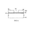
- an opening 60is formed in second insulating layer 58 to provide the structure shown in FIG. 4 .
- Opening 60may be formed by known methods in the art, such as a conventional patterning and etching process. Opening 60 is formed such that the surface of bottom electrode 56 is exposed in opening 60 . After the patterning and etch back process any masking material used is stripped away to leave the structure at a state represented in FIG. 4 .
- a first chalcogenide glasspreferably a germanium-selenide glass layer 62 , is formed in opening 60 on top of bottom electrode 58 .
- the first germanium-selenide glass layer 62is preferably germanium-selenide of Ge x Se 100 ⁇ x stoichiometry. More preferably germanium-selenide glass layer 62 has formula Ge x Se 100 ⁇ x where x is between about 18 and about 33 or about 38 and about 43.
- first germanium-selenide glass layer 62 having the preferred stoichiometric formulamay be accomplished by any appropriate method. Evaporation, co-sputtering germanium and selenium in appropriate ratios, sputtering using a germanium-selenide target having the desired stoichiometry, or chemical vapor deposition with stoichiometric amounts of GeH 4 and SeH 2 gases (or various compositions of these gases), which result in a germanium-selenide layer of the desired stoichiometry are methods which may be used to form germanium-selenide glass layer 62 . First germanium-selenide glass layer 62 is then planarized and etched back by techniques known in the art to provide a structure such as a that shown in FIG. 5 .
- a metalpreferably silver is incorporated into the first germanium-selenide glass layer 62 at step 330 .
- a metalpreferably silver
- the method by which the metal is incorporated into the first germanium-selenide glass layer 62depends on the stoichiometry of the germanium-selenide glass.
- the value of xdetermines the method by which metal is incorporated into the germanium-selenide glass layer.
- metalmay be introduced into first germanium-selenide glass layer 62 by treatment with light irradiation.
- a metal-containing layer 64(preferably containing silver (Ag) or silver-selenide) is deposited over first germanium-selenide glass layer 62 .
- metal and metal-containing layer 64will be further described herein as silver and a silver-containing layer.
- the method of incorporating silver into germanium-selenide glass layer 62varies according to the silver-containing layer 64 utilized. Where silver-containing layer 64 is silver, for example, incorporation of silver into the first germanium-selenide glass layer 62 may be accomplished by irradiating the layers with light. The layers are irradiated for about 5 to 30 minutes at between about 1 mW/cm 2 to about 10 mW/cm 2 with electromagnetic radiation from a wavelength of about 200 nm to about 600 nm.
- the irradiation processbreaks Ge—Se and Se—Se bonds in the first germanium-selenide glass layer 62 , allowing Se from germanium-selenide layer 62 to combine with Ag provided in silver-containing layer 64 and forming silver-selenide first germanium-selenide glass layer 62 .
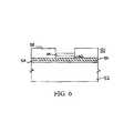
- irradiationmay be used in combination with a thermal process using a temperature of about 50° C. to about 350° C., and preferably about 110° C. for about 5 to about 15 minutes, and more preferably about 10 minutes. This heating drives silver from silver-containing layer 64 into first germanium-selenide glass layer 62 , which may provide an additional source of Ag to bond with Se after the light treatment. Removing excess silver-containing layer 64 from device 50 leaves a first silver-containing germanium-selenide glass layer 68 , as shown in FIG. 7 .
- Other embodiments of the present inventionmay retain silver-containing layer 64 .
- first silver-containing germanium-selenide layer 68may alternatively be obtained by virtue of adjacent placement of germanium-selenide glass layer 62 and silver-containing layer 64 without the irradiation step described above.
- silvermay be introduced to the germanium-selenide glass layer by utilizing a silver-selenide layer as described above.
- a metal-chalcogenide layer 66is deposited on first germanium-selenide glass layer 62 .
- the metal chalcogenideincludes silver-selenide.
- the metal chalcogenide layer 66will be further described herein as a silver-selenide layer.
- Silver-selenide layer 66may be deposited by any suitable method known in the art, with dry plasma deposition (DPD) preferred. Silver-selenide migrates into first germanium-selenide glass layer 62 . Referring to FIG. 7A , this migration of silver into the germanium-selenide glass changes the composition of the first germanium-selenide glass layer to that of a first silver-containing germanium-selenide glass layer 68 . Silver-selenide layer 66 may then be removed by any method known in the art.
- DPDdry plasma deposition
- a second silver-containing germanium-selenide glass layeris subsequently formed in the present invention.
- a second chalcogenide glasspreferably a second germanium-selenide glass layer 70
- This second germanium-selenide glass layer 70preferably has a stoichiometry of Ge x Se 100 ⁇ x .
- the second germanium-selenide glass layer 70preferably has more of an open glass matrix than the first germanium-selenide glass layer 62 , i.e., the second germanium-selenide glass layer preferably contains a smaller proportion of germanium as demonstrated by a smaller value of x.
- One preferred embodimentincludes a first germanium-selenide glass layer 62 having a value of x of about 38 to about 43 (preferably with a value of x of about 40), and a second germanium-selenide glass layer 70 having a value of x of about 18 to about 33 with a value of about 25 preferable.
- This particular embodimentutilizes a first glass with a tight matrix and a second glass with an open matrix as defined by the value of x. It must be understood, however, that both glass can have open matrices and both can have tight matrices.
- a first germanium-selenide glass layer 62may be utilized that has a more open matrix than second germanium-selenide glass layer 70 .
- the present inventionrequires only that there be a diversity in the value of x between the first and second germanium-selenide glass layers 62 , 70 .
- the stoichiometry of second germanium-selenide glass layer 70 and its relative stoichiometry and glass matrix structure with respect to first germanium-selenide glass layer 62is wholly dependent on the desired electrical character of the PCRAM element.
- step 350 of FIG. 2silver is introduced into the second germanium-selenide glass layer 70 .
- Thismay be carried out in accordance with the description of step 330 where silver is introduced into the first germanium-selenide glass layer 62 .
- a second silver-containing layer 72is silver
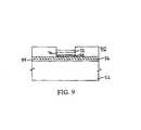
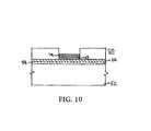
- incorporation of silver into the second germanium-selenide glass layer 70may be accomplished by irradiating the layers with light, as described above. The thermal process described above may also be used with the irradiation process. Removing excess silver-containing layer 72 from device 50 leaves a second silver-containing germanium-selenide glass layer 74 , as shown in FIG. 10 .
- Other embodiments of the present inventionmay retain silver-containing layer 72 .
- second silver-containing germanium-selenide layer 74may alternatively be obtained by virtue of adjacent placement of germanium-selenide glass layer 62 and silver-containing layer 64 without the irradiation step described above.
- xhas a value between about 38 and 43
- a silver-containing layer(preferably comprising silver-selenide) is deposited over second germanium-selenide glass layer 70 , and silver is allowed to migrate from the silver-containing layer to the second germanium-selenide glass layer 70 , as in step 330 .
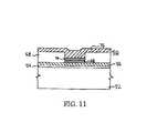
- an upper electrodeis deposited over the previous layer to form a semiconductor device 50 as shown in FIG. 11 .
- the upper electrodeis preferably silver, but may comprise any suitable conductive material.
- the present inventionmay be utilized in any of a number of memory cell configurations known in the art.
- the memory cell 50 A shown in FIG. 11Ais provided where bottom electrode 56 is deposited in an opening formed in first insulating layer 54 , rather than on top of first insulating layer 54 , as shown in FIG. 11 .
- the specific memory cell configurationwill vary according to the specific application of the desired memory cell by altering, among other factors, the deposition and etching processes employed.
- a second embodiment of the present inventionincludes forming at least one additional silver-containing germanium-selenide glass layer above second silver-containing germanium-selenide glass layer 74 .
- a chalcogenide glasspreferably an additional germanium-selenide glass layer 80 , is deposited in opening 60 as shown in FIG. 13 .
- second germanium-selenide glass layer 70is deposited at step 340 .
- the additional germanium-selenide glass layer 80preferably has a stoichiometry of Ge x Se 100 ⁇ x .
- the additional germanium-selenide glass layer 80has a glass matrix structure distinct from any adjacently placed germanium-selenide glass layer, including second silver-containing germanium-selenide glass layer 74 in the case of a first additional silver-containing germanium-selenide glass layer.
- the additional germanium-selenide glass layer 80may have the same glass matrix structure as any germanium-selenide glass layer not adjacent to additional germanium-selenide glass layer 80 , such as first silver-containing germanium-selenide glass layer 68 .
- step 350 B of FIG. 12silver is introduced into the additional germanium-selenide glass layer 80 .
- Thismay be carried out in accordance with the description of step 330 where silver is introduced into the first germanium-selenide glass layer 62 .
- an additional silver-containing layer 82is silver
- incorporation of silver into the additional germanium-selenide glass layer 80may be accomplished by irradiating the layers with light, as described above. The thermal process described above may also be used with the irradiation process. Removing excess silver-containing layer 82 from device 50 leaves an additional silver-containing germanium-selenide glass layer 84 , as shown in FIG. 15 .
- Other embodiments of the present inventionmay retain silver-containing layer 82 .
- additional silver-containing germanium-selenide layer 84may alternatively be obtained by virtue of adjacent placement of additional germanium-selenide glass layer 80 and additional silver-containing layer 82 without the irradiation step described above.
- xhas a value between about 38 and 43
- a silver-containing layer(preferably comprising silver-selenide) is deposited over additional germanium-selenide glass layer 80 , and silver is allowed to migrate from the silver-containing layer to the additional germanium-selenide glass layer 80 , as in step 330 .
- Either method of incorporating silver into the germanium-selenide glass layerresults in an additional silver-containing germanium-selenide glass layer 84 , as shown in FIG. 15 (where silver-containing layer 82 has been stripped).
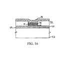
- an upper electrode 76is deposited over the previous layer (in this case 84 ) to form a semiconductor device 50 as shown in FIG. 16 .
- the upper electrodeis preferably silver, but may comprise any suitable conductive material.
- one preferred embodiment of the memory element comprising at least one additional germanium-selenide layerincludes a first silver-containing germanium-selenide glass layer 68 having a value of x of about 38 to about 43 (preferably with a value of x of about 40), and a second silver-containing germanium-selenide glass layer 74 having a value of x of about 18 to about 33 with a value of about 25 preferable.
- the at least one additional silver-containing germanium-selenide layer 84has a value of x different from the value of x for the second silver-containing germanium-selenide glass layer 74 , and preferably from about 38 to about 43, more preferably 40, the same value as x for the first silver-containing germanium-selenide glass layer 68 .
- first silver-containing germanium-selenide glass layer 68 and additional silver-containing germanium-selenide glass layer 84have equal stoichiometries providing a tight glass matrix structure
- second silver-containing germanium-selenide glass layer 74has a stoichiometry providing an open glass matrix structure.
- first and second germanium-selenide glass layers 62 , 70need only have diverse values of x, without a requirement that the first germanium-selenide glass layer 62 have a higher value of x or a tighter glass matrix structure than second germanium-selenide glass layer 70 .
- the present inventionlikewise does not require that additional germanium-selenide glass layer 80 (and consequently additional silver-containing germanium-selenide glass layer 84 ) have any particular value of x or glass matrix structure.
- Additional silver-containing germanium-selenide glass layer 84must only have a value of x and a glass matrix structure different from adjacent silver-containing germanium-selenide glass layers, such as the second silver-containing germanium-selenide glass layer 74 .
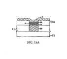
- the memory cell 50 A shown in FIG. 16Ais provided where bottom electrode 56 is deposited in an opening formed in first insulating layer 54 , rather than on top of first insulating layer 54 , as shown in FIG. 16 .
- the specific memory cell configurationwill vary according to the specific application of the desired memory cell by altering, among other factors, the deposition and etching processes employed.
- first and additional silver-containing germanium-selenide glass layers 68 , 84may have equal values of x providing more open glass matrix structure compared to second silver-containing germanium-selenide glass layer 74 having a more tight glass matrix structure.
- first silver-containing germanium-selenide glass layer 68may have a more tight glass matrix structure than second silver-containing germanium-selenide glass layer 74 , which in turn may have a more tight glass matrix structure than additional silver-containing germanium-selenide glass layer 84 , providing a stack of silver-containing germanium-selenide glass layers with descendingly graded stoichiometries. These values of x can be inverted to provide a stack of silver-containing germanium-selenide glass layers with ascendingly graded stoichiometries.
- FIG. 17provides many combinations of silver-containing germanium-selenide stacks for use in memory fabrication.
- a memory element fabricated according to the present inventionalso is not limited in the number of silver-containing germanium-selenide layers included.
- FIG. 17provides four distinct silver-containing germanium-selenide glass layers 68 , 74 , 84 , and 86 .
- Stoichiometries which may be usedare those included in the above description of forming memory elements comprising at least one additional silver-containing germanium-selenide glass layer.
- bottom electrode 56is deposited in an opening formed in first insulating layer 54 , rather than on top of first insulating layer 54 , as shown in FIG. 17 .
- the specific memory cell configurationwill vary according to the specific application of the desired memory cell by altering, among other factors, the deposition and etching processes employed.
- the combination of silver-containing germanium-selenide glass layers 68 , 74 (and 84 , 86 in embodiments comprising at least one additional silver-containing germanium-selenide glass layer)may be selected according to the desired electronic characteristics of the memory element being fabricated. Additionally, utilizing a relatively open-matrix germanium-selenide glass layers with tighter-matrix rigid glass layers provides increased adhesion between the glass and the semiconductor side walls. This is because a more open-matrix glass has greater ability to deform to surface defects and therefore provides greater surface area for contact. The increased presence of free selenium in open-matrix glass may also form bonds with side wall constituents such as silicon, thus aiding in adhesion.
- PCRAM performance with respect to both electrical characteristics and side wall adhesionwill vary depending on the germanium-selenide glass composition, the order of silver-containing germanium-selenide glass layers, and the number of silver-containing germanium-selenide glass layers. It should therefore be readily understood that the invention can be modified in these specific respects as well as to any number of variations, alterations, substitutions or equivalent arrangements not heretofore described, but which are commensurate with the spirit and scope of the invention in order to obtain a desired memory functionality. Accordingly, the invention is not to be seen as limited by the foregoing description, but is only limited by the scope of the appended claims.
Landscapes
- Engineering & Computer Science (AREA)
- Manufacturing & Machinery (AREA)
- Semiconductor Memories (AREA)
Abstract
Description
Claims (25)
Priority Applications (3)
| Application Number | Priority Date | Filing Date | Title |
|---|---|---|---|
| US10/230,327US6856002B2 (en) | 2002-08-29 | 2002-08-29 | Graded GexSe100-x concentration in PCRAM |
| US10/787,121US6953720B2 (en) | 2002-08-29 | 2004-02-27 | Methods for forming chalcogenide glass-based memory elements |
| US11/195,642US7518212B2 (en) | 2002-08-29 | 2005-08-03 | Graded GexSe100-x concentration in PCRAM |
Applications Claiming Priority (1)
| Application Number | Priority Date | Filing Date | Title |
|---|---|---|---|
| US10/230,327US6856002B2 (en) | 2002-08-29 | 2002-08-29 | Graded GexSe100-x concentration in PCRAM |
Related Child Applications (1)
| Application Number | Title | Priority Date | Filing Date |
|---|---|---|---|
| US10/787,121DivisionUS6953720B2 (en) | 2002-08-29 | 2004-02-27 | Methods for forming chalcogenide glass-based memory elements |
Publications (2)
| Publication Number | Publication Date |
|---|---|
| US20040053461A1 US20040053461A1 (en) | 2004-03-18 |
| US6856002B2true US6856002B2 (en) | 2005-02-15 |
Family
ID=31990383
Family Applications (3)
| Application Number | Title | Priority Date | Filing Date |
|---|---|---|---|
| US10/230,327Expired - LifetimeUS6856002B2 (en) | 2002-08-29 | 2002-08-29 | Graded GexSe100-x concentration in PCRAM |
| US10/787,121Expired - LifetimeUS6953720B2 (en) | 2002-08-29 | 2004-02-27 | Methods for forming chalcogenide glass-based memory elements |
| US11/195,642Expired - LifetimeUS7518212B2 (en) | 2002-08-29 | 2005-08-03 | Graded GexSe100-x concentration in PCRAM |
Family Applications After (2)
| Application Number | Title | Priority Date | Filing Date |
|---|---|---|---|
| US10/787,121Expired - LifetimeUS6953720B2 (en) | 2002-08-29 | 2004-02-27 | Methods for forming chalcogenide glass-based memory elements |
| US11/195,642Expired - LifetimeUS7518212B2 (en) | 2002-08-29 | 2005-08-03 | Graded GexSe100-x concentration in PCRAM |
Country Status (1)
| Country | Link |
|---|---|
| US (3) | US6856002B2 (en) |
Cited By (15)
| Publication number | Priority date | Publication date | Assignee | Title |
|---|---|---|---|---|
| US20030082908A1 (en)* | 2001-10-30 | 2003-05-01 | Lowrey Tyler A. | Phase change material memory device |
| US20050266635A1 (en)* | 2002-08-29 | 2005-12-01 | Moore John T | Graded GexSe100-x concentration in PCRAM |
| US20070046572A1 (en)* | 2005-08-26 | 2007-03-01 | Kyoung-Doo Kang | Plasma display panel (PDP) |
| US20070045691A1 (en)* | 2005-08-31 | 2007-03-01 | Samsung Electronics Co., Ltd. | Nano-elastic memory device and method of manufacturing the same |
| US20070097739A1 (en)* | 2005-11-02 | 2007-05-03 | Thomas Happ | Phase change memory cell including multiple phase change material portions |
| US20070215853A1 (en)* | 2003-02-24 | 2007-09-20 | Samsung Electronics Co., Ltd. | Multi-layer phase-changeable memory devices and methods of fabricating the same |
| US20070221905A1 (en)* | 2006-03-17 | 2007-09-27 | Micron Technology, Inc. | Reduced power consumption phase change memory and methods for forming the same |
| US20070267721A1 (en)* | 2006-05-19 | 2007-11-22 | Samsung Electronics Co., Ltd. | Phase Change Memory Cell Employing a GeBiTe Layer as a Phase Change Material Layer, Phase Change Memory Device Including the Same, Electronic System Including the Same and Method of Fabricating the Same |
| US20080121859A1 (en)* | 2006-10-19 | 2008-05-29 | Boise State University | Forced ion migration for chalcogenide phase change memory device |
| US20080169457A1 (en)* | 2003-02-24 | 2008-07-17 | Samsung Electronics Co., Ltd. | Phase changeable memory devices including nitrogen and/or silicon |
| US20100027324A1 (en)* | 2008-08-01 | 2010-02-04 | Boise State University | Variable integrated analog resistor |
| US7825479B2 (en) | 2008-08-06 | 2010-11-02 | International Business Machines Corporation | Electrical antifuse having a multi-thickness dielectric layer |
| US20110079709A1 (en)* | 2009-10-07 | 2011-04-07 | Campbell Kristy A | Wide band sensor |
| US8284590B2 (en) | 2010-05-06 | 2012-10-09 | Boise State University | Integratable programmable capacitive device |
| US8467236B2 (en) | 2008-08-01 | 2013-06-18 | Boise State University | Continuously variable resistor |
Families Citing this family (17)
| Publication number | Priority date | Publication date | Assignee | Title |
|---|---|---|---|---|
| US6881623B2 (en)* | 2001-08-29 | 2005-04-19 | Micron Technology, Inc. | Method of forming chalcogenide comprising devices, method of forming a programmable memory cell of memory circuitry, and a chalcogenide comprising device |
| DE102004025615B4 (en)* | 2004-05-25 | 2008-09-04 | Qimonda Ag | Method for producing a solid electrolyte memory cell |
| US7190048B2 (en)* | 2004-07-19 | 2007-03-13 | Micron Technology, Inc. | Resistance variable memory device and method of fabrication |
| EP1675183A1 (en)* | 2004-12-21 | 2006-06-28 | STMicroelectronics S.r.l. | Phase change memory cell with diode junction selection and manufacturing method thereof |
| KR100650753B1 (en)* | 2005-06-10 | 2006-11-27 | 주식회사 하이닉스반도체 | Phase change memory device and manufacturing method thereof |
| US7825033B2 (en)* | 2006-06-09 | 2010-11-02 | Micron Technology, Inc. | Methods of forming variable resistance memory cells, and methods of etching germanium, antimony, and tellurium-comprising materials |
| KR20080095683A (en)* | 2007-04-25 | 2008-10-29 | 삼성전자주식회사 | Phase change memory device and method of forming the same |
| US8373148B2 (en)* | 2007-04-26 | 2013-02-12 | Spansion Llc | Memory device with improved performance |
| KR100883412B1 (en)* | 2007-05-09 | 2009-02-11 | 삼성전자주식회사 | Method for manufacturing phase change memory device having self-aligned electrode, related device and electronic system |
| KR100881055B1 (en)* | 2007-06-20 | 2009-01-30 | 삼성전자주식회사 | Phase change memory unit, manufacturing method thereof, phase change memory device including same and manufacturing method thereof |
| FR2922368A1 (en)* | 2007-10-16 | 2009-04-17 | Commissariat Energie Atomique | METHOD FOR MANUFACTURING A CBRAM MEMORY HAVING IMPROVED RELIABILITY |
| FR2934711B1 (en)* | 2008-07-29 | 2011-03-11 | Commissariat Energie Atomique | MEMORY DEVICE AND CBRAM MEMORY WITH IMPROVED RELIABILITY. |
| US8624217B2 (en) | 2010-06-25 | 2014-01-07 | International Business Machines Corporation | Planar phase-change memory cell with parallel electrical paths |
| US8575008B2 (en) | 2010-08-31 | 2013-11-05 | International Business Machines Corporation | Post-fabrication self-aligned initialization of integrated devices |
| KR101431656B1 (en)* | 2013-04-05 | 2014-08-21 | 한국과학기술연구원 | Chacogenide switching device using germanium and selenium and manufacture method thereof |
| US9583699B2 (en) | 2015-06-01 | 2017-02-28 | Boise State University | Tunable variable resistance memory device |
| US9583703B2 (en) | 2015-06-01 | 2017-02-28 | Boise State University | Tunable variable resistance memory device |
Citations (109)
| Publication number | Priority date | Publication date | Assignee | Title |
|---|---|---|---|---|
| US3271591A (en) | 1963-09-20 | 1966-09-06 | Energy Conversion Devices Inc | Symmetrical current controlling device |
| US3961314A (en) | 1974-03-05 | 1976-06-01 | Energy Conversion Devices, Inc. | Structure and method for producing an image |
| US3966317A (en) | 1974-04-08 | 1976-06-29 | Energy Conversion Devices, Inc. | Dry process production of archival microform records from hard copy |
| US3983542A (en) | 1970-08-13 | 1976-09-28 | Energy Conversion Devices, Inc. | Method and apparatus for recording information |
| US4177474A (en) | 1977-05-18 | 1979-12-04 | Energy Conversion Devices, Inc. | High temperature amorphous semiconductor member and method of making the same |
| US4267261A (en) | 1971-07-15 | 1981-05-12 | Energy Conversion Devices, Inc. | Method for full format imaging |
| US4368099A (en)* | 1982-02-05 | 1983-01-11 | Rca Corporation | Development of germanium selenide photoresist |
| US4597162A (en) | 1983-01-18 | 1986-07-01 | Energy Conversion Devices, Inc. | Method for making, parallel preprogramming or field programming of electronic matrix arrays |
| US4608296A (en) | 1983-12-06 | 1986-08-26 | Energy Conversion Devices, Inc. | Superconducting films and devices exhibiting AC to DC conversion |
| US4637895A (en) | 1985-04-01 | 1987-01-20 | Energy Conversion Devices, Inc. | Gas mixtures for the vapor deposition of semiconductor material |
| US4646266A (en) | 1984-09-28 | 1987-02-24 | Energy Conversion Devices, Inc. | Programmable semiconductor structures and methods for using the same |
| US4664939A (en) | 1985-04-01 | 1987-05-12 | Energy Conversion Devices, Inc. | Vertical semiconductor processor |
| US4668968A (en) | 1984-05-14 | 1987-05-26 | Energy Conversion Devices, Inc. | Integrated circuit compatible thin film field effect transistor and method of making same |
| US4670763A (en) | 1984-05-14 | 1987-06-02 | Energy Conversion Devices, Inc. | Thin film field effect transistor |
| US4673957A (en) | 1984-05-14 | 1987-06-16 | Energy Conversion Devices, Inc. | Integrated circuit compatible thin film field effect transistor and method of making same |
| US4678679A (en) | 1984-06-25 | 1987-07-07 | Energy Conversion Devices, Inc. | Continuous deposition of activated process gases |
| US4710899A (en) | 1985-06-10 | 1987-12-01 | Energy Conversion Devices, Inc. | Data storage medium incorporating a transition metal for increased switching speed |
| US4728406A (en) | 1986-08-18 | 1988-03-01 | Energy Conversion Devices, Inc. | Method for plasma - coating a semiconductor body |
| US4737379A (en) | 1982-09-24 | 1988-04-12 | Energy Conversion Devices, Inc. | Plasma deposited coatings, and low temperature plasma method of making same |
| US4766471A (en) | 1986-01-23 | 1988-08-23 | Energy Conversion Devices, Inc. | Thin film electro-optical devices |
| US4769338A (en) | 1984-05-14 | 1988-09-06 | Energy Conversion Devices, Inc. | Thin film field effect transistor and method of making same |
| US4775425A (en) | 1987-07-27 | 1988-10-04 | Energy Conversion Devices, Inc. | P and n-type microcrystalline semiconductor alloy material including band gap widening elements, devices utilizing same |
| US4788594A (en) | 1986-10-15 | 1988-11-29 | Energy Conversion Devices, Inc. | Solid state electronic camera including thin film matrix of photosensors |
| US4809044A (en) | 1986-08-22 | 1989-02-28 | Energy Conversion Devices, Inc. | Thin film overvoltage protection devices |
| US4818717A (en) | 1986-06-27 | 1989-04-04 | Energy Conversion Devices, Inc. | Method for making electronic matrix arrays |
| US4843443A (en) | 1984-05-14 | 1989-06-27 | Energy Conversion Devices, Inc. | Thin film field effect transistor and method of making same |
| US4845533A (en) | 1986-08-22 | 1989-07-04 | Energy Conversion Devices, Inc. | Thin film electrical devices with amorphous carbon electrodes and method of making same |
| US4853785A (en) | 1986-10-15 | 1989-08-01 | Energy Conversion Devices, Inc. | Electronic camera including electronic signal storage cartridge |
| US4891330A (en) | 1987-07-27 | 1990-01-02 | Energy Conversion Devices, Inc. | Method of fabricating n-type and p-type microcrystalline semiconductor alloy material including band gap widening elements |
| US5128099A (en) | 1991-02-15 | 1992-07-07 | Energy Conversion Devices, Inc. | Congruent state changeable optical memory material and device |
| US5159661A (en) | 1990-10-05 | 1992-10-27 | Energy Conversion Devices, Inc. | Vertically interconnected parallel distributed processor |
| US5166758A (en) | 1991-01-18 | 1992-11-24 | Energy Conversion Devices, Inc. | Electrically erasable phase change memory |
| US5177567A (en) | 1991-07-19 | 1993-01-05 | Energy Conversion Devices, Inc. | Thin-film structure for chalcogenide electrical switching devices and process therefor |
| US5296716A (en) | 1991-01-18 | 1994-03-22 | Energy Conversion Devices, Inc. | Electrically erasable, directly overwritable, multibit single cell memory elements and arrays fabricated therefrom |
| US5335219A (en) | 1991-01-18 | 1994-08-02 | Ovshinsky Stanford R | Homogeneous composition of microcrystalline semiconductor material, semiconductor devices and directly overwritable memory elements fabricated therefrom, and arrays fabricated from the memory elements |
| US5341328A (en) | 1991-01-18 | 1994-08-23 | Energy Conversion Devices, Inc. | Electrically erasable memory elements having reduced switching current requirements and increased write/erase cycle life |
| US5359205A (en) | 1991-11-07 | 1994-10-25 | Energy Conversion Devices, Inc. | Electrically erasable memory elements characterized by reduced current and improved thermal stability |
| US5406509A (en) | 1991-01-18 | 1995-04-11 | Energy Conversion Devices, Inc. | Electrically erasable, directly overwritable, multibit single cell memory elements and arrays fabricated therefrom |
| US5414271A (en) | 1991-01-18 | 1995-05-09 | Energy Conversion Devices, Inc. | Electrically erasable memory elements having improved set resistance stability |
| US5500532A (en) | 1994-08-18 | 1996-03-19 | Arizona Board Of Regents | Personal electronic dosimeter |
| US5534711A (en) | 1991-01-18 | 1996-07-09 | Energy Conversion Devices, Inc. | Electrically erasable, directly overwritable, multibit single cell memory elements and arrays fabricated therefrom |
| US5534712A (en) | 1991-01-18 | 1996-07-09 | Energy Conversion Devices, Inc. | Electrically erasable memory elements characterized by reduced current and improved thermal stability |
| US5536947A (en) | 1991-01-18 | 1996-07-16 | Energy Conversion Devices, Inc. | Electrically erasable, directly overwritable, multibit single cell memory element and arrays fabricated therefrom |
| US5543737A (en) | 1995-02-10 | 1996-08-06 | Energy Conversion Devices, Inc. | Logical operation circuit employing two-terminal chalcogenide switches |
| US5591501A (en) | 1995-12-20 | 1997-01-07 | Energy Conversion Devices, Inc. | Optical recording medium having a plurality of discrete phase change data recording points |
| US5596522A (en) | 1991-01-18 | 1997-01-21 | Energy Conversion Devices, Inc. | Homogeneous compositions of microcrystalline semiconductor material, semiconductor devices and directly overwritable memory elements fabricated therefrom, and arrays fabricated from the memory elements |
| US5687112A (en) | 1996-04-19 | 1997-11-11 | Energy Conversion Devices, Inc. | Multibit single cell memory element having tapered contact |
| US5694054A (en) | 1995-11-28 | 1997-12-02 | Energy Conversion Devices, Inc. | Integrated drivers for flat panel displays employing chalcogenide logic elements |
| US5714768A (en) | 1995-10-24 | 1998-02-03 | Energy Conversion Devices, Inc. | Second-layer phase change memory array on top of a logic device |
| US5751012A (en) | 1995-06-07 | 1998-05-12 | Micron Technology, Inc. | Polysilicon pillar diode for use in a non-volatile memory cell |
| US5761115A (en) | 1996-05-30 | 1998-06-02 | Axon Technologies Corporation | Programmable metallization cell structure and method of making same |
| US5789277A (en) | 1996-07-22 | 1998-08-04 | Micron Technology, Inc. | Method of making chalogenide memory device |
| US5825046A (en) | 1996-10-28 | 1998-10-20 | Energy Conversion Devices, Inc. | Composite memory material comprising a mixture of phase-change memory material and dielectric material |
| US5912839A (en) | 1998-06-23 | 1999-06-15 | Energy Conversion Devices, Inc. | Universal memory element and method of programming same |
| US5933365A (en) | 1997-06-19 | 1999-08-03 | Energy Conversion Devices, Inc. | Memory element with energy control mechanism |
| WO1999028914A3 (en) | 1997-12-04 | 1999-08-26 | Axon Technologies Corp | Programmable sub-surface aggregating metallization structure and method of making same |
| US6011757A (en) | 1998-01-27 | 2000-01-04 | Ovshinsky; Stanford R. | Optical recording media having increased erasability |
| US6087674A (en) | 1996-10-28 | 2000-07-11 | Energy Conversion Devices, Inc. | Memory element with memory material comprising phase-change material and dielectric material |
| US6141241A (en) | 1998-06-23 | 2000-10-31 | Energy Conversion Devices, Inc. | Universal memory element with systems employing same and apparatus and method for reading, writing and programming same |
| WO2000048196A9 (en) | 1999-02-11 | 2001-11-01 | Univ Arizona | Programmable microelectronic devices and methods of forming and programming same |
| US20020000666A1 (en) | 1998-08-31 | 2002-01-03 | Michael N. Kozicki | Self-repairing interconnections for electrical circuits |
| US6339544B1 (en) | 2000-09-29 | 2002-01-15 | Intel Corporation | Method to enhance performance of thermal resistor device |
| US6348365B1 (en) | 2001-03-02 | 2002-02-19 | Micron Technology, Inc. | PCRAM cell manufacturing |
| WO2002021542A1 (en) | 2000-09-08 | 2002-03-14 | Axon Technologies Corporation | Microelectronic programmable device and methods of forming and programming the same |
| US6404665B1 (en) | 2000-09-29 | 2002-06-11 | Intel Corporation | Compositionally modified resistive electrode |
| US6429064B1 (en) | 2000-09-29 | 2002-08-06 | Intel Corporation | Reduced contact area of sidewall conductor |
| US6437383B1 (en) | 2000-12-21 | 2002-08-20 | Intel Corporation | Dual trench isolation for a phase-change memory cell and method of making same |
| US6462984B1 (en) | 2001-06-29 | 2002-10-08 | Intel Corporation | Biasing scheme of floating unselected wordlines and bitlines of a diode-based memory array |
| US6469364B1 (en) | 1998-08-31 | 2002-10-22 | Arizona Board Of Regents | Programmable interconnection system for electrical circuits |
| US6480438B1 (en) | 2001-06-12 | 2002-11-12 | Ovonyx, Inc. | Providing equal cell programming conditions across a large and high density array of phase-change memory cells |
| US20020168820A1 (en) | 2000-09-08 | 2002-11-14 | Kozicki Michael N. | Microelectronic programmable device and methods of forming and programming the same |
| US6487113B1 (en) | 2001-06-29 | 2002-11-26 | Ovonyx, Inc. | Programming a phase-change memory with slow quench time |
| US6501111B1 (en) | 2000-06-30 | 2002-12-31 | Intel Corporation | Three-dimensional (3D) programmable device |
| US6507061B1 (en) | 2001-08-31 | 2003-01-14 | Intel Corporation | Multiple layer phase-change memory |
| US6511862B2 (en) | 2001-06-30 | 2003-01-28 | Ovonyx, Inc. | Modified contact for programmable devices |
| US6511867B2 (en) | 2001-06-30 | 2003-01-28 | Ovonyx, Inc. | Utilizing atomic layer deposition for programmable device |
| US6512241B1 (en) | 2001-12-31 | 2003-01-28 | Intel Corporation | Phase change material memory device |
| US6514805B2 (en) | 2001-06-30 | 2003-02-04 | Intel Corporation | Trench sidewall profile for device isolation |
| US6531373B2 (en) | 2000-12-27 | 2003-03-11 | Ovonyx, Inc. | Method of forming a phase-change memory cell using silicon on insulator low electrode in charcogenide elements |
| US20030048744A1 (en) | 2001-09-01 | 2003-03-13 | Ovshinsky Stanford R. | Increased data storage in optical data storage and retrieval systems using blue lasers and/or plasmon lenses |
| US20030047765A1 (en)* | 2001-08-30 | 2003-03-13 | Campbell Kristy A. | Stoichiometry for chalcogenide glasses useful for memory devices and method of formation |
| US6534781B2 (en) | 2000-12-26 | 2003-03-18 | Ovonyx, Inc. | Phase-change memory bipolar array utilizing a single shallow trench isolation for creating an individual active area region for two memory array elements and one bipolar base contact |
| US6545287B2 (en) | 2001-09-07 | 2003-04-08 | Intel Corporation | Using selective deposition to form phase-change memory cells |
| US6545907B1 (en) | 2001-10-30 | 2003-04-08 | Ovonyx, Inc. | Technique and apparatus for performing write operations to a phase change material memory device |
| US6555860B2 (en) | 2000-09-29 | 2003-04-29 | Intel Corporation | Compositionally modified resistive electrode |
| US6563164B2 (en) | 2000-09-29 | 2003-05-13 | Ovonyx, Inc. | Compositionally modified resistive electrode |
| US6566700B2 (en) | 2001-10-11 | 2003-05-20 | Ovonyx, Inc. | Carbon-containing interfacial layer for phase-change memory |
| US6567293B1 (en) | 2000-09-29 | 2003-05-20 | Ovonyx, Inc. | Single level metal memory cell using chalcogenide cladding |
| US6569705B2 (en) | 2000-12-21 | 2003-05-27 | Intel Corporation | Metal structure for a phase-change memory device |
| US6570784B2 (en) | 2001-06-29 | 2003-05-27 | Ovonyx, Inc. | Programming a phase-change material memory |
| US6576921B2 (en) | 2001-11-08 | 2003-06-10 | Intel Corporation | Isolating phase change material memory cells |
| US6586761B2 (en) | 2001-09-07 | 2003-07-01 | Intel Corporation | Phase change material memory device |
| US6589714B2 (en) | 2001-06-26 | 2003-07-08 | Ovonyx, Inc. | Method for making programmable resistance memory element using silylated photoresist |
| US6590807B2 (en) | 2001-08-02 | 2003-07-08 | Intel Corporation | Method for reading a structural phase-change memory |
| US6605527B2 (en) | 2001-06-30 | 2003-08-12 | Intel Corporation | Reduced area intersection between electrode and programming element |
| US6613604B2 (en) | 2001-08-02 | 2003-09-02 | Ovonyx, Inc. | Method for making small pore for use in programmable resistance memory element |
| US6625054B2 (en) | 2001-12-28 | 2003-09-23 | Intel Corporation | Method and apparatus to program a phase change memory |
| US6638820B2 (en)* | 2001-02-08 | 2003-10-28 | Micron Technology, Inc. | Method of forming chalcogenide comprising devices, method of precluding diffusion of a metal into adjacent chalcogenide material, and chalcogenide comprising devices |
| US6642102B2 (en) | 2001-06-30 | 2003-11-04 | Intel Corporation | Barrier material encapsulation of programmable material |
| US6646297B2 (en) | 2000-12-26 | 2003-11-11 | Ovonyx, Inc. | Lower electrode isolation in a double-wide trench |
| US20030212724A1 (en) | 2002-05-10 | 2003-11-13 | Ovshinsky Stanford R. | Methods of computing with digital multistate phase change materials |
| US6649928B2 (en) | 2000-12-13 | 2003-11-18 | Intel Corporation | Method to selectively remove one side of a conductive bottom electrode of a phase-change memory cell and structure obtained thereby |
| US6660136B2 (en)* | 2002-03-27 | 2003-12-09 | Micron Technology, Inc. | Method of forming a non-volatile resistance variable device and method of forming a metal layer comprising silver and tungsten |
| US6667900B2 (en) | 2001-12-28 | 2003-12-23 | Ovonyx, Inc. | Method and apparatus to operate a memory cell |
| US6673700B2 (en) | 2001-06-30 | 2004-01-06 | Ovonyx, Inc. | Reduced area intersection between electrode and programming element |
| US6687427B2 (en) | 2000-12-29 | 2004-02-03 | Intel Corporation | Optic switch |
| US6690026B2 (en) | 2001-09-28 | 2004-02-10 | Intel Corporation | Method of fabricating a three-dimensional array of active media |
| US6696355B2 (en) | 2000-12-14 | 2004-02-24 | Ovonyx, Inc. | Method to selectively increase the top resistance of the lower programming electrode in a phase-change memory |
| US20040035401A1 (en) | 2002-08-26 | 2004-02-26 | Subramanian Ramachandran | Hydrogen powered scooter |
Family Cites Families (10)
| Publication number | Priority date | Publication date | Assignee | Title |
|---|---|---|---|---|
| US48744A (en)* | 1865-07-11 | Improved artificial building-block | ||
| US168820A (en)* | 1875-10-11 | Improvement in violins | ||
| US212724A (en)* | 1879-02-25 | Improvement in type-writing machines | ||
| US35401A (en)* | 1862-05-27 | Improvement in buckles | ||
| US666A (en)* | 1838-04-02 | Sfbing-bock for coagh and railroad-gab | ||
| US212725A (en)* | 1879-02-25 | Improvement in spindles for spinning-machines | ||
| GB8409434D0 (en)* | 1984-04-11 | 1984-05-23 | Fordath Ltd | Foundry moulds and cores |
| US6514788B2 (en)* | 2001-05-29 | 2003-02-04 | Bae Systems Information And Electronic Systems Integration Inc. | Method for manufacturing contacts for a Chalcogenide memory device |
| US6574921B2 (en)* | 2001-06-29 | 2003-06-10 | Eric Zimmermann | Closure operator having a handle that rotates as the closure rotates |
| US6856002B2 (en)* | 2002-08-29 | 2005-02-15 | Micron Technology, Inc. | Graded GexSe100-x concentration in PCRAM |
- 2002
- 2002-08-29USUS10/230,327patent/US6856002B2/ennot_activeExpired - Lifetime
- 2004
- 2004-02-27USUS10/787,121patent/US6953720B2/ennot_activeExpired - Lifetime
- 2005
- 2005-08-03USUS11/195,642patent/US7518212B2/ennot_activeExpired - Lifetime
Patent Citations (129)
| Publication number | Priority date | Publication date | Assignee | Title |
|---|---|---|---|---|
| US3271591A (en) | 1963-09-20 | 1966-09-06 | Energy Conversion Devices Inc | Symmetrical current controlling device |
| US3983542A (en) | 1970-08-13 | 1976-09-28 | Energy Conversion Devices, Inc. | Method and apparatus for recording information |
| US3988720A (en) | 1970-08-13 | 1976-10-26 | Energy Conversion Devices, Inc. | Recording and retrieving information in an amorphous memory material using a catalytic material |
| US4267261A (en) | 1971-07-15 | 1981-05-12 | Energy Conversion Devices, Inc. | Method for full format imaging |
| US3961314A (en) | 1974-03-05 | 1976-06-01 | Energy Conversion Devices, Inc. | Structure and method for producing an image |
| US3966317A (en) | 1974-04-08 | 1976-06-29 | Energy Conversion Devices, Inc. | Dry process production of archival microform records from hard copy |
| US4177474A (en) | 1977-05-18 | 1979-12-04 | Energy Conversion Devices, Inc. | High temperature amorphous semiconductor member and method of making the same |
| US4368099A (en)* | 1982-02-05 | 1983-01-11 | Rca Corporation | Development of germanium selenide photoresist |
| US4737379A (en) | 1982-09-24 | 1988-04-12 | Energy Conversion Devices, Inc. | Plasma deposited coatings, and low temperature plasma method of making same |
| US4597162A (en) | 1983-01-18 | 1986-07-01 | Energy Conversion Devices, Inc. | Method for making, parallel preprogramming or field programming of electronic matrix arrays |
| US4608296A (en) | 1983-12-06 | 1986-08-26 | Energy Conversion Devices, Inc. | Superconducting films and devices exhibiting AC to DC conversion |
| US4673957A (en) | 1984-05-14 | 1987-06-16 | Energy Conversion Devices, Inc. | Integrated circuit compatible thin film field effect transistor and method of making same |
| US4668968A (en) | 1984-05-14 | 1987-05-26 | Energy Conversion Devices, Inc. | Integrated circuit compatible thin film field effect transistor and method of making same |
| US4670763A (en) | 1984-05-14 | 1987-06-02 | Energy Conversion Devices, Inc. | Thin film field effect transistor |
| US4843443A (en) | 1984-05-14 | 1989-06-27 | Energy Conversion Devices, Inc. | Thin film field effect transistor and method of making same |
| US4769338A (en) | 1984-05-14 | 1988-09-06 | Energy Conversion Devices, Inc. | Thin film field effect transistor and method of making same |
| US4678679A (en) | 1984-06-25 | 1987-07-07 | Energy Conversion Devices, Inc. | Continuous deposition of activated process gases |
| US4646266A (en) | 1984-09-28 | 1987-02-24 | Energy Conversion Devices, Inc. | Programmable semiconductor structures and methods for using the same |
| US4637895A (en) | 1985-04-01 | 1987-01-20 | Energy Conversion Devices, Inc. | Gas mixtures for the vapor deposition of semiconductor material |
| US4698234A (en) | 1985-04-01 | 1987-10-06 | Energy Conversion Devices, Inc. | Vapor deposition of semiconductor material |
| US4696758A (en) | 1985-04-01 | 1987-09-29 | Energy Conversion Devices, Inc. | Gas mixtures for the vapor deposition of semiconductor material |
| US4664939A (en) | 1985-04-01 | 1987-05-12 | Energy Conversion Devices, Inc. | Vertical semiconductor processor |
| US4710899A (en) | 1985-06-10 | 1987-12-01 | Energy Conversion Devices, Inc. | Data storage medium incorporating a transition metal for increased switching speed |
| US4766471A (en) | 1986-01-23 | 1988-08-23 | Energy Conversion Devices, Inc. | Thin film electro-optical devices |
| US4818717A (en) | 1986-06-27 | 1989-04-04 | Energy Conversion Devices, Inc. | Method for making electronic matrix arrays |
| US4728406A (en) | 1986-08-18 | 1988-03-01 | Energy Conversion Devices, Inc. | Method for plasma - coating a semiconductor body |
| US4809044A (en) | 1986-08-22 | 1989-02-28 | Energy Conversion Devices, Inc. | Thin film overvoltage protection devices |
| US4845533A (en) | 1986-08-22 | 1989-07-04 | Energy Conversion Devices, Inc. | Thin film electrical devices with amorphous carbon electrodes and method of making same |
| US4788594A (en) | 1986-10-15 | 1988-11-29 | Energy Conversion Devices, Inc. | Solid state electronic camera including thin film matrix of photosensors |
| US4853785A (en) | 1986-10-15 | 1989-08-01 | Energy Conversion Devices, Inc. | Electronic camera including electronic signal storage cartridge |
| US4891330A (en) | 1987-07-27 | 1990-01-02 | Energy Conversion Devices, Inc. | Method of fabricating n-type and p-type microcrystalline semiconductor alloy material including band gap widening elements |
| US4775425A (en) | 1987-07-27 | 1988-10-04 | Energy Conversion Devices, Inc. | P and n-type microcrystalline semiconductor alloy material including band gap widening elements, devices utilizing same |
| US5159661A (en) | 1990-10-05 | 1992-10-27 | Energy Conversion Devices, Inc. | Vertically interconnected parallel distributed processor |
| US5406509A (en) | 1991-01-18 | 1995-04-11 | Energy Conversion Devices, Inc. | Electrically erasable, directly overwritable, multibit single cell memory elements and arrays fabricated therefrom |
| US5414271A (en) | 1991-01-18 | 1995-05-09 | Energy Conversion Devices, Inc. | Electrically erasable memory elements having improved set resistance stability |
| US5296716A (en) | 1991-01-18 | 1994-03-22 | Energy Conversion Devices, Inc. | Electrically erasable, directly overwritable, multibit single cell memory elements and arrays fabricated therefrom |
| US5335219A (en) | 1991-01-18 | 1994-08-02 | Ovshinsky Stanford R | Homogeneous composition of microcrystalline semiconductor material, semiconductor devices and directly overwritable memory elements fabricated therefrom, and arrays fabricated from the memory elements |
| US5341328A (en) | 1991-01-18 | 1994-08-23 | Energy Conversion Devices, Inc. | Electrically erasable memory elements having reduced switching current requirements and increased write/erase cycle life |
| US5166758A (en) | 1991-01-18 | 1992-11-24 | Energy Conversion Devices, Inc. | Electrically erasable phase change memory |
| US5596522A (en) | 1991-01-18 | 1997-01-21 | Energy Conversion Devices, Inc. | Homogeneous compositions of microcrystalline semiconductor material, semiconductor devices and directly overwritable memory elements fabricated therefrom, and arrays fabricated from the memory elements |
| US5536947A (en) | 1991-01-18 | 1996-07-16 | Energy Conversion Devices, Inc. | Electrically erasable, directly overwritable, multibit single cell memory element and arrays fabricated therefrom |
| US5534712A (en) | 1991-01-18 | 1996-07-09 | Energy Conversion Devices, Inc. | Electrically erasable memory elements characterized by reduced current and improved thermal stability |
| US5534711A (en) | 1991-01-18 | 1996-07-09 | Energy Conversion Devices, Inc. | Electrically erasable, directly overwritable, multibit single cell memory elements and arrays fabricated therefrom |
| US5128099A (en) | 1991-02-15 | 1992-07-07 | Energy Conversion Devices, Inc. | Congruent state changeable optical memory material and device |
| US5177567A (en) | 1991-07-19 | 1993-01-05 | Energy Conversion Devices, Inc. | Thin-film structure for chalcogenide electrical switching devices and process therefor |
| US5359205A (en) | 1991-11-07 | 1994-10-25 | Energy Conversion Devices, Inc. | Electrically erasable memory elements characterized by reduced current and improved thermal stability |
| US5500532A (en) | 1994-08-18 | 1996-03-19 | Arizona Board Of Regents | Personal electronic dosimeter |
| US5543737A (en) | 1995-02-10 | 1996-08-06 | Energy Conversion Devices, Inc. | Logical operation circuit employing two-terminal chalcogenide switches |
| US5751012A (en) | 1995-06-07 | 1998-05-12 | Micron Technology, Inc. | Polysilicon pillar diode for use in a non-volatile memory cell |
| US5714768A (en) | 1995-10-24 | 1998-02-03 | Energy Conversion Devices, Inc. | Second-layer phase change memory array on top of a logic device |
| US5694054A (en) | 1995-11-28 | 1997-12-02 | Energy Conversion Devices, Inc. | Integrated drivers for flat panel displays employing chalcogenide logic elements |
| US5591501A (en) | 1995-12-20 | 1997-01-07 | Energy Conversion Devices, Inc. | Optical recording medium having a plurality of discrete phase change data recording points |
| US5687112A (en) | 1996-04-19 | 1997-11-11 | Energy Conversion Devices, Inc. | Multibit single cell memory element having tapered contact |
| USRE37259E1 (en) | 1996-04-19 | 2001-07-03 | Energy Conversion Devices, Inc. | Multibit single cell memory element having tapered contact |
| US6084796A (en)* | 1996-05-30 | 2000-07-04 | Axon Technologies Corporation | Programmable metallization cell structure and method of making same |
| US5761115A (en) | 1996-05-30 | 1998-06-02 | Axon Technologies Corporation | Programmable metallization cell structure and method of making same |
| US5896312A (en) | 1996-05-30 | 1999-04-20 | Axon Technologies Corporation | Programmable metallization cell structure and method of making same |
| WO1997048032A8 (en) | 1996-05-30 | 2000-08-10 | Axon Technologies Corp | Programmable metallization cell and method of making |
| US5914893A (en) | 1996-05-30 | 1999-06-22 | Axon Technologies Corporation | Programmable metallization cell structure and method of making same |
| US5789277A (en) | 1996-07-22 | 1998-08-04 | Micron Technology, Inc. | Method of making chalogenide memory device |
| US6087674A (en) | 1996-10-28 | 2000-07-11 | Energy Conversion Devices, Inc. | Memory element with memory material comprising phase-change material and dielectric material |
| US5825046A (en) | 1996-10-28 | 1998-10-20 | Energy Conversion Devices, Inc. | Composite memory material comprising a mixture of phase-change memory material and dielectric material |
| US5933365A (en) | 1997-06-19 | 1999-08-03 | Energy Conversion Devices, Inc. | Memory element with energy control mechanism |
| US6418049B1 (en) | 1997-12-04 | 2002-07-09 | Arizona Board Of Regents | Programmable sub-surface aggregating metallization structure and method of making same |
| WO1999028914A3 (en) | 1997-12-04 | 1999-08-26 | Axon Technologies Corp | Programmable sub-surface aggregating metallization structure and method of making same |
| US6011757A (en) | 1998-01-27 | 2000-01-04 | Ovshinsky; Stanford R. | Optical recording media having increased erasability |
| US5912839A (en) | 1998-06-23 | 1999-06-15 | Energy Conversion Devices, Inc. | Universal memory element and method of programming same |
| US6141241A (en) | 1998-06-23 | 2000-10-31 | Energy Conversion Devices, Inc. | Universal memory element with systems employing same and apparatus and method for reading, writing and programming same |
| US20020000666A1 (en) | 1998-08-31 | 2002-01-03 | Michael N. Kozicki | Self-repairing interconnections for electrical circuits |
| US6469364B1 (en) | 1998-08-31 | 2002-10-22 | Arizona Board Of Regents | Programmable interconnection system for electrical circuits |
| US6388324B2 (en) | 1998-08-31 | 2002-05-14 | Arizona Board Of Regents | Self-repairing interconnections for electrical circuits |
| WO2000048196A9 (en) | 1999-02-11 | 2001-11-01 | Univ Arizona | Programmable microelectronic devices and methods of forming and programming same |
| US6501111B1 (en) | 2000-06-30 | 2002-12-31 | Intel Corporation | Three-dimensional (3D) programmable device |
| WO2002021542A1 (en) | 2000-09-08 | 2002-03-14 | Axon Technologies Corporation | Microelectronic programmable device and methods of forming and programming the same |
| US20020168820A1 (en) | 2000-09-08 | 2002-11-14 | Kozicki Michael N. | Microelectronic programmable device and methods of forming and programming the same |
| US6404665B1 (en) | 2000-09-29 | 2002-06-11 | Intel Corporation | Compositionally modified resistive electrode |
| US6429064B1 (en) | 2000-09-29 | 2002-08-06 | Intel Corporation | Reduced contact area of sidewall conductor |
| US6567293B1 (en) | 2000-09-29 | 2003-05-20 | Ovonyx, Inc. | Single level metal memory cell using chalcogenide cladding |
| US6555860B2 (en) | 2000-09-29 | 2003-04-29 | Intel Corporation | Compositionally modified resistive electrode |
| US6621095B2 (en) | 2000-09-29 | 2003-09-16 | Ovonyx, Inc. | Method to enhance performance of thermal resistor device |
| US6563164B2 (en) | 2000-09-29 | 2003-05-13 | Ovonyx, Inc. | Compositionally modified resistive electrode |
| US6597009B2 (en) | 2000-09-29 | 2003-07-22 | Intel Corporation | Reduced contact area of sidewall conductor |
| US6339544B1 (en) | 2000-09-29 | 2002-01-15 | Intel Corporation | Method to enhance performance of thermal resistor device |
| US6649928B2 (en) | 2000-12-13 | 2003-11-18 | Intel Corporation | Method to selectively remove one side of a conductive bottom electrode of a phase-change memory cell and structure obtained thereby |
| US6696355B2 (en) | 2000-12-14 | 2004-02-24 | Ovonyx, Inc. | Method to selectively increase the top resistance of the lower programming electrode in a phase-change memory |
| US6569705B2 (en) | 2000-12-21 | 2003-05-27 | Intel Corporation | Metal structure for a phase-change memory device |
| US6437383B1 (en) | 2000-12-21 | 2002-08-20 | Intel Corporation | Dual trench isolation for a phase-change memory cell and method of making same |
| US6646297B2 (en) | 2000-12-26 | 2003-11-11 | Ovonyx, Inc. | Lower electrode isolation in a double-wide trench |
| US6593176B2 (en) | 2000-12-26 | 2003-07-15 | Ovonyx, Inc. | Method for forming phase-change memory bipolar array utilizing a single shallow trench isolation for creating an individual active area region for two memory array elements and one bipolar base contact |
| US6534781B2 (en) | 2000-12-26 | 2003-03-18 | Ovonyx, Inc. | Phase-change memory bipolar array utilizing a single shallow trench isolation for creating an individual active area region for two memory array elements and one bipolar base contact |
| US6531373B2 (en) | 2000-12-27 | 2003-03-11 | Ovonyx, Inc. | Method of forming a phase-change memory cell using silicon on insulator low electrode in charcogenide elements |
| US6687427B2 (en) | 2000-12-29 | 2004-02-03 | Intel Corporation | Optic switch |
| US6638820B2 (en)* | 2001-02-08 | 2003-10-28 | Micron Technology, Inc. | Method of forming chalcogenide comprising devices, method of precluding diffusion of a metal into adjacent chalcogenide material, and chalcogenide comprising devices |
| US6348365B1 (en) | 2001-03-02 | 2002-02-19 | Micron Technology, Inc. | PCRAM cell manufacturing |
| US6480438B1 (en) | 2001-06-12 | 2002-11-12 | Ovonyx, Inc. | Providing equal cell programming conditions across a large and high density array of phase-change memory cells |
| US6589714B2 (en) | 2001-06-26 | 2003-07-08 | Ovonyx, Inc. | Method for making programmable resistance memory element using silylated photoresist |
| US6462984B1 (en) | 2001-06-29 | 2002-10-08 | Intel Corporation | Biasing scheme of floating unselected wordlines and bitlines of a diode-based memory array |
| US6487113B1 (en) | 2001-06-29 | 2002-11-26 | Ovonyx, Inc. | Programming a phase-change memory with slow quench time |
| US6687153B2 (en) | 2001-06-29 | 2004-02-03 | Ovonyx, Inc. | Programming a phase-change material memory |
| US6570784B2 (en) | 2001-06-29 | 2003-05-27 | Ovonyx, Inc. | Programming a phase-change material memory |
| US6605527B2 (en) | 2001-06-30 | 2003-08-12 | Intel Corporation | Reduced area intersection between electrode and programming element |
| US6673700B2 (en) | 2001-06-30 | 2004-01-06 | Ovonyx, Inc. | Reduced area intersection between electrode and programming element |
| US6511862B2 (en) | 2001-06-30 | 2003-01-28 | Ovonyx, Inc. | Modified contact for programmable devices |
| US6642102B2 (en) | 2001-06-30 | 2003-11-04 | Intel Corporation | Barrier material encapsulation of programmable material |
| US6511867B2 (en) | 2001-06-30 | 2003-01-28 | Ovonyx, Inc. | Utilizing atomic layer deposition for programmable device |
| US6514805B2 (en) | 2001-06-30 | 2003-02-04 | Intel Corporation | Trench sidewall profile for device isolation |
| US6590807B2 (en) | 2001-08-02 | 2003-07-08 | Intel Corporation | Method for reading a structural phase-change memory |
| US6707712B2 (en) | 2001-08-02 | 2004-03-16 | Intel Corporation | Method for reading a structural phase-change memory |
| US6613604B2 (en) | 2001-08-02 | 2003-09-02 | Ovonyx, Inc. | Method for making small pore for use in programmable resistance memory element |
| US20030047765A1 (en)* | 2001-08-30 | 2003-03-13 | Campbell Kristy A. | Stoichiometry for chalcogenide glasses useful for memory devices and method of formation |
| US6507061B1 (en) | 2001-08-31 | 2003-01-14 | Intel Corporation | Multiple layer phase-change memory |
| US6674115B2 (en) | 2001-08-31 | 2004-01-06 | Intel Corporation | Multiple layer phrase-change memory |
| US20030048744A1 (en) | 2001-09-01 | 2003-03-13 | Ovshinsky Stanford R. | Increased data storage in optical data storage and retrieval systems using blue lasers and/or plasmon lenses |
| US6586761B2 (en) | 2001-09-07 | 2003-07-01 | Intel Corporation | Phase change material memory device |
| US6545287B2 (en) | 2001-09-07 | 2003-04-08 | Intel Corporation | Using selective deposition to form phase-change memory cells |
| US6690026B2 (en) | 2001-09-28 | 2004-02-10 | Intel Corporation | Method of fabricating a three-dimensional array of active media |
| US6566700B2 (en) | 2001-10-11 | 2003-05-20 | Ovonyx, Inc. | Carbon-containing interfacial layer for phase-change memory |
| US6545907B1 (en) | 2001-10-30 | 2003-04-08 | Ovonyx, Inc. | Technique and apparatus for performing write operations to a phase change material memory device |
| US6576921B2 (en) | 2001-11-08 | 2003-06-10 | Intel Corporation | Isolating phase change material memory cells |
| US6673648B2 (en) | 2001-11-08 | 2004-01-06 | Intel Corporation | Isolating phase change material memory cells |
| US6625054B2 (en) | 2001-12-28 | 2003-09-23 | Intel Corporation | Method and apparatus to program a phase change memory |
| US6667900B2 (en) | 2001-12-28 | 2003-12-23 | Ovonyx, Inc. | Method and apparatus to operate a memory cell |
| US6512241B1 (en) | 2001-12-31 | 2003-01-28 | Intel Corporation | Phase change material memory device |
| US6660136B2 (en)* | 2002-03-27 | 2003-12-09 | Micron Technology, Inc. | Method of forming a non-volatile resistance variable device and method of forming a metal layer comprising silver and tungsten |
| US20030212725A1 (en) | 2002-05-10 | 2003-11-13 | Ovshinsky Stanford R. | Methods of factoring and modular arithmetic |
| US6671710B2 (en) | 2002-05-10 | 2003-12-30 | Energy Conversion Devices, Inc. | Methods of computing with digital multistate phase change materials |
| US20030212724A1 (en) | 2002-05-10 | 2003-11-13 | Ovshinsky Stanford R. | Methods of computing with digital multistate phase change materials |
| US6714954B2 (en) | 2002-05-10 | 2004-03-30 | Energy Conversion Devices, Inc. | Methods of factoring and modular arithmetic |
| US20040035401A1 (en) | 2002-08-26 | 2004-02-26 | Subramanian Ramachandran | Hydrogen powered scooter |
Non-Patent Citations (171)
| Title |
|---|
| Abdel-All, A.; Elshafie,A.; Elhawary, M.M., DC electric-field effect in bulk and thin-film Ge5As38Te57 chalcogenide glass, Vacuum 59 (2000) 845-853. |
| Adler, D.; Henisch, H.K.; Mott, S.N., The mechanism of threshold switching in amorphous alloys, Rev. Mod. Phys. 50 (1978) 209-220. |
| Adler, D.; Moss, S.C., Amorphous memories and bistable switches, J. Vac. Sci. Technol. 9 (1972) 1182-1189. |
| Afifi, M.A.; Labib, H.H.; El-Fazary, M.H.; Fadel, M., Electrical and thermal properties of chalcogenide glass system Se75Ge25−xSbx, Appl. Phys. A 55 (1992) 167-169. |
| Afifi, M.A.; Labib, H.H.; El-Fazary, M.H.; Fadel, M., Electrical and thermal properties of chalcogenide glass system Se75Ge25-xSbx, Appl. Phys. A 55 (1992) 167-169. |
| Afifi, M.A.; Labib, H.H.; El-Fazary, M.H.; Fadel,, M., Electrical and thermal properties of chalcogenide glass system Se75Ge25−xSbx, Appl. Phys. A 55 (1972) 335-342. |
| Afifi, M.A.; Labib, H.H.; El-Fazary, M.H.; Fadel,, M., Electrical and thermal properties of chalcogenide glass system Se75Ge25-xSbx, Appl. Phys. A 55 (1972) 335-342. |
| Alekperova, Sh.M.; Gadzhieva, G.S., Current-Voltage characteristics of Ag2Se single crystal near the phase transition, Inorganic Materials 23 (1987) 137-139. |
| Aleksiejunas, A.; Cesnys, A., Switching phenomenon and memory effect in thin-film heterojunction of polycrystalline selenium-silver selenide, Phys. Stat. Sol. (a) 19 (1973) K169-K171. |
| Angell, C.A., Mobile ions in amorphous solids, Annu. Rev. Phys. Chem. 43 (1992) 693-717. |
| Aniya, M., Average electronegativity, medium-range-order, and ionic conductivity in superionic glasses, Solid state Ionics 136-137 (2000) 1085-1989. |
| Asahara, Y.; Izumitani, T., Voltage controlled switching in Cu-As-Se compositions, J. Non-Cryst. Solids 11 (1972) 97-104. |
| Asokan, S.; Prasad, M.V.N.; Parthasarathy, G.; Gopal, E.S.R., Mechanical and chemical thresholds in IV-VI chalcogenide glasses, Phys. Rev. Lett. 62 (1989) 808-810. |
| Baranovskii, S.D.; Cordes, H., On the conduction mechanism in ionic glasses, J. Chem. Phys. 111 (1999) 7546-7557. |
| Belin, R., Taillades, G.; Pradel, A.; Ribes, M., Ion dynamics in superionic chalcogenide glasses: complete conductivity spectra, Solid state Ionics 136-137 (2000) 1025-1029. |
| Belin, R.; Zerouale, A.; Pradel, A.; Ribes, M., Ion dynamics in the argyrodite compound Ag7GeSe5I: non-Arrhenius behavior and complete conductivity spectra, Solid State Ionics 143 (2001) 445-455. |
| Benmore, C.J.; Salmon, P.S., Structure of fast ion conducting and semiconducting glassy chalcogenide alloys, Phys. Rev. Lett. 73 (1994) 264-267. |
| Bernede, J .C., Switching and silver movements in Ag2Se thin films, Phys. Stat. Sol. (a) 57 (1980) K101-K104. |
| Bernede, J.C., Influence du metal des electrodes sur les caracteristiques courant-tension des structures M-Ag2Se-M, Thin solid films 70 (1980) L1-L14. |
| Bernede, J.C., Polarized memory switching in MIS thin films, Thin Solid Films 81 (1981) 155-160. |
| Bernede, J.C.; Abachi, T., Different negative resistance in metal/insulator/metal structures with an upper bilayer electrode, Thin solid films 131 (1985) L61-L64. |
| Bernede, J.C.; Conan, A.; Fousenan't.; El Bouchairi, B.; Goureaux, G., Polarized memory switching effects in Ag2Se/Se/M thin film sandwiches, Thin solid films 97 (1982) 165-171. |
| Bernede, J.C.; Khelil, A.; Kettaf, M.; Conan, A., Transition fromn S- to N-type differential negative resistance in Al—Al203-Ag2−xSe1+x thin film structures, Phys. Stat. Sol. (a) 74 (1982) 217-224. |
| Bernede, J.C.; Khelil, A.; Kettaf, M.; Conan, A., Transition fromn S- to N-type differential negative resistance in Al-Al203-Ag2-xSe1+x thin film structures, Phys. Stat. Sol. (a) 74 (1982) 217-224. |
| Bondarev, V.N.; Pikhitsa, P.V., A dendrite model of current instability in RbAg4I5, Solid State Ionics 70/71 (1994) 72-76. |
| Boolchand, P., Bresser, W.J., Compositional trends in glass transition temperature (Tg), network connectivity and nanoscale chemical phase separation in chalcogenides, Dept. of ECECS, Univ. Cincinnati (Oct. 28, 1999) 45221-0030. |
| Boolchand, P., The maximum in glass transition temperatures (Tg) near x=1/3 in GexSe1−x Glasses, Asian Journal of Physics (2000) 9, 709-72. |
| Boolchand, P., The maximum in glass transition temperatures (Tg) near x=1/3 in GexSe1-x Glasses, Asian Journal of Physics (2000) 9, 709-72. |
| Boolchand, P.; Bresser, W.J., Mobile silver ions and glass formation in solid electrolytes, Nature 410 (2001) 1070-1073. |
| Boolchand, P.; Enzweiler, R.N.; Tenhover, M., Structural ordering of evaporated amorphous chalcogenide alloy films: role of thermal annealing, Diffusion and Defect Data vol. 53-54 (1987) 415-420. |
| Boolchand, P.; Georgiev, D.G.; Goodman, B., Discovery of the Intermediate Phase in Chalcogenide Glasses, J. Optoelectronics and Advanced Materials, 3 (2001), 703. |
| Boolchand, P.; Grothaus, J, Molecular Structure of Melt-Quenched GeSe2 and GeS2 glasses compared, Proc. Int. Conf. Phys. Semicond. (Eds. Chadi and Harrison) 17<th >(1985) 833-36. |
| Boolchand, P.; Grothaus, J, Molecular Structure of Melt-Quenched GeSe2 and GeS2 glasses compared, Proc. Int. Conf. Phys. Semicond. (Eds. Chadi and Harrison) 17th (1985) 833-36. |
| Boolchand, P.; Grothaus, J.; Bresser, W.J.; Suranyi, P., Structural origin of broken chemical order in a GeSe2 glass, Phys. Rev. B 25 (1982) 2975-2978. |
| Boolchand, P.; Grothaus, J.; Phillips, J.C., Broken chemical order and phase separation in GexSe1-x glasses, Solid state comm. 45 (1983) 183-185. |
| Boolchand, P.; Selvanathan, D.; Wang, Y.; Georgiev, D.G.; Bresser, W.J., Onset of Rigidity in steps in chalcogenide glasses, Properties and Applications of Amorphous Materials, M.F. Thorpe and Tichy, L. (eds.) Kluwer Academic Publishers, the Netherlands, 2001, pp. 97-132. |
| Bresser, W.; Boolchand, P.; Suranyi, P., Rigidity percolation and molecular clustering in network glasses, Phys. Rev. Lett. 56 (1986) 2493-2496. |
| Bresser, W.J.; Boolchand, P.; Suranyi, P.; de Neufville, J.P, Intrinsically broken chalcogen chemical order in stoichiometric glasses, Journal de Physique 42 (1981) C4-193-C4-196. |
| Bresser, W.J.; Boolchand, P.; Suranyi, P.; Hernandez, J.G., Molecular phase separation and cluster size in GeSe2 glass, Hyperfine interactions 27 (1986) 389-392. |
| Cahen, D.; Gilet, J.-M.; Schmitz, C.; Chernyak, L.; Gartsman, K.; Jakubowicz, A., Room-Temperature, electric field induced creation of stable devices in CulnSe2 Crystals, Science 258 (1992) 271-274. |
| Chatterjee, R.; Asokan, S.; Titus, S.S.K., Current-controlled negative-resistance behavior and memory switching in bulk As-Te-Se Glasses, J. Phys. D: Appl. Phys. 27 (1994) 2624-2627. |
| Chen, C.H.; Tai, K.L. , Whisker growth induced by Ag photodoping in glassy GexSe1-x films, Appl. Phys. Lett. 37 (1980) 1075-1077. |
| Chen, G.; Cheng, J., Role of nitrogen in the crystallization of silicon nitride-doped chalcogenide glasses, J. Am. Ceram. Soc. 82 (1999) 2934-2936. |
| Chen, G.; Cheng, J.; Chen, W., Effect of Si3N4 on chemical durability of chalcogenide glass, J. Non-Cryst. Solids 220 (1997) 249-253. |
| Cohen, M.H.; Neale, R.G.; Paskin, A., A model for an amorphous semiconductor memory device, J. Non-Cryst. Solids 8-10 (1972) 885-891. |
| Croitoru, N.; Lazarescu, M.; Popescu, C.; Telnic, M.; and Vescan, L., Ohmic and non-ohmic conduction in some amorphous semiconductors, J. Non-Cryst. Solids 8-10 (1972) 781-786. |
| Dalven, R.; Gill, R., Electrical properties of beta-Ag2Te and Beta-Ag2Se from 4.2 to 300K, J. Appl. Phys. 38 (1967) 753-756. |
| Davis, E.A., Semiconductors without form, Search 1 (1970) 152-155. |
| Dearnaley, G.; Stoneham, A.M.; Morgan, D.V., Electrical phenomena in Amorphous oxide films, Rep. Prog. Phys. 33 (1970) 1129-1191. |
| Dejus, R.J.; Susman, S.; Volin, K.J.; Montague, D.G.; Price, D.L., Structure of Vitreous Ag-Ge-Se, J. Non-Cryst. Solids 143 (1992) 162-180. |
| den Boer, W., Threshold switching in hydrogenated amorphous silicon, Appl. Phys. Lett. 40 (1982) 812-813. |
| Drusedau, T.P.; Panckow, A.N.; Klabunde, F., The hydrogenated amorphous silicon/nanodisperse metal (SIMAL) system-Films of unique electronic properties, J. Non-Cryst. Solids 198-200 (1996). 829-832. |
| El Bouchiari, B.; Bernede, J.C.; Burgaud, P., Properties of Ag2−xSe1+x/n-Si Diodes, Thin Solid Films 110 (1983) 107-113. |
| El Bouchiari, B.; Bernede, J.C.; Burgaud, P., Properties of Ag2-xSe1+x/n-Si Diodes, Thin Solid Films 110 (1983) 107-113. |
| El Gharras, Z.; Bourahla, A.; Vautier, C., Role of photoinduced defects in amorphous GexSe1−x photoconductivity, J. Non-Cryst. Solids 155 (1993) 171-179. |
| El Gharras, Z.; Bourahla, A.; Vautier, C., Role of photoinduced defects in amorphous GexSe1-x photoconductivity, J. Non-Cryst. Solids 155 (1993) 171-179. |
| El Ghrandi, R.; Calas, J.; Galibert, G., Ag dissolution kinetics in amorphous GeSe5.5 thin films from "in-situ" resistance measurements vs time, Phys. Stat. Sol. (a) 123 (1991) 451-460. |
| El Ghrandi, R.; Calas, J.; Galibert, G.; Averous, M., Silver photodissolution in amorphous chalcogenide thin films, Thin Solid Films 218 (1992)259-273. |
| El-kady, Y.L., The threshold switching in semiconducting glass Ge21Se17Te62, Indian J. Phys. 70A (1996) 507-516. |
| Elliott, S.R., A unified mechanism for metal photodissolution in amorphous chalcogenide materials, J. Non. Cryst. Solids 130 (1991) 85-97. |
| Elliott, S.R., Photodissolution of metals in chalcogenide glasses: A unified mechanism, J. Non-Cryst. Solids 137-138 (1991) 1031-1034. |
| Elsamanoudy, M.M; Hegab, N.A.; Fadel, M., Conduction mechanism in the pre-switching state of thin films containing Te As Ge Si, Vacuum 46 (1995) 701-707. |
| El-Zahed, H.; El-Korashy, A., Influence of composition on the electrical and optical properties of Ge29BixSe80−x films, Thin Solid Films 376 (2000) 236-240. |
| El-Zahed, H.; El-Korashy, A., Influence of composition on the electrical and optical properties of Ge29BixSe80-x films, Thin Solid Films 376 (2000) 236-240. |
| Fadel, M.; El-Shair, H.T., Electrical, thermal and optical properties of Se75Ge7Sb18, Vacuum 43 (1992) 253-257. |
| Fadel,, M., Switching phenomenon in evaporated Se-Ge-As thin films of amorphous chalcogenide glass, Vacuum 44 (1993) 851-855. |
| Feng, X. ; Bresser, W.J.; Boolchand, P., Direct evidence for stiffness threshold in Chalcogenide glasses, Phys. Rev. Lett. 78 (1997) 4422-4425. |
| Feng, X., Bresser, W.J.; Zhang, M.; Goodman, B.; Boolchand, P., Role of network connectivity on the elastic, plastic and thermal behavior of covalent glasses, J. Non-Cryst. Solids 222 (1997) 137-143. |
| Fischer-Colbrie, A.; Bienenstock, A., Fuoss, P.H.; Marcus, M.A., Structure and bonding in photodiffused amorphous Ag-GeSe2 thin films, Phys. Rev. B 38 (1988) 12388-12403. |
| Fleury, G.; Hamou, A.; Viger, C.; Vautier, C., Conductivity and crystallization of amorphous selenium, Phys. Stat. Sol. (a) 64 (1981) 311-316. |
| Fritzche, H, Optical and electrical energy gaps in amorphous semiconductors, J. Non-Cryst. Solids 6 (1971) 49-71. |
| Fritzsche, H., Electronic phenomena in amorphous semiconductors, Annual Review of Materials Science 2 (1972) 697-744. |
| Gates, B.; Wu, Y.; Yin, Y.; Yang, P.; Xia, Y., Single-crystalline nanowires of Ag2Se can be synthesized by templating against nanowires of trigonal Se, J. Am. Chem. Soc. (2001) currently ASAP. |
| Gosain, D.P.; Nakamura, M.; Shimizu, T.; Suzuki, M.; Okano, S., Nonvolatile memory based on reversible phase transition phenomena in telluride glasses, Jap. J. Appl. Phys. 28 (1989) 1013-1018. |
| Guin, J.-P.; Rouxel, T.; Keryvin, V.; Sangleboeuf, J.-C.; Serre, I.; Lucas, J., Indentation creep of Ge-Se chalcogenide glasses below Tg: elastic recovery and non-Newtonian flow, J. Non-Cryst. Solids 298 (2002) 260-269. |
| Guin, J.-P.; Rouxel, T.; Sangleboeuf, J.-C.; Melscoet, I.; Lucas, J., Hardness, toughness, and scratchability of germanium-selenium chalcogenide glasses, J. Am. Ceram. Soc. 85 (2002) 1545-52. |
| Gupta, Y. P., On electrical switching and memory effects in amorphous chalcogenides, J. Non-Cryst. Sol. 3 (1970) 148-154. |
| Haberland, D.R.; Stiegler, H., New experiments on the charge-controlled switching effect in amorphous semiconductors, J. Non-Cryst. Solids 8-10 (1972) 408-414. |
| Haifz, M.M.; Ibrahim, M.M.; Dongol, M.; Hammad, F.H., Effect of composition on the structure and electrical properties of As-Se-Cu glasses, J. Apply. Phys. 54 (1983) 1950-1954. |
| Hajto, J.; Hu, J.; Snell, A.J.; Turvey, K.; Rose, M., DC and AC measurements on metal/a-Si:H/metal room temperature quantised resistance devices, J. Non-Cryst. Solids 266-269 (2000) 1058-1961. |
| Hajto, J.; McAuley, B.; Snell, A.J.; Owen, A.E., Theory of room temperature quantized resistance effects in metal-a-Si:H-metal thin film stuctures, J. Non-Cryst. Solids 198-200 (1996) 825-828. |
| Hajto, J.; Owen, A.E.; Snell, A.J.; Le Comber, P.G.; Rose, M.J., Analogue memory and ballistic electron effects in metal-amorphous silicon structures, Phil Mag. B 63 (1991) 349-369. |
| Hajto, J.; Rose, M.J.; Osborne, I.S.; Snell, A.J.; LeComber, P.G.; Owen, A.E., Quantization effects in metal/a-Si:H/metal devices, Int. J. Electronics 73 (1992) 911-913. |
| Hayashi, T.; Ono, Y.; Fukaya, M.; Kan, H., Polarized memory switching in amorphous Se film, Japan, J. Appl. Phys. 13 (1974) 1163-1164. |
| Hegab, N.A.; Fadel, M.; Sedeek, K., Memory switching phenomena in thin films of chalcogenide semiconductors, Vacuum 45 (1994) 459-462. |
| Hirose, Y.; Hirose, H., Polarity-dependent memory switching and behavior of Ag dendrite in Ag-photodoped amorphous As2S3 films, J. Appl. Phys. 47 (1976) 2727-2772. |
| Hong, K.S.; Speyer, R.F., Switching behavior in II-IV-V2 amorphous semiconductor systems, J. Non-Cryst. Solids 116 (1990) 191-200. |
| Hosokawa, S., Atomnic and electronic structures of glassy GexSe1−x around the stiffness threshold composition, J. Optoelectronics and Advanced Materials 3 (2001) 199-214. |
| Hosokawa, S., Atomnic and electronic structures of glassy GexSe1-x around the stiffness threshold composition, J. Optoelectronics and Advanced Materials 3 (2001) 199-214. |
| Hu, J.; Hajto, J.; Snell, A.J.; Owen, A.E.; Rose, M.J., Capacitance anomaly near the metal-non-metal transition in Cr-hydrogenated amorphous Si-V thin film devices, Phil. Mag. B 74 (1996) 37-50. |
| Hu, J.; Snell, A.J.; Hajto, J.; Owen, A.E., Constant current forming in Crp+a-/Si:H/V thin film devices, J. Non-Cryst. Solids 227-230 (1998) 1187-1191. |
| Hu, J.; Snell, A.J.; Hajto, J.; Owen, A.E., Current-Induced Instability in Cr-p+a-Si:H-V thin film devices, Phil. Mag. B 80 (2000) 29-43. |
| Iizima, S.; Sugi, M.; Kikuchi, M.; Tanaka, K., Electrical and thermal properties of semiconducting glasses As-Te-Ge, Solid State Comm. 8 (1970) 153-155. |
| Ishikawa, R.; Kikuchi, M., Photovoltaic study on the photo-enhanced diffusion of Ag in amorphous films of Ge2S3, J. Non-Cryst. Solids 35 & 36 (1980) 1061-1066. |
| Iyetomi, H.; Vashishta, P.; Kalia, R.K., Incipient phase separation in Ag/Ge/Se glasses: clustering of Ag atoms, J. Non-Cryst. Solids 262 (2000) 135-142. |
| Jones, G.; Collins, R.A., Switching properties of thin selenium films under pulsed bias, Thin Solid Films 40 (1977) L15-L18. |
| Joullie, A.M.; Marucchi, J., Electrical properties of the amorphous alloy As2Se5, Mat. Res. Bull. 8 (1973) 433-442. |
| Joullie, A.M.; Marucchi, J., On the DC electrical conduction of amorphous As2Se7 before switching, Phys. Stat. Sol. (a) 13 (1972) K105-K109. |
| Kaplan, T.; Adler, D., Electrothermal switching in amorphous semiconductors, J. Non-Cryst. Solids 8-10 (1972) 538-543. |
| Kawaguchi, T.; Maruno, S.; Elliott, S.R., Optical, electrical, and structural properties of amorphous Ag-Ge-S and Ag-Ge-Se films and comparison of photoinduced and thermally induced phenomena of both systems, J. Appl. Phys. 79 (1996) 9096-9104. |
| Kawaguchi, T.; Masui, K., Analysis of change in optical transmission spectra resulting from Ag photodoping in chalcogenide film, Japn. J. Appl. Phys. 26 (1987) 15-21. |
| Kawasaki, M.; Kawamura, J.; Nakamura, Y.; Aniya, M., Ionic conductivity of Agx(GeSe3)1−x (0<=x<=0.571) glasses, Solid state Ionics 123 (1999) 259-269. |
| Kawasaki, M.; Kawamura, J.; Nakamura, Y.; Aniya, M., Ionic conductivity of Agx(GeSe3)1-x (0<=x<=0.571) glasses, Solid state Ionics 123 (1999) 259-269. |
| Kluge, G.; Thomas, A.; Klabes, R.; Grotzschel, R., Silver photodiffusion in amorphous GexSe100−x, J. Non-Cryst. Solids 124 (1990) 186-193. |
| Kluge, G.; Thomas, A.; Klabes, R.; Grotzschel, R., Silver photodiffusion in amorphous GexSe100-x, J. Non-Cryst. Solids 124 (1990) 186-193. |
| Kolobov, A.V., Lateral diffusion of silver in vitreous chalcogenide films, J. Non-Cryst. Solids 137-138 (1991) 1027-1030. |
| Kolobov, A.V., On the origin of p-type conductivity in amorphous chalcogenides, J. Non-Cryst. Solids 198-200 (1996) 728-731. |
| Korkinova, Ts.N.; Andreichin,R.E., Chalcogenide glass polarization and the type of contacts, J. Non-Cryst. Solids 194 (1996) 256-259. |
| Kotkata, M.F.; Afif, M.A.; Labib, H.H.; Hegab, N.A.; Abdel-Aziz, M.M., Memory switching in amorphous GeSeTl chalcogenide semiconductor films, Thin Solid Films 240 (1994) 143-146. |
| Lakshminarayan, K.N.; Srivastava, K.K.; Panwar, O.S.; Dumar, A., Amorphous semiconductor devices: memory and switching mechanism, J. Instn Electronics & Telecom. Engrs 27 (1981) 16-19. |
| Lal, M.; Goyal, N., Chemical bond approach to study the memory and threshold switching chalcogenide glasses, Indian Journal of pure & appl. phys. 29 (1991) 303-304. |
| Leimer, F.; Stotzel, H.; Kottwitz, A., Isothermal electrical polarisation of amorphous GeSe films with blocking Al contacts influenced by Poole-Frenkel conduction, Phys. Stat. Sol. (a) 29 (1975) K129-K132. |
| Leung, W.; Cheung, N.; Neureuther, A.R., Photoinduced diffusion of Ag in GexSe1−x glass, Appl. Phys. Lett. 46 (1985) 543-545. |
| Matsushita, T.; Yamagami, T.; Okuda, M., Polarized memory effect observed on amorphous selenium thin films, Jpn. J. Appl. Phys. 11 (1972) 606. |
| Matsushita, T.; Yamagami, T.; Okuda, M., Polarized memory effect observed on Se—SnO2 system, Jap. J. Appl. Phys. 11 (1972) 1657-1662. |
| Mazurier, F.; Levy, M.; Souquet, J.L, Reversible and irreversible electrical switching in TeO2-V2O5 based glasses, Journal.de.Physique.IV.2 (1992) C2-195-C2-188. |
| Messoussi, R.; Bernede, J.C.; Benhida, S.; Abachi, T.; Latef, A., Electrical characterization of M/Se structures (M=N,Bi), Mat. Chem. And Phys. 28 (1991) 253-258. |
| Mitkova, M.; Boolchand, P., Microscopic origin of the glass forming tendency in chalcogenides and constraint theory, J. Non-Cryst. Solids 240 (1998) 1-21. |
| Mitkova, M.; Kozicki, M.N., Silver incorporation in Ge—Se glasses used in programmable metallization cell devices, J. Non-Cryst. Solids 299-302 (2002) 1023-1027. |
| Mitkova, M.; Wang, Y.; Boolchand, P., Dual chemical role of Ag as an additive in chalcogenide glasses, Phys. Rev. Lett. 83 (1999) 3848-3851. |
| Miyatani, S.-y., Electrical properties of Ag2Se, J. Phys. Soc. Japan 13 (1958) 317. |
| Miyatani, S.-y., Electronic and ionic condition in (AgxCu1−x)2Se, J. Phys. Soc. Japan 34 (1973) 423-432. |
| Miyatani, S.-y., Ionic conduction in beta-Ag2Te and beta-Ag2Se, Journal Phys. Soc. Japan 14 (1959) 996-1002. |
| Mott, N.F., Conduction in glasses containing transition metal ions, J. Non-Cryst. Solids 1 (1968) 1-17. |
| Nakayama, K.; Kitagawa, T.; Ohmura, M.; Suzuki, M., Nonvolatile memory based on phase transitions in chalcogenide thin films, Jpn. J . Appl. Phys. 32 (1993) 564-569. |
| Nakayama, K.; Kojima, K.; Hayakama, F.; Imai, Y.; Kitagawa, A.; Suzuki, M., Submicron nonvolatile memory cell based on reversible phase transition in chalcogenide glasses, Jpn. J. Appl. Phys. 39 (2000) 6157-6161. |
| Nang, T.T.; Okuda, M.; Matsushita, T.; Yokota, S.; Suzuki, A., Electrical and optical parameters of GexSe1−x amorphous thin films, Jap. J. Appl. Phys. 15 (1976) 849-853. |
| Narayanan, R.A.; Asokan, S.; Kumar, A., Evidence concerning the effect of topology on electrical switching in chalcogenide network glasses, Phys. Rev. B 54 (1996) 4413-4415. |
| Neale, R.G.; Aseltine, J.A., The application of amorphous materials to computer memories, IEEE transactions on electron dev. Ed-20 (1973) 195-209. |
| Ovshinsky S.R.; Fritzsche, H., Reversible structural transformations in amorphous semiconductors for memory and logic, Mettalurgical transactions 2 (1971) 641-645. |
| Ovshinsky, S.R., Reversible electrical switching phenomena in disordered structures, Phys. Rev. Lett 21 (1968) 1450-1453. |
| Owen, A.E.; Firth, A.P.; Ewen, P.J.S., Photo-induced structural and physico-chemical changes in amorphous chalcogenide semiconductors, Phil. Mag. B 52 (1985) 347-362. |
| Owen, A.E.; Le Comber, P.G.; Hajto, J.; Rose, M.J.; Snell, A.J., Switching in amorphous devices, Int. J. Electronics 73 (1992) 897-906. |
| Owen, A.E.; LeComber, P.G., Sarrabayrouse, G.; Spear, W.E., New amorphous-silicon electrically programmable nonvolatile switching device, IEE Proc. 129 (1982) 51-54. |
| Pearson, A.D.; Miller, C.E., Filamentary conduction in semiconducting glass diodes, Appl Phys. Lett. 14 (1969) 280-282. |
| Pinto, R.; Ramanathan, K.V., Electric field induced memory switching in thin films of the chalcogenide system Ge—As—Se, Appl. Phys. Lett. 19 (1971) 221-223. |
| Popescu, C., The effect of local non-uniformities on thermal switching and high field behavior of structures with chalcogenide glasses, Solid-state electronics 18 (1975) 671-681. |
| Popescu, C.; Croitoru, N., The contribution of the lateral thermal instability to the switching phenomenon, J. Non-Cryst. Solids 8-10 (1972) 531-537. |
| Popov, A.I., Geller, I.KH.; Shemetova, V.K., Memory and threshold switching effects in amorphous selenium, Phys. Stat. Sol. (a) 44 (1977) K71-K73. |
| Prakash, S.; Asokan, S.; Ghare, D.B., Easily reversible memory switching in Ge—As—Te glasses, J. Phys. D: Appl. Phys. 29 (1996) 2004-2008. |
| Rahman, S.; Sivarama Sastry, G., Electronic switching in Ge—Bi—Se—Te glasses, Mat. Sci. and Eng. B12 (1992) 219-222. |
| Ramesh, K.; Asokan, S.; Sangunni, K.S.; Gopal, E.S.R., Electrical Switching in germanium telluride glasses doped with Cu and Ag, Appl. Phys. A 69 (1999) 421-425. |
| Rose, M.J.;Hajto,J.;Lecomber,P.G.;Gage,S.M.;Choi,W.K.;Snell,A.J.;Owen,A.E., Amorphous silicon analogue memory devices, J. Non-Cryst. Solids 115 (1989) 168-170. |
| Rose, M.J.;Snell,A.J.;Lecomber,P.G.;Hajto,J.;Fitzgerald,A.G.;Owen,A.E., Aspects of non-volatility in a -Si:H memory devices, Mat. Res. Soc. Symp. Proc. V 258, 1992, 1075-1080. |
| Schuocker, D.; Rieder, G., On the reliability of amorphous chalcogenides switching devices, J. Non-Cryst. Solids 29 (1978) 397-407. |
| Sharma, A.L.; Singh, B., Electrical conductivity measurements of evaporated selenium films in vacuum, Proc. Indian Natn. Sci. Acad. 46, A, (1980) 362-368. |
| Sharma., P., Structural, electrical and optical properties of silver selenide films, Inc. J. Of pure and applied phys. 35 (1997) 424-427. |
| Snell, A.J.; Hajto, J.;Rose, M.J.; Osborne, L.S.; Holmes, A.; Owen, A.E.; Gibson, R.A.G., Analogue memory effects in metal/a-Si:H/metal thin film structures, Mat. Res. Soc. Symp. Proc. V 297, 1993, 1017-1021. |
| Snell, A.J.; Lecomber, P.G.; Hajto, J.; Rose, M.J.; Owen, A.E.; Osborne, I.L., Analogue memory effects in metal/a-Si:H/metal memory devices, J. Non-Cryst. Solids 137-138 (1991) 1257-1262. |
| Steventon, A.G., Microfilaments in amorphous chalcogenide memory devices, J. Phys. D: Appl. Phys. 8 (1975) L120-L122. |
| Steventon, A.G., The switching mechanisms in amorphous chalcogenide memory devices, J. Non-Cryst. Solids 21 (1976) 319-329. |
| Stocker, H.J., Bulk and thin film switching and memory effects in semiconducting chalcogenide glasses, App. Phys. Lett. 15 (1969) 55-57. |
| Tanaka, K., Ionic and mixed conductions in Ag photodoping process, Mod. Phys. Lett B 4 (1990) 1373-1377. |
| Tanaka, K.; Iizima, S.; Sugi, M.; Okada, Y.; Kikuchi, M., Thermal effects on switching phenomenon in chalcogenide amorphous semiconductors, Solid State Comm. 8 (1970) 387-389. |
| Thornburg, D.D., Memory switching in a Type I amorphous chalcogenide, J. Elect. Mat. 2 (1973) 3-15. |
| Thornburg, D.D., Memory switching in amorphous arsenic triselenide, J. Non-Cryst. Solids 11 (1972) 113-120. |
| Thornburg, D.D.; White, R.M., Electric field enhanced phase separation and memory switchiong in amorphous arsenic triselenide, Journal(??) (1972) 4609-4612. |
| Tichy, L.; Ticha, H., Remark on the glass-forming ability in GexSe1−x and AsxSe1−x systems, J. Non-Cryst. Solids 261 (2000) 277-281. |
| Titus, S.S.K.; Chatterjee, R.; Asokan, S., Electrical switching and short-range order in As—Te glasses, Phys. Rev. B 48 (1993) 14650-14652. |
| Tranchant,S.;Peytavin,S.;Ribes,M.;Flank,A.M.;Dexpert,H.;Lagarde,J.P., Silver chalcogenide glasses Ag—Ge—Se: Ionic conduction and exafs structural investigation, Transport-structure relations in fast ion and mixed conductors Proceedings of the 6th Riso International symposium. Sep. 9-13, 1985. |
| Tregouet, Y.; Bernede, J.C., Silver movements in Ag2Te thin films: switching and memory effects, Thin Solid Films 57 (1979) 49-54. |
| Uemura, O.; Kameda, Y.; Kokai, S.; Satow, T., Thermally induced crystallization of amorphous Ge0.4Se0.6, J. Non-Cryst. Solids 117-118 (1990) 219-221. |
| Uttecht, R.; Stevenson, H.; Sie, C.H.; Griener, J.D.; Raghavan, K.S., Electric field induced filament formation in As—Te—Ge glass, J. Non-Cryst. Solids 2 (1970) 358-370. |
| Viger, C.; Lefrancois, G.; Fleury, G., Anomalous behavior of amorphous selenium films, J. Non-Cryst. Solids 33 (1976) 267-272. |
| Vodenicharov, C.; Parvanov,S.; Petkov,P., Electrode-limited currents in the thin-film M—GeSe—M system, Mat. Chem. And Phys. 21A (1989) 447-454. |
| Wang, S.-J.; Misium, G.R.; Camp, J.C.; Chen, K.-L.; Tigelaar, H.L., High-performance Metal/silicide antifuse, IEEE electron dev. Lett. 13 (1992)471-472. |
| Weirauch, D.F., Threshold switching and thermal filaments in amorphous semiconductors, App. Phys. Lett. 16 (1970) 72-73. |
| West, W.C., Electrically erasable non-volatile memory via electrochemical deposition of multifractal aggregates, Ph.D. Dissertation, ASU 1998. |
| West, W.C.; Sieradzki, K.; Kardynal, B.; Kozicki, M.N., Equivalent circuit modeling of the Ag|As0.24S0.36Ag0.40|Ag System prepared by photodissolution of Ag, J. Electrochem. Soc. 145 (1998) 2971-2974. |
| Yoji Kawamoto, et al., "Ionic Conduction in As2S3-Ag2S, GeS2-GeS-Ag2S AND P2S5-Ag2S Glasses," Journal of Non-Crystalline Solids 20, pp. 393-404 (1976). |
| Zhang, M.; Mancini, S.; Bresser, W.; Boolchand, P., Variation of glass transition temperature, Tg, with average coordination number, <m>, in network glasses: evidence of a threshold behavior in the slope |dTg/d<m>| at the rigidity percolation threshold (<m>=2.4), J. Non-Cryst. Solids 151 (1992) 149-154. |
Cited By (36)
| Publication number | Priority date | Publication date | Assignee | Title |
|---|---|---|---|---|
| US20030082908A1 (en)* | 2001-10-30 | 2003-05-01 | Lowrey Tyler A. | Phase change material memory device |
| US7319057B2 (en)* | 2001-10-30 | 2008-01-15 | Ovonyx, Inc. | Phase change material memory device |
| US7518212B2 (en)* | 2002-08-29 | 2009-04-14 | Micron Technology, Inc. | Graded GexSe100-x concentration in PCRAM |
| US20050266635A1 (en)* | 2002-08-29 | 2005-12-01 | Moore John T | Graded GexSe100-x concentration in PCRAM |
| US7704787B2 (en) | 2003-02-24 | 2010-04-27 | Samsung Electronics Co., Ltd. | Methods for fabricating phase changeable memory devices |
| US20070215853A1 (en)* | 2003-02-24 | 2007-09-20 | Samsung Electronics Co., Ltd. | Multi-layer phase-changeable memory devices and methods of fabricating the same |
| US7615401B2 (en) | 2003-02-24 | 2009-11-10 | Samsung Electronics Co., Ltd. | Methods of fabricating multi-layer phase-changeable memory devices |
| US20100019216A1 (en)* | 2003-02-24 | 2010-01-28 | Samsung Electronics Co., Ltd. | Multi-layer phase-changeable memory devices |
| US20090004773A1 (en)* | 2003-02-24 | 2009-01-01 | Samsung Electronics Co., Ltd. | Methods of fabricating multi-layer phase-changeable memory devices |
| US20080169457A1 (en)* | 2003-02-24 | 2008-07-17 | Samsung Electronics Co., Ltd. | Phase changeable memory devices including nitrogen and/or silicon |
| US7425735B2 (en) | 2003-02-24 | 2008-09-16 | Samsung Electronics Co., Ltd. | Multi-layer phase-changeable memory devices |
| US7943918B2 (en) | 2003-02-24 | 2011-05-17 | Samsung Electronics Co., Ltd. | Multi-layer phase-changeable memory devices |
| US7462900B2 (en) | 2003-02-24 | 2008-12-09 | Samsung Electronics Co., Ltd. | Phase changeable memory devices including nitrogen and/or silicon |
| US20070046572A1 (en)* | 2005-08-26 | 2007-03-01 | Kyoung-Doo Kang | Plasma display panel (PDP) |
| US7453085B2 (en)* | 2005-08-31 | 2008-11-18 | Samsung Electronics Co., Ltd | Nano-elastic memory device and method of manufacturing the same |
| US20090068782A1 (en)* | 2005-08-31 | 2009-03-12 | Chang Joo-Han | Nano-elastic memory device and method of manufacturing the same |
| US20070045691A1 (en)* | 2005-08-31 | 2007-03-01 | Samsung Electronics Co., Ltd. | Nano-elastic memory device and method of manufacturing the same |
| US7816175B2 (en) | 2005-08-31 | 2010-10-19 | Samsung Electronics Co., Ltd. | Nano-elastic memory device and method of manufacturing the same |
| US20070097739A1 (en)* | 2005-11-02 | 2007-05-03 | Thomas Happ | Phase change memory cell including multiple phase change material portions |
| US7973384B2 (en)* | 2005-11-02 | 2011-07-05 | Qimonda Ag | Phase change memory cell including multiple phase change material portions |
| US20070221905A1 (en)* | 2006-03-17 | 2007-09-27 | Micron Technology, Inc. | Reduced power consumption phase change memory and methods for forming the same |
| US8173988B2 (en) | 2006-03-17 | 2012-05-08 | Micron Technology, Inc. | Reduced power consumption phase change memory and methods for forming the same |
| US7723712B2 (en)* | 2006-03-17 | 2010-05-25 | Micron Technology, Inc. | Reduced power consumption phase change memory and methods for forming the same |
| US20100193759A1 (en)* | 2006-03-17 | 2010-08-05 | Jun Liu | Reduced power consumption phase change memory and methods for forming the same |
| US20070267721A1 (en)* | 2006-05-19 | 2007-11-22 | Samsung Electronics Co., Ltd. | Phase Change Memory Cell Employing a GeBiTe Layer as a Phase Change Material Layer, Phase Change Memory Device Including the Same, Electronic System Including the Same and Method of Fabricating the Same |
| US7817464B2 (en) | 2006-05-19 | 2010-10-19 | Samsung Electronics Co., Ltd. | Phase change memory cell employing a GeBiTe layer as a phase change material layer, phase change memory device including the same, electronic system including the same and method of fabricating the same |
| US20080121859A1 (en)* | 2006-10-19 | 2008-05-29 | Boise State University | Forced ion migration for chalcogenide phase change memory device |
| US7924608B2 (en) | 2006-10-19 | 2011-04-12 | Boise State University | Forced ion migration for chalcogenide phase change memory device |
| US8295081B2 (en) | 2006-10-19 | 2012-10-23 | Boise State University | Forced ion migration for chalcogenide phase change memory device |
| US8611146B2 (en) | 2006-10-19 | 2013-12-17 | Boise State University | Forced ion migration for chalcogenide phase change memory device |
| US20100027324A1 (en)* | 2008-08-01 | 2010-02-04 | Boise State University | Variable integrated analog resistor |
| US8238146B2 (en) | 2008-08-01 | 2012-08-07 | Boise State University | Variable integrated analog resistor |
| US8467236B2 (en) | 2008-08-01 | 2013-06-18 | Boise State University | Continuously variable resistor |
| US7825479B2 (en) | 2008-08-06 | 2010-11-02 | International Business Machines Corporation | Electrical antifuse having a multi-thickness dielectric layer |
| US20110079709A1 (en)* | 2009-10-07 | 2011-04-07 | Campbell Kristy A | Wide band sensor |
| US8284590B2 (en) | 2010-05-06 | 2012-10-09 | Boise State University | Integratable programmable capacitive device |
Also Published As
| Publication number | Publication date |
|---|---|
| US20040185625A1 (en) | 2004-09-23 |
| US6953720B2 (en) | 2005-10-11 |
| US7518212B2 (en) | 2009-04-14 |
| US20040053461A1 (en) | 2004-03-18 |
| US20050266635A1 (en) | 2005-12-01 |
Similar Documents
| Publication | Publication Date | Title |
|---|---|---|
| US6856002B2 (en) | Graded GexSe100-x concentration in PCRAM | |
| US7087919B2 (en) | Layered resistance variable memory device and method of fabrication | |
| US8263958B2 (en) | Layered resistance variable memory device and method of fabrication | |
| US7087454B2 (en) | Fabrication of single polarity programmable resistance structure | |
| EP1483795B1 (en) | Manufacturing methods for resistance variable material cells | |
| US7863597B2 (en) | Resistance variable memory devices with passivating material | |
| US6867114B2 (en) | Methods to form a memory cell with metal-rich metal chalcogenide | |
| US20030143782A1 (en) | Methods of forming germanium selenide comprising devices and methods of forming silver selenide comprising structures | |
| US7374174B2 (en) | Small electrode for resistance variable devices | |
| US7294527B2 (en) | Method of forming a memory cell |
Legal Events
| Date | Code | Title | Description |
|---|---|---|---|
| AS | Assignment | Owner name:MICRON TECHNOLOGY, INC., IDAHO Free format text:ASSIGNMENT OF ASSIGNORS INTEREST;ASSIGNORS:MOORE, JOHN T.;GILTON, TERRY L.;CAMPBELL, KRISTY A.;REEL/FRAME:013244/0170 Effective date:20020829 | |
| STCF | Information on status: patent grant | Free format text:PATENTED CASE | |
| CC | Certificate of correction | ||
| CC | Certificate of correction | ||
| FEPP | Fee payment procedure | Free format text:PAYOR NUMBER ASSIGNED (ORIGINAL EVENT CODE: ASPN); ENTITY STATUS OF PATENT OWNER: LARGE ENTITY | |
| FPAY | Fee payment | Year of fee payment:4 | |
| FPAY | Fee payment | Year of fee payment:8 | |
| AS | Assignment | Owner name:U.S. BANK NATIONAL ASSOCIATION, AS COLLATERAL AGENT, CALIFORNIA Free format text:SECURITY INTEREST;ASSIGNOR:MICRON TECHNOLOGY, INC.;REEL/FRAME:038669/0001 Effective date:20160426 Owner name:U.S. BANK NATIONAL ASSOCIATION, AS COLLATERAL AGEN Free format text:SECURITY INTEREST;ASSIGNOR:MICRON TECHNOLOGY, INC.;REEL/FRAME:038669/0001 Effective date:20160426 | |
| AS | Assignment | Owner name:MORGAN STANLEY SENIOR FUNDING, INC., AS COLLATERAL AGENT, MARYLAND Free format text:PATENT SECURITY AGREEMENT;ASSIGNOR:MICRON TECHNOLOGY, INC.;REEL/FRAME:038954/0001 Effective date:20160426 Owner name:MORGAN STANLEY SENIOR FUNDING, INC., AS COLLATERAL Free format text:PATENT SECURITY AGREEMENT;ASSIGNOR:MICRON TECHNOLOGY, INC.;REEL/FRAME:038954/0001 Effective date:20160426 | |
| FPAY | Fee payment | Year of fee payment:12 | |
| AS | Assignment | Owner name:U.S. BANK NATIONAL ASSOCIATION, AS COLLATERAL AGENT, CALIFORNIA Free format text:CORRECTIVE ASSIGNMENT TO CORRECT THE REPLACE ERRONEOUSLY FILED PATENT #7358718 WITH THE CORRECT PATENT #7358178 PREVIOUSLY RECORDED ON REEL 038669 FRAME 0001. ASSIGNOR(S) HEREBY CONFIRMS THE SECURITY INTEREST;ASSIGNOR:MICRON TECHNOLOGY, INC.;REEL/FRAME:043079/0001 Effective date:20160426 Owner name:U.S. BANK NATIONAL ASSOCIATION, AS COLLATERAL AGEN Free format text:CORRECTIVE ASSIGNMENT TO CORRECT THE REPLACE ERRONEOUSLY FILED PATENT #7358718 WITH THE CORRECT PATENT #7358178 PREVIOUSLY RECORDED ON REEL 038669 FRAME 0001. ASSIGNOR(S) HEREBY CONFIRMS THE SECURITY INTEREST;ASSIGNOR:MICRON TECHNOLOGY, INC.;REEL/FRAME:043079/0001 Effective date:20160426 | |
| AS | Assignment | Owner name:JPMORGAN CHASE BANK, N.A., AS COLLATERAL AGENT, ILLINOIS Free format text:SECURITY INTEREST;ASSIGNORS:MICRON TECHNOLOGY, INC.;MICRON SEMICONDUCTOR PRODUCTS, INC.;REEL/FRAME:047540/0001 Effective date:20180703 Owner name:JPMORGAN CHASE BANK, N.A., AS COLLATERAL AGENT, IL Free format text:SECURITY INTEREST;ASSIGNORS:MICRON TECHNOLOGY, INC.;MICRON SEMICONDUCTOR PRODUCTS, INC.;REEL/FRAME:047540/0001 Effective date:20180703 | |
| AS | Assignment | Owner name:MICRON TECHNOLOGY, INC., IDAHO Free format text:RELEASE BY SECURED PARTY;ASSIGNOR:U.S. BANK NATIONAL ASSOCIATION, AS COLLATERAL AGENT;REEL/FRAME:047243/0001 Effective date:20180629 | |
| AS | Assignment | Owner name:MICRON TECHNOLOGY, INC., IDAHO Free format text:RELEASE BY SECURED PARTY;ASSIGNOR:MORGAN STANLEY SENIOR FUNDING, INC., AS COLLATERAL AGENT;REEL/FRAME:050937/0001 Effective date:20190731 | |
| AS | Assignment | Owner name:MICRON TECHNOLOGY, INC., IDAHO Free format text:RELEASE BY SECURED PARTY;ASSIGNOR:JPMORGAN CHASE BANK, N.A., AS COLLATERAL AGENT;REEL/FRAME:051028/0001 Effective date:20190731 Owner name:MICRON SEMICONDUCTOR PRODUCTS, INC., IDAHO Free format text:RELEASE BY SECURED PARTY;ASSIGNOR:JPMORGAN CHASE BANK, N.A., AS COLLATERAL AGENT;REEL/FRAME:051028/0001 Effective date:20190731 |