US6855989B1 - Damascene finfet gate with selective metal interdiffusion - Google Patents
Damascene finfet gate with selective metal interdiffusionDownload PDFInfo
- Publication number
- US6855989B1 US6855989B1US10/674,520US67452003AUS6855989B1US 6855989 B1US6855989 B1US 6855989B1US 67452003 AUS67452003 AUS 67452003AUS 6855989 B1US6855989 B1US 6855989B1
- Authority
- US
- United States
- Prior art keywords
- layer
- metal material
- gate
- fin
- forming
- Prior art date
- Legal status (The legal status is an assumption and is not a legal conclusion. Google has not performed a legal analysis and makes no representation as to the accuracy of the status listed.)
- Expired - Lifetime
Links
Images


Classifications
- H—ELECTRICITY
- H10—SEMICONDUCTOR DEVICES; ELECTRIC SOLID-STATE DEVICES NOT OTHERWISE PROVIDED FOR
- H10D—INORGANIC ELECTRIC SEMICONDUCTOR DEVICES
- H10D30/00—Field-effect transistors [FET]
- H10D30/01—Manufacture or treatment
- H10D30/021—Manufacture or treatment of FETs having insulated gates [IGFET]
- H10D30/024—Manufacture or treatment of FETs having insulated gates [IGFET] of fin field-effect transistors [FinFET]
- H—ELECTRICITY
- H10—SEMICONDUCTOR DEVICES; ELECTRIC SOLID-STATE DEVICES NOT OTHERWISE PROVIDED FOR
- H10D—INORGANIC ELECTRIC SEMICONDUCTOR DEVICES
- H10D30/00—Field-effect transistors [FET]
- H10D30/60—Insulated-gate field-effect transistors [IGFET]
- H10D30/62—Fin field-effect transistors [FinFET]
- H—ELECTRICITY
- H10—SEMICONDUCTOR DEVICES; ELECTRIC SOLID-STATE DEVICES NOT OTHERWISE PROVIDED FOR
- H10D—INORGANIC ELECTRIC SEMICONDUCTOR DEVICES
- H10D30/00—Field-effect transistors [FET]
- H10D30/60—Insulated-gate field-effect transistors [IGFET]
- H10D30/67—Thin-film transistors [TFT]
- H10D30/6729—Thin-film transistors [TFT] characterised by the electrodes
- H10D30/673—Thin-film transistors [TFT] characterised by the electrodes characterised by the shapes, relative sizes or dispositions of the gate electrodes
- H—ELECTRICITY
- H10—SEMICONDUCTOR DEVICES; ELECTRIC SOLID-STATE DEVICES NOT OTHERWISE PROVIDED FOR
- H10D—INORGANIC ELECTRIC SEMICONDUCTOR DEVICES
- H10D30/00—Field-effect transistors [FET]
- H10D30/60—Insulated-gate field-effect transistors [IGFET]
- H10D30/67—Thin-film transistors [TFT]
- H10D30/6729—Thin-film transistors [TFT] characterised by the electrodes
- H10D30/6737—Thin-film transistors [TFT] characterised by the electrodes characterised by the electrode materials
- H10D30/6739—Conductor-insulator-semiconductor electrodes
Definitions
- the present inventionrelates generally to transistors and, more particularly, to fin field effect transistors (FinFETs).
- FinFETsfin field effect transistors
- MOSFETsplanar metal oxide semiconductor field effect transistors
- problems associated with short channel effectssuch as excessive leakage between the source and drain, become increasingly difficult to overcome.
- mobility degradation and a number of process issuesalso make it difficult to scale conventional MOSFETs to include increasingly smaller device features. New device structures are, therefore, being explored to improve FET performance and allow further device scaling.
- Double-gate MOSFETsrepresent structures that have been considered as candidates for succeeding existing planar MOSFETs.
- double-gate MOSFETstwo gates may be used to control short channel effects.
- a FinFETis a double-gate structure that exhibits good short channel behavior.
- a FinFETincludes a channel formed in a vertical fin.
- the FinFET structuremay be fabricated using layout and process techniques similar to those used for conventional planar MOSFETs.
- Implementations consistent with the present inventionprovide a FinFET that includes a gate having layers of different metal materials.
- a metal material in a first layer of the FinFET gatemay be selected such that it has a different work function than a second metal material in a second layer of the FinFET gate. Due to the diffusivity of the second metal material in the first metal material, after annealing, the second metal material may selectively diffuse through the first metal material.
- the use of different metals for forming adjacent gate layers over a finmay effectively create two FinFET devices with different threshold voltages (V t ).
- the first metal materialmay be associated with a first threshold voltage (V t1 ) and the second metal material may be associated with a second threshold voltage (V t2 ).
- a FinFET device with multiple voltage thresholdspermits the optimization of drive current and/or leakage current for different circuit paths.
- the fin field effect transistorincludes a fin that further includes a channel, a source region formed adjacent a first end of the fin, and a drain region formed adjacent a second end of the fin.
- the fin field effect transistorfurther includes a first layer of metal material that includes a first gate electrode, where the first layer of metal material is formed adjacent the fin.
- the fin field effect transistoralso includes a second layer of metal material formed adjacent the first layer, where the second layer of metal material includes a second gate electrode and where the first layer of metal material includes a different work function than the second layer of metal material.
- the second layer of metal materialis further selectively diffused into the first layer of metal material via metal interdiffusion.
- a method of forming a multiple voltage threshold fin field effect transistorincludes forming a fin and forming a source region adjacent a first end of the fin and a drain region adjacent a second end of the fin.
- the methodfurther includes forming a dummy gate that includes a first material in a first pattern over the fin and forming a dielectric layer adjacent sides of the dummy gate.
- the methodalso includes removing the first material to form a trench in the dielectric layer corresponding to the first pattern and forming a first metal gate layer in the trench, where the first metal gate layer includes a first metal material.
- the methodadditionally includes forming a second metal gate layer in the trench adjacent the first metal gate layer, where the second metal gate layer includes a second metal material and where the second metal material selectively diffuses through the first metal material via metal interdiffusion to produce a multiple voltage threshold finFET.
- FIG. 1illustrates exemplary layers of a silicon-on-insulator (SOI) wafer that may be used for forming a fin of a FinFET consistent with the present invention
- FIG. 2Aillustrates an exemplary fin consistent with the invention
- FIGS. 2B and 2Cillustrate source and drain regions formed adjacent the fin of FIG. 2A consistent with the invention
- FIG. 2Dillustrates a cross-sectional view of the exemplary fin of FIG. 2A consistent with the invention
- FIGS. 3A and 3Billustrate cross-sectional views of dummy oxide and a polysilicon layer formed over the fin of FIG. 2B consistent with the invention
- FIGS. 4A and 4Billustrate the formation of a dummy gate from the polysilicon layer of FIG. 3B consistent with the invention
- FIG. 5illustrates the formation of a dielectric layer adjacent the dummy gate of FIGS. 4A and 4B consistent with the present invention
- FIG. 6illustrates the removal of the dummy gate of FIGS. 4A and 4B to form a gate trench consistent with the present invention
- FIG. 7illustrates formation of gate insulation within the gate trench of FIG. 6 consistent with the present invention
- FIGS. 8A , 8 B and 8 Cillustrate formation of a first metal gate layer within the gate trench of FIG. 7 consistent with the present invention
- FIGS. 9A and 9Billustrate formation of a photoresist layer over the first metal gate layer of FIGS. 8A , 8 B and 8 C consistent with the invention
- FIG. 10illustrates etching of the first metal gate layer of FIGS. 9A and 9B consistent with the invention
- FIGS. 11A , 11 B and 11 Cillustrate formation of a second metal gate layer within the gate trench of FIGS. 8A , 8 B and 8 C consistent with the present invention
- FIG. 12illustrates formation of a crystalline silicon layer consistent with another embodiment of the invention.
- FIG. 13illustrates formation of an oxide layer and an amorphous silicon layer over the crystalline silicon layer of FIG. 12 consistent with the other embodiment of the invention
- FIG. 14illustrates formation of an oxide layer on the amorphous silicon layer of FIG. 13 consistent with the other embodiment of the invention.
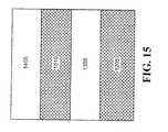
- FIG. 15illustrates formation of a stacked merged FET via metal induced crystallization consistent with the other embodiment of the invention.
- an exemplary damascene process for forming a FinFETis provided.
- a dummy gatemay be formed from a layer of semi-conducting material, such as, for example, polysilicon, that has been formed over a fin.
- a dielectric layermay then be formed over the FinFET fin, source and drain regions around the dummy gate.
- the dummy gatemay then be removed to create a gate trench in the dielectric layer.
- a first layer of a first metal materialmay be formed within the gate trench.
- a second layer of a second metal materialmay be formed within the gate trench adjacent the first layer.
- the first metal material and the second metal materialmay have different work functions such that, after metal interdiffusion of the second metal material into the first metal material, a FinFET device with different threshold voltages (V t ) may be created, with the first metal material being associated with a first threshold voltage (V t1 ) and the second metal material being associated with a second threshold voltage (V t2 ).
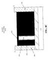
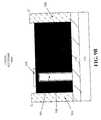
- FIG. 1illustrates a cross-section of a silicon-on-insulator (SOI) wafer 100 formed in accordance with an exemplary embodiment of the present invention.
- SOI wafer 100may include a buried oxide layer 110 formed on a substrate 115 .
- a fin layer 105may further be formed on buried oxide layer 110 .
- the thickness of fin layer 105may range, for example, from about 500 ⁇ to about 2000 ⁇ and the thickness of buried oxide layer 110 may range, for example, from about 1000 ⁇ to about 3000 ⁇ .
- Fin layer 105 and substrate 115may include, for example, silicon, though other semi-conducting materials, such as germanium, may be used.
- a vertical fin 205maybe formed from fin layer 105 .
- Fin 205may be formed, for example, with a width (w) in a range of 10-15 nm. Fin 205 may be formed from fin layer 105 using any conventional process, including, but not limited to, conventional photolithographic and etching processes.
- source 210 and drain 215 regionsmay be formed adjacent respective ends of fin 205 , as shown in FIGS. 2B and 2C .
- Source 210 and drain 215 regionsmay be formed by, for example, deposition of a layer of semi-conducting material over fin 205 .
- the source 210 and drain 215 regionsmay be formed from the layer of semi-conducting material using, for example, conventional photolithographic and etching processes.
- One skilled in the artwill recognize, however, that other existing techniques may be used for forming source 210 and drain 215 regions.
- source 210 and drain 215 regionsmay be formed by patterning and etching fin layer 105 .
- Source 210 and drain 215 regionsmay include a semi-conducting material such as, for example, silicon, germanium or silicon-germanium (Si—Ge). In one implementation, Si x Ge (1-x) , with x approximately equal to 0.7 may be used.
- a cap 220may then be formed on upper surfaces of fin 205 , source 210 and drain 215 , as illustrated in FIG. 2 D.
- Cap 220may include an oxide, such as, for example, silicon oxide, and may range, for example, from about 100 ⁇ to about 500 ⁇ in thickness.
- dummy oxide 305may be formed on fin 205 , source 210 and drain 215 using a conventional process, as shown in FIG. 3 A.
- Dummy oxide 305may be thermally grown on fin 205 , source 210 and drain 215 .
- Dummy oxide 305may include an oxide, such as, for example, silicon oxide and may range, for example, from about 100 ⁇ to about 500 ⁇ in thickness.
- a layer of polysilicon 310may be formed over fin 205 , source 210 and drain 215 .
- the thickness of polysilicon layer 310may range, for example, from about 500 ⁇ to about 2000 ⁇ .
- Polysilicon layer 310may be polished back using, for example, a chemical-mechanical polishing (CMP) process, to achieve a planar surface to improve subsequent gate lithography.
- CMPchemical-mechanical polishing
- a dummy gate 405may be defined in polysilicon layer 310 using a conventional process, such as, for example, a conventional patterning and etching process.
- a dielectric layer 505may be formed over dummy gate 405 using, for example, conventional deposition processes.
- Dielectric layer 505may include, for example, tetraethylorthosilicate (TEOS), or any other dielectric material.
- TEOStetraethylorthosilicate
- the thickness of dielectric layer 505may range, for example, from about 100 ⁇ to about 300 ⁇ .
- Dielectric layer 505may then be polished back to the upper surface of dummy gate 405 using, for example, a CMP process, as illustrated in FIG. 5 .
- Dummy gate 405 and dummy oxide 305may then be removed, as shown in FIG. 6 , leaving a gate trench 605 .
- Dummy gate 405 and dummy oxide 305may be removed using, for example, conventional etching processes.
- Gate insulation 705may then be formed in gate trench 605 , as shown in FIG. 7 .
- Gate insulation 705may be thermally grown or deposited using conventional deposition processes.
- Gate insulation 705may include SiO, SiO 2 , SiN, SiON, HFO 2 , ZrO 2 , Al 2 O 3 , HFSiO(x)ZnS, MgF 2 , or other high-K dielectric materials.
- the thickness of gate insulation layer 705may range, for example, from about 10 ⁇ to about 50 ⁇ .
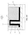
- a first metal material 805may be formed in gate trench 605 over gate insulation 705 .
- Metal material 805may be formed in gate trench 605 using a conventional metal deposition process.
- Metal material 805may include a metal material, such as, for example, Ti or Ni, though other metal materials may alternatively be used.
- the thickness of metal material 805may range, for example, from about 300 ⁇ to about 1000 ⁇ .
- a photoresist pattern 905may be formed over gate material 805 .
- metal material 805may be etched to form a first gate electrode 1005 , as shown in FIG. 10 .
- Photoresist pattern 905may then be removed from first gate electrode 1005 .
- a second metal material 1105may be formed in gate trench 605 over first gate electrode 1005 to form a second gate electrode.
- Metal material 1105may be formed in gate trench 605 using a conventional metal deposition process.
- Metal material 1105may include a metal material, such as, for example, Ni or Ti, though other metal materials may alternatively be used.
- the thickness of metal material 1105may range, for example, from about 300 ⁇ to about 1000 ⁇ .
- Metal material 1105may be selected such that it has a different work function than first metal material 805 .
- second metal material 1105may be selected with a high work function
- first metal material 805may be selected with a low work function. Due to diffusivity of the second metal material 1105 in the first metal material 805 , after annealing, the second metal material 1105 may selectively diffuse through the first metal material to gate insulation 705 .
- the use of different metals for forming adjacent gate electrodes over a finmay effectively create two FinFET devices with different threshold voltages (V t ).
- the first metal material 805may be associated with a first threshold voltage (V t1 ) and the second metal material 1105 may be associated with a second threshold voltage (V t2 ).
- V t1first threshold voltage
- V t2second threshold voltage
- Selective metal interdiffusionthus, achieves different gate work functions for different gate electrodes of a FinFET which, in turn, produces different voltage thresholds (V t ).
- a FinFET device with multiple voltage thresholdspermits the optimization of drive current and/or leakage current for different circuit paths.
- FIGS. 12-15illustrate an exemplary process for forming a stacked merged FET using metal induced crystallization, consistent with another embodiment of the present invention.
- the exemplary processmay begin with the formation of a layer 1205 of amorphous silicon ( ⁇ -Si) material.
- Layer 1205may be formed, for example, using conventional deposition processes and may range, for example, from about 300 ⁇ to about 1000 ⁇ in thickness.
- the amorphous silicon of layer 1205may then be annealed to convert the amorphous silicon to crystalline silicon via metal induced crystallization (MIC).
- MICmetal induced crystallization
- layer 1205may be implanted with an n channel material 1210 to produce an n type FET channel.
- n channel material 1210may include, for example, Si, Ge, or SiGe, and may be implanted to a doping/concentration level that may range, for example, from about 10 15 cm ⁇ 3 to about 10 17 cm ⁇ 3.
- oxide layer 1305may be formed on layer 1205 , as shown in FIG. 13 .
- Oxide layer 1305may include an oxide, such as, for example, silicon oxide and may range, for example, from about 300 ⁇ to about 1000 ⁇ in thickness.
- oxide layer 1305may be thermally grown on layer 1205 .
- a layer 1310 of amorphous silicon ( ⁇ -Si) materialmay then be formed on oxide layer 1305 .
- Layer 1310may be formed, for example, using conventional deposition processes and may range, for example, from about 300 ⁇ to about 1000 ⁇ in thickness.
- layer 1310may be implanted with a p channel material 1315 , such as, for example, Si, Ge, or SiGe, to a doping/concentration level that may range, for example, from about 10 15 cm ⁇ 3 to about 10 17 cm ⁇ 3 .
- a p channel material 1315such as, for example, Si, Ge, or SiGe
- an oxide layer 1405may be formed on layer 1310 .
- Oxide layer 1405may include an oxide, such as, for example, silicon oxide and may range, for example, from about 300 ⁇ to about 1000 ⁇ in thickness.
- oxide layer 1405may be thermally grown on layer 1310 .
- Layers 1205 , 1305 , 1310 and 1405may then be formed into a stack, as shown in FIG. 14 , using a conventional patterning and etching process.
- the amorphous silicon of layer 1310may then be annealed to convert the amorphous silicon to crystalline silicon, via MIC, to produce a p-type crystalline silicon layer 1510 , as illustrated in FIG. 15 .
- Creation of the n-type crystalline silicon layer 1205 and the p-type crystalline silicon layer 1510thus, produces a stacked, merged FET consistent with another embodiment of the invention.
Landscapes
- Electrodes Of Semiconductors (AREA)
- Insulated Gate Type Field-Effect Transistor (AREA)
Abstract
Description
Claims (19)
Priority Applications (1)
| Application Number | Priority Date | Filing Date | Title |
|---|---|---|---|
| US10/674,520US6855989B1 (en) | 2003-10-01 | 2003-10-01 | Damascene finfet gate with selective metal interdiffusion |
Applications Claiming Priority (1)
| Application Number | Priority Date | Filing Date | Title |
|---|---|---|---|
| US10/674,520US6855989B1 (en) | 2003-10-01 | 2003-10-01 | Damascene finfet gate with selective metal interdiffusion |
Publications (1)
| Publication Number | Publication Date |
|---|---|
| US6855989B1true US6855989B1 (en) | 2005-02-15 |
Family
ID=34116818
Family Applications (1)
| Application Number | Title | Priority Date | Filing Date |
|---|---|---|---|
| US10/674,520Expired - LifetimeUS6855989B1 (en) | 2003-10-01 | 2003-10-01 | Damascene finfet gate with selective metal interdiffusion |
Country Status (1)
| Country | Link |
|---|---|
| US (1) | US6855989B1 (en) |
Cited By (22)
| Publication number | Priority date | Publication date | Assignee | Title |
|---|---|---|---|---|
| US20050009311A1 (en)* | 2002-12-09 | 2005-01-13 | John Barnak | Methods of forming a multilayer stack alloy for work function engineering |
| US20050153485A1 (en)* | 2004-01-12 | 2005-07-14 | Ahmed Shibly S. | Narrow-body damascene tri-gate FinFET |
| US6936516B1 (en)* | 2004-01-12 | 2005-08-30 | Advanced Micro Devices, Inc. | Replacement gate strained silicon finFET process |
| US6967175B1 (en) | 2003-12-04 | 2005-11-22 | Advanced Micro Devices, Inc. | Damascene gate semiconductor processing with local thinning of channel region |
| US7026195B2 (en)* | 2004-05-21 | 2006-04-11 | Taiwan Semiconductor Manufacturing Co., Ltd. | Planarizing method for forming FIN-FET device |
| US20060189043A1 (en)* | 2005-02-18 | 2006-08-24 | Thomas Schulz | Trench-gate electrode for FinFET device |
| US20070155118A1 (en)* | 2003-10-17 | 2007-07-05 | Kirklen Henson | Method for forming a notched gate insulator for advanced MIS semiconductor devices and devices thus obtained |
| WO2007093930A1 (en)* | 2006-02-13 | 2007-08-23 | Nxp B.V. | Double-gate semiconductor devices having gates with different work functions and methods of manufacture thereof |
| US20070254435A1 (en)* | 2006-04-27 | 2007-11-01 | Orlowski Marius K | Method for forming a semiconductor device having a fin an structure thereof |
| US20080113476A1 (en)* | 2006-03-28 | 2008-05-15 | International Business Machines Corporation | Dual-plane complementary metal oxide semiconductor |
| US20080230848A1 (en)* | 2007-03-22 | 2008-09-25 | Chih-Chao Yang | Structure having dual silicide region and related method |
| US20100140608A1 (en)* | 2008-12-04 | 2010-06-10 | Samsung Electronics Co., Ltd. | Transistor and method of manufacturing the same |
| US20100163976A1 (en)* | 2008-12-26 | 2010-07-01 | Hynix Semiconductor Inc. | Semiconductor Device Having Saddle Fin Transistor and Method for Fabricating the Same |
| US20100264497A1 (en)* | 2009-04-21 | 2010-10-21 | International Business Machines Corporation | Multiple Vt Field-Effect Transistor Devices |
| US7855105B1 (en) | 2009-06-18 | 2010-12-21 | International Business Machines Corporation | Planar and non-planar CMOS devices with multiple tuned threshold voltages |
| US20130089957A1 (en)* | 2011-03-21 | 2013-04-11 | United Microelectronics Corporation | Fin field-effect transistor structure and manufacturing process thereof |
| CN103165674A (en)* | 2011-12-16 | 2013-06-19 | 台湾积体电路制造股份有限公司 | Finfets with multiple threshold voltages |
| US8803243B2 (en) | 2012-01-03 | 2014-08-12 | International Business Machines Corporation | Complementary metal oxide semiconductor (CMOS) device having gate structures connected by a metal gate conductor |
| US9059217B2 (en) | 2013-03-28 | 2015-06-16 | International Business Machines Corporation | FET semiconductor device with low resistance and enhanced metal fill |
| CN104779148A (en)* | 2014-01-14 | 2015-07-15 | 中芯国际集成电路制造(上海)有限公司 | Semiconductor device manufacturing method |
| US9484270B2 (en) | 2014-09-16 | 2016-11-01 | International Business Machines Corporation | Fully-depleted silicon-on-insulator transistors |
| TWI566280B (en)* | 2015-05-22 | 2017-01-11 | 台灣積體電路製造股份有限公司 | Fin field effect transistor element structure and manufacturing method thereof |
Citations (11)
| Publication number | Priority date | Publication date | Assignee | Title |
|---|---|---|---|---|
| US4319395A (en) | 1979-06-28 | 1982-03-16 | Motorola, Inc. | Method of making self-aligned device |
| US4399605A (en) | 1982-02-26 | 1983-08-23 | International Business Machines Corporation | Method of making dense complementary transistors |
| US20010045589A1 (en) | 2000-05-26 | 2001-11-29 | Fujitsu Limited | Semiconductor device with memory and logic cells |
| US6391750B1 (en) | 1999-08-18 | 2002-05-21 | Advanced Micro Devices, Inc. | Method of selectively controlling contact resistance by controlling impurity concentration and silicide thickness |
| US20020088971A1 (en) | 2000-12-28 | 2002-07-11 | Tsutomu Tezuka | Semiconductor device and method of manufacturing the same |
| US6451693B1 (en) | 2000-10-05 | 2002-09-17 | Advanced Micro Device, Inc. | Double silicide formation in polysicon gate without silicide in source/drain extensions |
| US6589836B1 (en) | 2002-10-03 | 2003-07-08 | Taiwan Semiconductor Manufacturing Company | One step dual salicide formation for ultra shallow junction applications |
| US6657259B2 (en) | 2001-12-04 | 2003-12-02 | International Business Machines Corporation | Multiple-plane FinFET CMOS |
| US20040048424A1 (en) | 2002-09-05 | 2004-03-11 | Taiwan Semiconductor Manufacturing Company | Method of forming an N channel and P channel FINFET device on the same semiconductor substrate |
| US6800905B2 (en)* | 2001-12-14 | 2004-10-05 | International Business Machines Corporation | Implanted asymmetric doped polysilicon gate FinFET |
| US6803631B2 (en)* | 2003-01-23 | 2004-10-12 | Advanced Micro Devices, Inc. | Strained channel finfet |
- 2003
- 2003-10-01USUS10/674,520patent/US6855989B1/ennot_activeExpired - Lifetime
Patent Citations (12)
| Publication number | Priority date | Publication date | Assignee | Title |
|---|---|---|---|---|
| US4319395A (en) | 1979-06-28 | 1982-03-16 | Motorola, Inc. | Method of making self-aligned device |
| US4399605A (en) | 1982-02-26 | 1983-08-23 | International Business Machines Corporation | Method of making dense complementary transistors |
| US6391750B1 (en) | 1999-08-18 | 2002-05-21 | Advanced Micro Devices, Inc. | Method of selectively controlling contact resistance by controlling impurity concentration and silicide thickness |
| US20010045589A1 (en) | 2000-05-26 | 2001-11-29 | Fujitsu Limited | Semiconductor device with memory and logic cells |
| US6451693B1 (en) | 2000-10-05 | 2002-09-17 | Advanced Micro Device, Inc. | Double silicide formation in polysicon gate without silicide in source/drain extensions |
| US20020088971A1 (en) | 2000-12-28 | 2002-07-11 | Tsutomu Tezuka | Semiconductor device and method of manufacturing the same |
| US6657259B2 (en) | 2001-12-04 | 2003-12-02 | International Business Machines Corporation | Multiple-plane FinFET CMOS |
| US20040038464A1 (en) | 2001-12-04 | 2004-02-26 | Fried David M. | Multiple-plane FinFET CMOS |
| US6800905B2 (en)* | 2001-12-14 | 2004-10-05 | International Business Machines Corporation | Implanted asymmetric doped polysilicon gate FinFET |
| US20040048424A1 (en) | 2002-09-05 | 2004-03-11 | Taiwan Semiconductor Manufacturing Company | Method of forming an N channel and P channel FINFET device on the same semiconductor substrate |
| US6589836B1 (en) | 2002-10-03 | 2003-07-08 | Taiwan Semiconductor Manufacturing Company | One step dual salicide formation for ultra shallow junction applications |
| US6803631B2 (en)* | 2003-01-23 | 2004-10-12 | Advanced Micro Devices, Inc. | Strained channel finfet |
Non-Patent Citations (7)
| Title |
|---|
| Co-pending U.S. Appl. No. 10/614,001, filed Jul. 8, 2003, entitled: "Selective Silicidation of Gates in Semiconductor Devices to Achieve Multiple Threshold Voltages"; Shibly S. Ahmed et al.; 20 page specification, 8 sheets of drawings. |
| Copy of co-pending U.S. Appl. No. 10/857,931; by Haihong Wang et al.; filed Jun. 2, 2004; 21 page specification; 20 sheets of drawings. |
| Digh Hisamoto et al.: "FinFET-A Self-Aligned Double-Gate MOSFET Scalable to 20 nm," IEEE Transactions on Electron Devices, vol. 47, No. 12, Dec. 2000, pp. 2320-2325. |
| Xuejue Huang et al.: "Sub 50-nm FinFET: PMOS," 1999 IEEE, IEDM, pp. 67-70. |
| Xuejue Huang et al.: "Sub-50 nm P-Channel Fin FET," IEEE Transactions on Electron Devices, vol. 48, No. 5, May 2001, pp. 880-886. |
| Yang-Kyu Choi et al.: "Nanoscale CMOS Spacer FinFET for the Terabit Era," IEEE Electron Device Letters, vol. 23, No. 1, Jan. 2002, pp. 25-27. |
| Yang-Kyu Choi et al.: "Sub-20nm CMOS Fin FET Technologies," 2001 IEEE, IEDM, pp. 421-424. |
Cited By (54)
| Publication number | Priority date | Publication date | Assignee | Title |
|---|---|---|---|---|
| US20050009311A1 (en)* | 2002-12-09 | 2005-01-13 | John Barnak | Methods of forming a multilayer stack alloy for work function engineering |
| US7122870B2 (en)* | 2002-12-09 | 2006-10-17 | Intel Corporation | Methods of forming a multilayer stack alloy for work function engineering |
| US20070155118A1 (en)* | 2003-10-17 | 2007-07-05 | Kirklen Henson | Method for forming a notched gate insulator for advanced MIS semiconductor devices and devices thus obtained |
| US6967175B1 (en) | 2003-12-04 | 2005-11-22 | Advanced Micro Devices, Inc. | Damascene gate semiconductor processing with local thinning of channel region |
| US20050153485A1 (en)* | 2004-01-12 | 2005-07-14 | Ahmed Shibly S. | Narrow-body damascene tri-gate FinFET |
| US6936516B1 (en)* | 2004-01-12 | 2005-08-30 | Advanced Micro Devices, Inc. | Replacement gate strained silicon finFET process |
| US7186599B2 (en)* | 2004-01-12 | 2007-03-06 | Advanced Micro Devices, Inc. | Narrow-body damascene tri-gate FinFET |
| US7026195B2 (en)* | 2004-05-21 | 2006-04-11 | Taiwan Semiconductor Manufacturing Co., Ltd. | Planarizing method for forming FIN-FET device |
| US20090114979A1 (en)* | 2005-02-18 | 2009-05-07 | Thomas Schulz | FinFET Device with Gate Electrode and Spacers |
| US7679135B2 (en) | 2005-02-18 | 2010-03-16 | Infineon Technologies Ag | FinFET device with gate electrode and spacers |
| US20060189043A1 (en)* | 2005-02-18 | 2006-08-24 | Thomas Schulz | Trench-gate electrode for FinFET device |
| US7488650B2 (en)* | 2005-02-18 | 2009-02-10 | Infineon Technologies Ag | Method of forming trench-gate electrode for FinFET device |
| US7791140B2 (en) | 2006-02-13 | 2010-09-07 | Nxp B.V. | Double-gate semiconductor devices having gates with different work functions and methods of manufacture thereof |
| WO2007093930A1 (en)* | 2006-02-13 | 2007-08-23 | Nxp B.V. | Double-gate semiconductor devices having gates with different work functions and methods of manufacture thereof |
| US20090242987A1 (en)* | 2006-02-13 | 2009-10-01 | Nxp B.V. | Double-gate semiconductor devices having gates with different work functions and methods of manufacture thereof |
| US20080113476A1 (en)* | 2006-03-28 | 2008-05-15 | International Business Machines Corporation | Dual-plane complementary metal oxide semiconductor |
| US7871876B2 (en)* | 2006-03-28 | 2011-01-18 | International Business Machines Corporation | Method of forming a dual-plane complementary metal oxide semiconductor |
| TWI404206B (en)* | 2006-04-27 | 2013-08-01 | Freescale Semiconductor Inc | Method of forming a semiconductor device having fins and structure thereof |
| US7442590B2 (en)* | 2006-04-27 | 2008-10-28 | Freescale Semiconductor, Inc | Method for forming a semiconductor device having a fin and structure thereof |
| US20070254435A1 (en)* | 2006-04-27 | 2007-11-01 | Orlowski Marius K | Method for forming a semiconductor device having a fin an structure thereof |
| CN101432877B (en)* | 2006-04-27 | 2011-09-28 | 飞思卡尔半导体公司 | Method for forming a semiconductor device having a fin and structure thereof |
| US20080230848A1 (en)* | 2007-03-22 | 2008-09-25 | Chih-Chao Yang | Structure having dual silicide region and related method |
| US8373237B2 (en)* | 2008-12-04 | 2013-02-12 | Samsung Electronics Co., Ltd. | Transistor and method of manufacturing the same |
| US20100140608A1 (en)* | 2008-12-04 | 2010-06-10 | Samsung Electronics Co., Ltd. | Transistor and method of manufacturing the same |
| US8815689B2 (en) | 2008-12-26 | 2014-08-26 | SK Hynix Inc. | Method for fabricating a semiconductor device having a saddle fin transistor |
| US20100163976A1 (en)* | 2008-12-26 | 2010-07-01 | Hynix Semiconductor Inc. | Semiconductor Device Having Saddle Fin Transistor and Method for Fabricating the Same |
| US8455945B2 (en) | 2008-12-26 | 2013-06-04 | Hynix Semiconductor Inc. | Semiconductor device having saddle fin transistor and method for fabricating the same |
| US20100264497A1 (en)* | 2009-04-21 | 2010-10-21 | International Business Machines Corporation | Multiple Vt Field-Effect Transistor Devices |
| US8110467B2 (en) | 2009-04-21 | 2012-02-07 | International Business Machines Corporation | Multiple Vt field-effect transistor devices |
| US8878298B2 (en) | 2009-04-21 | 2014-11-04 | International Business Machines Corporation | Multiple Vt field-effect transistor devices |
| US7855105B1 (en) | 2009-06-18 | 2010-12-21 | International Business Machines Corporation | Planar and non-planar CMOS devices with multiple tuned threshold voltages |
| US20100320545A1 (en)* | 2009-06-18 | 2010-12-23 | International Business Machines Corporation | Planar and non-planar cmos devices with multiple tuned threshold voltages |
| US20130089957A1 (en)* | 2011-03-21 | 2013-04-11 | United Microelectronics Corporation | Fin field-effect transistor structure and manufacturing process thereof |
| US8664055B2 (en)* | 2011-03-21 | 2014-03-04 | United Microelectronics Corp. | Fin field-effect transistor structure and manufacturing process thereof |
| US8907431B2 (en)* | 2011-12-16 | 2014-12-09 | Taiwan Semiconductor Manufacturing Company, Ltd. | FinFETs with multiple threshold voltages |
| US9123746B2 (en) | 2011-12-16 | 2015-09-01 | Taiwan Semiconductor Manufacturing Company, Ltd. | FinFETs with multiple threshold voltages |
| US20130154002A1 (en)* | 2011-12-16 | 2013-06-20 | Taiwan Semiconductor Manufacturing Company, Ltd. | FinFETs with Multiple Threshold Voltages |
| CN103165674A (en)* | 2011-12-16 | 2013-06-19 | 台湾积体电路制造股份有限公司 | Finfets with multiple threshold voltages |
| US10020230B2 (en) | 2011-12-16 | 2018-07-10 | Taiwan Semiconductor Manufacturing Company, Ltd. | FinFETs with multiple threshold voltages |
| US9472638B2 (en) | 2011-12-16 | 2016-10-18 | Taiwan Semiconductor Manufacturing Company, Ltd. | FinFETs with multiple threshold voltages |
| CN103165674B (en)* | 2011-12-16 | 2016-08-03 | 台湾积体电路制造股份有限公司 | There is the FinFET of multi-Vt |
| US9082877B2 (en) | 2012-01-03 | 2015-07-14 | International Business Machines Corporation | Complementary metal oxide semiconductor (CMOS) device having gate structures connected by a metal gate conductor |
| US8803243B2 (en) | 2012-01-03 | 2014-08-12 | International Business Machines Corporation | Complementary metal oxide semiconductor (CMOS) device having gate structures connected by a metal gate conductor |
| US9059217B2 (en) | 2013-03-28 | 2015-06-16 | International Business Machines Corporation | FET semiconductor device with low resistance and enhanced metal fill |
| CN104779148A (en)* | 2014-01-14 | 2015-07-15 | 中芯国际集成电路制造(上海)有限公司 | Semiconductor device manufacturing method |
| CN104779148B (en)* | 2014-01-14 | 2019-07-26 | 中芯国际集成电路制造(上海)有限公司 | A method of making a semiconductor device |
| US9484270B2 (en) | 2014-09-16 | 2016-11-01 | International Business Machines Corporation | Fully-depleted silicon-on-insulator transistors |
| US9520329B2 (en) | 2014-09-16 | 2016-12-13 | International Business Machines Corporation | Fully-depleted silicon-on-insulator transistors |
| US9997539B2 (en) | 2014-09-16 | 2018-06-12 | International Business Machines Corporation | Fully-depleted silicon-on-insulator transistors |
| US10163934B2 (en) | 2014-09-16 | 2018-12-25 | International Business Machines Corporation | Fully-depleted silicon-on-insulator transistors |
| US9583485B2 (en) | 2015-05-15 | 2017-02-28 | Taiwan Semiconductor Manufacturing Company, Ltd. | Fin field effect transistor (FinFET) device structure with uneven gate structure and method for forming the same |
| US10468407B2 (en) | 2015-05-15 | 2019-11-05 | Taiwan Semiconductor Manufacturing Co., Ltd. | Fin field effect transistor (FinFET) device structure with uneven gate structure |
| TWI566280B (en)* | 2015-05-22 | 2017-01-11 | 台灣積體電路製造股份有限公司 | Fin field effect transistor element structure and manufacturing method thereof |
| US11139295B2 (en) | 2015-05-22 | 2021-10-05 | Taiwan Semiconductor Manufacturing Co., Ltd. | Fin field effect transistor (FinFET) device and method |
Similar Documents
| Publication | Publication Date | Title |
|---|---|---|
| US6855989B1 (en) | Damascene finfet gate with selective metal interdiffusion | |
| US6686231B1 (en) | Damascene gate process with sacrificial oxide in semiconductor devices | |
| US6872647B1 (en) | Method for forming multiple fins in a semiconductor device | |
| US6645797B1 (en) | Method for forming fins in a FinFET device using sacrificial carbon layer | |
| US6787439B2 (en) | Method using planarizing gate material to improve gate critical dimension in semiconductor devices | |
| US7541267B1 (en) | Reversed T-shaped finfet | |
| US7186599B2 (en) | Narrow-body damascene tri-gate FinFET | |
| US6833588B2 (en) | Semiconductor device having a U-shaped gate structure | |
| US9978870B2 (en) | FinFET with buried insulator layer and method for forming | |
| US6611029B1 (en) | Double gate semiconductor device having separate gates | |
| US6855583B1 (en) | Method for forming tri-gate FinFET with mesa isolation | |
| US6787854B1 (en) | Method for forming a fin in a finFET device | |
| US6709982B1 (en) | Double spacer FinFET formation | |
| US6764884B1 (en) | Method for forming a gate in a FinFET device and thinning a fin in a channel region of the FinFET device | |
| US7084018B1 (en) | Sacrificial oxide for minimizing box undercut in damascene FinFET | |
| US7041542B2 (en) | Damascene tri-gate FinFET | |
| US6876042B1 (en) | Additional gate control for a double-gate MOSFET | |
| US6911697B1 (en) | Semiconductor device having a thin fin and raised source/drain areas | |
| US6936882B1 (en) | Selective silicidation of gates in semiconductor devices to achieve multiple threshold voltages | |
| US6967175B1 (en) | Damascene gate semiconductor processing with local thinning of channel region | |
| US7416925B2 (en) | Doped structure for finfet devices | |
| US7091068B1 (en) | Planarizing sacrificial oxide to improve gate critical dimension in semiconductor devices | |
| US6995438B1 (en) | Semiconductor device with fully silicided source/drain and damascence metal gate |
Legal Events
| Date | Code | Title | Description |
|---|---|---|---|
| AS | Assignment | Owner name:ADVANCED MICRO DEVICES, INC., CALIFORNIA Free format text:ASSIGNMENT OF ASSIGNORS INTEREST;ASSIGNORS:WANG, HAIHONG;AHMED, SHIBLY S.;LIN, MING-REN;AND OTHERS;REEL/FRAME:014565/0198;SIGNING DATES FROM 20030717 TO 20030729 | |
| FEPP | Fee payment procedure | Free format text:PAYOR NUMBER ASSIGNED (ORIGINAL EVENT CODE: ASPN); ENTITY STATUS OF PATENT OWNER: LARGE ENTITY | |
| STCF | Information on status: patent grant | Free format text:PATENTED CASE | |
| FPAY | Fee payment | Year of fee payment:4 | |
| AS | Assignment | Owner name:GLOBALFOUNDRIES INC., CAYMAN ISLANDS Free format text:AFFIRMATION OF PATENT ASSIGNMENT;ASSIGNOR:ADVANCED MICRO DEVICES, INC.;REEL/FRAME:023119/0083 Effective date:20090630 | |
| FPAY | Fee payment | Year of fee payment:8 | |
| FPAY | Fee payment | Year of fee payment:12 | |
| AS | Assignment | Owner name:WILMINGTON TRUST, NATIONAL ASSOCIATION, DELAWARE Free format text:SECURITY AGREEMENT;ASSIGNOR:GLOBALFOUNDRIES INC.;REEL/FRAME:049490/0001 Effective date:20181127 | |
| AS | Assignment | Owner name:GLOBALFOUNDRIES U.S. INC., CALIFORNIA Free format text:ASSIGNMENT OF ASSIGNORS INTEREST;ASSIGNOR:GLOBALFOUNDRIES INC.;REEL/FRAME:054633/0001 Effective date:20201022 | |
| AS | Assignment | Owner name:GLOBALFOUNDRIES INC., CAYMAN ISLANDS Free format text:RELEASE BY SECURED PARTY;ASSIGNOR:WILMINGTON TRUST, NATIONAL ASSOCIATION;REEL/FRAME:054636/0001 Effective date:20201117 | |
| AS | Assignment | Owner name:GLOBALFOUNDRIES U.S. INC., NEW YORK Free format text:RELEASE BY SECURED PARTY;ASSIGNOR:WILMINGTON TRUST, NATIONAL ASSOCIATION;REEL/FRAME:056987/0001 Effective date:20201117 |