US6855980B2 - Semiconductor memory array of floating gate memory cells with low resistance source regions and high source coupling - Google Patents
Semiconductor memory array of floating gate memory cells with low resistance source regions and high source couplingDownload PDFInfo
- Publication number
- US6855980B2 US6855980B2US10/690,204US69020403AUS6855980B2US 6855980 B2US6855980 B2US 6855980B2US 69020403 AUS69020403 AUS 69020403AUS 6855980 B2US6855980 B2US 6855980B2
- Authority
- US
- United States
- Prior art keywords
- layer
- regions
- region
- over
- floating gate
- Prior art date
- Legal status (The legal status is an assumption and is not a legal conclusion. Google has not performed a legal analysis and makes no representation as to the accuracy of the status listed.)
- Expired - Lifetime
Links
- 238000007667floatingMethods0.000titleclaimsabstractdescription67
- 239000004065semiconductorSubstances0.000titleclaimsabstractdescription22
- 230000008878couplingEffects0.000titledescription13
- 238000010168coupling processMethods0.000titledescription13
- 238000005859coupling reactionMethods0.000titledescription13
- 239000000758substrateSubstances0.000claimsabstractdescription72
- 238000002955isolationMethods0.000claimsabstractdescription27
- 239000000463materialSubstances0.000claimsdescription21
- 239000012774insulation materialSubstances0.000claimsdescription17
- 230000005689Fowler Nordheim tunnelingEffects0.000claims2
- 238000000034methodMethods0.000abstractdescription83
- 239000004020conductorSubstances0.000abstractdescription39
- 238000007373indentationMethods0.000abstractdescription6
- 239000010410layerSubstances0.000description256
- 150000004767nitridesChemical class0.000description78
- 125000006850spacer groupChemical group0.000description38
- VYPSYNLAJGMNEJ-UHFFFAOYSA-NSilicium dioxideChemical compoundO=[Si]=OVYPSYNLAJGMNEJ-UHFFFAOYSA-N0.000description37
- XUIMIQQOPSSXEZ-UHFFFAOYSA-NSiliconChemical compound[Si]XUIMIQQOPSSXEZ-UHFFFAOYSA-N0.000description35
- 229910052751metalInorganic materials0.000description34
- 239000002184metalSubstances0.000description34
- 230000015572biosynthetic processEffects0.000description27
- 229910021420polycrystalline siliconInorganic materials0.000description26
- 229920005591polysiliconPolymers0.000description26
- 238000000151depositionMethods0.000description24
- 238000009413insulationMethods0.000description24
- 229910052710siliconInorganic materials0.000description22
- 239000010703siliconSubstances0.000description22
- HQVNEWCFYHHQES-UHFFFAOYSA-Nsilicon nitrideChemical compoundN12[Si]34N5[Si]62N3[Si]51N64HQVNEWCFYHHQES-UHFFFAOYSA-N0.000description19
- 229910021332silicideInorganic materials0.000description18
- FVBUAEGBCNSCDD-UHFFFAOYSA-Nsilicide(4-)Chemical compound[Si-4]FVBUAEGBCNSCDD-UHFFFAOYSA-N0.000description18
- 230000000873masking effectEffects0.000description17
- 239000005380borophosphosilicate glassSubstances0.000description16
- PXHVJJICTQNCMI-UHFFFAOYSA-NNickelChemical compound[Ni]PXHVJJICTQNCMI-UHFFFAOYSA-N0.000description12
- BASFCYQUMIYNBI-UHFFFAOYSA-NplatinumChemical compound[Pt]BASFCYQUMIYNBI-UHFFFAOYSA-N0.000description12
- 229910052581Si3N4Inorganic materials0.000description11
- WFKWXMTUELFFGS-UHFFFAOYSA-NtungstenChemical compound[W]WFKWXMTUELFFGS-UHFFFAOYSA-N0.000description11
- 229910052721tungstenInorganic materials0.000description11
- 239000010937tungstenSubstances0.000description11
- 230000008021depositionEffects0.000description10
- 229960001866silicon dioxideDrugs0.000description9
- 235000012239silicon dioxideNutrition0.000description9
- 239000000377silicon dioxideSubstances0.000description9
- 238000005530etchingMethods0.000description8
- 238000005229chemical vapour depositionMethods0.000description7
- ZOKXTWBITQBERF-UHFFFAOYSA-NMolybdenumChemical compound[Mo]ZOKXTWBITQBERF-UHFFFAOYSA-N0.000description6
- RTAQQCXQSZGOHL-UHFFFAOYSA-NTitaniumChemical compound[Ti]RTAQQCXQSZGOHL-UHFFFAOYSA-N0.000description6
- NRTOMJZYCJJWKI-UHFFFAOYSA-NTitanium nitrideChemical compound[Ti]#NNRTOMJZYCJJWKI-UHFFFAOYSA-N0.000description6
- 229910017052cobaltInorganic materials0.000description6
- 239000010941cobaltSubstances0.000description6
- GUTLYIVDDKVIGB-UHFFFAOYSA-Ncobalt atomChemical compound[Co]GUTLYIVDDKVIGB-UHFFFAOYSA-N0.000description6
- 238000001465metallisationMethods0.000description6
- 229910052750molybdenumInorganic materials0.000description6
- 239000011733molybdenumSubstances0.000description6
- 229910052759nickelInorganic materials0.000description6
- 229910052697platinumInorganic materials0.000description6
- 229910052719titaniumInorganic materials0.000description6
- 239000010936titaniumSubstances0.000description6
- 230000008901benefitEffects0.000description5
- 238000005468ion implantationMethods0.000description5
- 230000003647oxidationEffects0.000description5
- 238000007254oxidation reactionMethods0.000description5
- 238000002161passivationMethods0.000description4
- 229920002120photoresistant polymerPolymers0.000description4
- 239000011241protective layerSubstances0.000description4
- -1salicide)Chemical compound0.000description4
- 230000001590oxidative effectEffects0.000description3
- 238000003491arrayMethods0.000description2
- 238000005137deposition processMethods0.000description2
- 238000001514detection methodMethods0.000description2
- 238000005516engineering processMethods0.000description2
- 239000007943implantSubstances0.000description2
- 238000002347injectionMethods0.000description2
- 239000007924injectionSubstances0.000description2
- 239000012212insulatorSubstances0.000description2
- 150000002500ionsChemical class0.000description2
- 238000004518low pressure chemical vapour depositionMethods0.000description2
- 238000004519manufacturing processMethods0.000description2
- 230000001681protective effectEffects0.000description2
- 239000002131composite materialSubstances0.000description1
- 230000007423decreaseEffects0.000description1
- 239000003989dielectric materialSubstances0.000description1
- 230000000694effectsEffects0.000description1
- 238000002513implantationMethods0.000description1
- 238000011065in-situ storageMethods0.000description1
- 230000010354integrationEffects0.000description1
- 238000000059patterningMethods0.000description1
- 238000000206photolithographyMethods0.000description1
- 238000005498polishingMethods0.000description1
- 230000005641tunnelingEffects0.000description1
Images


Classifications
- H—ELECTRICITY
- H10—SEMICONDUCTOR DEVICES; ELECTRIC SOLID-STATE DEVICES NOT OTHERWISE PROVIDED FOR
- H10B—ELECTRONIC MEMORY DEVICES
- H10B41/00—Electrically erasable-and-programmable ROM [EEPROM] devices comprising floating gates
- H10B41/30—Electrically erasable-and-programmable ROM [EEPROM] devices comprising floating gates characterised by the memory core region
- H—ELECTRICITY
- H10—SEMICONDUCTOR DEVICES; ELECTRIC SOLID-STATE DEVICES NOT OTHERWISE PROVIDED FOR
- H10B—ELECTRONIC MEMORY DEVICES
- H10B69/00—Erasable-and-programmable ROM [EPROM] devices not provided for in groups H10B41/00 - H10B63/00, e.g. ultraviolet erasable-and-programmable ROM [UVEPROM] devices
- H—ELECTRICITY
- H10—SEMICONDUCTOR DEVICES; ELECTRIC SOLID-STATE DEVICES NOT OTHERWISE PROVIDED FOR
- H10B—ELECTRONIC MEMORY DEVICES
- H10B99/00—Subject matter not provided for in other groups of this subclass
- H—ELECTRICITY
- H10—SEMICONDUCTOR DEVICES; ELECTRIC SOLID-STATE DEVICES NOT OTHERWISE PROVIDED FOR
- H10D—INORGANIC ELECTRIC SEMICONDUCTOR DEVICES
- H10D30/00—Field-effect transistors [FET]
- H10D30/01—Manufacture or treatment
- H10D30/021—Manufacture or treatment of FETs having insulated gates [IGFET]
- H10D30/0411—Manufacture or treatment of FETs having insulated gates [IGFET] of FETs having floating gates
- H—ELECTRICITY
- H10—SEMICONDUCTOR DEVICES; ELECTRIC SOLID-STATE DEVICES NOT OTHERWISE PROVIDED FOR
- H10D—INORGANIC ELECTRIC SEMICONDUCTOR DEVICES
- H10D30/00—Field-effect transistors [FET]
- H10D30/60—Insulated-gate field-effect transistors [IGFET]
- H10D30/68—Floating-gate IGFETs
- H10D30/6891—Floating-gate IGFETs characterised by the shapes, relative sizes or dispositions of the floating gate electrode
- H—ELECTRICITY
- H10—SEMICONDUCTOR DEVICES; ELECTRIC SOLID-STATE DEVICES NOT OTHERWISE PROVIDED FOR
- H10D—INORGANIC ELECTRIC SEMICONDUCTOR DEVICES
- H10D64/00—Electrodes of devices having potential barriers
- H10D64/01—Manufacture or treatment
- H10D64/031—Manufacture or treatment of data-storage electrodes
- H10D64/035—Manufacture or treatment of data-storage electrodes comprising conductor-insulator-conductor-insulator-semiconductor structures
Definitions
- the present inventionrelates to a self-aligned method of forming a semiconductor memory array of floating gate memory cells of the split gate type.
- the present inventionalso relates to a semiconductor memory array of floating gate memory cells of the foregoing type.
- Non-volatile semiconductor memory cells using a floating gate to store charges thereon and memory arrays of such non-volatile memory cells formed in a semiconductor substrateare well known in the art.
- floating gate memory cellshave been of the split gate type, or stacked gate type, or a combination thereof.
- Self-alignmentis well known in the art. Self-alignment refers to the act of processing one or more steps involving one or more materials such that the features are automatically aligned with respect to one another in that step processing. Accordingly, the present invention uses the technique of self-alignment to achieve the manufacturing of a semiconductor memory array of the floating gate memory cell type.
- the present inventionsolves the above mentioned problems by providing a (T-shaped) source region, where a wider conductive upper portion reduces source line resistance, while a narrower lower portion in the source line facilitates smaller memory cell geometries.
- the memory cell architecturealso facilitates the coupling of source voltage to the floating gate through an oxide on the upper portion of the floating gate, in addition to coupling through the bottom coupling oxide, which enhances the coupling coefficient between the source electrode and the floating gate.
- the present inventionis a self-aligned method of forming a semiconductor memory array of floating gate memory cells in a semiconductor substrate, each memory cell having a floating gate, a first terminal, a second terminal with a channel region therebetween, and a control gate.
- the methodcomprises the steps of:
- first trenchesb) forming a plurality of spaced apart first trenches across the active regions and isolation regions which are substantially parallel to one another and extend in a second direction that is substantially perpendicular to the first direction, each of the first trenches having an upper portion and a lower portion wherein the upper portion has a greater width than that of the lower portion;
- each of the second terminalsis spaced apart from the first terminals.
- the methodincludes the steps of:
- each of the second terminalsis spaced apart from the first terminals.
- an electrically programmable and erasable memory devicein yet another aspect of the present invention, includes a substrate of semiconductor material of a first conductivity type, first and second spaced-apart regions in the substrate of a second conductivity type with a channel region therebetween, a first insulation layer disposed over said substrate, an electrically conductive floating gate disposed over said first insulation layer and extending over a portion of the channel region and over a portion of the first region, and an electrically conductive source region disposed over and electrically connected to the first region in the substrate.
- the source regionhas a lower portion that is disposed adjacent to and insulated from the floating gate and an upper portion that is disposed over and insulated from the floating gate.
- an array of electrically programmable and erasable memory devicesincludes: a substrate of semiconductor material of a first conductivity type, spaced apart isolation regions formed on the substrate which are substantially parallel to one another and extend in a first direction with an active region between each pair of adjacent isolation regions, and each of the active regions includes a column of pairs of memory cells extending in the first direction.
- Each of the memory cell pairsincludes a first region and a pair of second regions spaced apart in the substrate having a second conductivity type with channel regions formed in the substrate between the first region and the second regions, a first insulation layer disposed over said substrate including over the channel regions, a pair of electrically conductive floating gates each disposed over the first insulation layer and extending over a portion of one of the channel regions and over a portion of the first region, and an electrically conductive source region disposed over and electrically connected to the first region in the substrate.
- the source regionhas a lower portion that is disposed adjacent to and insulated from the pair of floating gates and an upper portion that is disposed over and insulated from the pair of floating gates.
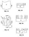
- FIG. 1Ais a top view of a semiconductor substrate used in the first step of the method of present invention to form isolation regions.
- FIG. 1Bis a cross sectional view taken along the line 1 — 1 .
- FIG. 1Cis a top view of the next step in the processing of the structure of FIG. 1B , in which isolation regions are formed.
- FIG. 1Dis a cross sectional view of the structure in FIG. 1C taken along the line 1 — 1 showing the isolation stripes formed in the structure.
- FIG. 1Eis a cross sectional view of the structure in FIG. 1C taken along the line 1 — 1 showing the two types of isolation regions that can be formed in the semiconductor substrate: LOCOS or shallow trench.
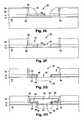
- FIGS. 2A-2Nare cross sectional views taken along the line 2 — 2 of FIG. 1C showing in sequence the next step(s) in the processing of the structure shown in FIG. 1C , in the formation of a non volatile memory array of floating memory cells of the split gate type.
- FIG. 2Ois a top view showing the interconnection of row lines and bit lines to terminals in active regions in the formation of the non volatile memory array of floating memory cells of the split gate type.
- FIGS. 3A-3Iare cross sectional views taken along the line 2 — 2 of FIG. 1C showing in sequence the steps in a first alternate processing of the structure shown in FIG. 1C , in the formation of a non volatile memory array of floating memory cells of the split gate type.
- FIGS. 4A-4Jare cross sectional views taken along the line 2 — 2 of FIG. 1C showing in sequence the steps in a second alternate processing of the structure shown in FIG. 1C , in the formation of a non volatile memory array of floating memory cells of the split gate type.
- FIGS. 5A-5Kare cross sectional views taken along the line 2 — 2 of FIG. 1C showing in sequence the steps in a third alternate processing of the structure shown in FIG. 1C , in the formation of a non volatile memory array of floating memory cells of the split gate type.
- FIG. 1Athere is shown a top plan view of a semiconductor substrate 10 , which is preferably of P type and is well known in the art.
- a first layer of insulation material 12such as silicon dioxide (oxide) is deposited thereon as shown in FIG. 1 B.
- the first insulation layer 12is formed on the substrate 10 by well known techniques such as oxidation or deposition (e.g. chemical vapor deposition or CVD), forming a layer of silicon dioxide (hereinafter “oxide”).
- a first layer of polysilicon 14 (FG poly)is deposited on top of the first layer of insulation material 12 .
- the deposition and formation of the first polysilicon layer 14 on the first insulation layer 12can be made by a well known process such as Low Pressure CVD or LPCVD.
- a silicon nitride layer 18(hereinafter “nitride”) is deposited over the polysilicon layer 14 , preferably by CVD. This nitride layer 18 is used to define the active regions during isolation formation.
- nitridesilicon nitride layer 18
- all of the forgoing described parameters and the parameters described hereinafter,depend upon the design rules and the process technology generation. What is described herein is for the 0.18 micron process. However, it will be understood by those skilled in the art that the present invention is not limited to any specific process technology generation, nor to any specific value in any of the process parameters described hereinafter.
- suitable photo-resistant material 19is applied on the silicon nitride layer 18 and a masking step is performed to selectively remove the photo-resistant material from certain regions (stripes 16 ).
- the silicon nitride 18 , the polysilicon 14 and the underlying insulation material 12are etched away in stripes 16 formed in the Y direction or the column direction, as shown in FIG. 1C , using standard etching techniques (i.e. anisotropic etch process).
- the distance W between adjacent stripes 16can be as small as the smallest lithographic feature of the process used.
- the silicon nitride 18 , the first polysilicon region 14 and the underlying insulation region 12are maintained.
- the resulting structureis illustrated in FIG. 1 D.
- LOCOSlow-oxide-semiconductor
- STIshallow-semiconductor
- the structureis further processed to remove the remaining photo resist 19 .
- an isolation material 20 a or 20 bsuch as silicon dioxide, is formed in the regions or “grooves” 16 .
- the nitride layer 18is then selectively removed to form the structure shown in FIG. 1 E.
- the isolationcan be formed via the well known LOCOS process resulting in the local field oxide 20 a (e.g. by oxidizing the exposed substrate), or it can be formed via a shallow trench process (STI) resulting in silicon-dioxide being formed in the region 20 b (e.g. by depositing an oxide layer, followed by a Chemical-Mechanical-Polishing or CMP etch). It should be noted that during the LOCOS formation, a spacer may be necessary to protect the side walls of poly layer 14 during the formation of the local field oxide.
- STIshallow trench process
- the substrate 10has alternating stripes of active regions and isolation regions with the isolation regions being formed of either LOCOS insulation material 20 a or shallow trench insulation material 20 b .
- FIG. 1Eshows the formation of both a LOCOS region 20 a and a shallow trench region 20 b , only one of the LOCOS process ( 20 a ) or the shallow trench process ( 20 b ) will be used. In the preferred embodiment, the shallow trench 20 b will be formed. Shallow trench 20 b is preferable because it can be more precisely formed at smaller design rules.
- the structure in FIG. 1Erepresents a self aligned structure, which is more compact than a structure formed by a non self-aligned method.
- a non self-aligned method of forming the structure shown in FIG. 1Eis as follows. Regions of isolation 20 are first formed in the substrate 10 . This can be done by depositing a layer of silicon nitride on the substrate 10 , depositing photo-resist, patterning the silicon nitride using a first masking step to expose selective portions of the substrate 10 , and then oxidizing the exposed substrate 10 using either the LOCOS process or the STI process where silicon trench formation and trench fill are involved.
- the silicon nitrideis removed, and a first layer of silicon dioxide 12 (to form the gate oxide) is deposited over the substrate 10 .
- a first layer of polysilicon 14is deposited over the gate oxide 12 .
- the first layer of polysilicon 14is then patterned using a second masking step and selective portions removed.
- the polysilicon 14is not self aligned with the regions of isolation 20 , and a second masking step is required. Further, the additional masking step requires that the dimensions of the polysilicon 14 have an alignment tolerance with respect to the regions of isolation 20 . It should be noted that the non self-aligned method does not utilize nitride layer 18 .
- FIG. 2Ashows the structure from a view orthogonal to that of FIGS. 1B and 1E , the next steps in the process of the present invention are illustrated.
- a thick insulation layer 24such as silicon nitride (hereinafter “nitride”) is formed on the structure, followed by the formation of a thin protective layer 26 such as polysilicon (hereinafter “poly”).
- polypolysilicon
- a conventional photo-lithography masking operationis performed with photo-resist applied on top of the poly layer 26 .
- a masking stepis applied in which stripes (i.e. masking regions) are defined in the X or the row direction. The distance between adjacent stripes can be a size determined by the needs of the device to be fabricated.
- the photo resistis removed in defined masking regions, i.e. stripes in the row direction, after which poly layer 26 underlying the removed photo resist is etched away in the stripes using a conventional anisotropic poly etch process to expose portions of the underlying nitride layer 24 .
- An anisotropic nitride etch processis then performed to remove the exposed portions of nitride layer 24 to expose portions of poly layer 14 .
- An optional poly etch processcan follow to remove just a top portion of the exposed poly layer 14 , to slightly recess poly layer 14 relative to the remaining nitride layer 24 , and to form sloped portions 28 of poly layer 14 where it meets nitride layer 24 .
- these etch processesresult in the formation of a single first trench 30 that extends down to (and preferably slightly into) polysilicon layer 14 .
- the remaining photo-resistis then removed, resulting in the structure shown in FIG. 2 B.
- a layer 32 of insulation material, such as silicon dioxide (hereinafter “oxide”)is then formed over the structure using, for example, a thermal oxidation process.
- oxide layer 32 formed on poly layer 14 in trenches 30have raised portions 34 caused by sloped portions 28 of poly layer 14 , giving oxide layer 32 inside trenches 30 a lens shape.
- FIG. 2 CThe resulting structure is illustrated in FIG. 2 C.
- Insulation spacers 40are then formed inside trenches 30 (FIG. 2 E). Formation of spacers is well known in the art by depositing a material over the contour of a structure, followed by an anisotropic etch process (e.g. RIE), whereby the material is removed from horizontal surfaces of the structure, while the material remains largely intact on vertically oriented surfaces of the structure. Spacers 40 can be formed of any dielectric material. In the preferred embodiment, spacers 40 are formed of nitride in the following manner. A thin layer 36 of insulation material (i.e. oxide) is formed over the structure of FIG. 2C preferably using a conventional chemical vapor deposition (CVD) process. A thick layer 38 of insulation material (i.e.
- CVDchemical vapor deposition
- nitrideis then formed over the structure preferably by a conventional nitride deposition process, as shown in FIG. 2 D.
- a thick nitride etch processthat uses oxide layer 36 as an etch stop.
- This etch processremoves all of nitride layer 38 , except for sidewall spacers 40 along the sidewalls of trenches 30 .
- An anisotropic oxide etch processis then performed that uses poly layer 26 as an etch stop. This oxide etch removes exposed portions of oxide layers 36 and 32 that are over nitride layer 24 .
- the oxide etchalso removes portion of oxide layers 36 and 32 that are exposed in trenches 36 between spacers 40 , to expose portions of poly layer 14 at the centers of the trenches 30 .
- the resulting structureis shown in FIG. 2 E.
- a thick nitride etch processis performed to remove spacers 40 from trenches 30 .
- a poly etch processis then performed to remove poly layer 26 to expose nitride layer 24 , and to remove the exposed portions of poly layer 14 at the bottom center of trenches 30 to expose oxide layer 12 .
- trenches 30each have a narrow lower portion 42 bounded by poly layer 14 and oxide layers 32 and 36 , and an upper wider portion 44 bounded by oxide layer 36 . It should be noted that the spacers 40 can be removed after the poly etch process that removes portions of poly layer 14 .
- Insulation spacers 46are formed on sidewalls of the lower portions 42 of trenches 30 .
- oxide spacer 46 formationis preceded by first forming an insulation sidewall layer 48 (oxide) on the sides of polysilicon layer 14 that are exposed inside trenches 30 (i.e. by oxidizing the structure or by CVD). Then, oxide is formed over the structure (i.e.
- oxide anisotropic etchwhich removes the oxide formed over the structure, except for oxide spacers 46 formed on the sidewalls of lower trench portion 42 .
- This oxide formation and etch processalso adds to the thickness of the vertical portion of oxide layer 36 in upper trench portion 44 .
- the anisotropic etchalso removes a top portion of oxide layer 36 , thins down the portion of oxide layer 36 over oxide layer 32 , as well as removes the portion of oxide layer 12 at the bottom of trenches 30 in between spacers 46 to expose the substrate 10 .
- the resulting structureis shown in FIG. 2 G.
- a conductive layer 52such as titanium nitride which adheres well to the exposed substrate 10 , is formed over the entire structure, which lines the sidewalls of trenches 30 and exposed substrate 10 therein.
- a tungsten etch-back stepfollows to remove any tungsten outside of trenches 30 , and to preferably define the top surfaces of conductive blocks 54 below the tops of oxide layers 36 .
- a conductive layer 56(titanium nitride) is then formed over conductive blocks 54 , preferably by depositing titanium nitride over the structure, followed by a planarizing (CMP) process that removes the deposited titanium nitride except for the conductive layer 56 over conductive blocks 54 in trenches 30 .
- CMPplanarizing
- a titanium nitride etchis then performed so that conductive layer 56 is recessed below the top of oxide layer 36 .
- a layer 58 of insulation material (oxide)is then formed over the structure, followed by a planarization process (CMP) and oxide etch process to remove the deposited oxide except for that portion over conductive layer 56 .
- CMPplanarization process
- Second trenches 63are formed between pair sets of memory cells and adjacent to first trenches 30 in the following manner.
- Nitride layer 24is removed, preferably using an isotropic etch process, to expose portions of poly layer 14 and oxide layer 32 as shown in FIG. 2I.
- a poly etch processfollows (i.e. a dry etch) to remove exposed portions of poly layer 14 and to expose oxide layer 12 .
- the exposed portions of oxide layer 12are then removed via a controlled oxide etch, exposing substrate 10 .
- An insulation layer 64preferably oxide, is then formed over the entire structure, resulting in the structure shown in FIG. 2 J.
- the raised portions 34 of oxide layer 32result in the formation of upwardly extending sharp edges 66 of poly layer 14 where layer 14 meets oxide layer 64 .
- Control gate poly blocksare formed in second trenches 63 in the following manner.
- a thick layer of polysiliconis deposited over the structure, followed by an anisotropic poly etch process, which removes all the deposited polysilicon except for poly spacers (blocks) 68 formed against vertically oriented portions of oxide layer 64 .
- Poly blocks 68have lower portions 70 disposed immediately adjacent to poly layer 14 , and upper portions 72 that extend over a portion of the poly layer 14 including sharp edge 66 .
- Poly blocks 68are insulated from poly layer 14 by oxide layers 64 and 32 . The resulting structure is illustrated in FIG. 2 K.
- Insulation spacers 74are then formed adjacent to poly blocks 68 , and are made of one or more layers of material.
- insulation spacers 74are made of two layers of material by first depositing a thin layer 76 of oxide, followed by the deposition of nitride over the structure. An anisotropic nitride etch is performed to remove the deposited nitride, leaving nitride spacers 78 . Ion implantation (e.g. N+) is then used to form second regions (terminals) 80 in the substrate in the same manner as the first regions 50 were formed. A controlled oxide etch follows, which removes the exposed portions of oxide layer 76 , as well as the exposed portions of oxide layer 64 to expose substrate 10 and the second regions 80 . The resulting structure is shown in FIG. 2 L.
- a layer of metalized silicon (silicide) 82is formed in the top of the substrate 10 next to side wall spacers 74 , along with a layer of metalized silicon 84 over poly blocks 68 , by depositing a metal such as tungsten, cobalt, titanium, nickel, platinum, or molybdenum over the structure.
- the structureis then annealed, permitting the hot metal to flow and to seep into the exposed top portions of the substrate to form silicide 82 , and into the exposed top portions of poly blocks 68 to form metalized silicon 84 .
- the metal deposited on the remaining structureis removed by a metal etch process.
- Metalized silicon region 82 on substrate 10can be called self aligned silicide (i.e. salicide), because it is self aligned to the second regions 80 by spacers 78 .
- the resulting structureis shown in FIG. 2 M.
- Passivationsuch as BPSG 86
- a masking stepis performed to define etching areas over the silicide regions 82 .
- the BPSG 86is selectively etched in the masked regions to create contact openings that are ideally centered over and extend down to silicide regions 82 formed between adjacent sets of paired memory cells.
- the contact openingsare then filled with a conductor metal by metal deposition and planarization etch-back to form contact conductors 88 .
- the silicide layers 82facilitate conduction between the conductors 88 and second regions 80 .
- a bit line 90is added by metal masking over the BPSG 86 , to connect together all the conductors 88 in the column of memory cells.
- the final memory cell structureis illustrated in FIG. 2 N.
- first and second regions 50 / 80form the source and drain for each cell (those skilled in the art know that source and drain can be switched during operation).
- the channel region 92 for each cellis the portion of the substrate that is in-between the source and drain 50 / 80 .
- Poly blocks 68constitute the control gate, and poly layer 14 constitutes the floating gate.
- Oxide layers 32 , 36 , 46 and 48together form an insulation layer that is disposed adjacent to and over floating gate 14 , to isolate it from conductive block 54 and conductive layer 52 .
- Oxide layers 36 and 64together form an insulation layer that isolates the conductive block 54 and conductive layer 52 from the control gates 68 .
- control gates 68have one side aligned to the edge of the second region 80 , and are disposed over part of the channel regions 92 .
- Control gates 68have lower portions 70 that are disposed adjacent to the floating gates 14 (insulated therefrom by oxide layer 64 ), and upper protruding portions 72 that are disposed (extend) over a portion of adjacent poly layers 14 (insulated therefrom by oxide layers 64 ).
- a notch 94is formed by the protruding portion 72 , where the sharp edge 66 of floating gate 14 extends into the notch 94 .
- Each floating gate 14is disposed over part of the channel region 92 , is partially overlapped at one end by the control gate 68 , and partially overlaps the first region 50 with its other end.
- Conductive blocks 54 and the conductive layers 52 / 56together form source lines 96 that extend across the columns of memory cells. Upper portions 62 of source lines 96 extend over but are insulated from the floating gates 14 , while lower portions 60 of source lines 96 are adjacent to but insulated from floating gates 14 . As illustrated in the FIG. 2N , the process of the present invention forms pairs of memory cells that mirror each other. The pairs of mirrored memory cells are insulated from other cell pairs by oxide layer 76 , nitride spacers 78 and BPSG 86 .
- FIG. 2Othere is shown a top plan view of the resulting structure and the interconnection of the bit lines 90 to the second regions 80 , of the control lines 68 which run in the X or the row direction, and of the source lines 96 which connect to the first regions 50 within the substrate 10 .
- the source lines 96make contact with the substrate 10 in the entire row direction, i.e. contact with the active regions as well as the isolation regions, the source lines 96 electrically connect only to the first regions 50 in the substrate 10 .
- each first region 50 to which the “source ” line 96 is connectedis shared between two adjacent memory cells.
- each second region 80 to which the bit line 90 is connectedis shared between adjacent memory cells from different mirror sets of memory cells.
- the resultis a plurality of non volatile memory cells of the split gate type having a floating gate 14 , a control gate 68 which is immediately adjacent to but separated from the floating gate 14 and runs along the length of the row direction connecting to the control gates of other memory cells in the same row, a source line 96 which also runs along the row direction, connecting pairs of the first regions 50 of the memory cells in the same row direction, and a bit line 90 which runs along the column or Y direction and connects pairs of the second regions 80 of the memory cells in the same column direction.
- the formation of the control gate, the floating gate, the source line, and the bit line,are all self-aligned.
- the non-volatile memory cellis of the split gate type having floating gate to control gate tunneling all as described in U.S. Pat. No. 5,572,054, whose disclosure is incorporated herein by reference with regard to the operation of such a non-volatile memory cell and an array formed thereby.
- the present inventionexhibits reduced source line resistance because of the wider upper portion 62 of T-shaped conductive block 52 , while still providing for smaller scaling of memory cell dimensions due to the narrower lower portions 60 of T-shaped conductive blocks 52 (i.e. the indentation of the sidewalls of the first trenches 30 between upper and lower portions 62 / 60 that forms the T-shape of the source line).
- the upper portions 62also extend over but are insulated from the floating gates 14 which allows coupling of source voltage from the source line 96 to the floating gates 14 through the oxide layers 32 / 36 (which is in addition to the coupling via the lower portions 60 through oxide layers 46 / 48 , and via first region 50 through oxide layer 12 ).
- the coupling coefficient between the source electrode and the floating gateis enhanced.
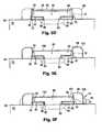
- FIGS. 3A-3Iillustrate a first alternate process for forming a memory cell array similar to that illustrated in FIG. 2N , but with a polysilicon source line.
- This first alternate processbegins with the same structure as shown in FIG. 2G , but continues as follows.
- Conductive blocks 98are formed inside trenches 30 , preferably by depositing a conductive material such as polysilicon over the structure, followed by a poly planarization process (preferably CMP) to remove polysilicon above trenches 30 .
- a poly etch-back stepfollows to remove any polysilicon outside of trenches 30 , and to recess the top surfaces of conductive blocks 98 below the tops of oxide layers 36 .
- the poly blocks 98can be in-Situ doped or doped using implantation.
- a layer 58 of insulation materialis then formed over poly blocks 98 , for example by thermal oxidation, or by oxide deposition followed by a CMP planarization process and an oxide etch process so that oxide layer 58 is recessed below the top of oxide layer 36 .
- the resulting structureis shown in FIG. 3A , where the narrow/wide trench portions 42 / 44 result in substantially T-shaped conductive poly blocks 98 with narrow lower block portions 60 and wider upper block portions 62 .
- Second trenches 63are formed between pair sets of memory cells and adjacent to first trenches 30 in the following manner.
- Nitride layer 24is removed, preferably using an isotropic etch process, to expose portions of poly layer 14 and oxide layer 32 as shown in FIG. 3B.
- a poly etch processfollows (i.e. a dry etch) to remove exposed portions of poly layer 14 and to expose portions of oxide layer 12 .
- the exposed portions of oxide layer 12are then removed via a controlled oxide etch, exposing substrate 10 .
- An insulation layer 64preferably oxide, is then formed over the entire structure, resulting in the structure shown in FIG. 3 C.
- the raised portions 34 of oxide layer 32result in the formation of upwardly extending sharp edges 66 of poly layer 14 where layer 14 meets oxide layer 64 .
- Control gate poly blocksare formed in second trenches 63 in the following manner.
- a thick layer of polysiliconis deposited over the structure, followed by an anisotropic poly etch process, which removes all the deposited polysilicon except for poly spacers (blocks) 68 formed against vertically oriented portions of oxide layer 64 .
- Poly blocks 68have lower portions 70 disposed immediately adjacent to poly layer 14 , and upper portions 72 that extend over a portion of the poly layers 14 including sharp edges 66 .
- Poly blocks 68are insulated from poly layer 14 by oxide layers 64 and 32 . The resulting structure is illustrated in FIG. 3 D.
- An oxide etchis performed to remove exposed portions of oxide layer 64 , and the underlying oxide layer 58 , to expose poly blocks 98 and substrate 10 .
- a dry-etch process with end-point detectionis used, which also removes the upper portions of oxide layer 36 , so that it is substantially even with the top surface of poly blocks 98 .
- An oxide deposition processfollows to form an oxide layer 100 over the structure, and to replace oxide layer 64 over the substrate 10 . The resulting structure is illustrated in FIG. 3 E.
- Insulation spacers 74are then formed adjacent to poly blocks 68 , and are made of one or more layers of material.
- insulation spacers 74are composite spacers that include lower portions of oxide layer 100 and nitride spacers 78 formed by the deposition of nitride over the structure followed by an anisotropic nitride etch to remove the deposited nitride (using the oxide layer 100 as an etch stop), leaving nitride spacers 78 over oxide layer 64 and adjacent to poly spacers 68 .
- Nitride spacers 101are also formed over the ends of conductive blocks 98 , as shown in FIG. 3 F.
- Ion implantatione.g. N+
- Ion implantationis then used to form second regions (terminals) 80 in the substrate in the same manner as the first regions 50 were formed.
- a controlled oxide etchfollows to remove the exposed portions of oxide layer 100 to expose poly blocks 98 , and to remove exposed portions of oxide layer 64 to expose the substrate 10 .
- the resulting structureis shown in FIG. 3 G.
- a layer of metalized silicon (silicide) 82is formed in the top of the substrate 10 next to side wall spacers 74 , along with a layer of metalized silicon 84 over poly blocks 68 and poly block 98 , by depositing a metal such as tungsten, cobalt, titanium, nickel, platinum, or molybdenum over the structure.
- the structureis then annealed, permitting the hot metal to flow and to seep into the exposed top portions of the substrate to form silicide 82 , and into the exposed top portions of poly blocks 68 and 98 to form metalized silicon 84 .
- the metal deposited on the remaining structureis removed by a metal etch process.
- Metalized silicon region 82 on substrate 10can be called self aligned silicide (i.e. salicide), because it is self aligned to the second regions 80 by spacers 78 .
- the resulting structureis shown in FIG. 3 H.
- Passivationsuch as BPSG 86
- a masking stepis performed to define etching areas over the silicide regions 82 .
- the BPSG 86is selectively etched in the masked regions to create contact openings that are ideally centered over and extend down to silicide regions 82 formed between adjacent sets of paired memory cells.
- the contact openingsare then filled with a conductor metal by metal deposition and planarization etch-back to form contact conductors 88 .
- the silicide layers 82facilitate conduction between the conductors 88 and second regions 80 .
- a bit line 90is added by metal masking over the BPSG 86 , to connect together all the conductors 88 in the column of memory cells.
- the final memory cell structureis illustrated in FIG. 3 I.
- the first alternate embodimentexhibits reduced source line resistance because of the wider upper portion 62 of T-shaped poly block 98 and the highly conductive metalized silicon layer 84 formed thereon, while still providing for smaller scaling of memory cell dimensions due to the narrower lower portion 60 of T-shaped conductive block 98 .
- the upper portions 62also extend over the floating gate 14 which allows coupling of source voltage from the poly block 98 to the floating gate 14 through the oxide layers 32 / 36 (in addition to the coupling through the oxide layers 46 / 48 via lower portions 60 , and through the oxide layer 12 via first region 50 ).
- the coupling coefficient between the source electrode and the floating gateis enhanced.
- FIGS. 4A-4Iillustrate a second alternate process for forming a memory cell array similar to that illustrated in FIG. 2N , but utilizing a self aligned contact scheme.
- This second alternate processbegins with the same structure as shown in FIG. 2J , but continues as follows.
- a layer of nitride 104is then deposited over the structure, followed by a nitride planarization process (e.g. CMP).
- a nitride etch-back stepfollows to remove the portions of nitride layer 104 over the raised portions of poly layer 102 , while leaving portions of nitride layer 104 over the flat side portions of poly layer 102 .
- An oxidation stepfollows, which oxidizes the exposed center portions of poly layer 102 to form a layer of oxide 106 thereover. The resulting structure is shown in FIG. 4 B.
- Nitride layer 104is removed by a nitride etch process, which is followed by an anisotropic poly etch step to remove those portions of poly layer 102 not directly under oxide layer 106 , as illustrated in FIG. 4 C.
- An oxide deposition stepis then performed to apply a thick oxide layer over the structure. This is followed by a planarizing oxide etch, such as CMP, to planarize the structure using poly layer 102 as an etch stop.
- a planarizing oxide etchsuch as CMP
- An oxide etch-back stepis then performed, leaving blocks 108 of oxide on either side of the poly layer 102 .
- Oxide layer 106is also removed by the oxide planarizing and etch-back steps, resulting in the structure shown in FIG. 4D.
- a planarizing poly etch, such as CMPis then performed using the oxide blocks 108 as an etch stop, as illustrated in FIG. 4 E.
- Poly blocks 103have lower portions 70 disposed immediately adjacent to poly layer 14 , and upper portions 72 that extend over a portion of the poly layer 14 including sharp edge 66 .
- Poly blocks 103are insulated from poly layer 14 by oxide layers 64 and 32 . Oxide blocks 108 and oxide layer 36 are left to extend well above the top surface of poly blocks 103 , as illustrated in FIG. 4 F.
- An optional implant stepcan be performed to dope the exposed poly blocks 103 .
- a metal deposition stepis then performed, to deposit a metal such as tungsten, cobalt, titanium, nickel, platinum, or molybdenum over the structure.
- the structureis then annealed, permitting the hot metal to flow and to seep into the exposed top portions of the poly blocks 103 to form a conductive layer of metalized silicon 84 thereon.
- the metal deposited on the remaining structureis removed by a metal etch process.
- Metalized silicon layer 84can be called self aligned because it is self aligned to the poly blocks 103 by oxide layer 64 and oxide blocks 108 .
- a protective nitride layer 110is formed over poly blocks 103 and between oxide blocks 108 in the following manner.
- Nitrideis deposited over the structure, followed by a planarizing nitride etch, such as CMP, with oxide blocks 108 used as the etching stop layer, so that nitride layer 110 is level with oxide blocks 108 .
- the nitride layer 110is self aligned to the poly blocks 103 by oxide blocks 108 .
- the resulting structureis shown in FIG. 4 G.
- Insulation spacers 74are then formed adjacent to poly blocks 103 and nitride layer 110 , and are made of one or more layers of material. In the preferred embodiment, insulation spacers 74 are made of two layers of material by first depositing a thin layer 76 of oxide, followed by the deposition of a nitride over the structure. An anisotropic nitride etch is performed to remove the deposited nitride, leaving nitride spacers 78 . Ion implantation (e.g. N+) is then used to form second regions (terminals) 80 in the substrate in the same manner as the first regions 50 were formed.
- Ion implantatione.g. N+
- a layer of metalized silicon (silicide) 82is formed in the top of the substrate 10 next to side wall spacers 74 , by depositing a metal such as tungsten, cobalt, titanium, nickel, platinum, or molybdenum over the structure. The structure is then annealed, permitting the hot metal to flow and to seep into the exposed top portions of the substrate 10 to form silicide regions 82 . The metal deposited on the remaining structure is removed by a metal etch process. Metalized silicon region 82 on substrate 10 can be called self aligned silicide (i.e. salicide), because it is self aligned to the second regions 80 by spacers 78 . The resulting structure is shown in FIG. 4 I.
- Passivationsuch as BPSG 86
- a masking stepis performed to define etching areas over the salicide regions 82 .
- the BPSG 86is selectively etched in the masked regions to create contact openings that are ideally centered over and wider than the salicide regions 82 formed between adjacent sets of paired memory cells.
- Nitride layer 110serves to protect poly blocks 103 and metalized silicon 84 from this etch process.
- the contact openingsare then filled with a conductor metal by metal deposition and planarizing etch-back, whereby the entire area between nitride spacers 78 of adjacent sets of paired memory cells is filled with the deposited metal to form contact conductors 88 that are self aligned to the salicide regions 82 by the nitride spacers 78 (i.e. self aligned contact scheme, or SAC).
- the salicide layers 82facilitate conduction between the conductors 88 and second regions 80 .
- a bit line 90is added by metal masking over the BPSG 86 , to connect together all the conductors 88 in the column of memory cells.
- the final memory cell structureis illustrated in FIG. 4 J.
- the self aligned contact schemeremoves an important constraint on the minimum spacing requirement between adjacent sets of paired memory cells.
- FIG. 4Jillustrates the contact area (and thus conductors 88 ) perfectly centered over the salicide regions 82 , in reality it is very difficult to form the contact openings without some undesirable horizontal shift relative to the salicide regions 82 .
- electrical shortscan occur if the contact 88 is shifted over and formed over metalized silicon 84 and poly block 103 .
- the contact openingswould have to be formed sufficiently away from the nitride spacers 78 so that even with the maximum possible shift in the contact regions, they will not extend to nitride spacers 78 or beyond. This of course would present a constraint on the minimum distance between spacers 78 , in order to provide a sufficient tolerance distance between adjacent sets of paired mirror cells.
- the SAC method of the present inventioneliminates this constraint by using the protective layer of material (nitride layer 110 ) underneath the BPSG.
- the contact openingsare formed in the BPSG with a sufficient width to ensure there is overlap of the contact opening with the salicide regions 82 , even if there is a significant horizontal shift of the contact opening during formation.
- Nitride layer 110allows portions of contact 88 to be formed over poly block 103 or metalized silicon layer 84 , without any shorting therebetween.
- the wide contact openingguarantees that contacts 88 completely fill the very narrow spaces between spacers 78 , and make good electrical contact with salicide regions 82 .
- the width of contact regions between spacers 78can be minimized, while preventing faulty connections by filling the space between spacers 78 , allowing the scaling down of the overall cell dimension.
- control gates 103are substantially rectangularly shaped with a protruding portion 72 over the floating gate 14 , and a planar opposing surface that facilitates the formation of spacers 74 , which in turn facilitates the self aligned formation of the salicide regions 82 , and the formation of the self aligned conductor 88 .
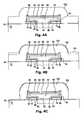
- FIGS. 5A-5Killustrate a third alternate process for forming a memory cell array similar to that illustrated in FIG. 3I , but utilizing a self aligned contact scheme.
- This third alternate processbegins with the same structure as shown in FIG. 3C , but continues as follows.
- a layer of nitride 104is then deposited over the structure, followed by a nitride planarization process (e.g. CMP).
- a nitride etch-back stepfollows to remove the portions of nitride layer 104 over the raised portions of poly layer 102 , while leaving portions of nitride layer 104 over the flat side portions of poly layer 102 .
- An oxidation stepfollows, which oxidizes the exposed center portions of poly layer 102 to form a layer of oxide 106 thereover. The resulting structure is shown in FIG. 5 B.
- Nitride layer 104is removed by a nitride etch process, which is followed by an anisotropic poly etch step to remove those portions of poly layer 102 not directly under oxide layer 106 , as illustrated in FIG. 5 C.
- An oxide deposition stepis then performed to apply a thick oxide layer 108 over the structure. This is followed by a planarizing oxide etch, such as CMP, to planarize the structure using poly layer 102 as an etch stop. An oxide etch-back step is then performed, leaving blocks 108 of oxide on either side of the poly layer 102 . Oxide layer 106 is also removed by the oxide planarizing and etch-back steps.
- a nitride deposition stepis then performed to apply a nitride layer over the structure. This is followed by a planarizing nitride etch, such as CMP, to planarize the structure using poly layer 102 as an etch stop. A nitride etch-back step is then performed, leaving nitride layer 109 over oxide blocks 108 . The resulting structure is shown in FIG. 5 D.
- a planarizing poly etchsuch as CMP, is then performed using the nitride layer 109 as an etch stop, as illustrated in FIG. 5 E.
- a poly etch-back processsuch as RIE, to remove the top portions of poly layer 102 leaving just poly blocks 103 adjacent oxide blocks 108 , and exposing oxide layer 64 .
- Poly blocks 103have lower portions 70 disposed immediately adjacent to poly layer 14 , and upper portions 72 that extend over a portion of the poly layer 14 including sharp edge 66 .
- Poly blocks 103are insulated from poly layer 14 by oxide layers 64 and 32 . Oxide blocks 108 and oxide layer 36 are left to extend well above the top surface of poly blocks 103 , as illustrated in FIG. 5 F.
- a controlled oxide etchis performed to remove exposed horizontal portions of oxide layer 64 , and the underlying oxide layer 58 , to expose poly blocks 98 .
- a dry-etch process with end-point detectionis used, which also removes the upper portions of oxide layer 36 , as illustrated in FIG. 5 G.
- An optional implant stepcan be performed to dope the exposed poly blocks 103 .
- a metal deposition stepis then performed, to deposit a metal such as tungsten, cobalt, titanium, nickel, platinum, or molybdenum over the structure.
- the structureis then annealed, permitting the hot metal to flow and to seep into the exposed top portions of the poly blocks 103 and 98 to form a conductive layer of metalized silicon 84 thereon.
- the metal deposited on the remaining structureis removed by a metal etch process.
- Metalized silicon layer 84can be called self aligned because it is self aligned to the poly blocks 103 by oxide layer 64 and oxide blocks 108 .
- a protective nitride layer 110is formed over poly blocks 103 and between oxide blocks 108 in the following manner.
- Nitrideis deposited over the structure, followed by a planarizing nitride etch, such as CMP, with oxide blocks 108 used as the etching stop layer, so that nitride layer 110 is level with oxide blocks 108 . Nitride layer 109 is also removed by this process. The nitride layer 110 is self aligned to the poly blocks 103 by oxide blocks 108 . The resulting structure is shown in FIG. 5 H.
- Insulation spacers 74are then formed adjacent to poly blocks 103 and nitride layer 110 , and are made of one or more layers of material. In the preferred embodiment, insulation spacers 74 are made of two layers of material by first depositing a thin layer 76 of oxide, followed by the deposition of a nitride over the structure. An anisotropic nitride etch is performed using oxide layer 76 as an etch stop to remove the deposited nitride except for nitride spacers 78 . Ion implantation (e.g.
- N+is then used to form second regions (terminals) 80 in the substrate in the same manner as the first regions 50 were formed.
- An oxide etchfollows, which removes the exposed portions of oxide layer 76 .
- a layer of metalized silicon (silicide) 82is formed in the top of the substrate 10 next to side wall spacers 74 , by depositing a metal such as tungsten, cobalt, titanium, nickel, platinum, or molybdenum over the structure. The structure is then annealed, permitting the hot metal to flow and to seep into the exposed top portions of the substrate 10 to form silicide regions 82 . The remaining metal deposited on the remaining structure is removed by a metal etch process.
- Metalized silicon region 82 on substrate 10can be called self aligned silicide (i.e. salicide), because it is self aligned to the second regions 80 by spacers 78 .
- the resulting structureis shown in FIG. 5 J.
- Passivationsuch as BPSG 86
- a masking stepis performed to define etching areas over the salicide regions 82 .
- the BPSG 86is selectively etched in the masked regions to create contact openings that are ideally centered over and wider than the salicide regions 82 formed between adjacent sets of paired memory cells.
- Nitride layer 110serves to protect poly blocks 103 and metalized silicon layers 84 from this etch process.
- the contact openingsare then filled with a conductor metal by metal deposition and planarizing etch-back, whereby the entire area between nitride spacers 78 of adjacent sets of paired memory cells is filled with the deposited metal to form contact conductors 88 that are self aligned to the salicide regions 82 by the nitride spacers 78 (i.e. self aligned contact scheme, or SAC).
- the salicide layers 82facilitate conduction between the conductors 88 and second regions 80 .
- a bit line 90is added by metal masking over the BPSG 86 , to connect together all the conductors 88 in the column of memory cells.
- the final memory cell structureis illustrated in FIG. 5 K.
- the third alternate embodimenthas the advantage of combining the advantages of the first alternate embodiment, with the advantages of SAC.
- first trench upper and lower portionsneed not be symmetrical, but rather the first trenches need only have an indentation in the sidewall thereof so that the source line formed therein has a first portion disposed adjacent to the floating gate, and a second portion disposed over the floating gate.
Landscapes
- Semiconductor Memories (AREA)
- Non-Volatile Memory (AREA)
Abstract
Description
- the first block includes a lower portion formed in the lower portion of the first trench that is disposed adjacent to and insulated from the first layer of conductive material, and
- the first block includes an upper portion formed in the upper portion of the first trench that is disposed over and insulated from the first layer of conductive material;
- the first block includes a lower portion formed below the indentation of the first trench sidewall that is disposed adjacent to and insulated from the first layer of conductive material, and
- the first block includes an upper portion formed above the indentation of the first trench sidewall that is disposed over and insulated from the first layer of conductive material;
Claims (8)
Priority Applications (1)
| Application Number | Priority Date | Filing Date | Title |
|---|---|---|---|
| US10/690,204US6855980B2 (en) | 2000-09-20 | 2003-10-20 | Semiconductor memory array of floating gate memory cells with low resistance source regions and high source coupling |
Applications Claiming Priority (7)
| Application Number | Priority Date | Filing Date | Title |
|---|---|---|---|
| US23431400P | 2000-09-20 | 2000-09-20 | |
| US24209600P | 2000-10-19 | 2000-10-19 | |
| US26016701P | 2001-01-05 | 2001-01-05 | |
| US27551701P | 2001-03-12 | 2001-03-12 | |
| US28704701P | 2001-04-26 | 2001-04-26 | |
| US09/916,555US6727545B2 (en) | 2000-09-20 | 2001-07-26 | Semiconductor memory array of floating gate memory cells with low resistance source regions and high source coupling |
| US10/690,204US6855980B2 (en) | 2000-09-20 | 2003-10-20 | Semiconductor memory array of floating gate memory cells with low resistance source regions and high source coupling |
Related Parent Applications (1)
| Application Number | Title | Priority Date | Filing Date |
|---|---|---|---|
| US09/916,555ContinuationUS6727545B2 (en) | 2000-09-20 | 2001-07-26 | Semiconductor memory array of floating gate memory cells with low resistance source regions and high source coupling |
Publications (2)
| Publication Number | Publication Date |
|---|---|
| US20040084717A1 US20040084717A1 (en) | 2004-05-06 |
| US6855980B2true US6855980B2 (en) | 2005-02-15 |
Family
ID=27559246
Family Applications (2)
| Application Number | Title | Priority Date | Filing Date |
|---|---|---|---|
| US09/916,555Expired - LifetimeUS6727545B2 (en) | 2000-09-20 | 2001-07-26 | Semiconductor memory array of floating gate memory cells with low resistance source regions and high source coupling |
| US10/690,204Expired - LifetimeUS6855980B2 (en) | 2000-09-20 | 2003-10-20 | Semiconductor memory array of floating gate memory cells with low resistance source regions and high source coupling |
Family Applications Before (1)
| Application Number | Title | Priority Date | Filing Date |
|---|---|---|---|
| US09/916,555Expired - LifetimeUS6727545B2 (en) | 2000-09-20 | 2001-07-26 | Semiconductor memory array of floating gate memory cells with low resistance source regions and high source coupling |
Country Status (5)
| Country | Link |
|---|---|
| US (2) | US6727545B2 (en) |
| EP (1) | EP1191586A2 (en) |
| JP (1) | JP5027365B2 (en) |
| KR (1) | KR100855885B1 (en) |
| CN (1) | CN1222992C (en) |
Cited By (21)
| Publication number | Priority date | Publication date | Assignee | Title |
|---|---|---|---|---|
| US20050036393A1 (en)* | 2003-07-02 | 2005-02-17 | Ching-Shi Jenq | Scalable flash EEPROM memory cell with notched floating gate and graded source region, and method of manufacturing the same |
| US20070066009A1 (en)* | 2005-09-19 | 2007-03-22 | International Business Machines Corporation | Sidewall image transfer (sit) technologies |
| US20080100043A1 (en)* | 2006-11-01 | 2008-05-01 | Autoliv Development Ab | Side airbag module with an internal guide fin |
| US8138524B2 (en) | 2006-11-01 | 2012-03-20 | Silicon Storage Technology, Inc. | Self-aligned method of forming a semiconductor memory array of floating memory cells with source side erase, and a memory array made thereby |
| US8711636B2 (en) | 2011-05-13 | 2014-04-29 | Silicon Storage Technology, Inc. | Method of operating a split gate flash memory cell with coupling gate |
| US9525037B2 (en) | 2012-10-18 | 2016-12-20 | United Microelectronics Corporation | Fabricating method of trench gate metal oxide semiconductor field effect transistor |
| US10418451B1 (en) | 2018-05-09 | 2019-09-17 | Silicon Storage Technology, Inc. | Split-gate flash memory cell with varying insulation gate oxides, and method of forming same |
| US10600794B2 (en) | 2018-01-05 | 2020-03-24 | Silicon Storage Technology, Inc. | Twin bit non-volatile memory cells with floating gates in substrate trenches |
| US10838652B2 (en) | 2018-08-24 | 2020-11-17 | Silicon Storage Technology, Inc. | Programming of memory cell having gate capacitively coupled to floating gate |
| US10879252B2 (en) | 2018-01-05 | 2020-12-29 | Silicon Storage Technology, Inc. | Non-volatile memory cells with floating gates in dedicated trenches |
| US20200411673A1 (en)* | 2016-04-20 | 2020-12-31 | Silicon Storage Technology, Inc. | Method of forming pairs of three-gate non-volatile flash memory cells using two polysilicon deposition steps |
| US10991433B2 (en) | 2019-09-03 | 2021-04-27 | Silicon Storage Technology, Inc. | Method of improving read current stability in analog non-volatile memory by limiting time gap between erase and program |
| US10998325B2 (en) | 2018-12-03 | 2021-05-04 | Silicon Storage Technology, Inc. | Memory cell with floating gate, coupling gate and erase gate, and method of making same |
| US11309042B2 (en) | 2020-06-29 | 2022-04-19 | Silicon Storage Technology, Inc. | Method of improving read current stability in analog non-volatile memory by program adjustment for memory cells exhibiting random telegraph noise |
| US11404545B2 (en) | 2019-07-04 | 2022-08-02 | Silicon Storage Technology, Inc. | Method of forming split-gate flash memory cell with spacer defined floating gate and discretely formed polysilicon gates |
| US11769558B2 (en) | 2021-06-08 | 2023-09-26 | Silicon Storage Technology, Inc. | Method of reducing random telegraph noise in non-volatile memory by grouping and screening memory cells |
| US12080355B2 (en) | 2021-06-02 | 2024-09-03 | Silicon Storage Technology, Inc. | Method of improving read current stability in analog non-volatile memory by post-program tuning for memory cells exhibiting random telegraph noise |
| WO2025122183A1 (en) | 2023-12-04 | 2025-06-12 | Silicon Storage Technology, Inc. | Program speed compensation for non-volatile memory cells |
| WO2025151138A1 (en) | 2024-01-12 | 2025-07-17 | Silicon Storage Technology, Inc. | Coarse and fine programming of non-volatile memory cells |
| WO2025188339A1 (en) | 2024-03-08 | 2025-09-12 | Silicon Storage Technology, Inc. | Sequential erase for tuning the program state of non-volatile memory cells |
| WO2025198607A1 (en) | 2024-03-20 | 2025-09-25 | Silicon Storage Technology, Inc. | Semiconductor device with non-planar mosfet device die and planar mosfet device die |
Families Citing this family (37)
| Publication number | Priority date | Publication date | Assignee | Title |
|---|---|---|---|---|
| KR100455379B1 (en)* | 2002-02-21 | 2004-11-06 | 삼성전자주식회사 | Method for fabricating flash memory |
| US6734055B1 (en)* | 2002-11-15 | 2004-05-11 | Taiwan Semiconductor Manufactoring Company | Multi-level (4 state/2-bit) stacked gate flash memory cell |
| KR100823694B1 (en)* | 2002-11-21 | 2008-04-21 | 삼성전자주식회사 | Method of forming floating gate structure of nonvolatile memory device |
| KR100481871B1 (en)* | 2002-12-20 | 2005-04-11 | 삼성전자주식회사 | Non-volatile memory cells having floating gate and method of forming the same |
| US6706599B1 (en)* | 2003-03-20 | 2004-03-16 | Motorola, Inc. | Multi-bit non-volatile memory device and method therefor |
| US7183163B2 (en)* | 2003-04-07 | 2007-02-27 | Silicon Storage Technology, Inc. | Method of manufacturing an isolation-less, contact-less array of bi-directional read/program non-volatile floating gate memory cells with independent controllable control gates |
| US7759719B2 (en)* | 2004-07-01 | 2010-07-20 | Chih-Hsin Wang | Electrically alterable memory cell |
| US7613041B2 (en)* | 2003-06-06 | 2009-11-03 | Chih-Hsin Wang | Methods for operating semiconductor device and semiconductor memory device |
| US7550800B2 (en)* | 2003-06-06 | 2009-06-23 | Chih-Hsin Wang | Method and apparatus transporting charges in semiconductor device and semiconductor memory device |
| US7105406B2 (en)* | 2003-06-20 | 2006-09-12 | Sandisk Corporation | Self aligned non-volatile memory cell and process for fabrication |
| US6890821B2 (en) | 2003-07-11 | 2005-05-10 | Taiwan Semiconductor Manufacturing Co., Ltd. | Method and system for forming source regions in memory devices |
| US6911704B2 (en)* | 2003-10-14 | 2005-06-28 | Advanced Micro Devices, Inc. | Memory cell array with staggered local inter-connect structure |
| US6960506B2 (en)* | 2003-11-13 | 2005-11-01 | Macronix International Co., Ltd. | Method of fabricating a memory device having a self-aligned contact |
| DE10356285A1 (en) | 2003-11-28 | 2005-06-30 | Infineon Technologies Ag | Integrated semiconductor memory and method for manufacturing an integrated semiconductor memory |
| KR100526478B1 (en)* | 2003-12-31 | 2005-11-08 | 동부아남반도체 주식회사 | Semiconductor device and fabricating method thereof |
| US7315056B2 (en) | 2004-06-07 | 2008-01-01 | Silicon Storage Technology, Inc. | Semiconductor memory array of floating gate memory cells with program/erase and select gates |
| US20080203464A1 (en)* | 2004-07-01 | 2008-08-28 | Chih-Hsin Wang | Electrically alterable non-volatile memory and array |
| KR100591768B1 (en)* | 2004-07-12 | 2006-06-26 | 삼성전자주식회사 | Memory Devices and Formation Methods |
| JP2006032950A (en)* | 2004-07-12 | 2006-02-02 | Samsung Electronics Co Ltd | Memory device and method for forming the same |
| KR100621553B1 (en) | 2004-09-22 | 2006-09-19 | 삼성전자주식회사 | Nonvolatile Memory Device and Manufacturing Method Thereof |
| JP2006093707A (en)* | 2004-09-22 | 2006-04-06 | Samsung Electronics Co Ltd | Semiconductor device and manufacturing method thereof |
| KR100598047B1 (en)* | 2004-09-30 | 2006-07-07 | 삼성전자주식회사 | Nonvolatile Memory Device and Manufacturing Method Thereof |
| KR100645063B1 (en)* | 2005-03-14 | 2006-11-10 | 삼성전자주식회사 | Nonvolatile Memory and Manufacturing Method Thereof |
| US7411244B2 (en)* | 2005-06-28 | 2008-08-12 | Chih-Hsin Wang | Low power electrically alterable nonvolatile memory cells and arrays |
| CN100446186C (en)* | 2006-10-09 | 2008-12-24 | 上海华虹Nec电子有限公司 | Floating grid preparation method used for grid dividing structure flash memory |
| US8072023B1 (en) | 2007-11-12 | 2011-12-06 | Marvell International Ltd. | Isolation for non-volatile memory cell array |
| US8120088B1 (en) | 2007-12-07 | 2012-02-21 | Marvell International Ltd. | Non-volatile memory cell and array |
| CN101777519B (en)* | 2010-01-12 | 2013-09-25 | 上海宏力半导体制造有限公司 | Split-gate type nonvolatile storage and production method thereof |
| CN101770991B (en)* | 2010-01-12 | 2013-12-04 | 上海宏力半导体制造有限公司 | Nonvolatile memory of gate-distribution embedding type floating gate and manufacturing method thereof |
| DE102011000818A1 (en)* | 2011-02-18 | 2012-08-23 | United Monolithic Semiconductors Gmbh | Semiconductor component manufacturing method for high-frequency engineering planar structure, involves deriving termination of back etching procedure from detection of reaching interlayer |
| CN103579362B (en)* | 2012-07-30 | 2018-03-27 | 联华电子股份有限公司 | Semiconductor device and manufacturing method thereof |
| CN102983080B (en)* | 2012-12-26 | 2017-02-08 | 上海华虹宏力半导体制造有限公司 | Method for improving erasure and programming performances of split gate memory |
| US9379121B1 (en)* | 2015-01-05 | 2016-06-28 | Silicon Storage Technology, Inc. | Split gate non-volatile flash memory cell having metal gates and method of making same |
| US10141321B2 (en)* | 2015-10-21 | 2018-11-27 | Silicon Storage Technology, Inc. | Method of forming flash memory with separate wordline and erase gates |
| CN112185970B (en)* | 2019-07-02 | 2024-05-28 | 硅存储技术公司 | Method of forming a split gate memory cell |
| CN113327926B (en)* | 2021-05-27 | 2023-07-04 | 福建省晋华集成电路有限公司 | Dynamic random access memory and manufacturing method thereof |
| CN113611745B (en)* | 2021-07-30 | 2024-05-14 | 上海华虹宏力半导体制造有限公司 | Method for manufacturing semiconductor device |
Citations (29)
| Publication number | Priority date | Publication date | Assignee | Title |
|---|---|---|---|---|
| US4757360A (en) | 1983-07-06 | 1988-07-12 | Rca Corporation | Floating gate memory device with facing asperities on floating and control gates |
| US4794565A (en) | 1986-09-15 | 1988-12-27 | The Regents Of The University Of California | Electrically programmable memory device employing source side injection |
| US4882707A (en) | 1986-10-27 | 1989-11-21 | Kabushiki Kaisha Toshiba | Non-volatile semi-conductor memory device with double gate structure |
| US4931847A (en) | 1986-06-27 | 1990-06-05 | Sgs-Thomson Microelectronics S.P.A. | Floating gate memory with sidewall tunnelling area |
| US4947221A (en) | 1985-11-29 | 1990-08-07 | General Electric Company | Memory cell for a dense EPROM |
| US5021848A (en) | 1990-03-13 | 1991-06-04 | Chiu Te Long | Electrically-erasable and electrically-programmable memory storage devices with self aligned tunnel dielectric area and the method of fabricating thereof |
| US5029130A (en) | 1990-01-22 | 1991-07-02 | Silicon Storage Technology, Inc. | Single transistor non-valatile electrically alterable semiconductor memory device |
| US5041886A (en) | 1989-08-17 | 1991-08-20 | Samsung Electronics Co., Ltd. | Nonvolatile semiconductor memory device and manufacturing method thereof |
| US5101250A (en) | 1988-06-28 | 1992-03-31 | Mitsubishi Denki Kabushiki Kaisha | Electrically programmable non-volatile memory device and manufacturing method thereof |
| WO1992018980A1 (en)* | 1991-04-09 | 1992-10-29 | Silicon Storage Technology, Inc. | A single transistor non-volatile electrically alterable semiconductor memory device |
| US5268319A (en) | 1988-06-08 | 1993-12-07 | Eliyahou Harari | Highly compact EPROM and flash EEPROM devices |
| US5429965A (en) | 1991-07-08 | 1995-07-04 | Shimoji; Noriyuki | Method for manufacturing a semiconductor memory |
| US5544103A (en) | 1992-03-03 | 1996-08-06 | Xicor, Inc. | Compact page-erasable eeprom non-volatile memory |
| US5572054A (en) | 1990-01-22 | 1996-11-05 | Silicon Storage Technology, Inc. | Method of operating a single transistor non-volatile electrically alterable semiconductor memory device |
| US5780892A (en) | 1995-03-21 | 1998-07-14 | Winbond Electronics Corporation | Flash E2 PROM cell structure with poly floating and control gates |
| US5780341A (en) | 1996-12-06 | 1998-07-14 | Halo Lsi Design & Device Technology, Inc. | Low voltage EEPROM/NVRAM transistors and making method |
| US5789293A (en) | 1995-03-31 | 1998-08-04 | Samsung Electronics Co., Ltd. | Nonvolatile memory device and manufacturing method thereof |
| US5796139A (en) | 1995-02-23 | 1998-08-18 | Sanyo Electric Co., Ltd. | Semiconductor device |
| US5808328A (en) | 1977-02-21 | 1998-09-15 | Zaidan Hojin Handotai Kenkyu Shinkokai | High-speed and high-density semiconductor memory |
| US5811853A (en) | 1995-12-20 | 1998-09-22 | Winbond Electronics Corp. | Single-side oxide sealed salicide for EPROMS |
| US5814853A (en) | 1996-01-22 | 1998-09-29 | Advanced Micro Devices, Inc. | Sourceless floating gate memory device and method of storing data |
| US5939749A (en) | 1996-03-29 | 1999-08-17 | Sanyo Electric Company, Ltd. | Split gate transistor array |
| US6091104A (en) | 1999-03-24 | 2000-07-18 | Chen; Chiou-Feng | Flash memory cell with self-aligned gates and fabrication process |
| US6103573A (en) | 1999-06-30 | 2000-08-15 | Sandisk Corporation | Processing techniques for making a dual floating gate EEPROM cell array |
| US6140182A (en) | 1999-02-23 | 2000-10-31 | Actrans System Inc. | Nonvolatile memory with self-aligned floating gate and fabrication process |
| US6211547B1 (en) | 1997-11-24 | 2001-04-03 | Winbond Electronics Corporation | Semiconductor memory array with buried drain lines and processing methods therefor |
| US6222227B1 (en) | 1999-08-09 | 2001-04-24 | Actrans System Inc. | Memory cell with self-aligned floating gate and separate select gate, and fabrication process |
| JP2001127179A (en)* | 1999-09-22 | 2001-05-11 | Silicon Storage Technology Inc | Semiconductor device, nonvolatile random access memory cell, semiconductor memory array of floating gate memory cell, and method of forming this array |
| US6329685B1 (en) | 1999-09-22 | 2001-12-11 | Silicon Storage Technology, Inc. | Self aligned method of forming a semiconductor memory array of floating gate memory cells and a memory array made thereby |
Family Cites Families (4)
| Publication number | Priority date | Publication date | Assignee | Title |
|---|---|---|---|---|
| US5051793A (en) | 1989-03-27 | 1991-09-24 | Ict International Cmos Technology, Inc. | Coplanar flash EPROM cell and method of making same |
| US5211547A (en)* | 1991-06-17 | 1993-05-18 | Ford Motor Company | Fuel pump and fuel sender assembly |
| KR970700943A (en)* | 1994-11-28 | 1997-02-12 | 존 엠. 클락 3세 | HIGH DENSITY CONTACTLESS FLASH EPROM ARRAY USING CHANNEL ERASE WITH CHANNEL CLEARING |
| JP3342338B2 (en)* | 1996-07-22 | 2002-11-05 | 三洋電機株式会社 | Manufacturing method of nonvolatile semiconductor memory device |
- 2001
- 2001-07-26USUS09/916,555patent/US6727545B2/ennot_activeExpired - Lifetime
- 2001-09-19EPEP01307993Apatent/EP1191586A2/ennot_activeWithdrawn
- 2001-09-19JPJP2001284734Apatent/JP5027365B2/ennot_activeExpired - Lifetime
- 2001-09-19CNCNB011385049Apatent/CN1222992C/ennot_activeExpired - Lifetime
- 2001-09-20KRKR1020010058313Apatent/KR100855885B1/ennot_activeExpired - Lifetime
- 2003
- 2003-10-20USUS10/690,204patent/US6855980B2/ennot_activeExpired - Lifetime
Patent Citations (30)
| Publication number | Priority date | Publication date | Assignee | Title |
|---|---|---|---|---|
| US5808328A (en) | 1977-02-21 | 1998-09-15 | Zaidan Hojin Handotai Kenkyu Shinkokai | High-speed and high-density semiconductor memory |
| US4757360A (en) | 1983-07-06 | 1988-07-12 | Rca Corporation | Floating gate memory device with facing asperities on floating and control gates |
| US4947221A (en) | 1985-11-29 | 1990-08-07 | General Electric Company | Memory cell for a dense EPROM |
| US4931847A (en) | 1986-06-27 | 1990-06-05 | Sgs-Thomson Microelectronics S.P.A. | Floating gate memory with sidewall tunnelling area |
| US4794565A (en) | 1986-09-15 | 1988-12-27 | The Regents Of The University Of California | Electrically programmable memory device employing source side injection |
| US4882707A (en) | 1986-10-27 | 1989-11-21 | Kabushiki Kaisha Toshiba | Non-volatile semi-conductor memory device with double gate structure |
| US5268319A (en) | 1988-06-08 | 1993-12-07 | Eliyahou Harari | Highly compact EPROM and flash EEPROM devices |
| US5101250A (en) | 1988-06-28 | 1992-03-31 | Mitsubishi Denki Kabushiki Kaisha | Electrically programmable non-volatile memory device and manufacturing method thereof |
| US5041886A (en) | 1989-08-17 | 1991-08-20 | Samsung Electronics Co., Ltd. | Nonvolatile semiconductor memory device and manufacturing method thereof |
| US5572054A (en) | 1990-01-22 | 1996-11-05 | Silicon Storage Technology, Inc. | Method of operating a single transistor non-volatile electrically alterable semiconductor memory device |
| US5029130A (en) | 1990-01-22 | 1991-07-02 | Silicon Storage Technology, Inc. | Single transistor non-valatile electrically alterable semiconductor memory device |
| US5021848A (en) | 1990-03-13 | 1991-06-04 | Chiu Te Long | Electrically-erasable and electrically-programmable memory storage devices with self aligned tunnel dielectric area and the method of fabricating thereof |
| WO1992018980A1 (en)* | 1991-04-09 | 1992-10-29 | Silicon Storage Technology, Inc. | A single transistor non-volatile electrically alterable semiconductor memory device |
| US5429965A (en) | 1991-07-08 | 1995-07-04 | Shimoji; Noriyuki | Method for manufacturing a semiconductor memory |
| US5544103A (en) | 1992-03-03 | 1996-08-06 | Xicor, Inc. | Compact page-erasable eeprom non-volatile memory |
| US5796139A (en) | 1995-02-23 | 1998-08-18 | Sanyo Electric Co., Ltd. | Semiconductor device |
| US5780892A (en) | 1995-03-21 | 1998-07-14 | Winbond Electronics Corporation | Flash E2 PROM cell structure with poly floating and control gates |
| US5789293A (en) | 1995-03-31 | 1998-08-04 | Samsung Electronics Co., Ltd. | Nonvolatile memory device and manufacturing method thereof |
| US5811853A (en) | 1995-12-20 | 1998-09-22 | Winbond Electronics Corp. | Single-side oxide sealed salicide for EPROMS |
| US5814853A (en) | 1996-01-22 | 1998-09-29 | Advanced Micro Devices, Inc. | Sourceless floating gate memory device and method of storing data |
| US5939749A (en) | 1996-03-29 | 1999-08-17 | Sanyo Electric Company, Ltd. | Split gate transistor array |
| US5780341A (en) | 1996-12-06 | 1998-07-14 | Halo Lsi Design & Device Technology, Inc. | Low voltage EEPROM/NVRAM transistors and making method |
| US6211547B1 (en) | 1997-11-24 | 2001-04-03 | Winbond Electronics Corporation | Semiconductor memory array with buried drain lines and processing methods therefor |
| US6140182A (en) | 1999-02-23 | 2000-10-31 | Actrans System Inc. | Nonvolatile memory with self-aligned floating gate and fabrication process |
| US6091104A (en) | 1999-03-24 | 2000-07-18 | Chen; Chiou-Feng | Flash memory cell with self-aligned gates and fabrication process |
| US6103573A (en) | 1999-06-30 | 2000-08-15 | Sandisk Corporation | Processing techniques for making a dual floating gate EEPROM cell array |
| US6222227B1 (en) | 1999-08-09 | 2001-04-24 | Actrans System Inc. | Memory cell with self-aligned floating gate and separate select gate, and fabrication process |
| JP2001127179A (en)* | 1999-09-22 | 2001-05-11 | Silicon Storage Technology Inc | Semiconductor device, nonvolatile random access memory cell, semiconductor memory array of floating gate memory cell, and method of forming this array |
| US6329685B1 (en) | 1999-09-22 | 2001-12-11 | Silicon Storage Technology, Inc. | Self aligned method of forming a semiconductor memory array of floating gate memory cells and a memory array made thereby |
| US6525371B2 (en) | 1999-09-22 | 2003-02-25 | International Business Machines Corporation | Self-aligned non-volatile random access memory cell and process to make the same |
Cited By (33)
| Publication number | Priority date | Publication date | Assignee | Title |
|---|---|---|---|---|
| US20050036393A1 (en)* | 2003-07-02 | 2005-02-17 | Ching-Shi Jenq | Scalable flash EEPROM memory cell with notched floating gate and graded source region, and method of manufacturing the same |
| US7009244B2 (en)* | 2003-07-02 | 2006-03-07 | Integrated Memory Technologies, Inc. | Scalable flash EEPROM memory cell with notched floating gate and graded source region |
| US20060121674A1 (en)* | 2003-07-02 | 2006-06-08 | Jenq Ching-Shi | Method of making a scalable flash EEPROM memory cell with notched floating gate and graded source region |
| US20060131639A1 (en)* | 2003-07-02 | 2006-06-22 | Ching-Shi Jenq | Scalable flash EEPROM memory cell with notched floating gate and graded source region |
| US7199424B2 (en) | 2003-07-02 | 2007-04-03 | Integrated Memory Technologies, Inc. | Scalable flash EEPROM memory cell with notched floating gate and graded source region |
| US7407857B2 (en) | 2003-07-02 | 2008-08-05 | Integrated Memory Technologies, Inc. | Method of making a scalable flash EEPROM memory cell with notched floating gate and graded source region |
| US20070066009A1 (en)* | 2005-09-19 | 2007-03-22 | International Business Machines Corporation | Sidewall image transfer (sit) technologies |
| US7265013B2 (en)* | 2005-09-19 | 2007-09-04 | International Business Machines Corporation | Sidewall image transfer (SIT) technologies |
| US20080100043A1 (en)* | 2006-11-01 | 2008-05-01 | Autoliv Development Ab | Side airbag module with an internal guide fin |
| US8138524B2 (en) | 2006-11-01 | 2012-03-20 | Silicon Storage Technology, Inc. | Self-aligned method of forming a semiconductor memory array of floating memory cells with source side erase, and a memory array made thereby |
| US8711636B2 (en) | 2011-05-13 | 2014-04-29 | Silicon Storage Technology, Inc. | Method of operating a split gate flash memory cell with coupling gate |
| US9245638B2 (en) | 2011-05-13 | 2016-01-26 | Silicon Storage Technology, Inc. | Method of operating a split gate flash memory cell with coupling gate |
| US9525037B2 (en) | 2012-10-18 | 2016-12-20 | United Microelectronics Corporation | Fabricating method of trench gate metal oxide semiconductor field effect transistor |
| US11652162B2 (en)* | 2016-04-20 | 2023-05-16 | Silicon Storage Technology, Inc. | Method of forming a three-gate non-volatile flash memory cell using two polysilicon deposition steps |
| US20200411673A1 (en)* | 2016-04-20 | 2020-12-31 | Silicon Storage Technology, Inc. | Method of forming pairs of three-gate non-volatile flash memory cells using two polysilicon deposition steps |
| US10600794B2 (en) | 2018-01-05 | 2020-03-24 | Silicon Storage Technology, Inc. | Twin bit non-volatile memory cells with floating gates in substrate trenches |
| US10879252B2 (en) | 2018-01-05 | 2020-12-29 | Silicon Storage Technology, Inc. | Non-volatile memory cells with floating gates in dedicated trenches |
| EP4301107A2 (en) | 2018-01-05 | 2024-01-03 | Silicon Storage Technology Inc. | Twin bit non-volatile memory cells with floating gates in substrate trenches |
| US10418451B1 (en) | 2018-05-09 | 2019-09-17 | Silicon Storage Technology, Inc. | Split-gate flash memory cell with varying insulation gate oxides, and method of forming same |
| TWI681543B (en)* | 2018-05-09 | 2020-01-01 | 美商超捷公司 | Split-gate flash memory cell with varying insulation gate oxides, and method of forming same |
| US10838652B2 (en) | 2018-08-24 | 2020-11-17 | Silicon Storage Technology, Inc. | Programming of memory cell having gate capacitively coupled to floating gate |
| US10998325B2 (en) | 2018-12-03 | 2021-05-04 | Silicon Storage Technology, Inc. | Memory cell with floating gate, coupling gate and erase gate, and method of making same |
| US11404545B2 (en) | 2019-07-04 | 2022-08-02 | Silicon Storage Technology, Inc. | Method of forming split-gate flash memory cell with spacer defined floating gate and discretely formed polysilicon gates |
| US11017866B2 (en) | 2019-09-03 | 2021-05-25 | Silicon Storage Technology, Inc. | Method of improving read current stability in analog non-volatile memory using final bake in predetermined program state |
| US11205490B2 (en) | 2019-09-03 | 2021-12-21 | Silicon Storage Technology, Inc. | Method of improving read current stability in analog non-volatile memory cells by screening memory cells |
| US10991433B2 (en) | 2019-09-03 | 2021-04-27 | Silicon Storage Technology, Inc. | Method of improving read current stability in analog non-volatile memory by limiting time gap between erase and program |
| US11309042B2 (en) | 2020-06-29 | 2022-04-19 | Silicon Storage Technology, Inc. | Method of improving read current stability in analog non-volatile memory by program adjustment for memory cells exhibiting random telegraph noise |
| US12080355B2 (en) | 2021-06-02 | 2024-09-03 | Silicon Storage Technology, Inc. | Method of improving read current stability in analog non-volatile memory by post-program tuning for memory cells exhibiting random telegraph noise |
| US11769558B2 (en) | 2021-06-08 | 2023-09-26 | Silicon Storage Technology, Inc. | Method of reducing random telegraph noise in non-volatile memory by grouping and screening memory cells |
| WO2025122183A1 (en) | 2023-12-04 | 2025-06-12 | Silicon Storage Technology, Inc. | Program speed compensation for non-volatile memory cells |
| WO2025151138A1 (en) | 2024-01-12 | 2025-07-17 | Silicon Storage Technology, Inc. | Coarse and fine programming of non-volatile memory cells |
| WO2025188339A1 (en) | 2024-03-08 | 2025-09-12 | Silicon Storage Technology, Inc. | Sequential erase for tuning the program state of non-volatile memory cells |
| WO2025198607A1 (en) | 2024-03-20 | 2025-09-25 | Silicon Storage Technology, Inc. | Semiconductor device with non-planar mosfet device die and planar mosfet device die |
Also Published As
| Publication number | Publication date |
|---|---|
| US20040084717A1 (en) | 2004-05-06 |
| CN1222992C (en) | 2005-10-12 |
| JP5027365B2 (en) | 2012-09-19 |
| CN1362736A (en) | 2002-08-07 |
| EP1191586A2 (en) | 2002-03-27 |
| KR20020022630A (en) | 2002-03-27 |
| JP2002158302A (en) | 2002-05-31 |
| US6727545B2 (en) | 2004-04-27 |
| KR100855885B1 (en) | 2008-09-03 |
| US20020034849A1 (en) | 2002-03-21 |
Similar Documents
| Publication | Publication Date | Title |
|---|---|---|
| US6855980B2 (en) | Semiconductor memory array of floating gate memory cells with low resistance source regions and high source coupling | |
| US6750090B2 (en) | Self aligned method of forming a semiconductor memory array of floating gate memory cells with floating gates having multiple sharp edges, and a memory array made thereby | |
| JP4065414B2 (en) | Self-aligned method for forming a semiconductor memory array of floating gate memory cells with buried source lines and floating gates and memory array made thereby | |
| US6706594B2 (en) | Optimized flash memory cell | |
| KR100821495B1 (en) | Self-aligned method of forming a semiconductor memory array of floating gate memory cells with control gate spacers, and a memory array fabricated by the method | |
| US6967372B2 (en) | Semiconductor memory array of floating gate memory cells with vertical control gate sidewalls and insulation spacers | |
| US20020109179A1 (en) | Self-aligned non-volatile random access memory cell and process to make the same | |
| US6773989B2 (en) | Self aligned method of forming a semiconductor memory array of floating gate memory cells with control gate protruding portions | |
| JP2001102467A (en) | Semiconductor memory array of floating gate memory cells, self-aligned method of forming the array, semiconductor device having an array of non-volatile memory cells, and method of forming a plurality of row and column lines connected to a plurality of semiconductor elements | |
| US6847078B2 (en) | Non-volatile memory device and method of forming the same | |
| JP2003100913A (en) | Self-aligning method for forming semiconductor memory array of floating gate memory cell having vertical control gate sidewall and insulation spacer, and memory array formed by the method | |
| US20040079984A1 (en) | Polysilicon self-aligned contact and a polysilicon common source line and method of forming the same | |
| US6878591B2 (en) | Self aligned method of forming non-volatile memory cells with flat word line |
Legal Events
| Date | Code | Title | Description |
|---|---|---|---|
| STCF | Information on status: patent grant | Free format text:PATENTED CASE | |
| FPAY | Fee payment | Year of fee payment:4 | |
| FPAY | Fee payment | Year of fee payment:8 | |
| FPAY | Fee payment | Year of fee payment:12 | |
| AS | Assignment | Owner name:JPMORGAN CHASE BANK, N.A., AS ADMINISTRATIVE AGENT, ILLINOIS Free format text:SECURITY INTEREST;ASSIGNOR:SILICON STORAGE TECHNOLOGY, INC.;REEL/FRAME:041675/0316 Effective date:20170208 Owner name:JPMORGAN CHASE BANK, N.A., AS ADMINISTRATIVE AGENT Free format text:SECURITY INTEREST;ASSIGNOR:SILICON STORAGE TECHNOLOGY, INC.;REEL/FRAME:041675/0316 Effective date:20170208 | |
| AS | Assignment | Owner name:JPMORGAN CHASE BANK, N.A., AS ADMINISTRATIVE AGENT, ILLINOIS Free format text:SECURITY INTEREST;ASSIGNORS:MICROCHIP TECHNOLOGY INCORPORATED;SILICON STORAGE TECHNOLOGY, INC.;ATMEL CORPORATION;AND OTHERS;REEL/FRAME:046426/0001 Effective date:20180529 Owner name:JPMORGAN CHASE BANK, N.A., AS ADMINISTRATIVE AGENT Free format text:SECURITY INTEREST;ASSIGNORS:MICROCHIP TECHNOLOGY INCORPORATED;SILICON STORAGE TECHNOLOGY, INC.;ATMEL CORPORATION;AND OTHERS;REEL/FRAME:046426/0001 Effective date:20180529 | |
| AS | Assignment | Owner name:WELLS FARGO BANK, NATIONAL ASSOCIATION, AS NOTES COLLATERAL AGENT, CALIFORNIA Free format text:SECURITY INTEREST;ASSIGNORS:MICROCHIP TECHNOLOGY INCORPORATED;SILICON STORAGE TECHNOLOGY, INC.;ATMEL CORPORATION;AND OTHERS;REEL/FRAME:047103/0206 Effective date:20180914 Owner name:WELLS FARGO BANK, NATIONAL ASSOCIATION, AS NOTES C Free format text:SECURITY INTEREST;ASSIGNORS:MICROCHIP TECHNOLOGY INCORPORATED;SILICON STORAGE TECHNOLOGY, INC.;ATMEL CORPORATION;AND OTHERS;REEL/FRAME:047103/0206 Effective date:20180914 | |
| AS | Assignment | Owner name:JPMORGAN CHASE BANK, N.A., AS ADMINISTRATIVE AGENT, DELAWARE Free format text:SECURITY INTEREST;ASSIGNORS:MICROCHIP TECHNOLOGY INC.;SILICON STORAGE TECHNOLOGY, INC.;ATMEL CORPORATION;AND OTHERS;REEL/FRAME:053311/0305 Effective date:20200327 | |
| AS | Assignment | Owner name:MICROSEMI STORAGE SOLUTIONS, INC., ARIZONA Free format text:RELEASE BY SECURED PARTY;ASSIGNOR:JPMORGAN CHASE BANK, N.A, AS ADMINISTRATIVE AGENT;REEL/FRAME:053466/0011 Effective date:20200529 Owner name:SILICON STORAGE TECHNOLOGY, INC., ARIZONA Free format text:RELEASE BY SECURED PARTY;ASSIGNOR:JPMORGAN CHASE BANK, N.A, AS ADMINISTRATIVE AGENT;REEL/FRAME:053466/0011 Effective date:20200529 Owner name:MICROSEMI CORPORATION, CALIFORNIA Free format text:RELEASE BY SECURED PARTY;ASSIGNOR:JPMORGAN CHASE BANK, N.A, AS ADMINISTRATIVE AGENT;REEL/FRAME:053466/0011 Effective date:20200529 Owner name:ATMEL CORPORATION, ARIZONA Free format text:RELEASE BY SECURED PARTY;ASSIGNOR:JPMORGAN CHASE BANK, N.A, AS ADMINISTRATIVE AGENT;REEL/FRAME:053466/0011 Effective date:20200529 Owner name:MICROCHIP TECHNOLOGY INC., ARIZONA Free format text:RELEASE BY SECURED PARTY;ASSIGNOR:JPMORGAN CHASE BANK, N.A, AS ADMINISTRATIVE AGENT;REEL/FRAME:053466/0011 Effective date:20200529 | |
| AS | Assignment | Owner name:WELLS FARGO BANK, NATIONAL ASSOCIATION, MINNESOTA Free format text:SECURITY INTEREST;ASSIGNORS:MICROCHIP TECHNOLOGY INC.;SILICON STORAGE TECHNOLOGY, INC.;ATMEL CORPORATION;AND OTHERS;REEL/FRAME:053468/0705 Effective date:20200529 | |
| AS | Assignment | Owner name:WELLS FARGO BANK, NATIONAL ASSOCIATION, AS COLLATERAL AGENT, MINNESOTA Free format text:SECURITY INTEREST;ASSIGNORS:MICROCHIP TECHNOLOGY INCORPORATED;SILICON STORAGE TECHNOLOGY, INC.;ATMEL CORPORATION;AND OTHERS;REEL/FRAME:055671/0612 Effective date:20201217 | |
| AS | Assignment | Owner name:WELLS FARGO BANK, NATIONAL ASSOCIATION, AS NOTES COLLATERAL AGENT, MINNESOTA Free format text:SECURITY INTEREST;ASSIGNORS:MICROCHIP TECHNOLOGY INCORPORATED;SILICON STORAGE TECHNOLOGY, INC.;ATMEL CORPORATION;AND OTHERS;REEL/FRAME:057935/0474 Effective date:20210528 | |
| AS | Assignment | Owner name:MICROSEMI STORAGE SOLUTIONS, INC., ARIZONA Free format text:RELEASE BY SECURED PARTY;ASSIGNOR:JPMORGAN CHASE BANK, N.A., AS ADMINISTRATIVE AGENT;REEL/FRAME:059333/0222 Effective date:20220218 Owner name:MICROSEMI CORPORATION, ARIZONA Free format text:RELEASE BY SECURED PARTY;ASSIGNOR:JPMORGAN CHASE BANK, N.A., AS ADMINISTRATIVE AGENT;REEL/FRAME:059333/0222 Effective date:20220218 Owner name:ATMEL CORPORATION, ARIZONA Free format text:RELEASE BY SECURED PARTY;ASSIGNOR:JPMORGAN CHASE BANK, N.A., AS ADMINISTRATIVE AGENT;REEL/FRAME:059333/0222 Effective date:20220218 Owner name:SILICON STORAGE TECHNOLOGY, INC., ARIZONA Free format text:RELEASE BY SECURED PARTY;ASSIGNOR:JPMORGAN CHASE BANK, N.A., AS ADMINISTRATIVE AGENT;REEL/FRAME:059333/0222 Effective date:20220218 Owner name:MICROCHIP TECHNOLOGY INCORPORATED, ARIZONA Free format text:RELEASE BY SECURED PARTY;ASSIGNOR:JPMORGAN CHASE BANK, N.A., AS ADMINISTRATIVE AGENT;REEL/FRAME:059333/0222 Effective date:20220218 | |
| AS | Assignment | Owner name:SILICON STORAGE TECHNOLOGY, INC., ARIZONA Free format text:RELEASE BY SECURED PARTY;ASSIGNOR:JPMORGAN CHASE BANK, N.A., AS ADMINISTRATIVE AGENT;REEL/FRAME:059687/0344 Effective date:20220218 | |
| AS | Assignment | Owner name:MICROSEMI STORAGE SOLUTIONS, INC., ARIZONA Free format text:RELEASE BY SECURED PARTY;ASSIGNOR:WELLS FARGO BANK, NATIONAL ASSOCIATION, AS NOTES COLLATERAL AGENT;REEL/FRAME:059358/0001 Effective date:20220228 Owner name:MICROSEMI CORPORATION, ARIZONA Free format text:RELEASE BY SECURED PARTY;ASSIGNOR:WELLS FARGO BANK, NATIONAL ASSOCIATION, AS NOTES COLLATERAL AGENT;REEL/FRAME:059358/0001 Effective date:20220228 Owner name:ATMEL CORPORATION, ARIZONA Free format text:RELEASE BY SECURED PARTY;ASSIGNOR:WELLS FARGO BANK, NATIONAL ASSOCIATION, AS NOTES COLLATERAL AGENT;REEL/FRAME:059358/0001 Effective date:20220228 Owner name:SILICON STORAGE TECHNOLOGY, INC., ARIZONA Free format text:RELEASE BY SECURED PARTY;ASSIGNOR:WELLS FARGO BANK, NATIONAL ASSOCIATION, AS NOTES COLLATERAL AGENT;REEL/FRAME:059358/0001 Effective date:20220228 Owner name:MICROCHIP TECHNOLOGY INCORPORATED, ARIZONA Free format text:RELEASE BY SECURED PARTY;ASSIGNOR:WELLS FARGO BANK, NATIONAL ASSOCIATION, AS NOTES COLLATERAL AGENT;REEL/FRAME:059358/0001 Effective date:20220228 | |
| AS | Assignment | Owner name:MICROSEMI STORAGE SOLUTIONS, INC., ARIZONA Free format text:RELEASE BY SECURED PARTY;ASSIGNOR:WELLS FARGO BANK, NATIONAL ASSOCIATION, AS NOTES COLLATERAL AGENT;REEL/FRAME:059863/0400 Effective date:20220228 Owner name:MICROSEMI CORPORATION, ARIZONA Free format text:RELEASE BY SECURED PARTY;ASSIGNOR:WELLS FARGO BANK, NATIONAL ASSOCIATION, AS NOTES COLLATERAL AGENT;REEL/FRAME:059863/0400 Effective date:20220228 Owner name:ATMEL CORPORATION, ARIZONA Free format text:RELEASE BY SECURED PARTY;ASSIGNOR:WELLS FARGO BANK, NATIONAL ASSOCIATION, AS NOTES COLLATERAL AGENT;REEL/FRAME:059863/0400 Effective date:20220228 Owner name:SILICON STORAGE TECHNOLOGY, INC., ARIZONA Free format text:RELEASE BY SECURED PARTY;ASSIGNOR:WELLS FARGO BANK, NATIONAL ASSOCIATION, AS NOTES COLLATERAL AGENT;REEL/FRAME:059863/0400 Effective date:20220228 Owner name:MICROCHIP TECHNOLOGY INCORPORATED, ARIZONA Free format text:RELEASE BY SECURED PARTY;ASSIGNOR:WELLS FARGO BANK, NATIONAL ASSOCIATION, AS NOTES COLLATERAL AGENT;REEL/FRAME:059863/0400 Effective date:20220228 | |
| AS | Assignment | Owner name:MICROSEMI STORAGE SOLUTIONS, INC., ARIZONA Free format text:RELEASE BY SECURED PARTY;ASSIGNOR:WELLS FARGO BANK, NATIONAL ASSOCIATION, AS NOTES COLLATERAL AGENT;REEL/FRAME:059363/0001 Effective date:20220228 Owner name:MICROSEMI CORPORATION, ARIZONA Free format text:RELEASE BY SECURED PARTY;ASSIGNOR:WELLS FARGO BANK, NATIONAL ASSOCIATION, AS NOTES COLLATERAL AGENT;REEL/FRAME:059363/0001 Effective date:20220228 Owner name:ATMEL CORPORATION, ARIZONA Free format text:RELEASE BY SECURED PARTY;ASSIGNOR:WELLS FARGO BANK, NATIONAL ASSOCIATION, AS NOTES COLLATERAL AGENT;REEL/FRAME:059363/0001 Effective date:20220228 Owner name:SILICON STORAGE TECHNOLOGY, INC., ARIZONA Free format text:RELEASE BY SECURED PARTY;ASSIGNOR:WELLS FARGO BANK, NATIONAL ASSOCIATION, AS NOTES COLLATERAL AGENT;REEL/FRAME:059363/0001 Effective date:20220228 Owner name:MICROCHIP TECHNOLOGY INCORPORATED, ARIZONA Free format text:RELEASE BY SECURED PARTY;ASSIGNOR:WELLS FARGO BANK, NATIONAL ASSOCIATION, AS NOTES COLLATERAL AGENT;REEL/FRAME:059363/0001 Effective date:20220228 | |
| AS | Assignment | Owner name:MICROSEMI STORAGE SOLUTIONS, INC., ARIZONA Free format text:RELEASE BY SECURED PARTY;ASSIGNOR:WELLS FARGO BANK, NATIONAL ASSOCIATION, AS NOTES COLLATERAL AGENT;REEL/FRAME:060894/0437 Effective date:20220228 Owner name:MICROSEMI CORPORATION, ARIZONA Free format text:RELEASE BY SECURED PARTY;ASSIGNOR:WELLS FARGO BANK, NATIONAL ASSOCIATION, AS NOTES COLLATERAL AGENT;REEL/FRAME:060894/0437 Effective date:20220228 Owner name:ATMEL CORPORATION, ARIZONA Free format text:RELEASE BY SECURED PARTY;ASSIGNOR:WELLS FARGO BANK, NATIONAL ASSOCIATION, AS NOTES COLLATERAL AGENT;REEL/FRAME:060894/0437 Effective date:20220228 Owner name:SILICON STORAGE TECHNOLOGY, INC., ARIZONA Free format text:RELEASE BY SECURED PARTY;ASSIGNOR:WELLS FARGO BANK, NATIONAL ASSOCIATION, AS NOTES COLLATERAL AGENT;REEL/FRAME:060894/0437 Effective date:20220228 Owner name:MICROCHIP TECHNOLOGY INCORPORATED, ARIZONA Free format text:RELEASE BY SECURED PARTY;ASSIGNOR:WELLS FARGO BANK, NATIONAL ASSOCIATION, AS NOTES COLLATERAL AGENT;REEL/FRAME:060894/0437 Effective date:20220228 |