US6855606B2 - Semiconductor nano-rod devices - Google Patents
Semiconductor nano-rod devicesDownload PDFInfo
- Publication number
- US6855606B2 US6855606B2US10/370,792US37079203AUS6855606B2US 6855606 B2US6855606 B2US 6855606B2US 37079203 AUS37079203 AUS 37079203AUS 6855606 B2US6855606 B2US 6855606B2
- Authority
- US
- United States
- Prior art keywords
- channel region
- region
- gate
- annealing
- gate electrode
- Prior art date
- Legal status (The legal status is an assumption and is not a legal conclusion. Google has not performed a legal analysis and makes no representation as to the accuracy of the status listed.)
- Expired - Lifetime, expires
Links
- 239000004065semiconductorSubstances0.000titleclaimsabstractdescription56
- 239000002073nanorodSubstances0.000titleclaimsabstractdescription36
- 238000000137annealingMethods0.000claimsabstractdescription37
- 238000004519manufacturing processMethods0.000claimsabstractdescription11
- 238000000034methodMethods0.000claimsdescription32
- 239000007789gasSubstances0.000claimsdescription14
- 238000005530etchingMethods0.000claimsdescription13
- 239000003989dielectric materialSubstances0.000claimsdescription12
- 239000007772electrode materialSubstances0.000claimsdescription12
- IJGRMHOSHXDMSA-UHFFFAOYSA-NAtomic nitrogenChemical compoundN#NIJGRMHOSHXDMSA-UHFFFAOYSA-N0.000claimsdescription11
- UFHFLCQGNIYNRP-UHFFFAOYSA-NHydrogenChemical compound[H][H]UFHFLCQGNIYNRP-UHFFFAOYSA-N0.000claimsdescription11
- 238000006243chemical reactionMethods0.000claimsdescription10
- 239000001257hydrogenSubstances0.000claimsdescription9
- 229910052739hydrogenInorganic materials0.000claimsdescription9
- XKRFYHLGVUSROY-UHFFFAOYSA-NArgonChemical compound[Ar]XKRFYHLGVUSROY-UHFFFAOYSA-N0.000claimsdescription6
- 229910052757nitrogenInorganic materials0.000claimsdescription5
- 229910052786argonInorganic materials0.000claimsdescription3
- 239000011261inert gasSubstances0.000claimsdescription3
- 150000002431hydrogenChemical class0.000claimsdescription2
- 238000000059patterningMethods0.000claims4
- 239000011810insulating materialSubstances0.000claims1
- 239000010410layerSubstances0.000description54
- XUIMIQQOPSSXEZ-UHFFFAOYSA-NSiliconChemical compound[Si]XUIMIQQOPSSXEZ-UHFFFAOYSA-N0.000description19
- 229910052710siliconInorganic materials0.000description17
- 239000010703siliconSubstances0.000description17
- 239000000463materialSubstances0.000description16
- 230000008569processEffects0.000description14
- VYPSYNLAJGMNEJ-UHFFFAOYSA-NSilicium dioxideChemical compoundO=[Si]=OVYPSYNLAJGMNEJ-UHFFFAOYSA-N0.000description11
- 230000000694effectsEffects0.000description5
- 239000000377silicon dioxideSubstances0.000description5
- 230000005669field effectEffects0.000description4
- 239000000203mixtureSubstances0.000description4
- 229910000577Silicon-germaniumInorganic materials0.000description3
- 239000007769metal materialSubstances0.000description3
- 235000012239silicon dioxideNutrition0.000description3
- 239000000758substrateSubstances0.000description3
- JBRZTFJDHDCESZ-UHFFFAOYSA-NAsGaChemical compound[As]#[Ga]JBRZTFJDHDCESZ-UHFFFAOYSA-N0.000description2
- 229910001218Gallium arsenideInorganic materials0.000description2
- GPXJNWSHGFTCBW-UHFFFAOYSA-NIndium phosphideChemical compound[In]#PGPXJNWSHGFTCBW-UHFFFAOYSA-N0.000description2
- 229910052581Si3N4Inorganic materials0.000description2
- MCMNRKCIXSYSNV-UHFFFAOYSA-NZirconium dioxideChemical compoundO=[Zr]=OMCMNRKCIXSYSNV-UHFFFAOYSA-N0.000description2
- LEVVHYCKPQWKOP-UHFFFAOYSA-N[Si].[Ge]Chemical compound[Si].[Ge]LEVVHYCKPQWKOP-UHFFFAOYSA-N0.000description2
- 229910045601alloyInorganic materials0.000description2
- 239000000956alloySubstances0.000description2
- 230000008901benefitEffects0.000description2
- 230000015572biosynthetic processEffects0.000description2
- 238000005229chemical vapour depositionMethods0.000description2
- 150000001875compoundsChemical class0.000description2
- 239000004020conductorSubstances0.000description2
- 239000013078crystalSubstances0.000description2
- 238000000151depositionMethods0.000description2
- 230000008021depositionEffects0.000description2
- 238000013461designMethods0.000description2
- 238000005516engineering processMethods0.000description2
- 229910052732germaniumInorganic materials0.000description2
- GNPVGFCGXDBREM-UHFFFAOYSA-Ngermanium atomChemical compound[Ge]GNPVGFCGXDBREM-UHFFFAOYSA-N0.000description2
- 230000003647oxidationEffects0.000description2
- 238000007254oxidation reactionMethods0.000description2
- 229920000642polymerPolymers0.000description2
- 230000008707rearrangementEffects0.000description2
- HQVNEWCFYHHQES-UHFFFAOYSA-Nsilicon nitrideChemical compoundN12[Si]34N5[Si]62N3[Si]51N64HQVNEWCFYHHQES-UHFFFAOYSA-N0.000description2
- 239000002344surface layerSubstances0.000description2
- OKTJSMMVPCPJKN-UHFFFAOYSA-NCarbonChemical compound[C]OKTJSMMVPCPJKN-UHFFFAOYSA-N0.000description1
- ZOKXTWBITQBERF-UHFFFAOYSA-NMolybdenumChemical compound[Mo]ZOKXTWBITQBERF-UHFFFAOYSA-N0.000description1
- RTAQQCXQSZGOHL-UHFFFAOYSA-NTitaniumChemical compound[Ti]RTAQQCXQSZGOHL-UHFFFAOYSA-N0.000description1
- NRTOMJZYCJJWKI-UHFFFAOYSA-NTitanium nitrideChemical compound[Ti]#NNRTOMJZYCJJWKI-UHFFFAOYSA-N0.000description1
- AXQKVSDUCKWEKE-UHFFFAOYSA-N[C].[Ge].[Si]Chemical compound[C].[Ge].[Si]AXQKVSDUCKWEKE-UHFFFAOYSA-N0.000description1
- 230000004075alterationEffects0.000description1
- PNEYBMLMFCGWSK-UHFFFAOYSA-Naluminium oxideInorganic materials[O-2].[O-2].[O-2].[Al+3].[Al+3]PNEYBMLMFCGWSK-UHFFFAOYSA-N0.000description1
- 125000004429atomChemical group0.000description1
- 238000000277atomic layer chemical vapour depositionMethods0.000description1
- 229910052799carbonInorganic materials0.000description1
- 229910052593corundumInorganic materials0.000description1
- 230000008878couplingEffects0.000description1
- 238000010168coupling processMethods0.000description1
- 238000005859coupling reactionMethods0.000description1
- 230000007547defectEffects0.000description1
- 229910001873dinitrogenInorganic materials0.000description1
- CJNBYAVZURUTKZ-UHFFFAOYSA-Nhafnium(IV) oxideInorganic materialsO=[Hf]=OCJNBYAVZURUTKZ-UHFFFAOYSA-N0.000description1
- 239000012212insulatorSubstances0.000description1
- 238000005468ion implantationMethods0.000description1
- MRELNEQAGSRDBK-UHFFFAOYSA-Nlanthanum oxideInorganic materials[O-2].[O-2].[O-2].[La+3].[La+3]MRELNEQAGSRDBK-UHFFFAOYSA-N0.000description1
- 230000005012migrationEffects0.000description1
- 238000013508migrationMethods0.000description1
- 229910052750molybdenumInorganic materials0.000description1
- 239000011733molybdenumSubstances0.000description1
- 239000002070nanowireSubstances0.000description1
- 150000004767nitridesChemical class0.000description1
- 230000001590oxidative effectEffects0.000description1
- TWNQGVIAIRXVLR-UHFFFAOYSA-Noxo(oxoalumanyloxy)alumaneChemical compoundO=[Al]O[Al]=OTWNQGVIAIRXVLR-UHFFFAOYSA-N0.000description1
- KTUFCUMIWABKDW-UHFFFAOYSA-Noxo(oxolanthaniooxy)lanthanumChemical compoundO=[La]O[La]=OKTUFCUMIWABKDW-UHFFFAOYSA-N0.000description1
- 230000003071parasitic effectEffects0.000description1
- 238000001020plasma etchingMethods0.000description1
- 229910021420polycrystalline siliconInorganic materials0.000description1
- 238000012545processingMethods0.000description1
- 229910052814silicon oxideInorganic materials0.000description1
- 239000007858starting materialSubstances0.000description1
- 238000006467substitution reactionMethods0.000description1
- 230000001629suppressionEffects0.000description1
- MZLGASXMSKOWSE-UHFFFAOYSA-Ntantalum nitrideChemical compound[Ta]#NMZLGASXMSKOWSE-UHFFFAOYSA-N0.000description1
- 238000012360testing methodMethods0.000description1
- 229910052719titaniumInorganic materials0.000description1
- 239000010936titaniumSubstances0.000description1
- WFKWXMTUELFFGS-UHFFFAOYSA-NtungstenChemical compound[W]WFKWXMTUELFFGS-UHFFFAOYSA-N0.000description1
- 229910052721tungstenInorganic materials0.000description1
- 239000010937tungstenSubstances0.000description1
- 229910001845yogo sapphireInorganic materials0.000description1
Images


Classifications
- H—ELECTRICITY
- H10—SEMICONDUCTOR DEVICES; ELECTRIC SOLID-STATE DEVICES NOT OTHERWISE PROVIDED FOR
- H10D—INORGANIC ELECTRIC SEMICONDUCTOR DEVICES
- H10D30/00—Field-effect transistors [FET]
- H10D30/60—Insulated-gate field-effect transistors [IGFET]
- H10D30/62—Fin field-effect transistors [FinFET]
- H10D30/6212—Fin field-effect transistors [FinFET] having fin-shaped semiconductor bodies having non-rectangular cross-sections
- H10D30/6213—Fin field-effect transistors [FinFET] having fin-shaped semiconductor bodies having non-rectangular cross-sections having rounded corners
- B—PERFORMING OPERATIONS; TRANSPORTING
- B82—NANOTECHNOLOGY
- B82Y—SPECIFIC USES OR APPLICATIONS OF NANOSTRUCTURES; MEASUREMENT OR ANALYSIS OF NANOSTRUCTURES; MANUFACTURE OR TREATMENT OF NANOSTRUCTURES
- B82Y10/00—Nanotechnology for information processing, storage or transmission, e.g. quantum computing or single electron logic
- H—ELECTRICITY
- H10—SEMICONDUCTOR DEVICES; ELECTRIC SOLID-STATE DEVICES NOT OTHERWISE PROVIDED FOR
- H10D—INORGANIC ELECTRIC SEMICONDUCTOR DEVICES
- H10D30/00—Field-effect transistors [FET]
- H10D30/01—Manufacture or treatment
- H10D30/021—Manufacture or treatment of FETs having insulated gates [IGFET]
- H10D30/024—Manufacture or treatment of FETs having insulated gates [IGFET] of fin field-effect transistors [FinFET]
- H—ELECTRICITY
- H10—SEMICONDUCTOR DEVICES; ELECTRIC SOLID-STATE DEVICES NOT OTHERWISE PROVIDED FOR
- H10D—INORGANIC ELECTRIC SEMICONDUCTOR DEVICES
- H10D30/00—Field-effect transistors [FET]
- H10D30/01—Manufacture or treatment
- H10D30/021—Manufacture or treatment of FETs having insulated gates [IGFET]
- H10D30/031—Manufacture or treatment of FETs having insulated gates [IGFET] of thin-film transistors [TFT]
- H—ELECTRICITY
- H10—SEMICONDUCTOR DEVICES; ELECTRIC SOLID-STATE DEVICES NOT OTHERWISE PROVIDED FOR
- H10D—INORGANIC ELECTRIC SEMICONDUCTOR DEVICES
- H10D30/00—Field-effect transistors [FET]
- H10D30/60—Insulated-gate field-effect transistors [IGFET]
- H10D30/67—Thin-film transistors [TFT]
- H10D30/6729—Thin-film transistors [TFT] characterised by the electrodes
- H10D30/673—Thin-film transistors [TFT] characterised by the electrodes characterised by the shapes, relative sizes or dispositions of the gate electrodes
- H10D30/6735—Thin-film transistors [TFT] characterised by the electrodes characterised by the shapes, relative sizes or dispositions of the gate electrodes having gates fully surrounding the channels, e.g. gate-all-around
- H—ELECTRICITY
- H10—SEMICONDUCTOR DEVICES; ELECTRIC SOLID-STATE DEVICES NOT OTHERWISE PROVIDED FOR
- H10D—INORGANIC ELECTRIC SEMICONDUCTOR DEVICES
- H10D62/00—Semiconductor bodies, or regions thereof, of devices having potential barriers
- H10D62/10—Shapes, relative sizes or dispositions of the regions of the semiconductor bodies; Shapes of the semiconductor bodies
- H10D62/117—Shapes of semiconductor bodies
- H10D62/118—Nanostructure semiconductor bodies
- H10D62/119—Nanowire, nanosheet or nanotube semiconductor bodies
- H10D62/121—Nanowire, nanosheet or nanotube semiconductor bodies oriented parallel to substrates
- H—ELECTRICITY
- H10—SEMICONDUCTOR DEVICES; ELECTRIC SOLID-STATE DEVICES NOT OTHERWISE PROVIDED FOR
- H10D—INORGANIC ELECTRIC SEMICONDUCTOR DEVICES
- H10D30/00—Field-effect transistors [FET]
- H10D30/40—FETs having zero-dimensional [0D], one-dimensional [1D] or two-dimensional [2D] charge carrier gas channels
- H10D30/43—FETs having zero-dimensional [0D], one-dimensional [1D] or two-dimensional [2D] charge carrier gas channels having 1D charge carrier gas channels, e.g. quantum wire FETs or transistors having 1D quantum-confined channels
Definitions
- the present inventionrelates generally to methods for manufacturing semiconductor devices.
- the present inventionrelates to a method of forming a nano-rod structure for a channel of a field effect transistor.
- MOSFETMetal-oxide-semiconductor field effect transistor
- ULSIultra-large scale integrated circuits
- MOSFETMetal-oxide-semiconductor field effect transistor
- the gate length of the MOSFETis scaled down into the sub-30 nm regime for improved performance and density, the source and drain increasingly interact with the channel to sometimes gain influence on the channel potential.
- a transistor with a short gate lengthoften suffers from problems related to the inability of the gate to substantially control the on/off states of the channel, which is often called short-channel effects.
- a highly scalable device structure that offers superior control of short-channel effectsis a wrap-around gate structure for a transistor (a.k.a., surround-gate or gate-all-around transistor structure).
- a wrap-around gate structuretypically has a gate that surrounds or wraps around a channel region. This structure effectively improves the capacitance coupling between the gate and the channel, as compared to conventional bulk silicon substrate transistor structures, double-gate transistor structures, and triple-gate transistor structures. With the wrap-around gate structure, the gate gains significant influence on the channel potential, and therefore improves suppression of short-channel effects.
- a wrap-around gate structuretypically allows the gate length to be scaled down by about 50% more compared to a double-gate structure.
- the transistor channelmay be oriented vertically or horizontally.
- Many of the existing designs for horizontally oriented channelshave a square or rectangular shaped cross-section.
- enhanced field effect at the corners of the rectanglemay cause that part of the transistor to turn on earlier (i.e., having a lower threshold voltage) than parts of the transistor at the flat sides of the rectangular channel cross-section. This may result in a parasitic off-state leakage.
- a cylindrical channel cross-sectionis preferred over a rectangular channel cross-section.
- a method of manufacturing a semiconductor deviceincludes the following steps.
- a semiconductor layeris patterned to form a source region, a channel region, and a drain region in the semiconductor layer.
- the channel regionextends between the source region and the drain region. Corners of the channel region are rounded by annealing the channel region.
- the annealingmay occur in a reaction chamber having an environment therein including a gas of hydrogen, nitrogen, a mixed gas including hydrogen and argon, a mixed gas including hydrogen and nitrogen, or an inert gas.
- the annealing environmentmay be H 2 gas at a pressure ranging from about 1.0 ⁇ 10 ⁇ 9 torr to about 800 torr.
- the annealing environmentmay be N 2 gas at a pressure ranging from about 1.0 ⁇ 10 ⁇ 9 torr to about 800 torr.
- the annealingmay occur in a reaction chamber having an evacuated environment.
- the annealing environmentmay be a vacuum environment at a pressure ranging from about 1.0 ⁇ 10 ⁇ 10 torr to about 1.0 ⁇ 10 ⁇ 3 torr.
- the annealingmay occur in a reaction chamber having a temperature ranging from about 600° C. to about 1200° C. therein.
- the annealingoccurs at an anneal time ranging from about 1 second to about 2 hours.
- the annealingmay be performed in a hydrogen gas (H 2 ) environment at about 900° C. for about 2 minutes.
- H 2hydrogen gas
- a method of manufacturing a semiconductor deviceincludes the following steps.
- a semiconductor layeris patterned to form a source region, a channel region, and a drain region in the semiconductor layer.
- the channel regionextends between the source region and the drain region. Corners of the channel region are rounded by annealing the channel region.
- the insulating layeris etched using an etch chemistry selective against etching the semiconductor layer. The etching is performed long enough so that at least a segment of the rounded channel region is suspended above a proximate portion of the insulating layer.
- a gate dielectric materialis formed on a surface of and about the rounded channel region.
- a gate electrode materialis formed on the gate dielectric and about the rounded channel region.
- the gate electrode materialis patterned to form a gate electrode.
- the gate electrodeincludes a gate wrap region that wraps around the rounded channel region and a gate contact region extending therefrom.
- a semiconductor devicewhich includes an insulating layer, an underlying layer, a layer of semiconductor material, a gate dielectric, and a gate electrode.
- the insulating layeris over the underlying layer.
- the layer of semiconductor materialis over the insulating layer.
- the semiconductor layerhas a source region, a drain region, and an annealed nano-rod structure extending between the source and drain regions.
- the gate dielectricis formed on the surface of at least a segment of the nano-rod structure.
- the gate electrodeis formed on the surface of the gate dielectric at the segment.
- the gate dielectric and the gate electrodeare both formed completely around the nano-rod structure at the segment.
- the nano-rod structurehas a cross-section diameter less than about 65 nm.
- a semiconductor deviceincluding a plurality of transistors.
- Each of the plurality of transistorsincludes an annealed semiconductor layer, a gate dielectric surface layer, and a gate electrode.
- the annealed semiconductor layerhas a source region, a drain region, and a channel region formed therein.
- the channel regionextends between the source region and the drain region.
- the source regionhas a substantially flat source contact portion.
- the drain regionhas a substantially flat drain contact portion.
- the channel regionhas a substantially circular cross-section shape.
- the gate dielectric surface layerwraps around a segment of the channel region.
- the gate electrodehas a gate wrap region that wraps around the segment of the channel region and a gate contact region extending therefrom.
- the gate dielectric layeris between the segment of the channel region and the gate wrap region of the gate electrode.
- FIGS. 1A , 2 A, 3 A, 4 A, 5 A, and 6 Ashow simplified perspective views of one transistor device being manufactured on a semiconductor device in accordance with a preferred embodiment of the present invention
- FIGS. 1B , 2 B, 3 B, 4 B, 5 B, and 6 Bare simplified cross-section views of FIGS. 1A , 2 A, 3 A, 4 A, 5 A, and 6 A, respectively, as taken along lines 1 B— 1 B, 2 B— 2 B, 3 B— 3 B, 4 B— 4 B, 5 B— 5 B, and 6 B— 6 B, respectively; and
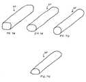
- FIGS. 7A-7Dshow some possible variations of the nano-rod structure formed after an annealing processing in accordance with the present invention.
- Example embodiments of the present inventionwill be described herein in a specific context of making semiconductor devices, such as transistors. In other embodiments not shown, embodiments of the present invention also may include nano-wires or quantum-wires formed in accordance with the present invention. The present invention may also be applied, however, to other situations.
- a preferred manufacturing process in accordance with the present inventionmay be used to make a transistor device. Some of the manufacturing steps of this preferred embodiment being used to make a transistor embodiment are illustrated in FIGS. 1A-6B . While describing the structure formation steps shown in FIGS. 1A-6B , process parameters and steps for the preferred embodiment will described, as well as some of the possible alternatives or variations of the process parameters and steps. However, the process parameters shown and/or described herein are merely examples to illustrate and describe the present invention. With the benefit of this disclosure, one of ordinary skill in the art will likely realize other variations and embodiments of the present invention within the scope and spirit of the appended patent claims.
- FIGS. 1A , 2 A, 3 A, 4 A, 5 A, and 6 Ashow simplified perspective views of one transistor device 20 being manufactured on a semiconductor device. Such a semiconductor device will often have millions of these transistors 20 . However, for purposes of illustration and discussion, only one transistor device 20 is shown and the remainder of the semiconductor device is not shown.
- FIGS. 1B , 2 B, 3 B, 4 B, 5 B, and 6 Bare simplified cross-section views of FIGS. 1A , 2 A, 3 A, 4 A, 5 A, and 6 A, respectively, as taken along lines 1 B— 1 B, 2 B— 2 B, 3 B— 3 B, 4 B— 4 B, 5 B— 5 B, and 6 B— 6 B, respectively.
- an intermediate structureis shown having an insulating layer 22 formed on an underlying layer 24 .
- a semiconductor layer 26is formed on the insulating layer 22 .
- This type of structureis sometimes referred to as a silicon-on-insulator substrate and is commonly available as a starting material.
- a patterned active region mask 28is formed on the semiconductor layer 26 .
- the mask 28may be formed from a pad silicon oxide layer 30 and a silicon nitride layer 32 , for example. With the mask 28 in place having a pattern desired to be formed in the semiconductor layer 26 , the semiconductor layer 26 is preferably anisotropically etched (e.g., dry plasma etching) to conform the semiconductor layer 26 to the pattern of the mask 28 .
- the underlying layer 24will often be a silicon wafer, for example.
- the underlying layer 24may be another type of layer, including but not limited to: an elemental semiconductor, such as germanium; an alloy semiconductor, such as silicon-germanium; or a compound semiconductor, such as gallium arsenide or indium phosphide, for example.
- the insulating layer 22 in some embodimentsmay be referred to as a “buried oxide” layer.
- the insulating layer 22may be composed of a material or a combination of materials from a large variety of materials, including but not limited to: silicon dioxide, silicon nitride, aluminum oxide, plastic, or polymer, for example.
- the insulating layer 22is composed of silicon dioxide (SiO 2 ).
- the semiconductor layer 26may be composed of a material or a combination of materials from a large variety of materials, including but not limited to: any semiconductor material, silicon, carbon, elemental semiconductor material (e.g., germanium), alloy semiconductor material (e.g., silicon-germanium, silicon-germanium-carbon), compound semiconductor material (e.g., indium phosphide, gallium arsenide), plastic, or polymer, for example. Such materials may be in crystalline or amorphous forms.
- the semiconductor layer 26is composed of silicon.
- the semiconductor layer 26is a silicon layer.
- the mask 28has been removed and the patterned semiconductor layer 26 remains in the form of an H-shaped, thin silicon island.
- the patterned semiconductor layer 26may have other shapes (e.g., U-shaped, V-shaped, I-shaped, L-shaped, etc.).
- the thickness of the patterned silicon layer or island 26may range from about two angstroms to about 1000 angstroms, for example.
- the patterned silicon layer 26has a source region 40 , a drain region 42 , and a channel region 44 .
- the channel region 44extends between the source region 40 and the drain region 42 . As shown in FIG. 2A , the channel region 44 has a width that is much narrower than the contact pad portions 50 and 52 of the source and drain regions 40 and 42 , respectively.
- the silicon atoms in the patterned silicon layer 26are re-arranged by annealing the silicon layer 26 at elevated temperatures.
- the re-arrangementis induced by surface migration of silicon atoms driven by a tendency to minimize surface tension.
- the re-arrangement of the atoms at the narrow channel region 44causes the corners of the channel region 44 to be rounded, as shown in FIGS. 3A and 3B , to transform the channel region 44 into a nano-rod structure 60 . If carried out long enough and/or under sufficient heat, the resulting nano-rod structure 60 may be completely rounded having a circular-shaped cross-section, as shown in FIG. 3 B.
- the contact pad portions 50 and 52 of the source and drain regions 40 and 42will also likely experience slight shape changes, such as rounding of at least some of their corners. But because the contact pad portions 50 and 52 are much wider than the channel region, these contact pad portions 50 and 52 will typically still be substantially flat in shape or with only a slight curvature.
- the contact pad portions of the source and drain regionsserve to provide a portion onto which metallic or conductive materials form electrical connection with the source and drain regions. It is understood that the contact pad is an optional feature of this invention. If the contact pad portions of the source and drain regions are omitted, the patterned semiconductor layer may be I-shaped, for example. In this case, the electrical connection between the metallic or conductive material and the source and drain regions may be formed directly on the nano-rod structure.
- the temperature for the annealing processmay range from about 600° C. to about 1200° C.
- the anneal timemay range from about 1 second to about 2 hours.
- the pressure in the reaction chamber (not shown) used for the annealing processmay vary, depending in part upon the environment within the reaction chamber.
- the reaction chambermay be a chemical vapor deposition (CVD) epitaxial reactor, for example.
- the annealing processmay occur in a reaction chamber having an environment of hydrogen gas (H 2 ) at a partial pressure ranging from about 1.0 ⁇ 10 ⁇ 9 torr to about 800 torr.
- the annealing environmentmay be evacuated (i.e., a vacuum environment) at a pressure ranging from about 1.0 ⁇ 10 ⁇ 10 torr to about 1.0 ⁇ 10 ⁇ 3 torr.
- the annealing environmentmay be nitrogen gas (N 2 ) at a pressure ranging from about 1.0 ⁇ 10 ⁇ 9 torr to about 800 torr.
- the annealing environmentmay also be one of the following environments (but not limited to): an environment of a mixed gas including hydrogen and argon; an environment of a mixed gas including hydrogen and nitrogen; an environment with other gases in addition to hydrogen to form a mixed gas ambient; or an environment of an inert gas, for example.
- the annealing processis performed in a hydrogen gas (H 2 ) ambient at about 900° C. for about 2 minutes. During testing, annealing a 28 nm thick silicon channel region 44 under such conditions did not reveal crystal defects.
- H 2hydrogen gas
- the insulating layer 22may be etched to expose the bottom surface of the nano-rod 60 , as shown in FIGS. 4A and 4B .
- the nano-rod 60is supported by the contact portions 50 and 52 of the source and drain regions 40 and 42 . It is preferred to etch away the insulating layer 22 beneath the nano-rod 60 at least enough to allow the gate to wrap around the nano-rod 60 for optimum gate control performance.
- the use of the annealing process of the present invention to form a nano-rod structure 60may also be applied to a non-wrap-around gate design (i.e., where the gate electrode only covers three sides of the gate channel, or where the gate electrode does not completely wrap around the gate channel).
- a gate dielectric material 62is formed on the surface of and about the nano-rod structure 60 (as well as on the other exposed portions of the silicon layer 26 ), as shown in FIGS. 5A and 5B .
- the gate dielectric material 62may be formed completely around the nano-rod surface.
- the gate dielectric material 62may be an oxide formed by thermal oxidation or atomic-layer CVD for uniform deposition, for example. Hence, the gate dielectric will likely form on all exposed areas, including the contact portions 50 , 52 of the source and drain regions 40 , 42 .
- the gate dielectric materialmay take the form of a variety of compositions, including but not limited to: silicon dioxide (SiO 2 ), silicon oxynitride (SiO x N y ), HfO 2 , ZrO 2 , Al 2 O 3 , La 2 O 3 , or other high permittivity materials, for example.
- the gate electrode materialis then deposited, masked, and etched to form the gate electrode 64 , as shown in FIGS. 6A and 6B .
- the gate electrode materialmay be selected from a variety of materials, including but not limited to: a semiconductor material (e.g., poly-silicon, poly-silicon-germanium); a metal material (e.g., molybdenum, tungsten, titanium); a metallic nitride (e.g., tantalum nitride, titanium nitride); or any combination thereof, for example.
- a semiconductor materiale.g., poly-silicon, poly-silicon-germanium
- a metal materiale.g., molybdenum, tungsten, titanium
- a metallic nitridee.g., tantalum nitride, titanium nitride
- the gate electrode 64may be formed completely around the nano-rod 60 , as preferred.
- the gate dielectric material 62may be removed from the source and drain regions, as shown in FIG. 6 A.
- the gate dielectric 62is preferably aligned with the gate electrode 64 at the channel, the gate dielectric 62 can be self-aligned with the gate electrode 64 by simply etching the gate electrode material with an etch chemistry that will also etch away the gate dielectric material 62 while being selective against etching the silicon layer 26 . Also, because the gate dielectric 62 at the gate channel is shielded by the gate electrode 64 , the ion implantation processes for doping the silicon layer 26 outside of the channel (i.e., to form the source and drain of the transistor 20 ) may be self-aligning as well.
- the resulting shape of the nano-rod 60 formed at the channel region 44may vary, depending on the annealing parameters used.
- the nano-rod portion 60 shown in FIG. 7Ahas a generally rectangular shaped cross-section with rounded corners (i.e., more than 4 crystal faces).
- the nano-rod portion 60 shown in FIG. 7Bhas a generally oval-shaped cross-section.
- the nano-rod cross-sectionmay have a rounded but arbitrarily shaped or somewhat arbitrarily shaped, as shown in FIG. 7C for example.
- the preferred shape of the nano-rod cross-section for a preferred transistor embodimentis circular, as shown in FIG. 7 D.
- the nano-rod 60has a diameter no larger than about 65 nm.
- the diameter of the nano-rod cross-sectionmay be in the order of nanometers (e.g., about 4 nm), and such nano-rods may be used for the channel of a field-effect transistor, for example.
- part of the insulating layer 22may be etched away before the annealing process for rounding the corners of the channel region 44 .
- the gate dielectric material 62may be patterned and etched (to leave a gate dielectric portion around the nano-rod 60 where the gate channel will be formed) before the deposition of the gate electrode material.
- the gate electrode materialmay be etched using a first etch chemistry to form the gate electrode 64 , and then the gate dielectric material 62 may be etched using a second etch chemistry after forming the gate electrode 64 .
- the gate electrode 64may act as a self-aligning mask for the etching of the gate dielectric material 62 to shield the gate dielectric between the gate electrode 64 and the nano-rod 60 .
Landscapes
- Engineering & Computer Science (AREA)
- Chemical & Material Sciences (AREA)
- Nanotechnology (AREA)
- Physics & Mathematics (AREA)
- Mathematical Physics (AREA)
- Theoretical Computer Science (AREA)
- Crystallography & Structural Chemistry (AREA)
- Thin Film Transistor (AREA)
- Insulated Gate Type Field-Effect Transistor (AREA)
Abstract
Description
The present invention relates generally to methods for manufacturing semiconductor devices. In one aspect, the present invention relates to a method of forming a nano-rod structure for a channel of a field effect transistor.
Metal-oxide-semiconductor field effect transistor (MOSFET) technology is currently the dominant semiconductor technology used for manufacturing ultra-large scale integrated (ULSI) circuits. As the gate length of the MOSFET is scaled down into the sub-30 nm regime for improved performance and density, the source and drain increasingly interact with the channel to sometimes gain influence on the channel potential. Hence, a transistor with a short gate length often suffers from problems related to the inability of the gate to substantially control the on/off states of the channel, which is often called short-channel effects.
Increased body doping concentration, reduced gate oxide thickness, and junction depths are some ways to suppress short-channel effects. However, for device scaling well into the sub-30 nm regime, the requirements for body-doping concentration, gate oxide thickness, and source/drain doping profiles become increasingly difficult to meet using conventional device structures based on bulk silicon substrates. Thus, alternative device structures that offer better control of short-channel effects are being considered to enable the continued scaling down of transistor sizes.
A highly scalable device structure that offers superior control of short-channel effects is a wrap-around gate structure for a transistor (a.k.a., surround-gate or gate-all-around transistor structure). A wrap-around gate structure typically has a gate that surrounds or wraps around a channel region. This structure effectively improves the capacitance coupling between the gate and the channel, as compared to conventional bulk silicon substrate transistor structures, double-gate transistor structures, and triple-gate transistor structures. With the wrap-around gate structure, the gate gains significant influence on the channel potential, and therefore improves suppression of short-channel effects. A wrap-around gate structure typically allows the gate length to be scaled down by about 50% more compared to a double-gate structure.
There are several different ways to implement a wrap-around gate transistor structure. For example, the transistor channel may be oriented vertically or horizontally. Many of the existing designs for horizontally oriented channels have a square or rectangular shaped cross-section. When the channel cross-section is rectangular or square, enhanced field effect at the corners of the rectangle may cause that part of the transistor to turn on earlier (i.e., having a lower threshold voltage) than parts of the transistor at the flat sides of the rectangular channel cross-section. This may result in a parasitic off-state leakage. Hence, a cylindrical channel cross-section is preferred over a rectangular channel cross-section.
Current attempts at obtaining a more circular channel cross-section are made by oxidizing the silicon beam forming the channel to round the corners of the rectangular channel cross-section. However, this method requires a large amount of oxidation, and hence a large amount of oxide formation, to convert the rectangular channel cross-section shape to a rounded or circular channel cross-section. Hence, there is a need for a way to manufacture a transistor channel having a rounded or circular cross-section shape without having to form excessive oxide about the channel.
The problems and needs outlined above are addressed by embodiments of the present invention. In accordance with one aspect of the present invention, a method of manufacturing a semiconductor device is provided. This method includes the following steps. A semiconductor layer is patterned to form a source region, a channel region, and a drain region in the semiconductor layer. The channel region extends between the source region and the drain region. Corners of the channel region are rounded by annealing the channel region.
Next, some example annealing parameters that may be used are described. The annealing may occur in a reaction chamber having an environment therein including a gas of hydrogen, nitrogen, a mixed gas including hydrogen and argon, a mixed gas including hydrogen and nitrogen, or an inert gas. The annealing environment may be H2gas at a pressure ranging from about 1.0×10⁻⁹torr to about 800 torr. The annealing environment may be N2gas at a pressure ranging from about 1.0×10⁻⁹torr to about 800 torr. The annealing may occur in a reaction chamber having an evacuated environment. The annealing environment may be a vacuum environment at a pressure ranging from about 1.0×10⁻¹⁰torr to about 1.0×10⁻³torr. The annealing may occur in a reaction chamber having a temperature ranging from about 600° C. to about 1200° C. therein. The annealing occurs at an anneal time ranging from about 1 second to about 2 hours. The annealing may be performed in a hydrogen gas (H2) environment at about 900° C. for about 2 minutes.
In accordance with another aspect of the present invention, a method of manufacturing a semiconductor device is provided. This method includes the following steps. A semiconductor layer is patterned to form a source region, a channel region, and a drain region in the semiconductor layer. The channel region extends between the source region and the drain region. Corners of the channel region are rounded by annealing the channel region. The insulating layer is etched using an etch chemistry selective against etching the semiconductor layer. The etching is performed long enough so that at least a segment of the rounded channel region is suspended above a proximate portion of the insulating layer. A gate dielectric material is formed on a surface of and about the rounded channel region. A gate electrode material is formed on the gate dielectric and about the rounded channel region. The gate electrode material is patterned to form a gate electrode. The gate electrode includes a gate wrap region that wraps around the rounded channel region and a gate contact region extending therefrom.
In accordance with yet another aspect of the present invention, a semiconductor device is provided, which includes an insulating layer, an underlying layer, a layer of semiconductor material, a gate dielectric, and a gate electrode. The insulating layer is over the underlying layer. The layer of semiconductor material is over the insulating layer. The semiconductor layer has a source region, a drain region, and an annealed nano-rod structure extending between the source and drain regions. The gate dielectric is formed on the surface of at least a segment of the nano-rod structure. The gate electrode is formed on the surface of the gate dielectric at the segment. Preferably, the gate dielectric and the gate electrode are both formed completely around the nano-rod structure at the segment. Preferably, the nano-rod structure has a cross-section diameter less than about 65 nm.
In accordance with still another aspect of the present invention, a semiconductor device including a plurality of transistors, is provided. Each of the plurality of transistors includes an annealed semiconductor layer, a gate dielectric surface layer, and a gate electrode. The annealed semiconductor layer has a source region, a drain region, and a channel region formed therein. The channel region extends between the source region and the drain region. The source region has a substantially flat source contact portion. The drain region has a substantially flat drain contact portion. The channel region has a substantially circular cross-section shape. The gate dielectric surface layer wraps around a segment of the channel region. The gate electrode has a gate wrap region that wraps around the segment of the channel region and a gate contact region extending therefrom. The gate dielectric layer is between the segment of the channel region and the gate wrap region of the gate electrode.
For a more complete understanding of the present invention, and the advantages thereof, reference is now made to the following descriptions taken in conjunction with the accompanying drawings, in which:
The use of presently preferred embodiments are discussed in detail below. It should be appreciated, however, that the present invention provides many applicable inventive concepts that can be embodied in a wide variety of specific contexts. The specific embodiments discussed are merely illustrative of specific ways to make and use the invention, and do not limit the scope of the invention.
Example embodiments of the present invention will be described herein in a specific context of making semiconductor devices, such as transistors. In other embodiments not shown, embodiments of the present invention also may include nano-wires or quantum-wires formed in accordance with the present invention. The present invention may also be applied, however, to other situations.
A preferred manufacturing process in accordance with the present invention may be used to make a transistor device. Some of the manufacturing steps of this preferred embodiment being used to make a transistor embodiment are illustrated inFIGS. 1A-6B . While describing the structure formation steps shown inFIGS. 1A-6B , process parameters and steps for the preferred embodiment will described, as well as some of the possible alternatives or variations of the process parameters and steps. However, the process parameters shown and/or described herein are merely examples to illustrate and describe the present invention. With the benefit of this disclosure, one of ordinary skill in the art will likely realize other variations and embodiments of the present invention within the scope and spirit of the appended patent claims.
Referring toFIGS. 1A and 1B , an intermediate structure is shown having an insulatinglayer 22 formed on anunderlying layer 24. Asemiconductor layer 26 is formed on the insulatinglayer 22. This type of structure is sometimes referred to as a silicon-on-insulator substrate and is commonly available as a starting material. A patternedactive region mask 28 is formed on thesemiconductor layer 26. Themask 28 may be formed from a padsilicon oxide layer 30 and asilicon nitride layer 32, for example. With themask 28 in place having a pattern desired to be formed in thesemiconductor layer 26, thesemiconductor layer 26 is preferably anisotropically etched (e.g., dry plasma etching) to conform thesemiconductor layer 26 to the pattern of themask 28.
Theunderlying layer 24 will often be a silicon wafer, for example. However, theunderlying layer 24 may be another type of layer, including but not limited to: an elemental semiconductor, such as germanium; an alloy semiconductor, such as silicon-germanium; or a compound semiconductor, such as gallium arsenide or indium phosphide, for example.
The insulatinglayer 22 in some embodiments may be referred to as a “buried oxide” layer. However, the insulatinglayer 22 may be composed of a material or a combination of materials from a large variety of materials, including but not limited to: silicon dioxide, silicon nitride, aluminum oxide, plastic, or polymer, for example. In a currently preferred embodiment, the insulatinglayer 22 is composed of silicon dioxide (SiO2).
Thesemiconductor layer 26 may be composed of a material or a combination of materials from a large variety of materials, including but not limited to: any semiconductor material, silicon, carbon, elemental semiconductor material (e.g., germanium), alloy semiconductor material (e.g., silicon-germanium, silicon-germanium-carbon), compound semiconductor material (e.g., indium phosphide, gallium arsenide), plastic, or polymer, for example. Such materials may be in crystalline or amorphous forms. In a currently preferred embodiment, thesemiconductor layer 26 is composed of silicon. Hence, in the preferred embodiment shown inFIGS. 1A-6B , thesemiconductor layer 26 is a silicon layer.
InFIGS. 2A and 2B themask 28 has been removed and the patternedsemiconductor layer 26 remains in the form of an H-shaped, thin silicon island. However, in other embodiments (not shown), the patternedsemiconductor layer 26 may have other shapes (e.g., U-shaped, V-shaped, I-shaped, L-shaped, etc.). The thickness of the patterned silicon layer orisland 26 may range from about two angstroms to about 1000 angstroms, for example. The patternedsilicon layer 26 has asource region 40, adrain region 42, and achannel region 44. Thechannel region 44 extends between thesource region 40 and thedrain region 42. As shown inFIG. 2A , thechannel region 44 has a width that is much narrower than thecontact pad portions 50 and52 of the source and drainregions
Next, the silicon atoms in the patternedsilicon layer 26 are re-arranged by annealing thesilicon layer 26 at elevated temperatures. The re-arrangement is induced by surface migration of silicon atoms driven by a tendency to minimize surface tension. During the annealing, the re-arrangement of the atoms at thenarrow channel region 44 causes the corners of thechannel region 44 to be rounded, as shown inFIGS. 3A and 3B , to transform thechannel region 44 into a nano-rod structure 60. If carried out long enough and/or under sufficient heat, the resulting nano-rod structure 60 may be completely rounded having a circular-shaped cross-section, as shown in FIG.3B. Thecontact pad portions 50 and52 of the source and drainregions contact pad portions 50 and52 are much wider than the channel region, thesecontact pad portions 50 and52 will typically still be substantially flat in shape or with only a slight curvature. The contact pad portions of the source and drain regions serve to provide a portion onto which metallic or conductive materials form electrical connection with the source and drain regions. It is understood that the contact pad is an optional feature of this invention. If the contact pad portions of the source and drain regions are omitted, the patterned semiconductor layer may be I-shaped, for example. In this case, the electrical connection between the metallic or conductive material and the source and drain regions may be formed directly on the nano-rod structure.
Example parameters for the annealing process used to round the corners of thechannel region 44 will be described next. The temperature for the annealing process may range from about 600° C. to about 1200° C. The anneal time may range from about 1 second to about 2 hours. The pressure in the reaction chamber (not shown) used for the annealing process may vary, depending in part upon the environment within the reaction chamber. The reaction chamber may be a chemical vapor deposition (CVD) epitaxial reactor, for example. The annealing process may occur in a reaction chamber having an environment of hydrogen gas (H2) at a partial pressure ranging from about 1.0×10⁻⁹torr to about 800 torr. In another embodiment, the annealing environment may be evacuated (i.e., a vacuum environment) at a pressure ranging from about 1.0×10⁻¹⁰torr to about 1.0×10⁻³torr. In still another embodiment, the annealing environment may be nitrogen gas (N2) at a pressure ranging from about 1.0×10⁻⁹torr to about 800 torr. The annealing environment may also be one of the following environments (but not limited to): an environment of a mixed gas including hydrogen and argon; an environment of a mixed gas including hydrogen and nitrogen; an environment with other gases in addition to hydrogen to form a mixed gas ambient; or an environment of an inert gas, for example.
In a preferred embodiment, the annealing process is performed in a hydrogen gas (H2) ambient at about 900° C. for about 2 minutes. During testing, annealing a 28 nm thicksilicon channel region 44 under such conditions did not reveal crystal defects.
After forming the nano-rod structure 60, the insulatinglayer 22 may be etched to expose the bottom surface of the nano-rod 60, as shown inFIGS. 4A and 4B . The nano-rod 60 is supported by thecontact portions 50 and52 of the source and drainregions layer 22 beneath the nano-rod 60 at least enough to allow the gate to wrap around the nano-rod 60 for optimum gate control performance. The use of the annealing process of the present invention to form a nano-rod structure60 (described above) may also be applied to a non-wrap-around gate design (i.e., where the gate electrode only covers three sides of the gate channel, or where the gate electrode does not completely wrap around the gate channel).
Next, agate dielectric material 62 is formed on the surface of and about the nano-rod structure60 (as well as on the other exposed portions of the silicon layer26), as shown inFIGS. 5A and 5B . As shown inFIG. 5B , because the nano-rod 60 is exposed on all sides after etching away part of theinsulting layer 22, thegate dielectric material 62 may be formed completely around the nano-rod surface. Thegate dielectric material 62 may be an oxide formed by thermal oxidation or atomic-layer CVD for uniform deposition, for example. Hence, the gate dielectric will likely form on all exposed areas, including thecontact portions 50,52 of the source and drainregions
A gate electrode material is then deposited, masked, and etched to form thegate electrode 64, as shown inFIGS. 6A and 6B . The gate electrode material may be selected from a variety of materials, including but not limited to: a semiconductor material (e.g., poly-silicon, poly-silicon-germanium); a metal material (e.g., molybdenum, tungsten, titanium); a metallic nitride (e.g., tantalum nitride, titanium nitride); or any combination thereof, for example. As shown inFIG. 6B , because the nano-rod 60 is elevated above the insulating layer22 (at least where the channel will be formed), thegate electrode 64 may be formed completely around the nano-rod 60, as preferred. During or after the etching of the gate electrode material to form the patternedgate electrode 64, thegate dielectric material 62 may be removed from the source and drain regions, as shown in FIG.6A.
Because thegate dielectric 62 is preferably aligned with thegate electrode 64 at the channel, thegate dielectric 62 can be self-aligned with thegate electrode 64 by simply etching the gate electrode material with an etch chemistry that will also etch away thegate dielectric material 62 while being selective against etching thesilicon layer 26. Also, because thegate dielectric 62 at the gate channel is shielded by thegate electrode 64, the ion implantation processes for doping thesilicon layer 26 outside of the channel (i.e., to form the source and drain of the transistor20) may be self-aligning as well.
As shown inFIGS. 7A ,7B,7C, and7D, the resulting shape of the nano-rod 60 formed at thechannel region 44 may vary, depending on the annealing parameters used. For example, the nano-rod portion 60 shown inFIG. 7A has a generally rectangular shaped cross-section with rounded corners (i.e., more than 4 crystal faces). The nano-rod portion 60 shown inFIG. 7B has a generally oval-shaped cross-section. In other embodiments, the nano-rod cross-section may have a rounded but arbitrarily shaped or somewhat arbitrarily shaped, as shown inFIG. 7C for example. However, as described above, the preferred shape of the nano-rod cross-section for a preferred transistor embodiment is circular, as shown in FIG.7D. Preferably, the nano-rod 60 has a diameter no larger than about 65 nm. The diameter of the nano-rod cross-section may be in the order of nanometers (e.g., about 4 nm), and such nano-rods may be used for the channel of a field-effect transistor, for example.
In another manufacturing embodiment (not shown) of present invention, afterFIG. 2A , part of the insulatinglayer 22 may be etched away before the annealing process for rounding the corners of thechannel region 44. Also, afterFIG. 5A , thegate dielectric material 62 may be patterned and etched (to leave a gate dielectric portion around the nano-rod 60 where the gate channel will be formed) before the deposition of the gate electrode material. In still another embodiment, afterFIG. 5A , the gate electrode material may be etched using a first etch chemistry to form thegate electrode 64, and then thegate dielectric material 62 may be etched using a second etch chemistry after forming thegate electrode 64. In such case, thegate electrode 64 may act as a self-aligning mask for the etching of thegate dielectric material 62 to shield the gate dielectric between thegate electrode 64 and the nano-rod 60.
Although several embodiments of the present invention have been described in detail, it should be understood that various changes, substitutions and alterations can be made herein without departing from the spirit and scope of the invention as defined by the appended claims. Moreover, the scope of the present application is not intended to be limited to the particular embodiments of the processes, machines, manufactures, compositions of matter, means, methods and steps described in the specification. As one of ordinary skill in the art will readily appreciate from the disclosure of the present invention, processes, machines, manufactures, compositions of matter, means, methods, or steps, presently existing or later to be developed, that perform substantially the same function and/or achieve substantially the same result as the corresponding embodiments described herein may be utilized according to the present invention. Accordingly, the appended claims are intended to include within their scope such processes, machines, manufactures, compositions of matter, means, methods, or steps.
Claims (12)
1. A method of manufacturing a semiconductor device, comprising:
providing a semiconductor structure comprising a semiconductor layer overlying an insulating material;
patterning the semiconductor layer to form a source region, a channel region, and a drain region in the semiconductor layer, wherein the channel region extends between the source region and the drain region; and
rounding corners of the channel region by annealing.
2. The method ofclaim 1 , wherein the annealing occurs in a reaction chamber having an environment therein including a gas selected from a group consisting of hydrogen, nitrogen, a mixed gas including hydrogen and argon, a mixed gas including hydrogen and nitrogen, and an inert gas.
3. The method ofclaim 2 , wherein the annealing environment is H2gas at a pressure ranging from about 1.0×10⁻⁹torr to about 800 torr.
4. The method ofclaim 2 , wherein the annealing environment is N2gas at a pressure ranging from about 1.0×10⁻⁹torr to about 800 torr.
5. The method ofclaim 1 , wherein the annealing occurs in a reaction chamber having an evacuated environment.
6. The method ofclaim 5 , wherein the annealing environment is a vacuum environment at a pressure ranging from about 1.0×10⁻¹⁰torr to about 1.0×10⁻³torr.
7. The method ofclaim 1 , wherein the annealing occurs in a reaction chamber having a temperature ranging from about 600° C. to about 1200° C. therein.
8. The method ofclaim 1 , wherein the annealing occurs at an anneal time ranging from about 1 second to about 2 hours.
9. The method ofclaim 1 , wherein the annealing is performed in a hydrogen gas (H2) environment at about 900° C. for about 2 minutes.
10. The method ofclaim 1 , further comprising:
etching the insulating layer using an etch chemistry selective against etching the semiconductor layer, wherein the etching is performed long enough so that at least a segment of the channel region is suspended above a proximate portion of the insulating layer;
forming a gate dielectric material on a surface of and about the rounded channel region;
forming a gate electrode material on the gate dielectric and about the rounded channel region; and
patterning the gate electrode material to form a gate electrode, the gate electrode comprising a gate wrap region that wraps around the rounded channel region and a gate contact region extending therefrom.
11. The method ofclaim 1 , further comprising:
doping exposed portions of the semiconductor layer.
12. A method of manufacturing a semiconductor nano-rod device, comprising:
patterning a semiconductor layer to form a source region, a channel region, and a drain region in the semiconductor layer, wherein the channel region extends between the source region and the drain region;
rounding corners of the channel region by annealing the channel region;
etching the insulating layer using an etch chemistry selective against etching the semiconductor layer, wherein the etching is performed long enough so that at least a segment of the rounded channel region is suspended above a proximate portion of the insulating layer;
forming a gate dielectric material on a surface of and about the rounded channel region;
forming a gate electrode material on the gate dielectric and about the rounded channel region; and
patterning the gate electrode material to form a gate electrode, the gate electrode comprising a gate wrap region that wraps around the rounded channel region and a gate contact region extending therefrom.
Priority Applications (3)
| Application Number | Priority Date | Filing Date | Title |
|---|---|---|---|
| US10/370,792US6855606B2 (en) | 2003-02-20 | 2003-02-20 | Semiconductor nano-rod devices |
| TW092122206ATWI222222B (en) | 2003-02-20 | 2003-08-13 | Method for forming rod-shaped semiconductor layer, and rod-shaped semiconductor device and method of fabricating the same |
| US11/031,703US20050121706A1 (en) | 2003-02-20 | 2005-01-07 | Semiconductor nano-rod devices |
Applications Claiming Priority (1)
| Application Number | Priority Date | Filing Date | Title |
|---|---|---|---|
| US10/370,792US6855606B2 (en) | 2003-02-20 | 2003-02-20 | Semiconductor nano-rod devices |
Related Child Applications (1)
| Application Number | Title | Priority Date | Filing Date |
|---|---|---|---|
| US11/031,703DivisionUS20050121706A1 (en) | 2003-02-20 | 2005-01-07 | Semiconductor nano-rod devices |
Publications (2)
| Publication Number | Publication Date |
|---|---|
| US20040166642A1 US20040166642A1 (en) | 2004-08-26 |
| US6855606B2true US6855606B2 (en) | 2005-02-15 |
Family
ID=32868227
Family Applications (2)
| Application Number | Title | Priority Date | Filing Date |
|---|---|---|---|
| US10/370,792Expired - LifetimeUS6855606B2 (en) | 2003-02-20 | 2003-02-20 | Semiconductor nano-rod devices |
| US11/031,703AbandonedUS20050121706A1 (en) | 2003-02-20 | 2005-01-07 | Semiconductor nano-rod devices |
Family Applications After (1)
| Application Number | Title | Priority Date | Filing Date |
|---|---|---|---|
| US11/031,703AbandonedUS20050121706A1 (en) | 2003-02-20 | 2005-01-07 | Semiconductor nano-rod devices |
Country Status (2)
| Country | Link |
|---|---|
| US (2) | US6855606B2 (en) |
| TW (1) | TWI222222B (en) |
Cited By (69)
| Publication number | Priority date | Publication date | Assignee | Title |
|---|---|---|---|---|
| US20050156171A1 (en)* | 2003-12-30 | 2005-07-21 | Brask Justin K. | Nonplanar transistors with metal gate electrodes |
| US20050266692A1 (en)* | 2004-06-01 | 2005-12-01 | Brask Justin K | Method of patterning a film |
| US20050275010A1 (en)* | 2004-06-10 | 2005-12-15 | Hung-Wei Chen | Semiconductor nano-wire devices and methods of fabrication |
| US20060068591A1 (en)* | 2004-09-29 | 2006-03-30 | Marko Radosavljevic | Fabrication of channel wraparound gate structure for field-effect transistor |
| US20060086977A1 (en)* | 2004-10-25 | 2006-04-27 | Uday Shah | Nonplanar device with thinned lower body portion and method of fabrication |
| US20060172497A1 (en)* | 2003-06-27 | 2006-08-03 | Hareland Scott A | Nonplanar semiconductor device with partially or fully wrapped around gate electrode and methods of fabrication |
| US20060186484A1 (en)* | 2005-02-23 | 2006-08-24 | Chau Robert S | Field effect transistor with narrow bandgap source and drain regions and method of fabrication |
| US20060202266A1 (en)* | 2005-03-14 | 2006-09-14 | Marko Radosavljevic | Field effect transistor with metal source/drain regions |
| US20060216897A1 (en)* | 2005-03-24 | 2006-09-28 | Samsung Electronics Co., Ltd. | Semiconductor device having a round-shaped nano-wire transistor channel and method of manufacturing same |
| US20060220133A1 (en)* | 2003-04-29 | 2006-10-05 | Yee-Chia Yeo | Doping of semiconductor fin devices |
| US20060261411A1 (en)* | 2003-06-27 | 2006-11-23 | Hareland Scott A | Nonplanar device with stress incorporation layer and method of fabrication |
| US20070001173A1 (en)* | 2005-06-21 | 2007-01-04 | Brask Justin K | Semiconductor device structures and methods of forming semiconductor structures |
| US20070026615A1 (en)* | 2005-07-27 | 2007-02-01 | Sinan Goktepeli | Method of forming a FINFET structure |
| US20070090408A1 (en)* | 2005-09-29 | 2007-04-26 | Amlan Majumdar | Narrow-body multiple-gate FET with dominant body transistor for high performance |
| US20070111419A1 (en)* | 2005-09-28 | 2007-05-17 | Doyle Brian S | CMOS Devices with a single work function gate electrode and method of fabrication |
| US20070148837A1 (en)* | 2005-12-27 | 2007-06-28 | Uday Shah | Method of fabricating a multi-cornered film |
| US20070158679A1 (en)* | 2005-12-31 | 2007-07-12 | Samsung Electronics Co., Ltd. | Semiconductor device with multiple channels and method of fabricating the same |
| US20070262389A1 (en)* | 2004-01-16 | 2007-11-15 | Robert Chau | Tri-gate transistors and methods to fabricate same |
| KR100801063B1 (en) | 2006-10-02 | 2008-02-04 | 삼성전자주식회사 | Gate all around type semiconductor device and manufacturing method thereof |
| US7361958B2 (en) | 2004-09-30 | 2008-04-22 | Intel Corporation | Nonplanar transistors with metal gate electrodes |
| US20080142841A1 (en)* | 2004-03-31 | 2008-06-19 | Nick Lindert | Bulk non-planar transistor having strained enhanced mobility and methods of fabrication |
| US20080157225A1 (en)* | 2006-12-29 | 2008-07-03 | Suman Datta | SRAM and logic transistors with variable height multi-gate transistor architecture |
| US20080188041A1 (en)* | 2005-08-17 | 2008-08-07 | Suman Datta | Lateral undercut of metal gate in SOI device |
| US20080258207A1 (en)* | 2005-06-30 | 2008-10-23 | Marko Radosavljevic | Block Contact Architectures for Nanoscale Channel Transistors |
| US20080296557A1 (en)* | 2004-01-22 | 2008-12-04 | Franz Kreupl | Semiconductor Power Switch and Method for Producing a Semiconductor Power Switch |
| WO2008121383A3 (en)* | 2007-03-29 | 2008-12-11 | Northrop Grumman Systems Corp | Curled semiconductor transistor |
| US7479421B2 (en) | 2005-09-28 | 2009-01-20 | Intel Corporation | Process for integrating planar and non-planar CMOS transistors on a bulk substrate and article made thereby |
| US20090114904A1 (en)* | 2005-06-08 | 2009-05-07 | Samsung Electronics Co., Ltd. | Semiconductor devices having nano-line channels |
| US20090209071A1 (en)* | 2008-02-18 | 2009-08-20 | Samsung Elecronics Co., Ltd. | Methods of manufacturing semiconductor devices |
| US20090242964A1 (en)* | 2006-04-26 | 2009-10-01 | Nxp B.V. | Non-volatile memory device |
| US20100065888A1 (en)* | 2004-06-30 | 2010-03-18 | Shaheen Mohamad A | High mobility tri-gate devices and methods of fabrication |
| US20100081227A1 (en)* | 2007-07-03 | 2010-04-01 | Hong Kl-Ha | Luminous device and method of manufacturing the same |
| US20100090197A1 (en)* | 2008-10-10 | 2010-04-15 | Electonics And Telecommunications Research Institute | Method of manufacturing semiconductor nanowire sensor device and semiconductor nanowire sensor device manufactured according to the method |
| US20100204062A1 (en)* | 2008-11-07 | 2010-08-12 | University Of Southern California | Calibration methods for multiplexed sensor arrays |
| US20100256344A1 (en)* | 2009-04-03 | 2010-10-07 | University Of Southern California | Surface modification of nanosensor platforms to increase sensitivity and reproducibility |
| US20100255680A1 (en)* | 2009-04-03 | 2010-10-07 | International Business Machines Corporation | Top-Down Nanowire Thinning Processes |
| US20100260745A1 (en)* | 2007-10-01 | 2010-10-14 | University Of Southern California | Methods of using and constructing nanosensor platforms |
| US20100297838A1 (en)* | 2004-09-29 | 2010-11-25 | Chang Peter L D | Independently accessed double-gate and tri-gate transistors in same process flow |
| US20100295021A1 (en)* | 2009-05-21 | 2010-11-25 | International Business Machines Corporation | Single Gate Inverter Nanowire Mesh |
| US20110012090A1 (en)* | 2007-12-07 | 2011-01-20 | Agency For Science, Technology And Research | Silicon-germanium nanowire structure and a method of forming the same |
| US20110018065A1 (en)* | 2008-02-26 | 2011-01-27 | Nxp B.V. | Method for manufacturing semiconductor device and semiconductor device |
| US20110062520A1 (en)* | 2005-06-15 | 2011-03-17 | Brask Justin K | Method for fabricating transistor with thinned channel |
| US20110133161A1 (en)* | 2009-12-04 | 2011-06-09 | International Business Machines Corporation | Omega Shaped Nanowire Tunnel Field Effect Transistors |
| US20110133162A1 (en)* | 2009-12-04 | 2011-06-09 | International Business Machines Corporation | Gate-All-Around Nanowire Field Effect Transistors |
| US20110133164A1 (en)* | 2009-12-04 | 2011-06-09 | International Business Machines Corporation | Omega Shaped Nanowire Field Effect Transistors |
| US20110133165A1 (en)* | 2009-12-04 | 2011-06-09 | International Business Machines Corporation | Self-aligned contacts for nanowire field effect transistors |
| US20110136279A1 (en)* | 2005-03-17 | 2011-06-09 | Samsung Electronics Co., Ltd. | Thin film transistor, thin film transistor display panel, and manufacturing method thereof |
| US20110133169A1 (en)* | 2009-12-04 | 2011-06-09 | International Business Machines Corporation | Gate-All-Around Nanowire Tunnel Field Effect Transistors |
| US20110133167A1 (en)* | 2009-12-04 | 2011-06-09 | International Business Machines Corporation | Planar and nanowire field effect transistors |
| US7960794B2 (en) | 2004-08-10 | 2011-06-14 | Intel Corporation | Non-planar pMOS structure with a strained channel region and an integrated strained CMOS flow |
| US20110168982A1 (en)* | 2010-01-08 | 2011-07-14 | International Business Machines Corporation | Nanowire pin tunnel field effect devices |
| US7989280B2 (en) | 2005-11-30 | 2011-08-02 | Intel Corporation | Dielectric interface for group III-V semiconductor device |
| KR101054345B1 (en)* | 2005-04-14 | 2011-08-04 | 삼성전자주식회사 | Transistor, display device including same and manufacturing method thereof |
| CN102208351A (en)* | 2011-05-27 | 2011-10-05 | 北京大学 | Preparation method of fence silicon nanowire transistor of air side wall |
| CN102214595A (en)* | 2011-05-26 | 2011-10-12 | 北京大学 | Manufacturing method of fence silicon nanowire transistor with air as side wall |
| CN102214611A (en)* | 2011-05-27 | 2011-10-12 | 北京大学 | Preparation method for gate-all-round silicon nanowire transistor by using air as side wall |
| CN102214596A (en)* | 2011-05-26 | 2011-10-12 | 北京大学 | Manufacturing method of fence silicon nanowire transistor with air as side wall |
| US20120007051A1 (en)* | 2010-07-06 | 2012-01-12 | International Business Machines Corporation | Process for Forming a Surrounding Gate for a Nanowire Using a Sacrificial Patternable Dielectric |
| WO2012159424A1 (en)* | 2011-05-26 | 2012-11-29 | 北京大学 | Wet etching-based method for producing silicon nanowire field effect transistor |
| US8324940B2 (en) | 2010-04-13 | 2012-12-04 | International Business Machines Corporation | Nanowire circuits in matched devices |
| US8324030B2 (en) | 2010-05-12 | 2012-12-04 | International Business Machines Corporation | Nanowire tunnel field effect transistors |
| US8361907B2 (en) | 2010-05-10 | 2013-01-29 | International Business Machines Corporation | Directionally etched nanowire field effect transistors |
| US8362566B2 (en) | 2008-06-23 | 2013-01-29 | Intel Corporation | Stress in trigate devices using complimentary gate fill materials |
| US8513068B2 (en) | 2010-09-17 | 2013-08-20 | International Business Machines Corporation | Nanowire field effect transistors |
| US8586966B2 (en) | 2010-08-16 | 2013-11-19 | International Business Machines Corporation | Contacts for nanowire field effect transistors |
| US8617945B2 (en) | 2006-08-02 | 2013-12-31 | Intel Corporation | Stacking fault and twin blocking barrier for integrating III-V on Si |
| US8735869B2 (en)* | 2012-09-27 | 2014-05-27 | Intel Corporation | Strained gate-all-around semiconductor devices formed on globally or locally isolated substrates |
| US20140299835A1 (en)* | 2011-10-04 | 2014-10-09 | Centre National De La Recherche Scientifique | Ram memory point with a transistor |
| US11594608B2 (en) | 2019-04-19 | 2023-02-28 | Institute of Microelectronics, Chinese Academy of Sciences | Method for forming gate-all-around nanowire device |
Families Citing this family (94)
| Publication number | Priority date | Publication date | Assignee | Title |
|---|---|---|---|---|
| JP4123961B2 (en)* | 2002-03-26 | 2008-07-23 | 富士電機デバイステクノロジー株式会社 | Manufacturing method of semiconductor device |
| US20050106794A1 (en)* | 2002-03-26 | 2005-05-19 | Fuji Electric Holdings Co., Ltd. | Method of manufacturing a semiconductor device |
| US7358121B2 (en)* | 2002-08-23 | 2008-04-15 | Intel Corporation | Tri-gate devices and methods of fabrication |
| US7624192B2 (en)* | 2003-12-30 | 2009-11-24 | Microsoft Corporation | Framework for user interaction with multiple network devices |
| US7193279B2 (en)* | 2005-01-18 | 2007-03-20 | Intel Corporation | Non-planar MOS structure with a strained channel region |
| FR2884648B1 (en)* | 2005-04-13 | 2007-09-07 | Commissariat Energie Atomique | STRUCTURE AND METHOD FOR PRODUCING A MICROELECTRONIC DEVICE HAVING ONE OR MORE QUANTUM THREADS FOR FORMING A CHANNEL OR MORE CHANNELS OF TRANSISTORS |
| US7541227B2 (en)* | 2005-06-02 | 2009-06-02 | Hewlett-Packard Development Company, L.P. | Thin film devices and methods for forming the same |
| US7709054B2 (en)* | 2005-07-19 | 2010-05-04 | Wayne State University | Particle-rod nano structures and method of forming same by spin coating |
| FR2889622A1 (en)* | 2005-08-08 | 2007-02-09 | St Microelectronics Crolles 2 | PROCESS FOR MANUFACTURING A PARALLEL SEMICONDUCTOR NANODOIGT TRANSISTOR |
| US7485908B2 (en)* | 2005-08-18 | 2009-02-03 | United States Of America As Represented By The Secretary Of The Air Force | Insulated gate silicon nanowire transistor and method of manufacture |
| US7803668B2 (en)* | 2006-02-24 | 2010-09-28 | Stmicroelectronics (Crolles 2) Sas | Transistor and fabrication process |
| US7449373B2 (en)* | 2006-03-31 | 2008-11-11 | Intel Corporation | Method of ion implanting for tri-gate devices |
| FR2900765B1 (en)* | 2006-05-04 | 2008-10-10 | Commissariat Energie Atomique | METHOD OF MAKING A TRANSISTOR GRID COMPRISING A DECOMPOSITION OF PRECURSOR MATERIAL IN AT LEAST ONE METALLIC MATERIAL USING AT LEAST ONE ELECTRON BEAM |
| US7667260B2 (en)* | 2006-08-09 | 2010-02-23 | Micron Technology, Inc. | Nanoscale floating gate and methods of formation |
| FR2905197B1 (en)* | 2006-08-25 | 2008-12-19 | Commissariat Energie Atomique | METHOD FOR PRODUCING A DEVICE COMPRISING A STRUCTURE PROVIDED WITH ONE OR MORE MICROWIRES OR NANO-THREADS BASED ON A COMPOUND OF SI AND GE, BY GERMANIUM CONDENSATION |
| KR100757328B1 (en)* | 2006-10-04 | 2007-09-11 | 삼성전자주식회사 | Monoelectron transistor and method of manufacturing the same |
| US7935599B2 (en)* | 2007-04-04 | 2011-05-03 | Sharp Laboratories Of America, Inc. | Nanowire transistor and method for forming same |
| KR101375833B1 (en)* | 2007-05-03 | 2014-03-18 | 삼성전자주식회사 | Field effect transistor having germanium nanorod and method of manufacturing the same |
| US7781825B2 (en)* | 2007-10-18 | 2010-08-24 | Macronix International Co., Ltd. | Semiconductor device and method for manufacturing the same |
| KR101406224B1 (en)* | 2007-10-26 | 2014-06-12 | 삼성전자주식회사 | Nanowire transistor and method of manufacturing the same |
| FR2923646A1 (en)* | 2007-11-09 | 2009-05-15 | Commissariat Energie Atomique | MEMORY CELL SRAM WITH TRANSISTORS WITH VERTICAL MULTI-CHANNEL STRUCTURE |
| FR2923652B1 (en)* | 2007-11-09 | 2010-06-11 | Commissariat Energie Atomique | METHOD FOR MANUFACTURING PARALLEL NANOWILS WITH THEIR SUPPORT SUBSTRATE |
| US8999851B2 (en)* | 2007-12-14 | 2015-04-07 | Oned Material Llc | Methods for formation of substrate elements |
| EP2073256A1 (en)* | 2007-12-20 | 2009-06-24 | Interuniversitair Microelektronica Centrum vzw ( IMEC) | Method for fabricating a semiconductor device and the semiconductor device made thereof |
| US8022393B2 (en) | 2008-07-29 | 2011-09-20 | Nokia Corporation | Lithographic process using a nanowire mask, and nanoscale devices fabricated using the process |
| US7884004B2 (en)* | 2009-02-04 | 2011-02-08 | International Business Machines Corporation | Maskless process for suspending and thinning nanowires |
| US8080456B2 (en)* | 2009-05-20 | 2011-12-20 | International Business Machines Corporation | Robust top-down silicon nanowire structure using a conformal nitride |
| US8519479B2 (en)* | 2010-05-12 | 2013-08-27 | International Business Machines Corporation | Generation of multiple diameter nanowire field effect transistors |
| US8420455B2 (en)* | 2010-05-12 | 2013-04-16 | International Business Machines Corporation | Generation of multiple diameter nanowire field effect transistors |
| TWI406423B (en)* | 2010-06-08 | 2013-08-21 | Nat Univ Tsing Hua | Columnar diamond Xiaoji diode and manufacturing method thereof |
| CN102290447B (en)* | 2010-06-18 | 2013-06-05 | 国立清华大学 | Pillar diamond Schottky diode and method of making same |
| US8680510B2 (en)* | 2010-06-28 | 2014-03-25 | International Business Machines Corporation | Method of forming compound semiconductor |
| CN102074577B (en) | 2010-10-09 | 2013-03-06 | 北京大学 | Vertical channel field effect transistor and preparation method thereof |
| CN102280454B (en)* | 2011-08-22 | 2013-02-06 | 中国科学院半导体研究所 | Semiconductor transistor structure and manufacturing method thereof |
| US8852998B1 (en)* | 2011-08-30 | 2014-10-07 | Sandia Corporation | Method to fabricate micro and nano diamond devices |
| US9087863B2 (en)* | 2011-12-23 | 2015-07-21 | Intel Corporation | Nanowire structures having non-discrete source and drain regions |
| US8901659B2 (en)* | 2012-02-09 | 2014-12-02 | International Business Machines Corporation | Tapered nanowire structure with reduced off current |
| US9501738B1 (en)* | 2012-08-16 | 2016-11-22 | Sandia Corporation | Cellular computational platform and neurally inspired elements thereof |
| CN103824775B (en)* | 2012-11-16 | 2018-04-24 | 中国科学院微电子研究所 | FinFET and manufacturing method thereof |
| US8927405B2 (en)* | 2012-12-18 | 2015-01-06 | International Business Machines Corporation | Accurate control of distance between suspended semiconductor nanowires and substrate surface |
| US9224849B2 (en)* | 2012-12-28 | 2015-12-29 | Taiwan Semiconductor Manufacturing Company, Ltd. | Transistors with wrapped-around gates and methods for forming the same |
| US8927397B2 (en)* | 2013-02-07 | 2015-01-06 | International Business Machines Corporation | Diode structure and method for gate all around silicon nanowire technologies |
| US9583414B2 (en) | 2013-10-31 | 2017-02-28 | Qorvo Us, Inc. | Silicon-on-plastic semiconductor device and method of making the same |
| US9214337B2 (en) | 2013-03-06 | 2015-12-15 | Rf Micro Devices, Inc. | Patterned silicon-on-plastic (SOP) technology and methods of manufacturing the same |
| US9812350B2 (en) | 2013-03-06 | 2017-11-07 | Qorvo Us, Inc. | Method of manufacture for a silicon-on-plastic semiconductor device with interfacial adhesion layer |
| US9006842B2 (en) | 2013-05-30 | 2015-04-14 | Taiwan Semiconductor Manufacturing Company, Ltd. | Tuning strain in semiconductor devices |
| US9349850B2 (en) | 2013-07-17 | 2016-05-24 | Taiwan Semiconductor Manufacturing Company, Ltd. | Thermally tuning strain in semiconductor devices |
| US10553718B2 (en)* | 2014-03-14 | 2020-02-04 | Taiwan Semiconductor Manufacturing Co., Ltd. | Semiconductor devices with core-shell structures |
| US9698261B2 (en)* | 2014-06-30 | 2017-07-04 | Taiwan Semiconductor Manufacturing Co., Ltd. | Vertical device architecture |
| TWI582847B (en) | 2014-09-12 | 2017-05-11 | Rf微型儀器公司 | Printed circuit module having semiconductor device with a polymer substrate and methods of manufacturing the same |
| US10085352B2 (en) | 2014-10-01 | 2018-09-25 | Qorvo Us, Inc. | Method for manufacturing an integrated circuit package |
| US9530709B2 (en) | 2014-11-03 | 2016-12-27 | Qorvo Us, Inc. | Methods of manufacturing a printed circuit module having a semiconductor device with a protective layer in place of a low-resistivity handle layer |
| WO2016105408A1 (en)* | 2014-12-24 | 2016-06-30 | Intel Corporation | Field effect transistor structures using germanium nanowires |
| CN106033725B (en) | 2015-03-13 | 2020-10-16 | 联华电子股份有限公司 | Semiconductor element and manufacturing process thereof |
| US9613831B2 (en) | 2015-03-25 | 2017-04-04 | Qorvo Us, Inc. | Encapsulated dies with enhanced thermal performance |
| US9960145B2 (en) | 2015-03-25 | 2018-05-01 | Qorvo Us, Inc. | Flip chip module with enhanced properties |
| US20160343604A1 (en) | 2015-05-22 | 2016-11-24 | Rf Micro Devices, Inc. | Substrate structure with embedded layer for post-processing silicon handle elimination |
| US10276495B2 (en) | 2015-09-11 | 2019-04-30 | Qorvo Us, Inc. | Backside semiconductor die trimming |
| US10020405B2 (en) | 2016-01-19 | 2018-07-10 | Qorvo Us, Inc. | Microelectronics package with integrated sensors |
| US10062583B2 (en) | 2016-05-09 | 2018-08-28 | Qorvo Us, Inc. | Microelectronics package with inductive element and magnetically enhanced mold compound component |
| US10468329B2 (en) | 2016-07-18 | 2019-11-05 | Qorvo Us, Inc. | Thermally enhanced semiconductor package having field effect transistors with back-gate feature |
| US10784149B2 (en) | 2016-05-20 | 2020-09-22 | Qorvo Us, Inc. | Air-cavity module with enhanced device isolation |
| US10773952B2 (en) | 2016-05-20 | 2020-09-15 | Qorvo Us, Inc. | Wafer-level package with enhanced performance |
| US10103080B2 (en) | 2016-06-10 | 2018-10-16 | Qorvo Us, Inc. | Thermally enhanced semiconductor package with thermal additive and process for making the same |
| US10109550B2 (en) | 2016-08-12 | 2018-10-23 | Qorvo Us, Inc. | Wafer-level package with enhanced performance |
| SG11201901193UA (en) | 2016-08-12 | 2019-03-28 | Qorvo Us Inc | Wafer-level package with enhanced performance |
| US10486965B2 (en) | 2016-08-12 | 2019-11-26 | Qorvo Us, Inc. | Wafer-level package with enhanced performance |
| US10109502B2 (en) | 2016-09-12 | 2018-10-23 | Qorvo Us, Inc. | Semiconductor package with reduced parasitic coupling effects and process for making the same |
| US10090339B2 (en) | 2016-10-21 | 2018-10-02 | Qorvo Us, Inc. | Radio frequency (RF) switch |
| US10749518B2 (en) | 2016-11-18 | 2020-08-18 | Qorvo Us, Inc. | Stacked field-effect transistor switch |
| US10068831B2 (en) | 2016-12-09 | 2018-09-04 | Qorvo Us, Inc. | Thermally enhanced semiconductor package and process for making the same |
| US10755992B2 (en) | 2017-07-06 | 2020-08-25 | Qorvo Us, Inc. | Wafer-level packaging for enhanced performance |
| US10784233B2 (en) | 2017-09-05 | 2020-09-22 | Qorvo Us, Inc. | Microelectronics package with self-aligned stacked-die assembly |
| US10366972B2 (en) | 2017-09-05 | 2019-07-30 | Qorvo Us, Inc. | Microelectronics package with self-aligned stacked-die assembly |
| US11152363B2 (en) | 2018-03-28 | 2021-10-19 | Qorvo Us, Inc. | Bulk CMOS devices with enhanced performance and methods of forming the same utilizing bulk CMOS process |
| US12062700B2 (en) | 2018-04-04 | 2024-08-13 | Qorvo Us, Inc. | Gallium-nitride-based module with enhanced electrical performance and process for making the same |
| US12046505B2 (en) | 2018-04-20 | 2024-07-23 | Qorvo Us, Inc. | RF devices with enhanced performance and methods of forming the same utilizing localized SOI formation |
| US10804246B2 (en) | 2018-06-11 | 2020-10-13 | Qorvo Us, Inc. | Microelectronics package with vertically stacked dies |
| CN118213279A (en) | 2018-07-02 | 2024-06-18 | Qorvo美国公司 | RF semiconductor device and method for manufacturing the same |
| US11069590B2 (en) | 2018-10-10 | 2021-07-20 | Qorvo Us, Inc. | Wafer-level fan-out package with enhanced performance |
| US10964554B2 (en) | 2018-10-10 | 2021-03-30 | Qorvo Us, Inc. | Wafer-level fan-out package with enhanced performance |
| US11646242B2 (en) | 2018-11-29 | 2023-05-09 | Qorvo Us, Inc. | Thermally enhanced semiconductor package with at least one heat extractor and process for making the same |
| US12057374B2 (en) | 2019-01-23 | 2024-08-06 | Qorvo Us, Inc. | RF devices with enhanced performance and methods of forming the same |
| US12046570B2 (en) | 2019-01-23 | 2024-07-23 | Qorvo Us, Inc. | RF devices with enhanced performance and methods of forming the same |
| US11387157B2 (en) | 2019-01-23 | 2022-07-12 | Qorvo Us, Inc. | RF devices with enhanced performance and methods of forming the same |
| US12046483B2 (en) | 2019-01-23 | 2024-07-23 | Qorvo Us, Inc. | RF devices with enhanced performance and methods of forming the same |
| US12125825B2 (en) | 2019-01-23 | 2024-10-22 | Qorvo Us, Inc. | RF devices with enhanced performance and methods of forming the same |
| KR20250027591A (en) | 2019-01-23 | 2025-02-26 | 코르보 유에스, 인크. | Rf semiconductor device and manufacturing method thereof |
| CN110299400B (en)* | 2019-06-27 | 2021-04-06 | 中国科学院半导体研究所 | Three-dimensional potential barrier limited silicon-based impurity atom transistor and preparation method thereof |
| US12074086B2 (en) | 2019-11-01 | 2024-08-27 | Qorvo Us, Inc. | RF devices with nanotube particles for enhanced performance and methods of forming the same |
| US11646289B2 (en) | 2019-12-02 | 2023-05-09 | Qorvo Us, Inc. | RF devices with enhanced performance and methods of forming the same |
| US11923238B2 (en) | 2019-12-12 | 2024-03-05 | Qorvo Us, Inc. | Method of forming RF devices with enhanced performance including attaching a wafer to a support carrier by a bonding technique without any polymer adhesive |
| US12129168B2 (en) | 2019-12-23 | 2024-10-29 | Qorvo Us, Inc. | Microelectronics package with vertically stacked MEMS device and controller device |
| WO2022186857A1 (en) | 2021-03-05 | 2022-09-09 | Qorvo Us, Inc. | Selective etching process for si-ge and doped epitaxial silicon |
Citations (9)
| Publication number | Priority date | Publication date | Assignee | Title |
|---|---|---|---|---|
| FR2617642A1 (en)* | 1987-06-30 | 1989-01-06 | Thomson Semiconducteurs | FIELD EFFECT TRANSISTOR |
| JPH0215675A (en)* | 1988-07-01 | 1990-01-19 | Fujitsu Ltd | Field effect transistor and manufacture thereof |
| US5998852A (en)* | 1996-11-22 | 1999-12-07 | International Business Machines Corporation | Geometrical control of device corner threshold |
| US6114725A (en) | 1997-01-22 | 2000-09-05 | International Business Machines Corporation | Structure for folded architecture pillar memory cell |
| US6342410B1 (en) | 2000-07-10 | 2002-01-29 | Advanced Micro Devices, Inc. | Fabrication of a field effect transistor with three sided gate structure on semiconductor on insulator |
| US6391782B1 (en) | 2000-06-20 | 2002-05-21 | Advanced Micro Devices, Inc. | Process for forming multiple active lines and gate-all-around MOSFET |
| US6391796B1 (en) | 1998-09-14 | 2002-05-21 | Shin-Etsu Handotai Co., Ltd. | Method for heat-treating silicon wafer and silicon wafer |
| US6411725B1 (en) | 1995-07-27 | 2002-06-25 | Digimarc Corporation | Watermark enabled video objects |
| US6413802B1 (en) | 2000-10-23 | 2002-07-02 | The Regents Of The University Of California | Finfet transistor structures having a double gate channel extending vertically from a substrate and methods of manufacture |
Family Cites Families (52)
| Publication number | Priority date | Publication date | Assignee | Title |
|---|---|---|---|---|
| JPH01162376A (en)* | 1987-12-18 | 1989-06-26 | Fujitsu Ltd | Manufacture of semiconductor device |
| US4946799A (en)* | 1988-07-08 | 1990-08-07 | Texas Instruments, Incorporated | Process for making high performance silicon-on-insulator transistor with body node to source node connection |
| US5115289A (en)* | 1988-11-21 | 1992-05-19 | Hitachi, Ltd. | Semiconductor device and semiconductor memory device |
| JP3038939B2 (en)* | 1991-02-08 | 2000-05-08 | 日産自動車株式会社 | Semiconductor device |
| US5266507A (en)* | 1992-05-18 | 1993-11-30 | Industrial Technology Research Institute | Method of fabricating an offset dual gate thin film field effect transistor |
| EP0617461B1 (en)* | 1993-03-24 | 1997-09-10 | AT&T Corp. | Oxynitride dielectric process for IC manufacture |
| US5705405A (en)* | 1994-09-30 | 1998-01-06 | Sgs-Thomson Microelectronics, Inc. | Method of making the film transistor with all-around gate electrode |
| US5607865A (en)* | 1995-01-27 | 1997-03-04 | Goldstar Electron Co., Ltd. | Structure and fabrication method for a thin film transistor |
| US5814895A (en)* | 1995-12-22 | 1998-09-29 | Sony Corporation | Static random access memory having transistor elements formed on side walls of a trench in a semiconductor substrate |
| JP3425853B2 (en)* | 1997-08-29 | 2003-07-14 | Necエレクトロニクス株式会社 | Nonvolatile semiconductor memory device |
| JP3265569B2 (en)* | 1998-04-15 | 2002-03-11 | 日本電気株式会社 | Semiconductor device and manufacturing method thereof |
| US6387739B1 (en)* | 1998-08-07 | 2002-05-14 | International Business Machines Corporation | Method and improved SOI body contact structure for transistors |
| US6344392B1 (en)* | 1998-11-16 | 2002-02-05 | Vanguard International Semiconductor Corporation | Methods of manufacture of crown or stack capacitor with a monolithic fin structure made with a different oxide etching rate in hydrogen fluoride vapor |
| US6252284B1 (en)* | 1999-12-09 | 2001-06-26 | International Business Machines Corporation | Planarized silicon fin device |
| US6380024B1 (en)* | 2000-02-07 | 2002-04-30 | Taiwan Semiconductor Manufacturing Company | Method of fabricating an SRAM cell featuring dual silicide gates and four buried contact regions |
| US20020011612A1 (en)* | 2000-07-31 | 2002-01-31 | Kabushiki Kaisha Toshiba | Semiconductor device and method for manufacturing the same |
| US6391695B1 (en)* | 2000-08-07 | 2002-05-21 | Advanced Micro Devices, Inc. | Double-gate transistor formed in a thermal process |
| JP4044276B2 (en)* | 2000-09-28 | 2008-02-06 | 株式会社東芝 | Semiconductor device and manufacturing method thereof |
| US6300182B1 (en)* | 2000-12-11 | 2001-10-09 | Advanced Micro Devices, Inc. | Field effect transistor having dual gates with asymmetrical doping for reduced threshold voltage |
| US6475890B1 (en)* | 2001-02-12 | 2002-11-05 | Advanced Micro Devices, Inc. | Fabrication of a field effect transistor with an upside down T-shaped semiconductor pillar in SOI technology |
| US6475869B1 (en)* | 2001-02-26 | 2002-11-05 | Advanced Micro Devices, Inc. | Method of forming a double gate transistor having an epitaxial silicon/germanium channel region |
| US6451656B1 (en)* | 2001-02-28 | 2002-09-17 | Advanced Micro Devices, Inc. | CMOS inverter configured from double gate MOSFET and method of fabricating same |
| US6521949B2 (en)* | 2001-05-03 | 2003-02-18 | International Business Machines Corporation | SOI transistor with polysilicon seed |
| US6512266B1 (en)* | 2001-07-11 | 2003-01-28 | International Business Machines Corporation | Method of fabricating SiO2 spacers and annealing caps |
| US6596599B1 (en)* | 2001-07-16 | 2003-07-22 | Taiwan Semiconductor Manufacturing Company | Gate stack for high performance sub-micron CMOS devices |
| US6534807B2 (en)* | 2001-08-13 | 2003-03-18 | International Business Machines Corporation | Local interconnect junction on insulator (JOI) structure |
| US6963103B2 (en)* | 2001-08-30 | 2005-11-08 | Micron Technology, Inc. | SRAM cells with repressed floating gate memory, low tunnel barrier interpoly insulators |
| KR100431489B1 (en)* | 2001-09-04 | 2004-05-12 | 한국과학기술원 | Flash memory element and manufacturing method |
| US6689650B2 (en)* | 2001-09-27 | 2004-02-10 | International Business Machines Corporation | Fin field effect transistor with self-aligned gate |
| US6492212B1 (en)* | 2001-10-05 | 2002-12-10 | International Business Machines Corporation | Variable threshold voltage double gated transistors and method of fabrication |
| US6514808B1 (en)* | 2001-11-30 | 2003-02-04 | Motorola, Inc. | Transistor having a high K dielectric and short gate length and method therefor |
| US6657259B2 (en)* | 2001-12-04 | 2003-12-02 | International Business Machines Corporation | Multiple-plane FinFET CMOS |
| US6610576B2 (en)* | 2001-12-13 | 2003-08-26 | International Business Machines Corporation | Method for forming asymmetric dual gate transistor |
| US6800905B2 (en)* | 2001-12-14 | 2004-10-05 | International Business Machines Corporation | Implanted asymmetric doped polysilicon gate FinFET |
| US20030111678A1 (en)* | 2001-12-14 | 2003-06-19 | Luigi Colombo | CVD deposition of M-SION gate dielectrics |
| US6720231B2 (en)* | 2002-01-28 | 2004-04-13 | International Business Machines Corporation | Fin-type resistors |
| US6635909B2 (en)* | 2002-03-19 | 2003-10-21 | International Business Machines Corporation | Strained fin FETs structure and method |
| US6657252B2 (en)* | 2002-03-19 | 2003-12-02 | International Business Machines Corporation | FinFET CMOS with NVRAM capability |
| US6617210B1 (en)* | 2002-05-31 | 2003-09-09 | Intel Corporation | Method for making a semiconductor device having a high-k gate dielectric |
| US6642090B1 (en)* | 2002-06-03 | 2003-11-04 | International Business Machines Corporation | Fin FET devices from bulk semiconductor and method for forming |
| US7074623B2 (en)* | 2002-06-07 | 2006-07-11 | Amberwave Systems Corporation | Methods of forming strained-semiconductor-on-insulator finFET device structures |
| US6573549B1 (en)* | 2002-06-21 | 2003-06-03 | Texas Instruments Incorporated | Dynamic threshold voltage 6T SRAM cell |
| US6936869B2 (en)* | 2002-07-09 | 2005-08-30 | International Rectifier Corporation | Heterojunction field effect transistors using silicon-germanium and silicon-carbon alloys |
| US6605514B1 (en)* | 2002-07-31 | 2003-08-12 | Advanced Micro Devices, Inc. | Planar finFET patterning using amorphous carbon |
| US6800910B2 (en)* | 2002-09-30 | 2004-10-05 | Advanced Micro Devices, Inc. | FinFET device incorporating strained silicon in the channel region |
| US6706571B1 (en)* | 2002-10-22 | 2004-03-16 | Advanced Micro Devices, Inc. | Method for forming multiple structures in a semiconductor device |
| US8222680B2 (en)* | 2002-10-22 | 2012-07-17 | Advanced Micro Devices, Inc. | Double and triple gate MOSFET devices and methods for making same |
| US6611029B1 (en)* | 2002-11-08 | 2003-08-26 | Advanced Micro Devices, Inc. | Double gate semiconductor device having separate gates |
| US6686231B1 (en)* | 2002-12-06 | 2004-02-03 | Advanced Micro Devices, Inc. | Damascene gate process with sacrificial oxide in semiconductor devices |
| US6794718B2 (en)* | 2002-12-19 | 2004-09-21 | International Business Machines Corporation | High mobility crystalline planes in double-gate CMOS technology |
| US7259425B2 (en)* | 2003-01-23 | 2007-08-21 | Advanced Micro Devices, Inc. | Tri-gate and gate around MOSFET devices and methods for making same |
| US6992354B2 (en)* | 2003-06-25 | 2006-01-31 | International Business Machines Corporation | FinFET having suppressed parasitic device characteristics |
- 2003
- 2003-02-20USUS10/370,792patent/US6855606B2/ennot_activeExpired - Lifetime
- 2003-08-13TWTW092122206Apatent/TWI222222B/ennot_activeIP Right Cessation
- 2005
- 2005-01-07USUS11/031,703patent/US20050121706A1/ennot_activeAbandoned
Patent Citations (9)
| Publication number | Priority date | Publication date | Assignee | Title |
|---|---|---|---|---|
| FR2617642A1 (en)* | 1987-06-30 | 1989-01-06 | Thomson Semiconducteurs | FIELD EFFECT TRANSISTOR |
| JPH0215675A (en)* | 1988-07-01 | 1990-01-19 | Fujitsu Ltd | Field effect transistor and manufacture thereof |
| US6411725B1 (en) | 1995-07-27 | 2002-06-25 | Digimarc Corporation | Watermark enabled video objects |
| US5998852A (en)* | 1996-11-22 | 1999-12-07 | International Business Machines Corporation | Geometrical control of device corner threshold |
| US6114725A (en) | 1997-01-22 | 2000-09-05 | International Business Machines Corporation | Structure for folded architecture pillar memory cell |
| US6391796B1 (en) | 1998-09-14 | 2002-05-21 | Shin-Etsu Handotai Co., Ltd. | Method for heat-treating silicon wafer and silicon wafer |
| US6391782B1 (en) | 2000-06-20 | 2002-05-21 | Advanced Micro Devices, Inc. | Process for forming multiple active lines and gate-all-around MOSFET |
| US6342410B1 (en) | 2000-07-10 | 2002-01-29 | Advanced Micro Devices, Inc. | Fabrication of a field effect transistor with three sided gate structure on semiconductor on insulator |
| US6413802B1 (en) | 2000-10-23 | 2002-07-02 | The Regents Of The University Of California | Finfet transistor structures having a double gate channel extending vertically from a substrate and methods of manufacture |
Non-Patent Citations (10)
| Title |
|---|
| Abhinav Kranti, et al., Design Guidelines of Vertical Surrounding Gate (VSG)MOSFETs for Future ULSI Circuit Applications, IEEE 2001, pp. 161-165. |
| Christopher P. Auth and James D. Plummer, Scaling Theory for Cylindrical, Fully-Depleted, Surrounding-Gate MOSFET's, IEEE Feb. 1997, Electron Device Letters, vol. 18, No. 2, pp. 74-76. |
| Colinge, et al., Silicon-On-Insulator "Gate-All-Around Device", IEEE 1990, IEDM, vol. 90, pp. 595-598, IMEC, Kapeldreef 75, 3030 Leuvevn, Belgium. |
| Effendi Leobandung, et al., Wire-Channel and Wrap-Around-Gate Metal-Oxide-Semiconductor Field-Effect Transistors With a Significant Reduction of Short Channel Effects, J. Vac. Sci. Technol. B 15(6) Nov./Dec. 1997, pp. 2791-2794, American Vacuum Society. |
| Farid Nemati and James D. Plummer, A Novel Thyristor-Based SRAM Cell (T-RAM)for High-Speed, Low-Voltage, Giga-Scale Memories, IEEE 1999, IEDM vol. 99, pp. 283-286, Center for Integrated Systesm, Stanford University, Stanford, CA. |
| K. Yamagata and T. Yonehara, Selective Growth of Si Crystals From The Agglomerated Si Seeds Over Amorphous Substrates, Appl. Phys. Lett. 61 (21), Nov. 23, 1992, pp. 2557-2559 American Institute of Physics. |
| Minkyu Je, et al., Quantized Conductance of a Gate-All-Around Silicon Quantum Wire Transistor, Microprocesses and Nanotechnology Conference 1998, Department of Electrical Engineering, KAIST, Taejon, 305-701, Korea, pp. 150-151. |
| Nitayama, et al., Multi-Pillar Surrounding Gate Transistor (M-SGT)for Compact and High-Speed Circuits, IEEE March 1991, Transactions on Electronic Devices, vol. 38, No. 3, pp. 579-583. |
| Nobuhiko Sato and Takao Yonehara, Hydrogen Annealed Silicon-On-Insulator, Appl. Phys. Lett. 65 (15) Oct. 10, 1994, pp. 1924-1926, American Institute of Physics. |
| Oh, et al., Analytic Description of Short-Chanel Effects in Fully-Depleted Double-Gate and Cylindrical, Surrounding-Gate MOSFETs, IEEE Sep. 2000, Electron Device Letters, vol. 21, No. 9, pp. 445-447. |
Cited By (182)
| Publication number | Priority date | Publication date | Assignee | Title |
|---|---|---|---|---|
| US8053839B2 (en) | 2003-04-29 | 2011-11-08 | Taiwan Semiconductor Manufacturing Company, Ltd. | Doping of semiconductor fin devices |
| US8790970B2 (en) | 2003-04-29 | 2014-07-29 | Taiwan Semiconductor Manufacturing Company, Ltd. | Doping of semiconductor fin devices |
| US20060234431A1 (en)* | 2003-04-29 | 2006-10-19 | Yee-Chia Yeo | Doping of semiconductor fin devices |
| US7701008B2 (en) | 2003-04-29 | 2010-04-20 | Taiwan Semiconductor Manufacturing Company, Ltd. | Doping of semiconductor fin devices |
| US20060220133A1 (en)* | 2003-04-29 | 2006-10-05 | Yee-Chia Yeo | Doping of semiconductor fin devices |
| US20100176424A1 (en)* | 2003-04-29 | 2010-07-15 | Taiwan Semiconductor Manufacturing Company, Ltd. | Doping of Semiconductor Fin Devices |
| US7714397B2 (en) | 2003-06-27 | 2010-05-11 | Intel Corporation | Tri-gate transistor device with stress incorporation layer and method of fabrication |
| US20060172497A1 (en)* | 2003-06-27 | 2006-08-03 | Hareland Scott A | Nonplanar semiconductor device with partially or fully wrapped around gate electrode and methods of fabrication |
| US8405164B2 (en) | 2003-06-27 | 2013-03-26 | Intel Corporation | Tri-gate transistor device with stress incorporation layer and method of fabrication |
| US7820513B2 (en) | 2003-06-27 | 2010-10-26 | Intel Corporation | Nonplanar semiconductor device with partially or fully wrapped around gate electrode and methods of fabrication |
| US7456476B2 (en) | 2003-06-27 | 2008-11-25 | Intel Corporation | Nonplanar semiconductor device with partially or fully wrapped around gate electrode and methods of fabrication |
| US20060261411A1 (en)* | 2003-06-27 | 2006-11-23 | Hareland Scott A | Nonplanar device with stress incorporation layer and method of fabrication |
| US8273626B2 (en) | 2003-06-27 | 2012-09-25 | Intel Corporationn | Nonplanar semiconductor device with partially or fully wrapped around gate electrode and methods of fabrication |
| US20050156171A1 (en)* | 2003-12-30 | 2005-07-21 | Brask Justin K. | Nonplanar transistors with metal gate electrodes |
| US7329913B2 (en) | 2003-12-30 | 2008-02-12 | Intel Corporation | Nonplanar transistors with metal gate electrodes |
| US20070262389A1 (en)* | 2004-01-16 | 2007-11-15 | Robert Chau | Tri-gate transistors and methods to fabricate same |
| US8319259B2 (en)* | 2004-01-22 | 2012-11-27 | Infineon Technologies Ag | Semiconductor power switch having nanowires |
| US20080296557A1 (en)* | 2004-01-22 | 2008-12-04 | Franz Kreupl | Semiconductor Power Switch and Method for Producing a Semiconductor Power Switch |
| US7781771B2 (en) | 2004-03-31 | 2010-08-24 | Intel Corporation | Bulk non-planar transistor having strained enhanced mobility and methods of fabrication |
| US20080142841A1 (en)* | 2004-03-31 | 2008-06-19 | Nick Lindert | Bulk non-planar transistor having strained enhanced mobility and methods of fabrication |
| US20050266692A1 (en)* | 2004-06-01 | 2005-12-01 | Brask Justin K | Method of patterning a film |
| US7579280B2 (en) | 2004-06-01 | 2009-08-25 | Intel Corporation | Method of patterning a film |
| US20050275010A1 (en)* | 2004-06-10 | 2005-12-15 | Hung-Wei Chen | Semiconductor nano-wire devices and methods of fabrication |
| US7452778B2 (en) | 2004-06-10 | 2008-11-18 | Taiwan Semiconductor Manufacturing Company, Ltd. | Semiconductor nano-wire devices and methods of fabrication |
| US8084818B2 (en) | 2004-06-30 | 2011-12-27 | Intel Corporation | High mobility tri-gate devices and methods of fabrication |
| US20100065888A1 (en)* | 2004-06-30 | 2010-03-18 | Shaheen Mohamad A | High mobility tri-gate devices and methods of fabrication |
| US7960794B2 (en) | 2004-08-10 | 2011-06-14 | Intel Corporation | Non-planar pMOS structure with a strained channel region and an integrated strained CMOS flow |
| US7915167B2 (en) | 2004-09-29 | 2011-03-29 | Intel Corporation | Fabrication of channel wraparound gate structure for field-effect transistor |
| US20110156145A1 (en)* | 2004-09-29 | 2011-06-30 | Marko Radosavljevic | Fabrication of channel wraparound gate structure for field-effect transistor |
| US20060068591A1 (en)* | 2004-09-29 | 2006-03-30 | Marko Radosavljevic | Fabrication of channel wraparound gate structure for field-effect transistor |
| US7859053B2 (en) | 2004-09-29 | 2010-12-28 | Intel Corporation | Independently accessed double-gate and tri-gate transistors in same process flow |
| US8268709B2 (en) | 2004-09-29 | 2012-09-18 | Intel Corporation | Independently accessed double-gate and tri-gate transistors in same process flow |
| US8399922B2 (en) | 2004-09-29 | 2013-03-19 | Intel Corporation | Independently accessed double-gate and tri-gate transistors |
| US20100297838A1 (en)* | 2004-09-29 | 2010-11-25 | Chang Peter L D | Independently accessed double-gate and tri-gate transistors in same process flow |
| US7361958B2 (en) | 2004-09-30 | 2008-04-22 | Intel Corporation | Nonplanar transistors with metal gate electrodes |
| US7528025B2 (en) | 2004-09-30 | 2009-05-05 | Intel Corporation | Nonplanar transistors with metal gate electrodes |
| US9741809B2 (en) | 2004-10-25 | 2017-08-22 | Intel Corporation | Nonplanar device with thinned lower body portion and method of fabrication |
| US8749026B2 (en) | 2004-10-25 | 2014-06-10 | Intel Corporation | Nonplanar device with thinned lower body portion and method of fabrication |
| US20060086977A1 (en)* | 2004-10-25 | 2006-04-27 | Uday Shah | Nonplanar device with thinned lower body portion and method of fabrication |
| US20060214231A1 (en)* | 2004-10-25 | 2006-09-28 | Uday Shah | Nonplanar device with thinned lower body portion and method of fabrication |
| US20110062512A1 (en)* | 2004-10-25 | 2011-03-17 | Uday Shah | Nonplanar device with thinned lower body portion and method of fabrication |
| US7550333B2 (en) | 2004-10-25 | 2009-06-23 | Intel Corporation | Nonplanar device with thinned lower body portion and method of fabrication |
| US8502351B2 (en) | 2004-10-25 | 2013-08-06 | Intel Corporation | Nonplanar device with thinned lower body portion and method of fabrication |
| US9190518B2 (en) | 2004-10-25 | 2015-11-17 | Intel Corporation | Nonplanar device with thinned lower body portion and method of fabrication |
| US8067818B2 (en) | 2004-10-25 | 2011-11-29 | Intel Corporation | Nonplanar device with thinned lower body portion and method of fabrication |
| US10236356B2 (en) | 2004-10-25 | 2019-03-19 | Intel Corporation | Nonplanar device with thinned lower body portion and method of fabrication |
| US7518196B2 (en) | 2005-02-23 | 2009-04-14 | Intel Corporation | Field effect transistor with narrow bandgap source and drain regions and method of fabrication |
| US7893506B2 (en) | 2005-02-23 | 2011-02-22 | Intel Corporation | Field effect transistor with narrow bandgap source and drain regions and method of fabrication |
| US7825481B2 (en) | 2005-02-23 | 2010-11-02 | Intel Corporation | Field effect transistor with narrow bandgap source and drain regions and method of fabrication |
| US8368135B2 (en) | 2005-02-23 | 2013-02-05 | Intel Corporation | Field effect transistor with narrow bandgap source and drain regions and method of fabrication |
| US9048314B2 (en) | 2005-02-23 | 2015-06-02 | Intel Corporation | Field effect transistor with narrow bandgap source and drain regions and method of fabrication |
| US20060186484A1 (en)* | 2005-02-23 | 2006-08-24 | Chau Robert S | Field effect transistor with narrow bandgap source and drain regions and method of fabrication |
| US20110121393A1 (en)* | 2005-02-23 | 2011-05-26 | Chau Robert S | Field effect transistor with narrow bandgap source and drain regions and method of fabrication |
| US8816394B2 (en) | 2005-02-23 | 2014-08-26 | Intel Corporation | Field effect transistor with narrow bandgap source and drain regions and method of fabrication |
| US8183646B2 (en) | 2005-02-23 | 2012-05-22 | Intel Corporation | Field effect transistor with narrow bandgap source and drain regions and method of fabrication |
| US8664694B2 (en) | 2005-02-23 | 2014-03-04 | Intel Corporation | Field effect transistor with narrow bandgap source and drain regions and method of fabrication |
| US9368583B2 (en) | 2005-02-23 | 2016-06-14 | Intel Corporation | Field effect transistor with narrow bandgap source and drain regions and method of fabrication |
| US20090142897A1 (en)* | 2005-02-23 | 2009-06-04 | Chau Robert S | Field effect transistor with narrow bandgap source and drain regions and method of fabrication |
| US7879675B2 (en) | 2005-03-14 | 2011-02-01 | Intel Corporation | Field effect transistor with metal source/drain regions |
| US20060202266A1 (en)* | 2005-03-14 | 2006-09-14 | Marko Radosavljevic | Field effect transistor with metal source/drain regions |
| US20090325350A1 (en)* | 2005-03-14 | 2009-12-31 | Marko Radosavljevic | Field effect transistor with metal source/drain regions |
| KR101100887B1 (en) | 2005-03-17 | 2012-01-02 | 삼성전자주식회사 | Thin Film Transistor, Thin Film Transistor Display Panel and Manufacturing Method Thereof |
| US20110136279A1 (en)* | 2005-03-17 | 2011-06-09 | Samsung Electronics Co., Ltd. | Thin film transistor, thin film transistor display panel, and manufacturing method thereof |
| US7642578B2 (en)* | 2005-03-24 | 2010-01-05 | Samsung Electronics Co., Ltd. | Semiconductor device having a round-shaped nano-wire transistor channel and method of manufacturing same |
| US20060216897A1 (en)* | 2005-03-24 | 2006-09-28 | Samsung Electronics Co., Ltd. | Semiconductor device having a round-shaped nano-wire transistor channel and method of manufacturing same |
| US20100068862A1 (en)* | 2005-03-24 | 2010-03-18 | Samsung Electronics Co., Ltd. | Semiconductor device having a round-shaped nano-wire transistor channel and method of manufacturing same |
| US8110471B2 (en) | 2005-03-24 | 2012-02-07 | Samsung Electronics Co., Ltd. | Semiconductor device having a round-shaped nano-wire transistor channel and method of manufacturing same |
| KR101054345B1 (en)* | 2005-04-14 | 2011-08-04 | 삼성전자주식회사 | Transistor, display device including same and manufacturing method thereof |
| US20090114904A1 (en)* | 2005-06-08 | 2009-05-07 | Samsung Electronics Co., Ltd. | Semiconductor devices having nano-line channels |
| US20110062520A1 (en)* | 2005-06-15 | 2011-03-17 | Brask Justin K | Method for fabricating transistor with thinned channel |
| US11978799B2 (en) | 2005-06-15 | 2024-05-07 | Tahoe Research, Ltd. | Method for fabricating transistor with thinned channel |
| US9806195B2 (en) | 2005-06-15 | 2017-10-31 | Intel Corporation | Method for fabricating transistor with thinned channel |
| US9337307B2 (en) | 2005-06-15 | 2016-05-10 | Intel Corporation | Method for fabricating transistor with thinned channel |
| US20090218603A1 (en)* | 2005-06-21 | 2009-09-03 | Brask Justin K | Semiconductor device structures and methods of forming semiconductor structures |
| US20070001173A1 (en)* | 2005-06-21 | 2007-01-04 | Brask Justin K | Semiconductor device structures and methods of forming semiconductor structures |
| US7547637B2 (en) | 2005-06-21 | 2009-06-16 | Intel Corporation | Methods for patterning a semiconductor film |
| US8071983B2 (en) | 2005-06-21 | 2011-12-06 | Intel Corporation | Semiconductor device structures and methods of forming semiconductor structures |
| US8933458B2 (en) | 2005-06-21 | 2015-01-13 | Intel Corporation | Semiconductor device structures and methods of forming semiconductor structures |
| US9761724B2 (en) | 2005-06-21 | 2017-09-12 | Intel Corporation | Semiconductor device structures and methods of forming semiconductor structures |
| US9385180B2 (en) | 2005-06-21 | 2016-07-05 | Intel Corporation | Semiconductor device structures and methods of forming semiconductor structures |
| US8581258B2 (en) | 2005-06-21 | 2013-11-12 | Intel Corporation | Semiconductor device structures and methods of forming semiconductor structures |
| US20080258207A1 (en)* | 2005-06-30 | 2008-10-23 | Marko Radosavljevic | Block Contact Architectures for Nanoscale Channel Transistors |
| US7898041B2 (en) | 2005-06-30 | 2011-03-01 | Intel Corporation | Block contact architectures for nanoscale channel transistors |
| US20070026615A1 (en)* | 2005-07-27 | 2007-02-01 | Sinan Goktepeli | Method of forming a FINFET structure |
| US7323389B2 (en)* | 2005-07-27 | 2008-01-29 | Freescale Semiconductor, Inc. | Method of forming a FINFET structure |
| US7736956B2 (en) | 2005-08-17 | 2010-06-15 | Intel Corporation | Lateral undercut of metal gate in SOI device |
| US20080188041A1 (en)* | 2005-08-17 | 2008-08-07 | Suman Datta | Lateral undercut of metal gate in SOI device |
| US20110180851A1 (en)* | 2005-09-28 | 2011-07-28 | Doyle Brian S | Cmos devices with a single work function gate electrode and method of fabrication |
| US20070111419A1 (en)* | 2005-09-28 | 2007-05-17 | Doyle Brian S | CMOS Devices with a single work function gate electrode and method of fabrication |
| US7479421B2 (en) | 2005-09-28 | 2009-01-20 | Intel Corporation | Process for integrating planar and non-planar CMOS transistors on a bulk substrate and article made thereby |
| US8193567B2 (en) | 2005-09-28 | 2012-06-05 | Intel Corporation | Process for integrating planar and non-planar CMOS transistors on a bulk substrate and article made thereby |
| US20090090976A1 (en)* | 2005-09-28 | 2009-04-09 | Intel Corporation | Process for integrating planar and non-planar cmos transistors on a bulk substrate and article made thereby |
| US8294180B2 (en) | 2005-09-28 | 2012-10-23 | Intel Corporation | CMOS devices with a single work function gate electrode and method of fabrication |
| US7902014B2 (en) | 2005-09-28 | 2011-03-08 | Intel Corporation | CMOS devices with a single work function gate electrode and method of fabrication |
| US20070090408A1 (en)* | 2005-09-29 | 2007-04-26 | Amlan Majumdar | Narrow-body multiple-gate FET with dominant body transistor for high performance |
| US7989280B2 (en) | 2005-11-30 | 2011-08-02 | Intel Corporation | Dielectric interface for group III-V semiconductor device |
| US7396711B2 (en) | 2005-12-27 | 2008-07-08 | Intel Corporation | Method of fabricating a multi-cornered film |
| US20070148837A1 (en)* | 2005-12-27 | 2007-06-28 | Uday Shah | Method of fabricating a multi-cornered film |
| US20090275177A1 (en)* | 2005-12-31 | 2009-11-05 | Samsung Electronics Co., Ltd. | Semiconductor device with multiple channels and method of fabricating the same |
| US20070158679A1 (en)* | 2005-12-31 | 2007-07-12 | Samsung Electronics Co., Ltd. | Semiconductor device with multiple channels and method of fabricating the same |
| US7579657B2 (en) | 2005-12-31 | 2009-08-25 | Samsung Electronics Co., Ltd. | Semiconductor device with multiple channels |
| US8008141B2 (en) | 2005-12-31 | 2011-08-30 | Samsung Electronics Co., Ltd. | Method of fabricating a semiconductor device with multiple channels |
| US20090242964A1 (en)* | 2006-04-26 | 2009-10-01 | Nxp B.V. | Non-volatile memory device |
| US8159018B2 (en)* | 2006-04-26 | 2012-04-17 | Nxp B.V. | Non-volatile memory device |
| US8617945B2 (en) | 2006-08-02 | 2013-12-31 | Intel Corporation | Stacking fault and twin blocking barrier for integrating III-V on Si |
| US20080079041A1 (en)* | 2006-10-02 | 2008-04-03 | Samsung Electronics Co, Ltd. | Gate-all-around type semiconductor device and method of manufacturing the same |
| US8395218B2 (en) | 2006-10-02 | 2013-03-12 | Samsung Electronics Co., Ltd. | Gate-all-around type semiconductor device and method of manufacturing the same |
| KR100801063B1 (en) | 2006-10-02 | 2008-02-04 | 삼성전자주식회사 | Gate all around type semiconductor device and manufacturing method thereof |
| US20100314604A1 (en)* | 2006-10-02 | 2010-12-16 | Suk Sung-Dae | Gate-all-around type semiconductor device and method of manufacturing the same |
| US7803675B2 (en) | 2006-10-02 | 2010-09-28 | Samsung Electronics Co., Ltd. | Gate-all-around type semiconductor device and method of manufacturing the same |
| US20080157225A1 (en)* | 2006-12-29 | 2008-07-03 | Suman Datta | SRAM and logic transistors with variable height multi-gate transistor architecture |
| WO2008121383A3 (en)* | 2007-03-29 | 2008-12-11 | Northrop Grumman Systems Corp | Curled semiconductor transistor |
| US20100081227A1 (en)* | 2007-07-03 | 2010-04-01 | Hong Kl-Ha | Luminous device and method of manufacturing the same |
| US8293554B2 (en)* | 2007-07-03 | 2012-10-23 | Samsung Electronics Co., Ltd. | Luminous device and method of manufacturing the same |
| US20100292348A1 (en)* | 2007-10-01 | 2010-11-18 | University Of Southern California | Detection of methylated dna and dna mutations |
| US20100260745A1 (en)* | 2007-10-01 | 2010-10-14 | University Of Southern California | Methods of using and constructing nanosensor platforms |
| US8609333B2 (en) | 2007-10-01 | 2013-12-17 | University Of Southern California | Detection of methylated DNA and DNA mutations |
| US20110012090A1 (en)* | 2007-12-07 | 2011-01-20 | Agency For Science, Technology And Research | Silicon-germanium nanowire structure and a method of forming the same |
| US20090209071A1 (en)* | 2008-02-18 | 2009-08-20 | Samsung Elecronics Co., Ltd. | Methods of manufacturing semiconductor devices |
| US20110018065A1 (en)* | 2008-02-26 | 2011-01-27 | Nxp B.V. | Method for manufacturing semiconductor device and semiconductor device |
| US8362566B2 (en) | 2008-06-23 | 2013-01-29 | Intel Corporation | Stress in trigate devices using complimentary gate fill materials |
| US9224754B2 (en) | 2008-06-23 | 2015-12-29 | Intel Corporation | Stress in trigate devices using complimentary gate fill materials |
| US9806193B2 (en) | 2008-06-23 | 2017-10-31 | Intel Corporation | Stress in trigate devices using complimentary gate fill materials |
| US9450092B2 (en) | 2008-06-23 | 2016-09-20 | Intel Corporation | Stress in trigate devices using complimentary gate fill materials |
| US8741733B2 (en) | 2008-06-23 | 2014-06-03 | Intel Corporation | Stress in trigate devices using complimentary gate fill materials |
| US8119430B2 (en)* | 2008-10-10 | 2012-02-21 | Electronics And Telecommunications Research Institute | Method of manufacturing semiconductor nanowire sensor device and semiconductor nanowire sensor device manufactured according to the method |
| US20100090197A1 (en)* | 2008-10-10 | 2010-04-15 | Electonics And Telecommunications Research Institute | Method of manufacturing semiconductor nanowire sensor device and semiconductor nanowire sensor device manufactured according to the method |
| US20100204062A1 (en)* | 2008-11-07 | 2010-08-12 | University Of Southern California | Calibration methods for multiplexed sensor arrays |
| US8546269B2 (en)* | 2009-04-03 | 2013-10-01 | International Business Machines Corporation | Top-down nanowire thinning processes |
| US20100256344A1 (en)* | 2009-04-03 | 2010-10-07 | University Of Southern California | Surface modification of nanosensor platforms to increase sensitivity and reproducibility |
| US20100255680A1 (en)* | 2009-04-03 | 2010-10-07 | International Business Machines Corporation | Top-Down Nanowire Thinning Processes |
| US8466451B2 (en) | 2009-05-21 | 2013-06-18 | International Business Machines Corporation | Single gate inverter nanowire mesh |
| US8084308B2 (en)* | 2009-05-21 | 2011-12-27 | International Business Machines Corporation | Single gate inverter nanowire mesh |
| US20100295021A1 (en)* | 2009-05-21 | 2010-11-25 | International Business Machines Corporation | Single Gate Inverter Nanowire Mesh |
| US8143113B2 (en)* | 2009-12-04 | 2012-03-27 | International Business Machines Corporation | Omega shaped nanowire tunnel field effect transistors fabrication |
| US20110133164A1 (en)* | 2009-12-04 | 2011-06-09 | International Business Machines Corporation | Omega Shaped Nanowire Field Effect Transistors |
| US8384065B2 (en) | 2009-12-04 | 2013-02-26 | International Business Machines Corporation | Gate-all-around nanowire field effect transistors |
| US8507892B2 (en) | 2009-12-04 | 2013-08-13 | International Business Machines Corporation | Omega shaped nanowire tunnel field effect transistors |
| US20110133162A1 (en)* | 2009-12-04 | 2011-06-09 | International Business Machines Corporation | Gate-All-Around Nanowire Field Effect Transistors |
| US20110133161A1 (en)* | 2009-12-04 | 2011-06-09 | International Business Machines Corporation | Omega Shaped Nanowire Tunnel Field Effect Transistors |
| US8097515B2 (en) | 2009-12-04 | 2012-01-17 | International Business Machines Corporation | Self-aligned contacts for nanowire field effect transistors |
| US9184301B2 (en) | 2009-12-04 | 2015-11-10 | Globalfoundries Inc. | Planar and nanowire field effect transistors |
| US8173993B2 (en) | 2009-12-04 | 2012-05-08 | International Business Machines Corporation | Gate-all-around nanowire tunnel field effect transistors |
| US20110133169A1 (en)* | 2009-12-04 | 2011-06-09 | International Business Machines Corporation | Gate-All-Around Nanowire Tunnel Field Effect Transistors |
| US8129247B2 (en) | 2009-12-04 | 2012-03-06 | International Business Machines Corporation | Omega shaped nanowire field effect transistors |
| US20110133167A1 (en)* | 2009-12-04 | 2011-06-09 | International Business Machines Corporation | Planar and nanowire field effect transistors |
| US8455334B2 (en) | 2009-12-04 | 2013-06-04 | International Business Machines Corporation | Planar and nanowire field effect transistors |
| US8680589B2 (en) | 2009-12-04 | 2014-03-25 | International Business Machines Corporation | Omega shaped nanowire field effect transistors |
| US20110133165A1 (en)* | 2009-12-04 | 2011-06-09 | International Business Machines Corporation | Self-aligned contacts for nanowire field effect transistors |
| US8722492B2 (en)* | 2010-01-08 | 2014-05-13 | International Business Machines Corporation | Nanowire pin tunnel field effect devices |
| US20110168982A1 (en)* | 2010-01-08 | 2011-07-14 | International Business Machines Corporation | Nanowire pin tunnel field effect devices |
| US9105482B2 (en) | 2010-01-08 | 2015-08-11 | International Business Machines Corporation | Nanowire PIN tunnel field effect devices |
| US8324940B2 (en) | 2010-04-13 | 2012-12-04 | International Business Machines Corporation | Nanowire circuits in matched devices |
| US8520430B2 (en) | 2010-04-13 | 2013-08-27 | International Business Machines Corporation | Nanowire circuits in matched devices |
| US8772755B2 (en) | 2010-05-10 | 2014-07-08 | International Business Machines Corporation | Directionally etched nanowire field effect transistors |
| US8361907B2 (en) | 2010-05-10 | 2013-01-29 | International Business Machines Corporation | Directionally etched nanowire field effect transistors |
| US8324030B2 (en) | 2010-05-12 | 2012-12-04 | International Business Machines Corporation | Nanowire tunnel field effect transistors |
| US8723162B2 (en) | 2010-05-12 | 2014-05-13 | International Business Machines Corporation | Nanowire tunnel field effect transistors |
| US9337264B2 (en) | 2010-07-06 | 2016-05-10 | Globalfoundries Inc. | Process for forming a surrounding gate for a nanowire using a sacrificial patternable dielectric |
| US20120007051A1 (en)* | 2010-07-06 | 2012-01-12 | International Business Machines Corporation | Process for Forming a Surrounding Gate for a Nanowire Using a Sacrificial Patternable Dielectric |
| US9029834B2 (en)* | 2010-07-06 | 2015-05-12 | International Business Machines Corporation | Process for forming a surrounding gate for a nanowire using a sacrificial patternable dielectric |
| US8835231B2 (en) | 2010-08-16 | 2014-09-16 | International Business Machines Corporation | Methods of forming contacts for nanowire field effect transistors |
| US8586966B2 (en) | 2010-08-16 | 2013-11-19 | International Business Machines Corporation | Contacts for nanowire field effect transistors |
| US8536563B2 (en) | 2010-09-17 | 2013-09-17 | International Business Machines Corporation | Nanowire field effect transistors |
| US8513068B2 (en) | 2010-09-17 | 2013-08-20 | International Business Machines Corporation | Nanowire field effect transistors |
| CN102214595A (en)* | 2011-05-26 | 2011-10-12 | 北京大学 | Manufacturing method of fence silicon nanowire transistor with air as side wall |
| US9034702B2 (en) | 2011-05-26 | 2015-05-19 | Peking University | Method for fabricating silicon nanowire field effect transistor based on wet etching |
| WO2012159424A1 (en)* | 2011-05-26 | 2012-11-29 | 北京大学 | Wet etching-based method for producing silicon nanowire field effect transistor |
| CN102214595B (en)* | 2011-05-26 | 2012-10-10 | 北京大学 | Fabrication method of gate-enclosed silicon nanowire transistor with air as sidewall |
| CN102214596B (en)* | 2011-05-26 | 2012-08-29 | 北京大学 | Manufacturing method of fence silicon nanowire transistor with air as side wall |
| CN102214596A (en)* | 2011-05-26 | 2011-10-12 | 北京大学 | Manufacturing method of fence silicon nanowire transistor with air as side wall |
| CN102214611B (en)* | 2011-05-27 | 2012-10-10 | 北京大学 | Preparation method of gate-enclosed silicon nanowire transistor with air as sidewall |
| CN102214611A (en)* | 2011-05-27 | 2011-10-12 | 北京大学 | Preparation method for gate-all-round silicon nanowire transistor by using air as side wall |
| CN102208351A (en)* | 2011-05-27 | 2011-10-05 | 北京大学 | Preparation method of fence silicon nanowire transistor of air side wall |
| CN102208351B (en)* | 2011-05-27 | 2012-10-10 | 北京大学 | Preparation method of fence silicon nanowire transistor of air side wall |
| US9099544B2 (en)* | 2011-10-04 | 2015-08-04 | Universidad De Granada | RAM memory point with a transistor |
| US20140299835A1 (en)* | 2011-10-04 | 2014-10-09 | Centre National De La Recherche Scientifique | Ram memory point with a transistor |
| US9484272B2 (en) | 2012-09-27 | 2016-11-01 | Intel Corporation | Methods for fabricating strained gate-all-around semiconductor devices by fin oxidation using an undercut etch-stop layer |
| US10229981B2 (en) | 2012-09-27 | 2019-03-12 | Intel Corporation | Gate-all-around (GAA) transistor with stacked nanowires on locally isolated substrate |
| US10847631B2 (en) | 2012-09-27 | 2020-11-24 | Intel Corporation | Gate-all-around (GAA) transistors with nanowires on an isolation pedestal |
| US8735869B2 (en)* | 2012-09-27 | 2014-05-27 | Intel Corporation | Strained gate-all-around semiconductor devices formed on globally or locally isolated substrates |
| US11594608B2 (en) | 2019-04-19 | 2023-02-28 | Institute of Microelectronics, Chinese Academy of Sciences | Method for forming gate-all-around nanowire device |
Also Published As
| Publication number | Publication date |
|---|---|
| TWI222222B (en) | 2004-10-11 |
| US20050121706A1 (en) | 2005-06-09 |
| US20040166642A1 (en) | 2004-08-26 |
| TW200417026A (en) | 2004-09-01 |
Similar Documents
| Publication | Publication Date | Title |
|---|---|---|
| US6855606B2 (en) | Semiconductor nano-rod devices | |
| US7452778B2 (en) | Semiconductor nano-wire devices and methods of fabrication | |
| US7446005B2 (en) | Manufacturable recessed strained RSD structure and process for advanced CMOS | |
| US7154118B2 (en) | Bulk non-planar transistor having strained enhanced mobility and methods of fabrication | |
| US9412828B2 (en) | Aligned gate-all-around structure | |
| US6413802B1 (en) | Finfet transistor structures having a double gate channel extending vertically from a substrate and methods of manufacture | |
| US7456476B2 (en) | Nonplanar semiconductor device with partially or fully wrapped around gate electrode and methods of fabrication | |
| US6872606B2 (en) | Semiconductor device with raised segment | |
| US7824969B2 (en) | Finfet devices and methods for manufacturing the same | |
| KR100639971B1 (en) | Ultra-thin S-o-MOS transistor with recessed source / drain structure and method of manufacturing same | |
| US20100015814A1 (en) | MOSFET Device With Localized Stressor | |
| US7507632B2 (en) | Semiconductor device and manufacturing method thereof | |
| CN1822338A (en) | Tri-gate device and its processing method | |
| US20090256207A1 (en) | Finfet devices from bulk semiconductor and methods for manufacturing the same | |
| US20080197384A1 (en) | Field Effect Transistor Arrangement | |
| US20110001197A1 (en) | Method for manufacturing semiconductor device and semiconductor device | |
| CN110323137B (en) | Semiconductor structure and method of forming the same | |
| US20240290617A1 (en) | Field-effect transistors with a gate dielectric layer formed on a surface treated by atomic layer etching | |
| KR100516153B1 (en) | Method for fabricating a SOI MOSFET device having elevated source/drain formed by using a reflow process | |
| US20210118998A1 (en) | Silicon germanium finfet with low gate induced drain leakage current | |
| KR100376874B1 (en) | Transistor manufacturing method of semiconductor device | |
| Eng et al. | An investigation of the effects of Si thickness-induced variation of the electrical characteristics in FDSOI with block oxide |
Legal Events
| Date | Code | Title | Description |
|---|---|---|---|
| AS | Assignment | Owner name:TAIWAN SEMICONDUCTOR MANUFACTURING COMPANY LTD, TA Free format text:ASSIGNMENT OF ASSIGNORS INTEREST;ASSIGNORS:CHEN, HAO-YU;YEO, YEE-CHIA;YANG, FU-LIANG;AND OTHERS;REEL/FRAME:013809/0449;SIGNING DATES FROM 20030217 TO 20030219 | |
| STCF | Information on status: patent grant | Free format text:PATENTED CASE | |
| FPAY | Fee payment | Year of fee payment:4 | |
| FPAY | Fee payment | Year of fee payment:8 | |
| FPAY | Fee payment | Year of fee payment:12 |