US6855583B1 - Method for forming tri-gate FinFET with mesa isolation - Google Patents
Method for forming tri-gate FinFET with mesa isolationDownload PDFInfo
- Publication number
- US6855583B1 US6855583B1US10/633,503US63350303AUS6855583B1US 6855583 B1US6855583 B1US 6855583B1US 63350303 AUS63350303 AUS 63350303AUS 6855583 B1US6855583 B1US 6855583B1
- Authority
- US
- United States
- Prior art keywords
- gate
- forming
- fin
- mesa
- layer
- Prior art date
- Legal status (The legal status is an assumption and is not a legal conclusion. Google has not performed a legal analysis and makes no representation as to the accuracy of the status listed.)
- Expired - Fee Related
Links
Images


Classifications
- H—ELECTRICITY
- H10—SEMICONDUCTOR DEVICES; ELECTRIC SOLID-STATE DEVICES NOT OTHERWISE PROVIDED FOR
- H10D—INORGANIC ELECTRIC SEMICONDUCTOR DEVICES
- H10D30/00—Field-effect transistors [FET]
- H10D30/01—Manufacture or treatment
- H10D30/021—Manufacture or treatment of FETs having insulated gates [IGFET]
- H10D30/024—Manufacture or treatment of FETs having insulated gates [IGFET] of fin field-effect transistors [FinFET]
- H—ELECTRICITY
- H10—SEMICONDUCTOR DEVICES; ELECTRIC SOLID-STATE DEVICES NOT OTHERWISE PROVIDED FOR
- H10D—INORGANIC ELECTRIC SEMICONDUCTOR DEVICES
- H10D30/00—Field-effect transistors [FET]
- H10D30/60—Insulated-gate field-effect transistors [IGFET]
- H10D30/62—Fin field-effect transistors [FinFET]
- H—ELECTRICITY
- H10—SEMICONDUCTOR DEVICES; ELECTRIC SOLID-STATE DEVICES NOT OTHERWISE PROVIDED FOR
- H10D—INORGANIC ELECTRIC SEMICONDUCTOR DEVICES
- H10D64/00—Electrodes of devices having potential barriers
- H10D64/01—Manufacture or treatment
- H10D64/017—Manufacture or treatment using dummy gates in processes wherein at least parts of the final gates are self-aligned to the dummy gates, i.e. replacement gate processes
- H—ELECTRICITY
- H10—SEMICONDUCTOR DEVICES; ELECTRIC SOLID-STATE DEVICES NOT OTHERWISE PROVIDED FOR
- H10D—INORGANIC ELECTRIC SEMICONDUCTOR DEVICES
- H10D30/00—Field-effect transistors [FET]
- H10D30/01—Manufacture or treatment
- H10D30/019—Manufacture or treatment of FETs having stacked nanowire, nanosheet or nanoribbon channels
- H—ELECTRICITY
- H10—SEMICONDUCTOR DEVICES; ELECTRIC SOLID-STATE DEVICES NOT OTHERWISE PROVIDED FOR
- H10D—INORGANIC ELECTRIC SEMICONDUCTOR DEVICES
- H10D30/00—Field-effect transistors [FET]
- H10D30/501—FETs having stacked nanowire, nanosheet or nanoribbon channels
Definitions
- the present inventionrelates generally to transistors and, more particularly, to fin field effect transistors (FinFETs).
- FinFETsfin field effect transistors
- MOSFETsplanar metal oxide semiconductor field effect transistors
- problems associated with short channel effectssuch as excessive leakage between the source and drain, become increasingly difficult to overcome.
- mobility degradation and a number of process issuesalso make it difficult to scale conventional MOSFETs to include increasingly smaller device features. New device structures are, therefore, being explored to improve FET performance and allow further device scaling.
- Double-gate MOSFETsrepresent structures that have been considered as candidates for succeeding existing planar MOSFETs.
- double-gate MOSFETstwo gates may be used to control short channel effects.
- a FinFETis a recent double-gate structure that exhibits good short channel behavior.
- a FinFETincludes a channel formed in a vertical fin.
- the FinFET structuremay be fabricated using layout and process techniques similar to those used for conventional planar MOSFETs.
- Implementations consistent with the present inventionprovide a tri-gate FinFET formed using fully depleted silicon-on-insulator (FDSOI) mesa isolation.
- FDSOIfully depleted silicon-on-insulator
- a method of forming a fin field effect transistorthat includes forming a mesa on a silicon-on-insulator wafer, forming a dummy gate with a first material in a first pattern over the mesa, and forming a first dielectric layer around the dummy gate.
- the methodfurther includes removing the first material to create a trench shaped in the first pattern, forming a mask over a portion of the trench and the mesa, and etching a portion of the mesa that is exposed within the trench to form a fin.
- the methodalso includes forming a gate dielectric layer over the fin, forming a gate within the trench over the gate dielectric layer, and removing the first dielectric layer.
- a method of forming a tri-gate fin field effect transistorincludes forming an oxide layer over a silicon-on-insulator wafer comprising a silicon layer, etching the silicon and oxide layers using a rectangular mask to form a mesa, and etching a portion of the mesa using a second mask to form a fin.
- the methodfurther includes forming a gate dielectric layer over the fin and forming a tri-gate over the fin and the gate dielectric layer.
- FIG. 1illustrates exemplary layers of a fully depleted silicon-on-insulator (FDSOI) wafer that may be used for forming portions of a FinFET consistent with the present invention
- FDSOIfully depleted silicon-on-insulator
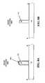
- FIGS. 2A and 2Billustrate an exemplary mesa formed consistent with the invention
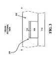
- FIG. 3illustrates an exemplary layer of Si 3 N 4 formed over the mesa of FIGS. 2A and 2B consistent with the invention
- FIGS. 4A and 4Billustrate an exemplary dummy gate formed from the Si 3 N 4 layer of FIG. 3 consistent with the invention
- FIG. 5illustrates the formation of a dielectric layer over the dummy gate and mesa of FIGS. 4A and 4B consistent with the invention
- FIG. 6illustrates the removal of the dummy gate material of FIG. 5 consistent with the invention
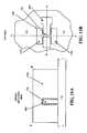
- FIGS. 7A and 7Billustrate the use of an active mask to etch a fin within the mesa of FIG. 6 consistent with the invention
- FIGS. 8A and 8Billustrate the formation, and removal, of a sacrificial oxide layer from the fin of FIGS. 7A and 7B consistent with the invention
- FIGS. 9A and 9Billustrate the formation of an exemplary gate dielectric layer in the trench of FIG. 6 consistent with the invention
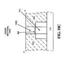
- FIGS. 10A , 10 B and 10 Cillustrate the formation of an exemplary gate within the trench of FIGS. 9A and 9B consistent with the invention
- FIGS. 11A , 11 B and 11 Cillustrate the removal of portions of the dielectric layer of FIGS. 10A , 10 B and 10 C consistent with the invention
- FIG. 12illustrates seed, oxide and buried oxide layers used to form a strained fin using epitaxial regrowth consistent with another embodiment of the invention
- FIG. 13illustrates the formation of a trench within the oxide layer of FIG. 12 consistent with another embodiment of the invention
- FIG. 14illustrates the formation of a strained semiconducting layer within the trench of FIG. 13 consistent with another embodiment of the invention
- FIG. 15illustrates the polishing of excess growth of the strained semiconducting layer of FIG. 14 consistent with another embodiment of the invention
- FIG. 16illustrates the formation of a fin spacer consistent with another embodiment of the invention.
- FIG. 17illustrates etching of the seed layer of FIG. 16 consistent with another embodiment of the invention.
- FIG. 18illustrates seed, oxide and buried oxide layers used for nano-wire formation via selective epitaxy of dissimilar semiconductors consistent with a further embodiment of the invention
- FIG. 19illustrates the formation of a trench within the oxide layer of FIG. 18 consistent with a further embodiment of the invention
- FIG. 20illustrates the formation of alternating layers of different semiconducting materials in the trench of FIG. 19 consistent with a further embodiment of the invention
- FIGS. 21A and 21Billustrate the polishing of excess material from the topmost layer of the alternating layers of FIG. 20 consistent with a further embodiment of the invention
- FIGS. 22A and 22Billustrate the removal of the oxide layer of FIGS. 21A and 21B consistent with a further embodiment of the invention.
- FIGS. 23A , 23 B and 23 Cillustrate the formation of nano-wires by removal of one of the alternating layers of dissimilar semiconducting materials of FIGS. 22A and 22B consistent with a further embodiment of the invention.
- an exemplary process for forming a tri-gate FinFETforms a silicon mesa on a FDSOI wafer.
- a dummy gatethat may include, for example, Si 3 N 4 , may be formed over the mesa and a layer of tetraethylorthosilicate (TEOS), or any other dielectric material, may then be formed over the mesa and the dummy gate.
- TEOStetraethylorthosilicate
- the dummy gatemay then be removed, leaving a trench in the shape of the eventual gate and an active mask may be used to etch a fin channel in exposed portions of the mesa within the trench.
- a gatemay then be formed in the trench over the fin to produce a tri-gate FinFET.
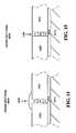
- FIG. 1illustrates a cross-section of a FDSOI wafer 100 formed in accordance with an exemplary embodiment of the present invention.
- FDSOI wafer 100may include a layer of semiconducting material 105 formed on a layer of oxide 110 .
- the layer of semiconducting material 105may include, for example, silicon, germanium or silicon-germanium, and may range, for example, from about 10 nm to about 50 nm in thickness.
- Layer 105may be used to form a fin for a FinFET device as described in more detail below.
- Oxide layer 110may be formed on a substrate comprising silicon, germanium or silicon-germanium (not shown).
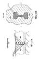
- a mesa 205may be formed from layers 105 and 115 .
- Mesa 205may be formed, for example, using a rectangular active mask and conventional etching processes.
- a conventional photoresist materialmay be patterned and etched to define a rectangular mask having dimensions ranging from about 200 nm to 1000 m in length and about 80 nm to about 250 nm in width. The areas not covered by the mask may then be etched, with the etching terminating on oxide layer 110 . The photoresist material may then be removed.
- a layer 305 of material, such as, for example, Si 3 N 4may then be formed over mesa 205 , as shown in FIG. 3 .
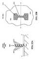
- Mask 705may be formed using a conventional photoresist material and its length may extend about 100 nm beyond mesa 205 on each end and its width may range from about 15 nm to about 30 nm after photoresist trimming.
- Mask 705may be used to remove portions of mesa 205 exposed in gate trench 605 to create fin 710 .
- the portions of mesa 205 not covered by mask 705may be etched to form fin 710 that may comprise a channel region for the final tri-gate FinFET.
- Fin 710may have a width, w, ranging, for example, from about 15 nm to about 30 nm.
- Mask 705may then be removed.
- a layer 805 of sacrificial oxidemay be formed over fin 710 .
- Sacrificial oxide layer 805may be formed on fin 710 using any conventional process.
- sacrificial oxide layer 805may be thermally grown on fin 710 .
- sacrificial oxide layer 805may be removed using a conventional process, such as, for example, a conventional etching process, to remove defects from sidewalls of fin 710 .
- a gate dielectric 905may then be formed on surfaces of fin 710 and exposed sidewalls of mesa 205 within gate trench 605 , as shown in FIGS. 9A and 9B .
- Gate dielectric 905may be thermally grown or deposited using conventional processes.
- Gate dielectric 905may include SiO, SiO 2 , SiN, SiON, HF 02 , ZrO 2 , Al 2 O 3 , HfSiO(x), HfSiO(x)N(1-x) an oxide/nitride stack, or other high-K dielectric materials.
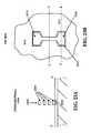
- a gate 1005may then be formed in gate trench 605 , as shown in FIGS. 10A , 10 B and 10 C.
- Gate 1005may include, for example, polysilicon or a metal, that may be deposited in gate trench 605 and then polished back to the upper surface of TEOS layer 505 using, for example, a conventional CMP process.
- TEOS layer 505 and exposed portions of gate dielectric 905may then be removed, stopping on mesa 205 , to expose oxide layer 110 , as shown in FIGS. 11A , 11 B and 11 C.
- TEOS layer 505 and exposed portions of gate dielectric 905may be removed, for example, using conventional etching processes.
- Source 1105 and drain 1110 regionsmay then be formed from exposed portions of mesa 205 to complete the tri-gate FinFET formation process.
- the resulting gate 1005is disposed on three sides of fin 710 (i.e., over the top surface of fin 710 and adjacent both side surfaces of fin 710 ), thus, producing a tri-gate FinFET.
- the tri-gate FinFETconsistent with the invention, will have better short-channel control than double-gate and single-gate devices and will have higher drive current than a double-gate FinFET for the same area.
- FIGS. 12-17illustrate an exemplary process for forming a strained FinFET fin using an epitaxial regrowth process consistent with another embodiment of the invention.
- the exemplary processmay begin with the formation of a seed layer 1210 and an oxide layer 1205 on a buried oxide (BOX) layer 1215 .
- Seed layer 1210may include, for example, germanium (Ge), though other semiconducting materials may be used, and may be formed using, for example, conventional deposition processes. Seed layer 1210 may range, for example, from about 200 ⁇ to about 1000 ⁇ in thickness.
- Oxide layer 1205may include, for example, SiO or SiO 2 , though other oxide materials may be used, and may be formed, for example, from a conventional CVD process. Oxide layer 1205 may range, for example, from about 800 ⁇ to about 1200 ⁇ in thickness.
- a trench 1305may be formed in oxide layer 1205 using, for example, conventional photolithographic and etching processes. Trench 1305 may range, for example, from about 500 ⁇ to about 5000 ⁇ in width. As further shown in FIG. 14 , a strained semiconducting layer 1405 may then be grown in trench 1305 using, for example, selective epitaxy. Growth of layer 1405 may start from Si x Ge 1-x (at “A”) and progress to silicon (at “C”). After growth of layer 1405 , excess growth may be polished off using, for example, a conventional CMP process, to form fin 1505 , as shown in FIG. 15 .
- oxide layer 1205may be removed using, for example, a conventional etching process to form a strained fin 1505 .
- a spacer 1605may then be formed over strained fin 1505 .
- Spacer 1605may include a dielectric material, such as, for example, SiO, SiO 2 , SiN, SiON, HFO 2 , ZrO 2 , Al 2 O 3 , HfSiO(x), or HfSiO(x)N(1-x) and may range, for example, from about 10 ⁇ to about 40 ⁇ in thickness.
- Seed layer 1210may then be etched away, as shown in FIG. 17 . Tensile strain in fin 1505 , that is due to confinement from seed layer 1210 , improves carrier mobility of the FinFET.
- FIGS. 18-23illustrate an exemplary process for forming multiple channel “nano-wires” in a fin of a FinFET consistent with a further embodiment of the invention.
- the formation of multiple channel nano-wires, having extremely small vertical and horizontal dimensions,can be very difficult.
- the exemplary process described with respect to FIGS. 18-23enables the formation of such structures.
- the exemplary processmay begin with the formation of a seed layer 1810 and an oxide layer 1805 on a buried oxide (BOX) layer 1815 .
- Seed layer 1810may include, for example, silicon, though other semiconducting materials may be used, and may be formed using, for example, conventional deposition processes. Seed layer 1810 may range, for example, from about 200 ⁇ to about 500 ⁇ in thickness.
- Oxide layer 1805may include, for example, SiO or SiO 2 , though other oxide materials may be used, and may be formed, for example, from a conventional CVD process. Oxide layer 1805 may range, for example, from about 800 ⁇ to about 1200 ⁇ in thickness.
- a trench 1905may be formed in oxide layer 1805 using, for example, conventional photolithographic and etching processes. Trench 1905 may range, for example, from about 500 ⁇ to about 2500 ⁇ in width. Alternating layers of different semiconducting materials may then be grown in trench 1905 using, for example, selective epitaxy, as shown in FIG. 20 . Two different semiconducting materials 2005 and 2010 may be grown, for example, in trench 1905 . Semiconducting material 2005 may include silicon, for example, and semiconducting material 2010 may include germanium, for example. One skilled in the art will recognize that other semiconducting materials may be used for the different semiconducting materials 2005 and 2010 . As further shown in FIGS. 21A and 21B , the excess material of the topmost layer of semiconducting material 2010 may be polished off using, for example, a conventional CMP process, thereby forming a planar top surface.
- Oxide layer 1805may be removed using, for example, a conventional etching process to form a fin 2205 , as shown in FIGS. 22A and 22B .
- material 2005may be removed using, for example, a conventional wet etching process, to create nano-wires 2305 .
- Etching of material 2005 in fin 2205may also result in undercutting 2310 of the FinFET source 2315 and drain 2320 regions, as shown in FIGS. 23B and 23C .
- Each of nano-wires 2305represents an extremely small channel that can independently contact the eventually formed FinFET gate (not shown).
Landscapes
- Insulated Gate Type Field-Effect Transistor (AREA)
- Thin Film Transistor (AREA)
Abstract
Description
Claims (19)
Priority Applications (1)
| Application Number | Priority Date | Filing Date | Title |
|---|---|---|---|
| US10/633,503US6855583B1 (en) | 2003-08-05 | 2003-08-05 | Method for forming tri-gate FinFET with mesa isolation |
Applications Claiming Priority (1)
| Application Number | Priority Date | Filing Date | Title |
|---|---|---|---|
| US10/633,503US6855583B1 (en) | 2003-08-05 | 2003-08-05 | Method for forming tri-gate FinFET with mesa isolation |
Publications (1)
| Publication Number | Publication Date |
|---|---|
| US6855583B1true US6855583B1 (en) | 2005-02-15 |
Family
ID=34115849
Family Applications (1)
| Application Number | Title | Priority Date | Filing Date |
|---|---|---|---|
| US10/633,503Expired - Fee RelatedUS6855583B1 (en) | 2003-08-05 | 2003-08-05 | Method for forming tri-gate FinFET with mesa isolation |
Country Status (1)
| Country | Link |
|---|---|
| US (1) | US6855583B1 (en) |
Cited By (41)
| Publication number | Priority date | Publication date | Assignee | Title |
|---|---|---|---|---|
| US20050093074A1 (en)* | 2003-11-05 | 2005-05-05 | International Business Machines Corporation | Method of fabricating a finfet |
| US20050142780A1 (en)* | 2003-12-30 | 2005-06-30 | Lee Byeong R. | Method of fabricating a fin transistor |
| US20050153486A1 (en)* | 2004-01-12 | 2005-07-14 | Advanced Micro Devices, Inc. | Method of fabricating a strained silicon channel FinFET |
| US6936516B1 (en)* | 2004-01-12 | 2005-08-30 | Advanced Micro Devices, Inc. | Replacement gate strained silicon finFET process |
| US20060231929A1 (en)* | 2003-06-26 | 2006-10-19 | Anderson Brent A | Semiconductor device having freestanding semiconductor layer |
| WO2007000690A1 (en)* | 2005-06-27 | 2007-01-04 | Nxp B.V. | Method of manufacturing a semiconductor device and semiconductor device obtained with such a method |
| US7183152B1 (en)* | 2003-08-05 | 2007-02-27 | Advanced Micro Devices, Inc. | Epitaxially grown fin for FinFET |
| US20070045748A1 (en)* | 2005-08-25 | 2007-03-01 | International Business Machines Corporation | Semiconductor structures integrating damascene-body FinFET's and planar devices on a common substrate and methods for forming such semiconductor structures |
| US20070108537A1 (en)* | 2005-11-15 | 2007-05-17 | International Business Machines Corporation | Corner dominated trigate field effect transistor |
| US20080001169A1 (en)* | 2006-03-24 | 2008-01-03 | Amberwave Systems Corporation | Lattice-mismatched semiconductor structures and related methods for device fabrication |
| US20080050898A1 (en)* | 2006-08-23 | 2008-02-28 | Hongfa Luan | Semiconductor devices and methods of manufacture thereof |
| US20080073667A1 (en)* | 2006-09-27 | 2008-03-27 | Amberwave Systems Corporation | Tri-gate field-effect transistors formed by aspect ratio trapping |
| US20080093622A1 (en)* | 2006-10-19 | 2008-04-24 | Amberwave Systems Corporation | Light-Emitter-Based Devices with Lattice-Mismatched Semiconductor Structures |
| US20080257409A1 (en)* | 2007-04-09 | 2008-10-23 | Amberwave Systems Corporation | Photovoltaics on silicon |
| CN100442445C (en)* | 2006-05-18 | 2008-12-10 | 联华电子股份有限公司 | Method for manufacturing grid and etching conductive layer |
| US20090039361A1 (en)* | 2005-05-17 | 2009-02-12 | Amberwave Systems Corporation | Lattice-mismatched semiconductor structures with reduced dislocation defect densities and related methods for device fabrication |
| US20090065047A1 (en)* | 2007-09-07 | 2009-03-12 | Amberwave Systems Corporation | Multi-Junction Solar Cells |
| WO2009044236A1 (en)* | 2007-10-03 | 2009-04-09 | Freescale Semiconductor, Inc. | Method of forming an inverted t shaped channel structure for an inverted t channel field effect transistor device |
| WO2009070252A1 (en)* | 2007-11-30 | 2009-06-04 | Advanced Micro Devices, Inc. | A hetero-structured, inverted-t field effect transistor |
| WO2009098548A1 (en)* | 2008-02-08 | 2009-08-13 | Freescale Semiconductor, Inc. | Intermediate product for a multichannel fet and process for obtaining an intermediate product |
| US20100072515A1 (en)* | 2008-09-19 | 2010-03-25 | Amberwave Systems Corporation | Fabrication and structures of crystalline material |
| US20100078680A1 (en)* | 2008-09-24 | 2010-04-01 | Amberwave Systems Corporation | Semiconductor sensor structures with reduced dislocation defect densities and related methods for the same |
| US20100176371A1 (en)* | 2009-01-09 | 2010-07-15 | Taiwan Semiconductor Manufacturing Company, Ltd. | Semiconductor Diodes Fabricated by Aspect Ratio Trapping with Coalesced Films |
| US20100176375A1 (en)* | 2009-01-09 | 2010-07-15 | Taiwan Semiconductor Manufacturing Company, Ltd. | Diode-Based Devices and Methods for Making the Same |
| US20100252861A1 (en)* | 2009-04-02 | 2010-10-07 | Taiwan Semiconductor Manufacturing Company, Ltd. | Devices Formed from a Non-Polar Plane of a Crystalline Material and Method of Making the Same |
| US20110011438A1 (en)* | 2007-04-09 | 2011-01-20 | Taiwan Semiconductor Manufacturing Company, Ltd. | Nitride-Based Multi-Junction Solar Cell Modules and Methods for Making the Same |
| US20110049568A1 (en)* | 2005-05-17 | 2011-03-03 | Taiwan Semiconductor Manufacturing Company, Ltd. | Lattice-Mismatched Semiconductor Structures with Reduced Dislocation Defect Densities and Related Methods for Device Fabrication |
| US20110086498A1 (en)* | 2006-09-27 | 2011-04-14 | Taiwan Semiconductor Manufacturing Company, Ltd. | Quantum Tunneling Devices and Circuits with Lattice-Mismatched Semiconductor Structures |
| US8183627B2 (en) | 2004-12-01 | 2012-05-22 | Taiwan Semiconductor Manufacturing Company, Ltd. | Hybrid fin field-effect transistor structures and related methods |
| US8274097B2 (en) | 2008-07-01 | 2012-09-25 | Taiwan Semiconductor Manufacturing Company, Ltd. | Reduction of edge effects from aspect ratio trapping |
| US8329541B2 (en) | 2007-06-15 | 2012-12-11 | Taiwan Semiconductor Manufacturing Company, Ltd. | InP-based transistor fabrication |
| US8384196B2 (en) | 2008-09-19 | 2013-02-26 | Taiwan Semiconductor Manufacturing Company, Ltd. | Formation of devices by epitaxial layer overgrowth |
| US8822248B2 (en) | 2008-06-03 | 2014-09-02 | Taiwan Semiconductor Manufacturing Company, Ltd. | Epitaxial growth of crystalline material |
| US8847279B2 (en) | 2006-09-07 | 2014-09-30 | Taiwan Semiconductor Manufacturing Company, Ltd. | Defect reduction using aspect ratio trapping |
| US8981427B2 (en) | 2008-07-15 | 2015-03-17 | Taiwan Semiconductor Manufacturing Company, Ltd. | Polishing of small composite semiconductor materials |
| US9252014B2 (en) | 2013-09-04 | 2016-02-02 | Globalfoundries Inc. | Trench sidewall protection for selective epitaxial semiconductor material formation |
| US9343529B2 (en)* | 2014-09-05 | 2016-05-17 | International Business Machines Corporation | Method of formation of germanium nanowires on bulk substrates |
| US11786334B2 (en) | 2016-12-14 | 2023-10-17 | Virtual Incision Corporation | Releasable attachment device for coupling to medical devices and related systems and methods |
| US11806097B2 (en) | 2013-03-14 | 2023-11-07 | Board Of Regents Of The University Of Nebraska | Methods, systems, and devices relating to robotic surgical devices, end effectors, and controllers |
| US12109079B2 (en) | 2016-11-22 | 2024-10-08 | Board Of Regents Of The University Of Nebraska | Gross positioning device and related systems and methods |
| US12150722B2 (en) | 2020-07-06 | 2024-11-26 | Virtual Incision Corporation | Surgical robot positioning system and related devices and methods |
Citations (5)
| Publication number | Priority date | Publication date | Assignee | Title |
|---|---|---|---|---|
| US6525403B2 (en)* | 2000-09-28 | 2003-02-25 | Kabushiki Kaisha Toshiba | Semiconductor device having MIS field effect transistors or three-dimensional structure |
| US6610576B2 (en)* | 2001-12-13 | 2003-08-26 | International Business Machines Corporation | Method for forming asymmetric dual gate transistor |
| US6657252B2 (en)* | 2002-03-19 | 2003-12-02 | International Business Machines Corporation | FinFET CMOS with NVRAM capability |
| US20040036126A1 (en)* | 2002-08-23 | 2004-02-26 | Chau Robert S. | Tri-gate devices and methods of fabrication |
| US6727546B2 (en)* | 2000-11-13 | 2004-04-27 | Advanced Micro Devices, Inc. | Self-aligned triple gate silicon-on-insulator (SOI) device |
- 2003
- 2003-08-05USUS10/633,503patent/US6855583B1/ennot_activeExpired - Fee Related
Patent Citations (5)
| Publication number | Priority date | Publication date | Assignee | Title |
|---|---|---|---|---|
| US6525403B2 (en)* | 2000-09-28 | 2003-02-25 | Kabushiki Kaisha Toshiba | Semiconductor device having MIS field effect transistors or three-dimensional structure |
| US6727546B2 (en)* | 2000-11-13 | 2004-04-27 | Advanced Micro Devices, Inc. | Self-aligned triple gate silicon-on-insulator (SOI) device |
| US6610576B2 (en)* | 2001-12-13 | 2003-08-26 | International Business Machines Corporation | Method for forming asymmetric dual gate transistor |
| US6657252B2 (en)* | 2002-03-19 | 2003-12-02 | International Business Machines Corporation | FinFET CMOS with NVRAM capability |
| US20040036126A1 (en)* | 2002-08-23 | 2004-02-26 | Chau Robert S. | Tri-gate devices and methods of fabrication |
Non-Patent Citations (5)
| Title |
|---|
| Digh Hisamoto et al., "FinFET-A Self-Aligned Double-Gate MOSFET Scalable to 20 nm," IEEE Transactions on Electron Devices, vol. 47, No. 12, Dec. 2000, pp. 2320-2325. |
| Xuejue Huang et al., "Sub 50-nm FinFET: PMOS," 1999 IEEE, IEDM, pp. 67-70. |
| Xuejue Huang et al., "Sub-50 nm P-Channel FinFET," IEEE Transactions on Electron Devices, vol. 48, No. 5, May 2001, pp. 880-886. |
| Yang-Kyu Choi et al., "Nanoscale CMOS Spacer FinFET for the Terabit Era," IEEE Electron Device Letters, vol. 23, No. 1, Jan. 2002, pp. 25-27. |
| Yang-Kyu Choi et al., "Sub-20nm CMOS FinFET Technologies," 2001 IEEE, IEDM, pp. 421-424. |
Cited By (126)
| Publication number | Priority date | Publication date | Assignee | Title |
|---|---|---|---|---|
| US7709892B2 (en)* | 2003-06-26 | 2010-05-04 | International Business Machines Corporation | Semiconductor device having freestanding semiconductor layer |
| US20060231929A1 (en)* | 2003-06-26 | 2006-10-19 | Anderson Brent A | Semiconductor device having freestanding semiconductor layer |
| US7183152B1 (en)* | 2003-08-05 | 2007-02-27 | Advanced Micro Devices, Inc. | Epitaxially grown fin for FinFET |
| US7247908B2 (en) | 2003-11-05 | 2007-07-24 | International Business Machines Corporation | Method of fabricating a FinFET |
| US20050093074A1 (en)* | 2003-11-05 | 2005-05-05 | International Business Machines Corporation | Method of fabricating a finfet |
| US6962843B2 (en)* | 2003-11-05 | 2005-11-08 | International Business Machines Corporation | Method of fabricating a finfet |
| US20050280090A1 (en)* | 2003-11-05 | 2005-12-22 | Anderson Brent A | Method of fabricating a FinFET |
| US7179713B2 (en)* | 2003-12-30 | 2007-02-20 | Dongbu Electronics Co., Ltd. | Method of fabricating a fin transistor |
| US20050142780A1 (en)* | 2003-12-30 | 2005-06-30 | Lee Byeong R. | Method of fabricating a fin transistor |
| KR101065049B1 (en)* | 2004-01-12 | 2011-09-19 | 글로벌파운드리즈 인크. | Modified Pinpet Channel Manufacturing Method |
| US7138302B2 (en)* | 2004-01-12 | 2006-11-21 | Advanced Micro Devices, Inc. | Method of fabricating an integrated circuit channel region |
| US6936516B1 (en)* | 2004-01-12 | 2005-08-30 | Advanced Micro Devices, Inc. | Replacement gate strained silicon finFET process |
| US20050153486A1 (en)* | 2004-01-12 | 2005-07-14 | Advanced Micro Devices, Inc. | Method of fabricating a strained silicon channel FinFET |
| US8183627B2 (en) | 2004-12-01 | 2012-05-22 | Taiwan Semiconductor Manufacturing Company, Ltd. | Hybrid fin field-effect transistor structures and related methods |
| US9153645B2 (en) | 2005-05-17 | 2015-10-06 | Taiwan Semiconductor Manufacturing Company, Ltd. | Lattice-mismatched semiconductor structures with reduced dislocation defect densities and related methods for device fabrication |
| US20090039361A1 (en)* | 2005-05-17 | 2009-02-12 | Amberwave Systems Corporation | Lattice-mismatched semiconductor structures with reduced dislocation defect densities and related methods for device fabrication |
| US9431243B2 (en) | 2005-05-17 | 2016-08-30 | Taiwan Semiconductor Manufacturing Company, Ltd. | Lattice-mismatched semiconductor structures with reduced dislocation defect densities and related methods for device fabrication |
| US20110049568A1 (en)* | 2005-05-17 | 2011-03-03 | Taiwan Semiconductor Manufacturing Company, Ltd. | Lattice-Mismatched Semiconductor Structures with Reduced Dislocation Defect Densities and Related Methods for Device Fabrication |
| US10522629B2 (en) | 2005-05-17 | 2019-12-31 | Taiwan Semiconductor Manufacturing Company, Ltd. | Lattice-mismatched semiconductor structures with reduced dislocation defect densities and related methods for device fabrication |
| US8987028B2 (en) | 2005-05-17 | 2015-03-24 | Taiwan Semiconductor Manufacturing Company, Ltd. | Lattice-mismatched semiconductor structures with reduced dislocation defect densities and related methods for device fabrication |
| US8629477B2 (en) | 2005-05-17 | 2014-01-14 | Taiwan Semiconductor Manufacturing Company, Ltd. | Lattice-mismatched semiconductor structures with reduced dislocation defect densities and related methods for device fabrication |
| US11251272B2 (en) | 2005-05-17 | 2022-02-15 | Taiwan Semiconductor Manufacturing Company, Ltd. | Lattice-mismatched semiconductor structures with reduced dislocation defect densities and related methods for device fabrication |
| US9219112B2 (en) | 2005-05-17 | 2015-12-22 | Taiwan Semiconductor Manufacturing Company, Ltd. | Lattice-mismatched semiconductor structures with reduced dislocation defect densities and related methods for device fabrication |
| US8324660B2 (en) | 2005-05-17 | 2012-12-04 | Taiwan Semiconductor Manufacturing Company, Ltd. | Lattice-mismatched semiconductor structures with reduced dislocation defect densities and related methods for device fabrication |
| US8519436B2 (en) | 2005-05-17 | 2013-08-27 | Taiwan Semiconductor Manufacturing Company, Ltd. | Lattice-mismatched semiconductor structures with reduced dislocation defect densities and related methods for device fabrication |
| US8796734B2 (en) | 2005-05-17 | 2014-08-05 | Taiwan Semiconductor Manufacturing Company, Ltd. | Lattice-mismatched semiconductor structures with reduced dislocation defect densities and related methods for device fabrication |
| WO2007000690A1 (en)* | 2005-06-27 | 2007-01-04 | Nxp B.V. | Method of manufacturing a semiconductor device and semiconductor device obtained with such a method |
| US20070045748A1 (en)* | 2005-08-25 | 2007-03-01 | International Business Machines Corporation | Semiconductor structures integrating damascene-body FinFET's and planar devices on a common substrate and methods for forming such semiconductor structures |
| US7879660B2 (en) | 2005-08-25 | 2011-02-01 | International Business Machines Corporation | Semiconductor structures integrating damascene-body FinFET's and planar devices on a common substrate and methods for forming such semiconductor structures |
| US7352034B2 (en)* | 2005-08-25 | 2008-04-01 | International Business Machines Corporation | Semiconductor structures integrating damascene-body FinFET's and planar devices on a common substrate and methods for forming such semiconductor structures |
| US20080048265A1 (en)* | 2005-08-25 | 2008-02-28 | International Business Machines Corporation | Semiconductor structures integrating damascene-body finfet's and planar devices on a common substrate and methods for forming such semiconductor structures |
| US20080050866A1 (en)* | 2005-08-25 | 2008-02-28 | International Business Machines Corporation | Semiconductor structures integrating damascene-body finfet's and planar devices on a common substrate and methods for forming such semiconductor structures |
| US7692250B2 (en) | 2005-08-25 | 2010-04-06 | International Business Machines Corporation | Semiconductor structures integrating damascene-body FinFET's and planar devices on a common substrate and methods for forming such semiconductor structures |
| US7473605B2 (en) | 2005-11-15 | 2009-01-06 | International Business Machines Corporation | Corner dominated trigate field effect transistor |
| US20080090361A1 (en)* | 2005-11-15 | 2008-04-17 | Anderson Brent A | Corner dominated trigate field effect transistor |
| CN100487917C (en)* | 2005-11-15 | 2009-05-13 | 国际商业机器公司 | Field effect transistor and its forming method |
| US20070108537A1 (en)* | 2005-11-15 | 2007-05-17 | International Business Machines Corporation | Corner dominated trigate field effect transistor |
| US7326976B2 (en) | 2005-11-15 | 2008-02-05 | International Business Machines Corporation | Corner dominated trigate field effect transistor |
| US7777250B2 (en) | 2006-03-24 | 2010-08-17 | Taiwan Semiconductor Manufacturing Company, Ltd. | Lattice-mismatched semiconductor structures and related methods for device fabrication |
| US10074536B2 (en) | 2006-03-24 | 2018-09-11 | Taiwan Semiconductor Manufacturing Company, Ltd. | Lattice-mismatched semiconductor structures and related methods for device fabrication |
| US20100213511A1 (en)* | 2006-03-24 | 2010-08-26 | Taiwan Semiconductor Manufacturing Company, Ltd. | Lattice-Mismatched Semiconductor Structures and Related Methods for Device Fabrication |
| US20080001169A1 (en)* | 2006-03-24 | 2008-01-03 | Amberwave Systems Corporation | Lattice-mismatched semiconductor structures and related methods for device fabrication |
| US8878243B2 (en) | 2006-03-24 | 2014-11-04 | Taiwan Semiconductor Manufacturing Company, Ltd. | Lattice-mismatched semiconductor structures and related methods for device fabrication |
| CN100442445C (en)* | 2006-05-18 | 2008-12-10 | 联华电子股份有限公司 | Method for manufacturing grid and etching conductive layer |
| US20080050898A1 (en)* | 2006-08-23 | 2008-02-28 | Hongfa Luan | Semiconductor devices and methods of manufacture thereof |
| US9318325B2 (en) | 2006-09-07 | 2016-04-19 | Taiwan Semiconductor Manufacturing Company, Ltd. | Defect reduction using aspect ratio trapping |
| US9818819B2 (en) | 2006-09-07 | 2017-11-14 | Taiwan Semiconductor Manufacturing Company, Ltd. | Defect reduction using aspect ratio trapping |
| US8847279B2 (en) | 2006-09-07 | 2014-09-30 | Taiwan Semiconductor Manufacturing Company, Ltd. | Defect reduction using aspect ratio trapping |
| US20080073667A1 (en)* | 2006-09-27 | 2008-03-27 | Amberwave Systems Corporation | Tri-gate field-effect transistors formed by aspect ratio trapping |
| US7799592B2 (en) | 2006-09-27 | 2010-09-21 | Taiwan Semiconductor Manufacturing Company, Ltd. | Tri-gate field-effect transistors formed by aspect ratio trapping |
| WO2008039495A1 (en)* | 2006-09-27 | 2008-04-03 | Amberwave Systems Corporation | Tri-gate field-effect transistors formed by aspect ratio trapping |
| US8860160B2 (en) | 2006-09-27 | 2014-10-14 | Taiwan Semiconductor Manufacturing Company, Ltd. | Quantum tunneling devices and circuits with lattice-mismatched semiconductor structures |
| US8216951B2 (en) | 2006-09-27 | 2012-07-10 | Taiwan Semiconductor Manufacturing Company, Ltd. | Quantum tunneling devices and circuits with lattice-mismatched semiconductor structures |
| US9105522B2 (en) | 2006-09-27 | 2015-08-11 | Taiwan Semiconductor Manufacturing Company, Ltd. | Quantum tunneling devices and circuits with lattice-mismatched semiconductor structures |
| US9559712B2 (en) | 2006-09-27 | 2017-01-31 | Taiwan Semiconductor Manufacturing Company, Ltd. | Quantum tunneling devices and circuits with lattice-mismatched semiconductor structures |
| US20110086498A1 (en)* | 2006-09-27 | 2011-04-14 | Taiwan Semiconductor Manufacturing Company, Ltd. | Quantum Tunneling Devices and Circuits with Lattice-Mismatched Semiconductor Structures |
| US8629047B2 (en) | 2006-09-27 | 2014-01-14 | Taiwan Semiconductor Manufacturing Company, Ltd. | Quantum tunneling devices and circuits with lattice-mismatched semiconductor structures |
| US20080093622A1 (en)* | 2006-10-19 | 2008-04-24 | Amberwave Systems Corporation | Light-Emitter-Based Devices with Lattice-Mismatched Semiconductor Structures |
| US10468551B2 (en) | 2006-10-19 | 2019-11-05 | Taiwan Semiconductor Manufacturing Company, Ltd. | Light-emitter-based devices with lattice-mismatched semiconductor structures |
| US8502263B2 (en) | 2006-10-19 | 2013-08-06 | Taiwan Semiconductor Manufacturing Company, Ltd. | Light-emitter-based devices with lattice-mismatched semiconductor structures |
| US9543472B2 (en) | 2007-04-09 | 2017-01-10 | Taiwan Semiconductor Manufacturing Company, Ltd. | Diode-based devices and methods for making the same |
| US20080257409A1 (en)* | 2007-04-09 | 2008-10-23 | Amberwave Systems Corporation | Photovoltaics on silicon |
| US9853118B2 (en) | 2007-04-09 | 2017-12-26 | Taiwan Semiconductor Manufacturing Company, Ltd. | Diode-based devices and methods for making the same |
| US9449868B2 (en) | 2007-04-09 | 2016-09-20 | Taiwan Semiconductor Manufacutring Company, Ltd. | Methods of forming semiconductor diodes by aspect ratio trapping with coalesced films |
| US20110011438A1 (en)* | 2007-04-09 | 2011-01-20 | Taiwan Semiconductor Manufacturing Company, Ltd. | Nitride-Based Multi-Junction Solar Cell Modules and Methods for Making the Same |
| US9853176B2 (en) | 2007-04-09 | 2017-12-26 | Taiwan Semiconductor Manufacturing Company, Ltd. | Nitride-based multi-junction solar cell modules and methods for making the same |
| US8624103B2 (en) | 2007-04-09 | 2014-01-07 | Taiwan Semiconductor Manufacturing Company, Ltd. | Nitride-based multi-junction solar cell modules and methods for making the same |
| US9040331B2 (en) | 2007-04-09 | 2015-05-26 | Taiwan Semiconductor Manufacturing Company, Ltd. | Diode-based devices and methods for making the same |
| US10680126B2 (en) | 2007-04-09 | 2020-06-09 | Taiwan Semiconductor Manufacturing Company, Ltd. | Photovoltaics on silicon |
| US9231073B2 (en) | 2007-04-09 | 2016-01-05 | Taiwan Semiconductor Manufacturing Company, Ltd. | Diode-based devices and methods for making the same |
| US9508890B2 (en) | 2007-04-09 | 2016-11-29 | Taiwan Semiconductor Manufacturing Company, Ltd. | Photovoltaics on silicon |
| US8329541B2 (en) | 2007-06-15 | 2012-12-11 | Taiwan Semiconductor Manufacturing Company, Ltd. | InP-based transistor fabrication |
| US9780190B2 (en) | 2007-06-15 | 2017-10-03 | Taiwan Semiconductor Manufacturing Company, Ltd. | InP-based transistor fabrication |
| US10002981B2 (en) | 2007-09-07 | 2018-06-19 | Taiwan Semiconductor Manufacturing Company, Ltd. | Multi-junction solar cells |
| US20090065047A1 (en)* | 2007-09-07 | 2009-03-12 | Amberwave Systems Corporation | Multi-Junction Solar Cells |
| US8344242B2 (en) | 2007-09-07 | 2013-01-01 | Taiwan Semiconductor Manufacturing Company, Ltd. | Multi-junction solar cells |
| WO2009044236A1 (en)* | 2007-10-03 | 2009-04-09 | Freescale Semiconductor, Inc. | Method of forming an inverted t shaped channel structure for an inverted t channel field effect transistor device |
| US20100311213A1 (en)* | 2007-10-03 | 2010-12-09 | Freescale Semiconductor, Inc. | Method of forming an inverted t shaped channel structure for an inverted t channel field effect transistor device |
| US8552501B2 (en) | 2007-10-03 | 2013-10-08 | Freescale Semiconductor, Inc. | Method of forming an inverted T shaped channel structure for an inverted T channel field effect transistor device |
| US8158484B2 (en) | 2007-10-03 | 2012-04-17 | Freescale Semiconductor, Inc. | Method of forming an inverted T shaped channel structure for an inverted T channel field effect transistor device |
| CN101884107B (en)* | 2007-11-30 | 2013-02-13 | 先进微装置公司 | Hetero-structured, inverted-t field effect transistor |
| US20120309141A1 (en)* | 2007-11-30 | 2012-12-06 | Advanced Micro Devices, Inc. | Hetero-structured inverted-t field effect transistor |
| WO2009070252A1 (en)* | 2007-11-30 | 2009-06-04 | Advanced Micro Devices, Inc. | A hetero-structured, inverted-t field effect transistor |
| US8815658B2 (en)* | 2007-11-30 | 2014-08-26 | Advanced Micro Devices, Inc. | Hetero-structured inverted-T field effect transistor |
| WO2009098548A1 (en)* | 2008-02-08 | 2009-08-13 | Freescale Semiconductor, Inc. | Intermediate product for a multichannel fet and process for obtaining an intermediate product |
| US8293608B2 (en)* | 2008-02-08 | 2012-10-23 | Freescale Semiconductor, Inc. | Intermediate product for a multichannel FET and process for obtaining an intermediate product |
| US20110003451A1 (en)* | 2008-02-08 | 2011-01-06 | Freescale Semiconductor, Inc. | Intermediate product for a multichannel fet and process for obtaining an intermediate product |
| US8822248B2 (en) | 2008-06-03 | 2014-09-02 | Taiwan Semiconductor Manufacturing Company, Ltd. | Epitaxial growth of crystalline material |
| US10961639B2 (en) | 2008-06-03 | 2021-03-30 | Taiwan Semiconductor Manufacturing Company, Ltd. | Epitaxial growth of crystalline material |
| US9365949B2 (en) | 2008-06-03 | 2016-06-14 | Taiwan Semiconductor Manufacturing Company, Ltd. | Epitaxial growth of crystalline material |
| US8629045B2 (en) | 2008-07-01 | 2014-01-14 | Taiwan Semiconductor Manufacturing Company, Ltd. | Reduction of edge effects from aspect ratio trapping |
| US9640395B2 (en) | 2008-07-01 | 2017-05-02 | Taiwan Semiconductor Manufacturing Company, Ltd. | Reduction of edge effects from aspect ratio trapping |
| US8274097B2 (en) | 2008-07-01 | 2012-09-25 | Taiwan Semiconductor Manufacturing Company, Ltd. | Reduction of edge effects from aspect ratio trapping |
| US9356103B2 (en) | 2008-07-01 | 2016-05-31 | Taiwan Semiconductor Manufacturing Company, Ltd. | Reduction of edge effects from aspect ratio trapping |
| US8994070B2 (en) | 2008-07-01 | 2015-03-31 | Taiwan Semiconductor Manufacturing Company, Ltd. | Reduction of edge effects from aspect ratio trapping |
| US9287128B2 (en) | 2008-07-15 | 2016-03-15 | Taiwan Semiconductor Manufacturing Company, Ltd. | Polishing of small composite semiconductor materials |
| US8981427B2 (en) | 2008-07-15 | 2015-03-17 | Taiwan Semiconductor Manufacturing Company, Ltd. | Polishing of small composite semiconductor materials |
| US9607846B2 (en) | 2008-07-15 | 2017-03-28 | Taiwan Semiconductor Manufacturing Company, Ltd. | Polishing of small composite semiconductor materials |
| US9984872B2 (en) | 2008-09-19 | 2018-05-29 | Taiwan Semiconductor Manufacturing Company, Ltd. | Fabrication and structures of crystalline material |
| US8384196B2 (en) | 2008-09-19 | 2013-02-26 | Taiwan Semiconductor Manufacturing Company, Ltd. | Formation of devices by epitaxial layer overgrowth |
| US9934967B2 (en) | 2008-09-19 | 2018-04-03 | Taiwan Semiconductor Manufacturing Co., Ltd. | Formation of devices by epitaxial layer overgrowth |
| US20100072515A1 (en)* | 2008-09-19 | 2010-03-25 | Amberwave Systems Corporation | Fabrication and structures of crystalline material |
| US9455299B2 (en) | 2008-09-24 | 2016-09-27 | Taiwan Semiconductor Manufacturing Company, Ltd. | Methods for semiconductor sensor structures with reduced dislocation defect densities |
| US8809106B2 (en) | 2008-09-24 | 2014-08-19 | Taiwan Semiconductor Manufacturing Company, Ltd. | Method for semiconductor sensor structures with reduced dislocation defect densities |
| US20100078680A1 (en)* | 2008-09-24 | 2010-04-01 | Amberwave Systems Corporation | Semiconductor sensor structures with reduced dislocation defect densities and related methods for the same |
| US8253211B2 (en) | 2008-09-24 | 2012-08-28 | Taiwan Semiconductor Manufacturing Company, Ltd. | Semiconductor sensor structures with reduced dislocation defect densities |
| US9105549B2 (en) | 2008-09-24 | 2015-08-11 | Taiwan Semiconductor Manufacturing Company, Ltd. | Semiconductor sensor structures with reduced dislocation defect densities |
| US8304805B2 (en) | 2009-01-09 | 2012-11-06 | Taiwan Semiconductor Manufacturing Company, Ltd. | Semiconductor diodes fabricated by aspect ratio trapping with coalesced films |
| US20100176375A1 (en)* | 2009-01-09 | 2010-07-15 | Taiwan Semiconductor Manufacturing Company, Ltd. | Diode-Based Devices and Methods for Making the Same |
| US8237151B2 (en) | 2009-01-09 | 2012-08-07 | Taiwan Semiconductor Manufacturing Company, Ltd. | Diode-based devices and methods for making the same |
| US8765510B2 (en) | 2009-01-09 | 2014-07-01 | Taiwan Semiconductor Manufacturing Company, Ltd. | Semiconductor diodes fabricated by aspect ratio trapping with coalesced films |
| US20100176371A1 (en)* | 2009-01-09 | 2010-07-15 | Taiwan Semiconductor Manufacturing Company, Ltd. | Semiconductor Diodes Fabricated by Aspect Ratio Trapping with Coalesced Films |
| US9029908B2 (en) | 2009-01-09 | 2015-05-12 | Taiwan Semiconductor Manufacturing Company, Ltd. | Semiconductor diodes fabricated by aspect ratio trapping with coalesced films |
| US20100252861A1 (en)* | 2009-04-02 | 2010-10-07 | Taiwan Semiconductor Manufacturing Company, Ltd. | Devices Formed from a Non-Polar Plane of a Crystalline Material and Method of Making the Same |
| US9576951B2 (en) | 2009-04-02 | 2017-02-21 | Taiwan Semiconductor Manufacturing Company, Ltd. | Devices formed from a non-polar plane of a crystalline material and method of making the same |
| US9299562B2 (en) | 2009-04-02 | 2016-03-29 | Taiwan Semiconductor Manufacturing Company, Ltd. | Devices formed from a non-polar plane of a crystalline material and method of making the same |
| US8629446B2 (en) | 2009-04-02 | 2014-01-14 | Taiwan Semiconductor Manufacturing Company, Ltd. | Devices formed from a non-polar plane of a crystalline material and method of making the same |
| US11806097B2 (en) | 2013-03-14 | 2023-11-07 | Board Of Regents Of The University Of Nebraska | Methods, systems, and devices relating to robotic surgical devices, end effectors, and controllers |
| US12336777B2 (en) | 2013-03-14 | 2025-06-24 | Board Of Regents Of The University Of Nebraska | Methods, systems, and devices relating to robotic surgical devices, end effectors, and controllers |
| US9252014B2 (en) | 2013-09-04 | 2016-02-02 | Globalfoundries Inc. | Trench sidewall protection for selective epitaxial semiconductor material formation |
| US9269575B2 (en) | 2013-09-04 | 2016-02-23 | Globalfoundries Inc. | Trench sidewall protection for selective epitaxial semiconductor material formation |
| US9343529B2 (en)* | 2014-09-05 | 2016-05-17 | International Business Machines Corporation | Method of formation of germanium nanowires on bulk substrates |
| US10217818B2 (en) | 2014-09-05 | 2019-02-26 | International Business Machines Corporation | Method of formation of germanium nanowires on bulk substrates |
| US12109079B2 (en) | 2016-11-22 | 2024-10-08 | Board Of Regents Of The University Of Nebraska | Gross positioning device and related systems and methods |
| US11786334B2 (en) | 2016-12-14 | 2023-10-17 | Virtual Incision Corporation | Releasable attachment device for coupling to medical devices and related systems and methods |
| US12150722B2 (en) | 2020-07-06 | 2024-11-26 | Virtual Incision Corporation | Surgical robot positioning system and related devices and methods |
Similar Documents
| Publication | Publication Date | Title |
|---|---|---|
| US6855583B1 (en) | Method for forming tri-gate FinFET with mesa isolation | |
| US7541267B1 (en) | Reversed T-shaped finfet | |
| US6872647B1 (en) | Method for forming multiple fins in a semiconductor device | |
| US6645797B1 (en) | Method for forming fins in a FinFET device using sacrificial carbon layer | |
| US10170375B2 (en) | FinFET devices with unique fin shape and the fabrication thereof | |
| US7084018B1 (en) | Sacrificial oxide for minimizing box undercut in damascene FinFET | |
| US7186599B2 (en) | Narrow-body damascene tri-gate FinFET | |
| US6709982B1 (en) | Double spacer FinFET formation | |
| US9978870B2 (en) | FinFET with buried insulator layer and method for forming | |
| US6897527B2 (en) | Strained channel FinFET | |
| US6686231B1 (en) | Damascene gate process with sacrificial oxide in semiconductor devices | |
| US6764884B1 (en) | Method for forming a gate in a FinFET device and thinning a fin in a channel region of the FinFET device | |
| US20200035784A1 (en) | Semiconductor device and manufacturing method thereof | |
| US20060216897A1 (en) | Semiconductor device having a round-shaped nano-wire transistor channel and method of manufacturing same | |
| US6855989B1 (en) | Damascene finfet gate with selective metal interdiffusion | |
| US9412850B1 (en) | Method of trimming fin structure | |
| US11469146B2 (en) | Methods of performing fin cut etch processes for FinFET semiconductor devices | |
| US7041542B2 (en) | Damascene tri-gate FinFET | |
| US6967175B1 (en) | Damascene gate semiconductor processing with local thinning of channel region | |
| US7416925B2 (en) | Doped structure for finfet devices | |
| US9324868B2 (en) | Epitaxial growth of silicon for FinFETS with non-rectangular cross-sections | |
| CN104217948B (en) | Semiconductor manufacturing method |
Legal Events
| Date | Code | Title | Description |
|---|---|---|---|
| AS | Assignment | Owner name:ADVANCED MICRO DEVICES, INC., CALIFORNIA Free format text:ASSIGNMENT OF ASSIGNORS INTEREST;ASSIGNORS:KRIVOKAPIC, ZORAN;AN, JUDY XILIN;YU, BIN;REEL/FRAME:014369/0843;SIGNING DATES FROM 20030516 TO 20030602 | |
| FEPP | Fee payment procedure | Free format text:PAYOR NUMBER ASSIGNED (ORIGINAL EVENT CODE: ASPN); ENTITY STATUS OF PATENT OWNER: LARGE ENTITY | |
| FPAY | Fee payment | Year of fee payment:4 | |
| AS | Assignment | Owner name:GLOBALFOUNDRIES INC., CAYMAN ISLANDS Free format text:AFFIRMATION OF PATENT ASSIGNMENT;ASSIGNOR:ADVANCED MICRO DEVICES, INC.;REEL/FRAME:023119/0083 Effective date:20090630 | |
| FPAY | Fee payment | Year of fee payment:8 | |
| REMI | Maintenance fee reminder mailed | ||
| LAPS | Lapse for failure to pay maintenance fees | ||
| STCH | Information on status: patent discontinuation | Free format text:PATENT EXPIRED DUE TO NONPAYMENT OF MAINTENANCE FEES UNDER 37 CFR 1.362 | |
| FP | Lapsed due to failure to pay maintenance fee | Effective date:20170215 | |
| AS | Assignment | Owner name:GLOBALFOUNDRIES U.S. INC., NEW YORK Free format text:RELEASE BY SECURED PARTY;ASSIGNOR:WILMINGTON TRUST, NATIONAL ASSOCIATION;REEL/FRAME:056987/0001 Effective date:20201117 |