US6852926B2 - Packaging microelectromechanical structures - Google Patents
Packaging microelectromechanical structuresDownload PDFInfo
- Publication number
- US6852926B2 US6852926B2US10/106,728US10672802AUS6852926B2US 6852926 B2US6852926 B2US 6852926B2US 10672802 AUS10672802 AUS 10672802AUS 6852926 B2US6852926 B2US 6852926B2
- Authority
- US
- United States
- Prior art keywords
- semiconductor structure
- structures
- cavity
- interconnection layer
- semiconductor
- Prior art date
- Legal status (The legal status is an assumption and is not a legal conclusion. Google has not performed a legal analysis and makes no representation as to the accuracy of the status listed.)
- Expired - Lifetime
Links
- 238000004806packaging method and processMethods0.000titledescription5
- 239000004065semiconductorSubstances0.000claimsabstractdescription41
- 230000008878couplingEffects0.000claims1
- 238000010168coupling processMethods0.000claims1
- 238000005859coupling reactionMethods0.000claims1
- 239000000463materialSubstances0.000claims1
- 238000000034methodMethods0.000abstractdescription9
- 238000007789sealingMethods0.000abstractdescription7
- 235000012431wafersNutrition0.000description7
- 229910000679solderInorganic materials0.000description6
- 238000013459approachMethods0.000description3
- 239000011521glassSubstances0.000description3
- 238000004519manufacturing processMethods0.000description3
- PCHJSUWPFVWCPO-UHFFFAOYSA-NgoldChemical compound[Au]PCHJSUWPFVWCPO-UHFFFAOYSA-N0.000description2
- 229910052737goldInorganic materials0.000description2
- 239000010931goldSubstances0.000description2
- 238000012986modificationMethods0.000description2
- 230000004048modificationEffects0.000description2
- 239000000853adhesiveSubstances0.000description1
- 230000001070adhesive effectEffects0.000description1
- 239000000919ceramicSubstances0.000description1
- 230000007123defenseEffects0.000description1
- 238000005516engineering processMethods0.000description1
- 239000000945fillerSubstances0.000description1
- 238000007667floatingMethods0.000description1
- 230000000135prohibitive effectEffects0.000description1
Images


Classifications
- B—PERFORMING OPERATIONS; TRANSPORTING
- B81—MICROSTRUCTURAL TECHNOLOGY
- B81B—MICROSTRUCTURAL DEVICES OR SYSTEMS, e.g. MICROMECHANICAL DEVICES
- B81B7/00—Microstructural systems; Auxiliary parts of microstructural devices or systems
- B81B7/0006—Interconnects
- H—ELECTRICITY
- H01—ELECTRIC ELEMENTS
- H01L—SEMICONDUCTOR DEVICES NOT COVERED BY CLASS H10
- H01L23/00—Details of semiconductor or other solid state devices
- H01L23/02—Containers; Seals
- H01L23/10—Containers; Seals characterised by the material or arrangement of seals between parts, e.g. between cap and base of the container or between leads and walls of the container
- H—ELECTRICITY
- H01—ELECTRIC ELEMENTS
- H01L—SEMICONDUCTOR DEVICES NOT COVERED BY CLASS H10
- H01L2224/00—Indexing scheme for arrangements for connecting or disconnecting semiconductor or solid-state bodies and methods related thereto as covered by H01L24/00
- H01L2224/01—Means for bonding being attached to, or being formed on, the surface to be connected, e.g. chip-to-package, die-attach, "first-level" interconnects; Manufacturing methods related thereto
- H01L2224/02—Bonding areas; Manufacturing methods related thereto
- H01L2224/04—Structure, shape, material or disposition of the bonding areas prior to the connecting process
- H01L2224/05—Structure, shape, material or disposition of the bonding areas prior to the connecting process of an individual bonding area
- H01L2224/0554—External layer
- H01L2224/0556—Disposition
- H01L2224/05567—Disposition the external layer being at least partially embedded in the surface
- H—ELECTRICITY
- H01—ELECTRIC ELEMENTS
- H01L—SEMICONDUCTOR DEVICES NOT COVERED BY CLASS H10
- H01L2224/00—Indexing scheme for arrangements for connecting or disconnecting semiconductor or solid-state bodies and methods related thereto as covered by H01L24/00
- H01L2224/01—Means for bonding being attached to, or being formed on, the surface to be connected, e.g. chip-to-package, die-attach, "first-level" interconnects; Manufacturing methods related thereto
- H01L2224/02—Bonding areas; Manufacturing methods related thereto
- H01L2224/04—Structure, shape, material or disposition of the bonding areas prior to the connecting process
- H01L2224/05—Structure, shape, material or disposition of the bonding areas prior to the connecting process of an individual bonding area
- H01L2224/0554—External layer
- H01L2224/0556—Disposition
- H01L2224/05568—Disposition the whole external layer protruding from the surface
- H—ELECTRICITY
- H01—ELECTRIC ELEMENTS
- H01L—SEMICONDUCTOR DEVICES NOT COVERED BY CLASS H10
- H01L2224/00—Indexing scheme for arrangements for connecting or disconnecting semiconductor or solid-state bodies and methods related thereto as covered by H01L24/00
- H01L2224/01—Means for bonding being attached to, or being formed on, the surface to be connected, e.g. chip-to-package, die-attach, "first-level" interconnects; Manufacturing methods related thereto
- H01L2224/02—Bonding areas; Manufacturing methods related thereto
- H01L2224/04—Structure, shape, material or disposition of the bonding areas prior to the connecting process
- H01L2224/05—Structure, shape, material or disposition of the bonding areas prior to the connecting process of an individual bonding area
- H01L2224/0554—External layer
- H01L2224/0556—Disposition
- H01L2224/05571—Disposition the external layer being disposed in a recess of the surface
- H01L2224/05572—Disposition the external layer being disposed in a recess of the surface the external layer extending out of an opening
- H—ELECTRICITY
- H01—ELECTRIC ELEMENTS
- H01L—SEMICONDUCTOR DEVICES NOT COVERED BY CLASS H10
- H01L2224/00—Indexing scheme for arrangements for connecting or disconnecting semiconductor or solid-state bodies and methods related thereto as covered by H01L24/00
- H01L2224/01—Means for bonding being attached to, or being formed on, the surface to be connected, e.g. chip-to-package, die-attach, "first-level" interconnects; Manufacturing methods related thereto
- H01L2224/02—Bonding areas; Manufacturing methods related thereto
- H01L2224/04—Structure, shape, material or disposition of the bonding areas prior to the connecting process
- H01L2224/05—Structure, shape, material or disposition of the bonding areas prior to the connecting process of an individual bonding area
- H01L2224/0554—External layer
- H01L2224/05573—Single external layer
- H—ELECTRICITY
- H01—ELECTRIC ELEMENTS
- H01L—SEMICONDUCTOR DEVICES NOT COVERED BY CLASS H10
- H01L2224/00—Indexing scheme for arrangements for connecting or disconnecting semiconductor or solid-state bodies and methods related thereto as covered by H01L24/00
- H01L2224/01—Means for bonding being attached to, or being formed on, the surface to be connected, e.g. chip-to-package, die-attach, "first-level" interconnects; Manufacturing methods related thereto
- H01L2224/10—Bump connectors; Manufacturing methods related thereto
- H01L2224/15—Structure, shape, material or disposition of the bump connectors after the connecting process
- H01L2224/16—Structure, shape, material or disposition of the bump connectors after the connecting process of an individual bump connector
- H—ELECTRICITY
- H01—ELECTRIC ELEMENTS
- H01L—SEMICONDUCTOR DEVICES NOT COVERED BY CLASS H10
- H01L2924/00—Indexing scheme for arrangements or methods for connecting or disconnecting semiconductor or solid-state bodies as covered by H01L24/00
- H01L2924/01—Chemical elements
- H01L2924/01079—Gold [Au]
- H—ELECTRICITY
- H01—ELECTRIC ELEMENTS
- H01L—SEMICONDUCTOR DEVICES NOT COVERED BY CLASS H10
- H01L2924/00—Indexing scheme for arrangements or methods for connecting or disconnecting semiconductor or solid-state bodies as covered by H01L24/00
- H01L2924/10—Details of semiconductor or other solid state devices to be connected
- H01L2924/146—Mixed devices
- H01L2924/1461—MEMS
Definitions
- This inventionrelates generally to microelectromechanical structures (MEMS) and particularly to techniques for packaging MEMS.
- MEMS componentssuch as varactors, switches and resonators need to be packaged in a hermetic environment.
- hermetic packagingprotects the MEMS components from the outside environment.
- a second approachis to use a glass frit to bond a wafer containing the MEMS components to a cover.
- this techniquerequires high temperature bonding that may not be suitable for all components utilized in some MEMS applications.
- the glass fritoccupies a large area that increases the size of the resulting product and therefore increases its costs.
- the glass frit bonding technologyuses wire bonds for electrical connections that may not be adequate in some applications, such as high frequency applications.
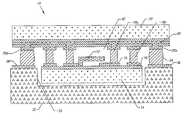
- FIG. 1is an enlarged cross-sectional view of one embodiment of the present invention
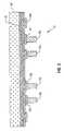
- FIG. 2is an enlarged cross-sectional view of a component of one embodiment of the present invention at an early stage of manufacturing
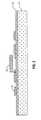
- FIG. 3is an enlarged cross-sectional view of another component of one embodiment of the present invention at an early stage of manufacture
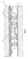
- FIG. 4is an enlarged cross-sectional view of the components shown in FIGS. 2 and 3 , having been joined, but still at an early stage of manufacturing;
- FIG. 5shows one technique for processing the structure shown in FIG. 4 in accordance with one embodiment of the present invention
- FIG. 6shows another technique for processing the component shown in FIG. 4 in accordance with one embodiment of the present invention.
- FIG. 7is an enlarged cross-sectional view of one embodiment after further processing.
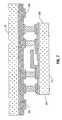
- a MEMS component 12such as a radio frequency (RF) MEMS component, including as examples a varactor, a switch or a resonator, may be formed on a semiconductor structure 14 having a layer 16 .
- a plurality of bond pads 15 and 16may be provided on the layer 16 .
- the MEMS component 12may be surrounded on one side by a printed circuit board 32 having a cavity 33 conforming to the shape of the semiconductor structure 14 in some embodiments. A gap may be maintained between the board 32 and the structure 14 .
- a plurality of solder bumps 34may bond the printed circuit board 32 to a semiconductor structure 22 through bond pads 36 and 20 a .
- the semiconductor structure 22may have internal electrical interconnection layers 40 that interconnect bond pads 15 , 20 a and 36 on the structure 14 , the board 32 and the semiconductor structure 22 . Thus, electrical connections are possible between the various components.
- a solder ring 18 bcompletely encircles the MEMS device 12 , defining a sealed or hermetic cavity 42 for the device 12 , in one embodiment. In another embodiment, the cavity 42 may be at a reduced pressure.
- the vias 18 aprovide electrical interconnections between the structure 14 and the structure 22 .
- the package 10may be processed by forming the MEMS device 12 on the structure 14 over a layer 16 as shown in FIG. 2 .
- a plurality of contacts 15may be provided as well.
- the layer 16may provide electrical connections between the contacts 15 and the MEMS device 12 through the semiconductor structure 14 in some embodiments.
- the semiconductor structure 22may include an internal electrical interconnection layer 40 that electrically couples pads 20 a and vias 18 a in one embodiment of the present invention.
- a sealing ring 18 bmay be coupled to a pad 20 , in accordance with one embodiment of the present invention.
- the sealing ring 18 bis not necessarily for electrical purposes but rather forms a vertical sealing wall between the structures 14 and 22 for hermetically sealing the MEMS device 12 inside the package 10 . Electrical interconnections to the outside would be provided by the vias 18 a coupled to the contacts 20 a , in one embodiment of the present invention.
- the contacts 20 amay be solder or gold bumps and the ring 18 b may be made of solder or gold, in some embodiments.
- the structures 14 and 22have been combined with the structure 22 positioned on top of the structure 14 .
- the combined package 10may be heated to fuse the vias 18 to the pads 15 and the ring 18 b to the bond ring 20 .
- surface mount techniquesusing temperatures of 300° C. or less may be used.
- a semiconductor wafer including a plurality of structures 14may be combined with a semiconductor wafer including a plurality of structures 22 .
- each pair of structures 14 and 22are simultaneously bonded to one another across the wafers.
- the solder ring 18 bmakes contact with bond ring 20 on the semiconductor structure 14 , forming a hermetic seal around the MEMS device 12 in the cavity 24 .
- the cavity 24may be a vacuum cavity.
- the electrical vias 18 aextend from the structure 22 to the structure 14 making electrical contact with the contacts 15 , in one embodiment of the present invention.
- electrical connectionsmay be made to and from the MEMS device 12 , circumventing the sealing ring 18 b via the buried interconnection layer 40 within the structure 22 in one embodiment.
- the ring 18 ais surface mounted to a pad 20 in turn coupled to the interconnection layer 40 which finally couples to a pad 20 a on the exterior of the sealing ring 18 b relative to the MEMS device 12 .
- the interconnection layer 40may be provided in either or both of the structures 14 and 22 in other embodiments.
- the structure shown in FIG. 4may be made at relatively low temperatures, for example under 300° C. in some embodiments, by using surface mounting techniques for combining the structures 14 and 22 .
- both of the structures 14 and 22may be severed along cut lines as indicated in FIG. 6 .
- a cut through the structure 22may be primarily to sever the structure 22 from the rest of its wafer.
- the cut through structure 14reveals bond pads 20 a on the structure 22 .
- a pair of electrical bond pads 20 amay be provided, but in another embodiment, any number of contacts 20 a may be utilized as necessary.
- FIG. 7After severing, in accordance with any of a variety of techniques including those shown in FIGS. 5 and 6 , the resulting structure is shown in FIG. 7 , with the pads 20 a fully accessible.
- a printed circuit board 32may be bonded to the semiconductor structure 22 . This may be done using solder bumps 34 and surface mount bonding pads 36 on the printed circuit board 32 to make electrical connection to the interconnection layers 40 through the bond pads 20 a .
- the structure 14may be left free floating for thermal compatibility or a suitable adhesive or filler may be used between the board 32 and the structure 14 .
Landscapes
- Engineering & Computer Science (AREA)
- Computer Hardware Design (AREA)
- Microelectronics & Electronic Packaging (AREA)
- Physics & Mathematics (AREA)
- Condensed Matter Physics & Semiconductors (AREA)
- General Physics & Mathematics (AREA)
- Power Engineering (AREA)
- Micromachines (AREA)
- Piezo-Electric Or Mechanical Vibrators, Or Delay Or Filter Circuits (AREA)
Abstract
Description
This invention relates generally to microelectromechanical structures (MEMS) and particularly to techniques for packaging MEMS.
In some cases, MEMS components such as varactors, switches and resonators need to be packaged in a hermetic environment. For example, particularly with radio frequency MEMS components, there may be a need for hermetic packaging. Such packaging protects the MEMS components from the outside environment.
Conventionally, two approaches have been utilized for hermetic packaging of MEMS components. Ceramic packages with cavities that may be sealed are used in the defense industry. This approach, while reliable, may be cost prohibitive for many commercial applications.
A second approach is to use a glass frit to bond a wafer containing the MEMS components to a cover. However, this technique requires high temperature bonding that may not be suitable for all components utilized in some MEMS applications. In some cases, the glass frit occupies a large area that increases the size of the resulting product and therefore increases its costs. In some cases, the glass frit bonding technology uses wire bonds for electrical connections that may not be adequate in some applications, such as high frequency applications.
Thus, there is a need for better ways to package MEMS components.
Referring toFIG. 1 , aMEMS component 12, such as a radio frequency (RF) MEMS component, including as examples a varactor, a switch or a resonator, may be formed on asemiconductor structure 14 having alayer 16. A plurality ofbond pads layer 16. TheMEMS component 12 may be surrounded on one side by a printedcircuit board 32 having acavity 33 conforming to the shape of thesemiconductor structure 14 in some embodiments. A gap may be maintained between theboard 32 and thestructure 14.
A plurality ofsolder bumps 34 may bond the printedcircuit board 32 to asemiconductor structure 22 throughbond pads semiconductor structure 22 may have internalelectrical interconnection layers 40 that interconnectbond pads structure 14, theboard 32 and thesemiconductor structure 22. Thus, electrical connections are possible between the various components.
Asolder ring 18bcompletely encircles theMEMS device 12, defining a sealed orhermetic cavity 42 for thedevice 12, in one embodiment. In another embodiment, thecavity 42 may be at a reduced pressure. Thevias 18aprovide electrical interconnections between thestructure 14 and thestructure 22.
In accordance with one embodiment of the present invention, thepackage 10 may be processed by forming theMEMS device 12 on thestructure 14 over alayer 16 as shown in FIG.2. In addition, a plurality ofcontacts 15 may be provided as well. Thelayer 16 may provide electrical connections between thecontacts 15 and theMEMS device 12 through thesemiconductor structure 14 in some embodiments.
Referring toFIG. 3 , thesemiconductor structure 22 may include an internalelectrical interconnection layer 40 that electrically couples pads20aand vias18ain one embodiment of the present invention. In addition, a sealingring 18bmay be coupled to apad 20, in accordance with one embodiment of the present invention. The sealingring 18bis not necessarily for electrical purposes but rather forms a vertical sealing wall between thestructures MEMS device 12 inside thepackage 10. Electrical interconnections to the outside would be provided by thevias 18acoupled to thecontacts 20a, in one embodiment of the present invention. Thecontacts 20amay be solder or gold bumps and thering 18bmay be made of solder or gold, in some embodiments.
Referring toFIG. 4 , thestructures structure 22 positioned on top of thestructure 14. The combinedpackage 10 may be heated to fuse the vias18 to thepads 15 and thering 18bto thebond ring 20. In some embodiments, surface mount techniques using temperatures of 300° C. or less may be used.
In one embodiment, a semiconductor wafer including a plurality ofstructures 14 may be combined with a semiconductor wafer including a plurality ofstructures 22. In that embodiment each pair ofstructures
At this stage, thesolder ring 18bmakes contact withbond ring 20 on thesemiconductor structure 14, forming a hermetic seal around theMEMS device 12 in thecavity 24. In some embodiments, thecavity 24 may be a vacuum cavity.
Theelectrical vias 18aextend from thestructure 22 to thestructure 14 making electrical contact with thecontacts 15, in one embodiment of the present invention. Thus, electrical connections may be made to and from theMEMS device 12, circumventing the sealingring 18bvia the buriedinterconnection layer 40 within thestructure 22 in one embodiment. For example, as shown inFIG. 4 , thering 18ais surface mounted to apad 20 in turn coupled to theinterconnection layer 40 which finally couples to apad 20aon the exterior of thesealing ring 18brelative to theMEMS device 12. However theinterconnection layer 40 may be provided in either or both of thestructures
In this way, electrical connections may be made to theMEMS device 12 through theexterior contacts 20a. In addition, the structure shown inFIG. 4 may be made at relatively low temperatures, for example under 300° C. in some embodiments, by using surface mounting techniques for combining thestructures
Referring toFIG. 5 , in accordance with one embodiment of the present invention, in order to access thecontacts 20a, lateral portions of thesemiconductor structure 14 may be cut away. In one embodiment, a thick saw, as indicated, may be utilized to saw through thesemiconductor structure 14 separating it from its wafer and a dicing saw may be utilized to separate thestructure 22 from the rest of its wafer.
In accordance with another embodiment, both of thestructures structure 22 may be primarily to sever thestructure 22 from the rest of its wafer. The cut throughstructure 14 revealsbond pads 20aon thestructure 22. In this case, a pair ofelectrical bond pads 20amay be provided, but in another embodiment, any number ofcontacts 20amay be utilized as necessary.
Again, theinterconnection layer 40 acts as a buried contact to allow electrical connections from theMEMS device 12 in the interior of thecavity 24 to the outside world without compromising the sealed nature of thecavity 24.
After severing, in accordance with any of a variety of techniques including those shown inFIGS. 5 and 6 , the resulting structure is shown inFIG. 7 , with thepads 20afully accessible.
Next, as shown inFIG. 1 , aprinted circuit board 32 may be bonded to thesemiconductor structure 22. This may be done usingsolder bumps 34 and surfacemount bonding pads 36 on the printedcircuit board 32 to make electrical connection to theinterconnection layers 40 through thebond pads 20a. Thestructure 14 may be left free floating for thermal compatibility or a suitable adhesive or filler may be used between theboard 32 and thestructure 14.
Again, by using surface mount techniques, the processing temperatures may be reduced. Lower processing temperatures may be important in processing MEMS components in some embodiments.
While the present invention has been described with respect to a limited number of embodiments, those skilled in the art will appreciate numerous modifications and variations therefrom. It is intended that the appended claims cover all such modifications and variations as fall within the true spirit and scope of this present invention.
Claims (18)
1. A packaged microelectromechanical structure device comprising:
a first semiconductor structure;
a microelectromechanical structure device formed on the first semiconductor structure;
a second semiconductor structure;
a vertical wall extending between said first and second structures around said device to form a hermetic cavity enclosing said device between said first and second structures; and
a printed circuit board bonded to said second semiconductor structure around said first semiconductor structure.
2. The device ofclaim 1 wherein said wall is secured to said first and second structures by bonding pads and wherein said wall is formed of a material that is surface mountable.
3. The device ofclaim 1 including an electrical contact in said cavity to make contact to said microelectromechanical structure device, an interconnection layer extending through one of said first and second structures, and an electrical contact on the exterior of said cavity on one of said first and second structures to enable an electrical connection to be made to said microelectromechanical structure device from the exterior of said cavity.
4. The device ofclaim 3 wherein said interconnection layer is in said second semiconductor structure.
5. The device ofclaim 4 including a via that extends from said first semiconductor structure to said second semiconductor structure coupling said contact to said interconnection layer.
6. The device ofclaim 3 wherein said interconnection layer extends through the interior of said second semiconductor structure.
7. The device ofclaim 1 wherein said board is surface mounted to said second semiconductor structure.
8. The device ofclaim 7 wherein the board does not directly connect to said first semiconductor structure.
9. The device ofclaim 8 wherein said first semiconductor structure is smaller than said second semiconductor structure.
10. A packaged microelectromechanical structure device comprising:
a first semiconductor structure;
a microelectromechanical structure device formed on said first semiconductor structure;
a second semiconductor structure bonded to said first semiconductor structure to farm a hermetic cavity surrounding said device;
an interconnection layer through one of said first and second semiconductor structures to enable electrical connections from outside said cavity to said device within said cavity; and
a printed circuit board bonded to said second semiconductor structure around said first semiconductor structure.
11. The device ofclaim 10 wherein said interconnection layer extends through said second semiconductor structure.
12. The device ofclaim 10 including a vertical wall extending between said first and second structures to form said hermetic cavity.
13. The device ofclaim 12 including bonding pads on said first and second structures, said vertical wall contacting said bonding pads.
14. The device ofclaim 10 wherein said first and second semiconductor structures are surface mounted to one another.
15. The device ofclaim 10 wherein said board is surface mounted to said second semiconductor structure.
16. The device ofclaim 15 wherein said board does not directly connect to said first semiconductor structure.
17. The device ofclaim 16 wherein said first semiconductor structure is smaller than said second semiconductor structure.
18. The device ofclaim 10 wherein said interconnection layer extends through the interior of said second semiconductor structure.
Priority Applications (6)
| Application Number | Priority Date | Filing Date | Title |
|---|---|---|---|
| US10/106,728US6852926B2 (en) | 2002-03-26 | 2002-03-26 | Packaging microelectromechanical structures |
| AU2003212969AAU2003212969A1 (en) | 2002-03-26 | 2003-02-07 | Packaging microelectromechanical structures |
| PCT/US2003/003798WO2003083883A2 (en) | 2002-03-26 | 2003-02-07 | Packaging microelectromechanical structures |
| TW092102789ATW588421B (en) | 2002-03-26 | 2003-02-11 | Packaging microelectromechanical structures |
| MYPI20030546AMY138751A (en) | 2002-03-26 | 2003-02-18 | Packaging microelectromechanical structures |
| US10/980,516US20050062120A1 (en) | 2002-03-26 | 2004-11-03 | Packaging microelectromechanical structures |
Applications Claiming Priority (1)
| Application Number | Priority Date | Filing Date | Title |
|---|---|---|---|
| US10/106,728US6852926B2 (en) | 2002-03-26 | 2002-03-26 | Packaging microelectromechanical structures |
Related Child Applications (1)
| Application Number | Title | Priority Date | Filing Date |
|---|---|---|---|
| US10/980,516DivisionUS20050062120A1 (en) | 2002-03-26 | 2004-11-03 | Packaging microelectromechanical structures |
Publications (2)
| Publication Number | Publication Date |
|---|---|
| US20030183407A1 US20030183407A1 (en) | 2003-10-02 |
| US6852926B2true US6852926B2 (en) | 2005-02-08 |
Family
ID=28452551
Family Applications (2)
| Application Number | Title | Priority Date | Filing Date |
|---|---|---|---|
| US10/106,728Expired - LifetimeUS6852926B2 (en) | 2002-03-26 | 2002-03-26 | Packaging microelectromechanical structures |
| US10/980,516AbandonedUS20050062120A1 (en) | 2002-03-26 | 2004-11-03 | Packaging microelectromechanical structures |
Family Applications After (1)
| Application Number | Title | Priority Date | Filing Date |
|---|---|---|---|
| US10/980,516AbandonedUS20050062120A1 (en) | 2002-03-26 | 2004-11-03 | Packaging microelectromechanical structures |
Country Status (5)
| Country | Link |
|---|---|
| US (2) | US6852926B2 (en) |
| AU (1) | AU2003212969A1 (en) |
| MY (1) | MY138751A (en) |
| TW (1) | TW588421B (en) |
| WO (1) | WO2003083883A2 (en) |
Cited By (43)
| Publication number | Priority date | Publication date | Assignee | Title |
|---|---|---|---|---|
| US20040264152A1 (en)* | 2003-06-25 | 2004-12-30 | Heck John M. | MEMS RF switch module including a vertical via |
| US20050012169A1 (en)* | 2003-06-06 | 2005-01-20 | Sanyo Electric Co., Ltd. | Semiconductor device and manufacturing method of the same |
| US20050127499A1 (en)* | 2003-12-15 | 2005-06-16 | Harney Kieran P. | Mems device with conductive path through substrate |
| US20050146004A1 (en)* | 2003-12-16 | 2005-07-07 | Masami Seto | Semiconductor sensor device and method of producing the same |
| US20050170609A1 (en)* | 2003-12-15 | 2005-08-04 | Alie Susan A. | Conductive bond for through-wafer interconnect |
| US20050241850A1 (en)* | 2004-04-29 | 2005-11-03 | International Business Machines Corporation | Method and structures for implementing customizable dielectric printed circuit card traces |
| US20060001123A1 (en)* | 2004-06-30 | 2006-01-05 | John Heck | Module integrating MEMS and passive components |
| US20060166480A1 (en)* | 2004-06-02 | 2006-07-27 | Analog Devices, Inc. | Interconnection of through-wafer vias using bridge structures |
| US20060208326A1 (en)* | 2005-03-18 | 2006-09-21 | Nasiri Steven S | Method of fabrication of ai/ge bonding in a wafer packaging environment and a product produced therefrom |
| US20060238951A1 (en)* | 2002-12-31 | 2006-10-26 | The Regents Of The University Of California | MEMS Fabrication on a Laminated substrate |
| US20070000976A1 (en)* | 2005-06-30 | 2007-01-04 | Arana Leonel R | Electrically-isolated interconnects and seal rings in packages using a solder preform |
| US20070077747A1 (en)* | 2005-09-30 | 2007-04-05 | John Heck | Microelectronic package having multiple conductive paths through an opening in a support substrate |
| US20070200222A1 (en)* | 2006-02-27 | 2007-08-30 | Texas Instruments Incorporated | Semiconductor device and method of fabrication |
| US20070235501A1 (en)* | 2006-03-29 | 2007-10-11 | John Heck | Self-packaging MEMS device |
| US20070269926A1 (en)* | 2006-05-16 | 2007-11-22 | Schultz Peter S | Method and apparatus for forming an electrical connection to a semiconductor substrate |
| US20080087979A1 (en)* | 2006-10-13 | 2008-04-17 | Analog Devices, Inc. | Integrated Circuit with Back Side Conductive Paths |
| US20080282802A1 (en)* | 2002-01-25 | 2008-11-20 | Pike William T | Fabrication process and package design for use in a micro-machined seismometer or other device |
| US20090098685A1 (en)* | 2005-04-05 | 2009-04-16 | Texas Instruments Incorporated | Low Cost Hermetically Sealed Package |
| US20090127639A1 (en)* | 2007-09-21 | 2009-05-21 | Kabushiki Kaisha Toshiba | Semiconductor apparatus |
| US20090146229A1 (en)* | 2007-12-10 | 2009-06-11 | Eun-Soo Jeong | Semiconductor device and method for fabricating the same |
| US20090173936A1 (en)* | 2008-01-03 | 2009-07-09 | Bunyk Paul I | Quantum processor |
| US20090194861A1 (en)* | 2008-02-04 | 2009-08-06 | Mathias Bonse | Hermetically-packaged devices, and methods for hermetically packaging at least one device at the wafer level |
| US20090261691A1 (en)* | 2006-08-25 | 2009-10-22 | Kyocera Corporation | Microelectromechanical device and method for manufacturing the same |
| US20100237489A1 (en)* | 2009-03-17 | 2010-09-23 | Texas Instruments Incorporated | Structure and Method for Sealing Cavity of Micro-Electro-Mechanical Device |
| US20110059567A1 (en)* | 2009-09-04 | 2011-03-10 | Magic Technologies, Inc. | MEMS device package with vacuum cavity by two-step solder reflow method |
| US20110236384A1 (en)* | 2005-06-24 | 2011-09-29 | Duke University | Direct drug delivery system based on thermally responsive biopolymers |
| US20120267732A1 (en)* | 2009-08-11 | 2012-10-25 | Pixart Imaging Inc. | Mems package structure |
| US8567246B2 (en) | 2010-10-12 | 2013-10-29 | Invensense, Inc. | Integrated MEMS device and method of use |
| US20140070900A1 (en)* | 2012-09-11 | 2014-03-13 | Seiko Epson Corporation | Electronic device, method of manufacturing the same, and oscillator |
| US8860409B2 (en) | 2011-01-11 | 2014-10-14 | Invensense, Inc. | Micromachined resonant magnetic field sensors |
| US8947081B2 (en) | 2011-01-11 | 2015-02-03 | Invensense, Inc. | Micromachined resonant magnetic field sensors |
| US9162874B2 (en)* | 2014-01-22 | 2015-10-20 | Taiwan Semiconductor Manufacturing Company Ltd. | Semiconductor structure and method forming the same |
| US9493341B2 (en) | 2010-06-25 | 2016-11-15 | International Business Machines Corporation | Planar cavity MEMS and related structures, methods of manufacture and design structures |
| US9664750B2 (en) | 2011-01-11 | 2017-05-30 | Invensense, Inc. | In-plane sensing Lorentz force magnetometer |
| US9754922B2 (en) | 2015-02-11 | 2017-09-05 | Invensense, Inc. | 3D integration using Al—Ge eutectic bond interconnect |
| US9764946B2 (en) | 2013-10-24 | 2017-09-19 | Analog Devices, Inc. | MEMs device with outgassing shield |
| US10192850B1 (en) | 2016-09-19 | 2019-01-29 | Sitime Corporation | Bonding process with inhibited oxide formation |
| US10769546B1 (en)* | 2015-04-27 | 2020-09-08 | Rigetti & Co, Inc. | Microwave integrated quantum circuits with cap wafer and methods for making the same |
| US11121301B1 (en) | 2017-06-19 | 2021-09-14 | Rigetti & Co, Inc. | Microwave integrated quantum circuits with cap wafers and their methods of manufacture |
| US11617272B2 (en) | 2016-12-07 | 2023-03-28 | D-Wave Systems Inc. | Superconducting printed circuit board related systems, methods, and apparatus |
| US11647590B2 (en) | 2019-06-18 | 2023-05-09 | D-Wave Systems Inc. | Systems and methods for etching of metals |
| US11678433B2 (en) | 2018-09-06 | 2023-06-13 | D-Wave Systems Inc. | Printed circuit board assembly for edge-coupling to an integrated circuit |
| US12033996B2 (en) | 2019-09-23 | 2024-07-09 | 1372934 B.C. Ltd. | Systems and methods for assembling processor systems |
Families Citing this family (20)
| Publication number | Priority date | Publication date | Assignee | Title |
|---|---|---|---|---|
| TW569407B (en)* | 2002-05-17 | 2004-01-01 | Advanced Semiconductor Eng | Wafer-level package with bump and method for manufacturing the same |
| US20070102831A1 (en)* | 2003-12-24 | 2007-05-10 | Shuntaro Machida | Device and method of manufacturing the same |
| US7422962B2 (en)* | 2004-10-27 | 2008-09-09 | Hewlett-Packard Development Company, L.P. | Method of singulating electronic devices |
| JP2007059470A (en)* | 2005-08-22 | 2007-03-08 | Sony Corp | Semiconductor device and manufacturing method thereof |
| US7968364B2 (en)* | 2005-10-03 | 2011-06-28 | Analog Devices, Inc. | MEMS switch capping and passivation method |
| US20070114643A1 (en)* | 2005-11-22 | 2007-05-24 | Honeywell International Inc. | Mems flip-chip packaging |
| CN101421178B (en)* | 2006-04-13 | 2012-11-07 | 盛投资有限责任公司 | A method for manufacturing an electronic assembly, electronic assembly, covering piece and substrate |
| KR100772321B1 (en)* | 2006-06-14 | 2007-10-31 | 매그나칩 반도체 유한회사 | Package of MEMS element and manufacturing method thereof |
| US20080283065A1 (en)* | 2007-05-15 | 2008-11-20 | Portaero, Inc. | Methods and devices to maintain patency of a lumen in parenchymal tissue of the lung |
| EP2011762B1 (en)* | 2007-07-02 | 2015-09-30 | Denso Corporation | Semiconductor device with a sensor connected to an external element |
| DE102007044806A1 (en)* | 2007-09-20 | 2009-04-02 | Robert Bosch Gmbh | Micromechanical component and method for producing a micromechanical component |
| CN101837944B (en)* | 2008-11-19 | 2012-06-13 | 明锐有限公司 | Method for forming a gyroscope and accelerometer |
| JP4858547B2 (en)* | 2009-01-09 | 2012-01-18 | 株式会社デンソー | Semiconductor device and manufacturing method thereof |
| US8296940B2 (en)* | 2010-04-19 | 2012-10-30 | General Electric Company | Method of forming a micro pin hybrid interconnect array |
| CN102649536A (en)* | 2011-02-25 | 2012-08-29 | 永春至善体育用品有限公司 | Structure-enhancing and sensitivity-increasing method for micro-machined components |
| JP5605347B2 (en)* | 2011-11-01 | 2014-10-15 | 株式会社デンソー | Manufacturing method of semiconductor device |
| US11257774B2 (en)* | 2014-08-31 | 2022-02-22 | Skyworks Solutions, Inc. | Stack structures in electronic devices including passivation layers for distributing compressive force |
| JP6702019B2 (en)* | 2016-06-22 | 2020-05-27 | 株式会社ジェイテクト | Semiconductor device |
| CN111392683B (en)* | 2020-02-28 | 2024-03-15 | 上海集成电路研发中心有限公司 | Infrared detector structure and manufacturing method |
| CN114188313B (en)* | 2020-09-15 | 2024-11-05 | 江苏中科智芯集成科技有限公司 | Wafer-level packaging structure and packaging method thereof |
Citations (9)
| Publication number | Priority date | Publication date | Assignee | Title |
|---|---|---|---|---|
| US5610431A (en) | 1995-05-12 | 1997-03-11 | The Charles Stark Draper Laboratory, Inc. | Covers for micromechanical sensors and other semiconductor devices |
| WO1998006118A1 (en) | 1996-08-05 | 1998-02-12 | Mcnc | Encapsulated micro-relay modules and methods of fabricating same |
| US6219254B1 (en) | 1999-04-05 | 2001-04-17 | Trw Inc. | Chip-to-board connection assembly and method therefor |
| US6297072B1 (en)* | 1998-04-17 | 2001-10-02 | Interuniversitair Micro-Elktronica Centrum (Imec Vzw) | Method of fabrication of a microstructure having an internal cavity |
| US20020000646A1 (en) | 2000-02-02 | 2002-01-03 | Raytheon Company, A Delware Corporation | Vacuum package fabrication of integrated circuit components |
| US6528344B2 (en)* | 2000-06-22 | 2003-03-04 | Samsung Electronics Co., Ltd. | Chip scale surface-mountable packaging method for electronic and MEMS devices |
| US6550664B2 (en)* | 2000-12-09 | 2003-04-22 | Agilent Technologies, Inc. | Mounting film bulk acoustic resonators in microwave packages using flip chip bonding technology |
| US6596117B2 (en)* | 1998-07-10 | 2003-07-22 | Drs Sensors & Targeting Systems, Inc. | Method for fabricating a sealed-cavity microstructure |
| US6624003B1 (en)* | 2002-02-06 | 2003-09-23 | Teravicta Technologies, Inc. | Integrated MEMS device and package |
Family Cites Families (1)
| Publication number | Priority date | Publication date | Assignee | Title |
|---|---|---|---|---|
| US20020096421A1 (en)* | 2000-11-29 | 2002-07-25 | Cohn Michael B. | MEMS device with integral packaging |
- 2002
- 2002-03-26USUS10/106,728patent/US6852926B2/ennot_activeExpired - Lifetime
- 2003
- 2003-02-07AUAU2003212969Apatent/AU2003212969A1/ennot_activeAbandoned
- 2003-02-07WOPCT/US2003/003798patent/WO2003083883A2/ennot_activeApplication Discontinuation
- 2003-02-11TWTW092102789Apatent/TW588421B/ennot_activeIP Right Cessation
- 2003-02-18MYMYPI20030546Apatent/MY138751A/enunknown
- 2004
- 2004-11-03USUS10/980,516patent/US20050062120A1/ennot_activeAbandoned
Patent Citations (9)
| Publication number | Priority date | Publication date | Assignee | Title |
|---|---|---|---|---|
| US5610431A (en) | 1995-05-12 | 1997-03-11 | The Charles Stark Draper Laboratory, Inc. | Covers for micromechanical sensors and other semiconductor devices |
| WO1998006118A1 (en) | 1996-08-05 | 1998-02-12 | Mcnc | Encapsulated micro-relay modules and methods of fabricating same |
| US6297072B1 (en)* | 1998-04-17 | 2001-10-02 | Interuniversitair Micro-Elktronica Centrum (Imec Vzw) | Method of fabrication of a microstructure having an internal cavity |
| US6596117B2 (en)* | 1998-07-10 | 2003-07-22 | Drs Sensors & Targeting Systems, Inc. | Method for fabricating a sealed-cavity microstructure |
| US6219254B1 (en) | 1999-04-05 | 2001-04-17 | Trw Inc. | Chip-to-board connection assembly and method therefor |
| US20020000646A1 (en) | 2000-02-02 | 2002-01-03 | Raytheon Company, A Delware Corporation | Vacuum package fabrication of integrated circuit components |
| US6528344B2 (en)* | 2000-06-22 | 2003-03-04 | Samsung Electronics Co., Ltd. | Chip scale surface-mountable packaging method for electronic and MEMS devices |
| US6550664B2 (en)* | 2000-12-09 | 2003-04-22 | Agilent Technologies, Inc. | Mounting film bulk acoustic resonators in microwave packages using flip chip bonding technology |
| US6624003B1 (en)* | 2002-02-06 | 2003-09-23 | Teravicta Technologies, Inc. | Integrated MEMS device and package |
Non-Patent Citations (3)
| Title |
|---|
| H. Tilmans et al., The Indent Reflow Sealing (IRS) Technique-A Method for the Fabrication of Sealed Cavities for MEMS Devices, Journal of Microelectromechanical Systems, IEEE, New York, USA, vol. 9, No. 2, Jun. 2000, pp. 206-217. |
| J. Neysmith et al., A Modular, Direct-Chip-Attach Package: Architecture and Processing, 2000 International Symposium on Microelectronic, Boston, MA, Sep. 2000, pp. 569-573. |
| S. Renard, Wafer level Surface Mountable Chip Size Paging for MEMS and ICs, Proceedings of the SPIE, Bellingham, VA, vol. 4176, Sep. 2000, pp. 236-291. |
Cited By (119)
| Publication number | Priority date | Publication date | Assignee | Title |
|---|---|---|---|---|
| US9869796B2 (en) | 2002-01-25 | 2018-01-16 | Kinemetrics, Inc. | Fabrication process and package design for use in a micro-machined seismometer or other device |
| US20110170376A1 (en)* | 2002-01-25 | 2011-07-14 | Pike William T | Fabrication process and package design for use in a micro-machined seismometer or other device |
| US8978246B2 (en)* | 2002-01-25 | 2015-03-17 | Kinemetrics, Inc. | Fabrication process and package design for use in a micro-machined seismometer or other device |
| US20080282802A1 (en)* | 2002-01-25 | 2008-11-20 | Pike William T | Fabrication process and package design for use in a micro-machined seismometer or other device |
| US7870788B2 (en) | 2002-01-25 | 2011-01-18 | Kinemetrics, Inc. | Fabrication process and package design for use in a micro-machined seismometer or other device |
| US20060238951A1 (en)* | 2002-12-31 | 2006-10-26 | The Regents Of The University Of California | MEMS Fabrication on a Laminated substrate |
| US7884689B2 (en)* | 2002-12-31 | 2011-02-08 | The Regents Of The University Of California | MEMS fabrication on a laminated substrate |
| US20050012169A1 (en)* | 2003-06-06 | 2005-01-20 | Sanyo Electric Co., Ltd. | Semiconductor device and manufacturing method of the same |
| US20070096294A1 (en)* | 2003-06-06 | 2007-05-03 | Sanyo Electric Co., Ltd. | Semiconductor device and manufacturing method of the same |
| US7154173B2 (en)* | 2003-06-06 | 2006-12-26 | Sanyo Electric Co., Ltd. | Semiconductor device and manufacturing method of the same |
| US7170155B2 (en)* | 2003-06-25 | 2007-01-30 | Intel Corporation | MEMS RF switch module including a vertical via |
| US20040264152A1 (en)* | 2003-06-25 | 2004-12-30 | Heck John M. | MEMS RF switch module including a vertical via |
| US20070029659A1 (en)* | 2003-06-25 | 2007-02-08 | Heck John M | MEMS RF switch module including a vertical via |
| US7324350B2 (en) | 2003-06-25 | 2008-01-29 | Intel Corporation | MEMS RF switch module including a vertical via |
| US6936918B2 (en)* | 2003-12-15 | 2005-08-30 | Analog Devices, Inc. | MEMS device with conductive path through substrate |
| US20050170609A1 (en)* | 2003-12-15 | 2005-08-04 | Alie Susan A. | Conductive bond for through-wafer interconnect |
| US20050127499A1 (en)* | 2003-12-15 | 2005-06-16 | Harney Kieran P. | Mems device with conductive path through substrate |
| US20050146004A1 (en)* | 2003-12-16 | 2005-07-07 | Masami Seto | Semiconductor sensor device and method of producing the same |
| US7129417B2 (en)* | 2004-04-29 | 2006-10-31 | International Business Machines Corporation | Method and structures for implementing customizable dielectric printed circuit card traces |
| US20050241850A1 (en)* | 2004-04-29 | 2005-11-03 | International Business Machines Corporation | Method and structures for implementing customizable dielectric printed circuit card traces |
| US20060288570A1 (en)* | 2004-04-29 | 2006-12-28 | International Business Machines Corporation | Method and structures for implementing customizable dielectric printed circuit card traces |
| US7197818B2 (en) | 2004-04-29 | 2007-04-03 | International Business Machines Corporation | Method and structures for implementing customizable dielectric printed circuit card traces |
| US20060166480A1 (en)* | 2004-06-02 | 2006-07-27 | Analog Devices, Inc. | Interconnection of through-wafer vias using bridge structures |
| US7608534B2 (en) | 2004-06-02 | 2009-10-27 | Analog Devices, Inc. | Interconnection of through-wafer vias using bridge structures |
| US7183622B2 (en)* | 2004-06-30 | 2007-02-27 | Intel Corporation | Module integrating MEMS and passive components |
| US20060001123A1 (en)* | 2004-06-30 | 2006-01-05 | John Heck | Module integrating MEMS and passive components |
| US8633049B2 (en) | 2005-03-18 | 2014-01-21 | Invensense, Inc. | Method of fabrication of Al/GE bonding in a wafer packaging environment and a product produced therefrom |
| US8084332B2 (en) | 2005-03-18 | 2011-12-27 | Invensense, Inc. | Method of fabrication of AI/GE bonding in a wafer packaging environment and a product produced therefrom |
| US9751752B2 (en) | 2005-03-18 | 2017-09-05 | Invensense, Inc. | Method of fabrication of Al/Ge bonding in a wafer packaging environment and a product produced therefrom |
| US9139428B2 (en) | 2005-03-18 | 2015-09-22 | Invensense, Inc. | Method of fabrication of Al/Ge bonding in a wafer packaging environment and a product produced therefrom |
| US7442570B2 (en) | 2005-03-18 | 2008-10-28 | Invensence Inc. | Method of fabrication of a AL/GE bonding in a wafer packaging environment and a product produced therefrom |
| US20060208326A1 (en)* | 2005-03-18 | 2006-09-21 | Nasiri Steven S | Method of fabrication of ai/ge bonding in a wafer packaging environment and a product produced therefrom |
| US20090098685A1 (en)* | 2005-04-05 | 2009-04-16 | Texas Instruments Incorporated | Low Cost Hermetically Sealed Package |
| US8778741B2 (en)* | 2005-04-05 | 2014-07-15 | Texas Instruments Incorporated | Low cost hermetically sealed package |
| US20110236384A1 (en)* | 2005-06-24 | 2011-09-29 | Duke University | Direct drug delivery system based on thermally responsive biopolymers |
| US7243833B2 (en) | 2005-06-30 | 2007-07-17 | Intel Corporation | Electrically-isolated interconnects and seal rings in packages using a solder preform |
| US20070000976A1 (en)* | 2005-06-30 | 2007-01-04 | Arana Leonel R | Electrically-isolated interconnects and seal rings in packages using a solder preform |
| US20070077747A1 (en)* | 2005-09-30 | 2007-04-05 | John Heck | Microelectronic package having multiple conductive paths through an opening in a support substrate |
| US7358615B2 (en) | 2005-09-30 | 2008-04-15 | Intel Corporation | Microelectronic package having multiple conductive paths through an opening in a support substrate |
| US7449765B2 (en)* | 2006-02-27 | 2008-11-11 | Texas Instruments Incorporated | Semiconductor device and method of fabrication |
| US20070200222A1 (en)* | 2006-02-27 | 2007-08-30 | Texas Instruments Incorporated | Semiconductor device and method of fabrication |
| US20070235501A1 (en)* | 2006-03-29 | 2007-10-11 | John Heck | Self-packaging MEMS device |
| US7524693B2 (en)* | 2006-05-16 | 2009-04-28 | Freescale Semiconductor, Inc. | Method and apparatus for forming an electrical connection to a semiconductor substrate |
| US20070269926A1 (en)* | 2006-05-16 | 2007-11-22 | Schultz Peter S | Method and apparatus for forming an electrical connection to a semiconductor substrate |
| US20090261691A1 (en)* | 2006-08-25 | 2009-10-22 | Kyocera Corporation | Microelectromechanical device and method for manufacturing the same |
| US8159059B2 (en)* | 2006-08-25 | 2012-04-17 | Kyocera Corporation | Microelectromechanical device and method for manufacturing the same |
| US20080087979A1 (en)* | 2006-10-13 | 2008-04-17 | Analog Devices, Inc. | Integrated Circuit with Back Side Conductive Paths |
| US20090127639A1 (en)* | 2007-09-21 | 2009-05-21 | Kabushiki Kaisha Toshiba | Semiconductor apparatus |
| US7973374B2 (en) | 2007-12-10 | 2011-07-05 | Dongbu Hitek Co., Ltd. | Semiconductor device and method for fabricating the same |
| DE102008061151B4 (en)* | 2007-12-10 | 2011-12-01 | Dongbu Hitek Co., Ltd. | Semiconductor component and method for its production |
| US20090146229A1 (en)* | 2007-12-10 | 2009-06-11 | Eun-Soo Jeong | Semiconductor device and method for fabricating the same |
| US7932515B2 (en) | 2008-01-03 | 2011-04-26 | D-Wave Systems Inc. | Quantum processor |
| US20090173936A1 (en)* | 2008-01-03 | 2009-07-09 | Bunyk Paul I | Quantum processor |
| US20090194861A1 (en)* | 2008-02-04 | 2009-08-06 | Mathias Bonse | Hermetically-packaged devices, and methods for hermetically packaging at least one device at the wafer level |
| US7919842B2 (en)* | 2009-03-17 | 2011-04-05 | Texas Instruments Incorporated | Structure and method for sealing cavity of micro-electro-mechanical device |
| US20100237489A1 (en)* | 2009-03-17 | 2010-09-23 | Texas Instruments Incorporated | Structure and Method for Sealing Cavity of Micro-Electro-Mechanical Device |
| US20120267732A1 (en)* | 2009-08-11 | 2012-10-25 | Pixart Imaging Inc. | Mems package structure |
| US8829628B2 (en)* | 2009-08-11 | 2014-09-09 | Pixart Imaging Inc. | MEMS package structure |
| US8058106B2 (en) | 2009-09-04 | 2011-11-15 | Magic Technologies, Inc. | MEMS device package with vacuum cavity by two-step solder reflow method |
| US20110059567A1 (en)* | 2009-09-04 | 2011-03-10 | Magic Technologies, Inc. | MEMS device package with vacuum cavity by two-step solder reflow method |
| US10246319B2 (en) | 2010-06-25 | 2019-04-02 | International Business Machines Corporation | Planar cavity MEMS and related structures, methods of manufacture and design structures |
| US10315913B2 (en) | 2010-06-25 | 2019-06-11 | International Business Machines Corporation | Planar cavity MEMS and related structures, methods of manufacture and design structures |
| US11174160B2 (en) | 2010-06-25 | 2021-11-16 | International Business Machines Corporation | Planar cavity MEMS and related structures, methods of manufacture and design structures |
| US11111138B2 (en) | 2010-06-25 | 2021-09-07 | International Business Machines Corporation | Planar cavity mems and related structures, methods of manufacture and design structures |
| US9493341B2 (en) | 2010-06-25 | 2016-11-15 | International Business Machines Corporation | Planar cavity MEMS and related structures, methods of manufacture and design structures |
| US9493343B2 (en) | 2010-06-25 | 2016-11-15 | International Business Machines Corporation | Planar cavity MEMS and related structures, methods of manufacture and design structures |
| US9624099B2 (en) | 2010-06-25 | 2017-04-18 | International Business Machines Corporation | Planar cavity MEMS and related structures, methods of manufacture and design structures |
| US9637373B2 (en) | 2010-06-25 | 2017-05-02 | International Business Machines Corporation | Planar cavity MEMS and related structures, methods of manufacture and design structures |
| US11111139B2 (en) | 2010-06-25 | 2021-09-07 | International Business Machines Corporation | Planar cavity MEMS and related structures, methods of manufacture and design structures |
| US11104572B2 (en) | 2010-06-25 | 2021-08-31 | International Business Machines Corporation | Planar cavity MEMS and related structures, methods of manufacture and design structures |
| US11021364B2 (en) | 2010-06-25 | 2021-06-01 | International Business Machines Corporation | Planar cavity MEMS and related structures, methods of manufacture and design structures |
| US9764944B2 (en) | 2010-06-25 | 2017-09-19 | International Business Machines Corporation | Planar cavity MEMS and related structures, methods of manufacture and design structures |
| US10906803B2 (en) | 2010-06-25 | 2021-02-02 | International Business Machines Corporation | Planar cavity MEMS and related structures, methods of manufacture and design structures |
| US9815690B2 (en) | 2010-06-25 | 2017-11-14 | International Business Machines Corporation | Planar cavity MEMS and related structures, methods of manufacture and design structures |
| US9828243B2 (en)* | 2010-06-25 | 2017-11-28 | International Business Machines Corporation | Planar cavity MEMS and related structures, methods of manufacture and design structures |
| US9862598B2 (en) | 2010-06-25 | 2018-01-09 | International Business Machines Corporation | Planar cavity MEMS and related structures, methods of manufacture and design structures |
| US10766765B2 (en) | 2010-06-25 | 2020-09-08 | International Business Machines Corporation | Planar cavity MEMS and related structures, methods of manufacture and design structures |
| US9890039B2 (en) | 2010-06-25 | 2018-02-13 | International Business Machines Corporation | Planar cavity MEMS and related structures, methods of manufacture and design structures |
| US9926191B2 (en) | 2010-06-25 | 2018-03-27 | International Business Machines Corporation | Planar cavity MEMS and related structures, methods of manufacture and design structures |
| US9932225B2 (en) | 2010-06-25 | 2018-04-03 | International Business Machines Corporation | Planar cavity MEMS and related structures, methods of manufacture and design structures |
| US10005661B2 (en) | 2010-06-25 | 2018-06-26 | International Business Machines Corporation | Planar cavity MEMS and related structures, methods of manufacture and design structures |
| US10011480B2 (en) | 2010-06-25 | 2018-07-03 | International Business Machines Corporation | Planar cavity MEMS and related structures, methods of manufacture and design structures |
| US10011477B2 (en) | 2010-06-25 | 2018-07-03 | International Business Machines Corporation | Planar cavity MEMS and related structures, methods of manufacture and design structures |
| US10081540B2 (en) | 2010-06-25 | 2018-09-25 | International Business Machines Corporation | Planar cavity MEMS and related structures, methods of manufacture and design structures |
| US10093537B2 (en) | 2010-06-25 | 2018-10-09 | International Business Machines Corporation | Planar cavity MEMS and related structures, methods of manufacture and design structures |
| US10173889B2 (en) | 2010-06-25 | 2019-01-08 | Globalfoundries Inc. | Planar cavity MEMS and related structures, methods of manufacture and design structures |
| US10640364B2 (en) | 2010-06-25 | 2020-05-05 | International Business Machines Corporation | Planar cavity MEMS and related structures, methods of manufacture and design structures |
| US10214416B2 (en) | 2010-06-25 | 2019-02-26 | International Business Machines Corporation | Planar cavity MEMS and related structures, methods of manufacture and design structures |
| US10640365B2 (en) | 2010-06-25 | 2020-05-05 | International Business Machines Corporation | Planar cavity MEMS and related structures, methods of manufacture and design structures |
| US10308501B2 (en) | 2010-06-25 | 2019-06-04 | International Business Machines Corporation | Planar cavity MEMS and related structures, methods of manufacture and design structures |
| US10618803B2 (en) | 2010-06-25 | 2020-04-14 | International Business Machines Corporation | Planar cavity MEMS and related structures, methods of manufacture and design structures |
| US10414646B2 (en) | 2010-06-25 | 2019-09-17 | International Business Machines Corporation | Planar cavity MEMS and related structures, methods of manufacture and design structures |
| US10618802B2 (en) | 2010-06-25 | 2020-04-14 | International Business Machines Corporation | Planar cavity MEMS and related structures, methods of manufacture and design structures |
| US10584026B2 (en) | 2010-06-25 | 2020-03-10 | International Business Machines Corporation | Planar cavity MEMS and related structures, methods of manufacture and design structures |
| US8567246B2 (en) | 2010-10-12 | 2013-10-29 | Invensense, Inc. | Integrated MEMS device and method of use |
| US8947081B2 (en) | 2011-01-11 | 2015-02-03 | Invensense, Inc. | Micromachined resonant magnetic field sensors |
| US9664750B2 (en) | 2011-01-11 | 2017-05-30 | Invensense, Inc. | In-plane sensing Lorentz force magnetometer |
| US8860409B2 (en) | 2011-01-11 | 2014-10-14 | Invensense, Inc. | Micromachined resonant magnetic field sensors |
| US9089055B2 (en)* | 2012-09-11 | 2015-07-21 | Seiko Epson Corporation | Electronic device, method of manufacturing the same, and oscillator |
| US20140070900A1 (en)* | 2012-09-11 | 2014-03-13 | Seiko Epson Corporation | Electronic device, method of manufacturing the same, and oscillator |
| US9764946B2 (en) | 2013-10-24 | 2017-09-19 | Analog Devices, Inc. | MEMs device with outgassing shield |
| US9162874B2 (en)* | 2014-01-22 | 2015-10-20 | Taiwan Semiconductor Manufacturing Company Ltd. | Semiconductor structure and method forming the same |
| US9754922B2 (en) | 2015-02-11 | 2017-09-05 | Invensense, Inc. | 3D integration using Al—Ge eutectic bond interconnect |
| US10651151B2 (en) | 2015-02-11 | 2020-05-12 | Invensense, Inc. | 3D integration using Al—Ge eutectic bond interconnect |
| US11574230B1 (en) | 2015-04-27 | 2023-02-07 | Rigetti & Co, Llc | Microwave integrated quantum circuits with vias and methods for making the same |
| US10769546B1 (en)* | 2015-04-27 | 2020-09-08 | Rigetti & Co, Inc. | Microwave integrated quantum circuits with cap wafer and methods for making the same |
| US10541224B1 (en) | 2016-09-19 | 2020-01-21 | Sitime Corporation | Bonding process with inhibited oxide formation |
| US10192850B1 (en) | 2016-09-19 | 2019-01-29 | Sitime Corporation | Bonding process with inhibited oxide formation |
| US11488930B1 (en) | 2016-09-19 | 2022-11-01 | Sitime Corporation | Bonding process with inhibited oxide formation |
| US10910341B1 (en) | 2016-09-19 | 2021-02-02 | Sitime Corporation | Bonding process with inhibited oxide formation |
| US11869870B1 (en) | 2016-09-19 | 2024-01-09 | Sitime Corporation | Bonding process with inhibited oxide formation |
| US11617272B2 (en) | 2016-12-07 | 2023-03-28 | D-Wave Systems Inc. | Superconducting printed circuit board related systems, methods, and apparatus |
| US11121301B1 (en) | 2017-06-19 | 2021-09-14 | Rigetti & Co, Inc. | Microwave integrated quantum circuits with cap wafers and their methods of manufacture |
| US11770982B1 (en) | 2017-06-19 | 2023-09-26 | Rigetti & Co, Llc | Microwave integrated quantum circuits with cap wafers and their methods of manufacture |
| US12207569B1 (en) | 2017-06-19 | 2025-01-21 | Rigetti & Co, Llc | Microwave integrated quantum circuits with cap wafers and their methods of manufacture |
| US11678433B2 (en) | 2018-09-06 | 2023-06-13 | D-Wave Systems Inc. | Printed circuit board assembly for edge-coupling to an integrated circuit |
| US11647590B2 (en) | 2019-06-18 | 2023-05-09 | D-Wave Systems Inc. | Systems and methods for etching of metals |
| US12033996B2 (en) | 2019-09-23 | 2024-07-09 | 1372934 B.C. Ltd. | Systems and methods for assembling processor systems |
| US12424604B2 (en) | 2019-09-23 | 2025-09-23 | 1372934 B.C. Ltd. | Systems and methods for assembling processor systems |
Also Published As
| Publication number | Publication date |
|---|---|
| WO2003083883A2 (en) | 2003-10-09 |
| US20050062120A1 (en) | 2005-03-24 |
| TW200304682A (en) | 2003-10-01 |
| WO2003083883A3 (en) | 2003-12-11 |
| TW588421B (en) | 2004-05-21 |
| AU2003212969A8 (en) | 2003-10-13 |
| AU2003212969A1 (en) | 2003-10-13 |
| MY138751A (en) | 2009-07-31 |
| US20030183407A1 (en) | 2003-10-02 |
Similar Documents
| Publication | Publication Date | Title |
|---|---|---|
| US6852926B2 (en) | Packaging microelectromechanical structures | |
| US6903452B2 (en) | Packaging microelectromechanical structures | |
| US7368808B2 (en) | MEMS packaging using a non-silicon substrate for encapsulation and interconnection | |
| EP2121511B1 (en) | Method of packaging an electronic or micromechanical component | |
| JP4838732B2 (en) | Electrical component and manufacturing method | |
| US6114635A (en) | Chip-scale electronic component package | |
| US20080128901A1 (en) | Micro-electro-mechanical systems device and integrated circuit device integrated in a three-dimensional semiconductor structure | |
| US10134682B2 (en) | Circuit package with segmented external shield to provide internal shielding between electronic components | |
| JP2014131830A (en) | Method for manufacturing microelectromechanical component, and microelectromechanical component | |
| CN110677793B (en) | Microphone packaging structure | |
| CN103413795A (en) | Semiconductor device packing structure and semiconductor device packing technological process | |
| US20090261416A1 (en) | Integrated mems device and control circuit | |
| US20140329362A1 (en) | QFN/SON-Compatible Package | |
| US20100038776A1 (en) | Miniature microwave package and process for fabricating the package | |
| US7911043B2 (en) | Wafer level device package with sealing line having electroconductive pattern and method of packaging the same | |
| JP4268480B2 (en) | Electronic component sealing substrate and electronic device using the same | |
| JP4126459B2 (en) | Electronic component sealing substrate, electronic device using the same, and electronic device manufacturing method | |
| JP2005262382A (en) | Electronic device and manufacturing method thereof | |
| JPH07283334A (en) | Airtightly sealed electronic parts | |
| JP2004296724A (en) | Electronic component sealing substrate and method of manufacturing electronic device using the same | |
| JP2020120195A (en) | MEMS oscillator | |
| WO2012050461A1 (en) | Small form factor oscillator | |
| US20100109145A1 (en) | Sealed ball grid array package | |
| CN113394174A (en) | System and method for device packaging | |
| JPH118334A (en) | Intermediate of ball grid array package and its manufacture |
Legal Events
| Date | Code | Title | Description |
|---|---|---|---|
| AS | Assignment | Owner name:INTEL CORPORATION, CALIFORNIA Free format text:ASSIGNMENT OF ASSIGNORS INTEREST;ASSIGNORS:MA, QING;RAO, VALLURI;HECK, JOHN;AND OTHERS;REEL/FRAME:012748/0385 Effective date:20020325 | |
| FEPP | Fee payment procedure | Free format text:PAYOR NUMBER ASSIGNED (ORIGINAL EVENT CODE: ASPN); ENTITY STATUS OF PATENT OWNER: LARGE ENTITY | |
| STCF | Information on status: patent grant | Free format text:PATENTED CASE | |
| CC | Certificate of correction | ||
| FPAY | Fee payment | Year of fee payment:4 | |
| REMI | Maintenance fee reminder mailed | ||
| FPAY | Fee payment | Year of fee payment:8 | |
| SULP | Surcharge for late payment | Year of fee payment:7 | |
| FPAY | Fee payment | Year of fee payment:12 |