US6852602B2 - Semiconductor crystal film and method for preparation thereof - Google Patents
Semiconductor crystal film and method for preparation thereofDownload PDFInfo
- Publication number
- US6852602B2 US6852602B2US10/298,000US29800002AUS6852602B2US 6852602 B2US6852602 B2US 6852602B2US 29800002 AUS29800002 AUS 29800002AUS 6852602 B2US6852602 B2US 6852602B2
- Authority
- US
- United States
- Prior art keywords
- layer
- semiconductor
- film
- thickness
- mole fraction
- Prior art date
- Legal status (The legal status is an assumption and is not a legal conclusion. Google has not performed a legal analysis and makes no representation as to the accuracy of the status listed.)
- Expired - Fee Related, expires
Links
Images


Classifications
- H—ELECTRICITY
- H01—ELECTRIC ELEMENTS
- H01L—SEMICONDUCTOR DEVICES NOT COVERED BY CLASS H10
- H01L21/00—Processes or apparatus adapted for the manufacture or treatment of semiconductor or solid state devices or of parts thereof
- H01L21/02—Manufacture or treatment of semiconductor devices or of parts thereof
- H01L21/02104—Forming layers
- H01L21/02365—Forming inorganic semiconducting materials on a substrate
- H01L21/02367—Substrates
- H01L21/0237—Materials
- H01L21/02373—Group 14 semiconducting materials
- H01L21/02381—Silicon, silicon germanium, germanium
- H—ELECTRICITY
- H01—ELECTRIC ELEMENTS
- H01L—SEMICONDUCTOR DEVICES NOT COVERED BY CLASS H10
- H01L21/00—Processes or apparatus adapted for the manufacture or treatment of semiconductor or solid state devices or of parts thereof
- H01L21/02—Manufacture or treatment of semiconductor devices or of parts thereof
- H01L21/02104—Forming layers
- H01L21/02365—Forming inorganic semiconducting materials on a substrate
- H01L21/02436—Intermediate layers between substrates and deposited layers
- H01L21/02439—Materials
- H01L21/02441—Group 14 semiconducting materials
- H01L21/02447—Silicon carbide
- H—ELECTRICITY
- H01—ELECTRIC ELEMENTS
- H01L—SEMICONDUCTOR DEVICES NOT COVERED BY CLASS H10
- H01L21/00—Processes or apparatus adapted for the manufacture or treatment of semiconductor or solid state devices or of parts thereof
- H01L21/02—Manufacture or treatment of semiconductor devices or of parts thereof
- H01L21/02104—Forming layers
- H01L21/02365—Forming inorganic semiconducting materials on a substrate
- H01L21/02436—Intermediate layers between substrates and deposited layers
- H01L21/02439—Materials
- H01L21/02441—Group 14 semiconducting materials
- H01L21/0245—Silicon, silicon germanium, germanium
- H—ELECTRICITY
- H01—ELECTRIC ELEMENTS
- H01L—SEMICONDUCTOR DEVICES NOT COVERED BY CLASS H10
- H01L21/00—Processes or apparatus adapted for the manufacture or treatment of semiconductor or solid state devices or of parts thereof
- H01L21/02—Manufacture or treatment of semiconductor devices or of parts thereof
- H01L21/02104—Forming layers
- H01L21/02365—Forming inorganic semiconducting materials on a substrate
- H01L21/02436—Intermediate layers between substrates and deposited layers
- H01L21/02494—Structure
- H01L21/02496—Layer structure
- H01L21/02505—Layer structure consisting of more than two layers
- H01L21/02507—Alternating layers, e.g. superlattice
- H—ELECTRICITY
- H01—ELECTRIC ELEMENTS
- H01L—SEMICONDUCTOR DEVICES NOT COVERED BY CLASS H10
- H01L21/00—Processes or apparatus adapted for the manufacture or treatment of semiconductor or solid state devices or of parts thereof
- H01L21/02—Manufacture or treatment of semiconductor devices or of parts thereof
- H01L21/02104—Forming layers
- H01L21/02365—Forming inorganic semiconducting materials on a substrate
- H01L21/02518—Deposited layers
- H01L21/02521—Materials
- H01L21/02524—Group 14 semiconducting materials
- H01L21/02529—Silicon carbide
- H—ELECTRICITY
- H01—ELECTRIC ELEMENTS
- H01L—SEMICONDUCTOR DEVICES NOT COVERED BY CLASS H10
- H01L21/00—Processes or apparatus adapted for the manufacture or treatment of semiconductor or solid state devices or of parts thereof
- H01L21/02—Manufacture or treatment of semiconductor devices or of parts thereof
- H01L21/02104—Forming layers
- H01L21/02365—Forming inorganic semiconducting materials on a substrate
- H01L21/02518—Deposited layers
- H01L21/02521—Materials
- H01L21/02524—Group 14 semiconducting materials
- H01L21/02532—Silicon, silicon germanium, germanium
- H—ELECTRICITY
- H01—ELECTRIC ELEMENTS
- H01L—SEMICONDUCTOR DEVICES NOT COVERED BY CLASS H10
- H01L21/00—Processes or apparatus adapted for the manufacture or treatment of semiconductor or solid state devices or of parts thereof
- H01L21/02—Manufacture or treatment of semiconductor devices or of parts thereof
- H01L21/02104—Forming layers
- H01L21/02365—Forming inorganic semiconducting materials on a substrate
- H01L21/02612—Formation types
- H01L21/02617—Deposition types
- H01L21/0262—Reduction or decomposition of gaseous compounds, e.g. CVD
- H—ELECTRICITY
- H01—ELECTRIC ELEMENTS
- H01L—SEMICONDUCTOR DEVICES NOT COVERED BY CLASS H10
- H01L21/00—Processes or apparatus adapted for the manufacture or treatment of semiconductor or solid state devices or of parts thereof
- H01L21/02—Manufacture or treatment of semiconductor devices or of parts thereof
- H01L21/02104—Forming layers
- H01L21/02365—Forming inorganic semiconducting materials on a substrate
- H01L21/02656—Special treatments
- H01L21/02658—Pretreatments
- H01L21/02661—In-situ cleaning
- H—ELECTRICITY
- H10—SEMICONDUCTOR DEVICES; ELECTRIC SOLID-STATE DEVICES NOT OTHERWISE PROVIDED FOR
- H10D—INORGANIC ELECTRIC SEMICONDUCTOR DEVICES
- H10D10/00—Bipolar junction transistors [BJT]
- H10D10/80—Heterojunction BJTs
- H10D10/821—Vertical heterojunction BJTs
- H10D10/891—Vertical heterojunction BJTs comprising lattice-mismatched active layers, e.g. SiGe strained-layer transistors
- H—ELECTRICITY
- H10—SEMICONDUCTOR DEVICES; ELECTRIC SOLID-STATE DEVICES NOT OTHERWISE PROVIDED FOR
- H10D—INORGANIC ELECTRIC SEMICONDUCTOR DEVICES
- H10D30/00—Field-effect transistors [FET]
- H10D30/80—FETs having rectifying junction gate electrodes
- H10D30/801—FETs having heterojunction gate electrodes
- H—ELECTRICITY
- H10—SEMICONDUCTOR DEVICES; ELECTRIC SOLID-STATE DEVICES NOT OTHERWISE PROVIDED FOR
- H10D—INORGANIC ELECTRIC SEMICONDUCTOR DEVICES
- H10D62/00—Semiconductor bodies, or regions thereof, of devices having potential barriers
- H10D62/80—Semiconductor bodies, or regions thereof, of devices having potential barriers characterised by the materials
- H10D62/81—Semiconductor bodies, or regions thereof, of devices having potential barriers characterised by the materials of structures exhibiting quantum-confinement effects, e.g. single quantum wells; of structures having periodic or quasi-periodic potential variation
- H10D62/815—Semiconductor bodies, or regions thereof, of devices having potential barriers characterised by the materials of structures exhibiting quantum-confinement effects, e.g. single quantum wells; of structures having periodic or quasi-periodic potential variation of structures having periodic or quasi-periodic potential variation, e.g. superlattices or multiple quantum wells [MQW]
- H10D62/8161—Semiconductor bodies, or regions thereof, of devices having potential barriers characterised by the materials of structures exhibiting quantum-confinement effects, e.g. single quantum wells; of structures having periodic or quasi-periodic potential variation of structures having periodic or quasi-periodic potential variation, e.g. superlattices or multiple quantum wells [MQW] potential variation due to variations in composition or crystallinity, e.g. heterojunction superlattices
- H10D62/8162—Semiconductor bodies, or regions thereof, of devices having potential barriers characterised by the materials of structures exhibiting quantum-confinement effects, e.g. single quantum wells; of structures having periodic or quasi-periodic potential variation of structures having periodic or quasi-periodic potential variation, e.g. superlattices or multiple quantum wells [MQW] potential variation due to variations in composition or crystallinity, e.g. heterojunction superlattices having quantum effects only in the vertical direction, i.e. layered structures having quantum effects solely resulting from vertical potential variation
- H10D62/8164—Semiconductor bodies, or regions thereof, of devices having potential barriers characterised by the materials of structures exhibiting quantum-confinement effects, e.g. single quantum wells; of structures having periodic or quasi-periodic potential variation of structures having periodic or quasi-periodic potential variation, e.g. superlattices or multiple quantum wells [MQW] potential variation due to variations in composition or crystallinity, e.g. heterojunction superlattices having quantum effects only in the vertical direction, i.e. layered structures having quantum effects solely resulting from vertical potential variation comprising only semiconductor materials
- H—ELECTRICITY
- H10—SEMICONDUCTOR DEVICES; ELECTRIC SOLID-STATE DEVICES NOT OTHERWISE PROVIDED FOR
- H10D—INORGANIC ELECTRIC SEMICONDUCTOR DEVICES
- H10D62/00—Semiconductor bodies, or regions thereof, of devices having potential barriers
- H10D62/80—Semiconductor bodies, or regions thereof, of devices having potential barriers characterised by the materials
- H10D62/83—Semiconductor bodies, or regions thereof, of devices having potential barriers characterised by the materials being Group IV materials, e.g. B-doped Si or undoped Ge
- H10D62/832—Semiconductor bodies, or regions thereof, of devices having potential barriers characterised by the materials being Group IV materials, e.g. B-doped Si or undoped Ge being Group IV materials comprising two or more elements, e.g. SiGe
- H10D62/8325—Silicon carbide
Definitions
- the present inventionrelates to semiconductor crystal films that contain Si, C and Ge and have high crystallinity, to methods for producing the films, to semiconductor devices including the semiconductor crystal films, and to methods for fabricating the devices.
- the optimal performance of the resultant semiconductor devicesis restricted by the physical properties (e.g., mobility) of the base material, i.e., Si.
- the physical propertiese.g., mobility
- the base materiali.e., Si.
- dramatical improvement in device performancewill be problematic.
- Si 1-x-y Ge x C y(where 0 ⁇ x ⁇ 1 and 0 ⁇ y ⁇ 1), which are Group IV elements (hereinafter also referred to as SiGeC) have been intensely researched recently.
- the Si 1-x-y Ge x C y crystalsmay be regarded as an improvement on Si 1-x Ge x crystals (where 0 ⁇ x ⁇ 1) which recently have been made practicable as a semiconductor device material (hereinafter also referred to as SiGe).
- the Si 1-x-y Ge x C y crystalsare understood to have the following superior properties.
- a Si 1-x Ge x crystal that has been put into practical useis a material having a lattice constant larger than that of Si crystal. Accordingly, if a heterojunction is formed by superposing a Si 1-x Ge x crystal layer on a Si layer, a great compressive strain is created in the Si 1-x Ge x crystal layer. When the thickness of the Si 1-x Ge x crystal layer exceeds the thickness limit, which is called the critical thickness (i.e., the upper-limit thickness where the film can be deposited without dislocation), this compressive strain gives rise to a phenomenon in which even while dislocation is generated in the Si 1-x Ge x crystal layer, and thus stress therein is relaxed.
- the critical thicknessi.e., the upper-limit thickness where the film can be deposited without dislocation
- a band offset(a heterobarrier) is formed only in the valence band edge of the Si 1-x Ge x crystal layer. This means that in fabricating high-speed MIS transistors with Si 1-x Ge x crystal layers for the channels, only p-channel MIS transistors can be manufactured.
- This property of Coperates very effective in fabricating semiconductor devices that require appropriate control over boron profile and is also useful in stabilizing the semiconductor-device manufacturing.
- the use of a semiconductor layer containing C in a region to be doped with boron in fabricating an ultrahigh-speed npn bipolar transistor with a narrow (i.e., thin-layer) base region or for fabricating a field-effect transistor with a ⁇ -doped layerprevents the heating treatment from causing the boron to diffuse, thereby ensuring fabrication of a device that has a doping profile as designed.
- the C-containing Group-IV crystal of Si 1-x-y Ge x C yis a material having properties superior to Si or Si 1-x Ge x .
- the solid solubility of C atoms in Si or Geis fairly small (about 10 17 atm. cm ⁇ 3 in Si crystal and about 10 8 atm. cm ⁇ 3 in Ge crystal, in a thermal equilibrium condition).
- C atomshave a property of being easily incorporated into the lattice at an interstitial site as well as a substitutional site of the crystal, and thus the C atoms are likely to make the crystallinity worse.
- Ctends to selectively bond with Si, so that the Si 1-x-y Ge x C y crystal is likely to have a structure similar to that of a crystalline silicon carbide or an amorphous silicon carbide is likely to be created in. As a result, this local structure is apt to degrade the crystallinity of the Si 1-x-y Ge x C y crystal.
- Si 1-x-y Ge x C y crystalshave been conventionally produced using techniques such as Molecular Beam Epitaxy (MBE) and Chemical Vapor Deposition (CVD) methods. Recently, the CVD method has been mainly used because the MBE method is inadequate for mass production.
- MBEMolecular Beam Epitaxy
- CVDChemical Vapor Deposition
- a Si 1-x-y Ge x C y crystalis produced by supplying: a silane gas (which is generally a single gas) containing, for example, monosilane (SiH 4 ) or disilane (Si 2 H 6 ) as a Si material; germane (GeH 4 ) as a Ge material; and a gas (which is generally a single gas) containing C such as monometylsilane (SiH 3 CH 3 ) or acetylene (C 2 H 2 ) as a C material, to the vacuum vessel at the same time.
- a silane gaswhich is generally a single gas
- a silane gaswhich is generally a single gas
- Csuch as monometylsilane (SiH 3 CH 3 ) or acetylene (C 2 H 2 ) as a C material
- the C mole fraction at which C is incorporated into the lattice siteshas a threshold value.
- the C mole fractionexceeds this threshold value so that C is mixed into the Si 1-x-y Ge x C y crystal, the crystallinity of the Si 1-x-y Ge x C y crystal decreases greatly.
- a defect-free Si 1-x-y Ge x C y crystal with high crystallinity applicable to semiconductor devicescan be attained only when the C mole fraction is about 2 atm. % or smaller.
- the present inventorshave researched to ascertain the maximum value of C mole fraction, to fined the following fact at present.
- FIG. 1shows how the maximum value (the upper limit) of a C mole fraction at which C is incorporated into lattice sites in a single-layer SiGeC crystal depends on a Ge mole fraction.
- the abscissarepresents the Ge mole fraction in the SiGeC crystal
- the ordinaterepresents the maximum value (the upper limit) of the C mole fraction at which C is incorporated into the crystal lattice sites.
- the datashows the results obtained by depositing a single-layer SiGeC crystal on a Si substrate by an Ultra-High Vacuum/Chemical Vapor Deposition (UHV-CVD) process.
- UHV-CVDUltra-High Vacuum/Chemical Vapor Deposition
- the substrate temperature during the depositionis 490° C.
- Cis incorporated into lattice sites to an extent of about 1.9 atm. % if the crystal has a Ge mole fraction of about 13 atm. %, while C is incorporated to an extent of only about 0.8 atm. % if the crystal has a Ge mole fraction of about 35 atm. %. That is to say, it is shown that the upper limit of the C mole fraction decreases as the Ge mole fraction increases. This is because Ge atoms and C atoms are incompatible with each other, i.e., excludes each other. If the data in FIG.
- the C mole fraction at which C is incorporated into crystal lattice sitesis expected to be approximately 0 atm. % at a Ge mole fraction exceeding about 50 atm. %.
- the Ge mole fractionsexceeds 50 atm. %, it is impossible to mix C into the Si 1-x-y Ge x C y crystal.
- the data shown in FIG. 1was obtained under certain conditions, and C at a mole fraction not exceeding about 2.5 atm. % is mostly incorporated into lattice sites, depending on apparatus or conditions for the process.
- An object of the present inventionis to provide a semiconductor crystal film with high crystallinity serving as a SiGeC layer with a high mole fraction of C, a method for producing the film, a semiconductor device with the semiconductor crystal film, and a method for fabricating the device.
- An inventive semiconductor crystal filmis composed of a multi-layer film that is formed by alternately stacking, a plurality of times, a set of semiconductor layers each mutually differing from every other in composition and that serves as a single SiGeC layer.
- the set of semiconductor layersinclude at least: a Si 1-x1-y1 Ge x1 C y1 layer (0 ⁇ x1 ⁇ 1 and 0 ⁇ y1 ⁇ 1); and a Si 1-x2-y2 Ge x2 C y1 layer (0 ⁇ x2 ⁇ 1 and 0 ⁇ y2 ⁇ 1), wherein x1 ⁇ x2, y1>y2, and x1 and y2 are not simultaneously 0.
- the inventive filmif a mole fraction of Ge is high, a higher mole fraction of C can be incorporated into lattice sites than that in a single-layer SiGeC layer. Accordingly, strain caused by adding C is controllable, so that a multi-layer film serving as a SiGeC layer having a high Ge mole fraction can be attained. That is to say, it is possible to fabricate semiconductor devices such as high-performance transistors utilizing a wide bandgap between the Si layer and the multi-layer film.
- Each of the semiconductor layers in the multi-layer filmmay be thinner than the thickness at which discrete quantum levels arise in the layer. Then, the multi-layer film obtains a function as a single SiGeC layer easily.
- the Si 1-x1-y1 Ge x1 C y1 layeris a SiGeC layer
- the Si 1-x2-y2 Ge x2 C y2 layermay be a SiGe layer or a SiGeC layer.
- the Si 1-x1-y1 Ge x1 C y1 layeris a SiC layer
- the Si 1-x2-y2 Ge x2 C y2 layeris a SiGeC layer.
- the multi-layer filmmay contain more C than the upper limit of the C mole fraction given by the Ge mole fraction as determined by device/process conditions in the single-layer SiGeC layer.
- each of the Si 1-x1-y1 Ge x1 C y1 layer and the Si 1-x2-y2 Ge x2 C y2 layerhas a thickness of 3 nm or less.
- each of the Si 1-x1-y1 Ge x1 C y1 layer and the Si 1-x2-y2 Ge x2 C y2 layerhas a thickness of 1.5 nm or less.
- the multi-layer filmmay serve as a SiGeC layer having a Ge mole fraction of 30 atm. % or higher and a C mole fraction of 1.2 atm. % or higher.
- An inventive semiconductor deviceincludes: an underlying semiconductor layer containing at least Si; and a multi-layer film that is formed on the underlying semiconductor layer by alternately stacking, a plurality of times, a set of semiconductor layers each mutually differing from every other in composition and that serves as a single SiGeC layer.
- the multi-layer filmincludes at least: a Si 1-x1-y1 Ge x1 C y1 layer (0 ⁇ x1 ⁇ 1 and 0 ⁇ y1 ⁇ 1); and a Si 1-x2-y2 Ge x2 C y2 layer (0 ⁇ x2 ⁇ 1 and 0 ⁇ y2 ⁇ 1), wherein x1 ⁇ x2, y1>y2, and x1 and y2 are not simultaneously 0.
- Each of the semiconductor layers in the multi-layer filmmay be thinner than the thickness at which discrete quantum levels arise in the layer. Then, a semiconductor device that uses the multi-layer film having a function as a single SiGeC layer for its active region is obtained easily.
- each of the Si 1-x1-y1 Ge x1 C y1 layer and the Si 1-x2-y2 Ge x2 C y2 layerhas a thickness of 3 nm or less.
- each of the Si 1-x1-y1 Ge x1 C y1 layer and the Si 1-x2-y2 Ge x2 C y2 layerhas a thickness of 1.5 nm or less.
- the multi-layer filmmay serve as a SiGeC layer having a Ge mole fraction of 30 atm. % or higher and a C mole fraction of 1.2 atm. % or higher.
- the inventive semiconductor devicemay be a MISFET in which the multi-layer film serves as a channel or a bipolar transistor in which the multi-layer film serves as a base layer.
- An inventive method for producing a semiconductor crystal film composed of a multi-layer film that is formed by alternately stacking, a plurality of times, a set of semiconductor layers each mutually differing from every other in composition and that serves as a single SiGeC layerincludes the steps of: a) epitaxially growing, on an underlying semiconductor layer, a semiconductor layer that is one of either a Si 1-x1-y1 Ge x1 C y1 layer (0 ⁇ x1 ⁇ 1 and 0 ⁇ y1 ⁇ 1) or a Si 1-x2-y2 Ge x2 C y2 layer (0 ⁇ x2 ⁇ 1 and 0 ⁇ y2 ⁇ 1), wherein x1 ⁇ x2, y1>y2, and x1 and y2 are not simultaneously 0; and b) epitaxially growing, on the semiconductor layer grown by the step a), another semiconductor layer that is the other of either the Si 1-x1-y1 Ge x2 C y1 layer or the Si 1-x2-y2 Ge x2 C y2 layer.
- each of the semiconductor layers in the multi-layer filmis preferably epitaxially grown to be thinner than the thickness at which discrete quantum levels arise in the layer.
- At least one of the semiconductor layers in the multi-layer filmmay be epitaxially grown to a thickness exceeding 1.5 nm,; and the method may further include the step of performing a heat treatment on the multi-layer film. Then, even if any of the semiconductor layers in the multi-layer film has a thickness at which discrete quantum levels arise during the deposition of the multi-layer film, the heat treatment allows the entire multi-layer film to serve as a single SiGeC layer.
- a disilane or monosilane gas, a germane gas and a monometylsilane gasare preferably decomposed by heat.
- An inventive method for fabricating a semiconductor device including an underlying semiconductor layer containing at least Si and a multi-layer film that is formed on the underlying semiconductor layer by alternately stacking, a plurality of times, a set of semiconductor layers each mutually differing from every other in composition and that serves as a single SiGeC layerincludes the steps of: a) epitaxially growing, on the underlying semiconductor layer, a semiconductor layer that is one of either a Si 1-x1-y1 Ge x1 C y1 layer (0 ⁇ x1 ⁇ 1 and 0 ⁇ y1 ⁇ 1) or a Si 1-x2-y2 Ge x2 C y2 layer (0 ⁇ x2 ⁇ 1 and 0 ⁇ y2 ⁇ 1), wherein x1 ⁇ x2, y1>y2, and x1 and y2 are not simultaneously 0; and b) epitaxially growing, on the semiconductor layer grown by the step a), another semiconductor layer of the other of either the Si 1-x1-y1 Ge x1 C y1 layer or the Si 1-x2-y
- a semiconductor device having the semiconductor crystal film, which is the multi-layer film with the above-function, as an active regionis easily fabricated.
- each of the semiconductor layers in the multi-layer filmsis preferably epitaxially grown to be thinner than the thickness at which discrete quantum levels arise in the layer
- At least one of the semiconductor layers in the multi-layer filmmay be epitaxially grown to a thickness exceeding 1.5 nm; and the method may further includes the step of performing a heat treatment on the multi-layer film. Then, even if any of the semiconductor layers in the multi-layer film has a thickness at which discrete quantum levels arise during the deposition of the multi-layer film, the heat treatment allows the entire multi-layer film to serve as a single SiGeC layer.
- a disilane or monosilane gas, a germane gas and a monometylsilane gasare preferably decomposed by heat.
- FIG. 1is a graph showing how the maximum value (the upper limit) of a C mole fraction at which C is incorporated into lattice sites in a single-layer SiGeC crystal depends on a Ge mole fraction.
- FIG. 2is a cross-sectional view schematically showing a structure of a multi-layer film (a semiconductor crystal film) according to a first embodiment of the present invention.
- FIGS. 3 ( a ) through 3 ( e )are cross-sectional views showing respective process steps for producing a semiconductor crystal film according to the first embodiment.
- FIG. 4is a cross-sectional view schematically showing a structure of a multi-layer film according to a modified example of the first embodiment.
- FIG. 5is a diagram showing a composition range in which a single crystal can be produced using a known single SiGeC layer and a composition range for a multi-layer film serving as a SiGeC layer that can be produced according to the present invention.
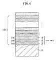
- FIG. 6is a cross-sectional view schematically showing a structure of a multi-layer film according to a second embodiment of the present invention.
- FIG. 7is a cross-sectional view schematically showing a structure of an npn heterojunction bipolar transistor (HBT) according to a third embodiment of the present invention.
- HBTnpn heterojunction bipolar transistor
- FIG. 8is a cross-sectional view showing a structure of the emitter-base-collector junction shown in FIG. 7 under magnification.
- FIG. 9is an energy band diagram schematically illustrating a band structure in cross-section through an emitter layer, a base layer and a collector layer when no bias is applied.
- FIG. 10is a cross-sectional view showing a structure of a heterojunction CMIS device (HCMIS device) utilizing a multi-layer film serving as a SiGeC layer for a p-channel, according to a fourth embodiment of the present invention.
- HCMIS deviceheterojunction CMIS device
- FIG. 11is a diagram conceptually showing a band state in a structure where a silicon layer, the multi-layer film and a silicon layer are stacked in the HCMIS device of the fourth embodiment.
- FIG. 2is a cross-sectional view schematically showing a structure of a multi-layer film (a semiconductor crystal film) according to a first embodiment of the present invention.
- a Si 0.2 Ge 0.8 layer 12 with a thickness of about 1 nm having a larger lattice constant than Si crystal and a Si 0.785 Ge 0.2 C 0.015 layer 13 with a thickness of about 1 nmare alternately deposited on a Si substrate 11 a plurality of times (50 cycles in this embodiment), thereby forming a multi-layer film 10 A serving as a SiGeC layer with a thickness of about 100 nm.
- the multi-layer film 10 A of this embodimentis considered to have a superlattice structure with little discrete quantum levels.
- FIGS. 3 ( a ) through 3 ( e )are cross-sectional views showing respective process steps for producing a semiconductor crystal film according to the first embodiment.
- the Si 0.2 Ge 0.8 layer 12 and the Si 0.785 Ge 0.2 C 0.015 layer 13are deposited by an UHV-CVD process.
- pretreatment of the substrateis very important in general. Thus, the pretreatment of the Si substrate 11 will be initially described.
- a pre-cleaned Si substrate 11is prepared.
- the Si substrate 11is cleaned with a mixed solution of sulfuric acid—hydrogen peroxide aqueous solution, to remove organic materials and metal contaminations on the surface of the Si substrate 11 .
- the Si substrate 11is cleaned with an ammonia—hydrogen peroxide aqueous solution, to remove attachments on the surface of the Si substrate 11 .
- a natural oxide film on the surface of the Si substrate 11is removed by cleaning with hydrofluoric acid solution. At this time, foreign matter as well as an oxide film of the natural oxide film is removed from the surface of the Si substrate 11 .
- the Si substrate 11is immersed in the solution of ammonia—hydrogen peroxide aqueous solution, to form a thin protection oxide film 21 on the surface of the Si substrate 11 .
- the protection oxide film 21which has a relatively uniform thickness and covers the Si substrate 11 , has a function of preventing foreign matter except for the oxide film from attaching to Si atoms in the Si substrate 11 . Accordingly, the protection oxide film 21 allows exposure of the cleaned surface of the Si substrate 11 to go smoothly before the epitaxial growth starts.
- the pretreated Si substrate 11is introduced into a chamber (not shown) in crystal growth apparatus.
- the chamberis one evacuated to about 2 ⁇ 10 ⁇ 9 Torr ( ⁇ 2.7 ⁇ 10 ⁇ 7 Pa) and the Si substrate 11 is heated to a temperature of 850° C. in a hydrogen gas atmosphere.
- the protection oxide film formed on the surface of the Si substrate 11is removed, to expose the cleaned surface of the Si substrate 11 .
- the temperature of the Si substrate 11is decreased to about 490° C. and source gases are introduced into the chamber, to permit crystal growth.
- the Si 0.2 Ge 0.8 layer 12whose composition permits enough growth by a known process, is epitaxially grown on the Si substrate 11 .
- flow rates of the gasesare adjusted such that the partial pressures of Si 2 H 6 and GeH 4 gases are about 7 ⁇ 1 ⁇ 5 Torr ( ⁇ 9.3 ⁇ 10 ⁇ 3 Pa) and 2.8 ⁇ 10 ⁇ 3 Torr ( ⁇ 0.37 Pa), respectively, in the chamber.
- This processis performed for about 5 sec., thereby forming the Si 0.2 Ge 0.8 layer 12 with a thickness of 1 nm.
- the Si 0.785 Ge 0.2 C 0.015 layer 13is then epitaxially grown on the Si 0.2 Ge 0.8 layer 12 .
- flow rates of the source gasesare adjusted such that the partial pressures of Si 2 H 6 , GeH 4 and SiH 3 CH 3 gases are about 7 ⁇ 10 ⁇ 5 Torr ( ⁇ 9.3 ⁇ 10 ⁇ 3 Pa), about 1.7 ⁇ 10 ⁇ 4 Torr ( ⁇ 2.7 Pa) and about 1.3 ⁇ 10 ⁇ 5 Torr ( ⁇ 1.7 ⁇ 10 ⁇ 2 Pa), respectively, in the chamber.
- This processis performed for about 17 sec., thereby forming the Si 0.785 Ge 0.2 C 0.015 layer 13 with a thickness of 1 nm.
- the epitaxial growths of the Si 0.2 Ge 0.8 and Si 0.785 Ge 0.2 C 0.015 layers 12 and 13are alternately repeated under the same conditions as those shown in FIGS. 3 ( c ) and 3 ( d ), thereby forming a multi-layer film 10 A with a superlattice structure in which the Si 0.2 Ge 0.8 /Si 0.785 Ge 0.2 C 0.015 stacked structure constitutes a unit.
- the multi-layer film 10 Ahas, for example, 50 units of the Si 0.2 Ge 0.8 /Si 0.785 Ge 0.2 C 0.015 stacked structures.
- Such stacked structuresresult in the following advantage.
- “Semiconductor and Semimetals Vol. 24”ACADEMIC PRESS, INC. p. 29 Volume Editor RAYMOND DINGLE
- a past literature concerning superlattice structuresif each thickness of layers constituting a superlattice structure is 1.5 nm or less, a discrete quantum levels disappear in the superlattice structure so that the layers act as one crystal.
- the resultant multi-layer film 10 Aserves as a Si 0.4925 Ge 0.5 C 0.0075 layer.
- the multi-layer film 10 Ahas a composition of Si 0.4925 Ge 0.5 C 0.0075 that is an average taken from respective mole fractions of Si, Ge and C in the Si 0.2 Ge 0.8 and Si 0.785 Ge 0.2 C 0.015 layers 12 and 13 .
- the multi-layer film 10 A of this embodimenthas a Ge mole fraction of 50 atm. %, i.e., more than 35 atm. % that is the limit shown in FIG. 1 .
- Cis hardly incorporated into lattice sites in the SiGeC crystal containing about 50 atm. % of Ge.
- the thickness ratio of the Si 0.2 Ge 0.8 layer 12 to the Si 0.785 Ge 0.2 C 0.015 layer 13is not limited to 1:1 but may be an arbitrary ratio.
- FIG. 4is a cross-sectional view schematically showing a structure of a multi-layer film according to a modified example of the first embodiment.
- the Si 0.2 Ge 0.8 layer 12 with a thickness of about 1 nm and the Si 0.785 Ge 0.2 C 0.015 layer 13 with a thickness of about 1.5 nmare alternately deposited on the Si substrate 11 a plurality of times (40 cycles in this modified example), thereby forming a multi-layer film 10 B (a semiconductor crystal film) serving as a SiGeC layer with a thickness of about 100 nm.
- Process steps for forming the multi-layer film 10 B of this modified exampleare basically the same as in the first embodiment, and thus the description thereof will be omitted herein.
- FIG. 5is a diagram showing a composition range in which a single crystal can be produced with a known single-layer SiGeC layer and a composition range for a multi-layer film serving as a SiGeC layer that can be produced according to the present invention.
- the alternate deposition of the Si 0.2 Ge 0.8 and Si 0.785 Ge 0.2 C 0.015 layers 12 and 13results in a multi-layer film serving as a SiGeC layer whose compositional percentages are indicated by any one point corresponding to the ratio of the thickness of the Si 0.2 Ge 0.8 layer 12 to that of the Si 0.785 Ge 0.2 C 0.015 layer 13 on the line L 1 .
- the resultant multi-layer film 10 B(of the modified example of the first embodiment) serves as a SiGeC layer with a composition on the point P 15 shown in FIG. 5 .
- the resultant multi-layer filmserves as a SiGeC layer with a composition indicated by a point on the line L 2 shown in FIG.
- the range in which the multi-layer film serves as a SiGeC layer with C atoms incorporated into lattice sitesextends to the region R 2 shown in FIG. 5 .
- the upper limit of the C mole fraction with C atoms incorporated into lattice sites in a single-layer SiGeC or SiC layeris more than the upper limit shown in FIG. 1 as described above and is about 2.5 atm. %.
- the Si 0.965 Ge 0.01 C 0.025 layer with a thickness of 1.5 nm or lessC atoms can be incorporated into lattice sites even if the C mole fraction is higher than 2.5 atm. %. Therefore, the present invention makes it possible to produce a multi-layer film serving as a SiGeC layer with a C mole fraction exceeding 2.5 atm. %, as indicated by the broken line L 3 shown in FIG. 5 .
- any of the layersmay be the lowermost layer, and any of the layers may be the uppermost layer.
- SiCSi 1-y C y
- SiGeCSi 1-y C y
- SiGeCSi 1-y C y
- the following advantagesare obtained. That is to say, in the multi-layer film made up of the SiC and SiGe layers, crystal layers whose lattice constants are greatly different from each other are alternately stacked, so that defects are easily created. Specifically, the SiC layer has a smaller lattice constant than Si, so that tensile strain is created in the SiC layer that is epitaxially grown on Si.
- the SiGe layerhas a larger lattice constant than Si, so that compressive strain is created in the SiGe layer that is epitaxially grown on the Si substrate. Moreover, a greater compressive strain is created in the SiGe layer epitaxially grown on the SiC layer than that created in the Si substrate. Accordingly, if two types of crystals subjected to strains in mutually different directions, i.e., tensile and compressive strains, are alternately deposited, there arises a state in which defects occurs easily.
- a SiGeC layeris used for at least one type of the layers as in the present invention, compressive or tensile strain can be relaxed, thus obtaining a multi-layer film (a semiconductor crystal film) having little defects.
- SiC layersare grown slowly, while SiGeC layers can be grown faster than the SiC layers.
- SiGeC layersare grown slowly, while SiGeC layers can be grown faster than the SiC layers.
- a combination of SiGeC and SiGe layers or a combination of SiGeC layersis preferable for stacking two types of semiconductor layers.
- the inventive multi-layer filmwhich is obtained by alternate epitaxial growths of two crystal films having two mutually different compositions, and the method for producing the film have been described.
- another inventive multi-layer filmthat is obtained by alternate epitaxial growths of three crystal layers having mutually different compositions will be described.
- FIG. 6is a cross-sectional view schematically showing a structure of a multi-layer film (a semiconductor crystal film) according to a second embodiment of the present invention.
- a Si 0.2 Ge 0.8 layer 12 with a thickness of about 1 nm having a larger lattice constant than Si crystal and a Si 0.785 Ge 0.2 C 0.015 layer 13 with a thickness of about 1 nm, and a Si 0.832 Ge 0.15 C 0.018 layer 14 with a thickness of about 1 nmare alternately deposited on a Si substrate 11 a plurality of times (33 cycles in this embodiment), thereby forming a multi-layer film 10 C (a semiconductor crystal film) serving as a SiGeC layer with a thickness of about 99 nm.
- the multi-layer film 10 C of this embodimentis also considered to have a superlattice structure with little discrete quantum levels.
- Process steps for producing the multi-layer film of this embodimentare basically the same as in the first embodiment, and thus the description thereof will be omitted herein.
- pretreatment of the Si substrate 11is performed through the same process steps as in the first embodiment. Then, the temperature of the Si substrate 11 is decreased to about 490° C. and source gases are introduced into the chamber, to permit crystal growth.
- a Si 0.2 Ge 0.8 layer 12 with a thickness of about 1 nm and a Si 0.785 Ge 0.2 C 0.015 layer 13 with a thickness of about 1 nmare epitaxially grown as in the first embodiment.
- a Si 0.832 Ge 0.15 C 0.018 layer 14whose composition permits enough growth by a known process, is epitaxially grown on Si 0.785 Ge 0.2 C 0.015 layer 13 .
- flow rates of the source gasesare adjusted such that the partial pressures of Si 2 H 6 , GeH 4 , and SiH 3 CH 3 gases are about 7 ⁇ 10 ⁇ 5 Torr ( ⁇ 9.3 ⁇ 10 ⁇ 3 Pa), 8.3 ⁇ 10 ⁇ 5 Torr ( ⁇ 1.1 ⁇ 10 ⁇ 4 Pa), and abut 1.8 ⁇ 10 ⁇ 5 Torr ( ⁇ 2.4 ⁇ 10 ⁇ 2 Pa), respectively, in the chamber.
- This processis performed for about 35 sec., thereby forming the Si 0.832 Ge 0.15 C 0.018 layer 14 with a thickness of 1 nm.
- the multi-layer film 10 Chas, for example, 33 units of the Si 0.2 Ge 0.8 /Si 0.785 Ge 0.2 C 0.0015 /Si 0.832 Ge 0.15 C 0.018 stacked structures.
- the multi-layer film 10 C serving as a Si 0.606 Ge 0.383 C 0.011 layer with a thickness of 99 nmis obtained. That is to say, as shown in FIG. 5 , only 0.6 atm. % of C atoms are incorporated into lattice sites with a Ge mole fraction of about 38 atm. % in a single-layer SiGeC layer. On the other hand, since three types of crystal layers are combined in this embodiment, the resultant multi-layer film 10 C (semiconductor crystal film) serves as a SiGeC layer containing about 1.1 atm. % of C atoms incorporated into lattice sites.
- the inventive multi-layer filmis not limited to these embodiments. That is to say, the inventive multi-layer film is also obtained by alternately stacking more than three types of crystal layers.
- two of the three or more types of crystal layersneed to be a Si 1-x1-y1 Ge x1 C y1 layer (where 0 ⁇ x1 ⁇ 1 and 0 ⁇ y1 ⁇ 1), a Si 1-x2-y2 Ge x2 C y2 layer (where 0 ⁇ x2 ⁇ 1 and 0 ⁇ y2 ⁇ 1, x1 ⁇ x2 and y1>y2), and a Si 1-x1-y1 Ge x1 C y1 layer (where 0 ⁇ x1 ⁇ 1 and 0 ⁇ y1 ⁇ 1).
- the deposition order of the crystal layersis not limited and the same advantageous effects are attained irrespective of the deposition order.
- a Si buffer layermay be epitaxially grown between the multi-layer film 10 A, 10 B or 10 C and the Si substrate 11 , and a Si cap layer may be deposited over the multi-layer film 10 A, 10 B or 10 C, in any of the embodiments.
- FIG. 7is a cross-sectional view schematically showing a structure of an npn heterojunction bipolar transistor (HBT) according to this embodiment.
- the HBT of this embodimentincludes an n 30 layer 31 , which is defined in a Si substrate 30 and contains an n-type dopant (e.g., phosphorus) at a high-concentration; a collector layer 33 , which is epitaxially grown on the n layer 31 and contains an n-type dopant (e.g., phosphorus) at a low-concentration; and isolation layer 32 of a thermal oxide film, which defines the collector layer 33 ; a first deposited oxide film 35 formed on the isolation layer 32 ; a multi-layer film 36 , which fills in an opening (an opening for base) formed in the isolation layer 32 and the first deposited oxide film 35 to extend over the first deposited oxide film 35 and which serves as an SiGeC layer; a second deposited oxide film 37 farmed on the multi-player film 36
- FIG. 8is a cross-sectional view showing a structure of the emitter-base-collector junction shown in FIG. 7 under magnification.
- the multi-layer film 36which has been formed on the collector layer 33 of a Si layer and serves as a SiGeC layer, is formed by alternately stacking the Si 0.2 Ge 0.8 layer 36 a with a thickness of about 1 nm and a Si 0.785 Ge 0.2 C 0.015 layer 36 b with a thickness of about 1 nm a plurality of times (25 cycles in this embodiment), thus obtaining a total thickness of about 50 nm. That is to say, the resultant multi-layer film 36 serves as a Si 0.4925 Ge 0.5 C 0.0075 layer.
- the multi-layer film 36contains boron (B), which is a p-type dopant, and serves as a base layer.
- the emitter layer 38 formed on the multi-layer film 36contains arsenic (As), which is an n-type dopant.
- diboraneB 2 H 6
- Si 0.2 Ge 0.8 and Si 0.785 Ge 0.2 C 0.015 layers 36 a and 36 bare added in each of the epitaxial growths of the Si 0.2 Ge 0.8 and Si 0.785 Ge 0.2 C 0.015 layers 36 a and 36 b performed by the process steps described in the first embodiment.
- Other process stepscan be performed by known techniques, and thus the description thereof will be omitted.
- the multi-layer film 36functioning as base, serves as a Si 0.4925 Ge 0.5 C 0.0075 layer having as high as about 50 atm. % of Ge mole fraction.
- high heterobarriersare formed at the valence and conduction band edges in the junction between the base and emitter layers.
- FIG. 9is an energy band diagram schematically illustrating a band structure in cross-section through the emitter layer 38 , the multi-layer film 36 serving as a base layer and the collector layer 33 when no bias is applied.
- the multi-layer film 36serves as a SiGeC layer having a high Ge mole fraction, thus ensuring wide band offset between the multi-layer film 36 and each of the emitter layer 38 and the collector layer, which are made of Si layers and respectively located on and under the multi-layer film 36 .
- the band offset ⁇ Ec at the conduction band edgecan be set small and the band offset ⁇ Ev at the valence band edge can be set high. That is to say, even if a low bias is applied between the emitter and base, it is possible to obtain current caused by a sufficiently large amount of electrons and to reduce current caused by holes inversely flowing, i.e., from the base to the emitter, thus achieving a HBT which has a high current gain and operates at low voltages.
- a simulation performed by the present inventorsshows that HBTs using the inventive multi-layer film as its base can operate at a low voltage of about 0.45 V.
- the multi-layer film 36 serving as a base layercontains about 0.75 atm. % of C, so that strain created in the multi-layer film 36 serving as a base layer is reduced as a whole. As a result, crystal defects are less created during heat treatment in the process.
- Ge mole fractionis about 50 atm. %, C is hardly incorporated into crystal sites. As a result, defects are likely to occur, thus deteriorating device characteristics.
- FIG. 10is a cross-sectional view showing a structure of a heterojunction MISFET (HMISFET) using a multi-layer film serving as a SiGeC layer for a p-channel, according to a fourth embodiment of the present invention.
- HMISFETheterojunction MISFET
- the HMISFET of this embodimentis provided above an n-well 61 formed on a Si substrate 50 .
- a silicon layer 62On the n-well 61 , a silicon layer 62 ; a multi-layer film 63 , formed by stacking, ten times, a Si 0.2 Ge 0.8 layer with a thickness of 1 nm and a Si 0.785 Ge 0.2 C 0.015 layer with a thickness of 1 nm; and a silicon cap layer 64 are stacked in this order by an UHV-CVD process.
- the multi-layer film 63is made of the film used for a multi-layer film 53 and serves as a Si 0.4925 Ge 0.5 C 0.0075 layer as a whole, to be a channel region through which holes flow.
- a gate insulating film made of a silicon oxide film formed by thermally oxidizing the silicon cap layer 64is provided on the silicon cap layer 64 .
- a gate electrode 66is provided on the gate insulating film. Source/drain regions 67 and 68 of a p + layer are defined below either side of the gate electrode 66 . Source/drain electrodes 69 and 70 are formed on the source/drain regions 67 and 68 , respectively.
- FIG. 11is a diagram conceptually showing a band state in a structure where the silicon layer, multi-layer film and silicon layer are stacked in the HMISFET of this embodiment.
- the conductivity type of a dopantis not taken into account.
- the multi-layer film serving as a SiGeC layerhas a high Ge mole fraction in this embodiment, a high heterobarrier for confining carriers therein is formed at the valence band edge by utilizing wide bandgaps between the multi-layer film and each of the two silicon layers sandwiching the multi-layer film therebetween. Accordingly, a p-channel region exhibiting high efficiency in confining holes can be formed.
- the adjustable ranges of Ge and C mole fractionsare extended to high degrees as described above, the ratio of the height of the heterobarrier formed at the conduction band edge to the height of the heterobarrier formed at the valence band edge can be adjusted to a desired value.
- a multi-layer film of a film used for a multi-layer film of a p-MISFETit is possible to fabricate a CMIS device exhibiting high efficiency in confining both electrons and holes.
- each of the semiconductor layers (Si 1-x1-y1 Ge x1 C y1 and Si 1-x2-y2 Ge x2 C y2 layers) in the multi-layer filmis thin (e.g., about 1.5 nm or less) such that discrete quantum levels do not exist in the layer.
- advantages of the present inventioncan be obtained so long as the multi-layer film serves as a SiGeC layer as a whole.
- the boundary of the layersbecomes unclear by performing heat treatment at about 900° C.
- the whole of the multi-layer filmserves as a SiGeC layer with ease.
- a base layer with a graded compositionsuch that a bandgap becomes narrower from the emitter layer to the collector layer.
- multi-layer filmsto the base layer of the HBT and to each channel region of the CMIS devices have been described. Further, the inventive multi-layer films are also applicable to other heterojunction devices such as resonant tunnel diodes (RTD).
- RTDresonant tunnel diodes
- a semiconductor crystal filmwhich is a multi-layer film serving as a SiGeC layer with a high Ge mole fraction and a high C mole fraction, a method for producing the layer, a semiconductor device and a method for fabricating the device.
- the inventive semiconductor crystal film used for channel regions of heterojunction bipolar transistors or CMIS devicescan be incorporated in various kind of electric units such as information and communication units and computers.
Landscapes
- Engineering & Computer Science (AREA)
- Microelectronics & Electronic Packaging (AREA)
- Condensed Matter Physics & Semiconductors (AREA)
- General Physics & Mathematics (AREA)
- Manufacturing & Machinery (AREA)
- Computer Hardware Design (AREA)
- Physics & Mathematics (AREA)
- Power Engineering (AREA)
- Chemical & Material Sciences (AREA)
- Materials Engineering (AREA)
- Bipolar Transistors (AREA)
- Recrystallisation Techniques (AREA)
- Insulated Gate Type Field-Effect Transistor (AREA)
Abstract
Description
Claims (23)
Applications Claiming Priority (3)
| Application Number | Priority Date | Filing Date | Title |
|---|---|---|---|
| JP2001022962 | 2001-01-31 | ||
| JP2001-022962 | 2001-01-31 | ||
| PCT/JP2002/000737WO2002061842A1 (en) | 2001-01-31 | 2002-01-30 | Semiconductor crystal film and method for preparation thereof |
Publications (2)
| Publication Number | Publication Date |
|---|---|
| US20040092085A1 US20040092085A1 (en) | 2004-05-13 |
| US6852602B2true US6852602B2 (en) | 2005-02-08 |
Family
ID=18888300
Family Applications (1)
| Application Number | Title | Priority Date | Filing Date |
|---|---|---|---|
| US10/298,000Expired - Fee RelatedUS6852602B2 (en) | 2001-01-31 | 2002-01-30 | Semiconductor crystal film and method for preparation thereof |
Country Status (3)
| Country | Link |
|---|---|
| US (1) | US6852602B2 (en) |
| TW (1) | TW531891B (en) |
| WO (1) | WO2002061842A1 (en) |
Cited By (49)
| Publication number | Priority date | Publication date | Assignee | Title |
|---|---|---|---|---|
| US20060046507A1 (en)* | 2004-08-31 | 2006-03-02 | Sharp Laboratories Of America, Inc. | Method to stabilize carbon in Si1-x-yGexCy layers |
| US20070238258A1 (en)* | 2006-03-30 | 2007-10-11 | International Business Machines Corporation | Selective links in silicon hetero-junction bipolar transistors using carbon doping and method of forming same |
| US20110121404A1 (en)* | 2009-09-30 | 2011-05-26 | Lucian Shifren | Advanced transistors with punch through suppression |
| US20120061639A1 (en)* | 2010-09-14 | 2012-03-15 | Naoki Yasuda | Resistance change memory |
| US8404551B2 (en) | 2010-12-03 | 2013-03-26 | Suvolta, Inc. | Source/drain extension control for advanced transistors |
| US8461875B1 (en) | 2011-02-18 | 2013-06-11 | Suvolta, Inc. | Digital circuits having improved transistors, and methods therefor |
| US8525271B2 (en) | 2011-03-03 | 2013-09-03 | Suvolta, Inc. | Semiconductor structure with improved channel stack and method for fabrication thereof |
| US8530286B2 (en) | 2010-04-12 | 2013-09-10 | Suvolta, Inc. | Low power semiconductor transistor structure and method of fabrication thereof |
| US8569156B1 (en) | 2011-05-16 | 2013-10-29 | Suvolta, Inc. | Reducing or eliminating pre-amorphization in transistor manufacture |
| US8569128B2 (en) | 2010-06-21 | 2013-10-29 | Suvolta, Inc. | Semiconductor structure and method of fabrication thereof with mixed metal types |
| US8599623B1 (en) | 2011-12-23 | 2013-12-03 | Suvolta, Inc. | Circuits and methods for measuring circuit elements in an integrated circuit device |
| US8614128B1 (en) | 2011-08-23 | 2013-12-24 | Suvolta, Inc. | CMOS structures and processes based on selective thinning |
| US8629016B1 (en) | 2011-07-26 | 2014-01-14 | Suvolta, Inc. | Multiple transistor types formed in a common epitaxial layer by differential out-diffusion from a doped underlayer |
| US8637955B1 (en) | 2012-08-31 | 2014-01-28 | Suvolta, Inc. | Semiconductor structure with reduced junction leakage and method of fabrication thereof |
| US8645878B1 (en) | 2011-08-23 | 2014-02-04 | Suvolta, Inc. | Porting a circuit design from a first semiconductor process to a second semiconductor process |
| US8713511B1 (en) | 2011-09-16 | 2014-04-29 | Suvolta, Inc. | Tools and methods for yield-aware semiconductor manufacturing process target generation |
| US8735987B1 (en) | 2011-06-06 | 2014-05-27 | Suvolta, Inc. | CMOS gate stack structures and processes |
| US8748270B1 (en) | 2011-03-30 | 2014-06-10 | Suvolta, Inc. | Process for manufacturing an improved analog transistor |
| US8748986B1 (en) | 2011-08-05 | 2014-06-10 | Suvolta, Inc. | Electronic device with controlled threshold voltage |
| US8759872B2 (en) | 2010-06-22 | 2014-06-24 | Suvolta, Inc. | Transistor with threshold voltage set notch and method of fabrication thereof |
| US8796048B1 (en) | 2011-05-11 | 2014-08-05 | Suvolta, Inc. | Monitoring and measurement of thin film layers |
| US8811068B1 (en) | 2011-05-13 | 2014-08-19 | Suvolta, Inc. | Integrated circuit devices and methods |
| US8819603B1 (en) | 2011-12-15 | 2014-08-26 | Suvolta, Inc. | Memory circuits and methods of making and designing the same |
| US8816754B1 (en) | 2012-11-02 | 2014-08-26 | Suvolta, Inc. | Body bias circuits and methods |
| US8863064B1 (en) | 2012-03-23 | 2014-10-14 | Suvolta, Inc. | SRAM cell layout structure and devices therefrom |
| US8877619B1 (en) | 2012-01-23 | 2014-11-04 | Suvolta, Inc. | Process for manufacture of integrated circuits with different channel doping transistor architectures and devices therefrom |
| US8883600B1 (en) | 2011-12-22 | 2014-11-11 | Suvolta, Inc. | Transistor having reduced junction leakage and methods of forming thereof |
| US8895327B1 (en) | 2011-12-09 | 2014-11-25 | Suvolta, Inc. | Tipless transistors, short-tip transistors, and methods and circuits therefor |
| US8970289B1 (en) | 2012-01-23 | 2015-03-03 | Suvolta, Inc. | Circuits and devices for generating bi-directional body bias voltages, and methods therefor |
| US8995204B2 (en) | 2011-06-23 | 2015-03-31 | Suvolta, Inc. | Circuit devices and methods having adjustable transistor body bias |
| US8999861B1 (en) | 2011-05-11 | 2015-04-07 | Suvolta, Inc. | Semiconductor structure with substitutional boron and method for fabrication thereof |
| US9041126B2 (en) | 2012-09-21 | 2015-05-26 | Mie Fujitsu Semiconductor Limited | Deeply depleted MOS transistors having a screening layer and methods thereof |
| US9054219B1 (en) | 2011-08-05 | 2015-06-09 | Mie Fujitsu Semiconductor Limited | Semiconductor devices having fin structures and fabrication methods thereof |
| US9070477B1 (en) | 2012-12-12 | 2015-06-30 | Mie Fujitsu Semiconductor Limited | Bit interleaved low voltage static random access memory (SRAM) and related methods |
| US9093550B1 (en) | 2012-01-31 | 2015-07-28 | Mie Fujitsu Semiconductor Limited | Integrated circuits having a plurality of high-K metal gate FETs with various combinations of channel foundation structure and gate stack structure and methods of making same |
| US9093997B1 (en) | 2012-11-15 | 2015-07-28 | Mie Fujitsu Semiconductor Limited | Slew based process and bias monitors and related methods |
| US9112484B1 (en) | 2012-12-20 | 2015-08-18 | Mie Fujitsu Semiconductor Limited | Integrated circuit process and bias monitors and related methods |
| US9112057B1 (en) | 2012-09-18 | 2015-08-18 | Mie Fujitsu Semiconductor Limited | Semiconductor devices with dopant migration suppression and method of fabrication thereof |
| US9236466B1 (en) | 2011-10-07 | 2016-01-12 | Mie Fujitsu Semiconductor Limited | Analog circuits having improved insulated gate transistors, and methods therefor |
| US9268885B1 (en) | 2013-02-28 | 2016-02-23 | Mie Fujitsu Semiconductor Limited | Integrated circuit device methods and models with predicted device metric variations |
| US9299698B2 (en) | 2012-06-27 | 2016-03-29 | Mie Fujitsu Semiconductor Limited | Semiconductor structure with multiple transistors having various threshold voltages |
| US9299801B1 (en) | 2013-03-14 | 2016-03-29 | Mie Fujitsu Semiconductor Limited | Method for fabricating a transistor device with a tuned dopant profile |
| US9319013B2 (en) | 2014-08-19 | 2016-04-19 | Mie Fujitsu Semiconductor Limited | Operational amplifier input offset correction with transistor threshold voltage adjustment |
| US9406567B1 (en) | 2012-02-28 | 2016-08-02 | Mie Fujitsu Semiconductor Limited | Method for fabricating multiple transistor devices on a substrate with varying threshold voltages |
| US9431068B2 (en) | 2012-10-31 | 2016-08-30 | Mie Fujitsu Semiconductor Limited | Dynamic random access memory (DRAM) with low variation transistor peripheral circuits |
| US9478571B1 (en) | 2013-05-24 | 2016-10-25 | Mie Fujitsu Semiconductor Limited | Buried channel deeply depleted channel transistor |
| US9710006B2 (en) | 2014-07-25 | 2017-07-18 | Mie Fujitsu Semiconductor Limited | Power up body bias circuits and methods |
| US10074568B2 (en) | 2009-09-30 | 2018-09-11 | Mie Fujitsu Semiconductor Limited | Electronic devices and systems, and methods for making and using same |
| US11489041B2 (en)* | 2019-07-01 | 2022-11-01 | Research & Business Foundation Sungkyunkwan University | Semiconductor device and manufacturing method thereof |
Families Citing this family (6)
| Publication number | Priority date | Publication date | Assignee | Title |
|---|---|---|---|---|
| US6744079B2 (en)* | 2002-03-08 | 2004-06-01 | International Business Machines Corporation | Optimized blocking impurity placement for SiGe HBTs |
| US7517768B2 (en)* | 2003-03-31 | 2009-04-14 | Intel Corporation | Method for fabricating a heterojunction bipolar transistor |
| US7195963B2 (en)* | 2004-05-21 | 2007-03-27 | Freescale Semiconductor, Inc. | Method for making a semiconductor structure using silicon germanium |
| US7384829B2 (en)* | 2004-07-23 | 2008-06-10 | International Business Machines Corporation | Patterned strained semiconductor substrate and device |
| US7102205B2 (en)* | 2004-09-01 | 2006-09-05 | International Business Machines Corporation | Bipolar transistor with extrinsic stress layer |
| TWI626746B (en)* | 2014-04-03 | 2018-06-11 | 財團法人工業技術研究院 | Semiconductor structure |
Citations (19)
| Publication number | Priority date | Publication date | Assignee | Title |
|---|---|---|---|---|
| EP0020898A1 (en) | 1979-06-18 | 1981-01-07 | International Business Machines Corporation | An apparatus for controlling the electrical parameters of an electrode reaction in an electrochemical cell |
| JPH05102177A (en) | 1991-10-02 | 1993-04-23 | Hitachi Ltd | Semiconductor integrated circuit device and electronic computer using same |
| JPH06224127A (en) | 1993-01-27 | 1994-08-12 | Nec Corp | Method and device for growth of silicon film |
| JPH0722330A (en) | 1993-06-29 | 1995-01-24 | Oki Electric Ind Co Ltd | Method for forming strain hetero epitaxial layer |
| US5523592A (en)* | 1993-02-03 | 1996-06-04 | Hitachi, Ltd. | Semiconductor optical device, manufacturing method for the same, and opto-electronic integrated circuit using the same |
| JPH09283533A (en) | 1996-04-15 | 1997-10-31 | Matsushita Electric Ind Co Ltd | Heterojunction bipolar transistor |
| JPH11312686A (en) | 1998-04-28 | 1999-11-09 | Matsushita Electric Ind Co Ltd | Semiconductor device and manufacturing method thereof |
| KR20000027652A (en) | 1998-10-28 | 2000-05-15 | 김영환 | Photoelectric devices and method for manufacturing photoelectric devices |
| US6403976B1 (en)* | 1999-01-14 | 2002-06-11 | Matsushita Electric Industrial Co., Ltd. | Semiconductor crystal, fabrication method thereof, and semiconductor device |
| US6403975B1 (en)* | 1996-04-09 | 2002-06-11 | Max-Planck Gesellschaft Zur Forderung Der Wissenschafteneev | Semiconductor components, in particular photodetectors, light emitting diodes, optical modulators and waveguides with multilayer structures grown on silicon substrates |
| US6459107B2 (en)* | 2000-04-28 | 2002-10-01 | Fujitsu Limited | Photodetector having a mixed crystal layer of SiGeC |
| US6475857B1 (en)* | 2001-06-21 | 2002-11-05 | Samsung Electronics Co., Ltd. | Method of making a scalable two transistor memory device |
| US20030006415A1 (en)* | 2000-06-27 | 2003-01-09 | Toshiya Yokogawa | Semiconductor device |
| US6509586B2 (en)* | 2000-03-31 | 2003-01-21 | Fujitsu Limited | Semiconductor device, method for fabricating the semiconductor device and semiconductor integrated circuit |
| US6537369B1 (en)* | 2000-03-27 | 2003-03-25 | Matsushita Electric Industrial Co., Ltd. | SiGeC semiconductor crystal and production method thereof |
| US6617653B1 (en)* | 2000-05-31 | 2003-09-09 | Matsushita Electric Industrial Co., Ltd. | Misfet |
| US6667489B2 (en)* | 2001-11-29 | 2003-12-23 | Hitachi, Ltd. | Heterojunction bipolar transistor and method for production thereof |
| US6678296B1 (en)* | 1999-11-05 | 2004-01-13 | Fujitsu Limited | Optical semiconductor device using a SiGeC random mixed crystal |
| US6690035B1 (en)* | 2000-03-03 | 2004-02-10 | Matsushita Electric Industrial Co., Ltd. | Semiconductor device having an active region of alternating layers |
- 2002
- 2002-01-30WOPCT/JP2002/000737patent/WO2002061842A1/ennot_activeCeased
- 2002-01-30USUS10/298,000patent/US6852602B2/ennot_activeExpired - Fee Related
- 2002-01-31TWTW091101668Apatent/TW531891B/ennot_activeIP Right Cessation
Patent Citations (20)
| Publication number | Priority date | Publication date | Assignee | Title |
|---|---|---|---|---|
| EP0020898A1 (en) | 1979-06-18 | 1981-01-07 | International Business Machines Corporation | An apparatus for controlling the electrical parameters of an electrode reaction in an electrochemical cell |
| JPH05102177A (en) | 1991-10-02 | 1993-04-23 | Hitachi Ltd | Semiconductor integrated circuit device and electronic computer using same |
| JPH06224127A (en) | 1993-01-27 | 1994-08-12 | Nec Corp | Method and device for growth of silicon film |
| US5523592A (en)* | 1993-02-03 | 1996-06-04 | Hitachi, Ltd. | Semiconductor optical device, manufacturing method for the same, and opto-electronic integrated circuit using the same |
| JPH0722330A (en) | 1993-06-29 | 1995-01-24 | Oki Electric Ind Co Ltd | Method for forming strain hetero epitaxial layer |
| US6403975B1 (en)* | 1996-04-09 | 2002-06-11 | Max-Planck Gesellschaft Zur Forderung Der Wissenschafteneev | Semiconductor components, in particular photodetectors, light emitting diodes, optical modulators and waveguides with multilayer structures grown on silicon substrates |
| JPH09283533A (en) | 1996-04-15 | 1997-10-31 | Matsushita Electric Ind Co Ltd | Heterojunction bipolar transistor |
| JPH11312686A (en) | 1998-04-28 | 1999-11-09 | Matsushita Electric Ind Co Ltd | Semiconductor device and manufacturing method thereof |
| KR20000027652A (en) | 1998-10-28 | 2000-05-15 | 김영환 | Photoelectric devices and method for manufacturing photoelectric devices |
| US6403976B1 (en)* | 1999-01-14 | 2002-06-11 | Matsushita Electric Industrial Co., Ltd. | Semiconductor crystal, fabrication method thereof, and semiconductor device |
| US6678296B1 (en)* | 1999-11-05 | 2004-01-13 | Fujitsu Limited | Optical semiconductor device using a SiGeC random mixed crystal |
| US6690035B1 (en)* | 2000-03-03 | 2004-02-10 | Matsushita Electric Industrial Co., Ltd. | Semiconductor device having an active region of alternating layers |
| US6660393B2 (en)* | 2000-03-27 | 2003-12-09 | Matsushita Electric Industrial Co., Ltd. | SiGeC semiconductor crystals and the method producing the same |
| US6537369B1 (en)* | 2000-03-27 | 2003-03-25 | Matsushita Electric Industrial Co., Ltd. | SiGeC semiconductor crystal and production method thereof |
| US6509586B2 (en)* | 2000-03-31 | 2003-01-21 | Fujitsu Limited | Semiconductor device, method for fabricating the semiconductor device and semiconductor integrated circuit |
| US6459107B2 (en)* | 2000-04-28 | 2002-10-01 | Fujitsu Limited | Photodetector having a mixed crystal layer of SiGeC |
| US6617653B1 (en)* | 2000-05-31 | 2003-09-09 | Matsushita Electric Industrial Co., Ltd. | Misfet |
| US20030006415A1 (en)* | 2000-06-27 | 2003-01-09 | Toshiya Yokogawa | Semiconductor device |
| US6475857B1 (en)* | 2001-06-21 | 2002-11-05 | Samsung Electronics Co., Ltd. | Method of making a scalable two transistor memory device |
| US6667489B2 (en)* | 2001-11-29 | 2003-12-23 | Hitachi, Ltd. | Heterojunction bipolar transistor and method for production thereof |
Non-Patent Citations (5)
| Title |
|---|
| "Dependence of substitutional C incorporation on Ge content for Si1-x-yGexCy crystals grown by ultrahigh vacuum chemical vapor deposition", Y. Kanzawa et al., Applied Physics Letters, vol. 77, No. 24, Dec. 11, 2000, pp. 3962-3964. |
| "Materials characterization of Si1-x-yGexCy/Si superlattice structures" T. Laursen et al., Thin Solid Films, Oct. 1997, vols. 308 to 309, pp. 358 to 362. |
| "SiGeC: Band gaps, band offsets, optical properties, and potential applications", K. Brunner et al., J. Vac. Sci. Technol. B 16(3), May/Jun. 1998, pp. 1701-1706. |
| "Silicon-Germanium-Carbon Alloys Extending Si Based Heterostructure Engineering" A. Powell et al., Jpn. J. Appl. Phys. vol. 33 (1994) pp. 2388-2391, Part 1, No. 4B, Apr. 1994. |
| "The influence of substitutional carbon on the Si/Ge interdiffusion studied by x-ray diffractometry at superlattice structures" P. Zaumseil, Journal of Physics D Applied Physics, May 1999, vol. 32, No. 10A, pp. A75 to A80. |
Cited By (103)
| Publication number | Priority date | Publication date | Assignee | Title |
|---|---|---|---|---|
| US7935617B2 (en)* | 2004-08-31 | 2011-05-03 | Sharp Laboratories Of America, Inc. | Method to stabilize carbon in Si1-x-yGexCy layers |
| US20060046507A1 (en)* | 2004-08-31 | 2006-03-02 | Sharp Laboratories Of America, Inc. | Method to stabilize carbon in Si1-x-yGexCy layers |
| US7875908B2 (en) | 2006-03-30 | 2011-01-25 | International Business Machines Corporation | Selective links in silicon hetero-junction bipolar transistors using carbon doping and method of forming same |
| US7378324B2 (en)* | 2006-03-30 | 2008-05-27 | International Business Machines Corporation | Selective links in silicon hetero-junction bipolar transistors using carbon doping and method of forming same |
| US20070238258A1 (en)* | 2006-03-30 | 2007-10-11 | International Business Machines Corporation | Selective links in silicon hetero-junction bipolar transistors using carbon doping and method of forming same |
| US11887895B2 (en) | 2009-09-30 | 2024-01-30 | United Semiconductor Japan Co., Ltd. | Electronic devices and systems, and methods for making and using the same |
| US20110121404A1 (en)* | 2009-09-30 | 2011-05-26 | Lucian Shifren | Advanced transistors with punch through suppression |
| US9263523B2 (en) | 2009-09-30 | 2016-02-16 | Mie Fujitsu Semiconductor Limited | Advanced transistors with punch through suppression |
| US9508800B2 (en) | 2009-09-30 | 2016-11-29 | Mie Fujitsu Semiconductor Limited | Advanced transistors with punch through suppression |
| US8421162B2 (en) | 2009-09-30 | 2013-04-16 | Suvolta, Inc. | Advanced transistors with punch through suppression |
| US10074568B2 (en) | 2009-09-30 | 2018-09-11 | Mie Fujitsu Semiconductor Limited | Electronic devices and systems, and methods for making and using same |
| US10217668B2 (en) | 2009-09-30 | 2019-02-26 | Mie Fujitsu Semiconductor Limited | Electronic devices and systems, and methods for making and using the same |
| US10224244B2 (en) | 2009-09-30 | 2019-03-05 | Mie Fujitsu Semiconductor Limited | Electronic devices and systems, and methods for making and using the same |
| US10325986B2 (en) | 2009-09-30 | 2019-06-18 | Mie Fujitsu Semiconductor Limited | Advanced transistors with punch through suppression |
| US11062950B2 (en) | 2009-09-30 | 2021-07-13 | United Semiconductor Japan Co., Ltd. | Electronic devices and systems, and methods for making and using the same |
| US8530286B2 (en) | 2010-04-12 | 2013-09-10 | Suvolta, Inc. | Low power semiconductor transistor structure and method of fabrication thereof |
| US9496261B2 (en) | 2010-04-12 | 2016-11-15 | Mie Fujitsu Semiconductor Limited | Low power semiconductor transistor structure and method of fabrication thereof |
| US9865596B2 (en) | 2010-04-12 | 2018-01-09 | Mie Fujitsu Semiconductor Limited | Low power semiconductor transistor structure and method of fabrication thereof |
| US8569128B2 (en) | 2010-06-21 | 2013-10-29 | Suvolta, Inc. | Semiconductor structure and method of fabrication thereof with mixed metal types |
| US9224733B2 (en) | 2010-06-21 | 2015-12-29 | Mie Fujitsu Semiconductor Limited | Semiconductor structure and method of fabrication thereof with mixed metal types |
| US8759872B2 (en) | 2010-06-22 | 2014-06-24 | Suvolta, Inc. | Transistor with threshold voltage set notch and method of fabrication thereof |
| US9418987B2 (en) | 2010-06-22 | 2016-08-16 | Mie Fujitsu Semiconductor Limited | Transistor with threshold voltage set notch and method of fabrication thereof |
| US9922977B2 (en) | 2010-06-22 | 2018-03-20 | Mie Fujitsu Semiconductor Limited | Transistor with threshold voltage set notch and method of fabrication thereof |
| US20120061639A1 (en)* | 2010-09-14 | 2012-03-15 | Naoki Yasuda | Resistance change memory |
| US8461563B2 (en)* | 2010-09-14 | 2013-06-11 | Kabushiki Kaisha Toshiba | Resistance change memory |
| US8686511B2 (en) | 2010-12-03 | 2014-04-01 | Suvolta, Inc. | Source/drain extension control for advanced transistors |
| US8563384B2 (en) | 2010-12-03 | 2013-10-22 | Suvolta, Inc. | Source/drain extension control for advanced transistors |
| US8404551B2 (en) | 2010-12-03 | 2013-03-26 | Suvolta, Inc. | Source/drain extension control for advanced transistors |
| US9006843B2 (en) | 2010-12-03 | 2015-04-14 | Suvolta, Inc. | Source/drain extension control for advanced transistors |
| US9985631B2 (en) | 2011-02-18 | 2018-05-29 | Mie Fujitsu Semiconductor Limited | Digital circuits having improved transistors, and methods therefor |
| US9184750B1 (en) | 2011-02-18 | 2015-11-10 | Mie Fujitsu Semiconductor Limited | Digital circuits having improved transistors, and methods therefor |
| US8461875B1 (en) | 2011-02-18 | 2013-06-11 | Suvolta, Inc. | Digital circuits having improved transistors, and methods therefor |
| US9838012B2 (en) | 2011-02-18 | 2017-12-05 | Mie Fujitsu Semiconductor Limited | Digital circuits having improved transistors, and methods therefor |
| US10250257B2 (en) | 2011-02-18 | 2019-04-02 | Mie Fujitsu Semiconductor Limited | Digital circuits having improved transistors, and methods therefor |
| US9680470B2 (en) | 2011-02-18 | 2017-06-13 | Mie Fujitsu Semiconductor Limited | Digital circuits having improved transistors, and methods therefor |
| US8525271B2 (en) | 2011-03-03 | 2013-09-03 | Suvolta, Inc. | Semiconductor structure with improved channel stack and method for fabrication thereof |
| US9111785B2 (en) | 2011-03-03 | 2015-08-18 | Mie Fujitsu Semiconductor Limited | Semiconductor structure with improved channel stack and method for fabrication thereof |
| US8748270B1 (en) | 2011-03-30 | 2014-06-10 | Suvolta, Inc. | Process for manufacturing an improved analog transistor |
| US9093469B2 (en) | 2011-03-30 | 2015-07-28 | Mie Fujitsu Semiconductor Limited | Analog transistor |
| US8999861B1 (en) | 2011-05-11 | 2015-04-07 | Suvolta, Inc. | Semiconductor structure with substitutional boron and method for fabrication thereof |
| US8796048B1 (en) | 2011-05-11 | 2014-08-05 | Suvolta, Inc. | Monitoring and measurement of thin film layers |
| US9741428B2 (en) | 2011-05-13 | 2017-08-22 | Mie Fujitsu Semiconductor Limited | Integrated circuit devices and methods |
| US9362291B1 (en) | 2011-05-13 | 2016-06-07 | Mie Fujitsu Semiconductor Limited | Integrated circuit devices and methods |
| US8811068B1 (en) | 2011-05-13 | 2014-08-19 | Suvolta, Inc. | Integrated circuit devices and methods |
| US9966130B2 (en) | 2011-05-13 | 2018-05-08 | Mie Fujitsu Semiconductor Limited | Integrated circuit devices and methods |
| US8937005B2 (en) | 2011-05-16 | 2015-01-20 | Suvolta, Inc. | Reducing or eliminating pre-amorphization in transistor manufacture |
| US9514940B2 (en) | 2011-05-16 | 2016-12-06 | Mie Fujitsu Semiconductor Limited | Reducing or eliminating pre-amorphization in transistor manufacture |
| US9793172B2 (en) | 2011-05-16 | 2017-10-17 | Mie Fujitsu Semiconductor Limited | Reducing or eliminating pre-amorphization in transistor manufacture |
| US8569156B1 (en) | 2011-05-16 | 2013-10-29 | Suvolta, Inc. | Reducing or eliminating pre-amorphization in transistor manufacture |
| US8735987B1 (en) | 2011-06-06 | 2014-05-27 | Suvolta, Inc. | CMOS gate stack structures and processes |
| US9281248B1 (en) | 2011-06-06 | 2016-03-08 | Mie Fujitsu Semiconductor Limited | CMOS gate stack structures and processes |
| US8995204B2 (en) | 2011-06-23 | 2015-03-31 | Suvolta, Inc. | Circuit devices and methods having adjustable transistor body bias |
| US8629016B1 (en) | 2011-07-26 | 2014-01-14 | Suvolta, Inc. | Multiple transistor types formed in a common epitaxial layer by differential out-diffusion from a doped underlayer |
| US8916937B1 (en) | 2011-07-26 | 2014-12-23 | Suvolta, Inc. | Multiple transistor types formed in a common epitaxial layer by differential out-diffusion from a doped underlayer |
| US8653604B1 (en) | 2011-07-26 | 2014-02-18 | Suvolta, Inc. | Multiple transistor types formed in a common epitaxial layer by differential out-diffusion from a doped underlayer |
| US9054219B1 (en) | 2011-08-05 | 2015-06-09 | Mie Fujitsu Semiconductor Limited | Semiconductor devices having fin structures and fabrication methods thereof |
| US8963249B1 (en) | 2011-08-05 | 2015-02-24 | Suvolta, Inc. | Electronic device with controlled threshold voltage |
| US8748986B1 (en) | 2011-08-05 | 2014-06-10 | Suvolta, Inc. | Electronic device with controlled threshold voltage |
| US8645878B1 (en) | 2011-08-23 | 2014-02-04 | Suvolta, Inc. | Porting a circuit design from a first semiconductor process to a second semiconductor process |
| US8806395B1 (en) | 2011-08-23 | 2014-08-12 | Suvolta, Inc. | Porting a circuit design from a first semiconductor process to a second semiconductor process |
| US9391076B1 (en) | 2011-08-23 | 2016-07-12 | Mie Fujitsu Semiconductor Limited | CMOS structures and processes based on selective thinning |
| US9117746B1 (en) | 2011-08-23 | 2015-08-25 | Mie Fujitsu Semiconductor Limited | Porting a circuit design from a first semiconductor process to a second semiconductor process |
| US8614128B1 (en) | 2011-08-23 | 2013-12-24 | Suvolta, Inc. | CMOS structures and processes based on selective thinning |
| US8713511B1 (en) | 2011-09-16 | 2014-04-29 | Suvolta, Inc. | Tools and methods for yield-aware semiconductor manufacturing process target generation |
| US9236466B1 (en) | 2011-10-07 | 2016-01-12 | Mie Fujitsu Semiconductor Limited | Analog circuits having improved insulated gate transistors, and methods therefor |
| US8895327B1 (en) | 2011-12-09 | 2014-11-25 | Suvolta, Inc. | Tipless transistors, short-tip transistors, and methods and circuits therefor |
| US8819603B1 (en) | 2011-12-15 | 2014-08-26 | Suvolta, Inc. | Memory circuits and methods of making and designing the same |
| US9196727B2 (en) | 2011-12-22 | 2015-11-24 | Mie Fujitsu Semiconductor Limited | High uniformity screen and epitaxial layers for CMOS devices |
| US8883600B1 (en) | 2011-12-22 | 2014-11-11 | Suvolta, Inc. | Transistor having reduced junction leakage and methods of forming thereof |
| US9368624B2 (en) | 2011-12-22 | 2016-06-14 | Mie Fujitsu Semiconductor Limited | Method for fabricating a transistor with reduced junction leakage current |
| US8599623B1 (en) | 2011-12-23 | 2013-12-03 | Suvolta, Inc. | Circuits and methods for measuring circuit elements in an integrated circuit device |
| US8970289B1 (en) | 2012-01-23 | 2015-03-03 | Suvolta, Inc. | Circuits and devices for generating bi-directional body bias voltages, and methods therefor |
| US8877619B1 (en) | 2012-01-23 | 2014-11-04 | Suvolta, Inc. | Process for manufacture of integrated circuits with different channel doping transistor architectures and devices therefrom |
| US9385047B2 (en) | 2012-01-31 | 2016-07-05 | Mie Fujitsu Semiconductor Limited | Integrated circuits having a plurality of high-K metal gate FETs with various combinations of channel foundation structure and gate stack structure and methods of making same |
| US9093550B1 (en) | 2012-01-31 | 2015-07-28 | Mie Fujitsu Semiconductor Limited | Integrated circuits having a plurality of high-K metal gate FETs with various combinations of channel foundation structure and gate stack structure and methods of making same |
| US9406567B1 (en) | 2012-02-28 | 2016-08-02 | Mie Fujitsu Semiconductor Limited | Method for fabricating multiple transistor devices on a substrate with varying threshold voltages |
| US8863064B1 (en) | 2012-03-23 | 2014-10-14 | Suvolta, Inc. | SRAM cell layout structure and devices therefrom |
| US10014387B2 (en) | 2012-06-27 | 2018-07-03 | Mie Fujitsu Semiconductor Limited | Semiconductor structure with multiple transistors having various threshold voltages |
| US9812550B2 (en) | 2012-06-27 | 2017-11-07 | Mie Fujitsu Semiconductor Limited | Semiconductor structure with multiple transistors having various threshold voltages |
| US10217838B2 (en) | 2012-06-27 | 2019-02-26 | Mie Fujitsu Semiconductor Limited | Semiconductor structure with multiple transistors having various threshold voltages |
| US9299698B2 (en) | 2012-06-27 | 2016-03-29 | Mie Fujitsu Semiconductor Limited | Semiconductor structure with multiple transistors having various threshold voltages |
| US8637955B1 (en) | 2012-08-31 | 2014-01-28 | Suvolta, Inc. | Semiconductor structure with reduced junction leakage and method of fabrication thereof |
| US9105711B2 (en) | 2012-08-31 | 2015-08-11 | Mie Fujitsu Semiconductor Limited | Semiconductor structure with reduced junction leakage and method of fabrication thereof |
| US9112057B1 (en) | 2012-09-18 | 2015-08-18 | Mie Fujitsu Semiconductor Limited | Semiconductor devices with dopant migration suppression and method of fabrication thereof |
| US9041126B2 (en) | 2012-09-21 | 2015-05-26 | Mie Fujitsu Semiconductor Limited | Deeply depleted MOS transistors having a screening layer and methods thereof |
| US9431068B2 (en) | 2012-10-31 | 2016-08-30 | Mie Fujitsu Semiconductor Limited | Dynamic random access memory (DRAM) with low variation transistor peripheral circuits |
| US9154123B1 (en) | 2012-11-02 | 2015-10-06 | Mie Fujitsu Semiconductor Limited | Body bias circuits and methods |
| US8816754B1 (en) | 2012-11-02 | 2014-08-26 | Suvolta, Inc. | Body bias circuits and methods |
| US9093997B1 (en) | 2012-11-15 | 2015-07-28 | Mie Fujitsu Semiconductor Limited | Slew based process and bias monitors and related methods |
| US9319034B2 (en) | 2012-11-15 | 2016-04-19 | Mie Fujitsu Semiconductor Limited | Slew based process and bias monitors and related methods |
| US9070477B1 (en) | 2012-12-12 | 2015-06-30 | Mie Fujitsu Semiconductor Limited | Bit interleaved low voltage static random access memory (SRAM) and related methods |
| US9276561B2 (en) | 2012-12-20 | 2016-03-01 | Mie Fujitsu Semiconductor Limited | Integrated circuit process and bias monitors and related methods |
| US9112484B1 (en) | 2012-12-20 | 2015-08-18 | Mie Fujitsu Semiconductor Limited | Integrated circuit process and bias monitors and related methods |
| US9268885B1 (en) | 2013-02-28 | 2016-02-23 | Mie Fujitsu Semiconductor Limited | Integrated circuit device methods and models with predicted device metric variations |
| US9299801B1 (en) | 2013-03-14 | 2016-03-29 | Mie Fujitsu Semiconductor Limited | Method for fabricating a transistor device with a tuned dopant profile |
| US9577041B2 (en) | 2013-03-14 | 2017-02-21 | Mie Fujitsu Semiconductor Limited | Method for fabricating a transistor device with a tuned dopant profile |
| US9893148B2 (en) | 2013-03-14 | 2018-02-13 | Mie Fujitsu Semiconductor Limited | Method for fabricating a transistor device with a tuned dopant profile |
| US9991300B2 (en) | 2013-05-24 | 2018-06-05 | Mie Fujitsu Semiconductor Limited | Buried channel deeply depleted channel transistor |
| US9478571B1 (en) | 2013-05-24 | 2016-10-25 | Mie Fujitsu Semiconductor Limited | Buried channel deeply depleted channel transistor |
| US9786703B2 (en) | 2013-05-24 | 2017-10-10 | Mie Fujitsu Semiconductor Limited | Buried channel deeply depleted channel transistor |
| US9710006B2 (en) | 2014-07-25 | 2017-07-18 | Mie Fujitsu Semiconductor Limited | Power up body bias circuits and methods |
| US9319013B2 (en) | 2014-08-19 | 2016-04-19 | Mie Fujitsu Semiconductor Limited | Operational amplifier input offset correction with transistor threshold voltage adjustment |
| US11489041B2 (en)* | 2019-07-01 | 2022-11-01 | Research & Business Foundation Sungkyunkwan University | Semiconductor device and manufacturing method thereof |
Also Published As
| Publication number | Publication date |
|---|---|
| TW531891B (en) | 2003-05-11 |
| WO2002061842A1 (en) | 2002-08-08 |
| US20040092085A1 (en) | 2004-05-13 |
Similar Documents
| Publication | Publication Date | Title |
|---|---|---|
| US6852602B2 (en) | Semiconductor crystal film and method for preparation thereof | |
| US8441000B2 (en) | Heterojunction tunneling field effect transistors, and methods for fabricating the same | |
| KR101905299B1 (en) | Methods for making a semiconductor device including atomic layer structures using n₂o as an oxygen source | |
| CN100511720C (en) | Heterojunction field effect transistors using silicon-germanium and silicon-carbon alloys | |
| US6403976B1 (en) | Semiconductor crystal, fabrication method thereof, and semiconductor device | |
| US6537369B1 (en) | SiGeC semiconductor crystal and production method thereof | |
| Miyao et al. | Molecular beam epitaxy of silicon-based heterostructure and its application to novel devices | |
| JP3515944B2 (en) | Hetero bipolar transistor | |
| JP3708881B2 (en) | Semiconductor crystal film, manufacturing method thereof, semiconductor device and manufacturing method thereof | |
| JPH05259077A (en) | Semiconductor device and manufacture thereof | |
| JP2020009799A (en) | Tunnel field effect transistor | |
| JP4506035B2 (en) | Semiconductor substrate, field effect transistor, method of forming SiGe layer, method of forming strained Si layer using the same, and method of manufacturing field effect transistor | |
| JP4770130B2 (en) | Epitaxial wafer for field effect transistor and epitaxial wafer for high electron mobility transistor | |
| CN102414789A (en) | Method for producing semiconductor substrate and semiconductor substrate | |
| JP2005203721A (en) | Semiconductor device | |
| KR100460201B1 (en) | Manufacturing method of a virtual substrate for SiGe/Si hetero-junction field-effect transistor | |
| Chrastina et al. | LEPECVD—A production technique for SiGe MOSFETs and MODFETs | |
| Maekawa et al. | Strain-relieving mechanisms of thin double-and triple-layer buffers | |
| Chen et al. | Advances in Si-based nanotechnology and quantum devices | |
| WANG et al. | HIGH MOBILITY TWO-DIMENSIONAL ELECTRON GAS IN MODULATION-DOPED |
Legal Events
| Date | Code | Title | Description |
|---|---|---|---|
| AS | Assignment | Owner name:MATSUSHITA ELECTRIC INDUSTRIAL CO., LTD., JAPAN Free format text:ASSIGNMENT OF ASSIGNORS INTEREST;ASSIGNORS:KANZAWA, YOSHIHIKO;SAITOH, TOHRU;NOZAWA, KATSUYA;AND OTHERS;REEL/FRAME:014213/0607 Effective date:20020930 | |
| AS | Assignment | Owner name:MATSUSHITA ELECTRIC INDUSTRIAL CO., LTD., JAPAN Free format text:CORRECTIVE ASSIGNMENT TO CORRECT 6TH CONVEYING PARTY'S NAME, PREVIOUSLY RECORDED AT REEL 014213, FRAME 0607;ASSIGNORS:KANZAWA, YOSHIHIKO;SAITOH, TOHRU;NOZAWA, KATSUYA;AND OTHERS;REEL/FRAME:015343/0248 Effective date:20020930 | |
| FEPP | Fee payment procedure | Free format text:PAYOR NUMBER ASSIGNED (ORIGINAL EVENT CODE: ASPN); ENTITY STATUS OF PATENT OWNER: LARGE ENTITY | |
| AS | Assignment | Owner name:MATSUSHITA ELECTRIC INDUSTRIAL CO., LTD., JAPAN Free format text:ASSIGNMENT OF ASSIGNORS INTEREST;ASSIGNORS:KANZAWA, YOSHIHIKO;SAITOH, TOHRU;NOZAWA, KATSUYA;AND OTHERS;REEL/FRAME:015970/0146 Effective date:20020930 | |
| CC | Certificate of correction | ||
| FPAY | Fee payment | Year of fee payment:4 | |
| REMI | Maintenance fee reminder mailed | ||
| LAPS | Lapse for failure to pay maintenance fees | ||
| STCH | Information on status: patent discontinuation | Free format text:PATENT EXPIRED DUE TO NONPAYMENT OF MAINTENANCE FEES UNDER 37 CFR 1.362 | |
| FP | Lapsed due to failure to pay maintenance fee | Effective date:20130208 |