US6850312B2 - Apparatuses and methods for flexible displays - Google Patents
Apparatuses and methods for flexible displaysDownload PDFInfo
- Publication number
- US6850312B2 US6850312B2US10/812,788US81278804AUS6850312B2US 6850312 B2US6850312 B2US 6850312B2US 81278804 AUS81278804 AUS 81278804AUS 6850312 B2US6850312 B2US 6850312B2
- Authority
- US
- United States
- Prior art keywords
- substrate
- display
- flexible
- flexible substrate
- display tape
- Prior art date
- Legal status (The legal status is an assumption and is not a legal conclusion. Google has not performed a legal analysis and makes no representation as to the accuracy of the status listed.)
- Expired - Lifetime
Links
Images


Classifications
- H—ELECTRICITY
- H10—SEMICONDUCTOR DEVICES; ELECTRIC SOLID-STATE DEVICES NOT OTHERWISE PROVIDED FOR
- H10D—INORGANIC ELECTRIC SEMICONDUCTOR DEVICES
- H10D86/00—Integrated devices formed in or on insulating or conducting substrates, e.g. formed in silicon-on-insulator [SOI] substrates or on stainless steel or glass substrates
- H10D86/40—Integrated devices formed in or on insulating or conducting substrates, e.g. formed in silicon-on-insulator [SOI] substrates or on stainless steel or glass substrates characterised by multiple TFTs
- G—PHYSICS
- G02—OPTICS
- G02F—OPTICAL DEVICES OR ARRANGEMENTS FOR THE CONTROL OF LIGHT BY MODIFICATION OF THE OPTICAL PROPERTIES OF THE MEDIA OF THE ELEMENTS INVOLVED THEREIN; NON-LINEAR OPTICS; FREQUENCY-CHANGING OF LIGHT; OPTICAL LOGIC ELEMENTS; OPTICAL ANALOGUE/DIGITAL CONVERTERS
- G02F1/00—Devices or arrangements for the control of the intensity, colour, phase, polarisation or direction of light arriving from an independent light source, e.g. switching, gating or modulating; Non-linear optics
- G02F1/01—Devices or arrangements for the control of the intensity, colour, phase, polarisation or direction of light arriving from an independent light source, e.g. switching, gating or modulating; Non-linear optics for the control of the intensity, phase, polarisation or colour
- G02F1/13—Devices or arrangements for the control of the intensity, colour, phase, polarisation or direction of light arriving from an independent light source, e.g. switching, gating or modulating; Non-linear optics for the control of the intensity, phase, polarisation or colour based on liquid crystals, e.g. single liquid crystal display cells
- G02F1/133—Constructional arrangements; Operation of liquid crystal cells; Circuit arrangements
- G02F1/1333—Constructional arrangements; Manufacturing methods
- G02F1/133305—Flexible substrates, e.g. plastics, organic film
- H—ELECTRICITY
- H01—ELECTRIC ELEMENTS
- H01L—SEMICONDUCTOR DEVICES NOT COVERED BY CLASS H10
- H01L24/00—Arrangements for connecting or disconnecting semiconductor or solid-state bodies; Methods or apparatus related thereto
- H01L24/01—Means for bonding being attached to, or being formed on, the surface to be connected, e.g. chip-to-package, die-attach, "first-level" interconnects; Manufacturing methods related thereto
- H01L24/18—High density interconnect [HDI] connectors; Manufacturing methods related thereto
- H01L24/23—Structure, shape, material or disposition of the high density interconnect connectors after the connecting process
- H01L24/24—Structure, shape, material or disposition of the high density interconnect connectors after the connecting process of an individual high density interconnect connector
- H—ELECTRICITY
- H01—ELECTRIC ELEMENTS
- H01L—SEMICONDUCTOR DEVICES NOT COVERED BY CLASS H10
- H01L24/00—Arrangements for connecting or disconnecting semiconductor or solid-state bodies; Methods or apparatus related thereto
- H01L24/80—Methods for connecting semiconductor or other solid state bodies using means for bonding being attached to, or being formed on, the surface to be connected
- H01L24/82—Methods for connecting semiconductor or other solid state bodies using means for bonding being attached to, or being formed on, the surface to be connected by forming build-up interconnects at chip-level, e.g. for high density interconnects [HDI]
- H—ELECTRICITY
- H01—ELECTRIC ELEMENTS
- H01L—SEMICONDUCTOR DEVICES NOT COVERED BY CLASS H10
- H01L24/00—Arrangements for connecting or disconnecting semiconductor or solid-state bodies; Methods or apparatus related thereto
- H01L24/93—Batch processes
- H01L24/95—Batch processes at chip-level, i.e. with connecting carried out on a plurality of singulated devices, i.e. on diced chips
- H01L24/97—Batch processes at chip-level, i.e. with connecting carried out on a plurality of singulated devices, i.e. on diced chips the devices being connected to a common substrate, e.g. interposer, said common substrate being separable into individual assemblies after connecting
- H—ELECTRICITY
- H01—ELECTRIC ELEMENTS
- H01L—SEMICONDUCTOR DEVICES NOT COVERED BY CLASS H10
- H01L25/00—Assemblies consisting of a plurality of semiconductor or other solid state devices
- H01L25/50—Multistep manufacturing processes of assemblies consisting of devices, the devices being individual devices of subclass H10D or integrated devices of class H10
- H—ELECTRICITY
- H10—SEMICONDUCTOR DEVICES; ELECTRIC SOLID-STATE DEVICES NOT OTHERWISE PROVIDED FOR
- H10D—INORGANIC ELECTRIC SEMICONDUCTOR DEVICES
- H10D86/00—Integrated devices formed in or on insulating or conducting substrates, e.g. formed in silicon-on-insulator [SOI] substrates or on stainless steel or glass substrates
- H10D86/40—Integrated devices formed in or on insulating or conducting substrates, e.g. formed in silicon-on-insulator [SOI] substrates or on stainless steel or glass substrates characterised by multiple TFTs
- H10D86/60—Integrated devices formed in or on insulating or conducting substrates, e.g. formed in silicon-on-insulator [SOI] substrates or on stainless steel or glass substrates characterised by multiple TFTs wherein the TFTs are in active matrices
- G—PHYSICS
- G02—OPTICS
- G02F—OPTICAL DEVICES OR ARRANGEMENTS FOR THE CONTROL OF LIGHT BY MODIFICATION OF THE OPTICAL PROPERTIES OF THE MEDIA OF THE ELEMENTS INVOLVED THEREIN; NON-LINEAR OPTICS; FREQUENCY-CHANGING OF LIGHT; OPTICAL LOGIC ELEMENTS; OPTICAL ANALOGUE/DIGITAL CONVERTERS
- G02F1/00—Devices or arrangements for the control of the intensity, colour, phase, polarisation or direction of light arriving from an independent light source, e.g. switching, gating or modulating; Non-linear optics
- G02F1/01—Devices or arrangements for the control of the intensity, colour, phase, polarisation or direction of light arriving from an independent light source, e.g. switching, gating or modulating; Non-linear optics for the control of the intensity, phase, polarisation or colour
- G02F1/13—Devices or arrangements for the control of the intensity, colour, phase, polarisation or direction of light arriving from an independent light source, e.g. switching, gating or modulating; Non-linear optics for the control of the intensity, phase, polarisation or colour based on liquid crystals, e.g. single liquid crystal display cells
- G02F1/133—Constructional arrangements; Operation of liquid crystal cells; Circuit arrangements
- G02F1/136—Liquid crystal cells structurally associated with a semi-conducting layer or substrate, e.g. cells forming part of an integrated circuit
- G02F1/1362—Active matrix addressed cells
- H—ELECTRICITY
- H01—ELECTRIC ELEMENTS
- H01L—SEMICONDUCTOR DEVICES NOT COVERED BY CLASS H10
- H01L2224/00—Indexing scheme for arrangements for connecting or disconnecting semiconductor or solid-state bodies and methods related thereto as covered by H01L24/00
- H01L2224/01—Means for bonding being attached to, or being formed on, the surface to be connected, e.g. chip-to-package, die-attach, "first-level" interconnects; Manufacturing methods related thereto
- H01L2224/18—High density interconnect [HDI] connectors; Manufacturing methods related thereto
- H01L2224/23—Structure, shape, material or disposition of the high density interconnect connectors after the connecting process
- H01L2224/24—Structure, shape, material or disposition of the high density interconnect connectors after the connecting process of an individual high density interconnect connector
- H01L2224/241—Disposition
- H01L2224/24101—Connecting bonding areas at the same height
- H—ELECTRICITY
- H01—ELECTRIC ELEMENTS
- H01L—SEMICONDUCTOR DEVICES NOT COVERED BY CLASS H10
- H01L2224/00—Indexing scheme for arrangements for connecting or disconnecting semiconductor or solid-state bodies and methods related thereto as covered by H01L24/00
- H01L2224/01—Means for bonding being attached to, or being formed on, the surface to be connected, e.g. chip-to-package, die-attach, "first-level" interconnects; Manufacturing methods related thereto
- H01L2224/18—High density interconnect [HDI] connectors; Manufacturing methods related thereto
- H01L2224/23—Structure, shape, material or disposition of the high density interconnect connectors after the connecting process
- H01L2224/24—Structure, shape, material or disposition of the high density interconnect connectors after the connecting process of an individual high density interconnect connector
- H01L2224/241—Disposition
- H01L2224/24135—Connecting between different semiconductor or solid-state bodies, i.e. chip-to-chip
- H01L2224/24137—Connecting between different semiconductor or solid-state bodies, i.e. chip-to-chip the bodies being arranged next to each other, e.g. on a common substrate
- H—ELECTRICITY
- H01—ELECTRIC ELEMENTS
- H01L—SEMICONDUCTOR DEVICES NOT COVERED BY CLASS H10
- H01L2224/00—Indexing scheme for arrangements for connecting or disconnecting semiconductor or solid-state bodies and methods related thereto as covered by H01L24/00
- H01L2224/01—Means for bonding being attached to, or being formed on, the surface to be connected, e.g. chip-to-package, die-attach, "first-level" interconnects; Manufacturing methods related thereto
- H01L2224/18—High density interconnect [HDI] connectors; Manufacturing methods related thereto
- H01L2224/23—Structure, shape, material or disposition of the high density interconnect connectors after the connecting process
- H01L2224/24—Structure, shape, material or disposition of the high density interconnect connectors after the connecting process of an individual high density interconnect connector
- H01L2224/241—Disposition
- H01L2224/24151—Connecting between a semiconductor or solid-state body and an item not being a semiconductor or solid-state body, e.g. chip-to-substrate, chip-to-passive
- H01L2224/24221—Connecting between a semiconductor or solid-state body and an item not being a semiconductor or solid-state body, e.g. chip-to-substrate, chip-to-passive the body and the item being stacked
- H01L2224/24225—Connecting between a semiconductor or solid-state body and an item not being a semiconductor or solid-state body, e.g. chip-to-substrate, chip-to-passive the body and the item being stacked the item being non-metallic, e.g. insulating substrate with or without metallisation
- H01L2224/24227—Connecting between a semiconductor or solid-state body and an item not being a semiconductor or solid-state body, e.g. chip-to-substrate, chip-to-passive the body and the item being stacked the item being non-metallic, e.g. insulating substrate with or without metallisation the HDI interconnect not connecting to the same level of the item at which the semiconductor or solid-state body is mounted, e.g. the semiconductor or solid-state body being mounted in a cavity or on a protrusion of the item
- H—ELECTRICITY
- H01—ELECTRIC ELEMENTS
- H01L—SEMICONDUCTOR DEVICES NOT COVERED BY CLASS H10
- H01L2224/00—Indexing scheme for arrangements for connecting or disconnecting semiconductor or solid-state bodies and methods related thereto as covered by H01L24/00
- H01L2224/74—Apparatus for manufacturing arrangements for connecting or disconnecting semiconductor or solid-state bodies and for methods related thereto
- H01L2224/76—Apparatus for connecting with build-up interconnects
- H01L2224/7615—Means for depositing
- H01L2224/76151—Means for direct writing
- H01L2224/76155—Jetting means, e.g. ink jet
- H—ELECTRICITY
- H01—ELECTRIC ELEMENTS
- H01L—SEMICONDUCTOR DEVICES NOT COVERED BY CLASS H10
- H01L2224/00—Indexing scheme for arrangements for connecting or disconnecting semiconductor or solid-state bodies and methods related thereto as covered by H01L24/00
- H01L2224/74—Apparatus for manufacturing arrangements for connecting or disconnecting semiconductor or solid-state bodies and for methods related thereto
- H01L2224/76—Apparatus for connecting with build-up interconnects
- H01L2224/7665—Means for transporting the components to be connected
- H—ELECTRICITY
- H01—ELECTRIC ELEMENTS
- H01L—SEMICONDUCTOR DEVICES NOT COVERED BY CLASS H10
- H01L2224/00—Indexing scheme for arrangements for connecting or disconnecting semiconductor or solid-state bodies and methods related thereto as covered by H01L24/00
- H01L2224/80—Methods for connecting semiconductor or other solid state bodies using means for bonding being attached to, or being formed on, the surface to be connected
- H01L2224/82—Methods for connecting semiconductor or other solid state bodies using means for bonding being attached to, or being formed on, the surface to be connected by forming build-up interconnects at chip-level, e.g. for high density interconnects [HDI]
- H01L2224/821—Forming a build-up interconnect
- H01L2224/82101—Forming a build-up interconnect by additive methods, e.g. direct writing
- H01L2224/82102—Forming a build-up interconnect by additive methods, e.g. direct writing using jetting, e.g. ink jet
- H—ELECTRICITY
- H01—ELECTRIC ELEMENTS
- H01L—SEMICONDUCTOR DEVICES NOT COVERED BY CLASS H10
- H01L2224/00—Indexing scheme for arrangements for connecting or disconnecting semiconductor or solid-state bodies and methods related thereto as covered by H01L24/00
- H01L2224/93—Batch processes
- H01L2224/95—Batch processes at chip-level, i.e. with connecting carried out on a plurality of singulated devices, i.e. on diced chips
- H01L2224/95053—Bonding environment
- H01L2224/95085—Bonding environment being a liquid, e.g. for fluidic self-assembly
- H—ELECTRICITY
- H01—ELECTRIC ELEMENTS
- H01L—SEMICONDUCTOR DEVICES NOT COVERED BY CLASS H10
- H01L2224/00—Indexing scheme for arrangements for connecting or disconnecting semiconductor or solid-state bodies and methods related thereto as covered by H01L24/00
- H01L2224/93—Batch processes
- H01L2224/95—Batch processes at chip-level, i.e. with connecting carried out on a plurality of singulated devices, i.e. on diced chips
- H01L2224/9512—Aligning the plurality of semiconductor or solid-state bodies
- H01L2224/95136—Aligning the plurality of semiconductor or solid-state bodies involving guiding structures, e.g. shape matching, spacers or supporting members
- H—ELECTRICITY
- H01—ELECTRIC ELEMENTS
- H01L—SEMICONDUCTOR DEVICES NOT COVERED BY CLASS H10
- H01L2224/00—Indexing scheme for arrangements for connecting or disconnecting semiconductor or solid-state bodies and methods related thereto as covered by H01L24/00
- H01L2224/93—Batch processes
- H01L2224/95—Batch processes at chip-level, i.e. with connecting carried out on a plurality of singulated devices, i.e. on diced chips
- H01L2224/9512—Aligning the plurality of semiconductor or solid-state bodies
- H01L2224/95143—Passive alignment, i.e. self alignment, e.g. using surface energy, chemical reactions, thermal equilibrium
- H01L2224/95145—Electrostatic alignment, i.e. polarity alignment with Coulomb charges
- H—ELECTRICITY
- H01—ELECTRIC ELEMENTS
- H01L—SEMICONDUCTOR DEVICES NOT COVERED BY CLASS H10
- H01L2224/00—Indexing scheme for arrangements for connecting or disconnecting semiconductor or solid-state bodies and methods related thereto as covered by H01L24/00
- H01L2224/93—Batch processes
- H01L2224/95—Batch processes at chip-level, i.e. with connecting carried out on a plurality of singulated devices, i.e. on diced chips
- H01L2224/97—Batch processes at chip-level, i.e. with connecting carried out on a plurality of singulated devices, i.e. on diced chips the devices being connected to a common substrate, e.g. interposer, said common substrate being separable into individual assemblies after connecting
- H—ELECTRICITY
- H01—ELECTRIC ELEMENTS
- H01L—SEMICONDUCTOR DEVICES NOT COVERED BY CLASS H10
- H01L25/00—Assemblies consisting of a plurality of semiconductor or other solid state devices
- H01L25/03—Assemblies consisting of a plurality of semiconductor or other solid state devices all the devices being of a type provided for in a single subclass of subclasses H10B, H10D, H10F, H10H, H10K or H10N, e.g. assemblies of rectifier diodes
- H01L25/04—Assemblies consisting of a plurality of semiconductor or other solid state devices all the devices being of a type provided for in a single subclass of subclasses H10B, H10D, H10F, H10H, H10K or H10N, e.g. assemblies of rectifier diodes the devices not having separate containers
- H01L25/075—Assemblies consisting of a plurality of semiconductor or other solid state devices all the devices being of a type provided for in a single subclass of subclasses H10B, H10D, H10F, H10H, H10K or H10N, e.g. assemblies of rectifier diodes the devices not having separate containers the devices being of a type provided for in group H10H20/00
- H01L25/0753—Assemblies consisting of a plurality of semiconductor or other solid state devices all the devices being of a type provided for in a single subclass of subclasses H10B, H10D, H10F, H10H, H10K or H10N, e.g. assemblies of rectifier diodes the devices not having separate containers the devices being of a type provided for in group H10H20/00 the devices being arranged next to each other
- H—ELECTRICITY
- H01—ELECTRIC ELEMENTS
- H01L—SEMICONDUCTOR DEVICES NOT COVERED BY CLASS H10
- H01L2924/00—Indexing scheme for arrangements or methods for connecting or disconnecting semiconductor or solid-state bodies as covered by H01L24/00
- H01L2924/01—Chemical elements
- H01L2924/01005—Boron [B]
- H—ELECTRICITY
- H01—ELECTRIC ELEMENTS
- H01L—SEMICONDUCTOR DEVICES NOT COVERED BY CLASS H10
- H01L2924/00—Indexing scheme for arrangements or methods for connecting or disconnecting semiconductor or solid-state bodies as covered by H01L24/00
- H01L2924/01—Chemical elements
- H01L2924/01006—Carbon [C]
- H—ELECTRICITY
- H01—ELECTRIC ELEMENTS
- H01L—SEMICONDUCTOR DEVICES NOT COVERED BY CLASS H10
- H01L2924/00—Indexing scheme for arrangements or methods for connecting or disconnecting semiconductor or solid-state bodies as covered by H01L24/00
- H01L2924/01—Chemical elements
- H01L2924/01013—Aluminum [Al]
- H—ELECTRICITY
- H01—ELECTRIC ELEMENTS
- H01L—SEMICONDUCTOR DEVICES NOT COVERED BY CLASS H10
- H01L2924/00—Indexing scheme for arrangements or methods for connecting or disconnecting semiconductor or solid-state bodies as covered by H01L24/00
- H01L2924/01—Chemical elements
- H01L2924/01015—Phosphorus [P]
- H—ELECTRICITY
- H01—ELECTRIC ELEMENTS
- H01L—SEMICONDUCTOR DEVICES NOT COVERED BY CLASS H10
- H01L2924/00—Indexing scheme for arrangements or methods for connecting or disconnecting semiconductor or solid-state bodies as covered by H01L24/00
- H01L2924/01—Chemical elements
- H01L2924/01027—Cobalt [Co]
- H—ELECTRICITY
- H01—ELECTRIC ELEMENTS
- H01L—SEMICONDUCTOR DEVICES NOT COVERED BY CLASS H10
- H01L2924/00—Indexing scheme for arrangements or methods for connecting or disconnecting semiconductor or solid-state bodies as covered by H01L24/00
- H01L2924/01—Chemical elements
- H01L2924/01029—Copper [Cu]
- H—ELECTRICITY
- H01—ELECTRIC ELEMENTS
- H01L—SEMICONDUCTOR DEVICES NOT COVERED BY CLASS H10
- H01L2924/00—Indexing scheme for arrangements or methods for connecting or disconnecting semiconductor or solid-state bodies as covered by H01L24/00
- H01L2924/01—Chemical elements
- H01L2924/01033—Arsenic [As]
- H—ELECTRICITY
- H01—ELECTRIC ELEMENTS
- H01L—SEMICONDUCTOR DEVICES NOT COVERED BY CLASS H10
- H01L2924/00—Indexing scheme for arrangements or methods for connecting or disconnecting semiconductor or solid-state bodies as covered by H01L24/00
- H01L2924/01—Chemical elements
- H01L2924/01047—Silver [Ag]
- H—ELECTRICITY
- H01—ELECTRIC ELEMENTS
- H01L—SEMICONDUCTOR DEVICES NOT COVERED BY CLASS H10
- H01L2924/00—Indexing scheme for arrangements or methods for connecting or disconnecting semiconductor or solid-state bodies as covered by H01L24/00
- H01L2924/01—Chemical elements
- H01L2924/01074—Tungsten [W]
- H—ELECTRICITY
- H01—ELECTRIC ELEMENTS
- H01L—SEMICONDUCTOR DEVICES NOT COVERED BY CLASS H10
- H01L2924/00—Indexing scheme for arrangements or methods for connecting or disconnecting semiconductor or solid-state bodies as covered by H01L24/00
- H01L2924/01—Chemical elements
- H01L2924/01079—Gold [Au]
- H—ELECTRICITY
- H01—ELECTRIC ELEMENTS
- H01L—SEMICONDUCTOR DEVICES NOT COVERED BY CLASS H10
- H01L2924/00—Indexing scheme for arrangements or methods for connecting or disconnecting semiconductor or solid-state bodies as covered by H01L24/00
- H01L2924/10—Details of semiconductor or other solid state devices to be connected
- H01L2924/1015—Shape
- H01L2924/10155—Shape being other than a cuboid
- H01L2924/10158—Shape being other than a cuboid at the passive surface
- H—ELECTRICITY
- H01—ELECTRIC ELEMENTS
- H01L—SEMICONDUCTOR DEVICES NOT COVERED BY CLASS H10
- H01L2924/00—Indexing scheme for arrangements or methods for connecting or disconnecting semiconductor or solid-state bodies as covered by H01L24/00
- H01L2924/10—Details of semiconductor or other solid state devices to be connected
- H01L2924/11—Device type
- H01L2924/12—Passive devices, e.g. 2 terminal devices
- H01L2924/1204—Optical Diode
- H01L2924/12041—LED
- H—ELECTRICITY
- H01—ELECTRIC ELEMENTS
- H01L—SEMICONDUCTOR DEVICES NOT COVERED BY CLASS H10
- H01L2924/00—Indexing scheme for arrangements or methods for connecting or disconnecting semiconductor or solid-state bodies as covered by H01L24/00
- H01L2924/10—Details of semiconductor or other solid state devices to be connected
- H01L2924/11—Device type
- H01L2924/12—Passive devices, e.g. 2 terminal devices
- H01L2924/1204—Optical Diode
- H01L2924/12042—LASER
- H—ELECTRICITY
- H01—ELECTRIC ELEMENTS
- H01L—SEMICONDUCTOR DEVICES NOT COVERED BY CLASS H10
- H01L2924/00—Indexing scheme for arrangements or methods for connecting or disconnecting semiconductor or solid-state bodies as covered by H01L24/00
- H01L2924/10—Details of semiconductor or other solid state devices to be connected
- H01L2924/11—Device type
- H01L2924/12—Passive devices, e.g. 2 terminal devices
- H01L2924/1204—Optical Diode
- H01L2924/12044—OLED
- H—ELECTRICITY
- H01—ELECTRIC ELEMENTS
- H01L—SEMICONDUCTOR DEVICES NOT COVERED BY CLASS H10
- H01L2924/00—Indexing scheme for arrangements or methods for connecting or disconnecting semiconductor or solid-state bodies as covered by H01L24/00
- H01L2924/10—Details of semiconductor or other solid state devices to be connected
- H01L2924/11—Device type
- H01L2924/13—Discrete devices, e.g. 3 terminal devices
- H01L2924/1304—Transistor
- H01L2924/1306—Field-effect transistor [FET]
- H01L2924/13091—Metal-Oxide-Semiconductor Field-Effect Transistor [MOSFET]
- H—ELECTRICITY
- H01—ELECTRIC ELEMENTS
- H01L—SEMICONDUCTOR DEVICES NOT COVERED BY CLASS H10
- H01L2924/00—Indexing scheme for arrangements or methods for connecting or disconnecting semiconductor or solid-state bodies as covered by H01L24/00
- H01L2924/10—Details of semiconductor or other solid state devices to be connected
- H01L2924/11—Device type
- H01L2924/14—Integrated circuits
- H—ELECTRICITY
- H01—ELECTRIC ELEMENTS
- H01L—SEMICONDUCTOR DEVICES NOT COVERED BY CLASS H10
- H01L2924/00—Indexing scheme for arrangements or methods for connecting or disconnecting semiconductor or solid-state bodies as covered by H01L24/00
- H01L2924/15—Details of package parts other than the semiconductor or other solid state devices to be connected
- H01L2924/151—Die mounting substrate
- H01L2924/1515—Shape
- H01L2924/15153—Shape the die mounting substrate comprising a recess for hosting the device
- H01L2924/15155—Shape the die mounting substrate comprising a recess for hosting the device the shape of the recess being other than a cuboid
- H—ELECTRICITY
- H01—ELECTRIC ELEMENTS
- H01L—SEMICONDUCTOR DEVICES NOT COVERED BY CLASS H10
- H01L2924/00—Indexing scheme for arrangements or methods for connecting or disconnecting semiconductor or solid-state bodies as covered by H01L24/00
- H01L2924/15—Details of package parts other than the semiconductor or other solid state devices to be connected
- H01L2924/151—Die mounting substrate
- H01L2924/15165—Monolayer substrate
- H—ELECTRICITY
- H01—ELECTRIC ELEMENTS
- H01L—SEMICONDUCTOR DEVICES NOT COVERED BY CLASS H10
- H01L2924/00—Indexing scheme for arrangements or methods for connecting or disconnecting semiconductor or solid-state bodies as covered by H01L24/00
- H01L2924/19—Details of hybrid assemblies other than the semiconductor or other solid state devices to be connected
- H01L2924/1901—Structure
- H01L2924/1904—Component type
- H01L2924/19041—Component type being a capacitor
- H—ELECTRICITY
- H01—ELECTRIC ELEMENTS
- H01L—SEMICONDUCTOR DEVICES NOT COVERED BY CLASS H10
- H01L2924/00—Indexing scheme for arrangements or methods for connecting or disconnecting semiconductor or solid-state bodies as covered by H01L24/00
- H01L2924/30—Technical effects
- H01L2924/301—Electrical effects
- H01L2924/30105—Capacitance
- H—ELECTRICITY
- H01—ELECTRIC ELEMENTS
- H01S—DEVICES USING THE PROCESS OF LIGHT AMPLIFICATION BY STIMULATED EMISSION OF RADIATION [LASER] TO AMPLIFY OR GENERATE LIGHT; DEVICES USING STIMULATED EMISSION OF ELECTROMAGNETIC RADIATION IN WAVE RANGES OTHER THAN OPTICAL
- H01S5/00—Semiconductor lasers
- H01S5/02—Structural details or components not essential to laser action
- H01S5/0201—Separation of the wafer into individual elements, e.g. by dicing, cleaving, etching or directly during growth
- H—ELECTRICITY
- H10—SEMICONDUCTOR DEVICES; ELECTRIC SOLID-STATE DEVICES NOT OTHERWISE PROVIDED FOR
- H10D—INORGANIC ELECTRIC SEMICONDUCTOR DEVICES
- H10D62/00—Semiconductor bodies, or regions thereof, of devices having potential barriers
- H10D62/10—Shapes, relative sizes or dispositions of the regions of the semiconductor bodies; Shapes of the semiconductor bodies
- H10D62/117—Shapes of semiconductor bodies
- H—ELECTRICITY
- H10—SEMICONDUCTOR DEVICES; ELECTRIC SOLID-STATE DEVICES NOT OTHERWISE PROVIDED FOR
- H10K—ORGANIC ELECTRIC SOLID-STATE DEVICES
- H10K2102/00—Constructional details relating to the organic devices covered by this subclass
- H10K2102/301—Details of OLEDs
- H10K2102/311—Flexible OLED
Definitions
- the present inventionrelates generally to the field of fabricating assemblies such as display panels More particularly, the present invention relates to apparatuses and methods for (1) forming a flexible active matrix display along a length of a flexible substrate; (2) forming multiple displays along a continuous flexible substrate; (3) forming a flexible display along a flexible reflective substrate; (4) using fluidic self-assembly (FSA) generally with a flexible web process material; (5) using FSA and a deterministic method, such as “pick and place,” to place objects onto a rigid substrate or onto a web process material; and, (6) using web processing to deposit and/or pattern display material through an in-line process.
- FSAfluidic self-assembly
- Display panelsmay be comprised of active matrix or passive matrix panels. Active matrix panels and passive matrix panels may be either transmissive or reflective.
- Transmissive displaysinclude polysilicon thin-film transistor (TFT) displays, and high-resolution polysilicon displays.
- Reflective displaystypically comprise single crystal silicon integrated circuit substrates that have reflective pixels.
- Liquid crystals, electroluminescent (EL) materials, organic light emitting diodes (OLEDs), up and downconverting phosphor (U/DCP), electrophoretic (EP) materials, or light emitting diodes (LEDs)may be used in fabricating flat-panel display panels. Each of these is known in the art and is discussed briefly below.
- Liquid crystal displayscan have an active-matrix backplane in which thin-film transistors are co-located with LCD pixels.
- Flat-panel displays employing LCDsgenerally include five different components or layers: a White or sequential Red, Green, Blue light source, a first polarizing filter that is mounted on one side of a circuit panel on which the TFTs are arrayed to form pixels, a filter plate containing at least three primary colors arranged into pixels, and a second polarizing filter.
- a volume between the circuit panel and the filter plateis filled with a liquid crystal material. This material will rotate the polarized light when an electric field is applied between the circuit panel and a transparent ground electrode affixed to the filter plate or a cover glass.
- liquid crystal materialrotates polarized light being transmitted through the material so that it will pass through the second polarizing filter.
- Some liquid crystal materialsrequire no polarizers.
- Polarizersare made by a company known as SRI.
- LCDsmay also have a passive matrix backplane which is usually two planes of strip electrodes which sandwich the liquid crystal material.
- passive matricesgenerally provide a lower quality display compared to active matrices.
- Liquid crystal materialincludes, but is not limited to, twisted nematic (TN), Super TN, double STN, and ferroelectric.
- U/DCP and EP displaysare formed in a similar fashion except the active medium is different (e.g., upconverting gas. downconverting gas, electrophoretic materials).
- EL displayshave one or more pixels that are energized by an alternating current (AC) that must be provided to each pixel by row and column interconnects.
- EL displaysgenerally provide a low brightness output because passive circuitry for exciting pixel phosphors typically operates at a pixel excitation frequency that is low relative to the luminance decay time of the phosphor material.
- an active matrixreduces the interconnect capacitance allowing the use of high frequency AC in order to obtain more efficient electroluminescence in the pixel phosphor. This results in increased brightness in the display.
- LED displaysare also used in flat-panel displays. LEDs emit light when energized. OLEDs operate like the LEDs except OLEDs use organic material in the formation of the diode.
- displaysare generally comprised of at least a substrate and a backplane.
- the backplaneforms the electrical interconnection of the display and comprises electrodes, capacitors, and transistors in at least some embodiments of a backplane.
- FIG. 1Aillustrates a rigid display device wherein the active matrix display backplane 10 is coupled to a rigid substrate 12 .
- the active matrix display backplaneis also rigid.
- FIG. 1Bshows another rigid display.
- the active matrix display backplane 10is coupled to a rigid substrate 12 (e.g., glass).
- a plurality of blocks 14are also shown. These blocks may be fabricated separately and then deposited into holes on substrate 12 by a process known as fluidic self assembly; an example of this process is described in U.S. Pat. No. 5,545,291.
- These blocksmay each contain driver circuitry (e.g., MOSFET and capacitor) for driving a pixel electrode.
- driver circuitrye.g., MOSFET and capacitor
- the active matrix backplaneincludes transparent pixel electrodes and row/column interconnects (not shown) to electrically interconnect the blocks 14 .
- the plurality of blocks 14is coupled to the active matrix display backplane 10 and the rigid substrate 12 .
- FIG. 1Cshows a reflective display 16 coupled to a rigid substrate 12 .
- FIG. 1Dshows a reflective display 16 coupled to a rigid substrate 12 .
- a plurality of blocks 14is coupled to the reflective display 16 and to the rigid substrate 12 .
- Placing elementssuch as pixel drivers, on a rigid substrate is well known.
- Prior techniquescan be generally divided into two types: deterministic methods or random methods.
- Deterministic methodssuch as pick and place, use a human or robot arm to pick each element and place it into its corresponding location in a different substrate.
- Pick and place methodsgenerally place devices one at a time and are generally not applicable to very small or numerous elements such as those needed for large arrays, such as an active matrix liquid crystal display.
- FIGS. 1B and 1Dillustrate a display substrate 12 with blocks 14 formed in the rigid substrate 12 . These blocks 14 may be deposited through an FSA process. In the FSA process, a slurry containing the blocks 14 is deposited over the rigid substrate 12 and the blocks 14 rest in corresponding openings in the substrate 12 .
- FIG. 2shows a block 14 and a circuit element 18 on the top surface of block 14 .
- blockshave a trapezoidal cross-section where the top of the block is wider than the bottom of the block.
- FIG. 3shows block 14 in a recessed region of the rigid substrate 12 . Between the block and the rigid substrate is an eutetic layer 13 . The block has a top surface 18 .
- FIG. 4shows a planar side view of a rigid substrate coupled to a rigid display backplane with a plurality of blocks between the display backplane 30 and substrate 12 .
- the plurality of blocksare functionally part of the display backplane 30 and are deposited onto receptor regions of the substrate 12 .
- Each blockdrives at least one transparent pixel electrode.
- the electrode pixelis fabricated over a transistor which is fabricated in the block.
- FIG. 5shows a portion of an array in an active matrix display backplane.
- the control line rows 31 and 32 in this deviceare coupled to gate electrodes along a row and the control line columns 34 and 35 are coupled to data drivers which supply pixel voltages which are applied to the pixel electrodes.
- a column line 34is connected to a source electrode of field effect transistor (FET) 36 .
- Another column line 35is coupled to a source electrode of FET 37 .
- a row line 32is coupled to the gates of both FETs 36 and 37 .
- the drain of FET 36is coupled through capacitor 38 to a transparent pixel electrode along the row 32 formed by FETs 36 and 37 , and the drain of FET 37 is coupled through a capacitor to another pixel electrode along the row.
- the backplanemay be formed by depositing blocks using an FSA technique, into a rigid substrate (e.g., glass); each block contains a FET and a capacitor and is interconnected to other blocks by column and row conductors that are deposited onto the rigid substrate; and, the capacitor is coupled to a pixel electrode by another conductor that is deposited onto the rigid substrate.
- the active mediume.g., a liquid crystal
- the active medium at a given pixel electrode 42will appear as a square or dot in the overall checkerboard type matrix of the display.
- the actual size of the FETs and the pixel electrodes 42are not now drawn to scale, but are shown schematically for the purposes of illustration.
- FIG. 6shows pixel electrodes 46 on top of a substrate 48 .
- Rigid flat-panel displaysare limited in that they are generally coupled to rigid objects. Flexible objects may cause too much stress on rigid flat-panel displays that could affect the electrical interconnections in rigid flat-panel displays.
- flat-panel displaysare manufactured in a batch operation. Batch operations inherently involve a certain amount of down time in production. This increases production time to fabricate display panels. Additionally, flat-panel displays are generally fabricated on rigid substrates that are not continuous in length. This also decreases productivity since the assembly of the flat-panel displays is interrupted until another substrate panel is available to assemble the flat-panel display.
- the present inventionprovides various apparatuses and methods for creating a display.
- One aspect of the inventioninvolves creating a flexible active matrix display.
- a flexible active matrix displayis created by coupling an active matrix display backplane to a substrate.
- a flexible continuous substrateupon which multiple flexible displays are fabricated.
- a flexible substrateis produced that has a pre-determined thickness and width, but the length of the flexible substrate is continuous (or, at least, continuous relative to a single display).
- the flexible continuous substrate, along with the display device components,are advanced through a web processing apparatus and separated into individual displays after fabrication.
- the separated componentsmay be coupled to a mating display component.
- a separated display componentmay be coupled to a television or a computer.
- Another aspect of the inventionrelates to a flexible substrate with a reflective display backplane.
- a web process apparatushas a plurality of support members that advance the flexible substrate through an in-line process. While the flexible substrate is moving (or while it is temporarily stopped), a slurry that contains a plurality of objects is deposited onto the flexible substrate in a manner similar to an FSA process. These objects slide into receptor regions in the flexible substrate.
- the flexible substrateis coupled to a display tape that includes a display mechanism.
- the display tapeis a flexible material such as polyether sulfone (PES), polyester terephihalate, polycarbonate, polybutylene terephthalate, polyphenylene sulfide (PPS), polypropylene, polyester, aramid, polyamide-imide (PAI), polyimide, aromatic polyimides, polyetherimide, metallic materials, acrylonitrile butadiene styrene. and polyvinyl chloride.
- the substratesuch as plastic, advances through the web process apparatus. In one embodiment, as the substrate advances through the web process apparatus, apertures are made into the substrate. Apertures are also made in the display tape as it advances through the web process apparatus. The apertures serve, in one sense, to align the substrate and the display tape.
- Aperturescan also be made in the display tape to allow blocks to couple with the display tape.
- the final display that is produced from this operation of combining the substrate and the display tapemay be organic light-emitting diode, upconverting phosphorus, downconverting phosphorus, electrophoretic liquid crystal, polymer-dispersed liquid crystal, or cholesteric liquid crystal.
- Another aspect of the inventionrelates to an operation that occurs after the FSA has been performed.
- a “pick and place” processis utilized. This allows the blocks to be placed into an empty recessed region onto the substrate that was missed during FSA process. “pick and place” may occur on a rigid substrate or on a web process material. The substrate is first checked for empty recessed regions. This is done by using an electronic eye viewing the substrate for empty recessed regions. Once an empty recessed region is detected, a robot is used to “pick and place” an object into an empty recessed region of the substrate.
- Another aspect of the inventionrelates to web processing wherein display material (e.g., display material that provides a display mechanism such as an upconverting phosphorus) is deposited or patterned through an in-line process during the fabrication of displays.
- display materiale.g., display material that provides a display mechanism such as an upconverting phosphorus
- This methodinvolves a flexible substrate wherein display material is placed onto the flexible substrate. This process is repeated for each display that is manufactured.
- the flexible substratewhich may be considered a display tape, is then coupled to a backplane that is on a separate substrate.
- the substratehas apertures that are added through a laser, punch press, template, or other operation. While the substrate is advanced through the in-line process, the FSA process is applied to the substrate. This allows the blocks to drop into the plurality of recessed regions in the substrate. The substrate is then advanced to the next operation wherein an interconnect is deposited. The substrate is then coupled to the display tape (either separating the sections of displays or before separating the displays from the tape).
- an array of componentse.g., display components
- an array of other assembliessuch as x-ray detectors, radar detectors, micro-electro-mechanical structural elements (MEMS) or, generally, an assembly of sensors or actuators or an assembly of circuit elements also may be produced using the claimed invention.
- MEMSmicro-electro-mechanical structural elements
- flexible antennas, other sensors. detectors, or an array of circuit elementsmay be fabricated using one of the embodiments of the inventions.
- Other aspects and methods of the present invention as well as apparatuses formed using these methodsare described further below in conjunction with the following figures.
- FIG. 1Ashows a planar side view of an active matrix display backplane coupled to a rigid substrate.
- FIG. 1Bshows a planar side view of an active matrix display backplane coupled to a rigid substrate wherein a plurality of blocks are part of the active matrix display.
- FIG. 1Cshows a planar side view of a reflective display backplane coupled to a rigid substrate.
- FIG. 1Dshows a planar side view of a reflective display backplane coupled to a rigid substrate wherein a plurality of blocks are coupled to the reflective display and to the rigid substrate.
- FIG. 2shows a lop perspective view of a circuit element block.
- FIG. 3shows a planar side view of blocks in recessed regions of the rigid substrate and a metalization surface on the blocks.
- FIG. 4shows a planar side view of a rigid substrate coupled to a rigid display backplane with a plurality of blocks between the display backplane and substrate.
- FIG. 5schematically represents a portion of an array of an active matrix backplane.
- FIG. 6shows a top view of a plurality of pixel electrodes in a backplane.
- FIG. 7Ashows a planar side view of a flexible display device wherein an active matrix display backplane is coupled to a flexible substrate.
- FIG. 7Bshows a planar side view of a flexible display device wherein an active matrix display backplane is formed on a flexible substrate wherein a plurality of blocks are formed on the flexible substrate and flexible interconnect layers and pixel electrodes are deposited onto the flexible substrate.
- FIG. 7Cshows a top view of a flexible display device comprising an active matrix display backplane coupled to a flexible substrate wherein the flexible display device is coupled to an object.
- FIG. 8Ashows a top view of an active matrix display backplane.
- FIG. 8Bshows the top view of a passive matrix display backplane
- FIG. 8Cshows the top layer of a passive matrix display backplane.
- FIG. 8Dshows a bottom layer of a passive matrix display backplane.
- FIG. 9shows a flow chart of the method of assembling a flexible display along the length of a flexible substrate.
- FIG. 10shows a flow chart of the method of manufacturing multiple flexible displays along a flexible substrate.
- FIG. 11shows a top view of a flexible substrate with multiple display components fabricated thereon.
- FIG. 12Ashows a top view of a display component that has a passive matrix display backplane attached thereto.
- FIG. 12Bshows a top view of a display component that has an active matrix display backplane attached thereto.
- FIG. 13shows a top view of flexible substrate attached to a display backplane.
- FIG. 14Ashows a planar side view of a backplane interconnect layer coupled to a flexible substrate.
- FIG. 14Bshows a planar side view of a backplane interconnect layer coupled to a flexible substrate wherein blocks are coupled to the backplane interconnect layer and to the flexible substrate.
- FIG. 14Cshows a planar side view of a flexible reflective display coupled to a flexible substrate that has holes or recesses to accept blocks.
- FIG. 15Ashows a flow chart of a method of fabricating a display device wherein a flexible substrate and a display tape undergo processing and are subsequently coupled.
- FIG. 15Bshows schematically a method of fabricating a display device wherein a flexible substrate and a display tape undergo processing and are subsequently coupled.
- FIG. 16shows a flow chart of a method of the picking and placing objects onto a flexible substrate after the FSA process has been applied to the substrate.
- FIG. 17shows a flow chart that relates to the FSA process and the coupling of the display material to the substrate.
- FIG. 18shows a top view of a flexible continuous substrate wherein displays of different sizes are created.
- FIG. 19shows a top view of a flexible continuous substrate wherein displays of similar size are created.
- FIG. 20shows a planar side view of the recessed regions in the substrate.
- FIG. 21shows an embodiment of the overall in-line process of the invention.
- FIG. 22shows a top view of display material being placed through a screen onto display tape
- FIG. 23shows a top view of display material being laser etched onto display tape.
- FIG. 24shows a top view of display material wherein lithography is used to pattern the display material.
- FIG. 25shows a top view of display material that is deposited in a pattern onto display tape.
- FIG. 26Ashows a planar side view of a substrate.
- FIG. 26Bshows openings or receptor regions created and blocks deposited into the substrate.
- FIG. 26Cshows deposition of planarization material and openings being created into the substrate.
- FIG. 26Dshows deposition of interconnect and pattern interconnect.
- the present inventionrelates to apparatuses and methods for forming displays.
- the following description and drawingsare illustrative of the invention and are not to be construed as limiting the invention.
- One embodiment in accordance with the inventionincludes a flexible active matrix display panel coupled to a substrate.
- the active matrix display panelBy fabricating an active matrix display device that is flexible, the active matrix display panel can be fitted to an object that is either rigid or flexible and that has a non-planar surface.
- Other embodiments of the inventioninclude a method of making a flexible continuous substrate upon which multiple flexible displays are fabricated.
- the multiple flexible displaysmay be of similar or different sizes. These displays are separated from one another as the substrate is advanced through the web processing apparatus.
- the backplane of the displaymay be comprised of a plurality of blocks wherein each block has a circuit element thereon. The blocks are contained in a slurry that is deposited onto the flexible substrate.
- blocksmay be comprised of single crystal silicon or other like material which makes the block rigid
- the substratemay still be flexible because the size of these blocks (50 ⁇ 100 microns or 100 ⁇ 100 microns) is small in comparison to the flexible substrate.
- the size of these blocksis in the micron orders where as the size of the substrate is much larger for example, like that of an active matrix display backplane or as large as a credit card. Comparing the blocks' size to the flexible substrate's size, the blocks are substantially smaller than the flexible substrate (e.g. blocks of micron size comparing to flexible substrates having sizes in the order of centimeter or inches).
- These blocksmay also have recessed regions wherein another micro-electro-mechanical structural element may be deposited thereon.
- the flexible substrateforms part of a display backplane.
- the flexible displaysmay be either an active matrix or a passive matrix displays.
- Another embodiment of the inventionrelates to a flexible substrate with a reflective display backplane.
- Another embodiment of the inventioninvolves using FSA generally with a flexible web processed material. Incorporated by reference is U.S. Pat. No. 5,545,291 explaining how to assemble microstructures onto a substrate.
- a flexible substrateis advanced through a web process apparatus.
- the FSA with a plurality of blocks (or other functional elements)is deposited onto the flexible substrate wherein the blocks fall into recessed regions found in the flexible substrate.
- the substrateis then advanced to a further point in the process wherein an interconnect layer is deposited onto the substrate.
- a display tapeis advanced to a point wherein the flexible substrate becomes coupled to the display tape.
- a metal interconnectis placed onto the backplane.
- a display materialis then deposited onto the display tape.
- the display materialmay be cholesteric liquid crystal, polymer-dispersed liquid crystal or other type of material.
- the display materialis layered or patterned on the display tape.
- the displays tapeis then advanced to a point wherein the metal interconnect is deposited or etched on the display material. This is done by using laser etch, ink jet, screen print, deposit, or lithography and etch. After this point, the display tape may be laser cut, punched, sealed, or trimmed. Coupling takes place at a point further along in the process.
- Another embodiment of the inventionrelates to the FSA process wherein, after the blocks are deposited on the substrate, they fall into recessed regions found in the substrate. After a certain time period, the substrate is checked for any existing empty recessed regions. Finding empty recessed regions is accomplished by using an electronic eye attached to a machine that is able to view the surface of the substrate. A robot or a person is used to place an object on an empty recessed region.
- Another embodiment of the inventionrelates to FSA being applied to a substrate that has a first receptor region and a second receptor region. These regions may be of similar or different sizes.
- the objects that are contained in the slurrydrop into the respective receptor regions that most closely match the size of the object.
- a continuous process as in the inventionoffers the advantage of increasing the number of flat-panel displays produced, thereby reducing the cost of manufacturing the displays.
- FSAin conjunction with a deterministic method of placing blocks (e.g., “pick and place”) with circuit elements of objects onto a rigid substrate or a web process material is disclosed.
- the recessed regions of the substrateare checked for empty regions. If there is an empty recessed region in the substrate, an object is robotically placed into the empty recessed region.
- the advantage offered by robotically placing an object into an empty recessed region of a substrateis that it increases the overall effectiveness and the quality of the displays.
- FIG. 6shows pixel electrodes 46 on top of a substrate 48 .
- FIG. 7Ashows a flexible display device, one embodiment of the invention.
- an active matrix display backplaneis coupled to a flexible substrate 52 .
- the active matrixmay include pixel electrodes and spatial light modulars.
- FIG. 7Bshows a flexible display device wherein the active matrix display backplane 50 is coupled to a flexible substrate 52 .
- Bistable crystalmay be used in conjunction with the flexible substrate 52 .
- a display of this typemay be used in credit cards or some other type of card that has flexibility.
- Blocks 54are deposited onto the flexible substrate and are part of the active matrix display backplane.
- the block 54comprises an active circuit element (not shown) that drives a picture element (not shown).
- FIG. 7Cshows the top view of a flexible display device wherein an active matrix display backplane 50 is coupled to a flexible substrate 52 .
- the flexible display deviceis coupled to an object 56 .
- the flexible display deviceconforms to the shape of the object 56 .
- FIG. 8Ashows an active matrix display backplane 60 .
- the plurality of blocks in the active matrix display backplanecontain the active circuit element.
- This display backplaneis flexible.
- FIG. 8Bshows a passive matrix display backplane 62 .
- This display backplaneis flexible.
- FIG. 8Cshows the top layer of a passive matrix backplane.
- FIG. 8Dshows the bottom layer of a passive matrix backplane.
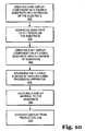
- FIG. 9shows one method of assembling a flexible display along the length of a flexible substrate 70 in accordance with an embodiment of the invention.
- blocksare assembled into the openings of the flexible substrate.
- a plurality of blocksare deposited in a slurry that go into the recessed regions of the flexible substrate.
- Planarization of the assembly of blocks into substrate 72is the next step. Planarization takes place by depositing a material that may be spun to flatten or may be subjected to conventional chemical-mechanical polishing.
- the electrical coupling of the plurality of blockstakes place at step 74 by opening holes in the planarization layer and depositing metalization material or other conductive materials into the holes and beyond the holes to form an interconnect (e.g., a row or column interconnect).
- the interconnect between the rows and columnsis comprised of flexible and conductive material.
- the interconnectcould be made of conductive polymers, metals (e.g., aluminum, copper, silver, gold, etc.), metal particles, conductive organic compounds, or conductive oxides.
- the displayis made to conform the object's shape 78 . It should be noted that the operations for forming the display may be done in a different order than that found in FIG. 9 and thus the operation 78 may be performed after operation 80 .
- a display generation substratee.g., a PDLC layer
- a display generation substrateis coupled to the active matrix backplane 80 .
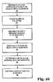
- FIG. 10shows a method of manufacturing multiple displays along a flexible substrate.
- Multiple display componentsare created on a flexible substrate 200 .
- the flexible substrateis advanced to a second region on the substrate 202 .
- a new display componentis created on the flexible substrate in a different region of the substrate 204 by advancing the flexible substrate through a web processing of apparatus 206 and coupling a display material to the substrate 208 . Separation of the display panel occurs at the end of the process 210 .
- FIG. 11shows a flexible substrate with multiple display components.
- the flexible substrate 220has display component 222 and display component 224 attached thereto.
- the substratehas three lengths: a first length 226 , a second length 228 , and a third length 230 .
- Display components 222 and 224are active matrix display devices.
- FIG. 12Ashows display component 222 that has a passive matrix display backplane attached thereto.
- FIG. 12Bshows a display component 224 that has an active matrix display backplane attached thereto.
- FIG. 13shows a flexible substrate 50 attached to a display backplane.
- FIG. 14Ashows a reflective display backplane 48 coupled to a flexible substrate 46 .
- FIG. 14Bshows a flexible reflective display backplane 48 coupled to a substrate 46 .
- Blocks 14are coupled to the flexible substrate 46 and to the flexible reflective display backplane 48 .
- the reflective display backplaneincludes an interconnect layer 45 .
- This interconnect layer 45typically is comprised of metallic material. Coupled to the flexible substrate is a flexible reflector 48 .
- FIG. 14Cshows a flexible reflective display wherein recessed region 45 contains reflective material 44 .
- the substrate 46is coupled to the reflective display backplane 48 .
- FIG. 15Ashows a method of fabricating a display device wherein a flexible substrate and a display tape undergo processing and are subsequently coupled.
- the flexible substrateis advanced along a process line 500 .
- a slurry containing a plurality of blocksis dispensed onto the flexible substrate 502 .
- a second slurry containing a plurality of blocksis again dispensed onto the substrate. Excess slurry is collected in a container and is recycled. The blocks fall into recessed regions in the substrate.
- Adhesives and spacersare deposited onto the substrate 504 .
- Display materialis placed onto the substrate 508 . This material may comprise polymer-dispersed liquid crystal, cholesteric liquid crystal, electrophoretic liquid crystal, upconverting phosphor, or downconverting phosphor 512 .
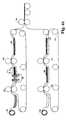
- FIG. 15Bshows the overall process of fabricating a display device wherein a flexible substrate 120 and a display tape 160 undergo processing and are subsequently coupled.
- the flexible substrateis advanced along a first process line and advances through a first set of support members 122 .
- a first slurry 124 containing a plurality of blocksis dispensed onto the flexible substrate.
- a second slurry 126 containing a plurality of blocksis again dispensed onto the substrate. Excess slurry is collected in a container 128 and is recycled. The blocks fall into recessed regions in the substrate.
- a polarizing or retarding filmcould be deposited onto the substrate before the FSA process is applied to the substrate.
- Flexible substrate 120is advanced through a second set of support members 130 .
- Display tape 160undergoes a separate process.
- Display materialis placed onto at least one side of the display tape 160 .
- Display tape 160is advanced through a first set of support members 164 .
- the display materialis patterned or layered 168 .
- This display materialmay comprise polymer-dispersed liquid crystal, cholesteric liquid crystal, electrophoretic liquid crystal, upconverting phosphor, or downconverting phosphor.
- Display tape 160is advanced through a second set of support members 170 .
- An interconnect 172is either deposited or etched onto the display tape 160 .
- the display tapeis then advanced to point 134 where the display tape is coupled to the substrate.
- a conveyor belt 174surrounds the support members.
- FIG. 16relates to a method of picking and placing of objects onto a flexible substrate after the FSA process has been applied to the substrate.
- a slurry containing a plurality of objectsis dispensed onto the substrate 90 .
- the objectsfall into recessed regions in the substrate.
- the excess slurryis collected and recycled 91 .
- the substrateis checked for empty recessed regions 92 . This checking is performed by an electronic eye that views the substrate.
- Objectsare robotically placed into empty regions found in substrate 94 .
- a metalization materialis placed onto at least one of the substrate's surfaces and is patterned or etched 96 .
- the display tapeis coupled to the substrate 98 .
- FIG. 17relates to the FSA process and the coupling of the display material with the substrate.
- a slurry containing a plurality of blocksis deposited onto the substrate 400 . If the recessed regions are of equivalent size, step 450 is then followed. If not, a first slurry with a first plurality of objects is deposited onto the substrate 410 . Excess slurry is caught and recycled 415 . Once this step is performed, a second slurred with a second plurality of objects is placed onto the substrate 420 . Excess second slurry is recycled into a second container 425 . A metal interconnect is then deposited onto the substrate 435 . After these steps, a display material is deposited onto the substrate 430 .
- FIG. 18shows a flexible continuous substrate wherein two displays are created.
- Display device 52is larger than display device 50 . This shows that multiple displays of different sizes can be created on the substrate through an in-line process.
- FIG. 19shows displays 54 and 56 of similar size.
- the substrateitself may have different sized recessed regions. This allows the substrate to receive various sized blocks or devices.
- FIG. 20shows a cross-sectional view of the recessed regions in the substrate. Recessed region 65 is smaller than recessed region 67 .
- FIG. 21shows an embodiment of the overall in-line process of the invention.
- a web apparatus machine 119is used to process the substrate.
- aperturesare created in the flexible substrate. These apertures can be created by a number of methods. For example, the apertures can be punched into the substrate. Another method involves using a template to create the apertures. A laser, chemical or plasma etching could also be used to create the apertures.
- the substrateadvances over a plurality of support members 122 .
- the substrategoes in between support members 123 and 123 B.
- the FSA processis applied to the substrate.
- FSAcomprises a slurry that contains a plurality of functional blocks. These blocks have, in one embodiment, a circuit element (not shown) that drives the picture element (not shown).
- the FSA processoccurs at block 124 . It is then applied again at 126 . The excess slurry is collected in container 128 . Then, the flexible substrate advances through support members 130 . The flexible substrate then has an interconnect 131 deposited on the top of the flexible substrate 132 . The resulting flexible substrate advances over a guide member and meets at a point 134 wherein it is coupled to a display tape that in one embodiment is a flexible substrate that includes separate regions each having a display material on this flexible substrate. A different portion of the process involves the display tape 160 . Before the display tape is coupled with the substrate, the display tape goes through its own separate process that is described below.
- the display tapehas display material 162 deposited on at least one side of the display tape.
- display materialmay be deposited onto the display tape.
- display materialmay be sprayed onto the display tape.
- the display materialalso may be placed on a screen over the display tape.
- Another methodis to place the display tape into a container that holds the display material.
- the display tapeadvances through support members 164 .
- the display tapethen has display material layered or patterned on the display tape at 168 .
- This display tapethen advances through another plurality of support members 170 .
- a large area metal interconnectis then deposited or etched onto the display tape 172 . This may be performed by inkjet, lithography and etch, screen print, laser etch, or deposit 174 . In one embodiment of the invention, this large interconnect is a cover glass electrode.
- the display tapeis coupled with a substrate.
- FIG. 22shows a display material being placed through a screen 180 onto display tape 168 .
- the screen 180has a desired pattern created by holes that go through the screen 180 . This desired pattern may be dictated by a customer or by the manufacturer.
- FIG. 23shows a top view of display material being laser etched onto display tape 168 .
- the etchingoccurs when the high intensity light from the laser 182 strikes the display material on top of the display tape 168 .
- a patternis created in the display material by the laser 182 .
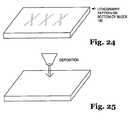
- FIG. 24shows lithography being used to pattern the display material. Lithography involves using a block 183 with a pattern engraved in the bottom surface of the block 183 . The bottom surface of the block 183 contacts the display material.
- FIG. 25shows yet another method of depositing display material onto the display tape.
- There display materialis deposited in a pattern onto the display tape 168 .
- the display materialis deposited by a container 183 that contains the display material.
- the container 183is placed over the display tape 168 .
- the display materialdrops onto the display tape 168 in a pattern.
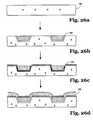
- FIGS. 26A-26Dshows generally the process of planarization material being added onto the substrate.
- FIG. 26Ashows a planar side view of a substrate 190 .
- FIG. 26Bshows openings or receptor regions 192 created and blocks deposited into the substrate.
- FIG. 26Cshows deposition of planarization material 194 and openings being created into the substrate.
- FIG. 26Dshows deposition of interconnect 198 and pattern interconnect.
- an array of componentse.g. display components
- an array of other assembliessuch as x-ray detectors, radar detectors, micro-electro-mechanical structural elements (MEMS) or, generally, an assembly of sensors or actuators or an assembly of circuit elements also may be produced using the claimed invention.
- MEMSmicro-electro-mechanical structural elements
- flexible antennas, other sensors, detectors, or an array of circuit elementsmay be fabricated using one of the embodiments of the inventions.
- Other aspects and methods of the present invention as well as apparatuses formed using these methodsare described further below in conjunction with the following figures.
Landscapes
- Engineering & Computer Science (AREA)
- Microelectronics & Electronic Packaging (AREA)
- Computer Hardware Design (AREA)
- Power Engineering (AREA)
- Physics & Mathematics (AREA)
- General Physics & Mathematics (AREA)
- Nonlinear Science (AREA)
- Chemical & Material Sciences (AREA)
- Crystallography & Structural Chemistry (AREA)
- Mathematical Physics (AREA)
- Optics & Photonics (AREA)
- Manufacturing & Machinery (AREA)
- Condensed Matter Physics & Semiconductors (AREA)
- Devices For Indicating Variable Information By Combining Individual Elements (AREA)
Abstract
Description
Claims (8)
Priority Applications (3)
| Application Number | Priority Date | Filing Date | Title |
|---|---|---|---|
| US10/812,788US6850312B2 (en) | 1999-03-16 | 2004-03-29 | Apparatuses and methods for flexible displays |
| US11/046,651US7113250B2 (en) | 1999-03-16 | 2005-01-28 | Apparatuses and methods for forming assemblies |
| US11/515,070US7561221B2 (en) | 1999-02-05 | 2006-09-01 | Apparatuses and methods for forming assemblies |
Applications Claiming Priority (3)
| Application Number | Priority Date | Filing Date | Title |
|---|---|---|---|
| US27014699A | 1999-03-16 | 1999-03-16 | |
| US09/932,505US7046328B2 (en) | 1999-02-05 | 2001-08-17 | Apparatuses and methods for flexible displays |
| US10/812,788US6850312B2 (en) | 1999-03-16 | 2004-03-29 | Apparatuses and methods for flexible displays |
Related Parent Applications (1)
| Application Number | Title | Priority Date | Filing Date |
|---|---|---|---|
| US09/932,505ContinuationUS7046328B2 (en) | 1999-02-05 | 2001-08-17 | Apparatuses and methods for flexible displays |
Related Child Applications (1)
| Application Number | Title | Priority Date | Filing Date |
|---|---|---|---|
| US11/046,651ContinuationUS7113250B2 (en) | 1999-02-05 | 2005-01-28 | Apparatuses and methods for forming assemblies |
Publications (2)
| Publication Number | Publication Date |
|---|---|
| US20040179145A1 US20040179145A1 (en) | 2004-09-16 |
| US6850312B2true US6850312B2 (en) | 2005-02-01 |
Family
ID=32965237
Family Applications (4)
| Application Number | Title | Priority Date | Filing Date |
|---|---|---|---|
| US10/812,788Expired - LifetimeUS6850312B2 (en) | 1999-02-05 | 2004-03-29 | Apparatuses and methods for flexible displays |
| US11/046,651Expired - LifetimeUS7113250B2 (en) | 1999-02-05 | 2005-01-28 | Apparatuses and methods for forming assemblies |
| US11/169,534Expired - Fee RelatedUS7172910B2 (en) | 1999-03-16 | 2005-06-28 | Web fabrication of devices |
| US11/515,070Expired - Fee RelatedUS7561221B2 (en) | 1999-02-05 | 2006-09-01 | Apparatuses and methods for forming assemblies |
Family Applications After (3)
| Application Number | Title | Priority Date | Filing Date |
|---|---|---|---|
| US11/046,651Expired - LifetimeUS7113250B2 (en) | 1999-02-05 | 2005-01-28 | Apparatuses and methods for forming assemblies |
| US11/169,534Expired - Fee RelatedUS7172910B2 (en) | 1999-03-16 | 2005-06-28 | Web fabrication of devices |
| US11/515,070Expired - Fee RelatedUS7561221B2 (en) | 1999-02-05 | 2006-09-01 | Apparatuses and methods for forming assemblies |
Country Status (1)
| Country | Link |
|---|---|
| US (4) | US6850312B2 (en) |
Cited By (74)
| Publication number | Priority date | Publication date | Assignee | Title |
|---|---|---|---|---|
| US20040188531A1 (en)* | 2003-03-24 | 2004-09-30 | Gengel Glenn W. | RFID tags and processes for producing RFID tags |
| US20050196524A1 (en)* | 1999-03-16 | 2005-09-08 | Jacobsen Jeffrey J. | Apparatuses and methods for forming assemblies |
| US20050238967A1 (en)* | 2004-04-27 | 2005-10-27 | The Board Of Trustees Of The University Of Illinois | Composite patterning devices for soft lithography |
| US20060109123A1 (en)* | 2004-11-22 | 2006-05-25 | Curt Carrender | Radio frequency identification (RFID) tag for an item having a conductive layer included or attached |
| US20060109130A1 (en)* | 2004-11-22 | 2006-05-25 | Hattick John B | Radio frequency identification (RFID) tag for an item having a conductive layer included or attached |
| US20060224263A1 (en)* | 2005-03-31 | 2006-10-05 | Semiconductor Energy Laboratory Co., Ltd. | Production system and production method |
| US20060255941A1 (en)* | 2005-05-11 | 2006-11-16 | Carrender Curtis L | Method and apparatus for testing RFID devices |
| US20060286785A1 (en)* | 2004-06-04 | 2006-12-21 | The Board Of Trustees Of The University Of Illinois | A Stretchable Form of Single Crystal Silicon for High Performance Electronics on Rubber Substrates |
| US20070032089A1 (en)* | 2004-06-04 | 2007-02-08 | The Board Of Trustees Of The University Of Illinois | Printable Semiconductor Structures and Related Methods of Making and Assembling |
| US20070256291A1 (en)* | 2001-05-31 | 2007-11-08 | Credelle Thomas L | Electronic devices with small functional elements supported on a carrier |
| WO2007131344A1 (en)* | 2006-05-16 | 2007-11-22 | Tribar Industries Inc. | Large scale flexible led video display and control system therefor |
| US20080055581A1 (en)* | 2004-04-27 | 2008-03-06 | Rogers John A | Devices and methods for pattern generation by ink lithography |
| US20080157235A1 (en)* | 2004-06-04 | 2008-07-03 | Rogers John A | Controlled buckling structures in semiconductor interconnects and nanomembranes for stretchable electronics |
| US20090033587A1 (en)* | 2007-07-31 | 2009-02-05 | Hewlett-Packard Development Company Lp | Display |
| US7557367B2 (en) | 2004-06-04 | 2009-07-07 | The Board Of Trustees Of The University Of Illinois | Stretchable semiconductor elements and stretchable electrical circuits |
| US20090320139A1 (en)* | 2004-11-22 | 2009-12-24 | Curt Carrender | Transponder incorporated into an electronic device |
| US20100052112A1 (en)* | 2008-04-03 | 2010-03-04 | Rogers John A | Printable, Flexible and Stretchable Diamond for Thermal Management |
| US20100068839A1 (en)* | 2007-05-31 | 2010-03-18 | Nthdegree Technologies Worldwide Inc. | Method of Manufacturing a Light Emitting, Photovoltaic or Other Electronic Apparatus and System |
| US20100087782A1 (en)* | 2008-10-07 | 2010-04-08 | Roozbeh Ghaffari | Catheter balloon having stretchable integrated circuitry and sensor array |
| US20100167441A1 (en)* | 2007-05-31 | 2010-07-01 | Nthdegree Technologies Worldwide Inc. | Method of Manufacturing a Light Emitting, Photovoltaic or Other Electronic Apparatus and System |
| US20100178722A1 (en)* | 2008-10-07 | 2010-07-15 | De Graff Bassel | Methods and applications of non-planar imaging arrays |
| US20100283069A1 (en)* | 2007-01-17 | 2010-11-11 | John Rogers | Optical systems fabricated by printing-based assembly |
| US20100298895A1 (en)* | 2008-10-07 | 2010-11-25 | Roozbeh Ghaffari | Systems, methods, and devices using stretchable or flexible electronics for medical applications |
| US20100317132A1 (en)* | 2009-05-12 | 2010-12-16 | Rogers John A | Printed Assemblies of Ultrathin, Microscale Inorganic Light Emitting Diodes for Deformable and Semitransparent Displays |
| US20110034912A1 (en)* | 2008-10-07 | 2011-02-10 | Mc10, Inc. | Systems,methods, and devices having stretchable integrated circuitry for sensing and delivering therapy |
| US7943491B2 (en) | 2004-06-04 | 2011-05-17 | The Board Of Trustees Of The University Of Illinois | Pattern transfer printing by kinetic control of adhesion to an elastomeric stamp |
| US20110147715A1 (en)* | 2008-06-16 | 2011-06-23 | Purdue Research Foundation | Medium Scale Carbon Nanotube Thin Film Integrated Circuits on Flexible Plastic Substrates |
| US20110218756A1 (en)* | 2009-10-01 | 2011-09-08 | Mc10, Inc. | Methods and apparatus for conformal sensing of force and/or acceleration at a person's head |
| US20110230747A1 (en)* | 2010-03-17 | 2011-09-22 | Rogers John A | Implantable biomedical devices on bioresorbable substrates |
| US8182303B2 (en) | 2004-12-27 | 2012-05-22 | Nthdegree Technologies Worldwide Inc | Method of fabricating static and addressable emissive displays |
| US8367035B2 (en) | 2006-03-03 | 2013-02-05 | The Board Of Trustees Of The University Of Illinois | Methods of making spatially aligned nanotubes and nanotube arrays |
| US8389862B2 (en) | 2008-10-07 | 2013-03-05 | Mc10, Inc. | Extremely stretchable electronics |
| US8413359B2 (en) | 2008-05-13 | 2013-04-09 | Nthdegree Technologies Worldwide Inc | Illuminating display systems |
| US8415879B2 (en) | 2007-05-31 | 2013-04-09 | Nthdegree Technologies Worldwide Inc | Diode for a printable composition |
| US8552299B2 (en) | 2008-03-05 | 2013-10-08 | The Board Of Trustees Of The University Of Illinois | Stretchable and foldable electronic devices |
| US20130277646A1 (en)* | 2012-04-19 | 2013-10-24 | Nobuyoshi Saito | Display panel and display device |
| US8674593B2 (en) | 2007-05-31 | 2014-03-18 | Nthdegree Technologies Worldwide Inc | Diode for a printable composition |
| US8739441B2 (en) | 2008-05-13 | 2014-06-03 | Nthdegree Technologies Worldwide Inc | Apparatuses for providing power for illumination of a display object |
| US8809126B2 (en) | 2007-05-31 | 2014-08-19 | Nthdegree Technologies Worldwide Inc | Printable composition of a liquid or gel suspension of diodes |
| US8846457B2 (en) | 2007-05-31 | 2014-09-30 | Nthdegree Technologies Worldwide Inc | Printable composition of a liquid or gel suspension of diodes |
| US8852467B2 (en) | 2007-05-31 | 2014-10-07 | Nthdegree Technologies Worldwide Inc | Method of manufacturing a printable composition of a liquid or gel suspension of diodes |
| US8877101B2 (en) | 2007-05-31 | 2014-11-04 | Nthdegree Technologies Worldwide Inc | Method of manufacturing a light emitting, power generating or other electronic apparatus |
| US8889216B2 (en) | 2007-05-31 | 2014-11-18 | Nthdegree Technologies Worldwide Inc | Method of manufacturing addressable and static electronic displays |
| US8934965B2 (en) | 2011-06-03 | 2015-01-13 | The Board Of Trustees Of The University Of Illinois | Conformable actively multiplexed high-density surface electrode array for brain interfacing |
| US9018833B2 (en) | 2007-05-31 | 2015-04-28 | Nthdegree Technologies Worldwide Inc | Apparatus with light emitting or absorbing diodes |
| US9159635B2 (en) | 2011-05-27 | 2015-10-13 | Mc10, Inc. | Flexible electronic structure |
| US9171794B2 (en) | 2012-10-09 | 2015-10-27 | Mc10, Inc. | Embedding thin chips in polymer |
| US9343593B2 (en) | 2007-05-31 | 2016-05-17 | Nthdegree Technologies Worldwide Inc | Printable composition of a liquid or gel suspension of diodes |
| US9419179B2 (en) | 2007-05-31 | 2016-08-16 | Nthdegree Technologies Worldwide Inc | Diode for a printable composition |
| US9425357B2 (en) | 2007-05-31 | 2016-08-23 | Nthdegree Technologies Worldwide Inc. | Diode for a printable composition |
| US9442285B2 (en) | 2011-01-14 | 2016-09-13 | The Board Of Trustees Of The University Of Illinois | Optical component array having adjustable curvature |
| US9534772B2 (en) | 2007-05-31 | 2017-01-03 | Nthdegree Technologies Worldwide Inc | Apparatus with light emitting diodes |
| US9554484B2 (en) | 2012-03-30 | 2017-01-24 | The Board Of Trustees Of The University Of Illinois | Appendage mountable electronic devices conformable to surfaces |
| US20170133558A1 (en)* | 2014-10-31 | 2017-05-11 | eLux Inc. | System and Method for the Fluidic Assembly of Emissive Displays |
| US20170140961A1 (en)* | 2014-10-31 | 2017-05-18 | eLux Inc. | Pick-and-Remove System and Method for Emissive Display Repair |
| US9691873B2 (en) | 2011-12-01 | 2017-06-27 | The Board Of Trustees Of The University Of Illinois | Transient devices designed to undergo programmable transformations |
| US9723122B2 (en) | 2009-10-01 | 2017-08-01 | Mc10, Inc. | Protective cases with integrated electronics |
| US9765934B2 (en) | 2011-05-16 | 2017-09-19 | The Board Of Trustees Of The University Of Illinois | Thermally managed LED arrays assembled by printing |
| US9825202B2 (en) | 2014-10-31 | 2017-11-21 | eLux, Inc. | Display with surface mount emissive elements |
| US9936574B2 (en) | 2009-12-16 | 2018-04-03 | The Board Of Trustees Of The University Of Illinois | Waterproof stretchable optoelectronics |
| US10236279B2 (en) | 2014-10-31 | 2019-03-19 | eLux, Inc. | Emissive display with light management system |
| US10242977B2 (en) | 2014-10-31 | 2019-03-26 | eLux, Inc. | Fluid-suspended microcomponent harvest, distribution, and reclamation |
| US10319878B2 (en) | 2014-10-31 | 2019-06-11 | eLux, Inc. | Stratified quantum dot phosphor structure |
| US10381335B2 (en) | 2014-10-31 | 2019-08-13 | ehux, Inc. | Hybrid display using inorganic micro light emitting diodes (uLEDs) and organic LEDs (OLEDs) |
| US10381332B2 (en) | 2014-10-31 | 2019-08-13 | eLux Inc. | Fabrication method for emissive display with light management system |
| US10441185B2 (en) | 2009-12-16 | 2019-10-15 | The Board Of Trustees Of The University Of Illinois | Flexible and stretchable electronic systems for epidermal electronics |
| US10520769B2 (en) | 2014-10-31 | 2019-12-31 | eLux, Inc. | Emissive display with printed light modification structures |
| US10535640B2 (en) | 2014-10-31 | 2020-01-14 | eLux Inc. | System and method for the fluidic assembly of micro-LEDs utilizing negative pressure |
| US10543486B2 (en) | 2014-10-31 | 2020-01-28 | eLux Inc. | Microperturbation assembly system and method |
| US10918298B2 (en) | 2009-12-16 | 2021-02-16 | The Board Of Trustees Of The University Of Illinois | High-speed, high-resolution electrophysiology in-vivo using conformal electronics |
| US10925543B2 (en) | 2015-11-11 | 2021-02-23 | The Board Of Trustees Of The University Of Illinois | Bioresorbable silicon electronics for transient implants |
| US11029198B2 (en) | 2015-06-01 | 2021-06-08 | The Board Of Trustees Of The University Of Illinois | Alternative approach for UV sensing |
| US11118965B2 (en) | 2015-06-01 | 2021-09-14 | The Board Of Trustees Of The University Of Illinois | Miniaturized electronic systems with wireless power and near-field communication capabilities |
| US11903187B2 (en) | 2021-04-30 | 2024-02-13 | Samsung Electronics Co., Ltd. | Semiconductor devices |
Families Citing this family (33)
| Publication number | Priority date | Publication date | Assignee | Title |
|---|---|---|---|---|
| US6479395B1 (en)* | 1999-11-02 | 2002-11-12 | Alien Technology Corporation | Methods for forming openings in a substrate and apparatuses with these openings and methods for creating assemblies with openings |
| US6623579B1 (en)* | 1999-11-02 | 2003-09-23 | Alien Technology Corporation | Methods and apparatus for fluidic self assembly |
| EP1243032B1 (en)* | 1999-12-21 | 2019-11-20 | Flexenable Limited | Inkjet-fabricated integrated circuits |
| US6780696B1 (en)* | 2000-09-12 | 2004-08-24 | Alien Technology Corporation | Method and apparatus for self-assembly of functional blocks on a substrate facilitated by electrode pairs |
| US6863219B1 (en)* | 2001-08-17 | 2005-03-08 | Alien Technology Corporation | Apparatuses and methods for forming electronic assemblies |
| US20060055691A1 (en)* | 2004-09-11 | 2006-03-16 | Bursett Jeffrey M | Attachable informational appliance |
| US7452748B1 (en) | 2004-11-08 | 2008-11-18 | Alien Technology Corporation | Strap assembly comprising functional block deposited therein and method of making same |
| CN100517645C (en)* | 2005-01-24 | 2009-07-22 | 松下电器产业株式会社 | Manufacturing method of semiconductor chip and semiconductor chip |
| US8334819B2 (en)* | 2005-03-11 | 2012-12-18 | The Invention Science Fund I, Llc | Superimposed displays |
| US9153163B2 (en)* | 2005-03-11 | 2015-10-06 | The Invention Science Fund I, Llc | Self assembly of elements for displays |
| US7990349B2 (en)* | 2005-04-22 | 2011-08-02 | The Invention Science Fund I, Llc | Superimposed displays |
| US8390537B2 (en)* | 2005-03-11 | 2013-03-05 | The Invention Science Fund I, Llc | Method of assembling displays on substrates |
| US8711063B2 (en) | 2005-03-11 | 2014-04-29 | The Invention Science Fund I, Llc | Self assembly of elements for displays |
| US8300007B2 (en)* | 2005-03-11 | 2012-10-30 | The Invention Science Fund I, Llc | Self assembling display with substrate |
| US7662008B2 (en)* | 2005-04-04 | 2010-02-16 | Searete Llc | Method of assembling displays on substrates |
| US7977130B2 (en)* | 2006-08-03 | 2011-07-12 | The Invention Science Fund I, Llc | Method of assembling displays on substrates |
| US20060202944A1 (en)* | 2005-03-11 | 2006-09-14 | Searete Llc, A Limited Liability Corporation Of The State Of Delaware | Elements for self assembling displays |
| US8860635B2 (en)* | 2005-04-04 | 2014-10-14 | The Invention Science Fund I, Llc | Self assembling display with substrate |
| US20070082464A1 (en)* | 2005-10-11 | 2007-04-12 | Schatz Kenneth D | Apparatus for block assembly process |
| US20070085838A1 (en)* | 2005-10-17 | 2007-04-19 | Ricks Theodore K | Method for making a display with integrated touchscreen |
| US20070096646A1 (en)* | 2005-10-28 | 2007-05-03 | Van Nice Harold L | Electroluminescent displays |
| US8020475B2 (en)* | 2006-06-02 | 2011-09-20 | Kent Displays Incorporated | Method of simultaneous singulation and edge sealing of plastic displays |
| US9209059B2 (en)* | 2009-12-17 | 2015-12-08 | Cooledge Lighting, Inc. | Method and eletrostatic transfer stamp for transferring semiconductor dice using electrostatic transfer printing techniques |
| US20110191150A1 (en)* | 2010-01-29 | 2011-08-04 | Bank Of America Corporation | Mobile integrated merchant offer program and customer shopping using product level information |
| EP2999989A4 (en) | 2013-05-22 | 2017-01-04 | Clearink Displays, Inc. | Method and apparatus for improved color filter saturation |
| US10705404B2 (en) | 2013-07-08 | 2020-07-07 | Concord (Hk) International Education Limited | TIR-modulated wide viewing angle display |
| CN105097680B (en) | 2014-05-16 | 2019-06-07 | 恩智浦美国有限公司 | Protectiveness for integrated circuit device encapsulates |
| CN107111016B (en) | 2014-10-08 | 2020-08-28 | 协和(香港)国际教育有限公司 | Color filter aligned reflective display |
| US10386691B2 (en) | 2015-06-24 | 2019-08-20 | CLEARink Display, Inc. | Method and apparatus for a dry particle totally internally reflective image display |
| US10261221B2 (en) | 2015-12-06 | 2019-04-16 | Clearink Displays, Inc. | Corner reflector reflective image display |
| US10386547B2 (en) | 2015-12-06 | 2019-08-20 | Clearink Displays, Inc. | Textured high refractive index surface for reflective image displays |
| WO2019032905A1 (en)* | 2017-08-11 | 2019-02-14 | Clearink Displays, Inc. | System, method and apparatus for flexible tir-based image displays |
| US10615230B2 (en)* | 2017-11-08 | 2020-04-07 | Teradyne, Inc. | Identifying potentially-defective picture elements in an active-matrix display panel |
Citations (16)
| Publication number | Priority date | Publication date | Assignee | Title |
|---|---|---|---|---|
| US3439416A (en)* | 1966-02-03 | 1969-04-22 | Gen Telephone & Elect | Method and apparatus for fabricating an array of discrete elements |
| US4191800A (en)* | 1976-05-27 | 1980-03-04 | Bell Telephone Laboratories, Incorporated | Devices employing flexible substrates and method for making same |
| US4514583A (en)* | 1983-11-07 | 1985-04-30 | Energy Conversion Devices, Inc. | Substrate for photovoltaic devices |
| US4966442A (en)* | 1988-02-02 | 1990-10-30 | Seiko Epson Corporation | Electro-optical device and method for manufacturing same |
| US5034802A (en) | 1989-12-11 | 1991-07-23 | Hewlett-Packard Company | Mechanical simultaneous registration of multi-pin surface-mount components to sites on substrates |
| US5436744A (en)* | 1993-09-03 | 1995-07-25 | Motorola Inc. | Flexible liquid crystal display with integrated driver circuit and display electrodes formed on opposite sides of folded substrate |
| US5453864A (en)* | 1990-02-16 | 1995-09-26 | Seiko Epson Corporation | Liquid crystal element and electronic apparatus |
| US5545291A (en)* | 1993-12-17 | 1996-08-13 | The Regents Of The University Of California | Method for fabricating self-assembling microstructures |
| EP0747948A2 (en) | 1995-06-07 | 1996-12-11 | The Regents Of The University Of California | Method and apparatus for fabricating self-assembling microstructures |
| US5904545A (en) | 1993-12-17 | 1999-05-18 | The Regents Of The University Of California | Apparatus for fabricating self-assembling microstructures |
| WO1999067678A2 (en) | 1998-06-22 | 1999-12-29 | E-Ink Corporation | Means of addressing microencapsulated display media |
| US6274508B1 (en)* | 1999-02-05 | 2001-08-14 | Alien Technology Corporation | Apparatuses and methods used in forming assemblies |
| US6281038B1 (en)* | 1999-02-05 | 2001-08-28 | Alien Technology Corporation | Methods for forming assemblies |
| US20010031514A1 (en)* | 1993-12-17 | 2001-10-18 | Smith John Stephen | Method and apparatus for fabricating self-assembling microstructures |
| US6316278B1 (en)* | 1999-03-16 | 2001-11-13 | Alien Technology Corporation | Methods for fabricating a multiple modular assembly |
| US6468638B2 (en)* | 1999-03-16 | 2002-10-22 | Alien Technology Corporation | Web process interconnect in electronic assemblies |
Family Cites Families (11)
| Publication number | Priority date | Publication date | Assignee | Title |
|---|---|---|---|---|
| EP0647091A1 (en)* | 1993-10-05 | 1995-04-05 | AT&T Corp. | Passive alignment of components with micromachined tool |
| JP3109968B2 (en) | 1994-12-12 | 2000-11-20 | キヤノン株式会社 | Method for manufacturing active matrix circuit board and method for manufacturing liquid crystal display device using the circuit board |
| US5775569A (en)* | 1996-10-31 | 1998-07-07 | Ibm Corporation | Method for building interconnect structures by injection molded solder and structures built |
| US6507989B1 (en)* | 1997-03-13 | 2003-01-21 | President And Fellows Of Harvard College | Self-assembly of mesoscale objects |
| US6094138A (en)* | 1998-02-27 | 2000-07-25 | Motorola, Inc. | Integrated circuit assembly and method of assembly |
| US6091332A (en)* | 1998-06-09 | 2000-07-18 | Motorola, Inc. | Radio frequency identification tag having printed circuit interconnections |
| US6246327B1 (en)* | 1998-06-09 | 2001-06-12 | Motorola, Inc. | Radio frequency identification tag circuit chip having printed interconnection pads |
| US6514618B1 (en)* | 1998-11-06 | 2003-02-04 | Acoustic Imaging Technologies Corp. | Multilayer backing material for 2-D ultrasonic imaging arrays |
| WO2000046854A1 (en)* | 1999-02-05 | 2000-08-10 | Alien Technology Corporation | Apparatuses and methods for forming assemblies |
| US6850312B2 (en)* | 1999-03-16 | 2005-02-01 | Alien Technology Corporation | Apparatuses and methods for flexible displays |
| US6426564B1 (en)* | 1999-02-24 | 2002-07-30 | Micron Technology, Inc. | Recessed tape and method for forming a BGA assembly |
- 2004
- 2004-03-29USUS10/812,788patent/US6850312B2/ennot_activeExpired - Lifetime
- 2005
- 2005-01-28USUS11/046,651patent/US7113250B2/ennot_activeExpired - Lifetime
- 2005-06-28USUS11/169,534patent/US7172910B2/ennot_activeExpired - Fee Related
- 2006
- 2006-09-01USUS11/515,070patent/US7561221B2/ennot_activeExpired - Fee Related
Patent Citations (16)
| Publication number | Priority date | Publication date | Assignee | Title |
|---|---|---|---|---|
| US3439416A (en)* | 1966-02-03 | 1969-04-22 | Gen Telephone & Elect | Method and apparatus for fabricating an array of discrete elements |
| US4191800A (en)* | 1976-05-27 | 1980-03-04 | Bell Telephone Laboratories, Incorporated | Devices employing flexible substrates and method for making same |
| US4514583A (en)* | 1983-11-07 | 1985-04-30 | Energy Conversion Devices, Inc. | Substrate for photovoltaic devices |
| US4966442A (en)* | 1988-02-02 | 1990-10-30 | Seiko Epson Corporation | Electro-optical device and method for manufacturing same |
| US5034802A (en) | 1989-12-11 | 1991-07-23 | Hewlett-Packard Company | Mechanical simultaneous registration of multi-pin surface-mount components to sites on substrates |
| US5453864A (en)* | 1990-02-16 | 1995-09-26 | Seiko Epson Corporation | Liquid crystal element and electronic apparatus |
| US5436744A (en)* | 1993-09-03 | 1995-07-25 | Motorola Inc. | Flexible liquid crystal display with integrated driver circuit and display electrodes formed on opposite sides of folded substrate |
| US20010031514A1 (en)* | 1993-12-17 | 2001-10-18 | Smith John Stephen | Method and apparatus for fabricating self-assembling microstructures |
| US5545291A (en)* | 1993-12-17 | 1996-08-13 | The Regents Of The University Of California | Method for fabricating self-assembling microstructures |
| US5904545A (en) | 1993-12-17 | 1999-05-18 | The Regents Of The University Of California | Apparatus for fabricating self-assembling microstructures |
| EP0747948A2 (en) | 1995-06-07 | 1996-12-11 | The Regents Of The University Of California | Method and apparatus for fabricating self-assembling microstructures |
| WO1999067678A2 (en) | 1998-06-22 | 1999-12-29 | E-Ink Corporation | Means of addressing microencapsulated display media |
| US6274508B1 (en)* | 1999-02-05 | 2001-08-14 | Alien Technology Corporation | Apparatuses and methods used in forming assemblies |
| US6281038B1 (en)* | 1999-02-05 | 2001-08-28 | Alien Technology Corporation | Methods for forming assemblies |
| US6316278B1 (en)* | 1999-03-16 | 2001-11-13 | Alien Technology Corporation | Methods for fabricating a multiple modular assembly |
| US6468638B2 (en)* | 1999-03-16 | 2002-10-22 | Alien Technology Corporation | Web process interconnect in electronic assemblies |
Non-Patent Citations (3)
| Title |
|---|
| Nakamura, Eiji, et al.; 37.3: Development Of Electrophoretic Display Using Microcapsulated Suspension; SID International Symposium Digest Of Technical Papers, US, Santa Ana, CA.; SID vol. 29, 1998; pp. 1014-1017. |
| Search Report for PCT/US 99/30391 mailed May 23, 2000; 5 pages. |
| Wu, C.C.; Integration of Organic LED's and Amorphous Si TFT's onto Flexible and Lightweight Metal Foil Substrates; IEEE Electron Device Letters, US, IEEE Inc., New York; vol. 18, No. 12, Dec. 1, 1997; pp. 609-612. |
Cited By (192)
| Publication number | Priority date | Publication date | Assignee | Title |
|---|---|---|---|---|
| US7561221B2 (en) | 1999-02-05 | 2009-07-14 | Alien Technology Corporation | Apparatuses and methods for forming assemblies |
| US20070002203A1 (en)* | 1999-02-05 | 2007-01-04 | Jacobsen Jeffrey J | Apparatuses and methods for forming assemblies |
| US7113250B2 (en) | 1999-03-16 | 2006-09-26 | Alien Technology Corporation | Apparatuses and methods for forming assemblies |
| US20050196524A1 (en)* | 1999-03-16 | 2005-09-08 | Jacobsen Jeffrey J. | Apparatuses and methods for forming assemblies |
| US7559131B2 (en) | 2001-05-31 | 2009-07-14 | Alien Technology Corporation | Method of making a radio frequency identification (RFID) tag |
| US8516683B2 (en) | 2001-05-31 | 2013-08-27 | Alien Technology Corporation | Methods of making a radio frequency identification (RFID) tags |
| US20070256291A1 (en)* | 2001-05-31 | 2007-11-08 | Credelle Thomas L | Electronic devices with small functional elements supported on a carrier |
| US20090271973A1 (en)* | 2001-05-31 | 2009-11-05 | Thomas Lloyd Credelle | Methods of Making a Radio Frequency Identification (RFID) Tags |
| US20060267778A1 (en)* | 2003-03-24 | 2006-11-30 | Gengel Gleen W | RFID tags and processes for producing RFID tags |
| US7489248B2 (en) | 2003-03-24 | 2009-02-10 | Alien Technology Corporation | RFID tags and processes for producing RFID tags |
| US7253735B2 (en) | 2003-03-24 | 2007-08-07 | Alien Technology Corporation | RFID tags and processes for producing RFID tags |
| US7868766B2 (en) | 2003-03-24 | 2011-01-11 | Alien Technology Corporation | RFID tags and processes for producing RFID tags |
| US9418328B2 (en) | 2003-03-24 | 2016-08-16 | Ruizhang Technology Limited Company | RFID tags and processes for producing RFID tags |
| US20040188531A1 (en)* | 2003-03-24 | 2004-09-30 | Gengel Glenn W. | RFID tags and processes for producing RFID tags |
| US8912907B2 (en) | 2003-03-24 | 2014-12-16 | Alien Technology, Llc | RFID tags and processes for producing RFID tags |
| US20090167534A1 (en)* | 2003-03-24 | 2009-07-02 | Gengel Glenn W | Rfid tags and processes for producing rfid tags |
| US8350703B2 (en) | 2003-03-24 | 2013-01-08 | Alien Technology Corporation | RFID tags and processes for producing RFID tags |
| US20050238967A1 (en)* | 2004-04-27 | 2005-10-27 | The Board Of Trustees Of The University Of Illinois | Composite patterning devices for soft lithography |
| US7195733B2 (en) | 2004-04-27 | 2007-03-27 | The Board Of Trustees Of The University Of Illinois | Composite patterning devices for soft lithography |
| US20080055581A1 (en)* | 2004-04-27 | 2008-03-06 | Rogers John A | Devices and methods for pattern generation by ink lithography |
| US8217381B2 (en) | 2004-06-04 | 2012-07-10 | The Board Of Trustees Of The University Of Illinois | Controlled buckling structures in semiconductor interconnects and nanomembranes for stretchable electronics |
| US12074213B2 (en) | 2004-06-04 | 2024-08-27 | The Board Of Trustees Of The University Of Illinois | Methods and devices for fabricating and assembling printable semiconductor elements |
| US9105555B2 (en) | 2004-06-04 | 2015-08-11 | The Board Of Trustees Of The University Of Illinois | Stretchable form of single crystal silicon for high performance electronics on rubber substrates |
| US7521292B2 (en) | 2004-06-04 | 2009-04-21 | The Board Of Trustees Of The University Of Illinois | Stretchable form of single crystal silicon for high performance electronics on rubber substrates |
| US20080157235A1 (en)* | 2004-06-04 | 2008-07-03 | Rogers John A | Controlled buckling structures in semiconductor interconnects and nanomembranes for stretchable electronics |
| US7982296B2 (en) | 2004-06-04 | 2011-07-19 | The Board Of Trustees Of The University Of Illinois | Methods and devices for fabricating and assembling printable semiconductor elements |
| US8394706B2 (en) | 2004-06-04 | 2013-03-12 | The Board Of Trustees Of The University Of Illinois | Printable semiconductor structures and related methods of making and assembling |
| US7557367B2 (en) | 2004-06-04 | 2009-07-07 | The Board Of Trustees Of The University Of Illinois | Stretchable semiconductor elements and stretchable electrical circuits |
| US20070032089A1 (en)* | 2004-06-04 | 2007-02-08 | The Board Of Trustees Of The University Of Illinois | Printable Semiconductor Structures and Related Methods of Making and Assembling |
| US20060286785A1 (en)* | 2004-06-04 | 2006-12-21 | The Board Of Trustees Of The University Of Illinois | A Stretchable Form of Single Crystal Silicon for High Performance Electronics on Rubber Substrates |
| US8440546B2 (en) | 2004-06-04 | 2013-05-14 | The Board Of Trustees Of The University Of Illinois | Methods and devices for fabricating and assembling printable semiconductor elements |
| US7622367B1 (en) | 2004-06-04 | 2009-11-24 | The Board Of Trustees Of The University Of Illinois | Methods and devices for fabricating and assembling printable semiconductor elements |
| US20090294803A1 (en)* | 2004-06-04 | 2009-12-03 | The Board Of Trustees Of The University Of Illinois | Methods and devices for fabricating and assembling printable semiconductor elements |
| US8198621B2 (en) | 2004-06-04 | 2012-06-12 | The Board Of Trustees Of The University Of Illinois | Stretchable form of single crystal silicon for high performance electronics on rubber substrates |
| US8754396B2 (en) | 2004-06-04 | 2014-06-17 | The Board Of Trustees Of The University Of Illinois | Stretchable form of single crystal silicon for high performance electronics on rubber substrates |
| US9324733B2 (en) | 2004-06-04 | 2016-04-26 | The Board Of Trustees Of The University Of Illinois | Controlled buckling structures in semiconductor interconnects and nanomembranes for stretchable electronics |
| US20100059863A1 (en)* | 2004-06-04 | 2010-03-11 | The Board Of Trustees Of The University Of Illinois | Stretchable Form of Single Crystal Silicon for High Performance Electronics on Rubber Substrates |
| US11456258B2 (en) | 2004-06-04 | 2022-09-27 | The Board Of Trustees Of The University Of Illinois | Stretchable form of single crystal silicon for high performance electronics on rubber substrates |
| US20100072577A1 (en)* | 2004-06-04 | 2010-03-25 | The Board Of Trustees Of The University Of Illinois | Methods and Devices for Fabricating and Assembling Printable Semiconductor Elements |
| US8664699B2 (en) | 2004-06-04 | 2014-03-04 | The Board Of Trustees Of The University Of Illinois | Methods and devices for fabricating and assembling printable semiconductor elements |
| US9450043B2 (en) | 2004-06-04 | 2016-09-20 | The Board Of Trustees Of The University Of Illinois | Methods and devices for fabricating and assembling printable semiconductor elements |
| US11088268B2 (en) | 2004-06-04 | 2021-08-10 | The Board Of Trustees Of The University Of Illinois | Methods and devices for fabricating and assembling printable semiconductor elements |
| US9515025B2 (en) | 2004-06-04 | 2016-12-06 | The Board Of Trustees Of The University Of Illinois | Stretchable form of single crystal silicon for high performance electronics on rubber substrates |
| US7799699B2 (en) | 2004-06-04 | 2010-09-21 | The Board Of Trustees Of The University Of Illinois | Printable semiconductor structures and related methods of making and assembling |
| US8039847B2 (en) | 2004-06-04 | 2011-10-18 | The Board Of Trustees Of The University Of Illinois | Printable semiconductor structures and related methods of making and assembling |
| US9761444B2 (en) | 2004-06-04 | 2017-09-12 | The Board Of Trustees Of The University Of Illinois | Methods and devices for fabricating and assembling printable semiconductor elements |
| US10374072B2 (en) | 2004-06-04 | 2019-08-06 | The Board Of Trustees Of The University Of Illinois | Methods and devices for fabricating and assembling printable semiconductor elements |
| US8729524B2 (en) | 2004-06-04 | 2014-05-20 | The Board Of Trustees Of The University Of Illinois | Controlled buckling structures in semiconductor interconnects and nanomembranes for stretchable electronics |
| US9768086B2 (en) | 2004-06-04 | 2017-09-19 | The Board Of Trustees Of The University Of Illinois | Methods and devices for fabricating and assembling printable semiconductor elements |
| US7943491B2 (en) | 2004-06-04 | 2011-05-17 | The Board Of Trustees Of The University Of Illinois | Pattern transfer printing by kinetic control of adhesion to an elastomeric stamp |
| US10355113B2 (en) | 2004-06-04 | 2019-07-16 | The Board Of Trustees Of The University Of Illinois | Controlled buckling structures in semiconductor interconnects and nanomembranes for stretchable electronics |
| US10204864B2 (en) | 2004-06-04 | 2019-02-12 | The Board Of Trustees Of The University Of Illinois | Stretchable form of single crystal silicon for high performance electronics on rubber substrates |
| US7688206B2 (en) | 2004-11-22 | 2010-03-30 | Alien Technology Corporation | Radio frequency identification (RFID) tag for an item having a conductive layer included or attached |
| US20060109123A1 (en)* | 2004-11-22 | 2006-05-25 | Curt Carrender | Radio frequency identification (RFID) tag for an item having a conductive layer included or attached |
| US8471709B2 (en) | 2004-11-22 | 2013-06-25 | Alien Technology Corporation | Radio frequency identification (RFID) tag for an item having a conductive layer included or attached |
| US20060109130A1 (en)* | 2004-11-22 | 2006-05-25 | Hattick John B | Radio frequency identification (RFID) tag for an item having a conductive layer included or attached |
| US9070063B2 (en) | 2004-11-22 | 2015-06-30 | Ruizhang Technology Limited Company | Radio frequency identification (RFID) tag for an item having a conductive layer included or attached |
| US20090320139A1 (en)* | 2004-11-22 | 2009-12-24 | Curt Carrender | Transponder incorporated into an electronic device |
| US8183772B2 (en) | 2004-12-27 | 2012-05-22 | Nthdegree Technologies Worldwide Inc | Static and addressable emissive displays |
| US8182303B2 (en) | 2004-12-27 | 2012-05-22 | Nthdegree Technologies Worldwide Inc | Method of fabricating static and addressable emissive displays |
| US20060224263A1 (en)* | 2005-03-31 | 2006-10-05 | Semiconductor Energy Laboratory Co., Ltd. | Production system and production method |
| US8428761B2 (en) | 2005-03-31 | 2013-04-23 | Semiconductor Energy Laboratory Co., Ltd. | Production system and production method |
| US7659822B2 (en) | 2005-05-11 | 2010-02-09 | Alien Technology Corporation | Method and apparatus for testing RFID devices |
| US20060255941A1 (en)* | 2005-05-11 | 2006-11-16 | Carrender Curtis L | Method and apparatus for testing RFID devices |
| US7301458B2 (en) | 2005-05-11 | 2007-11-27 | Alien Technology Corporation | Method and apparatus for testing RFID devices |
| US7522055B2 (en) | 2005-05-11 | 2009-04-21 | Alien Technology Corporation | Method and apparatus for testing RFID devices |
| US20080117051A1 (en)* | 2005-05-11 | 2008-05-22 | Curtis Lee Carrender | Method and apparatus for testing rfid devices |
| US20080204244A1 (en)* | 2005-05-11 | 2008-08-28 | Curtis Lee Carrender | Method and apparatus for testing rfid devices |
| US8367035B2 (en) | 2006-03-03 | 2013-02-05 | The Board Of Trustees Of The University Of Illinois | Methods of making spatially aligned nanotubes and nanotube arrays |
| WO2007131344A1 (en)* | 2006-05-16 | 2007-11-22 | Tribar Industries Inc. | Large scale flexible led video display and control system therefor |
| US20090121988A1 (en)* | 2006-05-16 | 2009-05-14 | Steve Amo | Large scale flexible led video display and control system therefor |
| US10504882B2 (en) | 2007-01-17 | 2019-12-10 | The Board Of Trustees Of The University Of Illinois | Optical systems fabricated by printing-based assembly |
| US11309305B2 (en) | 2007-01-17 | 2022-04-19 | The Board Of Trustees Of The University Of Illinois | Optical systems fabricated by printing-based assembly |
| US12136620B2 (en) | 2007-01-17 | 2024-11-05 | The Board Of Trustees Of The University Of Illinois | Optical systems fabricated by printing-based assembly |
| US9117940B2 (en) | 2007-01-17 | 2015-08-25 | The Board Of Trustees Of The University Of Illinois | Optical systems fabricated by printing-based assembly |
| US7972875B2 (en) | 2007-01-17 | 2011-07-05 | The Board Of Trustees Of The University Of Illinois | Optical systems fabricated by printing-based assembly |
| US20100283069A1 (en)* | 2007-01-17 | 2010-11-11 | John Rogers | Optical systems fabricated by printing-based assembly |
| US9601671B2 (en) | 2007-01-17 | 2017-03-21 | The Board Of Trustees Of The University Of Illinois | Optical systems fabricated by printing-based assembly |
| US10424572B2 (en) | 2007-01-17 | 2019-09-24 | The Board Of Trustees Of The University Of Illinois | Optical systems fabricated by printing-based assembly |
| US8722458B2 (en) | 2007-01-17 | 2014-05-13 | The Board Of Trustees Of The University Of Illinois | Optical systems fabricated by printing-based assembly |
| US10361180B2 (en) | 2007-01-17 | 2019-07-23 | The Board Of Trustees Of The University Of Illinois | Optical systems fabricated by printing-based assembly |
| US8877101B2 (en) | 2007-05-31 | 2014-11-04 | Nthdegree Technologies Worldwide Inc | Method of manufacturing a light emitting, power generating or other electronic apparatus |
| US9200758B2 (en) | 2007-05-31 | 2015-12-01 | Nthdegree Technologies Worldwide Inc | LED lighting apparatus formed by a printable composition of a liquid or gel suspension of diodes and methods of using same |
| US9419179B2 (en) | 2007-05-31 | 2016-08-16 | Nthdegree Technologies Worldwide Inc | Diode for a printable composition |
| US9410684B2 (en) | 2007-05-31 | 2016-08-09 | Nthdegree Technologies Worldwide Inc | Bidirectional lighting apparatus with light emitting diodes |
| US20100068839A1 (en)* | 2007-05-31 | 2010-03-18 | Nthdegree Technologies Worldwide Inc. | Method of Manufacturing a Light Emitting, Photovoltaic or Other Electronic Apparatus and System |
| US8674593B2 (en) | 2007-05-31 | 2014-03-18 | Nthdegree Technologies Worldwide Inc | Diode for a printable composition |
| US9400086B2 (en) | 2007-05-31 | 2016-07-26 | Nthdegree Technologies Worldwide Inc | Apparatus with light emitting or absorbing diodes |
| US8723408B2 (en) | 2007-05-31 | 2014-05-13 | Nthdegree Technologies Worldwide Inc | Diode for a printable composition |
| US8456393B2 (en) | 2007-05-31 | 2013-06-04 | Nthdegree Technologies Worldwide Inc | Method of manufacturing a light emitting, photovoltaic or other electronic apparatus and system |
| US9362348B2 (en) | 2007-05-31 | 2016-06-07 | Nthdegree Technologies Worldwide Inc | Method of manufacturing a light emitting, power generating or other electronic apparatus |
| US9349928B2 (en) | 2007-05-31 | 2016-05-24 | Nthdegree Technologies Worldwide Inc | Method of manufacturing a printable composition of a liquid or gel suspension of diodes |
| US8456392B2 (en) | 2007-05-31 | 2013-06-04 | Nthdegree Technologies Worldwide Inc | Method of manufacturing a light emitting, photovoltaic or other electronic apparatus and system |
| US8809126B2 (en) | 2007-05-31 | 2014-08-19 | Nthdegree Technologies Worldwide Inc | Printable composition of a liquid or gel suspension of diodes |
| US8846457B2 (en) | 2007-05-31 | 2014-09-30 | Nthdegree Technologies Worldwide Inc | Printable composition of a liquid or gel suspension of diodes |
| US8852467B2 (en) | 2007-05-31 | 2014-10-07 | Nthdegree Technologies Worldwide Inc | Method of manufacturing a printable composition of a liquid or gel suspension of diodes |
| US20100167441A1 (en)* | 2007-05-31 | 2010-07-01 | Nthdegree Technologies Worldwide Inc. | Method of Manufacturing a Light Emitting, Photovoltaic or Other Electronic Apparatus and System |
| US8415879B2 (en) | 2007-05-31 | 2013-04-09 | Nthdegree Technologies Worldwide Inc | Diode for a printable composition |
| US9343593B2 (en) | 2007-05-31 | 2016-05-17 | Nthdegree Technologies Worldwide Inc | Printable composition of a liquid or gel suspension of diodes |
| US8889216B2 (en) | 2007-05-31 | 2014-11-18 | Nthdegree Technologies Worldwide Inc | Method of manufacturing addressable and static electronic displays |
| US8133768B2 (en) | 2007-05-31 | 2012-03-13 | Nthdegree Technologies Worldwide Inc | Method of manufacturing a light emitting, photovoltaic or other electronic apparatus and system |
| US9316362B2 (en) | 2007-05-31 | 2016-04-19 | Nthdegree Technologies Worldwide Inc | LED lighting apparatus formed by a printable composition of a liquid or gel suspension of diodes and methods of using same |
| US9236528B2 (en) | 2007-05-31 | 2016-01-12 | Nthdegree Technologies Worldwide Inc | Light emitting, photovoltaic or other electronic apparatus and system |
| US9236527B2 (en) | 2007-05-31 | 2016-01-12 | Nthdegree Technologies Worldwide Inc | Light emitting, photovoltaic or other electronic apparatus and system |
| US9425357B2 (en) | 2007-05-31 | 2016-08-23 | Nthdegree Technologies Worldwide Inc. | Diode for a printable composition |
| US9018833B2 (en) | 2007-05-31 | 2015-04-28 | Nthdegree Technologies Worldwide Inc | Apparatus with light emitting or absorbing diodes |
| US8395568B2 (en) | 2007-05-31 | 2013-03-12 | Nthdegree Technologies Worldwide Inc | Light emitting, photovoltaic or other electronic apparatus and system |
| US9534772B2 (en) | 2007-05-31 | 2017-01-03 | Nthdegree Technologies Worldwide Inc | Apparatus with light emitting diodes |
| US9105812B2 (en) | 2007-05-31 | 2015-08-11 | Nthdegree Technologies Worldwide Inc | Diode for a printable composition |
| US8384630B2 (en) | 2007-05-31 | 2013-02-26 | Nthdegree Technologies Worldwide Inc | Light emitting, photovoltaic or other electronic apparatus and system |
| US9777914B2 (en) | 2007-05-31 | 2017-10-03 | Nthdegree Technologies Worldwide Inc. | Light emitting apparatus having at least one reverse-biased light emitting diode |
| US9130124B2 (en) | 2007-05-31 | 2015-09-08 | Nthdegree Technologies Worldwide Inc | Diode for a printable composition |
| US9865767B2 (en) | 2007-05-31 | 2018-01-09 | Nthdegree Technologies Worldwide Inc | Light emitting, photovoltaic or other electronic apparatus and system |
| US20090033587A1 (en)* | 2007-07-31 | 2009-02-05 | Hewlett-Packard Development Company Lp | Display |
| US8149183B2 (en) | 2007-07-31 | 2012-04-03 | Hewlett-Packard Development Company, L.P. | Display |
| US8552299B2 (en) | 2008-03-05 | 2013-10-08 | The Board Of Trustees Of The University Of Illinois | Stretchable and foldable electronic devices |
| US10064269B2 (en) | 2008-03-05 | 2018-08-28 | The Board Of Trustees Of The University Of Illinois | Stretchable and foldable electronic devices |
| US10292261B2 (en) | 2008-03-05 | 2019-05-14 | The Board Of Trustees Of The University Of Illinois | Stretchable and foldable electronic devices |
| US8905772B2 (en) | 2008-03-05 | 2014-12-09 | The Board Of Trustees Of The University Of Illinois | Stretchable and foldable electronic devices |
| US20100052112A1 (en)* | 2008-04-03 | 2010-03-04 | Rogers John A | Printable, Flexible and Stretchable Diamond for Thermal Management |
| US8470701B2 (en) | 2008-04-03 | 2013-06-25 | Advanced Diamond Technologies, Inc. | Printable, flexible and stretchable diamond for thermal management |
| US8739440B2 (en) | 2008-05-13 | 2014-06-03 | Nthdegree Technologies Worldwide Inc. | Illuminating display systems |
| US9119244B2 (en) | 2008-05-13 | 2015-08-25 | Nthdegree Technologies Worldwide Inc | Illuminating display systems |
| US8739441B2 (en) | 2008-05-13 | 2014-06-03 | Nthdegree Technologies Worldwide Inc | Apparatuses for providing power for illumination of a display object |
| US8413359B2 (en) | 2008-05-13 | 2013-04-09 | Nthdegree Technologies Worldwide Inc | Illuminating display systems |
| US9526148B2 (en) | 2008-05-13 | 2016-12-20 | Nthdegree Technologies Worldwide Inc | Illuminating display systems |
| US20110147715A1 (en)* | 2008-06-16 | 2011-06-23 | Purdue Research Foundation | Medium Scale Carbon Nanotube Thin Film Integrated Circuits on Flexible Plastic Substrates |
| US8946683B2 (en) | 2008-06-16 | 2015-02-03 | The Board Of Trustees Of The University Of Illinois | Medium scale carbon nanotube thin film integrated circuits on flexible plastic substrates |
| US20110034912A1 (en)* | 2008-10-07 | 2011-02-10 | Mc10, Inc. | Systems,methods, and devices having stretchable integrated circuitry for sensing and delivering therapy |
| US9012784B2 (en) | 2008-10-07 | 2015-04-21 | Mc10, Inc. | Extremely stretchable electronics |
| US8372726B2 (en) | 2008-10-07 | 2013-02-12 | Mc10, Inc. | Methods and applications of non-planar imaging arrays |
| US8097926B2 (en) | 2008-10-07 | 2012-01-17 | Mc10, Inc. | Systems, methods, and devices having stretchable integrated circuitry for sensing and delivering therapy |
| US9516758B2 (en) | 2008-10-07 | 2016-12-06 | Mc10, Inc. | Extremely stretchable electronics |
| US9289132B2 (en) | 2008-10-07 | 2016-03-22 | Mc10, Inc. | Catheter balloon having stretchable integrated circuitry and sensor array |
| US20100298895A1 (en)* | 2008-10-07 | 2010-11-25 | Roozbeh Ghaffari | Systems, methods, and devices using stretchable or flexible electronics for medical applications |
| US8389862B2 (en) | 2008-10-07 | 2013-03-05 | Mc10, Inc. | Extremely stretchable electronics |
| US8886334B2 (en) | 2008-10-07 | 2014-11-11 | Mc10, Inc. | Systems, methods, and devices using stretchable or flexible electronics for medical applications |
| US8536667B2 (en) | 2008-10-07 | 2013-09-17 | Mc10, Inc. | Systems, methods, and devices having stretchable integrated circuitry for sensing and delivering therapy |
| US20100178722A1 (en)* | 2008-10-07 | 2010-07-15 | De Graff Bassel | Methods and applications of non-planar imaging arrays |
| US20100087782A1 (en)* | 2008-10-07 | 2010-04-08 | Roozbeh Ghaffari | Catheter balloon having stretchable integrated circuitry and sensor array |
| US9647171B2 (en) | 2009-05-12 | 2017-05-09 | The Board Of Trustees Of The University Of Illinois | Printed assemblies of ultrathin, microscale inorganic light emitting diodes for deformable and semitransparent displays |
| US8865489B2 (en) | 2009-05-12 | 2014-10-21 | The Board Of Trustees Of The University Of Illinois | Printed assemblies of ultrathin, microscale inorganic light emitting diodes for deformable and semitransparent displays |
| US20100317132A1 (en)* | 2009-05-12 | 2010-12-16 | Rogers John A | Printed Assemblies of Ultrathin, Microscale Inorganic Light Emitting Diodes for Deformable and Semitransparent Displays |
| US10546841B2 (en) | 2009-05-12 | 2020-01-28 | The Board Of Trustees Of The University Of Illinois | Printed assemblies of ultrathin, microscale inorganic light emitting diodes for deformable and semitransparent displays |
| US20110215931A1 (en)* | 2009-10-01 | 2011-09-08 | Mc10, Inc. | Methods and apparatus for assessing head trauma based on conformal sensing of force and/or change in motion of a person's head |
| US20110218756A1 (en)* | 2009-10-01 | 2011-09-08 | Mc10, Inc. | Methods and apparatus for conformal sensing of force and/or acceleration at a person's head |
| US20110218757A1 (en)* | 2009-10-01 | 2011-09-08 | Mc10, Inc. | Methods and apparatus having power control features for conformal sensing of change in motion of a body part |
| US9723122B2 (en) | 2009-10-01 | 2017-08-01 | Mc10, Inc. | Protective cases with integrated electronics |
| US9936574B2 (en) | 2009-12-16 | 2018-04-03 | The Board Of Trustees Of The University Of Illinois | Waterproof stretchable optoelectronics |
| US10441185B2 (en) | 2009-12-16 | 2019-10-15 | The Board Of Trustees Of The University Of Illinois | Flexible and stretchable electronic systems for epidermal electronics |
| US11057991B2 (en) | 2009-12-16 | 2021-07-06 | The Board Of Trustees Of The University Of Illinois | Waterproof stretchable optoelectronics |
| US10918298B2 (en) | 2009-12-16 | 2021-02-16 | The Board Of Trustees Of The University Of Illinois | High-speed, high-resolution electrophysiology in-vivo using conformal electronics |
| US9986924B2 (en) | 2010-03-17 | 2018-06-05 | The Board Of Trustees Of The University Of Illinois | Implantable biomedical devices on bioresorbable substrates |
| US20110230747A1 (en)* | 2010-03-17 | 2011-09-22 | Rogers John A | Implantable biomedical devices on bioresorbable substrates |
| US8666471B2 (en) | 2010-03-17 | 2014-03-04 | The Board Of Trustees Of The University Of Illinois | Implantable biomedical devices on bioresorbable substrates |
| US9442285B2 (en) | 2011-01-14 | 2016-09-13 | The Board Of Trustees Of The University Of Illinois | Optical component array having adjustable curvature |
| US9765934B2 (en) | 2011-05-16 | 2017-09-19 | The Board Of Trustees Of The University Of Illinois | Thermally managed LED arrays assembled by printing |
| US9159635B2 (en) | 2011-05-27 | 2015-10-13 | Mc10, Inc. | Flexible electronic structure |
| US10349860B2 (en) | 2011-06-03 | 2019-07-16 | The Board Of Trustees Of The University Of Illinois | Conformable actively multiplexed high-density surface electrode array for brain interfacing |
| US8934965B2 (en) | 2011-06-03 | 2015-01-13 | The Board Of Trustees Of The University Of Illinois | Conformable actively multiplexed high-density surface electrode array for brain interfacing |
| US10396173B2 (en) | 2011-12-01 | 2019-08-27 | The Board Of Trustees Of The University Of Illinois | Transient devices designed to undergo programmable transformations |
| US9691873B2 (en) | 2011-12-01 | 2017-06-27 | The Board Of Trustees Of The University Of Illinois | Transient devices designed to undergo programmable transformations |
| US10052066B2 (en) | 2012-03-30 | 2018-08-21 | The Board Of Trustees Of The University Of Illinois | Appendage mountable electronic devices conformable to surfaces |
| US10357201B2 (en) | 2012-03-30 | 2019-07-23 | The Board Of Trustees Of The University Of Illinois | Appendage mountable electronic devices conformable to surfaces |
| US9554484B2 (en) | 2012-03-30 | 2017-01-24 | The Board Of Trustees Of The University Of Illinois | Appendage mountable electronic devices conformable to surfaces |
| US20130277646A1 (en)* | 2012-04-19 | 2013-10-24 | Nobuyoshi Saito | Display panel and display device |
| US9184408B2 (en)* | 2012-04-19 | 2015-11-10 | Kabushiki Kaisha Toshiba | Display panel and display device |
| US9171794B2 (en) | 2012-10-09 | 2015-10-27 | Mc10, Inc. | Embedding thin chips in polymer |
| US10276755B2 (en)* | 2014-10-31 | 2019-04-30 | eLux, Inc. | Fluidic assembly of emissive displays |
| US10811403B2 (en) | 2014-10-31 | 2020-10-20 | eLux Inc. | Method for fabricating a hybrid display using inorganic micro light emitting diodes (uLEDs) and organic LEDs (OLEDs) |
| US10381332B2 (en) | 2014-10-31 | 2019-08-13 | eLux Inc. | Fabrication method for emissive display with light management system |
| US10446728B2 (en)* | 2014-10-31 | 2019-10-15 | eLux, Inc. | Pick-and remove system and method for emissive display repair |
| US10381335B2 (en) | 2014-10-31 | 2019-08-13 | ehux, Inc. | Hybrid display using inorganic micro light emitting diodes (uLEDs) and organic LEDs (OLEDs) |
| US10319878B2 (en) | 2014-10-31 | 2019-06-11 | eLux, Inc. | Stratified quantum dot phosphor structure |
| US10520769B2 (en) | 2014-10-31 | 2019-12-31 | eLux, Inc. | Emissive display with printed light modification structures |
| US20200006613A1 (en)* | 2014-10-31 | 2020-01-02 | eLux Inc. | Pick-and-Remove System with Deformable Contact Surface |
| US10535640B2 (en) | 2014-10-31 | 2020-01-14 | eLux Inc. | System and method for the fluidic assembly of micro-LEDs utilizing negative pressure |
| US10276754B2 (en)* | 2014-10-31 | 2019-04-30 | eLux, Inc. | Method for the fluidic assembly of emissive displays |
| US10543486B2 (en) | 2014-10-31 | 2020-01-28 | eLux Inc. | Microperturbation assembly system and method |
| US10418527B2 (en)* | 2014-10-31 | 2019-09-17 | eLux, Inc. | System and method for the fluidic assembly of emissive displays |
| US10242977B2 (en) | 2014-10-31 | 2019-03-26 | eLux, Inc. | Fluid-suspended microcomponent harvest, distribution, and reclamation |
| US20170133558A1 (en)* | 2014-10-31 | 2017-05-11 | eLux Inc. | System and Method for the Fluidic Assembly of Emissive Displays |
| US10985302B2 (en)* | 2014-10-31 | 2021-04-20 | eLux, Inc. | Pick-and-remove system with deformable contact surface |
| US20170140961A1 (en)* | 2014-10-31 | 2017-05-18 | eLux Inc. | Pick-and-Remove System and Method for Emissive Display Repair |
| US10236279B2 (en) | 2014-10-31 | 2019-03-19 | eLux, Inc. | Emissive display with light management system |
| US10211364B2 (en) | 2014-10-31 | 2019-02-19 | eLux, Inc. | Display with surface mount emissive elements and active matrix drive |
| US9825202B2 (en) | 2014-10-31 | 2017-11-21 | eLux, Inc. | Display with surface mount emissive elements |
| US10170664B2 (en) | 2014-10-31 | 2019-01-01 | eLux, Inc. | Surface mount emissive elements |
| US11118965B2 (en) | 2015-06-01 | 2021-09-14 | The Board Of Trustees Of The University Of Illinois | Miniaturized electronic systems with wireless power and near-field communication capabilities |
| US11029198B2 (en) | 2015-06-01 | 2021-06-08 | The Board Of Trustees Of The University Of Illinois | Alternative approach for UV sensing |
| US10925543B2 (en) | 2015-11-11 | 2021-02-23 | The Board Of Trustees Of The University Of Illinois | Bioresorbable silicon electronics for transient implants |
| US11903187B2 (en) | 2021-04-30 | 2024-02-13 | Samsung Electronics Co., Ltd. | Semiconductor devices |
Also Published As
| Publication number | Publication date |
|---|---|
| US7113250B2 (en) | 2006-09-26 |
| US7172910B2 (en) | 2007-02-06 |
| US20040179145A1 (en) | 2004-09-16 |
| US20050255620A1 (en) | 2005-11-17 |
| US20050196524A1 (en) | 2005-09-08 |
| US7561221B2 (en) | 2009-07-14 |
| US20070002203A1 (en) | 2007-01-04 |
Similar Documents
| Publication | Publication Date | Title |
|---|---|---|
| US6850312B2 (en) | Apparatuses and methods for flexible displays | |
| US6665044B1 (en) | Apparatuses and methods for forming electronic assemblies | |
| US6281038B1 (en) | Methods for forming assemblies | |
| EP1181720B1 (en) | Methods and apparatus for fabricating a multiple modular assembly | |
| US7425467B2 (en) | Web process interconnect in electronic assemblies | |
| US6683663B1 (en) | Web fabrication of devices | |
| US6274508B1 (en) | Apparatuses and methods used in forming assemblies | |
| US6555408B1 (en) | Methods for transferring elements from a template to a substrate | |
| US7559486B2 (en) | Apparatuses and methods for forming wireless RF labels | |
| US6590346B1 (en) | Double-metal background driven displays | |
| US7417306B1 (en) | Apparatuses and methods for forming electronic assemblies | |
| US6816380B2 (en) | Electronic devices with small functional elements supported on a carrier |
Legal Events
| Date | Code | Title | Description |
|---|---|---|---|
| STCF | Information on status: patent grant | Free format text:PATENTED CASE | |
| FPAY | Fee payment | Year of fee payment:4 | |
| AS | Assignment | Owner name:EAST WEST BANK, CALIFORNIA Free format text:SECURITY AGREEMENT;ASSIGNOR:ALIEN TECHNOLOGY CORPORATION;REEL/FRAME:022440/0755 Effective date:20070830 Owner name:EAST WEST BANK,CALIFORNIA Free format text:SECURITY AGREEMENT;ASSIGNOR:ALIEN TECHNOLOGY CORPORATION;REEL/FRAME:022440/0755 Effective date:20070830 | |
| AS | Assignment | Owner name:ALIEN TECHNOLOGY CORPORATION, CALIFORNIA Free format text:ASSIGNMENT OF ASSIGNORS INTEREST;ASSIGNOR:QUATROTEC, INC.;REEL/FRAME:028638/0924 Effective date:20120725 | |
| FPAY | Fee payment | Year of fee payment:8 | |
| AS | Assignment | Owner name:ALIEN TECHNOLOGY, LLC, CALIFORNIA Free format text:CHANGE OF NAME;ASSIGNOR:ALIEN TECHNOLOGY CORPORATION;REEL/FRAME:033888/0976 Effective date:20140917 | |
| AS | Assignment | Owner name:QUATROTEC, INC., DELAWARE Free format text:RELEASE BY SECURED PARTY;ASSIGNOR:EAST WEST BANK;REEL/FRAME:035122/0207 Effective date:20150303 Owner name:ALIEN TECHNOLOGY, LLC, FORMERLY KNOWN AS ALIEN TEC Free format text:RELEASE BY SECURED PARTY;ASSIGNOR:EAST WEST BANK;REEL/FRAME:035122/0207 Effective date:20150303 | |
| AS | Assignment | Owner name:RUIZHANG TECHNOLOGY LIMITED COMPANY, CHINA Free format text:ASSIGNMENT OF ASSIGNORS INTEREST;ASSIGNOR:ALIEN TECHNOLOGY, LLC;REEL/FRAME:035258/0817 Effective date:20150306 | |
| FPAY | Fee payment | Year of fee payment:12 |