US6849557B1 - Undoped silicon dioxide as etch stop for selective etch of doped silicon dioxide - Google Patents
Undoped silicon dioxide as etch stop for selective etch of doped silicon dioxideDownload PDFInfo
- Publication number
- US6849557B1 US6849557B1US08/846,671US84667197AUS6849557B1US 6849557 B1US6849557 B1US 6849557B1US 84667197 AUS84667197 AUS 84667197AUS 6849557 B1US6849557 B1US 6849557B1
- Authority
- US
- United States
- Prior art keywords
- layer
- silicon dioxide
- doped silicon
- over
- etch
- Prior art date
- Legal status (The legal status is an assumption and is not a legal conclusion. Google has not performed a legal analysis and makes no representation as to the accuracy of the status listed.)
- Expired - Fee Related
Links
Images

Classifications
- H—ELECTRICITY
- H01—ELECTRIC ELEMENTS
- H01L—SEMICONDUCTOR DEVICES NOT COVERED BY CLASS H10
- H01L21/00—Processes or apparatus adapted for the manufacture or treatment of semiconductor or solid state devices or of parts thereof
- H01L21/70—Manufacture or treatment of devices consisting of a plurality of solid state components formed in or on a common substrate or of parts thereof; Manufacture of integrated circuit devices or of parts thereof
- H01L21/71—Manufacture of specific parts of devices defined in group H01L21/70
- H01L21/768—Applying interconnections to be used for carrying current between separate components within a device comprising conductors and dielectrics
- H01L21/76801—Applying interconnections to be used for carrying current between separate components within a device comprising conductors and dielectrics characterised by the formation and the after-treatment of the dielectrics, e.g. smoothing
- H01L21/76802—Applying interconnections to be used for carrying current between separate components within a device comprising conductors and dielectrics characterised by the formation and the after-treatment of the dielectrics, e.g. smoothing by forming openings in dielectrics
- H—ELECTRICITY
- H01—ELECTRIC ELEMENTS
- H01L—SEMICONDUCTOR DEVICES NOT COVERED BY CLASS H10
- H01L21/00—Processes or apparatus adapted for the manufacture or treatment of semiconductor or solid state devices or of parts thereof
- H01L21/02—Manufacture or treatment of semiconductor devices or of parts thereof
- H01L21/02104—Forming layers
- H01L21/02107—Forming insulating materials on a substrate
- H01L21/02109—Forming insulating materials on a substrate characterised by the type of layer, e.g. type of material, porous/non-porous, pre-cursors, mixtures or laminates
- H01L21/02112—Forming insulating materials on a substrate characterised by the type of layer, e.g. type of material, porous/non-porous, pre-cursors, mixtures or laminates characterised by the material of the layer
- H01L21/02123—Forming insulating materials on a substrate characterised by the type of layer, e.g. type of material, porous/non-porous, pre-cursors, mixtures or laminates characterised by the material of the layer the material containing silicon
- H01L21/02126—Forming insulating materials on a substrate characterised by the type of layer, e.g. type of material, porous/non-porous, pre-cursors, mixtures or laminates characterised by the material of the layer the material containing silicon the material containing Si, O, and at least one of H, N, C, F, or other non-metal elements, e.g. SiOC, SiOC:H or SiONC
- H01L21/02129—Forming insulating materials on a substrate characterised by the type of layer, e.g. type of material, porous/non-porous, pre-cursors, mixtures or laminates characterised by the material of the layer the material containing silicon the material containing Si, O, and at least one of H, N, C, F, or other non-metal elements, e.g. SiOC, SiOC:H or SiONC the material being boron or phosphorus doped silicon oxides, e.g. BPSG, BSG or PSG
- H—ELECTRICITY
- H01—ELECTRIC ELEMENTS
- H01L—SEMICONDUCTOR DEVICES NOT COVERED BY CLASS H10
- H01L21/00—Processes or apparatus adapted for the manufacture or treatment of semiconductor or solid state devices or of parts thereof
- H01L21/02—Manufacture or treatment of semiconductor devices or of parts thereof
- H01L21/04—Manufacture or treatment of semiconductor devices or of parts thereof the devices having potential barriers, e.g. a PN junction, depletion layer or carrier concentration layer
- H01L21/18—Manufacture or treatment of semiconductor devices or of parts thereof the devices having potential barriers, e.g. a PN junction, depletion layer or carrier concentration layer the devices having semiconductor bodies comprising elements of Group IV of the Periodic Table or AIIIBV compounds with or without impurities, e.g. doping materials
- H01L21/30—Treatment of semiconductor bodies using processes or apparatus not provided for in groups H01L21/20 - H01L21/26
- H01L21/31—Treatment of semiconductor bodies using processes or apparatus not provided for in groups H01L21/20 - H01L21/26 to form insulating layers thereon, e.g. for masking or by using photolithographic techniques; After treatment of these layers; Selection of materials for these layers
- H01L21/3105—After-treatment
- H01L21/311—Etching the insulating layers by chemical or physical means
- H01L21/31105—Etching inorganic layers
- H01L21/31111—Etching inorganic layers by chemical means
- H01L21/31116—Etching inorganic layers by chemical means by dry-etching
- H—ELECTRICITY
- H01—ELECTRIC ELEMENTS
- H01L—SEMICONDUCTOR DEVICES NOT COVERED BY CLASS H10
- H01L21/00—Processes or apparatus adapted for the manufacture or treatment of semiconductor or solid state devices or of parts thereof
- H01L21/02—Manufacture or treatment of semiconductor devices or of parts thereof
- H01L21/04—Manufacture or treatment of semiconductor devices or of parts thereof the devices having potential barriers, e.g. a PN junction, depletion layer or carrier concentration layer
- H01L21/18—Manufacture or treatment of semiconductor devices or of parts thereof the devices having potential barriers, e.g. a PN junction, depletion layer or carrier concentration layer the devices having semiconductor bodies comprising elements of Group IV of the Periodic Table or AIIIBV compounds with or without impurities, e.g. doping materials
- H01L21/30—Treatment of semiconductor bodies using processes or apparatus not provided for in groups H01L21/20 - H01L21/26
- H01L21/31—Treatment of semiconductor bodies using processes or apparatus not provided for in groups H01L21/20 - H01L21/26 to form insulating layers thereon, e.g. for masking or by using photolithographic techniques; After treatment of these layers; Selection of materials for these layers
- H01L21/3105—After-treatment
- H01L21/311—Etching the insulating layers by chemical or physical means
- H01L21/31144—Etching the insulating layers by chemical or physical means using masks
- H—ELECTRICITY
- H01—ELECTRIC ELEMENTS
- H01L—SEMICONDUCTOR DEVICES NOT COVERED BY CLASS H10
- H01L21/00—Processes or apparatus adapted for the manufacture or treatment of semiconductor or solid state devices or of parts thereof
- H01L21/70—Manufacture or treatment of devices consisting of a plurality of solid state components formed in or on a common substrate or of parts thereof; Manufacture of integrated circuit devices or of parts thereof
- H01L21/71—Manufacture of specific parts of devices defined in group H01L21/70
- H01L21/768—Applying interconnections to be used for carrying current between separate components within a device comprising conductors and dielectrics
- H01L21/76838—Applying interconnections to be used for carrying current between separate components within a device comprising conductors and dielectrics characterised by the formation and the after-treatment of the conductors
- H01L21/76877—Filling of holes, grooves or trenches, e.g. vias, with conductive material
- H—ELECTRICITY
- H10—SEMICONDUCTOR DEVICES; ELECTRIC SOLID-STATE DEVICES NOT OTHERWISE PROVIDED FOR
- H10D—INORGANIC ELECTRIC SEMICONDUCTOR DEVICES
- H10D84/00—Integrated devices formed in or on semiconductor substrates that comprise only semiconducting layers, e.g. on Si wafers or on GaAs-on-Si wafers
- H10D84/01—Manufacture or treatment
- H10D84/0123—Integrating together multiple components covered by H10D12/00 or H10D30/00, e.g. integrating multiple IGBTs
- H10D84/0126—Integrating together multiple components covered by H10D12/00 or H10D30/00, e.g. integrating multiple IGBTs the components including insulated gates, e.g. IGFETs
- H10D84/0149—Manufacturing their interconnections or electrodes, e.g. source or drain electrodes
Definitions
- the present inventioninvolves an etching process that utilizes an undoped silicon dioxide layer as an etch stop during a selective etch of a doped silicon dioxide layer that is situated on a semiconductor substrate. More particularly, the present invention relates to a process for selectively utilizing a fluorinated chemistry in a plasma etch system for etching a doped silicon dioxide layer situated upon an undoped silicon dioxide layer that acts as an etch stop.
- semiconductor substrateis defined to mean any construction comprising semiconductive material, including but not limited to bulk semiconductive material such as a semiconductive wafer, either alone or in assemblies comprising other materials thereon, and semiconductive material layers, either alone or in assemblies comprising other materials.
- substraterefers to any supporting structure including but not limited to the semiconductive substrates described above.
- semiconductor deviceswhich are formed on a semiconductor substrate include capacitors, resistors, transistors, diodes, and the like. In advance manufacturing of integrated circuits, hundreds of thousands of these semiconductor devices are formed on a single semiconductor substrate. In order to compactly form the semiconductor devices, the semiconductor devices are formed on varying levels of the semiconductor substrate. This requires forming a semiconductor substrate with a topographical design.
- the semiconductor industryis attempting to increase the speed at which integrated circuits operate, to increase the density of devices on the integrated circuits, and to reduce the price of the integrated circuits.
- the semiconductor devices used to form the integrated circuitsare continually being increased in number and decreased in dimension in a process known as miniaturization.
- An active regionis a doped area in a semiconductor substrate that is used together with other active regions to form a diode or a transistor.
- the miniaturization of the active regioncomplicates the formation of the interconnect structure in that, in order to maintain sufficient electrical communication, the interconnect structure must be formed in exact alignment with the active region. Also, the area of the interconnect structure interfacing with the active region must be maximized. Thus, less area is provided as tolerance for misalignment of the interconnect structure.
- a silicon nitride layer or capis usually used on top of a gate stack as an etch stop layer during the self-aligned contact etch process.
- One of the problems in the prior art with forming a silicon nitride capwas the simultaneous formation of a silicon nitride layer on the back side of the semiconductor wafer. The particular problems depend on the process flow. For instance, where a low pressure chemical vapor deposition is used to deposit silicon nitride, both sides of the semiconductor wafer would receive deposits of silicon nitride.
- silicon nitride depositionis inherently a dirty operation having particulate matter in abundance which tends to reduce yield.
- the present inventionrelates to a process for selectively plasma etching a semiconductor substrate to form a designated topographical structure thereon utilizing an undoped silicon dioxide layer as an etch stop.
- a substantially undoped silicon dioxide layeris formed upon a layer of semiconductor material.
- a doped silicon dioxide layeris then formed upon the undoped silicon dioxide layer.
- the doped silicon dioxide layeris etched to create a topographical structure.
- the etchhas a material removal rate that is at least 10 times higher for doped silicon dioxide than for the undoped silicon dioxide or the layer of semiconductor material.
- One application of the inventive processincludes a multilayer structure situated on a semiconductor substrate that comprises layers of a semiconductor material, a thin silicon dioxide layer, a layer of conductor material, and a refractory metal silicide layer.
- the multilayer structure situated on a semiconductor substratemay consist of a gate oxide situated on a silicon substrate, a layer of polysilicon, and a refractory metal silicide layer on the layer of polysilicon.
- a substantially undoped silicon dioxide layeris then formed over the multilayer structure.
- the multilayer structureis then patterned to form the designated topography.
- Doped silicon dioxideis then formed on the semiconductor substrate as a passivation layer.
- a photoresist layeris utilized to expose selected portions of the doped silicon dioxide layer that are intended to be etched.
- One example of a topographical structure created utilizing this processare gate stacks.
- the doped silicon dioxideis then selectively and anisotropically etched with a carbon fluorine etch recipe so as to self-align contact holes down to the semiconductor substrate between the gate stacks.
- Each gate stackhas a cap composed of substantially undoped silicon dioxide.
- a layer of silicon nitride or undoped silicon dioxideis deposited over the gate stacks and the semiconductor substrate therebetween.
- a spacer etchis performed to create silicon nitride or undoped silicon dioxide spacers on the side of each gate stack.
- the silicon nitride or undoped silicon dioxide spacersare generally perpendicular to the base silicon layer.
- the present inventioncontemplates a plasma etching process for anisotropic etching a doped silicon dioxide layer situated on an undoped dioxide layer that acts as an etch stop.
- One application of the present inventionis the formation of gate stacks having spacers composed of substantially undoped silicon dioxide.
- the undoped silicon dioxide spacersact as an etch stop.
- Novel gate structuresare also contemplated that use a substantially undoped s silicon dioxide etch stop layer for a carbon fluorine etch of a doped silicon dioxide layer, where the substantially undoped silicon dioxide etch stop layer resists etching by a carbon fluorine etch.
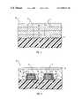
- FIG. 1is a partial cross-sectional elevation view of one embodiment of a multilayer structure prior to an etch, the multi-layer structure including a base silicon layer and a layer of undoped silicon dioxide, where the multi-layer structure has a layer of photoresist, and wherein a first selected pattern is defined in phantom.
- FIG. 2is a partial cross-sectional elevation view of the structure seen in FIG. 1 , wherein the layer of undoped silicon dioxide has been etched so as to form a recess terminating upon the base silicon layer, a layer of doped silicon dioxide has been deposited thereover, where a layer of photoresist is formed over the layer of doped silicon dioxide, and wherein a second selected pattern is defined in phantom which is intended to represent an etch through the layer of doped silicon dioxide to expose a contact on the base silicon layer that is self-aligned between the layer of undoped silicon dioxide, wherein the self-alignment of the etch is due to the selectivity of the etch to undoped silicon dioxide.
- FIG. 3is a partial cross-sectional elevation view of one embodiment of a multilayer structure prior to an etch, the multilayer structure including a base silicon layer and having thereon layers of gate oxide, polysilicon, tungsten silicide, and undoped silicon dioxide, where the multi-layer structure has a layer of photoresist, and wherein a first selected pattern is defined in phantom.
- FIG. 4is a partial cross-sectional elevation view of the structure seen in FIG. 3 , wherein gate stacks arc formed upon the base silicon layer, each gate stack having a spacer on a sidewall thereof and a cap on the top thereof, the gate stacks having deposited thereover a layer of doped silicon dioxide, and a layer of photoresist is deposited upon the layer of doped silicon dioxide, wherein a second selected pattern is defined in phantom which is intended to represent a fluorinated chemical etch through the layer of doped silicon dioxide to expose a contact on the base silicon layer that is self-aligned between the gate stacks, wherein the self-alignment of the etch is due to the selectivity of the etch to the materials of the spacers and the cap of the gate stacks.
- the inventive process hereinis directed towards selectively utilizing a plasma etch system on doped silicon dioxide (SiO 2 ) layer with a substantially undoped silicon dioxide layer as an etch stop.
- One application of the inventive processis to form a self-aligned contact.
- the present inventionalso discloses an inventive multilayer gate structure.
- a multilayer structure 10is created that comprises a base silicon layer 12 .
- a substantially undoped silicon dioxide layer 22Overlying silicon base layer 12 is a substantially undoped silicon dioxide layer 22 .
- Undoped silicon dioxide layer 22can be any type of undoped oxide and be formed by a thermal process, by a plasma enhanced deposition process, or by a conventional TEOS precursor deposition that is preferably rich in carbon or hydrogen, or by a precursor of gaseous silane (SiH 4 ) with oxygen. In the latter process, the gaseous silane flow will result in undoped silicon dioxide layer 22 .
- the next layer in the embodiment of multilayer structure 10 illustrated in FIG. 1comprises a photoresist layer 24 that is processed to expose a first selected pattern 15 , shown in phantom, such that silicon dioxide layer 22 will be used to create a topography in multilayer structure 10 .
- Multilayer structure 10is then anisotropically etched as shown by first selected pattern 15 to selectively remove material from undoped silicon dioxide layer 22 to form undoped silicon dioxide caps 16 as seen in FIG. 2 .
- a doped silicon dioxide layer 30is deposited over multilayer structure 10 as a passivation layer.
- doped silicon dioxide layer 30is substantially composed of borophosphosilicate glass (BPSG), borosilicate glass (BSG), or phosphosilicate glass (PSG).
- BPSGborophosphosilicate glass
- BSGborosilicate glass
- PSGphosphosilicate glass
- doped silicon dioxide layer 30is substantially composed of silicon dioxide having doping of about 3% or more for boron and about 3% or more for phosphorus.
- a photoresist layer 32is applied over doped silicon dioxide layer 30 . Photoresist layer 32 is processed to expose a second selected portion 17 of doped silicon dioxide layer 30 that is intended to be etched. Second selected portion 17 is seen in phantom in FIG. 2 .
- the structure seen in FIG. 2is now etched with a fluorinated or fluoro-carbon chemical etchant system to form second selected pattern 17 as illustrated in FIG. 2 .
- the preferred manneris an anisotropic plasma etch of doped silicon dioxide layer 30 down to the corresponding etch stop layer of undoped silicon dioxide cap 16 .
- the plasma etch technique employed hereinis preferably generated under a vacuum within the confines of a discharging unit and involves any type of a plasma system, including a high density plasma etcher.
- a conventional radio frequency reactive ion etcher (RF RIE) plasma system, a magnetically enhanced RIE (MERIE) plasma system, or an inductively coupled plasma systemcould be used.
- the preferred embodimentis an RF type RIE or MERIE plasma system.
- the plasma system being usedhas a plasma density in a range from about 10 9 /cm 3 to about 10 11 /cm 3
- a high density plasma systemcan also be used having a plasma density in a range from about 10 12 /cm 3 to about 10 13 /cm 3.
- FIG. 3One particular embodiment of a specific structure created utilizing the inventive process is illustrated in FIG. 3 wherein a multilayer structure 50 is created that comprises a base silicon layer 12 . Overlying silicon base layer 12 is a gate oxide layer 14 that covers silicon base layer 12 . Gate oxide layer 14 may be relatively thin in comparison with the other layers of the multilayered structure.
- the next layer in multilayer structure 50comprises a polysilicon gate layer 18 . Overlying polysilicon gate layer 18 is a refractory metal silicide layer 20 .
- a known benefit of refractory metal silicidesis their low resistivity.
- Refractory metal silicide layer 20may comprise any refractory metal including but not limited to titanium, tungsten, tantalum, and molybdenum.
- refractory metal silicide layer 20is substantially composed of tungsten silicide (WSi x ).
- Overlying refractory metal silicide layer 20is a substantially undoped silicon dioxide layer 22 which can be formed thermally, by plasma enhanced deposition, by a conventional TEOS precursor deposition that is preferably rich in carbon or hydrogen, or by a precursor of gascous silane (SiH 4 ) with oxygen.
- the next layer in multilayer structure 50is a photoresist layer 24 that is processed to expose a first selected pattern 15 shown in phantom. Multilayer structure 50 is then etched according to first selected pattern 15 to selectively remove material so as to form gate stacks 26 as illustrated in FIG. 4 . Each gate stack 26 has an undoped silicon dioxide cap 52 thereon which was formed from undoped silicon dioxide layer 22 .
- Spacer 28in on the sidewall of each gate stack 26 .
- Spacers 28are formed by subjecting a layer of silicon nitride deposited over gate stacks 26 to a spacer etch. Silicon nitride spacers 28 are generally perpendicular to silicon base layer 12 .
- spacers 28can be substantially composed of undoped silicon dioxide. As such, both spacers 28 and undoped silicon dioxide caps 52 can be made from the same materials and both act as an etch stop.
- a contact 34is defined therebetween upon silicon base layer 12 .
- a doped silicon dioxide layer 30composed of a material such as PSG, BSG, or BPSG, is deposited over multilayer structure 50 .
- a photoresist layer 32is then applied over doped silicon dioxide layer 30 .
- Photoresist layer 32is processed to create a second selected pattern 17 that is illustrated in phantom in FIG. 4 .
- the structure seen in FIG. 4is now etched with a fluorinated or fluoro-carbon chemical etchant system according to second selected pattern 17 .
- the preferred manner of etching of doped silicon dioxide layer 30 down to its corresponding etch stop layer, which is substantially undoped silicon dioxide layer 52is by a plasma etch.
- the etch technique employed hereinis preferably a plasma etch involving any type of a plasma system including a high density plasma etcher as previously discussed relative to FIG. 2 .
- the total pressurehas a preferred range from about 1 millitorr to about 400 millitorr.
- a more preferred pressure range for a plasma etchis in a pressure range from about 1 millitorr to about 100 millitorr.
- the most preferred pressure range for a plasma etchis from about 1 millitorr to about 75 millitorr.
- the pressuremay be increased, however, above the most preferred ranges.
- the RIE etchmay be performed at about 100 millitorr.
- Selectivitycan be optimized at a pressure range between about 10 millitorr and about 75 millitorr. Pressure increases may result in a loss in selectivity.
- the range in selectivitycan be adjusted to accommodate different pressures. As such, selectivity and pressure are inversely related.
- a preferable temperature range during the plasma etchhas a range of about 10° C. to about 80° C., and more preferably about 20° C. to about 40° C. This is the temperature of a bottom electrode adjacent to silicon layer 12 during the etching process.
- the preferable range of the semiconductor materialsis between about 40° C. and about 130° C., and more preferably between about 40° C. and about 90° C.
- Undoped silicon dioxide cap 52 and silicon nitride spacers 28protect gate stacks 26 from the fluorinated chemical etch. As illustrated in FIG. 4 , the etch will selectively and anisotropically remove doped silicon dioxide layer 30 above contact 34 as indicated by second selected pattern 17 . The etch removes material from doped silicon dioxide layer 30 at a higher material removal rate than that of undoped silicon dioxide cap 52 and silicon nitride spacers or undoped silicon dioxide spacers 28 . Preferably, the etch has a material removal rate for doped silicon dioxide is at least 10 times higher than that of undoped silicon dioxide. As such contact 34 is self-aligned between spacers 28 of gate stacks 26 .
- the self-aligning aspect of contact 34is due to the selectivity of the etch which assures that even in cases of misalignment of the exposure of second selected pattern 17 , the fluorinated chemical etch through doped silicon dioxide layer 30 will properly place contact 34 on silicon base layer 12 and between adjacent silicon nitride spacers 28 that have been formed upon sides of gate stacks 26 .
- Contact 34is preferably exposed by an anisotropic plasma etch with a fluorinated chemistry that etches through BSG, PSG, BPSG, or doped silicon dioxide in general.
- the etchis preferably selective to undoped silicon dioxide, silicon, and silicon nitride.
- the fluorinated chemical etchutilizes a type of carbon fluorine gas from the group consisting of C 2 F 6 , CF 4 , C 3 F 8 , C 4 F 10 , C 2 F 8 , CH 2 F 2 , CHF 3 , C 2 HF 5 , CH 3 F and combinations thereof.
- fluorinated enchantsin a substantially gas phase during the etching of the structure.
- an inert gasis often used in combination with the fluorinated etchant.
- Argon, nitrogen, and heliumare examples of such an inert gas.
- the preferred gassesare CF 4 , CH 2 F 2 , CHF 3 and Ar.
- CH 3 Fmay be used in place of CH 2 F 2 .
- the preferred enchantis a fluorine deficient gas which is defined as a gas where there are not enough fluorine atoms to saturate the bonding for the carbon atoms.
- a conductive materialis formed upon contact 34 between spacers 28 within second selected pattern 17 as shown in FIG. 4 .
- the conductive materialwill form a contact plug to contact 34 . It may be desirable to clad the contact plug with a refractory metal or a refractory metal silicide. As such, second selected pattern 17 would have proximate thereto the refractory metal or silicide thereof prior to formation of the contact plug in contact with contact 34 .
- the present inventionhas application to a wide variety of structures.
- the top layer of the gate stackcomposed of undoped silicon dioxide, can be used to create and protect various types of structures during the doped silicon dioxide etching process for structures other than gate stacks.
- the present inventionallows the gate stack height to be reduced.
- One advantage of reducing the gate stack heightis to reduce the process time which results in greater throughput.
- the reduced gate heightresults in a lower etch time and a reduced contact hole aspect ratio, the latter being defined as the ratio of height to width of the contact hole.
- By reducing the aspect ratio, or by reducing the height of the gate stackthere will be a decrease in the etch time.
- Another advantage of a lower gate stack heightis that it reduces the overall topography which in turn results in it being easier to planarize and to use photolithographic processes. As such, the present invention increases yield.
Landscapes
- Engineering & Computer Science (AREA)
- Manufacturing & Machinery (AREA)
- Power Engineering (AREA)
- General Physics & Mathematics (AREA)
- Physics & Mathematics (AREA)
- Computer Hardware Design (AREA)
- Condensed Matter Physics & Semiconductors (AREA)
- Microelectronics & Electronic Packaging (AREA)
- Chemical & Material Sciences (AREA)
- General Chemical & Material Sciences (AREA)
- Chemical Kinetics & Catalysis (AREA)
- Inorganic Chemistry (AREA)
- Drying Of Semiconductors (AREA)
- Internal Circuitry In Semiconductor Integrated Circuit Devices (AREA)
- Insulated Gate Type Field-Effect Transistor (AREA)
- Electrodes Of Semiconductors (AREA)
- Semiconductor Memories (AREA)
Abstract
Description
Claims (98)
Priority Applications (10)
| Application Number | Priority Date | Filing Date | Title |
|---|---|---|---|
| US08/846,671US6849557B1 (en) | 1997-04-30 | 1997-04-30 | Undoped silicon dioxide as etch stop for selective etch of doped silicon dioxide |
| US08/958,290US6551940B1 (en) | 1997-04-30 | 1997-10-27 | Undoped silicon dioxide as etch mask for patterning of doped silicon dioxide |
| PCT/US1998/002826WO1998049719A1 (en) | 1997-04-30 | 1998-02-16 | Undoped silicon dioxide as etch stop for selective etch of doped silicon dioxide |
| AU61646/98AAU6164698A (en) | 1997-04-30 | 1998-02-16 | Undoped silicon dioxide as etch stop for selective etch of doped silicon dioxide |
| JP54694798AJP2001522531A (en) | 1997-04-30 | 1998-02-16 | Method for selectively plasma etching structures on a semiconductor substrate |
| TW087102108ATW507293B (en) | 1997-04-30 | 1998-02-16 | Undoped silicon dioxide as etch stop for selective etch of doped silicon dioxide |
| KR10-1999-7009177AKR100489978B1 (en) | 1997-04-30 | 1998-02-16 | Undoped silicon dioxide as etch stop for selective etch of doped silicon dioxide |
| EP98906417AEP1004139A4 (en) | 1997-04-30 | 1998-02-16 | NON-DOPED SILICON DIOXIDE AS AN ATTACK STOP FOR SELECTIVE ATTACK OF DOPED SILICON DIOXIDE |
| US09/577,390US6479864B1 (en) | 1997-04-30 | 2000-05-25 | Semiconductor structure having a plurality of gate stacks |
| US09/579,402US6967408B1 (en) | 1997-04-30 | 2000-05-25 | Gate stack structure |
Applications Claiming Priority (1)
| Application Number | Priority Date | Filing Date | Title |
|---|---|---|---|
| US08/846,671US6849557B1 (en) | 1997-04-30 | 1997-04-30 | Undoped silicon dioxide as etch stop for selective etch of doped silicon dioxide |
Related Child Applications (2)
| Application Number | Title | Priority Date | Filing Date |
|---|---|---|---|
| US08/958,290Continuation-In-PartUS6551940B1 (en) | 1997-04-30 | 1997-10-27 | Undoped silicon dioxide as etch mask for patterning of doped silicon dioxide |
| US09/579,402DivisionUS6967408B1 (en) | 1997-04-30 | 2000-05-25 | Gate stack structure |
Publications (1)
| Publication Number | Publication Date |
|---|---|
| US6849557B1true US6849557B1 (en) | 2005-02-01 |
Family
ID=25298608
Family Applications (4)
| Application Number | Title | Priority Date | Filing Date |
|---|---|---|---|
| US08/846,671Expired - Fee RelatedUS6849557B1 (en) | 1997-04-30 | 1997-04-30 | Undoped silicon dioxide as etch stop for selective etch of doped silicon dioxide |
| US08/958,290Expired - LifetimeUS6551940B1 (en) | 1997-04-30 | 1997-10-27 | Undoped silicon dioxide as etch mask for patterning of doped silicon dioxide |
| US09/579,402Expired - Fee RelatedUS6967408B1 (en) | 1997-04-30 | 2000-05-25 | Gate stack structure |
| US09/577,390Expired - LifetimeUS6479864B1 (en) | 1997-04-30 | 2000-05-25 | Semiconductor structure having a plurality of gate stacks |
Family Applications After (3)
| Application Number | Title | Priority Date | Filing Date |
|---|---|---|---|
| US08/958,290Expired - LifetimeUS6551940B1 (en) | 1997-04-30 | 1997-10-27 | Undoped silicon dioxide as etch mask for patterning of doped silicon dioxide |
| US09/579,402Expired - Fee RelatedUS6967408B1 (en) | 1997-04-30 | 2000-05-25 | Gate stack structure |
| US09/577,390Expired - LifetimeUS6479864B1 (en) | 1997-04-30 | 2000-05-25 | Semiconductor structure having a plurality of gate stacks |
Country Status (7)
| Country | Link |
|---|---|
| US (4) | US6849557B1 (en) |
| EP (1) | EP1004139A4 (en) |
| JP (1) | JP2001522531A (en) |
| KR (1) | KR100489978B1 (en) |
| AU (1) | AU6164698A (en) |
| TW (1) | TW507293B (en) |
| WO (1) | WO1998049719A1 (en) |
Cited By (13)
| Publication number | Priority date | Publication date | Assignee | Title |
|---|---|---|---|---|
| US20030178389A1 (en)* | 2001-07-09 | 2003-09-25 | Mitsuhiro Yuasa | Method of forming via metal layers and via metal layer-formed substrate |
| US20040248413A1 (en)* | 2000-04-27 | 2004-12-09 | Micron Technology, Inc. | Etchant and method of use |
| US20050023242A1 (en)* | 2003-06-27 | 2005-02-03 | Lam Research Corporation | Method for bilayer resist plasma etch |
| US20050098536A1 (en)* | 2003-11-12 | 2005-05-12 | Applied Materials, Inc. | Method of etching oxide with high selectivity |
| US20050211672A1 (en)* | 2001-08-30 | 2005-09-29 | Kei-Yu Ko | Etch-processing apparatus |
| US20060097327A1 (en)* | 1998-09-03 | 2006-05-11 | Hermes Michael J | Low resistance semiconductor process and structures |
| US20060183308A1 (en)* | 2003-12-10 | 2006-08-17 | Ying Zhang | Method of etching dual pre-doped polysilicon gate stacks using carbon-containing gases additions |
| US20100055921A1 (en)* | 2008-08-29 | 2010-03-04 | Air Products And Chemicals, Inc. | Selective Etching of Silicon Dioxide Compositions |
| US20120061837A1 (en)* | 2010-09-15 | 2012-03-15 | Kabushiki Kaisha Toshiba | Method of manufacturing semiconductor device and semiconductor device |
| US9419109B2 (en)* | 2014-10-24 | 2016-08-16 | United Microelectronics Corp. | Semiconductor device and method for fabricating the same |
| US12369501B2 (en) | 2012-03-08 | 2025-07-22 | 1372934 B.C. Ltd. | Systems and methods for fabrication of superconducting integrated circuits |
| US12376501B2 (en) | 2020-05-11 | 2025-07-29 | 1372934 B.C. Ltd. | Kinetic inductance devices, methods for fabricating kinetic inductance devices, and articles employing the same |
| US12392823B2 (en) | 2021-11-05 | 2025-08-19 | D-Wave Systems Inc. | Systems and methods for on-chip noise measurements |
Families Citing this family (22)
| Publication number | Priority date | Publication date | Assignee | Title |
|---|---|---|---|---|
| US6849557B1 (en) | 1997-04-30 | 2005-02-01 | Micron Technology, Inc. | Undoped silicon dioxide as etch stop for selective etch of doped silicon dioxide |
| US6117791A (en) | 1998-06-22 | 2000-09-12 | Micron Technology, Inc. | Etchant with selectivity for doped silicon dioxide over undoped silicon dioxide and silicon nitride, processes which employ the etchant, and structures formed thereby |
| US7173339B1 (en) | 1998-06-22 | 2007-02-06 | Micron Technology, Inc. | Semiconductor device having a substrate an undoped silicon oxide structure and an overlaying doped silicon oxide structure with a sidewall terminating at the undoped silicon oxide structure |
| US6875371B1 (en) | 1998-06-22 | 2005-04-05 | Micron Technology, Inc. | Etchant with selectivity for doped silicon dioxide over undoped silicon dioxide and silicon nitride, processes which employ the etchant, and structures formed thereby |
| US6432833B1 (en) | 1999-12-20 | 2002-08-13 | Micron Technology, Inc. | Method of forming a self aligned contact opening |
| WO2001050518A1 (en)* | 2000-01-03 | 2001-07-12 | Micron Technology, Inc. | Method of forming a self-aligned contact opening |
| US6638843B1 (en)* | 2000-03-23 | 2003-10-28 | Micron Technology, Inc. | Method for forming a silicide gate stack for use in a self-aligned contact etch |
| EP1297564B1 (en)* | 2000-07-05 | 2008-09-17 | Micron Technology, Inc. | Process for selectively etching doped silicon dioxide over undoped silicon dioxide |
| US6503841B1 (en) | 2000-07-07 | 2003-01-07 | Agere Systems Inc. | Oxide etch |
| US6740601B2 (en)* | 2001-05-11 | 2004-05-25 | Applied Materials Inc. | HDP-CVD deposition process for filling high aspect ratio gaps |
| KR100726145B1 (en)* | 2002-07-19 | 2007-06-13 | 주식회사 하이닉스반도체 | Semiconductor device manufacturing method |
| US6806535B2 (en)* | 2003-01-22 | 2004-10-19 | Macronix International Co., Ltd. | Non-volatile memory and fabricating method thereof |
| US6903031B2 (en)* | 2003-09-03 | 2005-06-07 | Applied Materials, Inc. | In-situ-etch-assisted HDP deposition using SiF4 and hydrogen |
| KR100563487B1 (en)* | 2003-12-31 | 2006-03-27 | 동부아남반도체 주식회사 | Metal wiring formation method of semiconductor device |
| US7858481B2 (en)* | 2005-06-15 | 2010-12-28 | Intel Corporation | Method for fabricating transistor with thinned channel |
| WO2008086228A2 (en) | 2007-01-04 | 2008-07-17 | University Of Washington | Arrays and methods for guided cell patterning |
| US8232607B2 (en) | 2010-11-23 | 2012-07-31 | International Business Machines Corporation | Borderless contact for replacement gate employing selective deposition |
| US8735299B2 (en)* | 2011-03-03 | 2014-05-27 | Tokyo Electron Limited | Semiconductor device manufacturing method and computer-readable storage medium |
| US8748252B1 (en) | 2012-11-26 | 2014-06-10 | International Business Machines Corporation | Replacement metal gate transistors using bi-layer hardmask |
| US9018108B2 (en) | 2013-01-25 | 2015-04-28 | Applied Materials, Inc. | Low shrinkage dielectric films |
| US9318574B2 (en) | 2014-06-18 | 2016-04-19 | International Business Machines Corporation | Method and structure for enabling high aspect ratio sacrificial gates |
| US9570450B1 (en) | 2015-11-19 | 2017-02-14 | International Business Machines Corporation | Hybrid logic and SRAM contacts |
Citations (44)
| Publication number | Priority date | Publication date | Assignee | Title |
|---|---|---|---|---|
| JPS56114355A (en)* | 1980-02-14 | 1981-09-08 | Chiyou Lsi Gijutsu Kenkyu Kumiai | Manufacture of semiconductor device |
| US4381201A (en) | 1980-03-11 | 1983-04-26 | Fujitsu Limited | Method for production of semiconductor devices |
| US4472729A (en) | 1981-08-31 | 1984-09-18 | Tokyo Shibaura Denki Kabushiki Kaisha | Recrystallized three dimensional integrated circuit |
| US4489478A (en) | 1981-09-29 | 1984-12-25 | Fujitsu Limited | Process for producing a three-dimensional semiconductor device |
| JPS61133666A (en) | 1984-12-03 | 1986-06-20 | Nec Corp | Manufacturing method of semiconductor device |
| US4681657A (en) | 1985-10-31 | 1987-07-21 | International Business Machines Corporation | Preferential chemical etch for doped silicon |
| EP0265584A2 (en) | 1986-10-30 | 1988-05-04 | International Business Machines Corporation | Method and materials for etching silicon dioxide using silicon nitride or silicon rich dioxide as an etch barrier |
| US4753709A (en) | 1987-02-05 | 1988-06-28 | Texas Instuments Incorporated | Method for etching contact vias in a semiconductor device |
| US4966865A (en) | 1987-02-05 | 1990-10-30 | Texas Instruments Incorporated | Method for planarization of a semiconductor device prior to metallization |
| US5022958A (en)* | 1990-06-27 | 1991-06-11 | At&T Bell Laboratories | Method of etching for integrated circuits with planarized dielectric |
| US5084417A (en) | 1989-01-06 | 1992-01-28 | International Business Machines Corporation | Method for selective deposition of refractory metals on silicon substrates and device formed thereby |
| US5150276A (en) | 1992-01-24 | 1992-09-22 | Micron Technology, Inc. | Method of fabricating a vertical parallel cell capacitor having a storage node capacitor plate comprising a center fin effecting electrical communication between itself and parallel annular rings |
| JPH04345054A (en) | 1991-05-22 | 1992-12-01 | Ricoh Co Ltd | Semiconductor device and its manufacture |
| JPH04360570A (en) | 1991-06-06 | 1992-12-14 | Mitsubishi Electric Corp | Stacked semiconductor device |
| US5252517A (en) | 1992-12-10 | 1993-10-12 | Micron Semiconductor, Inc. | Method of conductor isolation from a conductive contact plug |
| JPH05335482A (en) | 1992-05-29 | 1993-12-17 | Semiconductor Energy Lab Co Ltd | Multilayer semiconductor integrated circuit having thin film transistor |
| US5286344A (en) | 1992-06-15 | 1994-02-15 | Micron Technology, Inc. | Process for selectively etching a layer of silicon dioxide on an underlying stop layer of silicon nitride |
| US5321286A (en) | 1991-11-26 | 1994-06-14 | Nec Corporation | Non-volatile semiconductor memory device having thin film memory transistors stacked over associated selecting transistors |
| US5362666A (en) | 1992-09-18 | 1994-11-08 | Micron Technology, Inc. | Method of producing a self-aligned contact penetrating cell plate |
| US5366590A (en) | 1993-03-19 | 1994-11-22 | Sony Corporation | Dry etching method |
| US5374332A (en) | 1991-02-20 | 1994-12-20 | Canon Kabushiki Kaisha | Method for etching silicon compound film and process for forming article by utilizing the method |
| US5401681A (en) | 1993-02-12 | 1995-03-28 | Micron Technology, Inc. | Method of forming a bit line over capacitor array of memory cells |
| US5423945A (en) | 1992-09-08 | 1995-06-13 | Applied Materials, Inc. | Selectivity for etching an oxide over a nitride |
| US5429070A (en) | 1989-06-13 | 1995-07-04 | Plasma & Materials Technologies, Inc. | High density plasma deposition and etching apparatus |
| US5445712A (en) | 1992-03-25 | 1995-08-29 | Sony Corporation | Dry etching method |
| US5626716A (en) | 1995-09-29 | 1997-05-06 | Lam Research Corporation | Plasma etching of semiconductors |
| US5643819A (en) | 1995-10-30 | 1997-07-01 | Vanguard International Semiconductor Corporation | Method of fabricating fork-shaped stacked capacitors for DRAM cells |
| US5677227A (en) | 1996-09-09 | 1997-10-14 | Vanguard International Semiconductor Corporation | Method of fabricating single crown, extendible to triple crown, stacked capacitor structures, using a self-aligned capacitor node contact |
| US5685951A (en) | 1996-02-15 | 1997-11-11 | Micron Technology, Inc. | Methods and etchants for etching oxides of silicon with low selectivity in a vapor phase system |
| US5700731A (en) | 1995-12-07 | 1997-12-23 | Vanguard International Semiconductor Corporation | Method for manufacturing crown-shaped storage capacitors on dynamic random access memory cells |
| US5712202A (en) | 1995-12-27 | 1998-01-27 | Vanguard International Semiconductor Corporation | Method for fabricating a multiple walled crown capacitor of a semiconductor device |
| US5731130A (en) | 1996-11-12 | 1998-03-24 | Vanguard International Semiconductor Corporation | Method for fabricating stacked capacitors on dynamic random access memory cells |
| US5736455A (en) | 1995-12-22 | 1998-04-07 | Micron Technology, Inc. | Method for passivating the sidewalls of a tungsten word line |
| US5792689A (en) | 1997-04-11 | 1998-08-11 | Vanguard International Semiconducter Corporation | Method for manufacturing double-crown capacitors self-aligned to node contacts on dynamic random access memory |
| US5828096A (en) | 1996-03-29 | 1998-10-27 | Mitsubishi Denki Kabushiki Kaisha | Semiconductor device having a contact hole |
| US5883436A (en)* | 1994-11-18 | 1999-03-16 | Intel Corporation | Contact and via fabrication technologies |
| US5897352A (en) | 1998-03-25 | 1999-04-27 | Vanguard International Semiconductor Corporation | Method of manufacturing hemispherical grained polysilicon with improved adhesion and reduced capacitance depletion |
| US5918120A (en) | 1998-07-24 | 1999-06-29 | Taiwan Semiconductor Manufacturing Company, Ltd. | Method for fabricating capacitor-over-bit line (COB) dynamic random access memory (DRAM) using tungsten landing plug contacts and Ti/TiN bit lines |
| US5936272A (en) | 1995-06-23 | 1999-08-10 | Samsung Electronics Co., Ltd. | DRAM transistor cells with a self-aligned storage electrode contact |
| US5986299A (en) | 1996-11-05 | 1999-11-16 | Hitachi, Ltd. | Semiconductor integrated circuit device having multi-level wiring capacitor structures |
| US5990507A (en) | 1996-07-09 | 1999-11-23 | Kabushiki Kaisha Toshiba | Semiconductor device having ferroelectric capacitor structures |
| US6124191A (en) | 1997-12-31 | 2000-09-26 | Intel Corporation | Self-aligned contact process using low density/low k dielectric |
| US6242759B1 (en) | 1991-03-27 | 2001-06-05 | Semiconductor Energy Laboratory Co., Ltd. | Semiconductor device and method for forming the same |
| US6271542B1 (en) | 1997-12-08 | 2001-08-07 | International Business Machines Corporation | Merged logic and memory combining thin film and bulk Si transistors |
Family Cites Families (67)
| Publication number | Priority date | Publication date | Assignee | Title |
|---|---|---|---|---|
| JPS6042821A (en) | 1983-08-17 | 1985-03-07 | Mitsubishi Electric Corp | Manufacture of semiconductor device |
| JPS6063926A (en)* | 1983-08-31 | 1985-04-12 | Fujitsu Ltd | Manufacture of semiconductor device |
| DE3443453A1 (en) | 1984-11-29 | 1986-05-28 | Varta Batterie Ag, 3000 Hannover | EXPLOSION-PROOF, SEALED GALVANIC ELEMENT |
| US4807016A (en) | 1985-07-15 | 1989-02-21 | Texas Instruments Incorporated | Dry etch of phosphosilicate glass with selectivity to undoped oxide |
| US4818335A (en)* | 1988-05-13 | 1989-04-04 | The United States Of America As Represented By The Director Of The National Security Agency | Tapered wet etching of contacts using a trilayer silox structure |
| US5229311A (en)* | 1989-03-22 | 1993-07-20 | Intel Corporation | Method of reducing hot-electron degradation in semiconductor devices |
| GB8907898D0 (en) | 1989-04-07 | 1989-05-24 | Inmos Ltd | Semiconductor devices and fabrication thereof |
| GB2233820A (en) | 1989-06-26 | 1991-01-16 | Philips Nv | Providing an electrode on a semiconductor device |
| US5208176A (en) | 1990-01-16 | 1993-05-04 | Micron Technology, Inc. | Method of fabricating an enhanced dynamic random access memory (DRAM) cell capacitor using multiple polysilicon texturization |
| JPH046146A (en) | 1990-04-24 | 1992-01-10 | Hitachi Chem Co Ltd | High temperature superconductor and production thereof |
| US5037777A (en) | 1990-07-02 | 1991-08-06 | Motorola Inc. | Method for forming a multi-layer semiconductor device using selective planarization |
| US5298465A (en) | 1990-08-16 | 1994-03-29 | Applied Materials, Inc. | Plasma etching system |
| JPH04239723A (en) | 1991-01-23 | 1992-08-27 | Nec Corp | Manufacture of semiconductor device |
| US5269879A (en) | 1991-10-16 | 1993-12-14 | Lam Research Corporation | Method of etching vias without sputtering of underlying electrically conductive layer |
| US5658425A (en) | 1991-10-16 | 1997-08-19 | Lam Research Corporation | Method of etching contact openings with reduced removal rate of underlying electrically conductive titanium silicide layer |
| US5192703A (en) | 1991-10-31 | 1993-03-09 | Micron Technology, Inc. | Method of making tungsten contact core stack capacitor |
| US5210047A (en) | 1991-12-12 | 1993-05-11 | Woo Been Jon K | Process for fabricating a flash EPROM having reduced cell size |
| US5323047A (en)* | 1992-01-31 | 1994-06-21 | Sgs-Thomson Microelectronics, Inc. | Structure formed by a method of patterning a submicron semiconductor layer |
| US5300813A (en)* | 1992-02-26 | 1994-04-05 | International Business Machines Corporation | Refractory metal capped low resistivity metal conductor lines and vias |
| DE69318880T2 (en)* | 1992-03-31 | 1998-10-08 | Sgs Thomson Microelectronics | Planarization process from an integrated circuit |
| JP3097338B2 (en) | 1992-08-14 | 2000-10-10 | 松下電器産業株式会社 | Method of forming contact hole |
| US5312768A (en) | 1993-03-09 | 1994-05-17 | Micron Technology, Inc. | Integrated process for fabricating raised, source/drain, short-channel transistors |
| US5478772A (en) | 1993-04-02 | 1995-12-26 | Micron Technology, Inc. | Method for forming a storage cell capacitor compatible with high dielectric constant materials |
| FR2711275B1 (en) | 1993-10-15 | 1996-10-31 | Intel Corp | Automatically aligned contact process in semiconductor and product device manufacturing. |
| US5393704A (en)* | 1993-12-13 | 1995-02-28 | United Microelectronics Corporation | Self-aligned trenched contact (satc) process |
| JPH07263415A (en) | 1994-03-18 | 1995-10-13 | Fujitsu Ltd | Method for manufacturing semiconductor device |
| US5685914A (en) | 1994-04-05 | 1997-11-11 | Applied Materials, Inc. | Focus ring for semiconductor wafer processing in a plasma reactor |
| US5565384A (en) | 1994-04-28 | 1996-10-15 | Texas Instruments Inc | Self-aligned via using low permittivity dielectric |
| US5430328A (en)* | 1994-05-31 | 1995-07-04 | United Microelectronics Corporation | Process for self-align contact |
| JPH07335612A (en) | 1994-06-13 | 1995-12-22 | Hitachi Ltd | Method for manufacturing semiconductor integrated circuit device |
| US5504041A (en) | 1994-08-01 | 1996-04-02 | Texas Instruments Incorporated | Conductive exotic-nitride barrier layer for high-dielectric-constant materials |
| US5482894A (en) | 1994-08-23 | 1996-01-09 | Texas Instruments Incorporated | Method of fabricating a self-aligned contact using organic dielectric materials |
| KR0161731B1 (en) | 1994-10-28 | 1999-02-01 | 김주용 | Microcontact Formation Method of Semiconductor Device |
| US5705427A (en)* | 1994-12-22 | 1998-01-06 | Sgs-Thomson Microelectronics, Inc. | Method of forming a landing pad structure in an integrated circuit |
| JPH08181121A (en) | 1994-12-27 | 1996-07-12 | Sony Corp | Manufacture of semiconductor device |
| JPH08250449A (en) | 1995-03-09 | 1996-09-27 | Sony Corp | Formation of connecting hole for semiconductor device |
| JP3351183B2 (en) | 1995-06-19 | 2002-11-25 | 株式会社デンソー | Dry etching method and trench forming method for silicon substrate |
| US5935877A (en) | 1995-09-01 | 1999-08-10 | Applied Materials, Inc. | Etch process for forming contacts over titanium silicide |
| US5792703A (en) | 1996-03-20 | 1998-08-11 | International Business Machines Corporation | Self-aligned contact wiring process for SI devices |
| US5783496A (en) | 1996-03-29 | 1998-07-21 | Lam Research Corporation | Methods and apparatus for etching self-aligned contacts |
| US5946568A (en) | 1996-05-17 | 1999-08-31 | Mosel Vitelic, Inc. | Self aligned method of fabricating a DRAM with improved capacitance |
| US5908320A (en) | 1996-06-26 | 1999-06-01 | Lam Research Corporation | High selectivity BPSG:TiSi2 contact etch process |
| US6362527B1 (en)* | 1996-11-21 | 2002-03-26 | Advanced Micro Devices, Inc. | Borderless vias on bottom metal |
| US5747369A (en) | 1997-01-13 | 1998-05-05 | Chartered Semiconductor Manufacturing Ltd. | Formation of a capacitor using a sacrificial etch stop |
| US5821594A (en) | 1997-02-25 | 1998-10-13 | Nec Corporation | Semiconductor device having a self-aligned type contact hole |
| US6065481A (en) | 1997-03-26 | 2000-05-23 | Fsi International, Inc. | Direct vapor delivery of enabling chemical for enhanced HF etch process performance |
| US5831899A (en)* | 1997-04-07 | 1998-11-03 | Integrated Device Technology, Inc. | Local interconnect structure and process for six-transistor SRAM cell |
| US5817579A (en) | 1997-04-09 | 1998-10-06 | Vanguard International Semiconductor Corporation | Two step plasma etch method for forming self aligned contact |
| US5780338A (en) | 1997-04-11 | 1998-07-14 | Vanguard International Semiconductor Corporation | Method for manufacturing crown-shaped capacitors for dynamic random access memory integrated circuits |
| US6849557B1 (en) | 1997-04-30 | 2005-02-01 | Micron Technology, Inc. | Undoped silicon dioxide as etch stop for selective etch of doped silicon dioxide |
| US6153490A (en) | 1997-07-01 | 2000-11-28 | Texas Instruments Incorporated | Method for forming integrated circuit capacitor and memory |
| US5920796A (en)* | 1997-09-05 | 1999-07-06 | Advanced Micro Devices, Inc. | In-situ etch of BARC layer during formation of local interconnects |
| US6074488A (en) | 1997-09-16 | 2000-06-13 | Applied Materials, Inc | Plasma chamber support having an electrically coupled collar ring |
| US6183655B1 (en) | 1997-09-19 | 2001-02-06 | Applied Materials, Inc. | Tunable process for selectively etching oxide using fluoropropylene and a hydrofluorocarbon |
| US6159862A (en) | 1997-12-27 | 2000-12-12 | Tokyo Electron Ltd. | Semiconductor processing method and system using C5 F8 |
| US6171970B1 (en) | 1998-01-27 | 2001-01-09 | Texas Instruments Incorporated | Method for forming high-density integrated circuit capacitors |
| US6174451B1 (en) | 1998-03-27 | 2001-01-16 | Applied Materials, Inc. | Oxide etch process using hexafluorobutadiene and related unsaturated hydrofluorocarbons |
| US6165880A (en) | 1998-06-15 | 2000-12-26 | Taiwan Semiconductor Manufacturing Company | Double spacer technology for making self-aligned contacts (SAC) on semiconductor integrated circuits |
| US6117791A (en) | 1998-06-22 | 2000-09-12 | Micron Technology, Inc. | Etchant with selectivity for doped silicon dioxide over undoped silicon dioxide and silicon nitride, processes which employ the etchant, and structures formed thereby |
| US6277758B1 (en) | 1998-07-23 | 2001-08-21 | Micron Technology, Inc. | Method of etching doped silicon dioxide with selectivity to undoped silicon dioxide with a high density plasma etcher |
| US6254966B1 (en) | 1998-08-04 | 2001-07-03 | Victor Company Of Japan, Ltd. | Information recording mediums, supporter used in the mediums, manufacture methods of the supporter, manufacturing apparatus of the supporter and stampers for producing the mediums |
| US6117788A (en) | 1998-09-01 | 2000-09-12 | Micron Technology, Inc. | Semiconductor etching methods |
| US6432833B1 (en) | 1999-12-20 | 2002-08-13 | Micron Technology, Inc. | Method of forming a self aligned contact opening |
| WO2001050518A1 (en) | 2000-01-03 | 2001-07-12 | Micron Technology, Inc. | Method of forming a self-aligned contact opening |
| US6337285B1 (en) | 2000-03-21 | 2002-01-08 | Micron Technology, Inc. | Self-aligned contact (SAC) etch with dual-chemistry process |
| US6362109B1 (en) | 2000-06-02 | 2002-03-26 | Applied Materials, Inc. | Oxide/nitride etching having high selectivity to photoresist |
| US6372605B1 (en) | 2000-06-26 | 2002-04-16 | Agere Systems Guardian Corp. | Additional etching to decrease polishing time for shallow-trench isolation in semiconductor processing |
- 1997
- 1997-04-30USUS08/846,671patent/US6849557B1/ennot_activeExpired - Fee Related
- 1997-10-27USUS08/958,290patent/US6551940B1/ennot_activeExpired - Lifetime
- 1998
- 1998-02-16TWTW087102108Apatent/TW507293B/ennot_activeIP Right Cessation
- 1998-02-16AUAU61646/98Apatent/AU6164698A/ennot_activeAbandoned
- 1998-02-16KRKR10-1999-7009177Apatent/KR100489978B1/ennot_activeExpired - Lifetime
- 1998-02-16EPEP98906417Apatent/EP1004139A4/ennot_activeCeased
- 1998-02-16JPJP54694798Apatent/JP2001522531A/enactivePending
- 1998-02-16WOPCT/US1998/002826patent/WO1998049719A1/enactiveIP Right Grant
- 2000
- 2000-05-25USUS09/579,402patent/US6967408B1/ennot_activeExpired - Fee Related
- 2000-05-25USUS09/577,390patent/US6479864B1/ennot_activeExpired - Lifetime
Patent Citations (44)
| Publication number | Priority date | Publication date | Assignee | Title |
|---|---|---|---|---|
| JPS56114355A (en)* | 1980-02-14 | 1981-09-08 | Chiyou Lsi Gijutsu Kenkyu Kumiai | Manufacture of semiconductor device |
| US4381201A (en) | 1980-03-11 | 1983-04-26 | Fujitsu Limited | Method for production of semiconductor devices |
| US4472729A (en) | 1981-08-31 | 1984-09-18 | Tokyo Shibaura Denki Kabushiki Kaisha | Recrystallized three dimensional integrated circuit |
| US4489478A (en) | 1981-09-29 | 1984-12-25 | Fujitsu Limited | Process for producing a three-dimensional semiconductor device |
| JPS61133666A (en) | 1984-12-03 | 1986-06-20 | Nec Corp | Manufacturing method of semiconductor device |
| US4681657A (en) | 1985-10-31 | 1987-07-21 | International Business Machines Corporation | Preferential chemical etch for doped silicon |
| EP0265584A2 (en) | 1986-10-30 | 1988-05-04 | International Business Machines Corporation | Method and materials for etching silicon dioxide using silicon nitride or silicon rich dioxide as an etch barrier |
| US4753709A (en) | 1987-02-05 | 1988-06-28 | Texas Instuments Incorporated | Method for etching contact vias in a semiconductor device |
| US4966865A (en) | 1987-02-05 | 1990-10-30 | Texas Instruments Incorporated | Method for planarization of a semiconductor device prior to metallization |
| US5084417A (en) | 1989-01-06 | 1992-01-28 | International Business Machines Corporation | Method for selective deposition of refractory metals on silicon substrates and device formed thereby |
| US5429070A (en) | 1989-06-13 | 1995-07-04 | Plasma & Materials Technologies, Inc. | High density plasma deposition and etching apparatus |
| US5022958A (en)* | 1990-06-27 | 1991-06-11 | At&T Bell Laboratories | Method of etching for integrated circuits with planarized dielectric |
| US5374332A (en) | 1991-02-20 | 1994-12-20 | Canon Kabushiki Kaisha | Method for etching silicon compound film and process for forming article by utilizing the method |
| US6242759B1 (en) | 1991-03-27 | 2001-06-05 | Semiconductor Energy Laboratory Co., Ltd. | Semiconductor device and method for forming the same |
| JPH04345054A (en) | 1991-05-22 | 1992-12-01 | Ricoh Co Ltd | Semiconductor device and its manufacture |
| JPH04360570A (en) | 1991-06-06 | 1992-12-14 | Mitsubishi Electric Corp | Stacked semiconductor device |
| US5321286A (en) | 1991-11-26 | 1994-06-14 | Nec Corporation | Non-volatile semiconductor memory device having thin film memory transistors stacked over associated selecting transistors |
| US5150276A (en) | 1992-01-24 | 1992-09-22 | Micron Technology, Inc. | Method of fabricating a vertical parallel cell capacitor having a storage node capacitor plate comprising a center fin effecting electrical communication between itself and parallel annular rings |
| US5445712A (en) | 1992-03-25 | 1995-08-29 | Sony Corporation | Dry etching method |
| JPH05335482A (en) | 1992-05-29 | 1993-12-17 | Semiconductor Energy Lab Co Ltd | Multilayer semiconductor integrated circuit having thin film transistor |
| US5286344A (en) | 1992-06-15 | 1994-02-15 | Micron Technology, Inc. | Process for selectively etching a layer of silicon dioxide on an underlying stop layer of silicon nitride |
| US5423945A (en) | 1992-09-08 | 1995-06-13 | Applied Materials, Inc. | Selectivity for etching an oxide over a nitride |
| US5362666A (en) | 1992-09-18 | 1994-11-08 | Micron Technology, Inc. | Method of producing a self-aligned contact penetrating cell plate |
| US5252517A (en) | 1992-12-10 | 1993-10-12 | Micron Semiconductor, Inc. | Method of conductor isolation from a conductive contact plug |
| US5401681A (en) | 1993-02-12 | 1995-03-28 | Micron Technology, Inc. | Method of forming a bit line over capacitor array of memory cells |
| US5366590A (en) | 1993-03-19 | 1994-11-22 | Sony Corporation | Dry etching method |
| US5883436A (en)* | 1994-11-18 | 1999-03-16 | Intel Corporation | Contact and via fabrication technologies |
| US5936272A (en) | 1995-06-23 | 1999-08-10 | Samsung Electronics Co., Ltd. | DRAM transistor cells with a self-aligned storage electrode contact |
| US5626716A (en) | 1995-09-29 | 1997-05-06 | Lam Research Corporation | Plasma etching of semiconductors |
| US5643819A (en) | 1995-10-30 | 1997-07-01 | Vanguard International Semiconductor Corporation | Method of fabricating fork-shaped stacked capacitors for DRAM cells |
| US5700731A (en) | 1995-12-07 | 1997-12-23 | Vanguard International Semiconductor Corporation | Method for manufacturing crown-shaped storage capacitors on dynamic random access memory cells |
| US5736455A (en) | 1995-12-22 | 1998-04-07 | Micron Technology, Inc. | Method for passivating the sidewalls of a tungsten word line |
| US5712202A (en) | 1995-12-27 | 1998-01-27 | Vanguard International Semiconductor Corporation | Method for fabricating a multiple walled crown capacitor of a semiconductor device |
| US5685951A (en) | 1996-02-15 | 1997-11-11 | Micron Technology, Inc. | Methods and etchants for etching oxides of silicon with low selectivity in a vapor phase system |
| US5828096A (en) | 1996-03-29 | 1998-10-27 | Mitsubishi Denki Kabushiki Kaisha | Semiconductor device having a contact hole |
| US5990507A (en) | 1996-07-09 | 1999-11-23 | Kabushiki Kaisha Toshiba | Semiconductor device having ferroelectric capacitor structures |
| US5677227A (en) | 1996-09-09 | 1997-10-14 | Vanguard International Semiconductor Corporation | Method of fabricating single crown, extendible to triple crown, stacked capacitor structures, using a self-aligned capacitor node contact |
| US5986299A (en) | 1996-11-05 | 1999-11-16 | Hitachi, Ltd. | Semiconductor integrated circuit device having multi-level wiring capacitor structures |
| US5731130A (en) | 1996-11-12 | 1998-03-24 | Vanguard International Semiconductor Corporation | Method for fabricating stacked capacitors on dynamic random access memory cells |
| US5792689A (en) | 1997-04-11 | 1998-08-11 | Vanguard International Semiconducter Corporation | Method for manufacturing double-crown capacitors self-aligned to node contacts on dynamic random access memory |
| US6271542B1 (en) | 1997-12-08 | 2001-08-07 | International Business Machines Corporation | Merged logic and memory combining thin film and bulk Si transistors |
| US6124191A (en) | 1997-12-31 | 2000-09-26 | Intel Corporation | Self-aligned contact process using low density/low k dielectric |
| US5897352A (en) | 1998-03-25 | 1999-04-27 | Vanguard International Semiconductor Corporation | Method of manufacturing hemispherical grained polysilicon with improved adhesion and reduced capacitance depletion |
| US5918120A (en) | 1998-07-24 | 1999-06-29 | Taiwan Semiconductor Manufacturing Company, Ltd. | Method for fabricating capacitor-over-bit line (COB) dynamic random access memory (DRAM) using tungsten landing plug contacts and Ti/TiN bit lines |
Non-Patent Citations (1)
| Title |
|---|
| "Mechanisms of High PSG/ Silicon Dioxide Selective Etching in a Highly Polymerized Fluorocarbon Plasma"; Jpn. J. Appl. Phys., Part I; (1991); I Kegami et al.; pp. 1556-1561; 30(7).* |
Cited By (23)
| Publication number | Priority date | Publication date | Assignee | Title |
|---|---|---|---|---|
| US7358568B2 (en) | 1998-09-03 | 2008-04-15 | Micron Technology, Inc. | Low resistance semiconductor process and structures |
| US20060097327A1 (en)* | 1998-09-03 | 2006-05-11 | Hermes Michael J | Low resistance semiconductor process and structures |
| US20040248413A1 (en)* | 2000-04-27 | 2004-12-09 | Micron Technology, Inc. | Etchant and method of use |
| US7074724B2 (en)* | 2000-04-27 | 2006-07-11 | Micron Technology, Inc. | Etchant and method of use |
| US20030178389A1 (en)* | 2001-07-09 | 2003-09-25 | Mitsuhiro Yuasa | Method of forming via metal layers and via metal layer-formed substrate |
| US7470628B2 (en) | 2001-08-30 | 2008-12-30 | Micron Technology, Inc. | Etching methods |
| US20050211672A1 (en)* | 2001-08-30 | 2005-09-29 | Kei-Yu Ko | Etch-processing apparatus |
| US20050218373A1 (en)* | 2001-08-30 | 2005-10-06 | Kei-Yu Ko | Etching methods |
| US7273566B2 (en) | 2001-08-30 | 2007-09-25 | Micron Technology, Inc. | Gas compositions |
| US7141505B2 (en)* | 2003-06-27 | 2006-11-28 | Lam Research Corporation | Method for bilayer resist plasma etch |
| US20050023242A1 (en)* | 2003-06-27 | 2005-02-03 | Lam Research Corporation | Method for bilayer resist plasma etch |
| US20050098536A1 (en)* | 2003-11-12 | 2005-05-12 | Applied Materials, Inc. | Method of etching oxide with high selectivity |
| US7344965B2 (en)* | 2003-12-10 | 2008-03-18 | International Business Machines Corporation | Method of etching dual pre-doped polysilicon gate stacks using carbon-containing gaseous additions |
| US20060183308A1 (en)* | 2003-12-10 | 2006-08-17 | Ying Zhang | Method of etching dual pre-doped polysilicon gate stacks using carbon-containing gases additions |
| WO2006004693A3 (en)* | 2004-06-30 | 2006-05-04 | Lam Res Corp | Method for bilayer resist plasma etch |
| US8372756B2 (en) | 2008-08-29 | 2013-02-12 | Air Products And Chemicals, Inc. | Selective etching of silicon dioxide compositions |
| US20100055921A1 (en)* | 2008-08-29 | 2010-03-04 | Air Products And Chemicals, Inc. | Selective Etching of Silicon Dioxide Compositions |
| US20120061837A1 (en)* | 2010-09-15 | 2012-03-15 | Kabushiki Kaisha Toshiba | Method of manufacturing semiconductor device and semiconductor device |
| US12369501B2 (en) | 2012-03-08 | 2025-07-22 | 1372934 B.C. Ltd. | Systems and methods for fabrication of superconducting integrated circuits |
| US9419109B2 (en)* | 2014-10-24 | 2016-08-16 | United Microelectronics Corp. | Semiconductor device and method for fabricating the same |
| US9761697B2 (en) | 2014-10-24 | 2017-09-12 | United Microelectronics Corp. | Semiconductor device and method for fabricating the same |
| US12376501B2 (en) | 2020-05-11 | 2025-07-29 | 1372934 B.C. Ltd. | Kinetic inductance devices, methods for fabricating kinetic inductance devices, and articles employing the same |
| US12392823B2 (en) | 2021-11-05 | 2025-08-19 | D-Wave Systems Inc. | Systems and methods for on-chip noise measurements |
Also Published As
| Publication number | Publication date |
|---|---|
| JP2001522531A (en) | 2001-11-13 |
| US6551940B1 (en) | 2003-04-22 |
| AU6164698A (en) | 1998-11-24 |
| KR100489978B1 (en) | 2005-05-16 |
| WO1998049719A1 (en) | 1998-11-05 |
| TW507293B (en) | 2002-10-21 |
| KR20010006099A (en) | 2001-01-26 |
| US6479864B1 (en) | 2002-11-12 |
| US6967408B1 (en) | 2005-11-22 |
| EP1004139A1 (en) | 2000-05-31 |
| EP1004139A4 (en) | 2000-05-31 |
Similar Documents
| Publication | Publication Date | Title |
|---|---|---|
| US6849557B1 (en) | Undoped silicon dioxide as etch stop for selective etch of doped silicon dioxide | |
| US5668052A (en) | Method of manufacturing semiconductor device | |
| EP0496614A1 (en) | Method for forming contact hole in process of manufacturing semiconductor device | |
| US6444574B1 (en) | Method for forming stepped contact hole for semiconductor devices | |
| US7875547B2 (en) | Contact hole structures and contact structures and fabrication methods thereof | |
| KR100328749B1 (en) | Method for manufacturing semiconductor devices having dual damascene structure | |
| US6444586B2 (en) | Method of etching doped silicon dioxide with selectivity to undoped silicon dioxide with a high density plasma etcher | |
| EP0311627B1 (en) | Planarized process for forming vias in silicon wafers | |
| KR100277377B1 (en) | Formation method of contact/through hole | |
| US5654236A (en) | Method for manufacturing contact structure capable of avoiding short-circuit | |
| US6218287B1 (en) | Method of fabricating a semiconductor structure | |
| KR20020037684A (en) | Method of manufacturing semiconductor device | |
| US6952051B1 (en) | Interlevel dielectric structure | |
| US6236091B1 (en) | Method of forming a local interconnect with improved etch selectivity of silicon dioxide/silicide | |
| US5767019A (en) | Method for forming a fine contact hole in a semiconductor device | |
| US5869393A (en) | Method for fabricating multi-level interconnection | |
| US6080660A (en) | Via structure and method of manufacture | |
| US6452277B1 (en) | Semiconductor device and manufacturing method thereof | |
| US6699792B1 (en) | Polymer spacers for creating small geometry space and method of manufacture thereof | |
| US6750140B2 (en) | Process for producing contact holes on a metallization structure | |
| US6821885B2 (en) | Semiconductor device and method for manufacturing the same | |
| EP1110238B1 (en) | Method of etching doped silicon dioxide with selectivity to undoped silicon dioxide with a high density plasma etcher | |
| US6245667B1 (en) | Method of forming via | |
| KR19990033881A (en) | Method for forming self-aligned contacts in semiconductor devices | |
| KR20030002364A (en) | Method for manufacturing contact hole of semiconductor device |
Legal Events
| Date | Code | Title | Description |
|---|---|---|---|
| AS | Assignment | Owner name:MICRON TECHNOLOGY, INC., IDAHO Free format text:ASSIGNMENT OF ASSIGNORS INTEREST;ASSIGNOR:KO, KEI-YU;REEL/FRAME:008536/0294 Effective date:19970428 | |
| FEPP | Fee payment procedure | Free format text:PAYOR NUMBER ASSIGNED (ORIGINAL EVENT CODE: ASPN); ENTITY STATUS OF PATENT OWNER: LARGE ENTITY | |
| CC | Certificate of correction | ||
| FPAY | Fee payment | Year of fee payment:4 | |
| FPAY | Fee payment | Year of fee payment:8 | |
| AS | Assignment | Owner name:U.S. BANK NATIONAL ASSOCIATION, AS COLLATERAL AGENT, CALIFORNIA Free format text:SECURITY INTEREST;ASSIGNOR:MICRON TECHNOLOGY, INC.;REEL/FRAME:038669/0001 Effective date:20160426 Owner name:U.S. BANK NATIONAL ASSOCIATION, AS COLLATERAL AGEN Free format text:SECURITY INTEREST;ASSIGNOR:MICRON TECHNOLOGY, INC.;REEL/FRAME:038669/0001 Effective date:20160426 | |
| AS | Assignment | Owner name:MORGAN STANLEY SENIOR FUNDING, INC., AS COLLATERAL AGENT, MARYLAND Free format text:PATENT SECURITY AGREEMENT;ASSIGNOR:MICRON TECHNOLOGY, INC.;REEL/FRAME:038954/0001 Effective date:20160426 Owner name:MORGAN STANLEY SENIOR FUNDING, INC., AS COLLATERAL Free format text:PATENT SECURITY AGREEMENT;ASSIGNOR:MICRON TECHNOLOGY, INC.;REEL/FRAME:038954/0001 Effective date:20160426 | |
| REMI | Maintenance fee reminder mailed | ||
| LAPS | Lapse for failure to pay maintenance fees | ||
| STCH | Information on status: patent discontinuation | Free format text:PATENT EXPIRED DUE TO NONPAYMENT OF MAINTENANCE FEES UNDER 37 CFR 1.362 | |
| FP | Lapsed due to failure to pay maintenance fee | Effective date:20170201 | |
| AS | Assignment | Owner name:U.S. BANK NATIONAL ASSOCIATION, AS COLLATERAL AGENT, CALIFORNIA Free format text:CORRECTIVE ASSIGNMENT TO CORRECT THE REPLACE ERRONEOUSLY FILED PATENT #7358718 WITH THE CORRECT PATENT #7358178 PREVIOUSLY RECORDED ON REEL 038669 FRAME 0001. ASSIGNOR(S) HEREBY CONFIRMS THE SECURITY INTEREST;ASSIGNOR:MICRON TECHNOLOGY, INC.;REEL/FRAME:043079/0001 Effective date:20160426 Owner name:U.S. BANK NATIONAL ASSOCIATION, AS COLLATERAL AGEN Free format text:CORRECTIVE ASSIGNMENT TO CORRECT THE REPLACE ERRONEOUSLY FILED PATENT #7358718 WITH THE CORRECT PATENT #7358178 PREVIOUSLY RECORDED ON REEL 038669 FRAME 0001. ASSIGNOR(S) HEREBY CONFIRMS THE SECURITY INTEREST;ASSIGNOR:MICRON TECHNOLOGY, INC.;REEL/FRAME:043079/0001 Effective date:20160426 | |
| AS | Assignment | Owner name:MICRON TECHNOLOGY, INC., IDAHO Free format text:RELEASE BY SECURED PARTY;ASSIGNOR:U.S. BANK NATIONAL ASSOCIATION, AS COLLATERAL AGENT;REEL/FRAME:047243/0001 Effective date:20180629 | |
| AS | Assignment | Owner name:MICRON TECHNOLOGY, INC., IDAHO Free format text:RELEASE BY SECURED PARTY;ASSIGNOR:MORGAN STANLEY SENIOR FUNDING, INC., AS COLLATERAL AGENT;REEL/FRAME:050937/0001 Effective date:20190731 |