US6849472B2 - Nitride semiconductor device with reduced polarization fields - Google Patents
Nitride semiconductor device with reduced polarization fieldsDownload PDFInfo
- Publication number
- US6849472B2 US6849472B2US09/992,192US99219201AUS6849472B2US 6849472 B2US6849472 B2US 6849472B2US 99219201 AUS99219201 AUS 99219201AUS 6849472 B2US6849472 B2US 6849472B2
- Authority
- US
- United States
- Prior art keywords
- facet orientation
- light emitting
- crystal structure
- layer
- emitting layer
- Prior art date
- Legal status (The legal status is an assumption and is not a legal conclusion. Google has not performed a legal analysis and makes no representation as to the accuracy of the status listed.)
- Expired - Lifetime
Links
- 239000004065semiconductorSubstances0.000titleclaimsabstractdescription39
- 230000010287polarizationEffects0.000titledescription3
- 150000004767nitridesChemical class0.000title1
- 230000005684electric fieldEffects0.000claimsabstractdescription33
- 230000002269spontaneous effectEffects0.000claimsabstractdescription30
- 238000000034methodMethods0.000claimsabstractdescription28
- 239000013078crystalSubstances0.000claimsdescription51
- 239000000758substrateSubstances0.000claimsdescription39
- 230000006911nucleationEffects0.000claimsdescription30
- 238000010899nucleationMethods0.000claimsdescription30
- 229910052984zinc sulfideInorganic materials0.000claimsdescription27
- 239000000463materialSubstances0.000claimsdescription8
- WGPCGCOKHWGKJJ-UHFFFAOYSA-NsulfanylidenezincChemical compound[Zn]=SWGPCGCOKHWGKJJ-UHFFFAOYSA-N0.000claimsdescription6
- 238000005229chemical vapour depositionMethods0.000claimsdescription3
- 238000005530etchingMethods0.000claimsdescription2
- 239000000203mixtureSubstances0.000description9
- IJGRMHOSHXDMSA-UHFFFAOYSA-NAtomic nitrogenChemical compoundN#NIJGRMHOSHXDMSA-UHFFFAOYSA-N0.000description6
- 238000005253claddingMethods0.000description6
- 230000003287optical effectEffects0.000description6
- 238000010521absorption reactionMethods0.000description5
- 229910002704AlGaNInorganic materials0.000description4
- 229910052782aluminiumInorganic materials0.000description4
- 229910052594sapphireInorganic materials0.000description4
- 239000010980sapphireSubstances0.000description4
- XAGFODPZIPBFFR-UHFFFAOYSA-NaluminiumChemical compound[Al]XAGFODPZIPBFFR-UHFFFAOYSA-N0.000description3
- 230000008859changeEffects0.000description3
- 230000007423decreaseEffects0.000description3
- 229910052757nitrogenInorganic materials0.000description3
- 238000004458analytical methodMethods0.000description2
- 150000001875compoundsChemical class0.000description2
- 238000001228spectrumMethods0.000description2
- 230000005428wave functionEffects0.000description2
- JMASRVWKEDWRBT-UHFFFAOYSA-NGallium nitrideChemical compound[Ga]#NJMASRVWKEDWRBT-UHFFFAOYSA-N0.000description1
- 239000000956alloySubstances0.000description1
- 229910045601alloyInorganic materials0.000description1
- 238000013459approachMethods0.000description1
- 229910052796boronInorganic materials0.000description1
- 238000006243chemical reactionMethods0.000description1
- 230000007547defectEffects0.000description1
- 238000005516engineering processMethods0.000description1
- 229910052733galliumInorganic materials0.000description1
- 230000006872improvementEffects0.000description1
- 229910052738indiumInorganic materials0.000description1
- 238000004519manufacturing processMethods0.000description1
- 238000012986modificationMethods0.000description1
- 230000004048modificationEffects0.000description1
- 230000000737periodic effectEffects0.000description1
- 230000008569processEffects0.000description1
- 230000006798recombinationEffects0.000description1
- 238000005215recombinationMethods0.000description1
- 230000009467reductionEffects0.000description1
- 238000007740vapor depositionMethods0.000description1
Images


Classifications
- H—ELECTRICITY
- H10—SEMICONDUCTOR DEVICES; ELECTRIC SOLID-STATE DEVICES NOT OTHERWISE PROVIDED FOR
- H10H—INORGANIC LIGHT-EMITTING SEMICONDUCTOR DEVICES HAVING POTENTIAL BARRIERS
- H10H20/00—Individual inorganic light-emitting semiconductor devices having potential barriers, e.g. light-emitting diodes [LED]
- H10H20/80—Constructional details
- H10H20/81—Bodies
- H10H20/817—Bodies characterised by the crystal structures or orientations, e.g. polycrystalline, amorphous or porous
- B—PERFORMING OPERATIONS; TRANSPORTING
- B82—NANOTECHNOLOGY
- B82Y—SPECIFIC USES OR APPLICATIONS OF NANOSTRUCTURES; MEASUREMENT OR ANALYSIS OF NANOSTRUCTURES; MANUFACTURE OR TREATMENT OF NANOSTRUCTURES
- B82Y20/00—Nanooptics, e.g. quantum optics or photonic crystals
- H—ELECTRICITY
- H01—ELECTRIC ELEMENTS
- H01L—SEMICONDUCTOR DEVICES NOT COVERED BY CLASS H10
- H01L21/00—Processes or apparatus adapted for the manufacture or treatment of semiconductor or solid state devices or of parts thereof
- H01L21/02—Manufacture or treatment of semiconductor devices or of parts thereof
- H01L21/02104—Forming layers
- H01L21/02365—Forming inorganic semiconducting materials on a substrate
- H01L21/02367—Substrates
- H01L21/0237—Materials
- H01L21/02373—Group 14 semiconducting materials
- H01L21/02378—Silicon carbide
- H—ELECTRICITY
- H01—ELECTRIC ELEMENTS
- H01L—SEMICONDUCTOR DEVICES NOT COVERED BY CLASS H10
- H01L21/00—Processes or apparatus adapted for the manufacture or treatment of semiconductor or solid state devices or of parts thereof
- H01L21/02—Manufacture or treatment of semiconductor devices or of parts thereof
- H01L21/02104—Forming layers
- H01L21/02365—Forming inorganic semiconducting materials on a substrate
- H01L21/02367—Substrates
- H01L21/0237—Materials
- H01L21/02387—Group 13/15 materials
- H01L21/02389—Nitrides
- H—ELECTRICITY
- H01—ELECTRIC ELEMENTS
- H01L—SEMICONDUCTOR DEVICES NOT COVERED BY CLASS H10
- H01L21/00—Processes or apparatus adapted for the manufacture or treatment of semiconductor or solid state devices or of parts thereof
- H01L21/02—Manufacture or treatment of semiconductor devices or of parts thereof
- H01L21/02104—Forming layers
- H01L21/02365—Forming inorganic semiconducting materials on a substrate
- H01L21/02367—Substrates
- H01L21/0237—Materials
- H01L21/0242—Crystalline insulating materials
- H—ELECTRICITY
- H01—ELECTRIC ELEMENTS
- H01L—SEMICONDUCTOR DEVICES NOT COVERED BY CLASS H10
- H01L21/00—Processes or apparatus adapted for the manufacture or treatment of semiconductor or solid state devices or of parts thereof
- H01L21/02—Manufacture or treatment of semiconductor devices or of parts thereof
- H01L21/02104—Forming layers
- H01L21/02365—Forming inorganic semiconducting materials on a substrate
- H01L21/02367—Substrates
- H01L21/02433—Crystal orientation
- H—ELECTRICITY
- H01—ELECTRIC ELEMENTS
- H01L—SEMICONDUCTOR DEVICES NOT COVERED BY CLASS H10
- H01L21/00—Processes or apparatus adapted for the manufacture or treatment of semiconductor or solid state devices or of parts thereof
- H01L21/02—Manufacture or treatment of semiconductor devices or of parts thereof
- H01L21/02104—Forming layers
- H01L21/02365—Forming inorganic semiconducting materials on a substrate
- H01L21/02436—Intermediate layers between substrates and deposited layers
- H01L21/02439—Materials
- H01L21/02455—Group 13/15 materials
- H01L21/02458—Nitrides
- H—ELECTRICITY
- H01—ELECTRIC ELEMENTS
- H01L—SEMICONDUCTOR DEVICES NOT COVERED BY CLASS H10
- H01L21/00—Processes or apparatus adapted for the manufacture or treatment of semiconductor or solid state devices or of parts thereof
- H01L21/02—Manufacture or treatment of semiconductor devices or of parts thereof
- H01L21/02104—Forming layers
- H01L21/02365—Forming inorganic semiconducting materials on a substrate
- H01L21/02436—Intermediate layers between substrates and deposited layers
- H01L21/02494—Structure
- H01L21/02496—Layer structure
- H01L21/02502—Layer structure consisting of two layers
- H—ELECTRICITY
- H01—ELECTRIC ELEMENTS
- H01L—SEMICONDUCTOR DEVICES NOT COVERED BY CLASS H10
- H01L21/00—Processes or apparatus adapted for the manufacture or treatment of semiconductor or solid state devices or of parts thereof
- H01L21/02—Manufacture or treatment of semiconductor devices or of parts thereof
- H01L21/02104—Forming layers
- H01L21/02365—Forming inorganic semiconducting materials on a substrate
- H01L21/02436—Intermediate layers between substrates and deposited layers
- H01L21/02516—Crystal orientation
- H—ELECTRICITY
- H01—ELECTRIC ELEMENTS
- H01L—SEMICONDUCTOR DEVICES NOT COVERED BY CLASS H10
- H01L21/00—Processes or apparatus adapted for the manufacture or treatment of semiconductor or solid state devices or of parts thereof
- H01L21/02—Manufacture or treatment of semiconductor devices or of parts thereof
- H01L21/02104—Forming layers
- H01L21/02365—Forming inorganic semiconducting materials on a substrate
- H01L21/02518—Deposited layers
- H01L21/02521—Materials
- H01L21/02538—Group 13/15 materials
- H01L21/0254—Nitrides
- H—ELECTRICITY
- H01—ELECTRIC ELEMENTS
- H01L—SEMICONDUCTOR DEVICES NOT COVERED BY CLASS H10
- H01L21/00—Processes or apparatus adapted for the manufacture or treatment of semiconductor or solid state devices or of parts thereof
- H01L21/02—Manufacture or treatment of semiconductor devices or of parts thereof
- H01L21/02104—Forming layers
- H01L21/02365—Forming inorganic semiconducting materials on a substrate
- H01L21/02518—Deposited layers
- H01L21/02609—Crystal orientation
- H—ELECTRICITY
- H01—ELECTRIC ELEMENTS
- H01S—DEVICES USING THE PROCESS OF LIGHT AMPLIFICATION BY STIMULATED EMISSION OF RADIATION [LASER] TO AMPLIFY OR GENERATE LIGHT; DEVICES USING STIMULATED EMISSION OF ELECTROMAGNETIC RADIATION IN WAVE RANGES OTHER THAN OPTICAL
- H01S5/00—Semiconductor lasers
- H01S5/30—Structure or shape of the active region; Materials used for the active region
- H01S5/34—Structure or shape of the active region; Materials used for the active region comprising quantum well or superlattice structures, e.g. single quantum well [SQW] lasers, multiple quantum well [MQW] lasers or graded index separate confinement heterostructure [GRINSCH] lasers
- H01S5/343—Structure or shape of the active region; Materials used for the active region comprising quantum well or superlattice structures, e.g. single quantum well [SQW] lasers, multiple quantum well [MQW] lasers or graded index separate confinement heterostructure [GRINSCH] lasers in AIIIBV compounds, e.g. AlGaAs-laser, InP-based laser
- H01S5/34333—Structure or shape of the active region; Materials used for the active region comprising quantum well or superlattice structures, e.g. single quantum well [SQW] lasers, multiple quantum well [MQW] lasers or graded index separate confinement heterostructure [GRINSCH] lasers in AIIIBV compounds, e.g. AlGaAs-laser, InP-based laser with a well layer based on Ga(In)N or Ga(In)P, e.g. blue laser
- H—ELECTRICITY
- H10—SEMICONDUCTOR DEVICES; ELECTRIC SOLID-STATE DEVICES NOT OTHERWISE PROVIDED FOR
- H10F—INORGANIC SEMICONDUCTOR DEVICES SENSITIVE TO INFRARED RADIATION, LIGHT, ELECTROMAGNETIC RADIATION OF SHORTER WAVELENGTH OR CORPUSCULAR RADIATION
- H10F71/00—Manufacture or treatment of devices covered by this subclass
- H10F71/127—The active layers comprising only Group III-V materials, e.g. GaAs or InP
- H10F71/1272—The active layers comprising only Group III-V materials, e.g. GaAs or InP comprising at least three elements, e.g. GaAlAs or InGaAsP
- H—ELECTRICITY
- H10—SEMICONDUCTOR DEVICES; ELECTRIC SOLID-STATE DEVICES NOT OTHERWISE PROVIDED FOR
- H10F—INORGANIC SEMICONDUCTOR DEVICES SENSITIVE TO INFRARED RADIATION, LIGHT, ELECTROMAGNETIC RADIATION OF SHORTER WAVELENGTH OR CORPUSCULAR RADIATION
- H10F71/00—Manufacture or treatment of devices covered by this subclass
- H10F71/127—The active layers comprising only Group III-V materials, e.g. GaAs or InP
- H10F71/1276—The active layers comprising only Group III-V materials, e.g. GaAs or InP comprising growth substrates not made of Group III-V materials
- H—ELECTRICITY
- H10—SEMICONDUCTOR DEVICES; ELECTRIC SOLID-STATE DEVICES NOT OTHERWISE PROVIDED FOR
- H10H—INORGANIC LIGHT-EMITTING SEMICONDUCTOR DEVICES HAVING POTENTIAL BARRIERS
- H10H20/00—Individual inorganic light-emitting semiconductor devices having potential barriers, e.g. light-emitting diodes [LED]
- H10H20/80—Constructional details
- H10H20/81—Bodies
- H10H20/822—Materials of the light-emitting regions
- H10H20/824—Materials of the light-emitting regions comprising only Group III-V materials, e.g. GaP
- H10H20/825—Materials of the light-emitting regions comprising only Group III-V materials, e.g. GaP containing nitrogen, e.g. GaN
- H—ELECTRICITY
- H01—ELECTRIC ELEMENTS
- H01S—DEVICES USING THE PROCESS OF LIGHT AMPLIFICATION BY STIMULATED EMISSION OF RADIATION [LASER] TO AMPLIFY OR GENERATE LIGHT; DEVICES USING STIMULATED EMISSION OF ELECTROMAGNETIC RADIATION IN WAVE RANGES OTHER THAN OPTICAL
- H01S5/00—Semiconductor lasers
- H01S5/02—Structural details or components not essential to laser action
- H01S5/0206—Substrates, e.g. growth, shape, material, removal or bonding
- H01S5/021—Silicon based substrates
- H—ELECTRICITY
- H01—ELECTRIC ELEMENTS
- H01S—DEVICES USING THE PROCESS OF LIGHT AMPLIFICATION BY STIMULATED EMISSION OF RADIATION [LASER] TO AMPLIFY OR GENERATE LIGHT; DEVICES USING STIMULATED EMISSION OF ELECTROMAGNETIC RADIATION IN WAVE RANGES OTHER THAN OPTICAL
- H01S5/00—Semiconductor lasers
- H01S5/02—Structural details or components not essential to laser action
- H01S5/0206—Substrates, e.g. growth, shape, material, removal or bonding
- H01S5/0213—Sapphire, quartz or diamond based substrates
- H—ELECTRICITY
- H01—ELECTRIC ELEMENTS
- H01S—DEVICES USING THE PROCESS OF LIGHT AMPLIFICATION BY STIMULATED EMISSION OF RADIATION [LASER] TO AMPLIFY OR GENERATE LIGHT; DEVICES USING STIMULATED EMISSION OF ELECTROMAGNETIC RADIATION IN WAVE RANGES OTHER THAN OPTICAL
- H01S5/00—Semiconductor lasers
- H01S5/30—Structure or shape of the active region; Materials used for the active region
- H01S5/32—Structure or shape of the active region; Materials used for the active region comprising PN junctions, e.g. hetero- or double- heterostructures
- H01S5/3201—Structure or shape of the active region; Materials used for the active region comprising PN junctions, e.g. hetero- or double- heterostructures incorporating bulkstrain effects, e.g. strain compensation, strain related to polarisation
- H—ELECTRICITY
- H01—ELECTRIC ELEMENTS
- H01S—DEVICES USING THE PROCESS OF LIGHT AMPLIFICATION BY STIMULATED EMISSION OF RADIATION [LASER] TO AMPLIFY OR GENERATE LIGHT; DEVICES USING STIMULATED EMISSION OF ELECTROMAGNETIC RADIATION IN WAVE RANGES OTHER THAN OPTICAL
- H01S5/00—Semiconductor lasers
- H01S5/30—Structure or shape of the active region; Materials used for the active region
- H01S5/32—Structure or shape of the active region; Materials used for the active region comprising PN junctions, e.g. hetero- or double- heterostructures
- H01S5/3202—Structure or shape of the active region; Materials used for the active region comprising PN junctions, e.g. hetero- or double- heterostructures grown on specifically orientated substrates, or using orientation dependent growth
- H01S5/32025—Structure or shape of the active region; Materials used for the active region comprising PN junctions, e.g. hetero- or double- heterostructures grown on specifically orientated substrates, or using orientation dependent growth non-polar orientation
- H—ELECTRICITY
- H10—SEMICONDUCTOR DEVICES; ELECTRIC SOLID-STATE DEVICES NOT OTHERWISE PROVIDED FOR
- H10H—INORGANIC LIGHT-EMITTING SEMICONDUCTOR DEVICES HAVING POTENTIAL BARRIERS
- H10H20/00—Individual inorganic light-emitting semiconductor devices having potential barriers, e.g. light-emitting diodes [LED]
- H10H20/01—Manufacture or treatment
- H10H20/011—Manufacture or treatment of bodies, e.g. forming semiconductor layers
- H10H20/013—Manufacture or treatment of bodies, e.g. forming semiconductor layers having light-emitting regions comprising only Group III-V materials
- H—ELECTRICITY
- H10—SEMICONDUCTOR DEVICES; ELECTRIC SOLID-STATE DEVICES NOT OTHERWISE PROVIDED FOR
- H10H—INORGANIC LIGHT-EMITTING SEMICONDUCTOR DEVICES HAVING POTENTIAL BARRIERS
- H10H20/00—Individual inorganic light-emitting semiconductor devices having potential barriers, e.g. light-emitting diodes [LED]
- H10H20/80—Constructional details
- H10H20/81—Bodies
- H10H20/811—Bodies having quantum effect structures or superlattices, e.g. tunnel junctions
- H10H20/812—Bodies having quantum effect structures or superlattices, e.g. tunnel junctions within the light-emitting regions, e.g. having quantum confinement structures
- H—ELECTRICITY
- H10—SEMICONDUCTOR DEVICES; ELECTRIC SOLID-STATE DEVICES NOT OTHERWISE PROVIDED FOR
- H10H—INORGANIC LIGHT-EMITTING SEMICONDUCTOR DEVICES HAVING POTENTIAL BARRIERS
- H10H20/00—Individual inorganic light-emitting semiconductor devices having potential barriers, e.g. light-emitting diodes [LED]
- H10H20/80—Constructional details
- H10H20/81—Bodies
- H10H20/817—Bodies characterised by the crystal structures or orientations, e.g. polycrystalline, amorphous or porous
- H10H20/818—Bodies characterised by the crystal structures or orientations, e.g. polycrystalline, amorphous or porous within the light-emitting regions
- H—ELECTRICITY
- H10—SEMICONDUCTOR DEVICES; ELECTRIC SOLID-STATE DEVICES NOT OTHERWISE PROVIDED FOR
- H10H—INORGANIC LIGHT-EMITTING SEMICONDUCTOR DEVICES HAVING POTENTIAL BARRIERS
- H10H20/00—Individual inorganic light-emitting semiconductor devices having potential barriers, e.g. light-emitting diodes [LED]
- H10H20/80—Constructional details
- H10H20/81—Bodies
- H10H20/819—Bodies characterised by their shape, e.g. curved or truncated substrates
- H10H20/821—Bodies characterised by their shape, e.g. curved or truncated substrates of the light-emitting regions, e.g. non-planar junctions
- Y—GENERAL TAGGING OF NEW TECHNOLOGICAL DEVELOPMENTS; GENERAL TAGGING OF CROSS-SECTIONAL TECHNOLOGIES SPANNING OVER SEVERAL SECTIONS OF THE IPC; TECHNICAL SUBJECTS COVERED BY FORMER USPC CROSS-REFERENCE ART COLLECTIONS [XRACs] AND DIGESTS
- Y02—TECHNOLOGIES OR APPLICATIONS FOR MITIGATION OR ADAPTATION AGAINST CLIMATE CHANGE
- Y02E—REDUCTION OF GREENHOUSE GAS [GHG] EMISSIONS, RELATED TO ENERGY GENERATION, TRANSMISSION OR DISTRIBUTION
- Y02E10/00—Energy generation through renewable energy sources
- Y02E10/50—Photovoltaic [PV] energy
- Y02E10/544—Solar cells from Group III-V materials
Definitions
- the present inventionrelates to optical semiconductor devices, and particularly, to a structure for improving the efficiency of light emitters and photodetectors fabricated from GaN-based semiconductors.
- III-N semiconductoris a semiconductor having a Group III element and nitrogen.
- III-N semiconductorssuch as GaN are useful in fabricating light emitting elements that emit in the blue and violet regions of the optical spectrum. These elements include light emitting diodes and laser diodes.
- Laser diodesthat use semiconductor material based on GaN that emit in the blue and violet regions of the spectrum hold the promise of substantially improving the amount of information that can be stored on an optical disk.
- higher efficienciesare needed for both semiconductor light emitters and photodetectors.
- GaN-based optical semiconductor devicesusing BN, AlN, GaN, or InN, which are compounds of nitrogen and Group III elements such as B, Al, Ga, and In and their mixed crystal semiconductors (hereinafter, called GaN-based semiconductors).
- Light emitting elements based on III-N semiconductorsare typically fabricated by creating a p-n diode structure having a light generating region between the p-type and n-type layers.
- the diodeis constructed from layers of III-N semiconducting materials. After the appropriate layers are grown, electrodes are formed on the p-type and n-type layers to provide the electrical connections for driving the light-emitting element.
- LEDsblue and green light-emitting diodes
- LDsshort-wavelength laser diodes
- GaInN/GaN strained quantum wellsGaInN/GaInN strained quantum wells located between the n-type and p-type layers to generate light by the recombination of electrons and holes injected from these layers.
- a strained GaN-based semiconductor layeris constructed by growing a ⁇ 0001 ⁇ plane of a GaN-based crystal. The resulting layer has a large piezoelectric field. For example, in a Ga 0.9 In 0.1 N strained layer, an extremely large piezoelectric field of around 1 MV/cm is generated.
- III-Nitride semiconductors having a wurtzite crystal structureexhibit a spontaneous polarization.
- This spontaneous polarizationresults in sheets of fixed charge at interfaces between III-Nitride layers of different alloy compositions, such as at the interfaces between a III-Nitride quantum well layer and adjacent III-Nitride layers. These charge sheets produce an electric field in the quantum well layer. This electric field, which may also be extremely large, will be referred to herein as a spontaneous electric field.
- the energy band of the quantum well layertends to tilt substantially as the electric field increases.
- the wave functions of the electrons and holesseparate from one another, and the overlap integrals of both wave functions decrease. Since the optical properties such as the light emission and absorption efficiencies depend on these overlap integrals, the efficiency of these devices decreases with increasing electric fields.
- a method for fabricating a light-emitting semiconductor device including a III-Nitride quantum well layerincludes selecting a facet orientation of the quantum well layer to control a field strength of a piezoelectric field and/or a field strength of a spontaneous electric field in the quantum well layer, and growing the quantum well layer with the selected facet orientation.
- the facet orientationmay be selected to reduce the magnitude of a piezoelectric field and/or the magnitude of a spontaneous electric field, for example.
- the facet orientationmay also be selected to control or reduce the magnitude of a combined field strength of a piezoelectric field and a spontaneous electric field in the quantum well layer.
- the quantum well layeris grown with a wurtzite crystal structure with the selected facet orientation tilted at least 1°, preferably at least 10°, from the ⁇ 0001 ⁇ direction of the wurtzite crystal structure.
- the selected facet orientationmay be advantageously tilted at about 30° to about 50°, about 80° to about 100°, or about 130° to about 150° from ⁇ 0001 ⁇ .
- the quantum well layeris grown with a zincblende crystal structure with the selected facet orientation tilted at least 1°, preferably at least 10°, from the ⁇ 111 ⁇ direction of the zincblende crystal structure.
- the quantum well layeris grown above a nucleation layer grown directly on a substrate surface.
- the nucleation layermay be grown, for example, by metal-organic vapor deposition at a temperature such that the crystal structure of the nucleation layer substantially replicates the crystal structure of the substrate surface.
- the substrate surfacemay be selected to have a lattice mismatch of less than about 10% with the material from which the quantum well layer is formed.
- a resulting light-emitting semiconductor deviceincludes a III-Nitride quantum well layer having a wurtzite crystal structure and a facet orientation tilted from the ⁇ 0001 ⁇ direction of the wurtzite crystal structure at an angle of about 30° to about 50° or about 130° to about 150°.
- the quantum well layeris formed over a nucleation layer grown directly on a surface of, for example, a SiC, AlN, or GaN substrate. The crystal structure of this nucleation layer substantially replicates the crystal structure of the substrate surface.
- light-emitting devices in accordance with the present inventionmay generate light with increased efficiency compared to prior art devices.
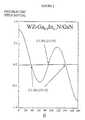
- FIG. 1illustrates the crystal structure of a WZ—GaN-based semiconductor.
- FIG. 2is a graph of the piezoelectric field generated in the quantum well with respect to the growth orientation of the WZ—GaN-based semiconductor quantum well.
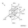
- FIG. 3illustrates the crystal structure of a ZB—GaN-based semiconductor.
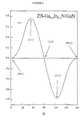
- FIG. 4is a graph of the piezoelectric field strength generated in the quantum well with respect to the first path shown in FIG. 3 .
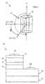
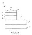
- FIG. 5is a cross-sectional view of a light-emitting device according to one embodiment of the present invention.
- FIG. 6is a graph of the relative light generation efficiency of quantum wells in a semiconductor device of the present invention and a prior art semiconductor device as functions of the well width.
- FIG. 7is a cross-sectional view of a light-emitting device according to a second embodiment of the present invention.
- FIG. 8is a cross-sectional view of a light-emitting device according to a third embodiment of the present invention.
- the present inventionis based in part on the observation that the piezoelectric field in a strained quantum well layer depends on the orientation of the crystal structure of the quantum well layer, and hence, by controlling the facet orientation, the piezoelectric field can be minimized.
- the manner in which this is accomplishedmay be more easily understood with reference to two types of strained quantum well structures, those based on a wurtzite crystal structure and those based on a zincblende crystal structure.
- FIG. 1illustrates a wurtzite crystal GaN (WZ—GaN) structure 10 .
- the piezoelectric field generated in a crystal having a facet orientation along arc 11 in FIG. 1is shown in FIG. 2 as a function of the angle ⁇ between the ⁇ 0001 ⁇ direction and the facet orientation.
- the data shown in FIG. 2is for Ga 0.9 In 0.1 N strained quantum well layers.
- the piezoelectric fieldreaches maxima in the ⁇ 0001 ⁇ direction or the ⁇ 000-1 ⁇ direction, and has three orientations at which the piezoelectric field is zero.
- the same resultis obtained for other arcs, e.g., arc 12 . That is, the piezoelectric field is uniquely determined by the difference in the angle between the ⁇ 0001 ⁇ direction and the facet orientation of the concerned plane, i.e., the piezoelectric field is independent of ⁇ .
- the planes at 90° to the c-axissuch as, for example, the a-plane, ⁇ 2-1-10 ⁇ , the m-plane ⁇ 0-110 ⁇ , etc.
- the planes around 40° and 140° to the c-axisalso provide planes with a zero piezoelectric field, e.g., the planes ⁇ 2-1-14 ⁇ , ⁇ 01-12 ⁇ , etc.
- the strength of the piezoelectric fielddepends on the strain in and the composition of the InGaN strained quantum well layer.
- the 90° facet orientation measured from the ⁇ 0001 ⁇ direction where the piezoelectric field becomes 0does not strongly depend on the ratio of Ga to In.
- the plane orientations corresponding to the 40° and 140° orientations discussed abovetypically change by no more than about of 5° from the 40° and 140° values determined for the composition shown in FIG. 2 .
- the present inventionis also based in part on the observation that the strength of the spontaneous electric field in a wurtzite crystal structure III-Nitride quantum well layer depends on the facet orientation of the quantum well layer, and hence the spontaneous electric field can also be minimized by controlling the facet orientation.
- the spontaneous electric fieldapproaches zero for a III-Nitride quantum well layer having approximately an a-plane or approximately an m-plane facet orientation.
- facet orientationsare tilted at angles of, for example, about 80° to about 90° with respect to the ⁇ 0001 ⁇ direction of the wurtzite crystal structure.
- the strength of the spontaneous electric fieldalso depends on the composition of the quantum well layer and on the composition of its adjacent layers.
- the piezoelectric fieldis typically much larger than the spontaneous electric field.
- the combination of the piezoelectric and spontaneous electric fieldsis dominated by the piezoelectric field, and it may be advantageous to select a facet orientation that minimizes the piezoelectric field.
- the spontaneous electric fieldmay be comparable to or even dominate the piezoelectric field.
- the spontaneous electric fielddominates the piezoelectric field, it may be advantageous to select a facet orientation that minimizes the spontaneous electric field. If the piezoelectric and spontaneous electric fields are comparable, it may be advantageous to select a facet orientation that minimizes the combined field but does not necessarily minimize either the spontaneous or piezoelectric fields separately.
- FIG. 3shows the crystal structure 20 of the ZB—GaN-based semiconductor.
- the radius vectorhas a polar angle ⁇ measured from the ⁇ 001 ⁇ direction and a cone angle, ⁇ about the ⁇ 001 ⁇ direction.
- First and second paths having a constant azimuth angleare shown at 21 and 22 .
- FIG. 4is a plot of the piezoelectric field in the strained quantum well layer with respect to the polar angle ⁇ for various orientations of the strained quantum well layer on path 21 .
- a strained quantum well crystal of ZB—GaN-based semiconductoralmost no piezoelectric field is generated in the strained quantum well layer that has growth planes beginning in the ⁇ 001 ⁇ plane or ⁇ 011 ⁇ plane and a facet orientation angle ⁇ on path 22 .
- a similar resultholds for planes that are equivalent to these.
- FIG. 5is a cross-sectional view of a light-emitting device 30 according to the present invention.
- Light-emitting device 30may be, e.g., a light-emitting diode or a laser diode. If the crystal growth orientation is excluded, the composition of each deposited layer is essentially that used in a conventional III-Nitride light-emitting device.
- Light-emitting device 30is constructed from a number of layers.
- An n-type GaN contact layer 33 , an n-type AlGaN cladding layer 34 , a strained multiple quantum well layer 35 , a p-type AlGaN cladding layer 36 , and a p-type GaN contact layer 37are successively deposited on a substrate 31 which is typically, AlN, SiC, or GaN.
- An n-electrode 38 and a p-electrode 39are deposited as shown.
- the strained multiple quantum well layer 35is typically constructed from GaInN/GaN or GaInN/GaInN.
- the layers of the quantum wellmay be caused to grow such that the piezoelectric field, the spontaneous electric field, or the combination of the piezoelectric field and the spontaneous electric field in the quantum well layer is negligible.
- the piezoelectric fieldis substantially zero.
- One of thesemay be utilized in a light-emitting device according to the present invention.
- the particular planewill depend on the type of crystal.
- the ⁇ 2-1-10 ⁇ plane of the strained quantum layer materialcan be caused to grow by selecting the appropriate growing surface of substrate 31 .
- the substrateis SiC, for example, the SiC may be cut such that the ⁇ 2-1-10 ⁇ plane is used for growing layer 33 .
- the choice of an a-plane (e.g., ⁇ 2-1-10 ⁇ ) or an m-plane facet orientationalso minimizes the spontaneous electric field and thus the combination of the piezoelectric and spontaneous electric fields.
- the relative efficiency of a light-emitting device according to the present invention(in which the combination of the piezoelectric and spontaneous electric fields is negligible) and a conventional light-emitting device including a quantum well having a ⁇ 0001 ⁇ facet orientation (such as a conventional device grown on the ⁇ 0001 ⁇ plane of a sapphire substrate, for example) is shown in FIG. 6 as a function of the width of the quantum well.
- Curve Ais the efficiency for the device discussed above with reference to FIG. 5
- curve Bis the efficiency of the conventional device. It will be appreciated from this figure that the present invention provides a substantial improvement in the efficiency of light generation.
- III-Nitride light-emitting devicesfrequently include a III-Nitride nucleation layer grown on the substrate by metal-organic chemical vapor deposition at a low temperature (typically less than about 800° C.) to accommodate lattice mismatch between the substrate and device layers grown above the nucleation layer. This is typically the case for devices grown on sapphire substrates, for example.
- low temperature III-Nitride nucleation layers and III-Nitride device layers grown above themtypically adopt a wurtzite crystal structure with a ⁇ 0001 ⁇ facet orientation regardless of the facet orientation of the substrate surface on which the layers are grown. As noted above, this leads to a high piezoelectric field and poor efficiency.
- light-emitting device 30includes a high temperature III-Nitride nucleation layer 32 in addition to the layers shown in FIG. 5 .
- High temperature III-Nitride nucleation layer 32is grown directly on substrate 31 by, e.g., metal-organic chemical vapor deposition at a temperature sufficiently high that the crystal structure of layer 32 substantially replicates that of the surface of substrate 31 on which layer 32 is grown.
- the facet orientation of high temperature nucleation layer 32 and of subsequently grown layersis substantially the same as that of the surface of substrate 31 . Consequently, the facet orientation of quantum wells in multiple quantum well layer 35 can be controlled by selecting the facet orientation of the surface of substrate 31 on which high temperature III-Nitride nucleation layer 32 is grown.
- Nucleation layer 32is typically grown at a temperature greater than about 800° C.
- the composition of nucleation layer 32may include, for example, nitrogen and any element or combination of elements from group III of the periodic table.
- the composition of nucleation layer 32is selected to have a lattice mismatch of less than about 10% with the surface of substrate 31 on which layer 32 is grown and with subsequently grown device layers.
- substrate 31is typically a non- ⁇ 0001 ⁇ orientation substrate chosen to have a lattice mismatch of less than about 10% with nucleation layer 32 .
- Suitable substrates in this embodimentinclude but are not limited to non- ⁇ 0001 ⁇ planes of SiC, AlN, and GaN as described above.
- FIG. 8shows n-type GaN contact layer 33 grown directly on high temperature nucleation layer 32
- additional layersmay include, for example, buffer layers and defect reduction layers.
- substrate 31is a SiC substrate having a growth surface with a facet orientation at an angle of about 40° from ⁇ 0001 ⁇
- high temperature nucleation layer 32is an Al x Ga 1 ⁇ x N layer with 0 ⁇ 1.
- nucleation layer 32is typically grown at a temperature of about 1000° C. to about 1200° C., more typically about 1100° C.
- the mole fraction x of Aluminum in nucleation layer 32is typically about 0.04 to about 1.0.
- the thickness of nucleation layer 32 in this implementationis typically about 100 Angstroms ( ⁇ ) to about 1 micron ( ⁇ m).
- III-Nitride light-emitting deviceson SiC substrates having growth surfaces with facet orientations at about 40° or about 140° from ⁇ 0001 ⁇ .
- the crystal structures of these facetsare more like the ⁇ 0001 ⁇ facet than are the a-planes and m-planes. Consequently, it may be easier to grow high quality III-Nitride crystals on SiC substrate facets oriented at about 40° or about 140° from ⁇ 0001 ⁇ than on SiC a-plane or m-plane facets.
- substrate 31is an AlN substrate having a growth surface with a facet orientation at an angle of about 90° from ⁇ 0001 ⁇ .
- the growth surfacemay be an a-plane or an m-plane, for example.
- nucleation layer 32may be formed from Al x Ga 1 ⁇ x N (0 ⁇ 1) typically grown at a temperature of about 1000° C. to about 1200° C., more typically about 1100° C.
- the mole fraction x of Aluminum in nucleation layer 32 and the thickness of layer 32may be as described in the above implementation, for example.
- the present inventionmay also be utilized to provide improved performance from photodetectors.
- Photodetectors fabricated by growing the device on the ⁇ 0001 ⁇ plane of a sapphire substrateexhibit an efficiency and absorption band that depend on light intensity. In particular, the efficiency of conversion increases with light intensity while the useful wavelength range decreases.
- the deviceis grown on a substrate that results in, for example, little or no piezoelectric field in the strained quantum well layer. Hence, the dependence of the efficiency and the absorption band on light intensity are substantially reduced or eliminated.
- the growing technique for a photodetectoris the same as that used to construct a light emitter, however, thicker strained quantum well layers are utilized to improve the absorption of the incident light.
- FIG. 7is a cross-sectional view of the optical semiconductor device 50 according to another embodiment of the present invention in which only the layers related solely to light emission and absorption have the desired facet orientation.
- Device 50is constructed by growing an n-type GaN contact layer 53 and an n-type AlGaN cladding layer 54 on the ⁇ 0001 ⁇ plane orientation on the substrate 51 such as SiC or GaN based on conventional technology.
- the ⁇ 2-1-14) plane or ⁇ 01-12 ⁇ planeis formed.
- the GaInN/GaN or GaInN/GaInN strained multiple quantum well layer 55is then formed by repeating the crystal growth.
- the remaining p-type Al GaN cladding layer 56 and the p-type GaN contact layer 57are successively deposited and formed.
- the p-type Al GaN cladding layer 56 and the p-type GaN contact layer 57change the crystal structure back to that corresponding to the ⁇ 0001 ⁇ plane from the facet orientation of the well layer 55 and become layers with specific thicknesses.
- the n-electrode 58 and the p-electrode 59are formed as the electrodes on the n-type GaN contact layer 53 and the p-type GaN contact layer 57 , respectively.
- the growing surfaces 55 A, 55 B on both sides of the GaInN strained multiple quantum well layer 55are, for example, the ⁇ 01-12 ⁇ plane or the ⁇ 2-1-14 ⁇ plane.
- the p-type AlGaN cladding layer 56 and the p-type GaN contact layer 57become flat growing surfaces. To simplify the next process, it is advisable that they be several microns thick.
- an AlN buffer layer 52is grown on the substrate 51 .
- the specific plane selected for growing the quantum well layerdepends on the crystal type.
- the piezoelectric field as a function of the facet orientationbehaves similarly to that described above if the crystal type is the same.
- the orientation inclination, ⁇ , for which the piezoelectric field is 0may, however, change by as much as 10°.
Landscapes
- Engineering & Computer Science (AREA)
- Physics & Mathematics (AREA)
- Condensed Matter Physics & Semiconductors (AREA)
- General Physics & Mathematics (AREA)
- Microelectronics & Electronic Packaging (AREA)
- Manufacturing & Machinery (AREA)
- Computer Hardware Design (AREA)
- Chemical & Material Sciences (AREA)
- Power Engineering (AREA)
- Crystallography & Structural Chemistry (AREA)
- Materials Engineering (AREA)
- Optics & Photonics (AREA)
- Nanotechnology (AREA)
- Electromagnetism (AREA)
- Life Sciences & Earth Sciences (AREA)
- Biophysics (AREA)
- Led Devices (AREA)
Abstract
Description
Claims (20)
Priority Applications (4)
| Application Number | Priority Date | Filing Date | Title |
|---|---|---|---|
| US09/992,192US6849472B2 (en) | 1997-09-30 | 2001-11-13 | Nitride semiconductor device with reduced polarization fields |
| TW091133134ATWI264132B (en) | 2001-11-13 | 2002-11-12 | Nitride semiconductor device with reduced polarization fields |
| JP2002329082AJP2003158297A (en) | 2001-11-13 | 2002-11-13 | Nitride semiconductor devices with reduced polarization field |
| DE10253082ADE10253082A1 (en) | 2001-11-13 | 2002-11-13 | Semiconductor light emitter and photodetector based on gallium nitride |
Applications Claiming Priority (5)
| Application Number | Priority Date | Filing Date | Title |
|---|---|---|---|
| JP09/265-311 | 1997-09-30 | ||
| JP26531197AJP3955367B2 (en) | 1997-09-30 | 1997-09-30 | Optical semiconductor device and manufacturing method thereof |
| US09/162,708US6229151B1 (en) | 1997-09-30 | 1998-09-29 | Group III-V semiconductor light emitting devices with reduced piezoelectric fields and increased efficiency |
| US09/717,647US6569704B1 (en) | 1997-09-30 | 2000-11-21 | Group III-V semiconductor light emitting devices with reduced piezoelectric fields and increased efficiency |
| US09/992,192US6849472B2 (en) | 1997-09-30 | 2001-11-13 | Nitride semiconductor device with reduced polarization fields |
Related Parent Applications (1)
| Application Number | Title | Priority Date | Filing Date |
|---|---|---|---|
| US09/717,647Continuation-In-PartUS6569704B1 (en) | 1997-09-30 | 2000-11-21 | Group III-V semiconductor light emitting devices with reduced piezoelectric fields and increased efficiency |
Publications (2)
| Publication Number | Publication Date |
|---|---|
| US20020084467A1 US20020084467A1 (en) | 2002-07-04 |
| US6849472B2true US6849472B2 (en) | 2005-02-01 |
Family
ID=25538024
Family Applications (1)
| Application Number | Title | Priority Date | Filing Date |
|---|---|---|---|
| US09/992,192Expired - LifetimeUS6849472B2 (en) | 1997-09-30 | 2001-11-13 | Nitride semiconductor device with reduced polarization fields |
Country Status (4)
| Country | Link |
|---|---|
| US (1) | US6849472B2 (en) |
| JP (1) | JP2003158297A (en) |
| DE (1) | DE10253082A1 (en) |
| TW (1) | TWI264132B (en) |
Cited By (22)
| Publication number | Priority date | Publication date | Assignee | Title |
|---|---|---|---|---|
| US20030198837A1 (en)* | 2002-04-15 | 2003-10-23 | Craven Michael D. | Non-polar a-plane gallium nitride thin films grown by metalorganic chemical vapor deposition |
| US20060202105A1 (en)* | 2005-03-14 | 2006-09-14 | Lumileds Lighting U.S., Llc | Wavelength-converted semiconductor light emitting device |
| US20060202215A1 (en)* | 2005-03-14 | 2006-09-14 | Lumileds Lighting U.S., Llc | Polarization-reversed III-nitride light emitting device |
| US20070080369A1 (en)* | 2005-10-06 | 2007-04-12 | Showa Denko K.K. | Group III nitride semiconductor stacked structure and production method thereof |
| US20070128844A1 (en)* | 2003-04-15 | 2007-06-07 | Craven Michael D | Non-polar (a1,b,in,ga)n quantum wells |
| US20070284616A1 (en)* | 2006-06-08 | 2007-12-13 | Samsung Electro-Mechanics Co., Ltd. | Light emitting transistor |
| US20080113496A1 (en)* | 2006-11-15 | 2008-05-15 | The Regents Of The University Of California | METHOD FOR HETEROEPITAXIAL GROWTH OF HIGH-QUALITY N-FACE GaN, InN, AND AlN AND THEIR ALLOYS BY METAL ORGANIC CHEMICAL VAPOR DEPOSITION |
| US20080135853A1 (en)* | 2002-04-15 | 2008-06-12 | The Regents Of The University Of California | Dislocation reduction in non-polar iii-nitride thin films |
| US20080283846A1 (en)* | 2007-05-18 | 2008-11-20 | Sony Corporation | Method for growing semiconductor layer, method for producing semiconductor light-emitting element, semiconductor light-emitting element, and electronic device |
| US20080308836A1 (en)* | 2005-01-27 | 2008-12-18 | Rohm Co., Ltd. | Nitride Semiconductor Device and Method for Growing Nitride Semiconductor Crystal Layer |
| US20090039356A1 (en)* | 2007-08-08 | 2009-02-12 | The Regents Of The University Of California | Planar nonpolar m-plane group iii-nitride films grown on miscut substrates |
| US20090246944A1 (en)* | 2006-11-15 | 2009-10-01 | The Regents Of The University Of California | METHOD FOR HETEROEPITAXIAL GROWTH OF HIGH-QUALITY N-FACE GaN, InN, AND AlN AND THEIR ALLOYS BY METAL ORGANIC CHEMICAL VAPOR DEPOSITION |
| US20100008393A1 (en)* | 2008-07-09 | 2010-01-14 | Sumitomo Electric Industries, Ltd. | Group iii nitride semiconductor light-emitting device and epitaxial wafer |
| WO2010016459A1 (en) | 2008-08-04 | 2010-02-11 | 住友電気工業株式会社 | Gan semiconductor optical element, method for manufacturing gan semiconductor optical element, epitaxial wafer and method for growing gan semiconductor film |
| US20100052008A1 (en)* | 2008-02-01 | 2010-03-04 | The Regents Of The University Of California | Enhancement of optical polarization of nitride light-emitting diodes by wafer off-axis cut |
| US20100220761A1 (en)* | 2009-03-02 | 2010-09-02 | Sumitomo Electric Industries, Ltd. | Gallium nitride-based semiconductor optical device, method of fabricating gallium nitride-based semiconductor optical device, and epitaxial wafer |
| US20100309943A1 (en)* | 2009-06-05 | 2010-12-09 | The Regents Of The University Of California | LONG WAVELENGTH NONPOLAR AND SEMIPOLAR (Al,Ga,In)N BASED LASER DIODES |
| US7956360B2 (en) | 2004-06-03 | 2011-06-07 | The Regents Of The University Of California | Growth of planar reduced dislocation density M-plane gallium nitride by hydride vapor phase epitaxy |
| US20110216795A1 (en)* | 2007-02-12 | 2011-09-08 | The Regents Of The University Of California | Semi-polar iii-nitride optoelectronic devices on m-plane substrates with miscuts less than +/-15 degrees in the c-direction |
| CN102496665A (en)* | 2011-12-14 | 2012-06-13 | 中微光电子(潍坊)有限公司 | Structure of silicon-substrate GaN-based light-emitting diode (LED) and manufacturing method for silicon-substrate GaN-based LED |
| US9543490B2 (en) | 2010-09-24 | 2017-01-10 | Seoul Semiconductor Co., Ltd. | Wafer-level light emitting diode package and method of fabricating the same |
| US10580929B2 (en) | 2016-03-30 | 2020-03-03 | Seoul Viosys Co., Ltd. | UV light emitting diode package and light emitting diode module having the same |
Families Citing this family (32)
| Publication number | Priority date | Publication date | Assignee | Title |
|---|---|---|---|---|
| US6888867B2 (en)* | 2001-08-08 | 2005-05-03 | Nobuhiko Sawaki | Semiconductor laser device and fabrication method thereof |
| US6943381B2 (en)* | 2004-01-30 | 2005-09-13 | Lumileds Lighting U.S., Llc | III-nitride light-emitting devices with improved high-current efficiency |
| US7408201B2 (en)* | 2004-03-19 | 2008-08-05 | Philips Lumileds Lighting Company, Llc | Polarized semiconductor light emitting device |
| US7808011B2 (en)* | 2004-03-19 | 2010-10-05 | Koninklijke Philips Electronics N.V. | Semiconductor light emitting devices including in-plane light emitting layers |
| JP2005340765A (en)* | 2004-04-30 | 2005-12-08 | Sumitomo Electric Ind Ltd | Semiconductor light emitting device |
| US9130119B2 (en)* | 2006-12-11 | 2015-09-08 | The Regents Of The University Of California | Non-polar and semi-polar light emitting devices |
| JP4513446B2 (en)* | 2004-07-23 | 2010-07-28 | 豊田合成株式会社 | Crystal growth method of semiconductor crystal |
| FI118196B (en)* | 2005-07-01 | 2007-08-15 | Optogan Oy | Semiconductor structure and method for producing a semiconductor structure |
| US7221000B2 (en)* | 2005-02-18 | 2007-05-22 | Philips Lumileds Lighting Company, Llc | Reverse polarization light emitting region for a semiconductor light emitting device |
| TWI377602B (en) | 2005-05-31 | 2012-11-21 | Japan Science & Tech Agency | Growth of planar non-polar {1-100} m-plane gallium nitride with metalorganic chemical vapor deposition (mocvd) |
| TWI455181B (en)* | 2005-06-01 | 2014-10-01 | Univ California | Growth and manufacturing techniques for semi-polar (Ga, Al, In, B) N films, heterostructures and devices |
| WO2007030709A2 (en)* | 2005-09-09 | 2007-03-15 | The Regents Of The University Of California | METHOD FOR ENHANCING GROWTH OF SEMI-POLAR (Al, In,Ga,B)N VIA METALORGANIC CHEMICAL VAPOR DEPOSITION |
| US8193079B2 (en) | 2006-02-10 | 2012-06-05 | The Regents Of The University Of California | Method for conductivity control of (Al,In,Ga,B)N |
| JP4984119B2 (en) | 2006-08-28 | 2012-07-25 | スタンレー電気株式会社 | Nitride semiconductor crystal or light emitting device using the same and method for manufacturing the same |
| JP2008130606A (en)* | 2006-11-16 | 2008-06-05 | Sony Corp | Semiconductor light emitting element and its manufacturing method, light source cell unit, backlight, lighting device, display, electronic device, and semiconductor element and its manufacturing method |
| EP2111634A4 (en)* | 2007-02-12 | 2014-01-08 | Univ California | NON-POLAR NITRIDE III LIGHT-EMITTING DIODES AND LIGHT-EMITTING DIODES, FREE OF AL (X) GA (1-X) N SHEATH |
| JP5050574B2 (en)* | 2007-03-05 | 2012-10-17 | 住友電気工業株式会社 | Group III nitride semiconductor light emitting device |
| KR100889956B1 (en)* | 2007-09-27 | 2009-03-20 | 서울옵토디바이스주식회사 | AC Light Emitting Diode |
| JP2009170798A (en)* | 2008-01-18 | 2009-07-30 | Sumitomo Electric Ind Ltd | Group III nitride semiconductor laser |
| JP5003527B2 (en) | 2008-02-22 | 2012-08-15 | 住友電気工業株式会社 | Group III nitride light emitting device and method for fabricating group III nitride semiconductor light emitting device |
| US20090238227A1 (en)* | 2008-03-05 | 2009-09-24 | Rohm Co., Ltd. | Semiconductor light emitting device |
| US7956369B2 (en)* | 2008-05-07 | 2011-06-07 | The United States Of America As Represented By The Secretary Of The Army | Light emitting diode |
| CN101874309B (en)* | 2008-09-11 | 2013-01-30 | 住友电气工业株式会社 | Nitride-based semiconductor optical element, epitaxial wafer for nitride-based semiconductor optical element, and method for manufacturing semiconductor light-emitting element |
| JP5316276B2 (en)* | 2009-01-23 | 2013-10-16 | 住友電気工業株式会社 | Nitride semiconductor light emitting device, epitaxial substrate, and method for manufacturing nitride semiconductor light emitting device |
| JP5265404B2 (en)* | 2009-02-04 | 2013-08-14 | パナソニック株式会社 | Nitride semiconductor light emitting device and manufacturing method thereof |
| JP5446622B2 (en)* | 2009-06-29 | 2014-03-19 | 住友電気工業株式会社 | Group III nitride crystal and method for producing the same |
| JP4835741B2 (en)* | 2009-09-30 | 2011-12-14 | 住友電気工業株式会社 | Method for fabricating a semiconductor light emitting device |
| RU2434315C1 (en)* | 2010-03-15 | 2011-11-20 | Юрий Георгиевич Шретер | Light-emitting device with heterophase boundaries |
| TWI416762B (en)* | 2010-08-23 | 2013-11-21 | Univ Nat Sun Yat Sen | Homogeneous heterogeneous quantum well |
| JP5948698B2 (en)* | 2012-04-13 | 2016-07-06 | パナソニックIpマネジメント株式会社 | Ultraviolet light emitting device and manufacturing method thereof |
| CN114023853A (en)* | 2021-11-05 | 2022-02-08 | 聚灿光电科技(宿迁)有限公司 | A kind of LED and preparation method thereof |
| CN115863505A (en)* | 2023-02-27 | 2023-03-28 | 北京大学 | Nitride light-emitting diode with three-dimensional structure and preparation method thereof |
Citations (13)
| Publication number | Priority date | Publication date | Assignee | Title |
|---|---|---|---|---|
| US4952792A (en)* | 1989-10-13 | 1990-08-28 | At&T Bell Laboratories | Devices employing internally strained asymmetric quantum wells |
| US5081519A (en)* | 1990-01-19 | 1992-01-14 | Mitsubishi Denki Kabushiki Kaisha | Semiconductor device |
| EP0716457A2 (en) | 1994-12-02 | 1996-06-12 | Nichia Chemical Industries, Ltd. | Nitride semiconductor light-emitting device |
| WO1996024167A1 (en) | 1995-02-03 | 1996-08-08 | Advanced Technology Materials, Inc. | High brightness electroluminescent device emitting in the green to ultraviolet spectrum, and method of making the same |
| US5561301A (en)* | 1994-02-21 | 1996-10-01 | Fujitsu Limited | Opto-semiconductor device with piezoelectric |
| EP0743727A1 (en) | 1995-05-19 | 1996-11-20 | Nec Corporation | GaN system semiconductor laser device |
| US5602418A (en)* | 1992-08-07 | 1997-02-11 | Asahi Kasei Kogyo Kabushiki Kaisha | Nitride based semiconductor device and manufacture thereof |
| US5625202A (en)* | 1995-06-08 | 1997-04-29 | University Of Central Florida | Modified wurtzite structure oxide compounds as substrates for III-V nitride compound semiconductor epitaxial thin film growth |
| US5727008A (en)* | 1995-05-19 | 1998-03-10 | Sanyo Electric Co., Ltd. | Semiconductor light emitting device, semiconductor laser device, and method of fabricating semiconductor light emitting device |
| US5880485A (en)* | 1997-03-24 | 1999-03-09 | Mitsubishi Denki Kabushiki Kaisha | Semiconductor device including Gallium nitride layer |
| US6229151B1 (en) | 1997-09-30 | 2001-05-08 | Agilent Technologies, Inc. | Group III-V semiconductor light emitting devices with reduced piezoelectric fields and increased efficiency |
| WO2001041224A2 (en) | 1999-12-02 | 2001-06-07 | Cree Lighting Company | High efficiency light emitters with reduced polarization-induced charges |
| WO2002003474A2 (en) | 2000-07-03 | 2002-01-10 | Nichia Corporation | N-type nitride semiconductor laminate and semiconductor device using same |
Family Cites Families (2)
| Publication number | Priority date | Publication date | Assignee | Title |
|---|---|---|---|---|
| US6233265B1 (en)* | 1998-07-31 | 2001-05-15 | Xerox Corporation | AlGaInN LED and laser diode structures for pure blue or green emission |
| US6355497B1 (en)* | 2000-01-18 | 2002-03-12 | Xerox Corporation | Removable large area, low defect density films for led and laser diode growth |
- 2001
- 2001-11-13USUS09/992,192patent/US6849472B2/ennot_activeExpired - Lifetime
- 2002
- 2002-11-12TWTW091133134Apatent/TWI264132B/ennot_activeIP Right Cessation
- 2002-11-13DEDE10253082Apatent/DE10253082A1/ennot_activeCeased
- 2002-11-13JPJP2002329082Apatent/JP2003158297A/enactivePending
Patent Citations (14)
| Publication number | Priority date | Publication date | Assignee | Title |
|---|---|---|---|---|
| US4952792A (en)* | 1989-10-13 | 1990-08-28 | At&T Bell Laboratories | Devices employing internally strained asymmetric quantum wells |
| US5081519A (en)* | 1990-01-19 | 1992-01-14 | Mitsubishi Denki Kabushiki Kaisha | Semiconductor device |
| US5602418A (en)* | 1992-08-07 | 1997-02-11 | Asahi Kasei Kogyo Kabushiki Kaisha | Nitride based semiconductor device and manufacture thereof |
| US5561301A (en)* | 1994-02-21 | 1996-10-01 | Fujitsu Limited | Opto-semiconductor device with piezoelectric |
| EP0716457A2 (en) | 1994-12-02 | 1996-06-12 | Nichia Chemical Industries, Ltd. | Nitride semiconductor light-emitting device |
| WO1996024167A1 (en) | 1995-02-03 | 1996-08-08 | Advanced Technology Materials, Inc. | High brightness electroluminescent device emitting in the green to ultraviolet spectrum, and method of making the same |
| EP0743727A1 (en) | 1995-05-19 | 1996-11-20 | Nec Corporation | GaN system semiconductor laser device |
| US5727008A (en)* | 1995-05-19 | 1998-03-10 | Sanyo Electric Co., Ltd. | Semiconductor light emitting device, semiconductor laser device, and method of fabricating semiconductor light emitting device |
| US5742628A (en)* | 1995-05-19 | 1998-04-21 | Nec Corporation | Short wavelength laser emitting diode with an improved GaN system double heterostructure |
| US5625202A (en)* | 1995-06-08 | 1997-04-29 | University Of Central Florida | Modified wurtzite structure oxide compounds as substrates for III-V nitride compound semiconductor epitaxial thin film growth |
| US5880485A (en)* | 1997-03-24 | 1999-03-09 | Mitsubishi Denki Kabushiki Kaisha | Semiconductor device including Gallium nitride layer |
| US6229151B1 (en) | 1997-09-30 | 2001-05-08 | Agilent Technologies, Inc. | Group III-V semiconductor light emitting devices with reduced piezoelectric fields and increased efficiency |
| WO2001041224A2 (en) | 1999-12-02 | 2001-06-07 | Cree Lighting Company | High efficiency light emitters with reduced polarization-induced charges |
| WO2002003474A2 (en) | 2000-07-03 | 2002-01-10 | Nichia Corporation | N-type nitride semiconductor laminate and semiconductor device using same |
Non-Patent Citations (26)
| Title |
|---|
| Akihiko Ishibashi et al., "Metalorganic Vapor Phase Epitaxy Growth of a High-Quality GaN/InGaN Single Quantum Well Structure Using a Misoriented SiC Substrate", Jpn. J. Appl. Phys. vol. 36 (1997), pp. 1961-1965. |
| Andreas Hanglieter, "The role of piezoelectric fields in GaN-based quantum wells", MRS Internet J. Nitride Semicond. Res. 3, 15 (1998) 1998-1999 The Materials Research Society, pp. 1-8. |
| Atsuko Niwa et al., "Valence subband structures of (1010)-GaN/AIGaN strained quantum wells calculated by the tight-binding method", Appl. Phys. Lett. 70 (16), Apr. 21, 1997, pp. 2159-2161. |
| D.A.B. Miller, D.S. Chemla et al., "Band-Edge Electoabsorption in Quantum Well Structures: The Quantum-Confined Stark Effect" Physical Review Letters, vol. 53, No. 22, Nov. 26, 1984, pp. 2173-2176. |
| D.L. Smith et al., "Piezoelectric effects in strained-layer superlattices", J. Appl. Phys. 63 (8), Apr. 15, 1998, pp. 2717-2719. |
| Dongjin Byun et al., "Optimization of the GaN-buffer growth on 6H-SiC(0001)", Thin Solid Films 289 (1996), pp. 256-260. |
| Edited by Shuji Nakamura and Shigefusa F. Chichibu, "Introduction to Nitride Semiconductor Blue Lasers and Light Emitting Diodes", First published 2000 by Taylor & Francis, 8 pp. |
| Fabio Bernardini et al., "Spontaneous polarization and piezoelectric constants of III-V nitrides", 1997 The American Physical Society, vol. 56, No. 16, Oct. 15, 1997-II, pp. R10 024-R10 027. |
| Fabio Della Sala, et al., "Free-carrier screening of polarization fields in wurtzite GaN/InGaN laser structures", Applied Physics Letters, vol. 74, No. 14, Apr. 5, 1999, pp. 2002-2004. |
| H. Amano, N. et al., "Metalorganic vapor phase epitaxial growth of a high quality GaN film using an AIN buffer layer", Appl. Phys. Lett. 48 (5), Feb. 3, 1986, pp. 353-355. |
| K. Domen et al., "Optical gain for wurtzite GaN with anisotropic strain in c plane", Appl. Phys. Lett 70 (8), Feb. 24, 1997, pp. 987-989. |
| K. Domen, "Analysis of polarization anisotropy along the c axis in the photoluminescence of wirtzite GaN" Appl. Phys. Lett. 71 (14), Oct. 6, 1997, 3 pp. |
| K. Horina et al., "Initial Growth Stage of AlGaN Grown Directly On (0001) 6H-SiC By MOVPE", Mat. Res. Soc. Symp. Proc. vol. 449 1997 Materials Research Society, pp. 73-78. |
| K. Horino et al. "Growth of (1100) Oriented GaN on (1100) 6H-SiC by Metalorganic Vapor Phase Epitaxy", International Symposium on Blue Laser and Light Emitting Diodes, Chiba Univ., Japan, Mar. 5-7, 1996, pp. 530-533. |
| L.H. Peng, et al., "Piezoelectric effects in the optical properties of strained InGaN quantum wells", Applied Physics Letters, vol. 74, No. 6, Feb. 8, 1999, pp. 795-797. |
| Noriyuki Kuwano et al., "Cross-sectional TEM study of microstructures in MOVPE GaN films grown on alpha-Al2O3 with a buffer layer of AIN", Journal of Crystal Growth 115 (1191), pp. 381-387. |
| S.F. Chichibu et al., "Effective band gap inhomogeneity and piezoelectric field in InGaN/GaN multiquantum well structures", Applied Physics Letters, vol. 73, No. 14, Oct. 5, 1998, pp. 2006-2008. |
| S.F. Chichibu et al., "Optical properties of InGaN quantum wells", Materials Science and Engineering B59 (1999), pp. 298-306. |
| Seoung-Hwan Park et al., "Crystal-orientation effects on the peizoelectric field and electronic properties of strained wurtzite semiconductors", Physical Review B, vol. 59, No. 7, Feb. 15, 1991-I, pp. 4725-4737. |
| Shuji Nakamura, "GaN Growth Using GaN Buffer Layer", Japanese Journal of Applied Physics vol. 30, No. 10A, Oct. 1991, pp. L1705-L1707. |
| Sun et al. "Piezoelectric Fields in Strained (In, Ga) As/GaAs Multiple-Quantum well Structures Grown on Vicinal (110) GaAs", Feb. 1994, IEEE, vol. 30, pp. 466-470.** |
| Takashi Mukai, et al., "Current and Temperature Dependences of Electoluminescence of InGaN-Based UV/Blue/Green Light-Emitting Diodes", Jpn. J. Appl. Phys. vol. 37 (1998), pp. L1358-L1361. |
| Tetsuya Takeuchi et al., "Determination of piezoelectric fields in strained GaInN quantum wells using the quantum-confined Stark effect", Applied Physics Letters, vol. 73, No. 12, Sep. 21, 1996, pp 1691-1693. |
| Tetsuya Takeuchi et al., "Quantum-Confined Stark Effect due to Piezoelectric Fields in GaInN Strained Quantum Wells", Jpn. J. Appl. Phys. vol. 36 (1997), pp. L382-L385, Part 2. No. 4A, Apr. 1, 1997. |
| Tetsuya Takeuchi et al., "Theoretical Study of Orientation Dependence of Piezoelectric Effects in Wurtzite Strained GaInN/GaN Heterstructures and Quantum Wells", Jpn. J. Appl. Phys. vol. 39 (2000) pp. 413-416, Part 1, No. 2A, Feb. 2000. |
| W.W. Chow, "Quantum-well width dependence of threshold current density in InGaN lasers", Applied Physics Letters, vol. 75, No. 2, Jul. 12, 1999, pp. 244-246. |
Cited By (51)
| Publication number | Priority date | Publication date | Assignee | Title |
|---|---|---|---|---|
| US20110229639A1 (en)* | 2002-04-15 | 2011-09-22 | The Regents Of The University Of California | Non-polar gallium nitride thin films grown by metalorganic chemical vapor deposition |
| US8809867B2 (en) | 2002-04-15 | 2014-08-19 | The Regents Of The University Of California | Dislocation reduction in non-polar III-nitride thin films |
| US20030198837A1 (en)* | 2002-04-15 | 2003-10-23 | Craven Michael D. | Non-polar a-plane gallium nitride thin films grown by metalorganic chemical vapor deposition |
| US9039834B2 (en) | 2002-04-15 | 2015-05-26 | The Regents Of The University Of California | Non-polar gallium nitride thin films grown by metalorganic chemical vapor deposition |
| US9893236B2 (en) | 2002-04-15 | 2018-02-13 | The Regents Of The University Of California | Non-polar (Al,B,In,Ga)N quantum wells |
| US20080135853A1 (en)* | 2002-04-15 | 2008-06-12 | The Regents Of The University Of California | Dislocation reduction in non-polar iii-nitride thin films |
| US20070128844A1 (en)* | 2003-04-15 | 2007-06-07 | Craven Michael D | Non-polar (a1,b,in,ga)n quantum wells |
| US7956360B2 (en) | 2004-06-03 | 2011-06-07 | The Regents Of The University Of California | Growth of planar reduced dislocation density M-plane gallium nitride by hydride vapor phase epitaxy |
| US20110193094A1 (en)* | 2004-06-03 | 2011-08-11 | The Regents Of The University Of California | Growth of planar reduced dislocation density m-plane gallium nitride by hydride vapor phase epitaxy |
| US20080308836A1 (en)* | 2005-01-27 | 2008-12-18 | Rohm Co., Ltd. | Nitride Semiconductor Device and Method for Growing Nitride Semiconductor Crystal Layer |
| US20060202105A1 (en)* | 2005-03-14 | 2006-09-14 | Lumileds Lighting U.S., Llc | Wavelength-converted semiconductor light emitting device |
| US20080121919A1 (en)* | 2005-03-14 | 2008-05-29 | Philips Lumileds Lighting Company Llc | Wavelength-Converted Semiconductor Light Emitting Device |
| US7341878B2 (en) | 2005-03-14 | 2008-03-11 | Philips Lumileds Lighting Company, Llc | Wavelength-converted semiconductor light emitting device |
| US8445929B2 (en) | 2005-03-14 | 2013-05-21 | Philips Lumileds Lighting Company Llc | Wavelength-converted semiconductor light emitting device |
| US7804100B2 (en) | 2005-03-14 | 2010-09-28 | Philips Lumileds Lighting Company, Llc | Polarization-reversed III-nitride light emitting device |
| US20060202215A1 (en)* | 2005-03-14 | 2006-09-14 | Lumileds Lighting U.S., Llc | Polarization-reversed III-nitride light emitting device |
| US20100200886A1 (en)* | 2005-03-14 | 2010-08-12 | Koninklijke Philips Electronics N.V. | Wavelength-converted semiconductor light emitting device |
| US20070080369A1 (en)* | 2005-10-06 | 2007-04-12 | Showa Denko K.K. | Group III nitride semiconductor stacked structure and production method thereof |
| US7951617B2 (en) | 2005-10-06 | 2011-05-31 | Showa Denko K.K. | Group III nitride semiconductor stacked structure and production method thereof |
| US20070284616A1 (en)* | 2006-06-08 | 2007-12-13 | Samsung Electro-Mechanics Co., Ltd. | Light emitting transistor |
| US8455885B2 (en) | 2006-11-15 | 2013-06-04 | The Regents Of The University Of California | Method for heteroepitaxial growth of high-quality N-face gallium nitride, indium nitride, and aluminum nitride and their alloys by metal organic chemical vapor deposition |
| US8193020B2 (en) | 2006-11-15 | 2012-06-05 | The Regents Of The University Of California | Method for heteroepitaxial growth of high-quality N-face GaN, InN, and AlN and their alloys by metal organic chemical vapor deposition |
| US20080113496A1 (en)* | 2006-11-15 | 2008-05-15 | The Regents Of The University Of California | METHOD FOR HETEROEPITAXIAL GROWTH OF HIGH-QUALITY N-FACE GaN, InN, AND AlN AND THEIR ALLOYS BY METAL ORGANIC CHEMICAL VAPOR DEPOSITION |
| US7566580B2 (en) | 2006-11-15 | 2009-07-28 | The Regents Of The University Of California | Method for heteroepitaxial growth of high-quality N-face GaN, InN, and AIN and their alloys by metal organic chemical vapor deposition |
| US20090246944A1 (en)* | 2006-11-15 | 2009-10-01 | The Regents Of The University Of California | METHOD FOR HETEROEPITAXIAL GROWTH OF HIGH-QUALITY N-FACE GaN, InN, AND AlN AND THEIR ALLOYS BY METAL ORGANIC CHEMICAL VAPOR DEPOSITION |
| US9917422B2 (en) | 2007-02-12 | 2018-03-13 | The Regents Of The University Of California | Semi-polar III-nitride optoelectronic devices on M-plane substrates with miscuts less than +/− 15 degrees in the C-direction |
| US9077151B2 (en) | 2007-02-12 | 2015-07-07 | The Regents Of The University Of California | Semi-polar III-nitride optoelectronic devices on M-plane substrates with miscuts less than +/-15 degrees in the C-direction |
| US20110216795A1 (en)* | 2007-02-12 | 2011-09-08 | The Regents Of The University Of California | Semi-polar iii-nitride optoelectronic devices on m-plane substrates with miscuts less than +/-15 degrees in the c-direction |
| US20080283846A1 (en)* | 2007-05-18 | 2008-11-20 | Sony Corporation | Method for growing semiconductor layer, method for producing semiconductor light-emitting element, semiconductor light-emitting element, and electronic device |
| US8242513B2 (en) | 2007-05-18 | 2012-08-14 | Sony Corporation | Method for growing semiconductor layer, method for producing semiconductor light-emitting element, semiconductor light-emitting element, and electronic device |
| US20170327969A1 (en)* | 2007-08-08 | 2017-11-16 | The Regents Of The University Of California | Planar nonpolar group iii-nitride films grown on miscut substrates |
| US20110237054A1 (en)* | 2007-08-08 | 2011-09-29 | The Regents Of The University Of California | Planar nonpolar group iii-nitride films grown on miscut substrates |
| US20090039356A1 (en)* | 2007-08-08 | 2009-02-12 | The Regents Of The University Of California | Planar nonpolar m-plane group iii-nitride films grown on miscut substrates |
| US8278128B2 (en) | 2008-02-01 | 2012-10-02 | The Regents Of The University Of California | Enhancement of optical polarization of nitride light-emitting diodes by wafer off-axis cut |
| US20100052008A1 (en)* | 2008-02-01 | 2010-03-04 | The Regents Of The University Of California | Enhancement of optical polarization of nitride light-emitting diodes by wafer off-axis cut |
| US20100008393A1 (en)* | 2008-07-09 | 2010-01-14 | Sumitomo Electric Industries, Ltd. | Group iii nitride semiconductor light-emitting device and epitaxial wafer |
| WO2010016459A1 (en) | 2008-08-04 | 2010-02-11 | 住友電気工業株式会社 | Gan semiconductor optical element, method for manufacturing gan semiconductor optical element, epitaxial wafer and method for growing gan semiconductor film |
| US20110124142A1 (en)* | 2008-08-04 | 2011-05-26 | Sumitomo Electric Industries, Ltd. | Gan semiconductor optical element, method for manufacturing gan semiconductor optical element, epitaxial wafer and method for growing gan semiconductor film |
| US20100276663A1 (en)* | 2008-08-04 | 2010-11-04 | Sumitomo Electric Industries, Ltd. | Gan semiconductor optical element, method for manufacturing gan semiconductor optical element, epitaxial wafer and method for growing gan semiconductor film |
| US8228963B2 (en) | 2009-03-02 | 2012-07-24 | Sumitomo Electric Industries, Ltd. | Gallium nitride-based semiconductor optical device, method of fabricating gallium nitride-based semiconductor optical device, and epitaxial wafer |
| US20100220761A1 (en)* | 2009-03-02 | 2010-09-02 | Sumitomo Electric Industries, Ltd. | Gallium nitride-based semiconductor optical device, method of fabricating gallium nitride-based semiconductor optical device, and epitaxial wafer |
| EP2226858A2 (en) | 2009-03-02 | 2010-09-08 | Sumitomo Electric Industries, Ltd. | Gallium nitride-based semiconductor optical device, method of fabricating gallium nitride-based semiconductor optical device, and epitaxial wafer |
| US20100309943A1 (en)* | 2009-06-05 | 2010-12-09 | The Regents Of The University Of California | LONG WAVELENGTH NONPOLAR AND SEMIPOLAR (Al,Ga,In)N BASED LASER DIODES |
| US11552452B2 (en) | 2010-03-04 | 2023-01-10 | The Regents Of The University Of California | Semi-polar III-nitride optoelectronic devices on m-plane substrates with miscuts less than +/− 15 degrees in the c-direction |
| US9543490B2 (en) | 2010-09-24 | 2017-01-10 | Seoul Semiconductor Co., Ltd. | Wafer-level light emitting diode package and method of fabricating the same |
| US9882102B2 (en) | 2010-09-24 | 2018-01-30 | Seoul Semiconductor Co., Ltd. | Wafer-level light emitting diode and wafer-level light emitting diode package |
| US10069048B2 (en) | 2010-09-24 | 2018-09-04 | Seoul Viosys Co., Ltd. | Wafer-level light emitting diode package and method of fabricating the same |
| US10879437B2 (en) | 2010-09-24 | 2020-12-29 | Seoul Semiconductor Co., Ltd. | Wafer-level light emitting diode package and method of fabricating the same |
| US10892386B2 (en) | 2010-09-24 | 2021-01-12 | Seoul Semiconductor Co., Ltd. | Wafer-level light emitting diode package and method of fabricating the same |
| CN102496665A (en)* | 2011-12-14 | 2012-06-13 | 中微光电子(潍坊)有限公司 | Structure of silicon-substrate GaN-based light-emitting diode (LED) and manufacturing method for silicon-substrate GaN-based LED |
| US10580929B2 (en) | 2016-03-30 | 2020-03-03 | Seoul Viosys Co., Ltd. | UV light emitting diode package and light emitting diode module having the same |
Also Published As
| Publication number | Publication date |
|---|---|
| JP2003158297A (en) | 2003-05-30 |
| DE10253082A1 (en) | 2003-05-28 |
| US20020084467A1 (en) | 2002-07-04 |
| TWI264132B (en) | 2006-10-11 |
| TW200306017A (en) | 2003-11-01 |
Similar Documents
| Publication | Publication Date | Title |
|---|---|---|
| US6849472B2 (en) | Nitride semiconductor device with reduced polarization fields | |
| US6569704B1 (en) | Group III-V semiconductor light emitting devices with reduced piezoelectric fields and increased efficiency | |
| US6100106A (en) | Fabrication of nitride semiconductor light-emitting device | |
| JP4714401B2 (en) | Nucleation layers for improved light extraction from light emitting devices | |
| US7125736B2 (en) | Method of crystallizing a nitride III-V compound semiconductor layer on a sapphire substrate | |
| US6069394A (en) | Semiconductor substrate, semiconductor device and method of manufacturing the same | |
| US6693307B2 (en) | Semiconductor light emitting element | |
| JP3304782B2 (en) | Semiconductor light emitting device | |
| US6198112B1 (en) | III-V compound semiconductor luminescent device | |
| US20100096615A1 (en) | Light-emitting device | |
| US7285799B2 (en) | Semiconductor light emitting devices including in-plane light emitting layers | |
| EP2037508A1 (en) | ZnO-BASED SEMICONDUCTOR ELEMENT | |
| US20080283822A1 (en) | Semiconductor light emitting device | |
| US5843227A (en) | Crystal growth method for gallium nitride films | |
| US8878211B2 (en) | Heterogeneous substrate, nitride-based semiconductor device using same, and manufacturing method thereof | |
| JP3522114B2 (en) | Semiconductor light emitting device, method of manufacturing the same, and method of forming ZnO film | |
| JP3119200B2 (en) | Crystal growth method for nitride-based compound semiconductor and gallium nitride-based light emitting device | |
| US6525345B1 (en) | Semiconductor photonic device | |
| US20240413191A1 (en) | Variable composition ternary compound semiconductor alloys, structures, and devices | |
| US7875961B2 (en) | Semiconductor substrate of GaAs and semiconductor device | |
| JP2918139B2 (en) | Gallium nitride based compound semiconductor light emitting device | |
| CN101147303B (en) | Gallium nitride compound semiconductor laser element and manufacturing method therefor | |
| JP2976951B2 (en) | Display device with nitride semiconductor light emitting diode | |
| JPH11243228A (en) | Semiconductor element and method for manufacturing the same | |
| JPH10125957A (en) | Group III nitride semiconductor device and method of manufacturing the same |
Legal Events
| Date | Code | Title | Description |
|---|---|---|---|
| AS | Assignment | Owner name:LUMILEDS LIGHTING, U.S., LLC, CALIFORNIA Free format text:ASSIGNMENT OF ASSIGNORS INTEREST;ASSIGNOR:KRAMES, MICHAEL R.;REEL/FRAME:012325/0651 Effective date:20011107 | |
| STCF | Information on status: patent grant | Free format text:PATENTED CASE | |
| FPAY | Fee payment | Year of fee payment:4 | |
| AS | Assignment | Owner name:PHILIPS LUMILEDS LIGHTING COMPANY LLC, CALIFORNIA Free format text:CHANGE OF NAME;ASSIGNORS:LUMILEDS LIGHTING U.S., LLC;LUMILEDS LIGHTING, U.S., LLC;LUMILEDS LIGHTING, U.S. LLC;AND OTHERS;REEL/FRAME:025850/0770 Effective date:20110211 | |
| FPAY | Fee payment | Year of fee payment:8 | |
| FPAY | Fee payment | Year of fee payment:12 | |
| AS | Assignment | Owner name:DEUTSCHE BANK AG NEW YORK BRANCH, AS COLLATERAL AGENT, NEW YORK Free format text:SECURITY INTEREST;ASSIGNOR:LUMILEDS LLC;REEL/FRAME:043108/0001 Effective date:20170630 Owner name:DEUTSCHE BANK AG NEW YORK BRANCH, AS COLLATERAL AG Free format text:SECURITY INTEREST;ASSIGNOR:LUMILEDS LLC;REEL/FRAME:043108/0001 Effective date:20170630 | |
| AS | Assignment | Owner name:LUMILEDS LLC, CALIFORNIA Free format text:CHANGE OF NAME;ASSIGNOR:PHILIPS LUMILEDS LIGHTING COMPANY, LLC;REEL/FRAME:046111/0261 Effective date:20150326 |