US6849471B2 - Barrier layers for microelectromechanical systems - Google Patents
Barrier layers for microelectromechanical systemsDownload PDFInfo
- Publication number
- US6849471B2 US6849471B2US10/402,789US40278903AUS6849471B2US 6849471 B2US6849471 B2US 6849471B2US 40278903 AUS40278903 AUS 40278903AUS 6849471 B2US6849471 B2US 6849471B2
- Authority
- US
- United States
- Prior art keywords
- layer
- barrier layer
- sacrificial
- sacrificial layer
- transition metal
- Prior art date
- Legal status (The legal status is an assumption and is not a legal conclusion. Google has not performed a legal analysis and makes no representation as to the accuracy of the status listed.)
- Expired - Lifetime
Links
Images


Classifications
- B—PERFORMING OPERATIONS; TRANSPORTING
- B81—MICROSTRUCTURAL TECHNOLOGY
- B81C—PROCESSES OR APPARATUS SPECIALLY ADAPTED FOR THE MANUFACTURE OR TREATMENT OF MICROSTRUCTURAL DEVICES OR SYSTEMS
- B81C1/00—Manufacture or treatment of devices or systems in or on a substrate
- B81C1/00777—Preserve existing structures from alteration, e.g. temporary protection during manufacturing
- B81C1/00785—Avoid chemical alteration, e.g. contamination, oxidation or unwanted etching
- B81C1/00793—Avoid contamination, e.g. absorption of impurities or oxidation
- B—PERFORMING OPERATIONS; TRANSPORTING
- B81—MICROSTRUCTURAL TECHNOLOGY
- B81B—MICROSTRUCTURAL DEVICES OR SYSTEMS, e.g. MICROMECHANICAL DEVICES
- B81B2201/00—Specific applications of microelectromechanical systems
- B81B2201/04—Optical MEMS
- B81B2201/042—Micromirrors, not used as optical switches
- B—PERFORMING OPERATIONS; TRANSPORTING
- B81—MICROSTRUCTURAL TECHNOLOGY
- B81C—PROCESSES OR APPARATUS SPECIALLY ADAPTED FOR THE MANUFACTURE OR TREATMENT OF MICROSTRUCTURAL DEVICES OR SYSTEMS
- B81C2201/00—Manufacture or treatment of microstructural devices or systems
- B81C2201/05—Temporary protection of devices or parts of the devices during manufacturing
- B81C2201/053—Depositing a protective layers
Definitions
- the present inventionis related generally to microelectromechanical systems, and, more particularly, to fabricating microelectromechanical systems using barrier layers
- the present inventionprovides a method of fabricating microelectromechanical systems.
- the methodprecludes interaction and diffusion of sacrificial layers with structure layers of microelectromechanical systems by depositing selected barrier materials between structure and sacrificial layers.
- the barrier materialscan be either removed along with the sacrificial materials during the releasing process or kept along with the structure layers of the system after releasing.
- a methodcomprises: depositing a first sacrificial layer, depositing a first barrier layer after the first sacrificial layer, forming a structural layer of a microelectromechanical device after the first barrier layer; releasing the microelectromechanical device by removing the first sacrificial layer and the first barrier layer; and wherein the first barrier layer prevents diffusion and reaction between the first sacrificial layer and the structural layer.
- the methodfurther comprises: before releasing the microelectromechanical device by removing the first sacrificial layer and the first barrier layer, depositing a second barrier layer after the structural layer formed on the first barrier layer; depositing a second sacrificial layer after the second barrier layer; forming one or more structure layers of the microelectromechanical device after the second sacrificial layer; and wherein the second barrier layer prevents diffusion and interaction between the second sacrificial layer and the structural layer formed underneath the second barrier layer; and wherein the step of releasing the microelectromechanical device by removing the first sacrificial layer and the first barrier layer further comprises: removing the second sacrificial layer and the second barrier layer.
- the methodfurther comprises: before releasing the microelectromechanical device by removing the first sacrificial layer and the first barrier layer, depositing a second barrier layer after the structural layer formed on the first barrier layer; depositing a second sacrificial layer after the second barrier layer; forming one or more structural layers of the microelectromechanical device after the second sacrificial layer; and wherein the second barrier layer prevents diffusion and interaction between the second sacrificial layer and the structure layer formed underneath the second barrier layer; and wherein the step of releasing the microelectromechanical device by removing the first sacrificial layer and the first barrier layer further comprises: removing the second sacrificial layer, and wherein the second barrier layer is not removed after releasing the microelectromechanical device.
- a methodin another embodiment, comprises: depositing a first sacrificial layer; depositing a first barrier layer after the first sacrificial layer; patterning the first barrier layer, forming a structural layer of a microelectromechanical device after the patterned first barrier layer, releasing the microelectromechanical device by removing the first sacrificial layer; and wherein the first barrier layer prevents diffusion and reaction between the first sacrificial layer and the structural layer, and the first barrier layer is not removed after releasing the microelectromechanical device.
- the method of said embodiment of the inventionfurther comprises: before releasing the microelectromechanical device by removing the first sacrificial layer, depositing a second barrier layer after the structural layer formed on the first barrier layer; depositing a second sacrificial layer after the second barrier layer; forming one or more structure layers of the microelectromechanical device after the second sacrificial layer; and wherein the second barrier layer prevents diffusion and interaction between the second sacrificial layer and the structural layer formed underneath the second barrier layer; and wherein the step of releasing the microelectromechanical device by removing the first sacrificial layer further comprises: removing the second sacrificial layer and the second barrier layer.
- the method of said embodiment of the inventionfurther comprises: before releasing the microelectromechanical device by removing the first sacrificial layer, depositing a second barrier layer after the structural layer formed on the first barrier layer; depositing a second sacrificial layer after the second barrier layer; forming one or more structural layers of the microelectromechanical device after the second sacrificial layer; and wherein the second barrier layer prevents diffusion and interaction between the second sacrificial layer and the structure layer formed underneath the second barrier layer; and wherein the step of releasing the microelectromechanical device by removing the first sacrificial layer further comprises: removing the second sacrificial layer; and wherein the second barrier layer is not removed after releasing the microelectromechanical device.
- a methodcomprises: providing a substrate, on which a first sacrificial layer with a target thickness can be deposited; depositing the first sacrificial layer at a thickness less than the target thickness; measuring a thickness of the deposited first sacrificial layer; and depositing a second sacrificial layer with a thickness substantially equal to the difference between the target thickness and the measured thickness of the deposited first sacrificial layer.
- FIG. 1is a cross-sectional view of a structure illustrating a barrier layer formed between a structural layer of a microelectromechanical device and a sacrificial layer according to an embodiment of the invention
- FIG. 2 ais a cross-sectional view of a structure illustrating a barrier layer formed between a structural layer of a microclectromechanical device and a sacrificial layer according to another embodiment of the invention
- FIG. 2 bis a cross-sectional view of a structure illustrating a barrier layer formed between a structural layer of a microelectromechanical device and a sacrificial layer according to yet another embodiment of the invention
- FIG. 3is a cross-sectional view of a structure illustrating a barrier layer formed between a structural layer of a microelectromechanical device and a sacrificial layer according to a further embodiment of the invention
- FIG. 4 ais a cross-sectional view of a structure illustrating two barrier layers formed between a structural layer of a microelectromechanical device and two sacrificial layers according to yet another embodiment of the invention
- FIG. 4 bis a cross-sectional view of a structure illustrating two barrier layers formed between a structural layer of a microelectromechanical device and two sacrificial layers according to still yet another embodiment of the invention
- FIG. 5is a cross-sectional view of a structural illustrating a barrier layer deposited on a sacrificial layer for compensating the decrease of the sacrificial layer after deposition;
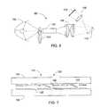
- FIG. 6is diagram illustrating an exemplary display system employing a spatial light modulator
- FIG. 7is a cross-sectional view of a portion of the spatial light modulator used in the display system of FIG. 6 and a portion of an array of micro-mirrors comprised in the spatial light modulator;
- FIG. 8 ais a cross-sectional views of a micromirror device of FIG. 7 before patterning the hinge layers during an exemplary fabrication process
- FIG. 8 bis a cross-sectional view of FIG. 8 a after patterning the hinge layers
- FIG. 9is the cross-sectional view of FIG. 8 b after removing the sacrificial and barrier layers
- FIG. 10 ashows an exemplary micromirror device after releasing
- FIG. 10 bpresents an exemplary micromirror array comprising a plurality of micromirrors of FIG. 10 a;
- FIG. 11 ais a back-view of another exemplary micromirror device after releasing
- FIG. 11 bis a back-view of a micromirror array comprising a plurality of micromirrors of FIG. 11 a;
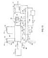
- FIG. 12is a diagram showing an exemplary etching system used in the embodiments of the invention.
- FIG. 13is a diagram showing another exemplary etching system used in the embodiments of the invention.
- FIG. 14 ais a side elevation view of an exemplary reciprocating pump for use in the exemplary etching system of FIG. 13 ;
- FIG. 14 bis a pump flow diagram of the reciprocating pump of FIG. 14 a together with associated flow lines and shutoff valves;
- FIG. 15is another exemplary etching system used in the embodiments of the present invention.
- the present inventionprovides a barrier layer that comprises selected barrier material(s) between a structure layer of the microelectromechanical device and a sacrificial layer during fabrication process.
- the barrier layerprevents diffusion and interaction between the sacrificial layer and the structure layer.
- the material for the barrier layeris selected depending upon detailed fabrication process. Specifically, the barrier material can be selected such that the barrier layer is removed with the sacrificial layer after releasing the microelectromechanical device. Alternatively, the barrier material can be such one that the barrier layer is not removed with the sacrificial layer after releasing.
- a barrier layeris deposited on a deposited sacrificial layer for compensating the deposition thickness inaccuracy of the deposited sacrificial layer.
- a barrier layeris deposited between a sacrificial layer and a structure layer of a microelectromechanical device, as shown in FIG. 1 .
- layer 132is a sacrificial layer deposited on substrate 120 for building desired structures of a microelectromechanical (MEMS) device during a fabrication process
- layer 136is a structure layer of the device. If the structure layer 136 is directly deposited on the sacrificial layer 132 , the material of the structural layer may sometimes diffuse into the sacrificial layer and/or interact with the material of the sacrificial layer, or vice versa. Such diffusion and interaction can deteriorate desired properties of the structure layer and expected performances of the MEMS device.
- barrier layer 134is provide between the sacrificial layer and the structure layer.
- the barrier layeris deposited on the sacrificial layer, and the structure layer is deposited on the barrier layer, as shown in the figure.
- the barrier layercomprises one or more barrier materials that are different from the sacrificial layer 132 .
- a preferred barrier layeris a layer that, in addition to preventing diffusion and interaction between the sacrificial and structure layers, there is substantially no diffusion and interaction between the two layers (e.g. the barrier layer and the given structure layer).
- no diffusion between two layersit is meant that no material from a first layer diffuses into a second layer, and no material from the second layer diffuses into the first layer.
- the ideal barrier layeris a layer that substantially has no interaction and diffusion between the barrier layer and the sacrificial layer. Otherwise, the residue(s) of the interaction or diffusion of between the barrier layer and the sacrificial layer may not be removable with the sacrificial layer.
- Such ideal materialsmay not be promptly available for many currently used structure materials, such as aluminum, especially when the non-diffusion and non-interaction property requirements is to be balanced with other requirements on, for example, electrical and/or mechanical properties of the barrier layer.
- Other materials that neither diffuse into nor interact with the structure layer during a certain time periode.g. time elapsed from the deposition of the structural layer and to the removal of the sacrificial layer) under a certain temperature (e.g. highest temperature during the fabrication time period) are also preferred because the deterioration resulting from the diffusion and interaction may only happen during the fabrication process and above certain processing temperatures.
- a certain temperaturee.g. highest temperature during the fabrication time period
- barrier layer 134is removed with the sacrificial layers. It is worthwhile to point out that barrier layer can be removed along with the sacrificial layer using one etching step. In this case, the barrier material for the barrier layer is removable in the etching process (and the etchant) that is selected for removing the sacrificial layer. Alternatively, the barrier layer and the sacrificial layer can be removed using separate etching steps, but not necessarily in this order.
- a second barrier layer 142is deposited after structure layer 136 , as shown in FIG. 2 a .
- the second barrier layeris deposited on the structure layer and covers the structure layer, including the vertical edges of the structure layer. By doing so, possibilities of diffusion and interaction between the edges of the structure layer and the sacrificial layer are eliminated. It is further preferred that the second barrier layer is provided when the second sacrificial layer needs to be deposited.
- Second barrier layer 142can be used without second sacrificial layer 138 , such as when there is a time period lag between depositing the layers and later (e.g. at a different location), releasing the MEMS device. In this case, these layers act as a protecting film in the interim.
- the second barrier layerprevents diffusion and interaction between structure layer 136 and the second sacrificial layer 138 , if present.
- Layer 142is preferably a layer that there is substantially no diffusion and interaction, or substantially no diffusion and interaction within a certain time period (e.g. fabrication duration) and under a certain temperature (e.g. the highest temperature during fabrication) between structure layer 136 and barrier layer 142 .
- the second barrier layer 142is removed with sacrificial layers 132 and 138 . Similar to barrier layer 134 , barrier layer 142 can be removed along with the sacrificial layers using one etching step. Alternatively, the second barrier layer can be removed by a separate etching step from that for sacrificial layers.
- the second barrier layer 142is not removed after releasing, as shown in FIG. 2 b .
- the second sacrificial layer 142may be patterned according to the structure layer and remains with structure layer 136 after releasing.
- the patterned barrier layercovers, in addition to the surfaces of the structure layer, the vertical edges of the structure layer.
- the second barrier layercomprises a different barrier material from that of the first barrier layer.
- the barrier material for the second barrier layeris not removable using the etching method(s) selected for removing the sacrificial layers and the first barrier layer, either in one etching step or in separate etching steps.
- a first barrier layer 140is deposited between the structure layer and the first sacrificial layer for preventing the diffusion and interaction between the first sacrificial layer 132 and structure layer 136 , as shown in FIG. 3 .
- barrier layer 140unlike barrier layer 134 , barrier layer 140 neither interacts with nor diffuses into structure layer 136 , or barrier layer 140 neither interacts with nor diffuses into structure layer 136 within a certain time period (e.g. fabrication duration) and under a certain temperature (e.g. the highest temperature in fabrication process).
- the first barrier layer 140is not removed after releasing the microelectromechanical device by removing the sacrificial layers.
- the first barrier layer 140is patterned after its deposition according to the structure layer formed thereon afterwards and remains after the releasing.
- the material of the first barrier layer 140is not removable using the etching method selected for removing the sacrificial layer 132 .
- a second sacrificial layer 138may be deposited as appropriate for forming other structure layers of the microelectromechanical device.
- a second barrier layer 142may be deposited on the formed structure layer 136 , as shown in FIG. 4 a .
- the second barrier layer 136is provided for preventing the diffusion and interaction between structure layer 136 and the second sacrificial layer 138 . It is preferred that the second barrier 142 neither interacts with nor diffuses into structure layer 136 , or neither interacts with not diffuses into structure layer 136 within a certain time period (e.g. fabrication duration) and under a certain temperature (e.g. the highest temperature in the fabrication process).
- the second barrier layer 142is patterned according to structure layer 136 and remains after the releasing.
- the barrier material of the second barrier layeris not removable using the etching method (including the etchant) selected for removing the sacrificial layers ( 132 and 138 ).
- the patterned barrier layeralso covers, in addition to the surfaces of the structure layer, the vertical edges of the structure layer.
- the barrier material of the second barrier layer 142is not necessarily the same as that of the first barrier layer 134 .
- the second barrier layer 142is removed along with the sacrificial layers after releasing, as shown in FIG. 4 b .
- the second barrier layeris deposited on the structure layer.
- the deposited second barrier layercovers, in addition to the surfaces of the structure layer, the vertical edges of the structure layer.
- the second barrier layeris preferably a material that neither interacts with not diffuses into structure layer 136 , or neither interacts with not diffuses into structure layer 136 within a certain time period (e.g. fabrication duration) and under a certain temperature (e.g. the highest temperature in the fabrication process), but it is removable using the etching method (including the etchant) selected for removing the sacrificial layers.
- the second barrier layercan be removed at a separate etching step than that for the sacrificial layers.
- the samples above where two sacrificial layers are depositedcan be where a micromirror plate 136 is on one sacrificial layer, and hinges are formed on the second sacrificial layer, such as will be described in reference to FIG. 8 a and FIG. 8 b.
- a barrier layercan be applied to compensate the deposition thickness inaccuracy of a deposited sacrificial layer.
- sacrificial layer 132 with a total target thickness, represented by His desired on substrate 144 during a fabrication process for a microelectromechanical device (not shown).
- H′the thickness of the deposited sacrificial layer
- H′ ⁇ Hthe target thickness
- barrier layer 146is deposited on the sacrificial layer after measuring the thickness of the deposited sacrificial layer. Barrier layer 146 can be removed with layer 132 or separately from layer 132 .
- the display systemcomprises light source 102 , optical devices (e.g. light pipe 104 , lens 106 and 108 ), color wheel 103 , display target 112 and spatial light modulator 110 .
- Light source 102e.g. an arc lamp
- directs incident light through the color wheel and optical devicese.g. light pipe 104 and object lens 106
- Spatial light modulator 110selectively reflects the incident light toward optical device 108 and results in an image on display target 112 .
- the display systemcan be operated in many ways, such as those set forth in U.S. Pat. No. 6,388,661, and U.S. patent application Ser. No. 10/340,162, filed on Jan. 10, 2003, both to Richards, the subject matter of each being incorporated herein by reference.
- light source 102In another exemplary display system (not shown), light source 102 , optical elements 104 , 106 and 108 , and display target 112 , as shown in FIG. 6 , are provided, while color wheel 103 is removed.
- three spatial light modulatorsare provided with each spatial light modulator being designated for modulating one of the three primary colors. Specifically, incident light from the light source is split, for example by a prism, into green, blue and red light. Each light impinges one of the three spatial light modulators and is modulated. The modulated light from all three spatial light modulators are then mapped onto the display target properly for displaying color images.
- the spatial light modulator of the systemgenerally comprises an array of thousands or millions of micro-mirrors, a portion of a cross-sectional view of which is illustrated in FIG. 7 .
- an array of micromirrorse.g. micromirrors 122
- a substrate 120such as glass that is transparent to visible light.
- Substrate 124which comprises an array of electrodes (e.g. electrode 126 ) and circuitry (not shown), is placed proximate to the array of micromirrors for electrostatically controlling the motion of the micromirrors.
- each individual micromirrorcan be deformed as desired under the control of one or more electrodes and circuitry; thereby the spatial modulation of the incident light traveling through substrate 120 and shining on the surfaces of the micromirrors can be achieved.
- micromirror devicessuch as micromirror device 130 can be fabricated in many ways, such as those set forth in U.S. Pat. Nos. 5,835,256 and 6,046,840 both to Huibers, and U.S. patent application Ser. No. 10/366,297 filed on Feb. 12, 2003 to Patel.
- An exemplary fabrication method according to embodiments of the present inventionwill be discussed in the following with references to FIG. 8 a through FIG. 9 .
- First sacrificial layer 132is deposited on the substrate followed by a deposition of a first barrier layer 134 , on which micromirror plate layer 136 is deposited thereafter.
- the substratecan be a glass (e.g. 1737F, Eagle 2000), quartz, PyrexTM, sapphire etc.
- the substratemay also be a semiconductor substrate (e.g. silicon substrate) with one or more actuation electrodes and/or control circuitry (e.g. CMOS type DRAM) formed thereon.
- First sacrificial layer 132may be any suitable material, such as amorphous silicon, depending upon the structural materials selected to be resistant to the etchant, and the etchant selected.
- the first sacrificial layeris amorphous silicon, it can be deposited at 300-350° C.
- the thickness of the first sacrificial layercan be wide ranging depending upon the micromirror size and desired titled angle of the micromirror plate, though a thickness of from 500 ⁇ to 50,000 ⁇ , preferably around 10,000 ⁇ , is preferred.
- the first sacrificial layermay be deposited on the substrate using any suitable method, such as LPCVD or PECVD.
- micromirror plate layer 136 for a micromirror plateis going to be deposited.
- the micromirror plateis designated for reflecting incident light in the spectrum of interest (e.g. visible light spectrum)
- the micro-mirror plate layercomprises of one or more materials that exhibit high reflectivity (preferably 90% or higher) to the incident light. Examples of such materials are Al, Ti, Ag, AlSi x Cu y , AlTi x or AlSi x .
- suitable materials having high reflectivity to the incident light of interestmay also be adopted for the micro-mirror plate.
- the materials, such as Al, for the micromirror plate layerdiffuse into and/or interact with the sacrificial layer, such as an amorphous silicon layer.
- the diffusion and interactioncertainly deteriorate the expected property of the micromirror plate and desired performance of the micromirror device. Specifically, the diffusion and interaction may create defects on the micromirror device.
- first barrier layer 134that will be removed with the sacrificial layers afterwards is deposited between sacrificial layer 132 and micromirror plate layer 136 .
- barrier layer and the micromirror platethere is substantially no interaction or diffusion between the barrier layer and the micromirror plate, or substantially no interaction or diffusion between the barrier layer and the micromirror plate within the fabrication time period, such as 30 minutes, and under 400° C. (degree), which is the highest temperature during the fabrication time period. It is further preferred that there is substantially no interaction or diffusion between the barrier layer and the sacrificial layer, or substantially no interaction or diffusion between the barrier layer and the sacrificial layer within the certain time period and under the certain temperature.
- Exemplary barrier materials for the barrier layerare early transition metal elements (e.g. W, Ti, Ta and Mo), early transition metal alloys (e.g. WTi x , WMo x , and WTa x ), early transition metal compounds (e.g.
- WAl xincluding early transition metal suicides (e.g. WSi x , MoSi x , TiSi x , ZrSi x , CrSi x , TaSi x and TiW x Si y ).
- Other early transition metal silicide, such as CoSi xis also applicable.
- the early transition metalsare those elements in the periodic table in columns 3 through 7 , namely columns beginning with Sc, Ti, V, Cr, and Mn.
- Preferredare those elements in columns 4 through 6 (i.e. Ti, Zr, Hf, V, Nb, Ta, Cr, Mo and W).
- suitable barrier materialsthat prevent the diffusion and interaction between the micromirror plate and the first sacrificial layer and are removable with the sacrificial layer are also applicable.
- micromirror plate layer 136is deposited thereon for forming a micromirror plate of the micromirror device (e.g. micromirror device 130 in FIG. 7 ).
- PVDis preferably used.
- the thickness of the micro-mirror plate layercan be wide ranging depending upon many factors, such as desired mechanical (e.g. stiffness and strength) and electronic (e.g. conductivity) properties, the size, desired rotation angle of the micro-mirror plate and the properties of the materials selected for the micromirror plate. According to the invention, a thickness of from 500 ⁇ to 50,000 ⁇ , preferably around 2500 ⁇ , is preferred. If the micromirror plate layer comprises aluminum, it is preferred to be deposited at 150° C. to 300° C. or other temperatures preferably less than 400° C.
- Micromirror plate layer 136is then patterned into a desired shape, an example of which is illustrated in FIG. 10 a .
- a desired shapean example of which is illustrated in FIG. 10 a .
- the micro-mirror platecan be of any desired shape.
- the patterning of the micro-mirror platecan be achieved using the standard photoresist patterning followed by etching using, for example CF 4 , Cl 2 , or other suitable etchant depending upon the specific material of the micromirror plate.
- second barrier layer 142is deposited followed by deposition of second sacrificial layer 138 for forming other structures, such as hinge 152 in FIG. 10 a , of the micromirror device. Similar to the first barrier layer 134 , the second barrier layer 142 is deposited for preventing diffusion and interaction between micromirror plate 136 and second sacrificial layer 138 , and it will be removed along with the sacrificial layers afterwards.
- second barrier layeris preferably is layer that neither interact with nor diffuses into micromirror plate 136 .
- Exemplary barrier materials for the second barrier layercan be the same as those in reference to first barrier layer 134 . Though preferably the same, the material for the second barrier layer may not be the same as that for the first barrier layer.
- second sacrificial layer 138is deposited and patterned according to the desired configuration of the hinge structure.
- Second sacrificial layer 138may comprise amorphous silicon, or could alternatively comprise one or more of the various materials mentioned above in reference to first sacrificial layer 132 .
- First and second sacrificial layersneed not be the same, though are the same in the preferred embodiment such that the etching process for removing these sacrificial layers can be greatly simplified.
- second sacrificial layer 138may be deposited using any suitable method, such as LPCVD or PECVD. If the second sacrificial layer comprises amorphous silicon, the layer can be deposited around 350° C.
- the thickness of the second sacrificial layercan be on the order of 10000 ⁇ , but may be adjusted to any reasonable thickness, such as between 2000 ⁇ and 20,000 ⁇ depending upon the desired distance (in the direction perpendicular to the micromirror plate and the substrate) between the micromirror plate and the hinge. Second sacrificial layer 138 may also fill in the trenches left from the patterning of the micromirror plate.
- the deposited sacrificial layers and barrier layersare then patterned for forming two deep-via areas 143 and shallow via area 144 using standard lithography technique followed by etching.
- the etching stepmay be performed using Cl 2 , BCl 3 , or other suitable etchant depending upon the specific material(s) of the second sacrificial layer.
- the distance across the two deep-via areas 150depends upon the side-to-side distance of the micro-mirror plate. In an embodiment of the invention, the distance across the two deep-via areas after the patterning is preferably around 10 ⁇ m, but can be any suitable distance as desired.
- an etching step using CF 4 or other suitable etchantmay be executed.
- the shallow-via areawhich can be of any suitable size, is preferably on the order of 2.2 ⁇ m.
- each deep-via area 143is on the order of 1.0 to 2.0 um, preferably 1.4 um, and the smaller region is on the order of 0.5 to 1.5 um, preferably 1.0 um.
- the deep-via areasmay reach through first sacrificial layer 132 and may reach from 500 ⁇ to 2000 ⁇ into substrate 120 .
- the deep-via areasare formed in two etching steps. By doing so, the effect of resist erosion may be reduced, and step coverage of SiN x in the subsequent deep-via fill deposition may be improved. However, a single etching step can also be used.
- one or more hinge structure layersare deposited for forming a hinge support.
- layer 148fills the formed deep-via areas and shallow-via area.
- the hinge structure layeris designated to form the posts (e.g. 153 in FIG. 10 a ) for holding the hinge (e.g. 253 in FIG. 10 a ) and the micromirror plate (e.g. 136 in FIG. 10 a ) attached thereto such that the micromirror plate can rotate relative to the substrate by the hinge, it is desired that the hinge structure layer comprise materials having a sufficiently large elastic modulus.
- layer 148comprises a 300 ⁇ thickness of TiN x layer deposited by PVD, and a 3500 ⁇ thickness of SiN x layer deposited by PECVD.
- PVDa 300 ⁇ thickness of TiN x layer deposited by PVD
- PECVDa 3500 ⁇ thickness of SiN x layer deposited by PECVD.
- suitable methods of depositionsuch as LPCVD or sputtering.
- suitable materialssuch as CoSiN x , TiSiN x and/or TiO x may also be used for the hinge structure.
- the hinge structure layeris patterned for forming two posts 150 and contact (not shown) by etching using one or more proper etchants.
- the layerscan be etched with a chlorine chemistry or a fluorine chemistry where the etchant is a perfluorocarbon or hydrofluorocarbon (or SF 6 ) that is energized so as to selectively etch the hinge layers both chemically and physically (e.g. a plasma/RIE etch with CF 4 , CHF 3 , C 3 F 8 , CH 2 F 2 , C 2 F 6 , SF 6 , etc.
- etchantsmay, of course, be employed for etching each hinge layer (e.g. chlorine chemistry for a metal layer, hydrocarbon or fluorocarbon (or SF 6 ) plasma for silicon or silicon compound layers, etc.).
- hinge layer 151is deposited and then patterned as shown in FIG. 8 b . Because the hinge deforms with the micromirror plate rotating, it is expected that the hinge is more compliant. Furthermore, when the hinge is also used as electric conducting media for the micro-mirror plate, it is further expected that the hinge is electrically conductive. Examples of suitable materials for the hinge layer are silicon nitride, silicon carbide, polysilicon, Al, Ir, titanium, titanium nitride, titanium oxide(s), titanium carbide, CoSi x N y , TiSi x N y , TaSi x N y , or other ternary and higher compounds.
- the hinge layerWhen titanium is selected for the hinge layer, it can be deposited at 100° C. to 400° C.
- Other ternary compositionssuch as set forth in U.S. patent applications Ser. Nos. 09/910,537 to Reid filed Jul. 20, 2001 and 10/198,389 to Reid, filed Jul. 16, 2002, each incorporated herein by reference, are also applicable.
- the hingecan be a multilayered structure, such as those disclosed in U.S. patent application Ser. No. 10/366,297 filed on Feb. 12, 2003 to Patel, the subject matter of which being incorporated herein by reference.
- the hinge layeris patterned and etched. Similar to the hinge structure layer (layer 148 ), the hinge layer can be etched with a chlorine chemistry or a fluorine chemistry where the etchant is a perfluorocarbon or hydrofluorocarbon (or SF 6 ) that is energized so as to selectively etch the hinge layers both chemically and physically (e.g. a plasma/RIE etch with CF 4 , CHF 3 , C 3 F 8 , CH 2 F 2 , C 2 F 6 , SF 6 , etc.
- a plasma/RIE etchwith CF 4 , CHF 3 , C 3 F 8 , CH 2 F 2 , C 2 F 6 , SF 6 , etc.
- etchantsmay, of course, be employed for etching the hinge layer (e.g. chlorine chemistry for a metal layer, hydrocarbon or fluorocarbon (or SF 6 ) plasma for silicon or silicon compound layers, etc.).
- the sacrificial layers ( 132 and 138 ) and the barrier layers ( 134 and 142 )are removed using etching so as to release micromirror device 130 , which will be discussed as afterwards.
- first barrier layer 136is removable after releasing
- second barrier layer 142is non-removable after releasing.
- the second barrier layeris patterned according to the micromirror plate after its deposition and before depositing second sacrificial layer 138 .
- the patterned second barrier layerremains after releasing the micromirror device. This remained patterned barrier layer can be used for protecting the micromirror plate in operation.
- the second barrier layeris not removable after releasing, it comprises different barrier material(s) from the first barrier layer.
- Exemplary barrier materials for the second barrier layerare inter-metallic metal compounds, early transition metal nitrides (e.g. WN x , TiN x , TaN x , and AlTi x N y ), early transition metal oxides, early transition metal oxynitrides (e.g. TaO x N y and TiO x N y ), and early transition metal carbides.
- the barrier layercan be an early transition metal silicon nitride, such as WSi x N y , TiSi x N y or TaSi x N y .
- Other suitable materialssuch as those materials for the structures (comprising, the micromirror plate, the hinge and the hinge structure) of the micromirror device, are also applicable for the non-removable barrier layer.
- the first barrier layer(e.g. layer 134 ) is non-removable, while the second barrier layer (e.g. layer 142 ) is removable with the sacrificial layers after releasing.
- first barrier layer 134is patterned along with the structure layer 136 or before depositing micromirror plate layer 136 .
- Exemplary barrier materials for the first barrier layerare inter-metallic metal compounds, early transition metal nitrides (e.g. WN x , TiN x , TaN x and AlTi x N y ), early transition metal oxides, early transition metal oxynitrides, and early transition metal carbides.
- the barrier layercan be an early transition metal silicon nitride, such as WSi x N y , TiSi x N y or TaSi x N y .
- exemplary barrier materials for the second barrier layerare early transition metal elements (e.g. W, Ti, Ta and Mo), early transition metal alloys (e.g. WTi, WTa, WMo and MoTi), early transition metal compounds, early transition metal silicides (e.g. WSi x , MoSi x , TiSi x , ZrSi x , CrSi x , TaSi x and TiW x Si y ), early transition metal oxides and proper early transition metal oxynitrides.
- Other suitable materialssuch as those materials for the structures (e.g. the hinge and the hinge structure) of the micromirror device, are also applicable for the non-removable barrier layer.
- both the first and second barrier layersare not removable after releasing.
- first barrier layer 134is patterned preferably along with structure layer 136 or before depositing micromirror plate layer 136 .
- second barrier layer 142is patterned preferably according to the structure of the micromirror plate (e.g. 136 ) after its deposition and before depositing second sacrificial layer 138 .
- Exemplary barrier materials for both first and second barrier layersare inter-metallic metal compounds, early transition metal nitrides (e.g. WN x , TiN x , TaN x and AlTi x N y ), early transition metal oxides, early transition metal oxynitrides, early transition metal carbides and early transition metal silicon nitrides.
- micromirror device 160comprises hinge structure 154 and micromirror plate 156 , and other features such as those described in U.S. patent application Ser. No. 10/366,297 filed on Feb. 12, 2003 to Patel, the subject matter of which being incorporated herein by reference.
- the released micromirror devicessuch as those in FIG. 10 a and FIG. 11 a can be used in micromirror arrays, as shown in FIG. 10 b and FIG. 11 b .
- the micromirror arraysmay be employed by spatial light modulators, such as that in FIG. 7 , which is used in a display system, such as shown in FIG. 6 .
- the release etchutilizes an etchant gas capable of spontaneous chemical etching of the sacrificial material, preferably isotropic etching that chemically (and not physically) removes the sacrificial material.
- an etchant gascapable of spontaneous chemical etching of the sacrificial material, preferably isotropic etching that chemically (and not physically) removes the sacrificial material.
- Such chemical etching and apparatus for performing such chemical etchingare disclosed in U.S. patent application Ser. No. 09/427,841 to Patel et al. filed Oct. 26, 1999, and in U.S. patent application Ser. No. 09/649,569 to Patel at al. filed Aug. 28, 2000, the subject matter of each being incorporated herein by reference.
- Preferred etchants for the release etchare spontaneous chemical vapor phase fluoride etchants that, except for the optional application of temperature, are not energized.
- etching chamberwith diluent (e.g. N 2 and He).
- concentration of XeF 2is preferably 8 Torr, although the concentration can be varied from 1 Torr to 30 Torr or higher.
- This non-plasma etchis employed for preferably 900 seconds, although the time can vary from 60 to 5000 seconds, depending on temperature, etchant concentration, pressure, quantity of sacrificial material to be removed, or other factors.
- the etch ratemay be held constant at 18 ⁇ /s/Torr, although the etch rate may vary from 1 ⁇ /s/Torr to 100 ⁇ /s/Torr.
- Each step of the release processcan be performed at room temperature.
- an apparatusfor etching a sample that includes a source chamber 11 containing a source of chemical etchant, maintained at a particular temperature and pressure for maintaining the etchant source in a solid or liquid state (e.g. solid state for XeF2 crystals, liquid state for BrF3, etc.).
- An expansion chamber 12is in fluid communication with source chamber 11 and has any suitable size (e.g. a volumetric capacity of 29 cubic inches (0.46 liter)) to receive etchant gas from the source chamber 11 , with a shutoff valve 13 joining these two chambers.
- An etch chamber 14is provided in fluid communication with expansion chamber 12 and has any suitable size (e.g. volumetric capacity of 12 cubic inches (0.18 liter)) to contain the sample microstructure to be etched. It is preferred that the etch chamber be smaller than the expansion chamber.
- the etch chamber 14is connected to the expansion chamber 12 via a shutoff valve 15 .
- Also included in the apparatusis a first gas source 16 in fluid communication with the expansion chamber 12 via a further shutoff valve 17 , a second gas source 18 in fluid communication with the expansion chamber through a separate shutoff valve 19 , a vacuum pump 21 and associated shutoff valves 22 , 23 to control the evacuation of the chambers.
- a third gas source 24serving as a pump ballast with an associated shutoff valve 25 to prevent backstreaming from the pump 21 , and needle valves 26 , 27 , 28 to set the gas flow rates through the various lines and to permit fine adjustments to the pressures in the chambers.
- gas analyzer 1 and valves 3 and 5are shown on opposite sides of the analyzer.
- the expansion chamber 12 and the etch chamber 14can both be maintained at a particular temperature, while different gases are placed in the first and second gas sources for the various etching processes. It should be noted that a single gas source could be used in place of gas sources 16 and 18 .
- the connecting valve 15 between the expansion chamber 12 and the etch chamber 14was opened, and the shutoff valve 17 at the outlet of the first gas source 16 was opened briefly to allow the gas from the first gas source to enter the expansion and etch chambers.
- the shutoff valve 17is then closed.
- the connecting valve 15is then closed, and the expansion chamber 12 is evacuated and isolated.
- the supply valve 13 from the etchant source chamber 11is then opened to allow etchant gas to enter the expansion chamber (due to the higher temperature of the expansion chamber).
- the supply valve 13is then closed, outlet valve 23 is opened, and the needle valve 27 is opened slightly to lower the etchant pressure in the expansion. Both the outlet valve 23 and the needle valve 27 are then closed.
- the shutoff valve 19 at the second gas source 18is then opened and with the assistance of the needle valve 26 , gas from the second gas source is bled into the expansion.
- the expansion chamber 12contains the etchant gas plus gas from the second gas source 18
- the etch chamber 14contains gas from the first gas source.
- valves 3 and 5are opened on both sides of gas analyzer 1 , to allow the gas mixture from the expansion chamber to enter the etch chamber and flow through the etch chamber and gas analyzer, thereby beginning the etch process.
- the gas analyzer 1could also be directly connected to the etching chamber. As will be discussed further below, the etch process is continued until an endpoint is detected via the gas analyzer.
- Additional gas sources and chamberscan be utilized.
- a plurality of diluent sourcesN2, Ar, He, etc.
- the air distribution system within the etching chambercan also be varied, for example by including U-shaped or cone-shaped baffles, or by using additional perforated plates and/or baffles.
- FIG. 13represents such a process flow arrangement in which the process is an etching process having a detectable end point.
- the etchant gasoriginates in a source chamber 11 .
- An example of an etchant gas that is conveniently evaporated from a liquidis bromine trifluoride, whereas an example of an etchant gas that is conveniently sublimated from solid crystals is xenon difluoride. Effective results can be achieved by maintaining the crystals under 40 degrees C. (e.g. at a temperature of 28.5° C.). (Xenon difluoride is only one of several etchant gases that can be used.
- the sublimation pressure of xenon difluoride crystals at 28.5° C.is 5-11 mbar (4-8 torr).
- An expansion chamber 12receives xenon difluoride gas from the crystals in the source chamber(s) 11 , and a shutoff valve 13 is positioned between the source and expansion chambers.
- the sample 14 to be etchedis placed in an etch chamber 15 (which contains a baffle 16 a perforated plate 17 ), and a reciprocating pump 18 that is positioned between the expansion chamber 12 and the etch chamber 15 .
- the reciprocating pump and its valvesare shown in more detail in a FIGS. 3 a and 3 b and described below.
- a gas analyzer 1with valves 3 and 5 that control the flow of gas from the etching chamber through the gas analyzer.
- shutoff valves 21 , 22supplying the expansion chamber 12 through shutoff valves 21 , 22 , a vacuum pump 23 and associated shutoff valves 24 , 25 , 26 , 27 , 28 to control the evacuation of the chambers
- a third gas source 29serving as a pump ballast with an associated shutoff valve 30 to prevent backstreaming from the pump 23
- manually operated needle valves 31 , 32 , 33 , 34 , 35 , 83to set the gas flow rates through the various lines and to permit fine adjustments to the pressures in the chambers.
- the expansion chamber 12 and the etch chamber 15are typically maintained at around room temperature (e.g. 25.0° C.).
- a recirculation line 36permits gas to flow continuously through the etch chamber 15 in a circulation loop that communicates (via valves 26 , 27 , and 34 , 35 ) with the expansion chamber 12 and reenters the etch chamber 15 by way of the reciprocating pump 18 .
- Valve 85permits gas transfer between expansion chamber 12 and etch chamber 15 via a portion of the recirculation line 36 without traversing recirculation pump 18 .
- Valve 86 in path 40permits introduction of etchant gas into the expansion chamber 12 to replenish the etchant mixture during the etching process.
- the valvesare preferably corrosive gas resistant bellows-sealed valves, preferably of aluminum or stainless steel with corrosive resistant O-rings for all seals (e.g. KalrezTM or ChemrazTM).
- the needle valvesare also preferably corrosion resistant, and preferably all stainless steel.
- a filter 39could be placed in the recirculation line 36 to remove etch byproducts from the recirculation flow (though preferably not the product(s) being monitored for end point detection), thereby reducing the degree of dilution of the etchant gas in the flow.
- the filtercan also serve to reduce the volume of effluents from the process.
- the etch chamber 15can be of any shape or dimensions, but the most favorable results will be achieved when the internal dimensions and shape of the chamber are those that will promote even and steady flow with no vortices or dead volumes in the chamber interior.
- a preferred configuration for the etch chamberis a circular or shallow cylindrical chamber, with a process gas inlet port at the center of the top of the chamber, plus a support in the center of the chamber near the bottom for the sample, and an exit port in the bottom wall or in a side wall below the sample support.
- the baffle 16is placed directly below the entry port.
- the distance from the port to the upper surface of the baffleis not critical to this invention and may vary, although in preferred embodiments of the invention the distance is within the range of from about 0.1 cm to about 6.0 cm, and most preferably from about 0.5 cm to about 3.0 cm.
- the baffleis preferably circular or otherwise shaped to deflect the gas stream radially over a 360° range.
- the perforated plate 17is wider than the baffle 16 and preferably transmits all gas flow towards the sample.
- a preferred configuration for the perforated plateis one that matches the geometry of the sample; thus, for a circular sample the perforated plate is preferably circular as well.
- FIG. 14 a and FIG. 14 bare diagrams of an example of a reciprocating pump 18 that can be used in the practice of this invention.
- the design shown in these diagramscan be varied in numerous ways, such as by increasing the number of chambers to three or more, or by arranging a series of such pumps in parallel. The following discussion is directed to the particular design shown in these diagrams.
- FIG. 14 ashows the pump housing 41 , which consists of two stationary end walls 42 , 43 joined by bellows-type side walls 44 , 45 .
- the bellows-type side walls 44 , 45are so-called because they are either pleated like an accordion or otherwise constructed to permit bellows-type expansion and contraction.
- the end walls 42 , 43 and the bellows-type side walls 44 , 45together fully enclose the interior of the pump except for inlet/outlet ports on each side wall.
- the arrangement of these portsis shown in the pump flow diagram of FIG. 3 b , the left side wall 42 having one inlet/outlet port 46 , and the right side wall 43 likewise having one inlet/outlet port 48 .
- shutoff valves 51 , 52 , 53 , 54are placed on the external lines leading to or from each inlet/outlet port.
- shutoff valves 51 , 54are normally open and shutoff valves 52 , 53 are normally closed.
- the movable partition 60 shown in FIG. 14 adivides the pump interior into two chambers 61 , 62 , the partition and its connections to the remaining portions of the housing being fluid-impermeable so that the two chambers are completely separate with no fluid communication between them.
- the partition 60joins the bellows-type side walls 44 , 45 and moves in the two directions indicated by the two-headed arrow 63 .
- the movementis driven by a suitable drive mechanism (not shown) capable of reciprocating movement. Many such drive mechanisms are known to those skilled in the art and can be used.
- movement of the partition to the leftcauses the left chamber 61 to contract and the right chamber 62 to expand.
- the contracting left chamber 61will discharge its contents through its inlet/outlet port 46 while the expanding right chamber 62 will draw gas in through its inlet/outlet port 48 .
- the partition 60changes direction and travels to the right and the shutoff valves are switched appropriately, causing the expanded right chamber 62 to contract and discharge its contents through its inlet/outlet port 48 while the contracted left chamber 61 expands and draws fresh gas in through its inlet/outlet port 46 .
- the pumpas a whole produces a gas flow in a substantially continuous manner, the discharge coming alternately from the two chambers.
- a controller 64governs the direction and range of motion, and the speed and cycle time of the partition 60 , and coordinates the partition movement with the opening and closing of the shutoff valves 51 , 52 , 53 , and 54 .
- Conventional controller circuitry and componentscan be used.
- the pump for recirculating the process gas as shown, and others within the scope of this inventionhas no sliding or abrading parts or lubricant that come into contact with the process gas.
- Alternative pumps that meet this criterionare possible, including pumps with expandable balloon chambers, pumps with concentric pistons connected by an elastic sealing gasket, or peristaltic pumps.
- the pump materials, including the bellows-type walls,can thus be made of materials that are resistant or impervious to corrosion from the etchant gas.
- One example of such a material, useful for operating temperatures below 50° C.,is stainless steel.
- Othersare aluminum, Inconel, and Monel. Still others will be readily apparent to those experienced in handling these gases.
- a presently preferred embodimentis one in which the change in volume of each chamber upon the movement of the partition across its full range is approximately from 0.05 to 4.2 L, though preferably from 0.1 to 1.5 L, with one example being 0.5 L. Larger chamber sizes (e.g. 5 to 20 L) are possible, which, if combined with a slower pumping speed, can benefit from lower wear on the pump.
- the pump rate(for 0.5 L) will be 30 L/min.
- the preferred pump volume per timeis between 7 and 150 L/min, with a preferred range of from 30 to 90 L/min.
- the pump described abovecan be lined with a suitable lining to further reduce particulate contamination of the process gas mixture during etching. Pumps that are not of the bellows type can also be used.
- the preferred pumpsare those that are resistant to corrosion by the process gas mixture and those that are designed to avoid introducing particulate or liquid material into the process gas mixture. Dry pumps, i.e., those that do not add exogenous purge or ballast gas into the process gas mixture, are preferred.
- the process gascould be circulated by temperature cycling (with large variations in the heating and cooling of the recirculation path).
- the apparatus and methods of this inventioncan be used in etching processes that are known in the art and in the literature. These processes include the use of dry-etch gases in general, including Cl2, HBr, HF, CCl2F2 and others.
- Preferred etchant gases, particularly for etching siliconare gaseous halides (e.g. fluorides) such as noble gas fluorides, gaseous halogen fluorides, or combinations of gases within these groups (again, preferably without energizing the gas, other than heating to cause vaporization or sublimation).
- the noble gasesare helium, neon, argon, krypton, xenon and radon, and among these the preferred fluorides are fluorides of krypton and xenon, with xenon fluorides the most preferred. Common fluorides of these elements are krypton difluoride, xenon difluoride, xenon tetrafluoride, and xenon hexafluoride. The most commonly used noble gas fluoride in silicon etch procedures is xenon difluoride.
- Halogen fluoridesinclude bromine fluoride, bromine trifluoride, bromine pentafluoride, chlorine fluoride, chlorine trifluoride, chlorine pentafluoride, iodine pentafluoride and iodine heptafluoride. Preferred among these are bromine trifluoride, bromine trichloride, and iodine pentafluoride, with bromine trifluoride and chlorine trifluoride the more preferred. Combinations of bromine trifluoride and xenon difluoride are also of interest.
- the etch processis generally performed at a pressure below atmospheric. It is preferred that the etchants described herein be used in the gaseous state (e.g.
- non-plasmaor otherwise in the absence of added energy (except heat to aid sublimation or vaporization of the starting etchant gas or liquid), and in the absence of electric fields, UV light or other electromagnetic energy, or other added fields or energy sources which would energize the etchant gas beyond it's normal energy as a gas at a particular temperature.
- the etchpreferably utilizes an etchant gas capable of spontaneous chemical etching of the sacrificial material at room temperature, preferably isotropic etching that chemically (and not physically) removes the sacrificial material.
- the etchantis capable at room temperature of reacting with the sacrificial material and where the reaction product(s) is a gaseous component that is released from the sacrificial material surface due to being in a gaseous state. No UV or visible light or other electromagnetic radiation or electric fields are needed, or any energy that would energize the gas molecules to physically bombard and physically remove the sacrificial material.
- the etchantis capable of spontaneously etching the sacrificial material at room temperature without any applied heat, visible, UV or other electromagnetic radiation, ultrasonic energy, electric or magnetic fields, etc.
- the etchantis preferably not broken down into atoms, radicals and/or ions by an rf glow discharge, the etchant is transported by diffusion to the surface of the material being etched (in addition to pumping—e.g.
- the apparatuscan be without a source of RF or microwave energy, though it is possible to run the process of the invention in a plasma apparatus without energizing the etchant to form a plasma.
- a molecule of BrCl3could hypothetically be placed next to a silicon molecule bound to other silicon molecules in crystalline silicon, polysilicon or in an amorphous silicon matrix.
- the bond energies of the Cl atoms to the Br atomsare sufficiently weak, and the bond energy of the silicon atom to other silicon atoms is sufficiently weak, and the attraction forces between Si and Cl are sufficiently strong, that without a physical bombardment of the BrCl3 on the silicon, Cl will disassociate from Br and bond to Si to form various products such as SiCl, SiCl2, SiCl3, SiCl4, etc., which etch products are a gas a room temperature and dissipate from the silicon surface, thus removing sacrificial silicon material.
- the same processoccurs with XeF2, BrF3 and the other vapor phase spontaneous chemical etchants.
- Examplesinclude gaseous acid etchants (HF, HCl, HI etc.), noble gas halides such as XeF2, XeF6, KrF2, KrF4 and KrF6, and interhalogens such as IF5, BrCl3, BrF3, IF7 and ClF3. It is also possible to use fluorine gas, though handling of fluorine gas makes this a less desirable option.
- the etchmay comprise additional gas components such as N2 or an inert gas (Ar, Xe, He, etc.). In the etching process, except for optional heating, the gas is not energized and chemically etches the sacrificial material isotropically. In this way, the sacrificial material is removed and the micromechanical structure is released.
- BrF3 or XeF2are provided in a chamber with diluent (e.g. N2 and He).
- diluente.g. N2 and He.
- An initial plasma etchpreferably in a separate etching apparatus, can be performed prior to etching as set forth above. This sequential etch is set forth further in U.S. patent application Ser. No. 60/293,092 to Patel et al. filed May 22, 2001, the subject matter of which is incorporated herein by reference.
- the source chamber 11can be a single chamber, the arrangement shown in FIG. 15 is an optional one in which the source chamber is actually a pair of chambers 11 a and 11 b arranged in series.
- the first of these chambers 11 acontains the source material primarily in its condensed form, i.e., either as crystals to be sublimated or liquid to be vaporized.
- the second chamber 11 breceives the source material gas evolved by sublimation from the crystals or by vaporization from the liquid in the first chamber 11 a .
- the two chambers 11 a and 11 bwill preferably be maintained at different temperatures (preferably at least 5 degrees C.
- the two chambersare held at temperatures above room temperature, with chamber 11 b held at a temperature from 2 to 24 degrees C. (preferably around 5 to 10 degrees C.) higher than the temperature of chamber 11 a .
- chambers 11 a and 11 bcould also be arranged in parallel.
- FIG. 15Also shown in FIG. 15 are the expansion chamber 12 , the etching chamber 15 , pumps 18 and 23 and gas analyzer 1 .
- sampleand “microstructure” are used herein to denote the article from which a material is sought to be removed or to which a material is to be added, whether the material forms a layer among a plurality of layers, layers among a plurality of layers or a region adjacent to other regions in the same plane.
- the “sample”may thus be a single mirror element and its associated layers of other materials, a test pattern, a die, a device, a wafer, a portion of a wafer, or any article from which a portion is to be removed or added.
- the inventionis particularly suitable for processes where the size of the portion of material that is being added or removed is less than 5 mm in at least one of its dimensions, preferably less than 1 mm, more preferably less than 500 ⁇ m, and most preferably less than 100 ⁇ m.
- the inventionis also well suited to adding or removing material (e.g., in the form of holes or layers) in a submicron environment (e.g. in the range of 10 nm to less than 100 nm) (as sometimes needed, for example, in MEMS and MOEMS).
- a single charge of etchantcan be placed in the source chamber or the expansion chamber, then released (with or without diluents) into the recirculation loop. Additional etchant can be introduced to replenish the circulating stream as the amount of etchant in the recirculation loop decreases over time.
- Additional etchantcan be introduced to replenish the circulating stream as the amount of etchant in the recirculation loop decreases over time.
- etching processessupply the etchant gas as a mixture of gases of which one component is the etchant gas itself (or a mixture of etchant gases) while other components are non-etchant diluents.
- the gasWhether the gas consists entirely of etchant gas(es) or contains non-etchant components as well, the rate of the etch reaction may vary with the partial pressure of the etchant gas.
- the pressuremay vary, but in most applications, particularly those in which silicon is being etched, best results will be obtained with the etchant gas at a partial pressure of at least about 0.01 mbar (0.0075 torr), preferably at least 0.1 Torr, more preferably within the range of from about 1 to 760 Torr, and most preferably from about 50 to 600 Torr. These pressure ranges are particularly applicable to xenon difluoride etching.
- non-etchant gas additive(s)are included to increase the selectivity of the silicon etch.
- Preferred additives for this purposeare non-halogen-containing gases.
- a single such additive or a mixture of such additivescan be used.
- the additivesare those whose molar-averaged formula weight (expressed in daltons or grams per mole) is less than the formula weight of molecular nitrogen, preferably about 25 or less, still more preferably within the range of from about 4 to about 25, still more preferably within the range of from about 4 to about 20, and most preferably within the range of from about 4 to about 10.
- the “molar-averaged formula weight”is the actual formula weight of that species, whereas if two or more additive species are used in the same gas mixture, the molar-averaged formula weight is the average of the formula weights of each species in the mixture (exclusive of the noble gas fluoride) calculated on the basis of the relative molar amounts (approximately equal to the partial pressures) of each species.
- preferred additivesare those whose thermal conductivity at 300 K (26.9° C.) and atmospheric pressure ranges from about 10 mW/(m K) (i.e., milliwatts per meter per degree Kelvin) to about 200 mW/(m K), and most preferably from about 140 mW/(m K) to about 190 mW/(m K).
- the higher the thermal conductivity of the additivethe greater the improvement in selectivity.
- additives suitable for use in this inventionare nitrogen (N2, thermal conductivity at 300 K: 26 mW/(m K)), argon (Ar, thermal conductivity at 300 K: 18 mW/(m K)), helium (He, thermal conductivity at 300 K: 160 mW/(m K)), neon (Ne, thermal conductivity at 300 K: 50 mW/(m K)), and mixtures of two or more of these gases.
- Preferred additive gasesare helium, neon, mixtures of helium and neon, or mixtures of one or both of these with one or more non-etchant gases of higher formula weight such as nitrogen and argon.
- Particularly preferred additivesare helium and mixtures of helium with either nitrogen or argon.
- the degree of selectivity improvementmay vary with molar ratio of the additive to the etchant gas.
- the molar ratiois approximately equal to the ratio of the partial pressures, and in this case the term “molar ratio” denotes the ratio of the total number of moles of the additive gas (which may be more than one species) divided by the total number of moles of the etchant gas (which may also be more than one species).
- a molar ratio of additive to etchantthat is less than about 500:1, preferably within the range of from about 1:1 to about 500:1, preferably from about 10:1 to about 200:1, and most preferably from about 20:1 to about 150:1.
- the ratiois set at 125:1.
- the temperature at which the etch process is conductedcan likewise vary, although the partial pressure of the etchant gas will vary with temperature.
- the optimal temperaturemay depend on the choice of etchant gas, gaseous additive or both.
- suitable temperatureswill range from about ⁇ 60° C. to about 120° C., preferably from about ⁇ 20° C. to about 80° C., and most preferably from about 0° C. to about 60° C.
- the silicon etch rateis inversely proportional to the temperature over the range of ⁇ 230° C. to 60° C. The improvement in selectivity can thus be further increased by lowering the etch process temperature.
- the flow parameterswill be selected such that the time during which the sample will be exposed to the etchant gas will be sufficient to remove all or substantially all of the silicon.
- siliconit is meant any type of silicon, including amorphous silicon, single crystal silicon and polysilicon, which silicon can have up to 40 at % or more (typically from 5 to 25 at %) hydrogen depending upon the deposition technique, as well as impurities that can result from the target or atmosphere.
- substantially all of the siliconis used herein to denote any amount sufficient to permit the finished product to function essentially as effectively as if all of the silicon had been removed.
- An example of the structures to which this invention will be appliedis that depicted in U.S. Pat. No.
- a silicon nitride layeris deposited over a polysilicon layer, and the silicon nitride layer is patterned to leave vias that define the lateral edges of the mirror elements.
- Access to the sacrificial polysilicon layeris through the vias, and the etching process removes the polysilicon below the vias by etching in the vertical direction (i.e., normal to the planes of the layers) while also removing the polysilicon underneath the silicon nitride by etching in the lateral direction (parallel to the planes of the layers).
- the processis also effective for etching silicon relative to multiple non-silicon layers.
- the siliconcan contain impurities, and in particular may contain a large amount of hydrogen (e.g. up to 25 at % or more) depending upon the deposition method used.
- the Sandia SUMMIT process(using polysilicon for structural layers) or the Cronos MUMPS process (also polysilicon for structural layers) could be used in the present invention.
- a MOSIS process(AMI ABN ⁇ 1.5 um CMOS process) could be adapted for the present invention.
- the sacrificial layer and etchant disclosed hereinare exemplary only.
- a silicon dioxide sacrificial layercould be used and removed with HF (or HF/HCl), or a silicon sacrificial could be removed with ClF 3 or BrF 3 .
- a PSG sacrificial layercould be removed with buffered HF, or an organic sacrificial such as polyimide could be removed in a dry plasma oxygen release step.
- the etchant and sacrificial materialshould be selected depending upon the structural material to be used.
- PVD and CVDare referred to above, other thin film deposition methods could be used for depositing the layers, including spin-on, sputtering, anodization, oxidation, electroplating and evaporation. Therefore, the invention as described herein contemplates all such embodiments as may come within the scope of the following claims and equivalents thereof.
Landscapes
- Engineering & Computer Science (AREA)
- Manufacturing & Machinery (AREA)
- Microelectronics & Electronic Packaging (AREA)
- Micromachines (AREA)
- Mechanical Light Control Or Optical Switches (AREA)
- Immobilizing And Processing Of Enzymes And Microorganisms (AREA)
Abstract
Description
Claims (63)
Priority Applications (6)
| Application Number | Priority Date | Filing Date | Title |
|---|---|---|---|
| US10/402,789US6849471B2 (en) | 2003-03-28 | 2003-03-28 | Barrier layers for microelectromechanical systems |
| US10/805,610US7153443B2 (en) | 2003-03-28 | 2004-03-18 | Microelectromechanical structure and a method for making the same |
| PCT/US2004/009231WO2004087563A2 (en) | 2003-03-28 | 2004-03-24 | Barrier layers for microelectromechanical systems |
| CNB2004800127933ACN100449684C (en) | 2003-03-28 | 2004-03-24 | Barrier Layers for MEMS |
| TW093108431ATW200522132A (en) | 2003-03-28 | 2004-03-26 | Barrier layers for microelectromechanical systems |
| US10/969,380US7138693B2 (en) | 1995-06-19 | 2004-10-19 | Barrier layers for microelectromechanical systems |
Applications Claiming Priority (1)
| Application Number | Priority Date | Filing Date | Title |
|---|---|---|---|
| US10/402,789US6849471B2 (en) | 2003-03-28 | 2003-03-28 | Barrier layers for microelectromechanical systems |
Related Parent Applications (1)
| Application Number | Title | Priority Date | Filing Date |
|---|---|---|---|
| US10/948,871Continuation-In-PartUS6947200B2 (en) | 1995-06-19 | 2004-09-24 | Double substrate reflective spatial light modulator with self-limiting micro-mechanical elements |
Related Child Applications (2)
| Application Number | Title | Priority Date | Filing Date |
|---|---|---|---|
| US10/805,610Continuation-In-PartUS7153443B2 (en) | 2003-03-28 | 2004-03-18 | Microelectromechanical structure and a method for making the same |
| US10/969,380ContinuationUS7138693B2 (en) | 1995-06-19 | 2004-10-19 | Barrier layers for microelectromechanical systems |
Publications (2)
| Publication Number | Publication Date |
|---|---|
| US20040191937A1 US20040191937A1 (en) | 2004-09-30 |
| US6849471B2true US6849471B2 (en) | 2005-02-01 |
Family
ID=32989809
Family Applications (3)
| Application Number | Title | Priority Date | Filing Date |
|---|---|---|---|
| US10/402,789Expired - LifetimeUS6849471B2 (en) | 1995-06-19 | 2003-03-28 | Barrier layers for microelectromechanical systems |
| US10/805,610Expired - LifetimeUS7153443B2 (en) | 2003-03-28 | 2004-03-18 | Microelectromechanical structure and a method for making the same |
| US10/969,380Expired - LifetimeUS7138693B2 (en) | 1995-06-19 | 2004-10-19 | Barrier layers for microelectromechanical systems |
Family Applications After (2)
| Application Number | Title | Priority Date | Filing Date |
|---|---|---|---|
| US10/805,610Expired - LifetimeUS7153443B2 (en) | 2003-03-28 | 2004-03-18 | Microelectromechanical structure and a method for making the same |
| US10/969,380Expired - LifetimeUS7138693B2 (en) | 1995-06-19 | 2004-10-19 | Barrier layers for microelectromechanical systems |
Country Status (4)
| Country | Link |
|---|---|
| US (3) | US6849471B2 (en) |
| CN (1) | CN100449684C (en) |
| TW (1) | TW200522132A (en) |
| WO (1) | WO2004087563A2 (en) |
Cited By (84)
| Publication number | Priority date | Publication date | Assignee | Title |
|---|---|---|---|---|
| US20060077156A1 (en)* | 2004-09-27 | 2006-04-13 | Clarence Chui | MEMS device having deformable membrane characterized by mechanical persistence |
| US20060266730A1 (en)* | 2003-03-28 | 2006-11-30 | Jonathan Doan | Microelectromechanical structure and a method for making the same |
| US20070015304A1 (en)* | 2005-07-15 | 2007-01-18 | Jonathan Doan | Low compressive TiNx, materials and methods of making the same |
| US20070121118A1 (en)* | 2005-05-27 | 2007-05-31 | Gally Brian J | White interferometric modulators and methods for forming the same |
| US20070241417A1 (en)* | 2006-04-13 | 2007-10-18 | Texas Instruments Incorporated | Micromirror devices and methods of making the same |
| US20080013145A1 (en)* | 2004-09-27 | 2008-01-17 | Idc, Llc | Microelectromechanical device with optical function separated from mechanical and electrical function |
| US20080055706A1 (en)* | 2004-09-27 | 2008-03-06 | Clarence Chui | Reflective display device having viewable display on both sides |
| US20080080043A1 (en)* | 2004-09-27 | 2008-04-03 | Idc, Llc | Conductive bus structure for interferometric modulator array |
| US20080111834A1 (en)* | 2006-11-09 | 2008-05-15 | Mignard Marc M | Two primary color display |
| US20080110855A1 (en)* | 2004-09-27 | 2008-05-15 | Idc, Llc | Methods and devices for inhibiting tilting of a mirror in an interferometric modulator |
| US20080130089A1 (en)* | 1994-05-05 | 2008-06-05 | Idc, Llc | METHOD OF FABRICATING MEMS DEVICES (SUCH AS IMod) COMPRISING USING A GAS PHASE ETCHANT TO REMOVE A LAYER |
| US20080157413A1 (en)* | 2005-02-04 | 2008-07-03 | Qualcomm Mems Technologies, Inc. | Method of manufacturing optical interference color display |
| US20080186581A1 (en)* | 2007-02-01 | 2008-08-07 | Qualcomm Incorporated | Modulating the intensity of light from an interferometric reflector |
| US20080247028A1 (en)* | 2004-09-27 | 2008-10-09 | Idc, Llc | Method and device for multistate interferometric light modulation |
| US20080288225A1 (en)* | 2007-05-18 | 2008-11-20 | Kostadin Djordjev | Interferometric modulator displays with reduced color sensitivity |
| US20090022884A1 (en)* | 2004-07-29 | 2009-01-22 | Idc,Llc | System and method for micro-electromechanical operation of an interferometric modulator |
| US20090078316A1 (en)* | 2007-09-24 | 2009-03-26 | Qualcomm Incorporated | Interferometric photovoltaic cell |
| US20090103166A1 (en)* | 2007-10-23 | 2009-04-23 | Qualcomm Mems Technologies, Inc. | Adjustably transmissive mems-based devices |
| US20090101192A1 (en)* | 2007-10-19 | 2009-04-23 | Qualcomm Incorporated | Photovoltaic devices with integrated color interferometric film stacks |
| US20090126777A1 (en)* | 2007-11-16 | 2009-05-21 | Qualcomm Mems Technologies, Inc. | Simultaneous light collection and illumination on an active display |
| US20090159123A1 (en)* | 2007-12-21 | 2009-06-25 | Qualcomm Mems Technologies, Inc. | Multijunction photovoltaic cells |
| US20090190825A1 (en)* | 2004-06-23 | 2009-07-30 | Texas Instruments Incorporated | Performance Analyses of Micromirror Devices |
| US20090201566A1 (en)* | 2004-09-27 | 2009-08-13 | Idc, Llc | Device having a conductive light absorbing mask and method for fabricating same |
| US20090206052A1 (en)* | 2003-11-01 | 2009-08-20 | Yoshihiro Maeda | Method for manufacturing a mirror device by means of a plurality of sacrificial layers |
| US20090213451A1 (en)* | 2006-06-30 | 2009-08-27 | Qualcomm Mems Technology, Inc. | Method of manufacturing mems devices providing air gap control |
| US20090213450A1 (en)* | 2004-09-27 | 2009-08-27 | Idc, Llc | Support structures for electromechanical systems and methods of fabricating the same |
| US20090225395A1 (en)* | 2008-03-07 | 2009-09-10 | Qualcomm Mems Technologies, Inc. | Interferometric modulator in transmission mode |
| US20090231673A1 (en)* | 2008-03-12 | 2009-09-17 | Texas Instruments Incorporated | Multilayered deformable element with reduced memory properties in a mems device |
| US20090231666A1 (en)* | 2008-02-22 | 2009-09-17 | Sauri Gudlavalleti | Microelectromechanical device with thermal expansion balancing layer or stiffening layer |
| US20090231672A1 (en)* | 2008-03-12 | 2009-09-17 | Texas Instruments Incorporated | Electrically conductive protection layer and a microelectromechanical device using the same |
| US20090251761A1 (en)* | 2008-04-02 | 2009-10-08 | Kasra Khazeni | Microelectromechanical systems display element with photovoltaic structure |
| US20090256218A1 (en)* | 2006-02-23 | 2009-10-15 | Qualcomm Mems Technologies, Inc. | Mems device having a layer movable at asymmetric rates |
| US20090257105A1 (en)* | 2008-04-10 | 2009-10-15 | Qualcomm Mems Technologies, Inc. | Device having thin black mask and method of fabricating the same |
| US20090273824A1 (en)* | 2007-05-09 | 2009-11-05 | Qualcomm Mems Techologies, Inc. | Electromechanical system having a dielectric movable membrane |
| US20090279162A1 (en)* | 2004-09-27 | 2009-11-12 | Idc, Llc | Photonic mems and structures |
| US20090293955A1 (en)* | 2007-11-07 | 2009-12-03 | Qualcomm Incorporated | Photovoltaics with interferometric masks |
| US20090323153A1 (en)* | 2008-06-25 | 2009-12-31 | Qualcomm Mems Technologies, Inc. | Backlight displays |
| US20100014148A1 (en)* | 2008-03-27 | 2010-01-21 | Qualcomm Mems Technologies, Inc. | Microelectromechanical device with spacing layer |
| US7666319B1 (en)* | 2005-11-01 | 2010-02-23 | Miradia Inc. | Semiconductor etching process to release single crystal silicon mirrors |
| US20100053148A1 (en)* | 2008-09-02 | 2010-03-04 | Qualcomm Mems Technologies, Inc. | Light turning device with prismatic light turning features |
| US20100080890A1 (en)* | 2004-09-27 | 2010-04-01 | Qualcomm Mems Technologies, Inc. | Apparatus and method for reducing slippage between structures in an interferometric modulator |
| US20100085625A1 (en)* | 2007-07-02 | 2010-04-08 | Qualcomm Mems Technologies, Inc. | Electromechanical device with optical function separated from mechanical and electrical function |
| US20100096006A1 (en)* | 2008-10-16 | 2010-04-22 | Qualcomm Mems Technologies, Inc. | Monolithic imod color enhanced photovoltaic cell |
| US20100096011A1 (en)* | 2008-10-16 | 2010-04-22 | Qualcomm Mems Technologies, Inc. | High efficiency interferometric color filters for photovoltaic modules |
| US20100118382A1 (en)* | 2006-06-01 | 2010-05-13 | Qualcomm Mems Technologies, Inc. | Analog interferometric modulator device with electrostatic actuation and release |
| US20100147790A1 (en)* | 2005-07-22 | 2010-06-17 | Qualcomm Mems Technologies, Inc. | Support structure for mems device and methods therefor |
| US20100165442A1 (en)* | 2006-03-02 | 2010-07-01 | Qualcomm Mems Technologies, Inc. | Mems devices with multi-component sacrificial layers |
| US20100182675A1 (en)* | 2007-05-11 | 2010-07-22 | Qualcomm Mems Technologies, Inc. | Methods of fabricating mems with spacers between plates and devices formed by same |
| US20100202039A1 (en)* | 2005-08-19 | 2010-08-12 | Qualcomm Mems Technologies, Inc. | Mems devices having support structures with substantially vertical sidewalls and methods for fabricating the same |
| US20100238572A1 (en)* | 2009-03-23 | 2010-09-23 | Qualcomm Mems Technologies, Inc. | Display device with openings between sub-pixels and method of making same |
| US20100245979A1 (en)* | 2007-03-21 | 2010-09-30 | Qualcomm Mems Technologies, Inc. | Mems cavity-coating layers and methods |
| US20100271688A1 (en)* | 2005-12-29 | 2010-10-28 | Qualcomm Mems Technologies, Inc. | Method of creating mems device cavities by a non-etching process |
| US20100284055A1 (en)* | 2007-10-19 | 2010-11-11 | Qualcomm Mems Technologies, Inc. | Display with integrated photovoltaic device |
| US20100302618A1 (en)* | 2004-06-15 | 2010-12-02 | Texas Instruments Incorporated | Micromirror Array Assembly with In-Array Pillars |
| US20100302218A1 (en)* | 2009-05-29 | 2010-12-02 | Qualcomm Mems Technologies, Inc. | Illumination devices and methods of fabrication thereof |
| US7847999B2 (en) | 2007-09-14 | 2010-12-07 | Qualcomm Mems Technologies, Inc. | Interferometric modulator display devices |
| US20100309572A1 (en)* | 2007-09-14 | 2010-12-09 | Qualcomm Mems Technologies, Inc. | Periodic dimple array |
| US20100328755A1 (en)* | 2006-06-15 | 2010-12-30 | Qualcomm Mems Technologies, Inc. | Apparatuses with enhanced low range bit depth |
| US20110026095A1 (en)* | 2007-07-31 | 2011-02-03 | Qualcomm Mems Technologies, Inc. | Devices and methods for enhancing color shift of interferometric modulators |
| US20110063712A1 (en)* | 2009-09-17 | 2011-03-17 | Qualcomm Mems Technologies, Inc. | Display device with at least one movable stop element |
| US20110075241A1 (en)* | 2009-09-28 | 2011-03-31 | Qualcomm Mems Technologies, Inc. | Interferometric display with interferometric reflector |
| US20110090554A1 (en)* | 2008-07-11 | 2011-04-21 | Qualcomm Mems Technologies, Inc. | Stiction mitigation with integrated mech micro-cantilevers through vertical stress gradient control |
| US20110170166A1 (en)* | 1998-04-08 | 2011-07-14 | Qualcomm Mems Technologies, Inc. | Device for modulating light with multiple electrodes |
| US8008736B2 (en) | 2004-09-27 | 2011-08-30 | Qualcomm Mems Technologies, Inc. | Analog interferometric modulator device |
| US8064124B2 (en) | 2006-01-18 | 2011-11-22 | Qualcomm Mems Technologies, Inc. | Silicon-rich silicon nitrides as etch stops in MEMS manufacture |
| US8358458B2 (en) | 2008-06-05 | 2013-01-22 | Qualcomm Mems Technologies, Inc. | Low temperature amorphous silicon sacrificial layer for controlled adhesion in MEMS devices |
| US20130341648A1 (en)* | 2012-06-26 | 2013-12-26 | Sumitomo Electric Industries, Ltd. | Method for manufacturing silicon carbide semiconductor device and silicon carbide semiconductor device |
| US8659816B2 (en) | 2011-04-25 | 2014-02-25 | Qualcomm Mems Technologies, Inc. | Mechanical layer and methods of making the same |
| US8736939B2 (en) | 2011-11-04 | 2014-05-27 | Qualcomm Mems Technologies, Inc. | Matching layer thin-films for an electromechanical systems reflective display device |
| US8797632B2 (en) | 2010-08-17 | 2014-08-05 | Qualcomm Mems Technologies, Inc. | Actuation and calibration of charge neutral electrode of a display device |
| US8817357B2 (en) | 2010-04-09 | 2014-08-26 | Qualcomm Mems Technologies, Inc. | Mechanical layer and methods of forming the same |
| US8885244B2 (en) | 2004-09-27 | 2014-11-11 | Qualcomm Mems Technologies, Inc. | Display device |
| US8928967B2 (en) | 1998-04-08 | 2015-01-06 | Qualcomm Mems Technologies, Inc. | Method and device for modulating light |
| US8963159B2 (en) | 2011-04-04 | 2015-02-24 | Qualcomm Mems Technologies, Inc. | Pixel via and methods of forming the same |
| US8971675B2 (en) | 2006-01-13 | 2015-03-03 | Qualcomm Mems Technologies, Inc. | Interconnect structure for MEMS device |
| US9057872B2 (en) | 2010-08-31 | 2015-06-16 | Qualcomm Mems Technologies, Inc. | Dielectric enhanced mirror for IMOD display |
| RU2556183C2 (en)* | 2013-04-24 | 2015-07-10 | Федеральное государственное бюджетное образовательное учреждение высшего профессионального образования "Воронежский государственный технический университет" | Method of producing titanium oxide - titanium silicide heterostructure on monocrystalline silicon substrate coated with nanocrystalline titanium film |
| US9134527B2 (en) | 2011-04-04 | 2015-09-15 | Qualcomm Mems Technologies, Inc. | Pixel via and methods of forming the same |
| US9630834B2 (en)* | 2014-06-16 | 2017-04-25 | InSense, Inc. | Wafer scale monolithic CMOS-integration of free- and non-free-standing Metal- and Metal alloy-based MEMS structures in a sealed cavity |
| US9978685B2 (en) | 2015-12-19 | 2018-05-22 | Applied Materials, Inc. | Conformal amorphous silicon as nucleation layer for W ALD process |
| US10192775B2 (en) | 2016-03-17 | 2019-01-29 | Applied Materials, Inc. | Methods for gapfill in high aspect ratio structures |
| US10480066B2 (en) | 2015-12-19 | 2019-11-19 | Applied Materials, Inc. | Metal deposition methods |
| US11101128B1 (en)* | 2020-03-12 | 2021-08-24 | Applied Materials, Inc. | Methods for gapfill in substrates |
| US11133178B2 (en) | 2019-09-20 | 2021-09-28 | Applied Materials, Inc. | Seamless gapfill with dielectric ALD films |
Families Citing this family (60)
| Publication number | Priority date | Publication date | Assignee | Title |
|---|---|---|---|---|
| US7550794B2 (en) | 2002-09-20 | 2009-06-23 | Idc, Llc | Micromechanical systems device comprising a displaceable electrode and a charge-trapping layer |
| US7297471B1 (en) | 2003-04-15 | 2007-11-20 | Idc, Llc | Method for manufacturing an array of interferometric modulators |
| US6960305B2 (en)* | 1999-10-26 | 2005-11-01 | Reflectivity, Inc | Methods for forming and releasing microelectromechanical structures |
| US6794119B2 (en) | 2002-02-12 | 2004-09-21 | Iridigm Display Corporation | Method for fabricating a structure for a microelectromechanical systems (MEMS) device |
| US7781850B2 (en) | 2002-09-20 | 2010-08-24 | Qualcomm Mems Technologies, Inc. | Controlling electromechanical behavior of structures within a microelectromechanical systems device |
| TW594360B (en) | 2003-04-21 | 2004-06-21 | Prime View Int Corp Ltd | A method for fabricating an interference display cell |
| TW570896B (en) | 2003-05-26 | 2004-01-11 | Prime View Int Co Ltd | A method for fabricating an interference display cell |
| US7221495B2 (en) | 2003-06-24 | 2007-05-22 | Idc Llc | Thin film precursor stack for MEMS manufacturing |
| TWI231865B (en) | 2003-08-26 | 2005-05-01 | Prime View Int Co Ltd | An interference display cell and fabrication method thereof |
| TW593126B (en) | 2003-09-30 | 2004-06-21 | Prime View Int Co Ltd | A structure of a micro electro mechanical system and manufacturing the same |
| US7307777B2 (en)* | 2003-10-23 | 2007-12-11 | Spatial Photonics, Inc. | High-resolution spatial light modulation |
| US20060176487A1 (en)* | 2004-09-27 | 2006-08-10 | William Cummings | Process control monitors for interferometric modulators |
| US7429334B2 (en) | 2004-09-27 | 2008-09-30 | Idc, Llc | Methods of fabricating interferometric modulators by selectively removing a material |
| US7373026B2 (en) | 2004-09-27 | 2008-05-13 | Idc, Llc | MEMS device fabricated on a pre-patterned substrate |
| US20060065622A1 (en)* | 2004-09-27 | 2006-03-30 | Floyd Philip D | Method and system for xenon fluoride etching with enhanced efficiency |
| US7327510B2 (en) | 2004-09-27 | 2008-02-05 | Idc, Llc | Process for modifying offset voltage characteristics of an interferometric modulator |
| US7417783B2 (en) | 2004-09-27 | 2008-08-26 | Idc, Llc | Mirror and mirror layer for optical modulator and method |
| US7405861B2 (en) | 2004-09-27 | 2008-07-29 | Idc, Llc | Method and device for protecting interferometric modulators from electrostatic discharge |
| US7553684B2 (en) | 2004-09-27 | 2009-06-30 | Idc, Llc | Method of fabricating interferometric devices using lift-off processing techniques |
| US7684104B2 (en) | 2004-09-27 | 2010-03-23 | Idc, Llc | MEMS using filler material and method |
| US7369296B2 (en) | 2004-09-27 | 2008-05-06 | Idc, Llc | Device and method for modifying actuation voltage thresholds of a deformable membrane in an interferometric modulator |
| US7349136B2 (en) | 2004-09-27 | 2008-03-25 | Idc, Llc | Method and device for a display having transparent components integrated therein |
| US7492502B2 (en) | 2004-09-27 | 2009-02-17 | Idc, Llc | Method of fabricating a free-standing microstructure |
| US7161730B2 (en) | 2004-09-27 | 2007-01-09 | Idc, Llc | System and method for providing thermal compensation for an interferometric modulator display |
| US7701631B2 (en) | 2004-09-27 | 2010-04-20 | Qualcomm Mems Technologies, Inc. | Device having patterned spacers for backplates and method of making the same |
| KR20080041663A (en) | 2005-07-22 | 2008-05-13 | 콸콤 인코포레이티드 | Supporting structures for MEMS devices and methods thereof |
| EP1928780A2 (en) | 2005-09-30 | 2008-06-11 | Qualcomm Mems Technologies, Inc. | Mems device and interconnects for same |
| US7630114B2 (en) | 2005-10-28 | 2009-12-08 | Idc, Llc | Diffusion barrier layer for MEMS devices |
| TWI395258B (en)* | 2005-11-11 | 2013-05-01 | Semiconductor Energy Lab | Manufacturing method of microstructure and microelectromechanical system |
| US7652814B2 (en) | 2006-01-27 | 2010-01-26 | Qualcomm Mems Technologies, Inc. | MEMS device with integrated optical element |
| US7547568B2 (en) | 2006-02-22 | 2009-06-16 | Qualcomm Mems Technologies, Inc. | Electrical conditioning of MEMS device and insulating layer thereof |
| US7643203B2 (en) | 2006-04-10 | 2010-01-05 | Qualcomm Mems Technologies, Inc. | Interferometric optical display system with broadband characteristics |
| US7711239B2 (en) | 2006-04-19 | 2010-05-04 | Qualcomm Mems Technologies, Inc. | Microelectromechanical device and method utilizing nanoparticles |
| US7417784B2 (en) | 2006-04-19 | 2008-08-26 | Qualcomm Mems Technologies, Inc. | Microelectromechanical device and method utilizing a porous surface |
| US7527996B2 (en) | 2006-04-19 | 2009-05-05 | Qualcomm Mems Technologies, Inc. | Non-planar surface structures and process for microelectromechanical systems |
| US7623287B2 (en) | 2006-04-19 | 2009-11-24 | Qualcomm Mems Technologies, Inc. | Non-planar surface structures and process for microelectromechanical systems |
| US7369292B2 (en) | 2006-05-03 | 2008-05-06 | Qualcomm Mems Technologies, Inc. | Electrode and interconnect materials for MEMS devices |
| US7405863B2 (en) | 2006-06-01 | 2008-07-29 | Qualcomm Mems Technologies, Inc. | Patterning of mechanical layer in MEMS to reduce stresses at supports |
| US7321457B2 (en) | 2006-06-01 | 2008-01-22 | Qualcomm Incorporated | Process and structure for fabrication of MEMS device having isolated edge posts |
| JP4327183B2 (en)* | 2006-07-31 | 2009-09-09 | 株式会社日立製作所 | High pressure fuel pump control device for internal combustion engine |
| US7566664B2 (en) | 2006-08-02 | 2009-07-28 | Qualcomm Mems Technologies, Inc. | Selective etching of MEMS using gaseous halides and reactive co-etchants |
| US7763546B2 (en) | 2006-08-02 | 2010-07-27 | Qualcomm Mems Technologies, Inc. | Methods for reducing surface charges during the manufacture of microelectromechanical systems devices |
| US7545552B2 (en)* | 2006-10-19 | 2009-06-09 | Qualcomm Mems Technologies, Inc. | Sacrificial spacer process and resultant structure for MEMS support structure |
| US7535621B2 (en) | 2006-12-27 | 2009-05-19 | Qualcomm Mems Technologies, Inc. | Aluminum fluoride films for microelectromechanical system applications |
| KR20090125087A (en) | 2007-02-20 | 2009-12-03 | 퀄컴 엠이엠스 테크놀로지스, 인크. | Etching Apparatus and Etching Method of Microelectromechanical System MEMS |
| US7569488B2 (en) | 2007-06-22 | 2009-08-04 | Qualcomm Mems Technologies, Inc. | Methods of making a MEMS device by monitoring a process parameter |
| EP2181355A1 (en) | 2007-07-25 | 2010-05-05 | Qualcomm Mems Technologies, Inc. | Mems display devices and methods of fabricating the same |
| US7570415B2 (en) | 2007-08-07 | 2009-08-04 | Qualcomm Mems Technologies, Inc. | MEMS device and interconnects for same |
| RU2367591C1 (en)* | 2008-04-22 | 2009-09-20 | Институт физики полупроводников Сибирского отделения Российской академии наук | Method for forming of suspended constructions |
| US8023191B2 (en)* | 2008-05-07 | 2011-09-20 | Qualcomm Mems Technologies, Inc. | Printable static interferometric images |
| US8598039B2 (en) | 2008-08-20 | 2013-12-03 | Acm Research (Shanghai) Inc. | Barrier layer removal method and apparatus |
| US7864403B2 (en) | 2009-03-27 | 2011-01-04 | Qualcomm Mems Technologies, Inc. | Post-release adjustment of interferometric modulator reflectivity |
| CN101882595B (en)* | 2009-05-08 | 2014-07-09 | 盛美半导体设备(上海)有限公司 | Method and device for removing barrier layer |
| CN101962165A (en)* | 2010-09-10 | 2011-02-02 | 上海集成电路研发中心有限公司 | Microbridge structure of micro-electromechanical system and manufacturing method thereof |
| US9153453B2 (en)* | 2011-02-11 | 2015-10-06 | Brookhaven Science Associates, Llc | Technique for etching monolayer and multilayer materials |
| US9275916B2 (en)* | 2013-05-03 | 2016-03-01 | Infineon Technologies Ag | Removable indicator structure in electronic chips of a common substrate for process adjustment |
| US9373503B2 (en)* | 2013-10-30 | 2016-06-21 | The Board Of Trustees Of The Leland Stanford Junior University | Method of fabricating thin, freestanding, single crystal silicon sheet |
| JP6574486B2 (en)* | 2015-02-15 | 2019-09-11 | エーシーエム リサーチ (シャンハイ) インコーポレーテッド | Metal layer forming method |
| JP2018511935A (en)* | 2015-02-25 | 2018-04-26 | アプライド マテリアルズ インコーポレイテッドApplied Materials,Incorporated | Method and apparatus for using alkylamines to selectively remove metal nitrides |
| WO2019045762A1 (en) | 2017-08-31 | 2019-03-07 | Google Llc | Quantum information processing device formation |
Citations (51)
| Publication number | Priority date | Publication date | Assignee | Title |
|---|---|---|---|---|
| US3511727A (en) | 1967-05-08 | 1970-05-12 | Motorola Inc | Vapor phase etching and polishing of semiconductors |
| US4190488A (en) | 1978-08-21 | 1980-02-26 | International Business Machines Corporation | Etching method using noble gas halides |
| US4310380A (en) | 1980-04-07 | 1982-01-12 | Bell Telephone Laboratories, Incorporated | Plasma etching of silicon |
| JPS5798679A (en) | 1980-12-11 | 1982-06-18 | Toshiba Corp | Dry etching device |
| JPS58130529A (en) | 1982-01-29 | 1983-08-04 | Hitachi Ltd | Semiconductor etching method |
| US4498953A (en) | 1983-07-27 | 1985-02-12 | At&T Bell Laboratories | Etching techniques |
| JPS6057938A (en) | 1983-09-09 | 1985-04-03 | Nec Corp | Formation of microfine pattern |
| JPS6153732A (en) | 1984-08-23 | 1986-03-17 | Daikin Ind Ltd | Etching method of silicon oxide film by irradiation of light |
| JPS61134019A (en) | 1984-12-05 | 1986-06-21 | Nec Corp | Formation of pattern |
| JPS61181131A (en) | 1985-02-07 | 1986-08-13 | Nec Corp | Etching method by molecular flow |
| JPS61187238A (en) | 1985-02-14 | 1986-08-20 | Toshiba Corp | Dry etching method |
| JPS61270830A (en) | 1985-05-24 | 1986-12-01 | Nec Corp | Surface cleaning method |
| JPS6271217A (en) | 1985-09-24 | 1987-04-01 | Nec Corp | Manufacture of semiconductor thin film |
| JPS63155713A (en) | 1986-12-19 | 1988-06-28 | Hitachi Ltd | Manufacturing method of semiconductor microstructure |
| JPH01208834A (en) | 1988-02-17 | 1989-08-22 | Agency Of Ind Science & Technol | Etching method |
| JPH01217921A (en) | 1988-02-26 | 1989-08-31 | Nippon Telegr & Teleph Corp <Ntt> | Etching method |
| JPH02250323A (en) | 1989-03-24 | 1990-10-08 | Hitachi Ltd | Method and apparatus for etching |
| JPH0312921A (en) | 1989-06-12 | 1991-01-21 | Toshiba Corp | Etching method and etching equipment used for it |
| JPH0496222A (en) | 1990-08-03 | 1992-03-27 | Fujitsu Ltd | Manufacturing method of semiconductor device |
| JPH0729823A (en) | 1993-06-25 | 1995-01-31 | Nec Corp | Fabrication of semiconductor device |
| US5439553A (en) | 1994-03-30 | 1995-08-08 | Penn State Research Foundation | Controlled etching of oxides via gas phase reactions |
| EP0704884A2 (en) | 1994-09-28 | 1996-04-03 | FSI International | Highly selective silicon oxide etching method |
| JPH09251981A (en) | 1996-03-14 | 1997-09-22 | Toshiba Corp | Semiconductor manufacturing equipment |
| EP0822582A2 (en) | 1996-08-01 | 1998-02-04 | Surface Technology Systems Limited | Method of surface treatment of semiconductor substrates |
| EP0822584A2 (en) | 1996-08-01 | 1998-02-04 | Surface Technology Systems Limited | Method of surface treatment of semiconductor substrates |
| US5726480A (en) | 1995-01-27 | 1998-03-10 | The Regents Of The University Of California | Etchants for use in micromachining of CMOS Microaccelerometers and microelectromechanical devices and method of making the same |
| WO1998032163A1 (en) | 1997-01-22 | 1998-07-23 | California Institute Of Technology | Gas phase silicon etching with bromine trifluoride |
| US5835256A (en) | 1995-06-19 | 1998-11-10 | Reflectivity, Inc. | Reflective spatial light modulator with encapsulated micro-mechanical elements |
| EP0878824A2 (en) | 1997-05-13 | 1998-11-18 | Surface Technology Systems Limited | Method and apparatus for etching a workpiece |
| JPH10313128A (en) | 1997-05-13 | 1998-11-24 | Matsushita Electric Ind Co Ltd | Silicon substrate anisotropic etching method and solar cell manufacturing method |
| WO1999049506A1 (en) | 1998-03-20 | 1999-09-30 | Surface Technology Systems Limited | Method and apparatus for manufacturing a micromechanical device |
| US6115172A (en) | 1997-06-30 | 2000-09-05 | Daewoo Electronics Co., Ltd. | Thin film actuated mirror array |
| US6197610B1 (en) | 2000-01-14 | 2001-03-06 | Ball Semiconductor, Inc. | Method of making small gaps for small electrical/mechanical devices |
| US6204080B1 (en) | 1997-10-31 | 2001-03-20 | Daewoo Electronics Co., Ltd. | Method for manufacturing thin film actuated mirror array in an optical projection system |
| US6238581B1 (en) | 1998-12-18 | 2001-05-29 | Eastman Kodak Company | Process for manufacturing an electro-mechanical grating device |
| US6290864B1 (en) | 1999-10-26 | 2001-09-18 | Reflectivity, Inc. | Fluoride gas etching of silicon with improved selectivity |
| US20020033229A1 (en) | 2000-09-19 | 2002-03-21 | Lebouitz Kyle S. | Apparatus for etching semiconductor samples and a source for providing a gas by sublimination thereto |
| US20020047172A1 (en) | 2000-08-23 | 2002-04-25 | Reid Jason S. | Transition metal dielectric alloy materials for MEMS |
| US6396619B1 (en) | 2000-01-28 | 2002-05-28 | Reflectivity, Inc. | Deflectable spatial light modulator having stopping mechanisms |
| US20020121502A1 (en) | 1999-10-26 | 2002-09-05 | Patel Satyadev R. | Method for achieving improved selectivity in an etching process |
| US20020164879A1 (en) | 2001-05-07 | 2002-11-07 | Applied Materials, Inc. | Methods of forming microstructure devices |
| US20020183051A1 (en) | 2001-05-31 | 2002-12-05 | Poor Graham V. | System and method for remote application management of a wireless device |
| US20020185699A1 (en) | 2000-08-23 | 2002-12-12 | Reflectivity, Inc., A Delaware Corporation | MEMS with flexible portions made of novel materials |
| US20020196524A1 (en) | 2000-08-11 | 2002-12-26 | Reflectivity, Inc. | Deflectable micromirrors with stopping mechanisms |
| US6500356B2 (en) | 2000-03-27 | 2002-12-31 | Applied Materials, Inc. | Selectively etching silicon using fluorine without plasma |
| US20030054588A1 (en) | 2000-12-07 | 2003-03-20 | Reflectivity, Inc., A California Corporation | Methods for depositing, releasing and packaging micro-electromechanical devices on wafer substrates |
| US20030071015A1 (en) | 2001-10-17 | 2003-04-17 | Applied Materials, Inc. | Etch process for etching microstructures |
| US20030077878A1 (en) | 2001-10-19 | 2003-04-24 | Applied Materials, Inc. | Method for dicing a semiconductor wafer |
| US20030124848A1 (en) | 2001-10-17 | 2003-07-03 | Applied Materials, Inc. | Method for measuring etch rates during a release process |
| US6627467B2 (en)* | 2001-10-31 | 2003-09-30 | Hewlett-Packard Development Company, Lp. | Fluid ejection device fabrication |
| US20030219986A1 (en) | 2002-05-22 | 2003-11-27 | Applied Materials, Inc. | Substrate carrier for processing substrates |
Family Cites Families (67)
| Publication number | Priority date | Publication date | Assignee | Title |
|---|---|---|---|---|
| US4551197A (en)* | 1984-07-26 | 1985-11-05 | Guilmette Joseph G | Method and apparatus for the recovery and recycling of condensable gas reactants |
| US4695700A (en)* | 1984-10-22 | 1987-09-22 | Texas Instruments Incorporated | Dual detector system for determining endpoint of plasma etch process |
| SE454895B (en)* | 1985-07-11 | 1988-06-06 | Ahlstroem Foeretagen | SET AND DEVICE FOR DISPOSAL OF DISPOSAL |
| US4749440A (en)* | 1985-08-28 | 1988-06-07 | Fsi Corporation | Gaseous process and apparatus for removing films from substrates |
| US4789426A (en) | 1987-01-06 | 1988-12-06 | Harris Corp. | Process for performing variable selectivity polysilicon etch |
| US4740410A (en)* | 1987-05-28 | 1988-04-26 | The Regents Of The University Of California | Micromechanical elements and methods for their fabrication |
| GB8921722D0 (en)* | 1989-09-26 | 1989-11-08 | British Telecomm | Micromechanical switch |
| GB9006471D0 (en)* | 1990-03-22 | 1990-05-23 | Surface Tech Sys Ltd | Loading mechanisms |
| US5206471A (en)* | 1991-12-26 | 1993-04-27 | Applied Science And Technology, Inc. | Microwave activated gas generator |
| US5441597A (en)* | 1992-12-01 | 1995-08-15 | Honeywell Inc. | Microstructure gas valve control forming method |
| KR100285696B1 (en)* | 1992-12-16 | 2001-09-17 | 윌리엄 비. 켐플러 | Cleaning method of patterned metal layer |
| US5310626A (en)* | 1993-03-01 | 1994-05-10 | Motorola, Inc. | Method for forming a patterned layer using dielectric materials as a light-sensitive material |
| CA2176347A1 (en)* | 1993-11-16 | 1995-05-26 | Yong Ki Min | Array of thin film actuated mirrors for use in an optical projection system and method for the manufacture thereof |
| US5658698A (en)* | 1994-01-31 | 1997-08-19 | Canon Kabushiki Kaisha | Microstructure, process for manufacturing thereof and devices incorporating the same |
| US5729074A (en)* | 1994-03-24 | 1998-03-17 | Sumitomo Electric Industries, Ltd. | Micro mechanical component and production process thereof |
| US5534107A (en)* | 1994-06-14 | 1996-07-09 | Fsi International | UV-enhanced dry stripping of silicon nitride films |
| JPH0864559A (en)* | 1994-06-14 | 1996-03-08 | Fsi Internatl Inc | Method of deleting unnecessary substance from substrate surface |
| JP3182301B2 (en)* | 1994-11-07 | 2001-07-03 | キヤノン株式会社 | Microstructure and method for forming the same |
| US5774256A (en)* | 1994-12-19 | 1998-06-30 | Daewoo Electronics Co., Ltd. | Method for manufacturing an array of thin film actuated mirrors |
| US5696619A (en)* | 1995-02-27 | 1997-12-09 | Texas Instruments Incorporated | Micromechanical device having an improved beam |
| US5757456A (en)* | 1995-03-10 | 1998-05-26 | Semiconductor Energy Laboratory Co., Ltd. | Display device and method of fabricating involving peeling circuits from one substrate and mounting on other |
| KR0150541B1 (en)* | 1995-03-31 | 1998-10-15 | 배순훈 | Optical path control device and manufacturing method |
| TW305943B (en)* | 1995-04-21 | 1997-05-21 | Daewoo Electronics Co Ltd | |
| US5701192A (en)* | 1995-05-26 | 1997-12-23 | Daewoo Electronics Co., Ltd. | Thin film actuated mirror array and method of manufacturing the same |
| US6126585A (en) | 1995-06-02 | 2000-10-03 | Sweetheart Cup Company, Inc. | Apparatus and method to lubricate and curl paperboard container rims |
| US5917045A (en)* | 1995-06-07 | 1999-06-29 | Microbiomed Corporation | Dimeric non-azo naphthalimides and uses for same |
| US6046840A (en)* | 1995-06-19 | 2000-04-04 | Reflectivity, Inc. | Double substrate reflective spatial light modulator with self-limiting micro-mechanical elements |
| US6849471B2 (en)* | 2003-03-28 | 2005-02-01 | Reflectivity, Inc. | Barrier layers for microelectromechanical systems |
| US5858065A (en) | 1995-07-17 | 1999-01-12 | American Air Liquide | Process and system for separation and recovery of perfluorocompound gases |
| GB2304918B (en)* | 1995-08-30 | 1999-05-19 | Daewoo Electronics Co Ltd | Method for manufacturing a thin film actuated mirror having a stable elastic member |
| US5753073A (en)* | 1996-01-31 | 1998-05-19 | Integrated Device Technology, Inc. | High selectivity nitride to oxide etch process |
| US5672242A (en)* | 1996-01-31 | 1997-09-30 | Integrated Device Technology, Inc. | High selectivity nitride to oxide etch process |
| JPH09238367A (en)* | 1996-02-29 | 1997-09-09 | Matsushita Electric Ind Co Ltd | Television signal transmitting method, television signal transmitting device, television signal receiving method, television signal receiving device, television signal transmitting and receiving method, television signal transmitting and receiving device |
| GB2313451A (en)* | 1996-05-23 | 1997-11-26 | Daewoo Electronics Co Ltd | Method for manufacturing a thin film actuated mirror array |
| GB9616221D0 (en) | 1996-08-01 | 1996-09-11 | Surface Tech Sys Ltd | A method of etch depth control in sintered workpieces |
| JP3829171B2 (en)* | 1996-09-04 | 2006-10-04 | シーシーアイ株式会社 | Antifreeze / coolant composition |
| US5835065A (en)* | 1996-09-19 | 1998-11-10 | Qualcomm Incorporated | Variable length whip with helix antenna system |
| KR100505176B1 (en) | 1996-09-27 | 2005-10-10 | 서페이스 테크놀로지 시스템스 피엘씨 | Plasma Processing Equipment |
| GB9620151D0 (en) | 1996-09-27 | 1996-11-13 | Surface Tech Sys Ltd | Plasma processing apparatus |
| DE19704454C2 (en)* | 1997-02-06 | 2000-03-02 | Bosch Gmbh Robert | Process for the production of surface micromechanical structures by means of etching in the vapor phase |
| CN1055788C (en)* | 1997-03-14 | 2000-08-23 | 联华电子股份有限公司 | Method for fabricating interconnects in a semiconductor device |
| US6065481A (en)* | 1997-03-26 | 2000-05-23 | Fsi International, Inc. | Direct vapor delivery of enabling chemical for enhanced HF etch process performance |
| GB9714142D0 (en) | 1997-07-05 | 1997-09-10 | Surface Tech Sys Ltd | An arrangement for the feeding of RF power to one or more antennae |
| GB9714341D0 (en) | 1997-07-09 | 1997-09-10 | Surface Tech Sys Ltd | Plasma processing apparatus |
| US6328801B1 (en) | 1997-07-25 | 2001-12-11 | L'air Liquide, Societe Anonyme Pour L'etude Et L'exploitation Des Procedes Georges Claude | Method and system for recovering and recirculating a deuterium-containing gas |
| US5969425A (en)* | 1997-09-05 | 1999-10-19 | Advanced Micro Devices, Inc. | Borderless vias with CVD barrier layer |
| JP3643474B2 (en) | 1998-01-30 | 2005-04-27 | 株式会社東芝 | Semiconductor processing system and method of using semiconductor processing system |
| US6204182B1 (en)* | 1998-03-02 | 2001-03-20 | Hewlett-Packard Company | In-situ fluid jet orifice |
| GB9904925D0 (en) | 1999-03-04 | 1999-04-28 | Surface Tech Sys Ltd | Gas delivery system |
| US6159385A (en) | 1998-05-08 | 2000-12-12 | Rockwell Technologies, Llc | Process for manufacture of micro electromechanical devices having high electrical isolation |
| JP2000009037A (en) | 1998-06-18 | 2000-01-11 | Fujitsu Ltd | Exhaust device and exhaust method |
| DE19857946C1 (en)* | 1998-12-16 | 2000-01-20 | Bosch Gmbh Robert | Micro vibrating mirror for displays, scanners and optical monitoring systems |
| US6203715B1 (en)* | 1999-01-19 | 2001-03-20 | Daewoo Electronics Co., Ltd. | Method for the manufacture of a thin film actuated mirror array |
| US6740247B1 (en)* | 1999-02-05 | 2004-05-25 | Massachusetts Institute Of Technology | HF vapor phase wafer cleaning and oxide etching |
| US6395607B1 (en)* | 1999-06-09 | 2002-05-28 | Alliedsignal Inc. | Integrated circuit fabrication method for self-aligned copper diffusion barrier |
| US6960305B2 (en)* | 1999-10-26 | 2005-11-01 | Reflectivity, Inc | Methods for forming and releasing microelectromechanical structures |
| US7041224B2 (en)* | 1999-10-26 | 2006-05-09 | Reflectivity, Inc. | Method for vapor phase etching of silicon |
| US6409878B1 (en)* | 2000-04-18 | 2002-06-25 | Advanced Micro Devices, Inc. | Automatic decapsulation system utilizing an acid resistant, high heat endurance and flexible sheet coupled to a rubber gasket and a method of use |
| US6518194B2 (en)* | 2000-12-28 | 2003-02-11 | Thomas Andrew Winningham | Intermediate transfer layers for nanoscale pattern transfer and nanostructure formation |
| CN1158703C (en)* | 2001-01-10 | 2004-07-21 | 世界先进积体电路股份有限公司 | Method for manufacturing nitride-free trench spacer |
| US6479920B1 (en)* | 2001-04-09 | 2002-11-12 | Wisconsin Alumni Research Foundation | Direct charge radioisotope activation and power generation |
| US6887732B2 (en)* | 2001-05-07 | 2005-05-03 | Applied Materials, Inc. | Microstructure devices, methods of forming a microstructure device and a method of forming a MEMS device |
| US7189332B2 (en)* | 2001-09-17 | 2007-03-13 | Texas Instruments Incorporated | Apparatus and method for detecting an endpoint in a vapor phase etch |
| US20030073302A1 (en)* | 2001-10-12 | 2003-04-17 | Reflectivity, Inc., A California Corporation | Methods for formation of air gap interconnects |
| US6666979B2 (en)* | 2001-10-29 | 2003-12-23 | Applied Materials, Inc. | Dry etch release of MEMS structures |
| US6900922B2 (en) | 2003-02-24 | 2005-05-31 | Exajoule, Llc | Multi-tilt micromirror systems with concealed hinge structures |
| US6913942B2 (en)* | 2003-03-28 | 2005-07-05 | Reflectvity, Inc | Sacrificial layers for use in fabrications of microelectromechanical devices |
- 2003
- 2003-03-28USUS10/402,789patent/US6849471B2/ennot_activeExpired - Lifetime
- 2004
- 2004-03-18USUS10/805,610patent/US7153443B2/ennot_activeExpired - Lifetime
- 2004-03-24CNCNB2004800127933Apatent/CN100449684C/ennot_activeExpired - Fee Related
- 2004-03-24WOPCT/US2004/009231patent/WO2004087563A2/enactiveApplication Filing
- 2004-03-26TWTW093108431Apatent/TW200522132A/enunknown
- 2004-10-19USUS10/969,380patent/US7138693B2/ennot_activeExpired - Lifetime
Patent Citations (61)
| Publication number | Priority date | Publication date | Assignee | Title |
|---|---|---|---|---|
| US3511727A (en) | 1967-05-08 | 1970-05-12 | Motorola Inc | Vapor phase etching and polishing of semiconductors |
| US4190488A (en) | 1978-08-21 | 1980-02-26 | International Business Machines Corporation | Etching method using noble gas halides |
| US4310380A (en) | 1980-04-07 | 1982-01-12 | Bell Telephone Laboratories, Incorporated | Plasma etching of silicon |
| JPS5798679A (en) | 1980-12-11 | 1982-06-18 | Toshiba Corp | Dry etching device |
| JPS58130529A (en) | 1982-01-29 | 1983-08-04 | Hitachi Ltd | Semiconductor etching method |
| US4498953A (en) | 1983-07-27 | 1985-02-12 | At&T Bell Laboratories | Etching techniques |
| JPS6057938A (en) | 1983-09-09 | 1985-04-03 | Nec Corp | Formation of microfine pattern |
| JPS6153732A (en) | 1984-08-23 | 1986-03-17 | Daikin Ind Ltd | Etching method of silicon oxide film by irradiation of light |
| JPS61134019A (en) | 1984-12-05 | 1986-06-21 | Nec Corp | Formation of pattern |
| JPS61181131A (en) | 1985-02-07 | 1986-08-13 | Nec Corp | Etching method by molecular flow |
| JPS61187238A (en) | 1985-02-14 | 1986-08-20 | Toshiba Corp | Dry etching method |
| JPS61270830A (en) | 1985-05-24 | 1986-12-01 | Nec Corp | Surface cleaning method |
| JPS6271217A (en) | 1985-09-24 | 1987-04-01 | Nec Corp | Manufacture of semiconductor thin film |
| JPS63155713A (en) | 1986-12-19 | 1988-06-28 | Hitachi Ltd | Manufacturing method of semiconductor microstructure |
| JPH01208834A (en) | 1988-02-17 | 1989-08-22 | Agency Of Ind Science & Technol | Etching method |
| JPH01217921A (en) | 1988-02-26 | 1989-08-31 | Nippon Telegr & Teleph Corp <Ntt> | Etching method |
| JPH02250323A (en) | 1989-03-24 | 1990-10-08 | Hitachi Ltd | Method and apparatus for etching |
| JPH0312921A (en) | 1989-06-12 | 1991-01-21 | Toshiba Corp | Etching method and etching equipment used for it |
| JPH0496222A (en) | 1990-08-03 | 1992-03-27 | Fujitsu Ltd | Manufacturing method of semiconductor device |
| JPH0729823A (en) | 1993-06-25 | 1995-01-31 | Nec Corp | Fabrication of semiconductor device |
| US5439553A (en) | 1994-03-30 | 1995-08-08 | Penn State Research Foundation | Controlled etching of oxides via gas phase reactions |
| EP0704884A2 (en) | 1994-09-28 | 1996-04-03 | FSI International | Highly selective silicon oxide etching method |
| US5726480A (en) | 1995-01-27 | 1998-03-10 | The Regents Of The University Of California | Etchants for use in micromachining of CMOS Microaccelerometers and microelectromechanical devices and method of making the same |
| US5835256A (en) | 1995-06-19 | 1998-11-10 | Reflectivity, Inc. | Reflective spatial light modulator with encapsulated micro-mechanical elements |
| JPH09251981A (en) | 1996-03-14 | 1997-09-22 | Toshiba Corp | Semiconductor manufacturing equipment |
| EP0822582A2 (en) | 1996-08-01 | 1998-02-04 | Surface Technology Systems Limited | Method of surface treatment of semiconductor substrates |
| EP0822584A2 (en) | 1996-08-01 | 1998-02-04 | Surface Technology Systems Limited | Method of surface treatment of semiconductor substrates |
| US6051503A (en) | 1996-08-01 | 2000-04-18 | Surface Technology Systems Limited | Method of surface treatment of semiconductor substrates |
| WO1998032163A1 (en) | 1997-01-22 | 1998-07-23 | California Institute Of Technology | Gas phase silicon etching with bromine trifluoride |
| US6436229B2 (en) | 1997-01-22 | 2002-08-20 | California Institute Of Technology | Gas phase silicon etching with bromine trifluoride |
| US20010002663A1 (en) | 1997-01-22 | 2001-06-07 | California Institute Of Technology, A Corporation | Gas phase silicon etching with bromine trifluoride |
| US6162367A (en) | 1997-01-22 | 2000-12-19 | California Institute Of Technology | Gas-phase silicon etching with bromine trifluoride |
| JPH10317169A (en) | 1997-05-13 | 1998-12-02 | Surface Technol Syst Ltd | Method for etching work and apparatus therefor |
| US6409876B1 (en) | 1997-05-13 | 2002-06-25 | Surface Technology Systems, Plc | Apparatus for etching a workpiece |
| EP0878824A3 (en) | 1997-05-13 | 2000-01-19 | Surface Technology Systems Limited | Method and apparatus for etching a workpiece |
| JPH10313128A (en) | 1997-05-13 | 1998-11-24 | Matsushita Electric Ind Co Ltd | Silicon substrate anisotropic etching method and solar cell manufacturing method |
| EP0878824A2 (en) | 1997-05-13 | 1998-11-18 | Surface Technology Systems Limited | Method and apparatus for etching a workpiece |
| US6115172A (en) | 1997-06-30 | 2000-09-05 | Daewoo Electronics Co., Ltd. | Thin film actuated mirror array |
| US6204080B1 (en) | 1997-10-31 | 2001-03-20 | Daewoo Electronics Co., Ltd. | Method for manufacturing thin film actuated mirror array in an optical projection system |
| WO1999049506A1 (en) | 1998-03-20 | 1999-09-30 | Surface Technology Systems Limited | Method and apparatus for manufacturing a micromechanical device |
| US6355181B1 (en) | 1998-03-20 | 2002-03-12 | Surface Technology Systems Plc | Method and apparatus for manufacturing a micromechanical device |
| US6238581B1 (en) | 1998-12-18 | 2001-05-29 | Eastman Kodak Company | Process for manufacturing an electro-mechanical grating device |
| US20020121502A1 (en) | 1999-10-26 | 2002-09-05 | Patel Satyadev R. | Method for achieving improved selectivity in an etching process |
| US6290864B1 (en) | 1999-10-26 | 2001-09-18 | Reflectivity, Inc. | Fluoride gas etching of silicon with improved selectivity |
| US6197610B1 (en) | 2000-01-14 | 2001-03-06 | Ball Semiconductor, Inc. | Method of making small gaps for small electrical/mechanical devices |
| US6396619B1 (en) | 2000-01-28 | 2002-05-28 | Reflectivity, Inc. | Deflectable spatial light modulator having stopping mechanisms |
| US6500356B2 (en) | 2000-03-27 | 2002-12-31 | Applied Materials, Inc. | Selectively etching silicon using fluorine without plasma |
| US20020196524A1 (en) | 2000-08-11 | 2002-12-26 | Reflectivity, Inc. | Deflectable micromirrors with stopping mechanisms |
| US20020185699A1 (en) | 2000-08-23 | 2002-12-12 | Reflectivity, Inc., A Delaware Corporation | MEMS with flexible portions made of novel materials |
| US20020047172A1 (en) | 2000-08-23 | 2002-04-25 | Reid Jason S. | Transition metal dielectric alloy materials for MEMS |
| US20020033229A1 (en) | 2000-09-19 | 2002-03-21 | Lebouitz Kyle S. | Apparatus for etching semiconductor samples and a source for providing a gas by sublimination thereto |
| US20030054588A1 (en) | 2000-12-07 | 2003-03-20 | Reflectivity, Inc., A California Corporation | Methods for depositing, releasing and packaging micro-electromechanical devices on wafer substrates |
| US6576489B2 (en) | 2001-05-07 | 2003-06-10 | Applied Materials, Inc. | Methods of forming microstructure devices |
| US20020164879A1 (en) | 2001-05-07 | 2002-11-07 | Applied Materials, Inc. | Methods of forming microstructure devices |
| US20030166342A1 (en) | 2001-05-07 | 2003-09-04 | Applied Materials, Inc. | Integrated method for release and passivation of MEMS structures |
| US20020183051A1 (en) | 2001-05-31 | 2002-12-05 | Poor Graham V. | System and method for remote application management of a wireless device |
| US20030071015A1 (en) | 2001-10-17 | 2003-04-17 | Applied Materials, Inc. | Etch process for etching microstructures |
| US20030124848A1 (en) | 2001-10-17 | 2003-07-03 | Applied Materials, Inc. | Method for measuring etch rates during a release process |
| US20030077878A1 (en) | 2001-10-19 | 2003-04-24 | Applied Materials, Inc. | Method for dicing a semiconductor wafer |
| US6627467B2 (en)* | 2001-10-31 | 2003-09-30 | Hewlett-Packard Development Company, Lp. | Fluid ejection device fabrication |
| US20030219986A1 (en) | 2002-05-22 | 2003-11-27 | Applied Materials, Inc. | Substrate carrier for processing substrates |
Non-Patent Citations (27)
| Title |
|---|
| "Xenon Difluoride Isotropic Etch System: Seeing is Believing", Surface Technology Systems Ltd. brochure, Newport, UK (date unknown). |
| Aliev et al., "Development of Si(100) Surface Roughness at the Initial Stage of Etching in F2 and XeF2 Gases Elipsometric Study", Surface Science 442 (1999), pp. 206-214. |
| Bassom et al., "Modeling and Optimizing XeF2-enhanced FIB Milling of Silicon", 25th International Symposium for Testing and Failure Analysis, Santa Clara, CA (Nov. 14-18, 1999), pp. 255-261 (abstract only). |
| Chan et al., "Gas Phase Pulse Etching of Silicon for MEMS with Xenon Difluoride", Engineering Solutions for the Next Millenium: 1999 IEEE Canadian Conference on Electrical and Computer Engineering, Edmonton, Alberta, vol. 3 (May 9-12, 1999), pp. 1637-1642 (abstract only). |
| Chang et al., "Gas-Phase Silicon Micromachining with Silicon Difluroide", Proceedings of the SPIE -The International Socity for Optical Engineering, vol. 2641 (1995), pp. 117-128 (abstract only). |
| Chu et al., "Controlled Pulse-Etching with Xenon Difluoride", International Solid State Sensors and Actuators Conference (Transducers '97), Chicago, IL, vol. 1 (Jun. 16-19, 1997), pp. 665-668 (abstract only). |
| Flamm et al., "XeF2 and F-Atom Reactions with Si: Their Significance for Plasma Etching", Solid State Technol. 26, 117 (1983). |
| Glidemeister, J.M., "Xenon Difluoride Etching System" (Nov. 17, 1997). |
| Habuka et al., "Dominant Overall Chemical Reaction in a Chlorine Trifluoride-Silicon-Nitrogen System at Atmospheric Pressure", Japan Journal of Applied Physics vol. 38 (1999), pp. 6466-6469. |
| Hecht et al., "A Novel X-ray Photoelectron Spectroscopy Study of the Al/SiO2 Interface", J. Appl. Phys. vol. 57 (Jun. 15, 1985), pp. 5256-5261. |
| Houle, F.A., "Dynamics of SiF4 Desorption During Etching of Silicon by XeF2", IBM Almaden Research Center (Apr. 15, 1987), pp. 1866-1872. |
| Ibbotson et al., "Comparison of XeF2 and F-atom Reactions with Si and SiO2", Applied Physics Letter, vol. 44, 1129 (1984). |
| Ibbotson et al., "Plasmaless Dry Etching of Silicon with Fluorine-containing Compounds", J. Appl. Phys. vol. 56 No. 10 (Nov. 1984), pp. 2939-2942. |
| Kohler et al., "Fabrication of Microlenses by Plasmaless Isotropic Etching Combined with Plastic Moulding", Sens. Actuators A, Phys. (Switzerland), vol. A53, No. 1-3 (May 1996), pp. 361-363 (abstract only). |
| Kurt Williams, Etch Rates for Micromachining Processing-Part II, 2003 IEEE, pp. 761-778, Journal of Microelectromechanical Systems, vol. 12, No. 6, Dec. 2003. |
| Muthukumaran et al., "Gas-Phase Xenon Difluoride Etching of Microsystems Fabricated Through the Mitel 1.5-mu m CMOS Process", Can. J. Electr. Comput. Eng. (Canada), vol. 25, No. 1 (Jan. 2000), pp. 35-41 (abstract only). |
| Sebel et al., "Etching of Si Through a Thick Condensed XeF2 Layer", J. Vac. Sci. Technol. A, Vac. Surf. Films, vol. 18, No. 5 (Sep./Oct. 2000), pp. 2090-2097 (abstract only). |
| Sebel et al., "Reaction Layer Dynamics in Ion-Assisted Si/XeF2 Etching: Temperature Dependence", J. Vac. Sci. Technol. A, Vac. Surf, Films, vol. 18, No. 6 (Nov. 2000), pp. 2759-2769 (abstract only). |
| Sebel et al., "Silicon Etch Rate Enhancement by Traces of Metal", J. Vac. Sci. Technol. A, Vac. Surf. Films, vol. 17, No. 3, (May/Jun. 1999), pp. 755-762 (abstract only). |
| Streller et al., "Selectivity in Dry Etching of Si (100) and XeF2 and VUV Light", Elsevier Science B.V., Applied Surface Science vol. 106 (1996), pp. 341-346. |
| Sugano et al., "Study on XeF2 Pulse Etching Using Wagon Wheel Pattern", Proceedings of the 1999 International Symposium on Micromechantronics and Human Science: Towards the New Century, Nagoya, Japan (Nov. 23-26, 1999), pp. 163-167 (abstract only). |
| Toda et al., "Thin Beam Bulk Micromachining Based on RIE and Xenon Difluoride Silicon Etching", International Solid State Sensors and Actuators Conference (Transducers '97), Chicago, IL, vol. 1 (Jun. 16-19, 1997), pp. 671-674. |
| Vugts et al., "Si/XeF2 Etching: Temperature Dependence", J. Vac. Sci. Technol. A 14(5) (Sep./Oct. 1996), pp. 2766-2774. |
| Wang et al., "Gas-Phase Silicon Etching with Bromine Trifluoride", International Solid State Sensors and Actuators Conference (Transducers '97), Chicago, IL, vol. 2 (Jun. 16-19, 1997), pp. 1505-1508 (abstract only). |
| Winters et al., "The Etching of Silicon with XeF2 Vapor", Appl. Phys. Letter, vol. 34(1) (Jan. 1, 1979), pp. 70-73. |
| Winters, H.F., "Etch Products from the Reaction of XeF2 with SiO2, SiO3, Si3N4, SiC, and Si in the Presence of Ion Bombardment", J. Vac. Sci. Technol. B 1(4) (Oct./Dec. 1983), pp. 927-931. |
| Xactix, Inc., Marketing Brochure (Jun. 27, 1999). |
Cited By (166)
| Publication number | Priority date | Publication date | Assignee | Title |
|---|---|---|---|---|
| US8105496B2 (en)* | 1994-05-05 | 2012-01-31 | Qualcomm Mems Technologies, Inc. | Method of fabricating MEMS devices (such as IMod) comprising using a gas phase etchant to remove a layer |
| US20080130089A1 (en)* | 1994-05-05 | 2008-06-05 | Idc, Llc | METHOD OF FABRICATING MEMS DEVICES (SUCH AS IMod) COMPRISING USING A GAS PHASE ETCHANT TO REMOVE A LAYER |
| US8928967B2 (en) | 1998-04-08 | 2015-01-06 | Qualcomm Mems Technologies, Inc. | Method and device for modulating light |
| US9110289B2 (en) | 1998-04-08 | 2015-08-18 | Qualcomm Mems Technologies, Inc. | Device for modulating light with multiple electrodes |
| US20110170166A1 (en)* | 1998-04-08 | 2011-07-14 | Qualcomm Mems Technologies, Inc. | Device for modulating light with multiple electrodes |
| US20060266730A1 (en)* | 2003-03-28 | 2006-11-30 | Jonathan Doan | Microelectromechanical structure and a method for making the same |
| US7153443B2 (en)* | 2003-03-28 | 2006-12-26 | Texas Instruments Incorporated | Microelectromechanical structure and a method for making the same |
| US20090206052A1 (en)* | 2003-11-01 | 2009-08-20 | Yoshihiro Maeda | Method for manufacturing a mirror device by means of a plurality of sacrificial layers |
| US8858811B2 (en) | 2003-11-01 | 2014-10-14 | Fred Ishii | Method for manufacturing a mirror device by means of a plurality of sacrificial layers |
| US9261696B2 (en) | 2004-06-15 | 2016-02-16 | Texas Insturments Incorporated | Micromirror array assembly |
| US8693082B2 (en) | 2004-06-15 | 2014-04-08 | Texas Instruments Incorporated | Micromirror array assembly with in-array pillars |
| US20100302618A1 (en)* | 2004-06-15 | 2010-12-02 | Texas Instruments Incorporated | Micromirror Array Assembly with In-Array Pillars |
| US20090190825A1 (en)* | 2004-06-23 | 2009-07-30 | Texas Instruments Incorporated | Performance Analyses of Micromirror Devices |
| US8115988B2 (en) | 2004-07-29 | 2012-02-14 | Qualcomm Mems Technologies, Inc. | System and method for micro-electromechanical operation of an interferometric modulator |
| US20090022884A1 (en)* | 2004-07-29 | 2009-01-22 | Idc,Llc | System and method for micro-electromechanical operation of an interferometric modulator |
| US9086564B2 (en) | 2004-09-27 | 2015-07-21 | Qualcomm Mems Technologies, Inc. | Conductive bus structure for interferometric modulator array |
| US20080013145A1 (en)* | 2004-09-27 | 2008-01-17 | Idc, Llc | Microelectromechanical device with optical function separated from mechanical and electrical function |
| US20060077156A1 (en)* | 2004-09-27 | 2006-04-13 | Clarence Chui | MEMS device having deformable membrane characterized by mechanical persistence |
| US8213075B2 (en) | 2004-09-27 | 2012-07-03 | Qualcomm Mems Technologies, Inc. | Method and device for multistate interferometric light modulation |
| US9097885B2 (en) | 2004-09-27 | 2015-08-04 | Qualcomm Mems Technologies, Inc. | Device having a conductive light absorbing mask and method for fabricating same |
| US20080110855A1 (en)* | 2004-09-27 | 2008-05-15 | Idc, Llc | Methods and devices for inhibiting tilting of a mirror in an interferometric modulator |
| US9001412B2 (en) | 2004-09-27 | 2015-04-07 | Qualcomm Mems Technologies, Inc. | Electromechanical device with optical function separated from mechanical and electrical function |
| US8970939B2 (en) | 2004-09-27 | 2015-03-03 | Qualcomm Mems Technologies, Inc. | Method and device for multistate interferometric light modulation |
| US7948671B2 (en) | 2004-09-27 | 2011-05-24 | Qualcomm Mems Technologies, Inc. | Apparatus and method for reducing slippage between structures in an interferometric modulator |
| US20090201566A1 (en)* | 2004-09-27 | 2009-08-13 | Idc, Llc | Device having a conductive light absorbing mask and method for fabricating same |
| US7944599B2 (en) | 2004-09-27 | 2011-05-17 | Qualcomm Mems Technologies, Inc. | Electromechanical device with optical function separated from mechanical and electrical function |
| US7982700B2 (en) | 2004-09-27 | 2011-07-19 | Qualcomm Mems Technologies, Inc. | Conductive bus structure for interferometric modulator array |
| US20090213450A1 (en)* | 2004-09-27 | 2009-08-27 | Idc, Llc | Support structures for electromechanical systems and methods of fabricating the same |
| US7936497B2 (en) | 2004-09-27 | 2011-05-03 | Qualcomm Mems Technologies, Inc. | MEMS device having deformable membrane characterized by mechanical persistence |
| US20110188109A1 (en)* | 2004-09-27 | 2011-08-04 | Qualcomm Mems Technologies, Inc. | Electromechanical device with optical function separated from mechanical and electrical function |
| US20080080043A1 (en)* | 2004-09-27 | 2008-04-03 | Idc, Llc | Conductive bus structure for interferometric modulator array |
| US8885244B2 (en) | 2004-09-27 | 2014-11-11 | Qualcomm Mems Technologies, Inc. | Display device |
| US20080055706A1 (en)* | 2004-09-27 | 2008-03-06 | Clarence Chui | Reflective display device having viewable display on both sides |
| US7924494B2 (en) | 2004-09-27 | 2011-04-12 | Qualcomm Mems Technologies, Inc. | Apparatus and method for reducing slippage between structures in an interferometric modulator |
| US20080247028A1 (en)* | 2004-09-27 | 2008-10-09 | Idc, Llc | Method and device for multistate interferometric light modulation |
| US8008736B2 (en) | 2004-09-27 | 2011-08-30 | Qualcomm Mems Technologies, Inc. | Analog interferometric modulator device |
| US8638491B2 (en) | 2004-09-27 | 2014-01-28 | Qualcomm Mems Technologies, Inc. | Device having a conductive light absorbing mask and method for fabricating same |
| US20090279162A1 (en)* | 2004-09-27 | 2009-11-12 | Idc, Llc | Photonic mems and structures |
| US8405899B2 (en) | 2004-09-27 | 2013-03-26 | Qualcomm Mems Technologies, Inc | Photonic MEMS and structures |
| US20110234603A1 (en)* | 2004-09-27 | 2011-09-29 | Qualcomm Mems Technologies, Inc. | Conductive bus structure for interferometric modulator array |
| US8390547B2 (en) | 2004-09-27 | 2013-03-05 | Qualcomm Mems Technologies, Inc. | Conductive bus structure for interferometric modulator array |
| US8035883B2 (en) | 2004-09-27 | 2011-10-11 | Qualcomm Mems Technologies, Inc. | Device having a conductive light absorbing mask and method for fabricating same |
| US20110044496A1 (en)* | 2004-09-27 | 2011-02-24 | Qualcomm Mems Technologies, Inc. | Method and device for multistate interferometric light modulation |
| US20100080890A1 (en)* | 2004-09-27 | 2010-04-01 | Qualcomm Mems Technologies, Inc. | Apparatus and method for reducing slippage between structures in an interferometric modulator |
| US20100085626A1 (en)* | 2004-09-27 | 2010-04-08 | Qualcomm Mems Technologies, Inc. | Apparatus and method for reducing slippage between structures in an interferometric modulator |
| US8289613B2 (en) | 2004-09-27 | 2012-10-16 | Qualcomm Mems Technologies, Inc. | Electromechanical device with optical function separated from mechanical and electrical function |
| US8243360B2 (en) | 2004-09-27 | 2012-08-14 | Qualcomm Mems Technologies, Inc. | Device having a conductive light absorbing mask and method for fabricating same |
| US8081370B2 (en) | 2004-09-27 | 2011-12-20 | Qualcomm Mems Technologies, Inc. | Support structures for electromechanical systems and methods of fabricating the same |
| US7889415B2 (en) | 2004-09-27 | 2011-02-15 | Qualcomm Mems Technologies, Inc. | Device having a conductive light absorbing mask and method for fabricating same |
| US20080157413A1 (en)* | 2005-02-04 | 2008-07-03 | Qualcomm Mems Technologies, Inc. | Method of manufacturing optical interference color display |
| US20070121118A1 (en)* | 2005-05-27 | 2007-05-31 | Gally Brian J | White interferometric modulators and methods for forming the same |
| US7884989B2 (en) | 2005-05-27 | 2011-02-08 | Qualcomm Mems Technologies, Inc. | White interferometric modulators and methods for forming the same |
| US20070015304A1 (en)* | 2005-07-15 | 2007-01-18 | Jonathan Doan | Low compressive TiNx, materials and methods of making the same |
| US20100147790A1 (en)* | 2005-07-22 | 2010-06-17 | Qualcomm Mems Technologies, Inc. | Support structure for mems device and methods therefor |
| US20100149627A1 (en)* | 2005-07-22 | 2010-06-17 | Qualcomm Mems Technologies, Inc. | Support structure for mems device and methods therefor |
| US8149497B2 (en) | 2005-07-22 | 2012-04-03 | Qualcomm Mems Technologies, Inc. | Support structure for MEMS device and methods therefor |
| US8218229B2 (en) | 2005-07-22 | 2012-07-10 | Qualcomm Mems Technologies, Inc. | Support structure for MEMS device and methods therefor |
| US20100202039A1 (en)* | 2005-08-19 | 2010-08-12 | Qualcomm Mems Technologies, Inc. | Mems devices having support structures with substantially vertical sidewalls and methods for fabricating the same |
| US8298847B2 (en) | 2005-08-19 | 2012-10-30 | Qualcomm Mems Technologies, Inc. | MEMS devices having support structures with substantially vertical sidewalls and methods for fabricating the same |
| US7666319B1 (en)* | 2005-11-01 | 2010-02-23 | Miradia Inc. | Semiconductor etching process to release single crystal silicon mirrors |
| US20100271688A1 (en)* | 2005-12-29 | 2010-10-28 | Qualcomm Mems Technologies, Inc. | Method of creating mems device cavities by a non-etching process |
| US8394656B2 (en) | 2005-12-29 | 2013-03-12 | Qualcomm Mems Technologies, Inc. | Method of creating MEMS device cavities by a non-etching process |
| US8971675B2 (en) | 2006-01-13 | 2015-03-03 | Qualcomm Mems Technologies, Inc. | Interconnect structure for MEMS device |
| US8064124B2 (en) | 2006-01-18 | 2011-11-22 | Qualcomm Mems Technologies, Inc. | Silicon-rich silicon nitrides as etch stops in MEMS manufacture |
| US20090256218A1 (en)* | 2006-02-23 | 2009-10-15 | Qualcomm Mems Technologies, Inc. | Mems device having a layer movable at asymmetric rates |
| US20100165442A1 (en)* | 2006-03-02 | 2010-07-01 | Qualcomm Mems Technologies, Inc. | Mems devices with multi-component sacrificial layers |
| US7952789B2 (en) | 2006-03-02 | 2011-05-31 | Qualcomm Mems Technologies, Inc. | MEMS devices with multi-component sacrificial layers |
| US20070241417A1 (en)* | 2006-04-13 | 2007-10-18 | Texas Instruments Incorporated | Micromirror devices and methods of making the same |
| US7362494B2 (en)* | 2006-04-13 | 2008-04-22 | Texas Instruments Incorporated | Micromirror devices and methods of making the same |
| US8098416B2 (en) | 2006-06-01 | 2012-01-17 | Qualcomm Mems Technologies, Inc. | Analog interferometric modulator device with electrostatic actuation and release |
| US20100118382A1 (en)* | 2006-06-01 | 2010-05-13 | Qualcomm Mems Technologies, Inc. | Analog interferometric modulator device with electrostatic actuation and release |
| US7898725B2 (en) | 2006-06-15 | 2011-03-01 | Qualcomm Mems Technologies, Inc. | Apparatuses with enhanced low range bit depth |
| US20100328755A1 (en)* | 2006-06-15 | 2010-12-30 | Qualcomm Mems Technologies, Inc. | Apparatuses with enhanced low range bit depth |
| US20090273823A1 (en)* | 2006-06-30 | 2009-11-05 | Qualcomm Mems Technologies, Inc. | Method of manufacturing mems devices providing air gap control |
| US8964280B2 (en) | 2006-06-30 | 2015-02-24 | Qualcomm Mems Technologies, Inc. | Method of manufacturing MEMS devices providing air gap control |
| US20090213451A1 (en)* | 2006-06-30 | 2009-08-27 | Qualcomm Mems Technology, Inc. | Method of manufacturing mems devices providing air gap control |
| US8102590B2 (en) | 2006-06-30 | 2012-01-24 | Qualcomm Mems Technologies, Inc. | Method of manufacturing MEMS devices providing air gap control |
| US7952787B2 (en) | 2006-06-30 | 2011-05-31 | Qualcomm Mems Technologies, Inc. | Method of manufacturing MEMS devices providing air gap control |
| US20080111834A1 (en)* | 2006-11-09 | 2008-05-15 | Mignard Marc M | Two primary color display |
| US8115987B2 (en) | 2007-02-01 | 2012-02-14 | Qualcomm Mems Technologies, Inc. | Modulating the intensity of light from an interferometric reflector |
| US20080186581A1 (en)* | 2007-02-01 | 2008-08-07 | Qualcomm Incorporated | Modulating the intensity of light from an interferometric reflector |
| US8164815B2 (en) | 2007-03-21 | 2012-04-24 | Qualcomm Mems Technologies, Inc. | MEMS cavity-coating layers and methods |
| US20100245979A1 (en)* | 2007-03-21 | 2010-09-30 | Qualcomm Mems Technologies, Inc. | Mems cavity-coating layers and methods |
| US20110134505A1 (en)* | 2007-05-09 | 2011-06-09 | Qualcomm Mems Technologies, Inc. | Electromechanical system having a dielectric movable membrane |
| US8098417B2 (en) | 2007-05-09 | 2012-01-17 | Qualcomm Mems Technologies, Inc. | Electromechanical system having a dielectric movable membrane |
| US7889417B2 (en) | 2007-05-09 | 2011-02-15 | Qualcomm Mems Technologies, Inc. | Electromechanical system having a dielectric movable membrane |
| US20090273824A1 (en)* | 2007-05-09 | 2009-11-05 | Qualcomm Mems Techologies, Inc. | Electromechanical system having a dielectric movable membrane |
| US8284475B2 (en) | 2007-05-11 | 2012-10-09 | Qualcomm Mems Technologies, Inc. | Methods of fabricating MEMS with spacers between plates and devices formed by same |
| US8830557B2 (en) | 2007-05-11 | 2014-09-09 | Qualcomm Mems Technologies, Inc. | Methods of fabricating MEMS with spacers between plates and devices formed by same |
| US20100182675A1 (en)* | 2007-05-11 | 2010-07-22 | Qualcomm Mems Technologies, Inc. | Methods of fabricating mems with spacers between plates and devices formed by same |
| US20080288225A1 (en)* | 2007-05-18 | 2008-11-20 | Kostadin Djordjev | Interferometric modulator displays with reduced color sensitivity |
| US8111262B2 (en) | 2007-05-18 | 2012-02-07 | Qualcomm Mems Technologies, Inc. | Interferometric modulator displays with reduced color sensitivity |
| US8368997B2 (en) | 2007-07-02 | 2013-02-05 | Qualcomm Mems Technologies, Inc. | Electromechanical device with optical function separated from mechanical and electrical function |
| US20110170168A1 (en)* | 2007-07-02 | 2011-07-14 | Qualcomm Mems Technologies, Inc. | Electromechanical device with optical function separated from mechanical and electrical function |
| US7920319B2 (en) | 2007-07-02 | 2011-04-05 | Qualcomm Mems Technologies, Inc. | Electromechanical device with optical function separated from mechanical and electrical function |
| US20100085625A1 (en)* | 2007-07-02 | 2010-04-08 | Qualcomm Mems Technologies, Inc. | Electromechanical device with optical function separated from mechanical and electrical function |
| US8736949B2 (en) | 2007-07-31 | 2014-05-27 | Qualcomm Mems Technologies, Inc. | Devices and methods for enhancing color shift of interferometric modulators |
| US8081373B2 (en) | 2007-07-31 | 2011-12-20 | Qualcomm Mems Technologies, Inc. | Devices and methods for enhancing color shift of interferometric modulators |
| US20110026095A1 (en)* | 2007-07-31 | 2011-02-03 | Qualcomm Mems Technologies, Inc. | Devices and methods for enhancing color shift of interferometric modulators |
| US7847999B2 (en) | 2007-09-14 | 2010-12-07 | Qualcomm Mems Technologies, Inc. | Interferometric modulator display devices |
| US20100309572A1 (en)* | 2007-09-14 | 2010-12-09 | Qualcomm Mems Technologies, Inc. | Periodic dimple array |
| US20100236624A1 (en)* | 2007-09-24 | 2010-09-23 | Qualcomm Mems Technologies, Inc. | Interferometric photovoltaic cell |
| US20090078316A1 (en)* | 2007-09-24 | 2009-03-26 | Qualcomm Incorporated | Interferometric photovoltaic cell |
| US8797628B2 (en) | 2007-10-19 | 2014-08-05 | Qualcomm Memstechnologies, Inc. | Display with integrated photovoltaic device |
| US8058549B2 (en) | 2007-10-19 | 2011-11-15 | Qualcomm Mems Technologies, Inc. | Photovoltaic devices with integrated color interferometric film stacks |
| US20100284055A1 (en)* | 2007-10-19 | 2010-11-11 | Qualcomm Mems Technologies, Inc. | Display with integrated photovoltaic device |
| US20090101192A1 (en)* | 2007-10-19 | 2009-04-23 | Qualcomm Incorporated | Photovoltaic devices with integrated color interferometric film stacks |
| US8054527B2 (en) | 2007-10-23 | 2011-11-08 | Qualcomm Mems Technologies, Inc. | Adjustably transmissive MEMS-based devices |
| US20090103166A1 (en)* | 2007-10-23 | 2009-04-23 | Qualcomm Mems Technologies, Inc. | Adjustably transmissive mems-based devices |
| US20090293955A1 (en)* | 2007-11-07 | 2009-12-03 | Qualcomm Incorporated | Photovoltaics with interferometric masks |
| US8941631B2 (en) | 2007-11-16 | 2015-01-27 | Qualcomm Mems Technologies, Inc. | Simultaneous light collection and illumination on an active display |
| US20090126777A1 (en)* | 2007-11-16 | 2009-05-21 | Qualcomm Mems Technologies, Inc. | Simultaneous light collection and illumination on an active display |
| US20090159123A1 (en)* | 2007-12-21 | 2009-06-25 | Qualcomm Mems Technologies, Inc. | Multijunction photovoltaic cells |
| US20090231666A1 (en)* | 2008-02-22 | 2009-09-17 | Sauri Gudlavalleti | Microelectromechanical device with thermal expansion balancing layer or stiffening layer |
| US8164821B2 (en) | 2008-02-22 | 2012-04-24 | Qualcomm Mems Technologies, Inc. | Microelectromechanical device with thermal expansion balancing layer or stiffening layer |
| US20090225395A1 (en)* | 2008-03-07 | 2009-09-10 | Qualcomm Mems Technologies, Inc. | Interferometric modulator in transmission mode |
| US8174752B2 (en) | 2008-03-07 | 2012-05-08 | Qualcomm Mems Technologies, Inc. | Interferometric modulator in transmission mode |
| US7944604B2 (en) | 2008-03-07 | 2011-05-17 | Qualcomm Mems Technologies, Inc. | Interferometric modulator in transmission mode |
| US20110194169A1 (en)* | 2008-03-07 | 2011-08-11 | Qualcomm Mems Technologies, Inc. | Interferometric modulator in transmission mode |
| US8693084B2 (en) | 2008-03-07 | 2014-04-08 | Qualcomm Mems Technologies, Inc. | Interferometric modulator in transmission mode |
| US7997744B2 (en) | 2008-03-12 | 2011-08-16 | Texas Instruments Incorporated | Electrically conductive protection layer and a microelectromechanical device using the same |
| US20090231673A1 (en)* | 2008-03-12 | 2009-09-17 | Texas Instruments Incorporated | Multilayered deformable element with reduced memory properties in a mems device |
| US20090231672A1 (en)* | 2008-03-12 | 2009-09-17 | Texas Instruments Incorporated | Electrically conductive protection layer and a microelectromechanical device using the same |
| US8472100B2 (en) | 2008-03-12 | 2013-06-25 | Texas Instruments Incorporated | Multilayered deformable element with reduced memory properties in a MEMS device |
| US20100014148A1 (en)* | 2008-03-27 | 2010-01-21 | Qualcomm Mems Technologies, Inc. | Microelectromechanical device with spacing layer |
| US8068269B2 (en) | 2008-03-27 | 2011-11-29 | Qualcomm Mems Technologies, Inc. | Microelectromechanical device with spacing layer |
| US7898723B2 (en) | 2008-04-02 | 2011-03-01 | Qualcomm Mems Technologies, Inc. | Microelectromechanical systems display element with photovoltaic structure |
| US20090251761A1 (en)* | 2008-04-02 | 2009-10-08 | Kasra Khazeni | Microelectromechanical systems display element with photovoltaic structure |
| US7969638B2 (en) | 2008-04-10 | 2011-06-28 | Qualcomm Mems Technologies, Inc. | Device having thin black mask and method of fabricating the same |
| US20090257105A1 (en)* | 2008-04-10 | 2009-10-15 | Qualcomm Mems Technologies, Inc. | Device having thin black mask and method of fabricating the same |
| US8358458B2 (en) | 2008-06-05 | 2013-01-22 | Qualcomm Mems Technologies, Inc. | Low temperature amorphous silicon sacrificial layer for controlled adhesion in MEMS devices |
| US20090323153A1 (en)* | 2008-06-25 | 2009-12-31 | Qualcomm Mems Technologies, Inc. | Backlight displays |
| US8023167B2 (en) | 2008-06-25 | 2011-09-20 | Qualcomm Mems Technologies, Inc. | Backlight displays |
| US20110090554A1 (en)* | 2008-07-11 | 2011-04-21 | Qualcomm Mems Technologies, Inc. | Stiction mitigation with integrated mech micro-cantilevers through vertical stress gradient control |
| US20100053148A1 (en)* | 2008-09-02 | 2010-03-04 | Qualcomm Mems Technologies, Inc. | Light turning device with prismatic light turning features |
| US8358266B2 (en) | 2008-09-02 | 2013-01-22 | Qualcomm Mems Technologies, Inc. | Light turning device with prismatic light turning features |
| US20100096011A1 (en)* | 2008-10-16 | 2010-04-22 | Qualcomm Mems Technologies, Inc. | High efficiency interferometric color filters for photovoltaic modules |
| US20100096006A1 (en)* | 2008-10-16 | 2010-04-22 | Qualcomm Mems Technologies, Inc. | Monolithic imod color enhanced photovoltaic cell |
| US20100238572A1 (en)* | 2009-03-23 | 2010-09-23 | Qualcomm Mems Technologies, Inc. | Display device with openings between sub-pixels and method of making same |
| US8270056B2 (en) | 2009-03-23 | 2012-09-18 | Qualcomm Mems Technologies, Inc. | Display device with openings between sub-pixels and method of making same |
| US9121979B2 (en) | 2009-05-29 | 2015-09-01 | Qualcomm Mems Technologies, Inc. | Illumination devices and methods of fabrication thereof |
| US8979349B2 (en) | 2009-05-29 | 2015-03-17 | Qualcomm Mems Technologies, Inc. | Illumination devices and methods of fabrication thereof |
| US20100302218A1 (en)* | 2009-05-29 | 2010-12-02 | Qualcomm Mems Technologies, Inc. | Illumination devices and methods of fabrication thereof |
| US20110063712A1 (en)* | 2009-09-17 | 2011-03-17 | Qualcomm Mems Technologies, Inc. | Display device with at least one movable stop element |
| US8270062B2 (en) | 2009-09-17 | 2012-09-18 | Qualcomm Mems Technologies, Inc. | Display device with at least one movable stop element |
| US20110075241A1 (en)* | 2009-09-28 | 2011-03-31 | Qualcomm Mems Technologies, Inc. | Interferometric display with interferometric reflector |
| US8488228B2 (en) | 2009-09-28 | 2013-07-16 | Qualcomm Mems Technologies, Inc. | Interferometric display with interferometric reflector |
| US8817357B2 (en) | 2010-04-09 | 2014-08-26 | Qualcomm Mems Technologies, Inc. | Mechanical layer and methods of forming the same |
| US8797632B2 (en) | 2010-08-17 | 2014-08-05 | Qualcomm Mems Technologies, Inc. | Actuation and calibration of charge neutral electrode of a display device |
| US9057872B2 (en) | 2010-08-31 | 2015-06-16 | Qualcomm Mems Technologies, Inc. | Dielectric enhanced mirror for IMOD display |
| US8963159B2 (en) | 2011-04-04 | 2015-02-24 | Qualcomm Mems Technologies, Inc. | Pixel via and methods of forming the same |
| US9134527B2 (en) | 2011-04-04 | 2015-09-15 | Qualcomm Mems Technologies, Inc. | Pixel via and methods of forming the same |
| US8659816B2 (en) | 2011-04-25 | 2014-02-25 | Qualcomm Mems Technologies, Inc. | Mechanical layer and methods of making the same |
| US8736939B2 (en) | 2011-11-04 | 2014-05-27 | Qualcomm Mems Technologies, Inc. | Matching layer thin-films for an electromechanical systems reflective display device |
| US9081188B2 (en) | 2011-11-04 | 2015-07-14 | Qualcomm Mems Technologies, Inc. | Matching layer thin-films for an electromechanical systems reflective display device |
| US20130341648A1 (en)* | 2012-06-26 | 2013-12-26 | Sumitomo Electric Industries, Ltd. | Method for manufacturing silicon carbide semiconductor device and silicon carbide semiconductor device |
| RU2556183C2 (en)* | 2013-04-24 | 2015-07-10 | Федеральное государственное бюджетное образовательное учреждение высшего профессионального образования "Воронежский государственный технический университет" | Method of producing titanium oxide - titanium silicide heterostructure on monocrystalline silicon substrate coated with nanocrystalline titanium film |
| US9630834B2 (en)* | 2014-06-16 | 2017-04-25 | InSense, Inc. | Wafer scale monolithic CMOS-integration of free- and non-free-standing Metal- and Metal alloy-based MEMS structures in a sealed cavity |
| US10851454B2 (en) | 2015-12-19 | 2020-12-01 | Applied Materials, Inc. | Metal deposition methods |
| US10480066B2 (en) | 2015-12-19 | 2019-11-19 | Applied Materials, Inc. | Metal deposition methods |
| US9978685B2 (en) | 2015-12-19 | 2018-05-22 | Applied Materials, Inc. | Conformal amorphous silicon as nucleation layer for W ALD process |
| US10192775B2 (en) | 2016-03-17 | 2019-01-29 | Applied Materials, Inc. | Methods for gapfill in high aspect ratio structures |
| US10811303B2 (en) | 2016-03-17 | 2020-10-20 | Applied Materials, Inc. | Methods for gapfill in high aspect ratio structures |
| US11488856B2 (en) | 2016-03-17 | 2022-11-01 | Applied Materials, Inc. | Methods for gapfill in high aspect ratio structures |
| US11133178B2 (en) | 2019-09-20 | 2021-09-28 | Applied Materials, Inc. | Seamless gapfill with dielectric ALD films |
| US11101128B1 (en)* | 2020-03-12 | 2021-08-24 | Applied Materials, Inc. | Methods for gapfill in substrates |
Also Published As
| Publication number | Publication date |
|---|---|
| US20060266730A1 (en) | 2006-11-30 |
| US20050054135A1 (en) | 2005-03-10 |
| CN100449684C (en) | 2009-01-07 |
| US7153443B2 (en) | 2006-12-26 |
| US7138693B2 (en) | 2006-11-21 |
| US20040191937A1 (en) | 2004-09-30 |
| TW200522132A (en) | 2005-07-01 |
| CN1788330A (en) | 2006-06-14 |
| WO2004087563A3 (en) | 2005-06-30 |
| WO2004087563A2 (en) | 2004-10-14 |
Similar Documents
| Publication | Publication Date | Title |
|---|---|---|
| US6849471B2 (en) | Barrier layers for microelectromechanical systems | |
| US6913942B2 (en) | Sacrificial layers for use in fabrications of microelectromechanical devices | |
| US7041224B2 (en) | Method for vapor phase etching of silicon | |
| US6942811B2 (en) | Method for achieving improved selectivity in an etching process | |
| US6949202B1 (en) | Apparatus and method for flow of process gas in an ultra-clean environment | |
| US20070119814A1 (en) | Apparatus and method for detecting an endpoint in a vapor phase etch | |
| US6800210B2 (en) | Method for making a micromechanical device by removing a sacrificial layer with multiple sequential etchants | |
| US7027200B2 (en) | Etching method used in fabrications of microstructures | |
| US6290864B1 (en) | Fluoride gas etching of silicon with improved selectivity | |
| US7362494B2 (en) | Micromirror devices and methods of making the same | |
| US6972891B2 (en) | Micromirror having reduced space between hinge and mirror plate of the micromirror | |
| KR20060040720A (en) | Micromirror Array Device with Small Pitch Size | |
| KR20060040721A (en) | Micromirror with reduced space between hinge and mirror plate | |
| US7483198B2 (en) | Micromirror device and method for making the same | |
| US20060096705A1 (en) | Removal of sacrificial materials in MEMS fabrications | |
| Hammond | Vapor-phase etch processes for silicon MEMS | |
| US6939472B2 (en) | Etching method in fabrications of microstructures | |
| Lee et al. | A novel CMOS-compatible fabrication method for development of an electrostatically actuated micropump |
Legal Events
| Date | Code | Title | Description |
|---|---|---|---|
| AS | Assignment | Owner name:REFLECTIVITY, INC., CALIFORNIA Free format text:ASSIGNMENT OF ASSIGNORS INTEREST;ASSIGNORS:PATEL, SATYADEV;DOAN, JONATHAN;REEL/FRAME:015239/0399 Effective date:20030328 Owner name:REFLECTIVITY, INC., CALIFORNIA Free format text:ASSIGNMENT OF ASSIGNORS INTEREST;ASSIGNORS:PATEL, SATYADEV;DOAN, JONATHAN;REEL/FRAME:015239/0402 Effective date:20030328 | |
| STCF | Information on status: patent grant | Free format text:PATENTED CASE | |
| AS | Assignment | Owner name:VENTURE LENDING & LEASING IV, INC.,CALIFORNIA Free format text:ASSIGNMENT OF ASSIGNORS INTEREST;ASSIGNOR:REFLECTIVITY, INC.;REEL/FRAME:016800/0574 Effective date:20050616 Owner name:VENTURE LENDING & LEASING IV, INC., CALIFORNIA Free format text:ASSIGNMENT OF ASSIGNORS INTEREST;ASSIGNOR:REFLECTIVITY, INC.;REEL/FRAME:016800/0574 Effective date:20050616 | |
| AS | Assignment | Owner name:TEXAS INSTRUMENTS INCORPORATED,TEXAS Free format text:ASSIGNMENT OF ASSIGNORS INTEREST;ASSIGNOR:REFLECTIVITY, INC.;REEL/FRAME:017897/0553 Effective date:20060629 Owner name:TEXAS INSTRUMENTS INCORPORATED, TEXAS Free format text:ASSIGNMENT OF ASSIGNORS INTEREST;ASSIGNOR:REFLECTIVITY, INC.;REEL/FRAME:017897/0553 Effective date:20060629 | |
| AS | Assignment | Owner name:REFLECTIVITY, INC.,CALIFORNIA Free format text:RELEASE BY SECURED PARTY;ASSIGNOR:VENTURE LENDING & LEASING IV, INC.;REEL/FRAME:017906/0887 Effective date:20060629 Owner name:REFLECTIVITY, INC., CALIFORNIA Free format text:RELEASE BY SECURED PARTY;ASSIGNOR:VENTURE LENDING & LEASING IV, INC.;REEL/FRAME:017906/0887 Effective date:20060629 | |
| FEPP | Fee payment procedure | Free format text:PAT HOLDER NO LONGER CLAIMS SMALL ENTITY STATUS, ENTITY STATUS SET TO UNDISCOUNTED (ORIGINAL EVENT CODE: STOL); ENTITY STATUS OF PATENT OWNER: LARGE ENTITY | |
| REFU | Refund | Free format text:REFUND - SURCHARGE, PETITION TO ACCEPT PYMT AFTER EXP, UNINTENTIONAL (ORIGINAL EVENT CODE: R2551); ENTITY STATUS OF PATENT OWNER: LARGE ENTITY | |
| FPAY | Fee payment | Year of fee payment:4 | |
| SULP | Surcharge for late payment | ||
| FPAY | Fee payment | Year of fee payment:8 | |
| FPAY | Fee payment | Year of fee payment:12 |