US6849464B2 - Method of fabricating a multilayer dielectric tunnel barrier structure - Google Patents
Method of fabricating a multilayer dielectric tunnel barrier structureDownload PDFInfo
- Publication number
- US6849464B2 US6849464B2US10/165,301US16530102AUS6849464B2US 6849464 B2US6849464 B2US 6849464B2US 16530102 AUS16530102 AUS 16530102AUS 6849464 B2US6849464 B2US 6849464B2
- Authority
- US
- United States
- Prior art keywords
- junction layer
- reactant
- layer
- nitride
- approximately
- Prior art date
- Legal status (The legal status is an assumption and is not a legal conclusion. Google has not performed a legal analysis and makes no representation as to the accuracy of the status listed.)
- Expired - Lifetime
Links
Images


Classifications
- C—CHEMISTRY; METALLURGY
- C23—COATING METALLIC MATERIAL; COATING MATERIAL WITH METALLIC MATERIAL; CHEMICAL SURFACE TREATMENT; DIFFUSION TREATMENT OF METALLIC MATERIAL; COATING BY VACUUM EVAPORATION, BY SPUTTERING, BY ION IMPLANTATION OR BY CHEMICAL VAPOUR DEPOSITION, IN GENERAL; INHIBITING CORROSION OF METALLIC MATERIAL OR INCRUSTATION IN GENERAL
- C23C—COATING METALLIC MATERIAL; COATING MATERIAL WITH METALLIC MATERIAL; SURFACE TREATMENT OF METALLIC MATERIAL BY DIFFUSION INTO THE SURFACE, BY CHEMICAL CONVERSION OR SUBSTITUTION; COATING BY VACUUM EVAPORATION, BY SPUTTERING, BY ION IMPLANTATION OR BY CHEMICAL VAPOUR DEPOSITION, IN GENERAL
- C23C16/00—Chemical coating by decomposition of gaseous compounds, without leaving reaction products of surface material in the coating, i.e. chemical vapour deposition [CVD] processes
- C23C16/22—Chemical coating by decomposition of gaseous compounds, without leaving reaction products of surface material in the coating, i.e. chemical vapour deposition [CVD] processes characterised by the deposition of inorganic material, other than metallic material
- C23C16/30—Deposition of compounds, mixtures or solid solutions, e.g. borides, carbides, nitrides
- C23C16/301—AIII BV compounds, where A is Al, Ga, In or Tl and B is N, P, As, Sb or Bi
- C23C16/303—Nitrides
- B—PERFORMING OPERATIONS; TRANSPORTING
- B82—NANOTECHNOLOGY
- B82Y—SPECIFIC USES OR APPLICATIONS OF NANOSTRUCTURES; MEASUREMENT OR ANALYSIS OF NANOSTRUCTURES; MANUFACTURE OR TREATMENT OF NANOSTRUCTURES
- B82Y25/00—Nanomagnetism, e.g. magnetoimpedance, anisotropic magnetoresistance, giant magnetoresistance or tunneling magnetoresistance
- C—CHEMISTRY; METALLURGY
- C23—COATING METALLIC MATERIAL; COATING MATERIAL WITH METALLIC MATERIAL; CHEMICAL SURFACE TREATMENT; DIFFUSION TREATMENT OF METALLIC MATERIAL; COATING BY VACUUM EVAPORATION, BY SPUTTERING, BY ION IMPLANTATION OR BY CHEMICAL VAPOUR DEPOSITION, IN GENERAL; INHIBITING CORROSION OF METALLIC MATERIAL OR INCRUSTATION IN GENERAL
- C23C—COATING METALLIC MATERIAL; COATING MATERIAL WITH METALLIC MATERIAL; SURFACE TREATMENT OF METALLIC MATERIAL BY DIFFUSION INTO THE SURFACE, BY CHEMICAL CONVERSION OR SUBSTITUTION; COATING BY VACUUM EVAPORATION, BY SPUTTERING, BY ION IMPLANTATION OR BY CHEMICAL VAPOUR DEPOSITION, IN GENERAL
- C23C16/00—Chemical coating by decomposition of gaseous compounds, without leaving reaction products of surface material in the coating, i.e. chemical vapour deposition [CVD] processes
- C23C16/22—Chemical coating by decomposition of gaseous compounds, without leaving reaction products of surface material in the coating, i.e. chemical vapour deposition [CVD] processes characterised by the deposition of inorganic material, other than metallic material
- C23C16/30—Deposition of compounds, mixtures or solid solutions, e.g. borides, carbides, nitrides
- C23C16/40—Oxides
- C23C16/403—Oxides of aluminium, magnesium or beryllium
- C—CHEMISTRY; METALLURGY
- C23—COATING METALLIC MATERIAL; COATING MATERIAL WITH METALLIC MATERIAL; CHEMICAL SURFACE TREATMENT; DIFFUSION TREATMENT OF METALLIC MATERIAL; COATING BY VACUUM EVAPORATION, BY SPUTTERING, BY ION IMPLANTATION OR BY CHEMICAL VAPOUR DEPOSITION, IN GENERAL; INHIBITING CORROSION OF METALLIC MATERIAL OR INCRUSTATION IN GENERAL
- C23C—COATING METALLIC MATERIAL; COATING MATERIAL WITH METALLIC MATERIAL; SURFACE TREATMENT OF METALLIC MATERIAL BY DIFFUSION INTO THE SURFACE, BY CHEMICAL CONVERSION OR SUBSTITUTION; COATING BY VACUUM EVAPORATION, BY SPUTTERING, BY ION IMPLANTATION OR BY CHEMICAL VAPOUR DEPOSITION, IN GENERAL
- C23C16/00—Chemical coating by decomposition of gaseous compounds, without leaving reaction products of surface material in the coating, i.e. chemical vapour deposition [CVD] processes
- C23C16/44—Chemical coating by decomposition of gaseous compounds, without leaving reaction products of surface material in the coating, i.e. chemical vapour deposition [CVD] processes characterised by the method of coating
- C23C16/455—Chemical coating by decomposition of gaseous compounds, without leaving reaction products of surface material in the coating, i.e. chemical vapour deposition [CVD] processes characterised by the method of coating characterised by the method used for introducing gases into reaction chamber or for modifying gas flows in reaction chamber
- C23C16/45523—Pulsed gas flow or change of composition over time
- C23C16/45525—Atomic layer deposition [ALD]
- C23C16/45527—Atomic layer deposition [ALD] characterized by the ALD cycle, e.g. different flows or temperatures during half-reactions, unusual pulsing sequence, use of precursor mixtures or auxiliary reactants or activations
- C23C16/45529—Atomic layer deposition [ALD] characterized by the ALD cycle, e.g. different flows or temperatures during half-reactions, unusual pulsing sequence, use of precursor mixtures or auxiliary reactants or activations specially adapted for making a layer stack of alternating different compositions or gradient compositions
- H—ELECTRICITY
- H01—ELECTRIC ELEMENTS
- H01F—MAGNETS; INDUCTANCES; TRANSFORMERS; SELECTION OF MATERIALS FOR THEIR MAGNETIC PROPERTIES
- H01F10/00—Thin magnetic films, e.g. of one-domain structure
- H01F10/32—Spin-exchange-coupled multilayers, e.g. nanostructured superlattices
- H01F10/324—Exchange coupling of magnetic film pairs via a very thin non-magnetic spacer, e.g. by exchange with conduction electrons of the spacer
- H01F10/3254—Exchange coupling of magnetic film pairs via a very thin non-magnetic spacer, e.g. by exchange with conduction electrons of the spacer the spacer being semiconducting or insulating, e.g. for spin tunnel junction [STJ]
- H—ELECTRICITY
- H01—ELECTRIC ELEMENTS
- H01F—MAGNETS; INDUCTANCES; TRANSFORMERS; SELECTION OF MATERIALS FOR THEIR MAGNETIC PROPERTIES
- H01F41/00—Apparatus or processes specially adapted for manufacturing or assembling magnets, inductances or transformers; Apparatus or processes specially adapted for manufacturing materials characterised by their magnetic properties
- H01F41/14—Apparatus or processes specially adapted for manufacturing or assembling magnets, inductances or transformers; Apparatus or processes specially adapted for manufacturing materials characterised by their magnetic properties for applying magnetic films to substrates
- H01F41/22—Heat treatment; Thermal decomposition; Chemical vapour deposition
- H—ELECTRICITY
- H01—ELECTRIC ELEMENTS
- H01F—MAGNETS; INDUCTANCES; TRANSFORMERS; SELECTION OF MATERIALS FOR THEIR MAGNETIC PROPERTIES
- H01F41/00—Apparatus or processes specially adapted for manufacturing or assembling magnets, inductances or transformers; Apparatus or processes specially adapted for manufacturing materials characterised by their magnetic properties
- H01F41/32—Apparatus or processes specially adapted for manufacturing or assembling magnets, inductances or transformers; Apparatus or processes specially adapted for manufacturing materials characterised by their magnetic properties for applying conductive, insulating or magnetic material on a magnetic film, specially adapted for a thin magnetic film
- H—ELECTRICITY
- H10—SEMICONDUCTOR DEVICES; ELECTRIC SOLID-STATE DEVICES NOT OTHERWISE PROVIDED FOR
- H10N—ELECTRIC SOLID-STATE DEVICES NOT OTHERWISE PROVIDED FOR
- H10N50/00—Galvanomagnetic devices
- H10N50/01—Manufacture or treatment
- H—ELECTRICITY
- H01—ELECTRIC ELEMENTS
- H01L—SEMICONDUCTOR DEVICES NOT COVERED BY CLASS H10
- H01L21/00—Processes or apparatus adapted for the manufacture or treatment of semiconductor or solid state devices or of parts thereof
- H01L21/02—Manufacture or treatment of semiconductor devices or of parts thereof
- H01L21/02104—Forming layers
- H01L21/02107—Forming insulating materials on a substrate
- H01L21/02109—Forming insulating materials on a substrate characterised by the type of layer, e.g. type of material, porous/non-porous, pre-cursors, mixtures or laminates
- H01L21/02112—Forming insulating materials on a substrate characterised by the type of layer, e.g. type of material, porous/non-porous, pre-cursors, mixtures or laminates characterised by the material of the layer
- H01L21/02172—Forming insulating materials on a substrate characterised by the type of layer, e.g. type of material, porous/non-porous, pre-cursors, mixtures or laminates characterised by the material of the layer the material containing at least one metal element, e.g. metal oxides, metal nitrides, metal oxynitrides or metal carbides
- H01L21/02175—Forming insulating materials on a substrate characterised by the type of layer, e.g. type of material, porous/non-porous, pre-cursors, mixtures or laminates characterised by the material of the layer the material containing at least one metal element, e.g. metal oxides, metal nitrides, metal oxynitrides or metal carbides characterised by the metal
- H01L21/02178—Forming insulating materials on a substrate characterised by the type of layer, e.g. type of material, porous/non-porous, pre-cursors, mixtures or laminates characterised by the material of the layer the material containing at least one metal element, e.g. metal oxides, metal nitrides, metal oxynitrides or metal carbides characterised by the metal the material containing aluminium, e.g. Al2O3
- H—ELECTRICITY
- H01—ELECTRIC ELEMENTS
- H01L—SEMICONDUCTOR DEVICES NOT COVERED BY CLASS H10
- H01L21/00—Processes or apparatus adapted for the manufacture or treatment of semiconductor or solid state devices or of parts thereof
- H01L21/02—Manufacture or treatment of semiconductor devices or of parts thereof
- H01L21/02104—Forming layers
- H01L21/02107—Forming insulating materials on a substrate
- H01L21/02225—Forming insulating materials on a substrate characterised by the process for the formation of the insulating layer
- H01L21/0226—Forming insulating materials on a substrate characterised by the process for the formation of the insulating layer formation by a deposition process
- H01L21/02263—Forming insulating materials on a substrate characterised by the process for the formation of the insulating layer formation by a deposition process deposition from the gas or vapour phase
- H01L21/02271—Forming insulating materials on a substrate characterised by the process for the formation of the insulating layer formation by a deposition process deposition from the gas or vapour phase deposition by decomposition or reaction of gaseous or vapour phase compounds, i.e. chemical vapour deposition
- H01L21/0228—Forming insulating materials on a substrate characterised by the process for the formation of the insulating layer formation by a deposition process deposition from the gas or vapour phase deposition by decomposition or reaction of gaseous or vapour phase compounds, i.e. chemical vapour deposition deposition by cyclic CVD, e.g. ALD, ALE, pulsed CVD
Definitions
- This inventionrelates generally to the field of semiconductor memory, sensor applications and logic devices.
- the inventionrelates more specifically to a multilayer dielectric tunnel barrier used in magnetic tunnel junction devices, and its method of fabrication.
- MRAMmagnetoresistive random access memory
- the two most critical layers in an MRAM memory cellare the tunnel barrier, which is often formed with Al x O y i.e., Al 2 O 3 , and the sense (free) layer.
- the tunnel barrieris very thin and the tunneling resistance is exponentially dependent on its thickness. This strong dependence on thickness makes it difficult to consistently produce devices with nearly the same resistance over typical substrate sizes currently used in memory manufacturing processes.
- a magnetic tunnel junction devicein its simplest form, is two ferromagnetic layers separated by the tunnel barrier or dielectric film.
- One ferromagnetic layerhas a pinned magnetic field whereas the other ferromagnetic layer has a magnetic field which freely switches directions based on the applied magnetic programming signal.
- the tunnel barrierFor proper device operation, the tunnel barrier must be free of pinholes, very smooth, and uniform over the entire wafer. Small variations in the thickness of the tunnel barrier layer such as over the surface of a wafer, can result in large variations in memory cell resistance.
- an Al x O y tunnel barrier layeris fabricated by depositing a metallic aluminum layer and subsequently oxiding this layer by one of several methods. Oxidation can occur by plasma oxidation, oxidation in air, oxidation by glow-discharge plasma, atomic-oxygen exposure, and ultraviolet-stimulated oxygen exposure.
- the oxidation processcreates anomalous effects. Overoxidation or underoxidation occurring on the aluminum layer reduces the magnetoresistance ratio.
- the magnetoresistance ratiois typically the change of resistance proportional to the square of the magnetic field. Overoxidation results in oxidation of the magnetic electrode beneath the tunnel barrier; whereas, underoxidation leaves metallic aluminum at the bottom of the tunnel barrier.
- roughness at the tunnel barrier interfaceslowers the magnetoresistance ratio dramatically, due to partial shorts or tunneling hot spots.
- producing a magnetic tunnel junction material with good resistance uniformity over an entire waferis challenging.
- the magnetoresistance ratiobegins to degrade at 300° C. and drops off sharply at 400° C. as a result of increasing resistance.
- the resistance of the magnetic tunnel junction materialexpressed as the resistance-area, has been shown to vary exponentially with both the metal layer's thickness, oxidation dose for thickness, and dose values that produce a high magnetoresistance ratio.
- an improved tunnel barrier filmwhich has lower resistance and in which the tunnel barrier height and final overall barrier resistance can be modified. Additional needs exist for an improved tunnel barrier film with reduced chances of pinhole formation and which can work in temperatures greater than 300° C. An additional needs also exist for a tunnel barrier film having reduced roughness at the tunnel-barrier interfaces and which mitigate oxidation problems.
- the present inventionprovides an ALD deposited multilayer dielectric tunnel barrier film for use in magnetic tunnel junction devices, and a method of fabrication therefor.
- the tunnel barrier filmhas reduced resistance and good deposition conformality.
- An ALD deposited tunnel barrier film, in accordance with the invention,is formed of alternating layers of sequence with plasma or thermal densification steps, to create controlled resistance tunnel barrier layers, which reduce or eliminate pinhole formation and breakdown areas in the films.
- the method aspect of the inventioncomprises providing an oxide layer, on a first nitride layer, and a second nitride layer on the oxide insulation area.
- the first nitride layeris disposed on a semiconductor substrate containing a first ferromagnetic film. While the second nitride layer interfaces with a second ferromagnetic film.
- the enhanced multilayer tunnel barrier structureis produced by alternating layers of nitride i.e., AlN, and oxide i.e., Al x O y , through atomic layer deposition reactions.
- the atomic layer deposition reactionsallow precise control over the thickness of the alternating layers of nitride and oxide.
- the thickness of these alternating nitride and oxide layerscan be utilized to change the final magnetoresistance of the barrier or barrier height, and reduce the chances of pinhole formation.
- utilizing ALD processesallows formation of the tunnel barrier structure to occur at temperatures below 300° C., ensuring stability of the alternating layers.
- the present inventionprovides a multilayer dielectric tunnel barrier that has a substantially reduced overall resistance than that associated with conventional structures and methods, while permitting precise tailoring of the thicknesses of the various layers in the tunnel barrier structure.
- the present inventionalso provides for memory devices which have reduced pinholing; improved magnetic characteristics, by reducing the occurrence of oxidation of the ferromagnetic materials on either side of the barrier; and anatomically smooth tunnel barrier layer interfaces.
- FIG. 1is a graphical illustration of a reaction vessel used in carrying out the method aspects of the invention and prior to commencing the different reaction sequences.
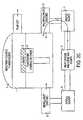
- FIG. 2Ais a graphical illustration of the operation of the FIG. 1 reaction vessel carrying out a first processing sequence.
- FIG. 2Bis a graphical illustration of purging the FIG. 1 chamber after the first processing sequence.
- FIG. 2Cis a graphical illustration of operating the FIG. 1 reaction vessel carrying out a second processing sequence.
- FIG. 2Dis a graphical illustration of purging the FIG. 1 chamber after the second processing sequence.
- FIG. 2Eis a cross-sectional view of the formation of a first nitride junction layer conducted in accordance with the present invention through methods depicted in FIGS. 2A-2D .
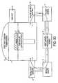
- FIG. 3Ais a graphical illustration of the first processing sequence in forming an intermediate junction layer.
- FIG. 3Bis a graphical illustration of purging the FIG. 3A chamber after the first processing sequence.
- FIG. 3Cis a graphical illustration of operating the FIG. 3B reaction vessel carrying out a second processing sequence.
- FIG. 3Dis a graphical illustration of purging the FIG. 3C chamber after the second processing sequence.
- FIG. 3Eis a cross-sectional view of the formation of the intermediate junction layer, formed over the first nitride junction layer, conducted in accordance with the processes depicted in FIGS. 3A-3D .
- FIG. 4is a cross-sectional view of the final reaction sequence used in formation of the second nitride junction layer conducted in accordance with the processes depicted in FIGS. 2A-2D .
- FIG. 5is a graphical illustration of plasma annealing the second nitride junction layer formed in accordance with the processes depicted in FIGS. 2A-2D .
- FIG. 6is a cross-sectional view of a magnetic tunnel junction barrier film constructed in accordance with the processes depicted in FIGS. 2A-2D .
- FIG. 7is a cross-sectional view of a magnetic tunnel junction barrier film and the formation of the intermediate junction layer constructed in accordance with the processes depicted in FIGS. 3A-3D .
- FIG. 8is a cross-sectional view of a magnetic tunnel junction barrier film and the formation of the second nitride junction layer constructed in accordance with the processes depicted in FIGS. 2A-2D .
- FIG. 9is a cross-sectional view of a multilayer magnetic tunnel junction barrier film constructed in accordance with the present invention.
- FIG. 10is a cross-sectional view of a magnetic tunnel junction device constructed in accordance with the present invention.
- FIG. 11is a block diagram of a system utilizing a magnetic tunnel junction device constructed in accordance with the present invention.
- the present inventionprovides a multilayer dielectric tunnel barrier used in magnetic tunnel junction devices and its method of fabrication.
- the multilayer filmhas lower barrier layer resistance, is very conformal, and can be made as a thicker or thinner film with fewer pinholes.
- the tunnel barrieris defined as the dielectric portion between two ferromagnetic layers.
- the electrical barrier heightmay be altered by changing the relative thicknesses of the nitride and oxide layers.
- the tunnel barrier thicknessis changed simply by the number of ALD deposition steps used in forming the alternating nitride and oxide layers.
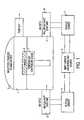
- FIG. 1is a graphical illustration of a reaction vessel 1 which can be employed for magnetic tunnel junction barrier film formation.
- a semiconductor wafer 2is disposed on a temperature controlled chuck 3 .
- Heated gas lines 9 and 10are utilized to introduce gases into the reaction vessel 1 during fabrication of the tunnel barrier layers.
- the temperature controlled chuck 3 temperaturecan range from approximately 25° C. to approximately 250° C.
- the semiconductor wafer 2has been previously processed to the point where a first ferromagnetic layer is provided on the exposed wafer surface.
- the inventionprovides a first nitride junction layer on the first ferromagnetic layer.
- the inventionwill be described below with use of AlN as comprising the first and second nitride junction layers.
- nitride layerssuch as Si x N y , TiN, HfN, TaN, and other alternative nitride layers known in the art, can also be used to form the first and second nitride junction layers.
- the reactant utilized in this inventionis described as NH 3 to form the first and second nitride junction layers, other reactants well-known in the art such as N 2 (plasma) or N from an atomic source (essentially a plasma that splits N 2 into N) can be utilized with equal effectiveness.
- TMAis the reactant utilized to form the first and second nitride junction layers
- other reactants well-known in the artsuch as Dimethyl Amine Alane (DMAA), Al(CH 3 ) 2 NH 2 can be used with equal effectiveness.
- DMAADimethyl Am
- the reaction vessel 1is first pumped down to a pressure at least less than 0.01 Torr i.e., a vacuum environment.
- Heated gas line 9allows an initial reactant such as Al(CH 3 ) 3 (TMA) 6 to enter reaction vessel 1 .
- Heated gas line 10allows a second reactant to enter reaction vessel 1 , such as water (H 2 O) 7 or ammonia (NH 3 ) 7 .
- either heated gas line 9 or 10may be utilized to send the initial reactant into the reaction vessel 1 .
- Gas lines 9 and 10are heated to a temperature of approximately 40° C. to approximately 120° C. depending upon the reactants utilized.
- heated gas line 10when carrying H 2 O 7 , should have a temperature at least greater than 100° C. to help avoid condensation of the reactant in heated gas line 10 .
- heated gas line 9when carrying TMA 6 , would only need to be heated from approximately 50° C. to approximately 60° C.
- O 3is used as a reactant
- the heated gas line utilizedwould not require a temperature above 50° C. In essence, the temperature of the heated gas line utilized, just needs to be high enough to avoid condensation of the reactants in the heated gas line.
- TMA 6from heated gas line 9 , or NH 3 7 from heated gas line 10 can be introduced as the first reactant into reaction vessel 1 .
- TMA 6is introduced as the initial reactant through heated gas line 9
- NH 3 7is then introduced as the second reactant through heated gas line 10 to form an AlN monolayer.
- TMA 6is then introduced as the second reactant through heated gas line 9 to form the AlN monolayer.
- alternating depositions of the first reactant and second reactantwill result in a nitride junction layer i.e., an AlN film, of a desired thickness.
- the inventionwill be described below with use of TMA 6 as the initial reactant. However, the invention is equally effective if NH 3 7 is used as the initial reactant.
- TMA 6is introduced at a rate of approximately 10 sccm to approximately 50 sccm through heated gas line 9 into the reaction vessel 1 .
- the TMA 6is transported to the semiconductor wafer surface 2 by an inert carrier gas 4 such as Ar (Argon).
- ArAr
- Wafer 2is dosed with a short pulse of TMA 6 to adsorb a continuous monolayer of TMA 6 on the wafer 2 surface.
- the reaction vessel 1is held at a pressure of approximately 0.1 Torr to approximately 200 Torr, for a period of approximately 1 second to approximately 10 seconds after deposition of Al as a monolayer from the TMA 6 reactant.
- a non-reactive gas 4such as Ar
- a non-reactive purge gasis passed through heated gas lines 9 and 10 to purge heated gas lines 9 and 10 and the reaction vessel 1 of residual reactant i.e., TMA 6 .
- Aris utilized as the non-reactive purge gas
- any non-reactive or inert gasmay be utilized as the purge gas with equal effectiveness.
- the non-reactive gas 4is introduced into the reaction vessel 1 through heated gas lines 9 and 10 at a rate of approximately 50 sccm.
- FIG. 2Billustrates a flow of purge gas through heated gas lines 9 and 10 which provides a quicker purge of the reaction vessel 1 and heated gas lines 9 and 10 , it is also possible to supply the non-reactive purge gas only through the heated gas line that supplied the initial reactant; here, in heated gas line 9 , in the process step shown in FIG. 2 A. Whereas if NH 3 7 is the initial reactant, the non-reactive purge gas 4 can be supplied through heated gas line 10 .
- FIG. 2Cgraphically illustrates that an inert carrier gas 4 such as Ar, is passed through heated gas line 10 carrying a second reactant i.e., NH 3 7 into reaction vessel 1 .
- a second reactanti.e., NH 3 7
- NH 3 7is introduced at a rate of approximately 10 sccm to approximately 50 sccm into reaction vessel 1 .
- the reaction vessel 1is held at a pressure of approximately 0.1 Torr to approximately 200 Torr, for a period of approximately 1 second to approximately 10 seconds during introduction of the second reactant into reaction vessel 1 .
- NH 3 7provides nitrogen atoms which are deposited as a monolayer on the wafer 2 and bonds with the Al atoms previously deposited from the first processing sequence; thus, providing a monolayer of AlN on the surface of wafer 2 .
- reaction vessel 1is purged again by passing a non-reactive gas 4 such as Ar, through heated gas lines 9 and 10 in order to purge heated gas lines 9 and 10 and reaction vessel 1 as shown in FIG. 2 D.
- the non-reactive gas 4is introduced at a rate of approximately 50 sccm. This step removes the reaction byproduct i.e., CH 4 and residual NH 3 7 , from reaction vessel 1 and heated gas lines 9 and 10 .
- FIG. 2Dillustrates the inert purge gas 4 passing through both heated gas lines 9 and 10 into reaction vessel 1 for a faster purge; it is also possible to just pass the inert purge gas 4 through the heated gas line that introduced the second reactant.
- FIG. 2Eis a cross-sectional view of the formation of the first nitride junction layer (AlN) on a first ferromagnetic layer after one cycle of the processing sequences depicted in FIGS. 2A-2D are carried out.
- TMAis not a stable compound and automatically reacts if exposed to the atmosphere. Thus, the processes depicted in FIGS. 2A-2D , must be carried out in a vacuum-like atmosphere to prevent TMA from prematurely reacting.
- TMA's volatilityis an additional reason that reaction vessel 1 and heated gas lines 9 and 10 must be purged prior to introducing a second reactant in the processing sequences depicted in FIGS. 2B and 2D .
- TMAis deposited on the first ferromagnetic layer (FIG. 2 E( 1 )) provided on the wafer 2 as depicted in FIG. 2 E( 2 ).
- TMAremains stable and non-volatile in reaction vessel's 1 vacuum-like environment and upon attachment goes to Al(CH 3 ) 2 .
- FIG. 2 E( 3 )which depicts the formation of AlNH 2 ; the introduction of the second reactant NH 3 , causes the methyl groups of TMA to disassociate from Al.
- Dimethyl Amine Alane (DMAA), Al(CH 3 ) 2 NH 2can also be used with equal effectiveness in forming the AlN part of the barrier.
- DMAADimethyl Amine Alane
- Al(CH 3 ) 2 NH 2can also be used with equal effectiveness in forming the AlN part of the barrier.
- reaction vessel 1 and heated gas lines 9 and 10are then purged as depicted in FIG. 2 D. This results in residual unreacted NH 3 and CH 4 byproducts to be expunged from reaction vessel 1 and the wafer 2 surface leaving a monolayer of AlNH 2 and AlNH to be reacted with another TMA molecule building Al—N—Al layers forming a pristine AlN film.
- the surface chemical reactions in forming an AlN monolayerare well-known in the art.
- FIGS. 2A-2Erespectively illustrates one continuous monolayer of reacted AlN deposited on wafer 2 after one cycle of the processing sequences depicted in FIGS. 2A-2D has been completed.
- the processing sequences depicted in FIGS. 2A-2Dcan be repeated to form additional monolayers of AlN to achieve the desired thickness of the first nitride junction layer i.e., AlN.
- a monolayer of AlN on the surfacewill have H or H 2 such as AlNH or AlNH 2 , but when reacted with another layer of TMA the monolayer of AlN goes to Al—N—Al as described previously.
- additional monolayers of AlNcan easily be fabricated according to the desired thickness.
- FIGS. 2A-2Dintroduces Al atoms first and then nitrogen atoms second in forming the AlN monolayer
- the processcan also be modified as noted above, to begin with a nitrogen atom layer and then an Al atom layer.
- NH 3 7is utilized as the initial reactant, depicted in FIG. 2C , in forming the first nitride junction layer (AlN).
- reaction vessel 1is purged as depicted in FIG. 2 D.
- TMA 6is introduced, as depicted in FIG. 2A , and then reaction vessel 1 is purged again as shown in FIG. 2B to complete one monolayer of AlN.
- the processing sequences, depicted in FIGS. 2A-2Dresults in an anatomically smooth monolayer of approximately 0.8 to approximately 1 Angstrom ( ⁇ ) of AlN deposited on the first ferromagnetic layer of wafer 2 .
- the process flow, depicted in FIGS. 2A-2Dcan be repeated any number of times as desired to fabricate additional monolayers of AlN on wafer 2 to achieve the desired thickness of the first nitride junction layer i.e., AlN.
- approximately 1 to approximately 68 monolayers of AlNis sufficient to protect the bottom ferromagnetic electrode and form the first nitride junction layer.
- the thickness of the first nitride junction layercan be tailored to provide the required magnetoresistance for any given device.
- the first AlN nitride junction layercan then be thermally annealed at a temperature of approximately 200° C. to approximately 250° C. This anneal occurs for a duration of approximately one minute to approximately ten minutes in a nitrogen (N 2 ) or oxygen (O 2 ) atmosphere. It is preferred that the first AlN nitride junction layer utilize a N 2 atmosphere in a thermal anneal to reduce the chance of oxidation at the first ferromagnetic film layer i.e., the initial ferromagnetic film provided on the semiconductor wafer. As a result of the thermal anneal, the level of impurities in the AlN a layer is decreased.
- the thermal annealing processreleases any unreacted reactants such as TMA 6 , releases the final CH 3 groups from the last layer of TMA 6 deposited, and drives out any trapped residual hydrogen in the film from NH 3 7 . Therefore, the process of thermally annealing the first AlN nitride junction layer aids in completion of nitride formation and reduces the hydrogen content of the film.
- an intermediate junction layeri.e., an oxide layer
- the intermediate junction layercan be comprised of A x O y , HfO, Ta 2 O 5 , SiO 2 , or combinations thereof and other materials well-known in the art.
- the intermediate junction layeri.e., an oxide layer, is described as an Al x O y layer.
- Either TMA 6 , from heated gas line 9 , or H 2 O 7 from heated gas line 10can be introduced as the first reactant into reaction vessel 1 .
- TMA 6is introduced as the first reactant through heated gas line 9
- H 2 O 7is then introduced as the second reactant through heated gas line 10 in forming the Al x O y layer.
- TMA 6is then introduced as the second reactant through heated gas line 9 to form an Al x O y intermediate junction layer.
- alternating depositions of the first reactant and second reactantwill result in an intermediate oxide junction layer i.e., an oxide layer (Al x O y ), of a desired thickness provided on the first nitride junction layer (AlN).
- the inventionwill be described below with use of TMA 6 as the initial reactant. However, the invention is equally effective if H 2 O 7 is used as the initial reactant. Furthermore, for purposes of simplification, the invention will be described below with use of H 2 O 7 as the second reactant in forming the Al x O y intermediate oxide junction layer. However, other reactants such as O 3 , H 2 0 2 , and other alternative reactants well-known in the art, can also be used as the second reactant in forming the Al x O y intermediate oxide junction layer with equal effectiveness.
- TMA 6is introduced as the first reactant through heated gas line 9 into reaction vessel 1 and transported to the semiconductor wafer 2 by an inert carrier gas 4 such as Ar.
- TMA 6is introduced at a rate of approximately 10 sccm to approximately 50 sccm as the first reactant through heated gas line 9 into reaction vessel 1 .
- Wafer 2is dosed with a short pulse of TMA 6 to adsorb a continuous monolayer of Al on the wafer 2 surface.
- the reaction vessel 1is held at a pressure of approximately 0.1 Torr to approximately 200 Torr, for a period of approximately 1 second to approximately 10 seconds during Al atom depositions.
- an inert gas 4i.e., Ar
- the non-reactive gas 4is introduced into reaction vessel 1 through heated gas lines 9 and 10 at a rate of approximately 50 sccm.
- FIG. 3Billustrates the inert purge gas 4 passing through both heated gas lines 9 and 10 into reaction vessel 1 for a faster purge, it is also possible to just pass the inert purge gas 4 through the heated gas line introducing the first reactant. If H 2 O 7 is the initial reactant and TMA 6 is the second reactant, the inert purge gas would then be applied through heated gas line 10 .
- an inert carrier gas 4i.e., Ar
- heated gas line 10carrying H 2 O 7 into reaction vessel 1 .
- H 2 O 7is introduced into reaction vessel 1 at a rate of approximately 10 sccm to approximately 50 sccm.
- Reaction vessel 1is held at a pressure of approximately 0.1 Torr to approximately 200 Torr, for a period of approximately 1 second to approximately 10 seconds during the introduction of H 2 O 7 .
- H 2 O 7provides oxygen atoms which are deposited as a monolayer on the wafer 2 and bonds with the Al atoms previously deposited from the first processing sequence; thus, providing a continuous monolayer of Al x O y on the first nitride junction layer provided on the wafer 2 surface.
- FIG. 3Dgraphically illustrates the introduction of an inert gas 4 i.e., Ar, through heated gas lines 9 and 10 , to purge heated gas lines 9 and 10 and reaction vessel 1 .
- the non-reactive gas 4enters reaction vessel 1 through heated gas lines 9 and 10 at a rate of approximately 50 sccm.
- the non-reactive gas 4serves to remove the reacted CH 4 and residual H 2 O 7 .
- the inert purge gas 4need only be supplied through heated gas line 10 if desired.
- FIG. 3Eis a cross-sectional view of the formation of the Al x O y intermediate oxide junction layer after one cycle of the processing sequences depicted in FIGS. 3A-3D are carried out.
- the introduction of H 2 O into reaction vessel 1produces an Al x O y monolayer by reacting with the TMA as depicted in FIG. 3 E( 4 ).
- the bond formation between the hydroxyl groups (OH) and Alis a far more stable bond (i.e., more energetically favorable) than the C and Al bond of TMA.
- H 2 Oencounters the Al—CH 3 bond and the Al—OH bond is energetically more favorable driving the disassociation reaction of the methyl groups from Al and OH groups from H.
- the Al—OH bondforms leaving CH 3 which disassociates and picks up the other hydrogen from the Al—OH reaction leaving CH 4 as the by-product as depicted in FIG. 3 E( 3 ).
- the second purgeas depicted in FIG. 3D , removes the reacted CH 4 and residual unreacted reactants from reaction vessel 1 , leaving a continuous monolayer of Al x O y (FIG. 3 E( 4 )).
- the surface chemical reactionsare well-known in the art.
- FIGS. 3A-3Erespectively illustrates one continuous monolayer of the Al x O y layer after one processing cycle has been completed.
- the processing sequences in FIGS. 3 A- 3 Dcan be repeated to fabricate additional monolayers to the Al x O y layer until a desired thickness is achieved.
- the embodiment of the invention illustrated in FIGS. 3A-3Ddeposits Al first, and then OH second to form an Al x O y monolayer
- the processcan also be modified to deposit OH first rather than second.
- H 2 O 7can be utilized as the initial reactant, as depicted in FIG. 3C , in forming the intermediate oxide junction layer (Al x O y ).
- reaction vessel 1is purged as depicted in FIG. 3 D.
- TMA 6is introduced, as depicted in FIG. 3A , and then reaction vessel 1 is purged, as shown in FIG. 3B , to complete one monolayer of Al x O y .
- the processing sequences depicted in FIGS. 3A-3Dresults in an anatomically smooth monolayer of approximately 0.8 to approximately 1 Angstrom ( ⁇ ) of Al x O y deposited on the first nitride junction layer 20 of wafer 2 (FIG. 3 E( 1 )).
- the process flow, depicted in FIGS. 3A-3Dcan be repeated any number of times as desired to fabricate additional monolayers of Al x O y provided on the first nitride junction layer 20 , to achieve the desired thickness of the intermediate oxide junction layer i.e., Al x O y .
- approximately 1 to approximately 68 monolayers of Alloyis sufficient to form the intermediate oxide junction layer.
- the total thickness of the Al x O y layeris approximately 0.8 ⁇ to approximately 58 ⁇ .
- the thickness of the Al x O y layercan be tailored to provide the required magnetoresistance for any given device.
- the completed Al x O y intermediate oxide junction layercan then be thermally annealed at a temperature of approximately 200° C. to approximately 250° C., for approximately one to approximately ten minutes, in a N 2 or O 2 atmosphere.
- an O 2 or N 2 plasmacan be utilized rather than a thermal anneal.
- the Al x O y intermediate oxide junction layeris thermally annealed in a N 2 atmosphere to reduce the chance of oxidation.
- the process step of thermally annealing the Al x O y intermediate oxide junction layeris to improve film density and reduce pinholing.
- the thermal annealreleases any unreacted reactants and drives out any trapped hydrogen; thereby, reducing the number of impurities present in the intermediate oxide junction layer.
- This processresults in a tunnel junction barrier that has two completed layers, the first nitride junction layer 20 and the intermediate oxide junction layer 30 depicted in FIG. 3 E( 4 ).
- the combined thickness of these layersare approximately 1.6 ⁇ to approximately 59 ⁇ .
- a second nitride junction layer 40is provided on top of the Al x O y intermediate oxide junction layer 30 .
- the inventionwill be described below with use of AlN as the second nitride junction layer 40 .
- similar nitride layerssuch as Si x N y , TiN, HfN, TaN, and other alternative nitride layers known in the art, can also be used to form the second nitride junction layer 40 .
- the second nitride junction layer 40is an AlN nitride junction layer provided on the intermediate oxide junction layer 30 described above.
- the AlN second nitride junction layer 40is formed utilizing the same processing sequences depicted in FIGS. 2A-2D , and as described in preceding paragraphs 42 to 55 prior to deposition of the top ferromagnetic layer.
- the thickness of the AlN second nitride junction layer 40can be tailored to any magnetoresistance that would be required for any given device.
- FIGS. 2C-2DAn additional embodiment of the present invention does not utilize the sequences depicted in FIGS. 2C-2D in completing formation of the second nitride junction layer 40 . It is preferred that the second nitride junction layer 40 react with NH 3 7 to avoid exposure to O 2 or other materials on its way to undergoing a plasma anneal.
- FIGS. 2A-2Ddepict processing sequences where Al atoms 6 are first deposited followed by N atom depositions 7 . However, the processes depicted in FIGS. 2C-2D involving N atoms depositions 7 in reaction vessel 1 can be eliminated by utilizing an alternative processing sequence.
- Al atoms 6are first deposited as depicted in FIGS. 2A-2B . These Al atoms 6 do not need to subsequently react with NH 3 7 to form the second nitride junction layer, as depicted in FIGS. 2C-2D , if an alternative processing sequence is used that ignites a N 2 plasma to densify the film such as a plasma anneal. This alternative processing step serves to provide the necessary N atoms in forming the second AlN nitride junction monolayer when the processing steps depicted in FIGS. 2C-2D are not utilized.
- the resulting second AlN nitride junction layer 40undergo a plasma anneal to improve the overall performance of the dielectric tunnel barrier.
- the plasma anneal processing stepis preferred whether FIGS. 2A-2D are utilized, or FIGS. 2A-2B are utilized in forming the second nitride AlN monolayer.
- the plasma anneal processing stepensures pinhole free dense tunnel barrier films, reduces impurities (unreacted reactants), and stabilizes the tunnel barrier film against high temperatures and humidity.
- FIG. 5graphically illustrates a plasma anneal process on the second AlN nitride junction layer after the desired thickness of the multilayer film has been achieved.
- the plasma densification processis not used on the first two layers (the first nitride junction layer and the intermediate oxide junction layer) of the dielectric tunnel barrier device in order to avoid damaging the bottom ferromagnetic layer.
- the first nitride junction layer and intermediate oxide junction layerundergo thermal anneals and do not require the step of plasma densification as the second nitride junction layer does.
- the plasma densification processconducted only on the second nitride junction layer, can be carried out in the reaction vessel 1 of FIG. 1 , as depicted in FIG. 5 , or in a separate chamber with an Rf, microwave plasma, or glow discharge source.
- the reaction vessel 1(or separate chamber) is backfilled with N 2 7 and the inductively coupled plasma source 5 , at the top of reaction vessel 1 is started.
- FIGS. 6-9are cross-sectional views of the different alternating layers of a tunnel barrier structure created by utilizing the processing sequences depicted in FIGS. 1-5 .
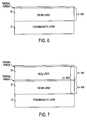
- FIG. 6is a cross-sectional view after the first nitride junction layer 20 i.e., AlN, is formed over the bottom ferromagnetic layer 10 and thermally annealed.
- FIG. 6depicts that the first nitride junction layer's 20 thickness can range from approximately 0.8 ⁇ to approximately 58 ⁇ .
- FIG. 7is a cross-sectional view after the intermediate oxide junction layer 30 i.e., Al x O y , is formed over the first nitride junction layer 20 and thermally annealed.
- FIG. 7depicts that the intermediate oxide junction layer 30 can range from approximately 0.8 ⁇ to approximately 58 ⁇ in thickness.
- FIG. 7also depicts that the combined thickness of the intermediate oxide junction layer 30 and the first nitride junction layer is approximately 1.6 ⁇ to approximately 59 ⁇ .
- FIG. 8is a cross-sectional view after the second nitride junction layer 40 i.e., AlN, which is provided on the intermediate oxide junction layer 30 , after undergoing a nitrogen plasma anneal process.
- FIG. 8depicts that the second nitride junction layer 40 can range from approximately 0.8 ⁇ , to approximately 58 ⁇ in thickness.
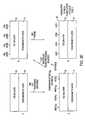
- FIG. 9is a cross-sectional view of a magnetic tunnel barrier device, constructed utilizing the methods of the present invention. As shown, a pair of ferromagnetic layers 10 and 50 , are separated by a multilayer tunnel junction barrier ( 20 , 30 , 40 ) constructed as described above.
- FIG. 9depicts that the completed multilayer tunnel junction barrier ( 20 , 30 , 40 ) can range from approximately 2.4 ⁇ to approximately 60 ⁇ in total thickness.
- FIG. 10is a cross-sectional view of a magnetic tunnel junction memory element suitable for use in an MRAM memory device utilizing the multilayer dielectric tunnel barrier ( 20 , 30 , 40 ) constructed in accordance with the present invention.
- the multilayer tunnel barrier ( 20 , 30 , 40 )interfaces with two ferromagnetic film layers ( 10 and 50 ), one of which is pinned and the other of which is free.
- alternating individual nitride-oxide-nitride layers ( 20 , 30 , 40 )each have a thickness of approximately 0.8 ⁇ to approximately 58 ⁇ , the overall thickness of the multilayer tunnel barrier ( 20 , 30 , 40 ) constructed in accordance with the present invention, does not exceed approximately 60 ⁇ .
- the multilayer tunnel barrier ( 20 , 30 , 40 )can be as thin as approximately 2.4 ⁇ thick.
- the top and bottom ferromagnetic layers ( 10 and 50 )may also interface with a capping 60 and seeding layer 0 respectively, depending on the device that will utilize the multilayer tunnel barrier ( 20 , 30 , 40 ).
- FIG. 11is a block diagram of a processor system utilizing the multilayer dielectric tunnel barrier structure as described above.
- the processor system 500may be a computer system comprising CPU 510 which exchanges data with an MRAM memory element 540 containing memory cells constructed as described above.
- the MRAM memory element 540communicates with CPU 510 over one or more buses and/or bridges 570 directly or through a memory controller.
- the buses and/or bridges 570also allow the CPU 510 to internally communicate with I/O devices 520 , 530 , read-only memory (ROM) devices 540 , and peripheral devices such as a floppy disk drive 550 and a compact disk CD-ROM drive 560 , as is well known in the art.
- ROMread-only memory
- the present inventionalso provides a magnetic memory device such as a storage cell which can be fabricated with a multilayer tunnel barrier that is comprised of only two monolayers of AlN and one monolayer of Al x O y , with a combined overall thickness of approximately 2.4 ⁇ to approximately 3 ⁇ .
- the multilayer tunnel barrier fabricated utilizing the methods described abovehas reduced pinholes, improves signal levels, improves overall device speed, and provides anatomically smooth surfaces.
- any combination of the thicknesses of the respective alternating layers of nitride i.e., AlN, and oxide i.e., Al x O ycan be used depending upon the device that will utilize the present invention.
- the only limiting factoris that the resulting tunnel barrier structure possess a minimum thickness of approximately 2.4 ⁇ and a maximum thickness of approximately 60 ⁇ .
- the present inventionis equally effective with alternating layers of nitride-oxide-nitride that are equal in thickness to each other.
- the tunnel barriercan be tuned (i.e., the magnetoresistance) by choosing the thicknesses of each alternating layer within a nitride or oxide layer or the nitride or oxide layer itself.
- Examples of using the present inventioninclude creation of a tunnel barrier that has a 4 ⁇ AlN layer (a first nitride junction layer), 4 ⁇ Al x O y layer (an intermediate oxide junction layer), and a 2 ⁇ AlN layer (a second nitride junction layer).
- a tunnel barrierhaving different layers of thickness such as: 6 ⁇ AlN, 10 ⁇ Al x O y , and 6 ⁇ AlN; a 20 ⁇ AlN, 5 ⁇ Al x O y , and 30 ⁇ AlN; 4 ⁇ AlN, 4 ⁇ Al x O y , and 4 ⁇ AlN; 2 ⁇ AlN, 6 ⁇ Al x O y , and 2 ⁇ AlN; 4 ⁇ AlN, 10 ⁇ Al x O y , and 4 ⁇ AlN; and 20 ⁇ AlN, 40 ⁇ Al x O y , and 20 ⁇ AlN for instance.
- the present inventionallows one to tune the resistance of any given magnetic device utilizing the multilayer tunnel barrier as described above.
- the present inventionalso provides a method and structure capable of simultaneously reducing the overall resistance of the tunnel barrier, and the occurrence of pinhole formation, while permitting films of various thickness to be formed.
- the dielectric tunnel barriers conformality and surface smoothness,is substantially enhanced compared to those dielectric tunnel barriers associated with conventional structures and methods.
- the ALD processleaves the interfaces of the tunnel barrier structure as pristine as possible by avoiding metal mixing and overoxidation from a plasma source. Furthermore, the ALD deposition techniques allows a multilayer tunnel barrier to be very thin improving signal levels and overall device speeds.
- the present inventionalso provides more precise stoichiometric control over the two nitride and oxide films and barrier height.
- the inventionhas been described and illustrated as being suitable for use in a memory application, an application for example, as in an MRAM device; the invention is not limited to MRAM applications. Rather, the invention and methods described in previous paragraphs, could be employed in any processor system in which an enhanced tunneling characteristic of a magnetic tunnel junction is desired.
Landscapes
- Chemical & Material Sciences (AREA)
- Engineering & Computer Science (AREA)
- Power Engineering (AREA)
- Materials Engineering (AREA)
- Manufacturing & Machinery (AREA)
- General Chemical & Material Sciences (AREA)
- Chemical Kinetics & Catalysis (AREA)
- Mechanical Engineering (AREA)
- Metallurgy (AREA)
- Organic Chemistry (AREA)
- Crystallography & Structural Chemistry (AREA)
- Nanotechnology (AREA)
- Inorganic Chemistry (AREA)
- Thermal Sciences (AREA)
- Physics & Mathematics (AREA)
- Hall/Mr Elements (AREA)
Abstract
Description
Claims (59)
Priority Applications (3)
| Application Number | Priority Date | Filing Date | Title |
|---|---|---|---|
| US10/165,301US6849464B2 (en) | 2002-06-10 | 2002-06-10 | Method of fabricating a multilayer dielectric tunnel barrier structure |
| US10/674,549US6900455B2 (en) | 2002-06-10 | 2003-10-01 | Multilayer dielectric tunnel barrier used in magnetic tunnel junction devices, and its method of fabrication |
| US11/106,509US7402833B2 (en) | 2002-06-10 | 2005-04-15 | Multilayer dielectric tunnel barrier used in magnetic tunnel junction devices, and its method of fabrication |
Applications Claiming Priority (1)
| Application Number | Priority Date | Filing Date | Title |
|---|---|---|---|
| US10/165,301US6849464B2 (en) | 2002-06-10 | 2002-06-10 | Method of fabricating a multilayer dielectric tunnel barrier structure |
Related Child Applications (1)
| Application Number | Title | Priority Date | Filing Date |
|---|---|---|---|
| US10/674,549DivisionUS6900455B2 (en) | 2002-06-10 | 2003-10-01 | Multilayer dielectric tunnel barrier used in magnetic tunnel junction devices, and its method of fabrication |
Publications (2)
| Publication Number | Publication Date |
|---|---|
| US20030228710A1 US20030228710A1 (en) | 2003-12-11 |
| US6849464B2true US6849464B2 (en) | 2005-02-01 |
Family
ID=29710409
Family Applications (3)
| Application Number | Title | Priority Date | Filing Date |
|---|---|---|---|
| US10/165,301Expired - LifetimeUS6849464B2 (en) | 2002-06-10 | 2002-06-10 | Method of fabricating a multilayer dielectric tunnel barrier structure |
| US10/674,549Expired - LifetimeUS6900455B2 (en) | 2002-06-10 | 2003-10-01 | Multilayer dielectric tunnel barrier used in magnetic tunnel junction devices, and its method of fabrication |
| US11/106,509Expired - LifetimeUS7402833B2 (en) | 2002-06-10 | 2005-04-15 | Multilayer dielectric tunnel barrier used in magnetic tunnel junction devices, and its method of fabrication |
Family Applications After (2)
| Application Number | Title | Priority Date | Filing Date |
|---|---|---|---|
| US10/674,549Expired - LifetimeUS6900455B2 (en) | 2002-06-10 | 2003-10-01 | Multilayer dielectric tunnel barrier used in magnetic tunnel junction devices, and its method of fabrication |
| US11/106,509Expired - LifetimeUS7402833B2 (en) | 2002-06-10 | 2005-04-15 | Multilayer dielectric tunnel barrier used in magnetic tunnel junction devices, and its method of fabrication |
Country Status (1)
| Country | Link |
|---|---|
| US (3) | US6849464B2 (en) |
Cited By (11)
| Publication number | Priority date | Publication date | Assignee | Title |
|---|---|---|---|---|
| US20050030786A1 (en)* | 2002-05-02 | 2005-02-10 | Micron Technology, Inc. | Low remanence flux concentrator for MRAM devices |
| US20050272272A1 (en)* | 2002-08-16 | 2005-12-08 | Samsung Electronics Co., Ltd. | Semiconductor device and method for manufacturing the same |
| US7002228B2 (en) | 2003-02-18 | 2006-02-21 | Micron Technology, Inc. | Diffusion barrier for improving the thermal stability of MRAM devices |
| US20060258090A1 (en)* | 2005-05-12 | 2006-11-16 | Micron Technology, Inc. | Band-engineered multi-gated non-volatile memory device with enhanced attributes |
| US20060284236A1 (en)* | 2005-06-21 | 2006-12-21 | Micron Technology, Inc. | Back-side trapped non-volatile memory device |
| US20070012988A1 (en)* | 2005-07-14 | 2007-01-18 | Micron Technology, Inc. | High density NAND non-volatile memory device |
| US20070045718A1 (en)* | 2005-08-31 | 2007-03-01 | Micron Technology, Inc. | Band engineered nano-crystal non-volatile memory device utilizing enhanced gate injection |
| US20070045711A1 (en)* | 2005-09-01 | 2007-03-01 | Micron Technology, Inc. | High performance multi-level non-volatile memory |
| US20070279977A1 (en)* | 2006-06-06 | 2007-12-06 | Micron Technology, Inc. | Semiconductor magnetic memory |
| CN102203971A (en)* | 2008-09-03 | 2011-09-28 | 佳能安内华股份有限公司 | Ferromagnetic preferential grain growth promoting seed layer for amorphous or microcrystalline MgO tunnel barrier |
| US20150214275A1 (en)* | 2014-01-24 | 2015-07-30 | National Taiwan University | Magnetic tunnel junction with superlattice barriers |
Families Citing this family (402)
| Publication number | Priority date | Publication date | Assignee | Title |
|---|---|---|---|---|
| US6972267B2 (en)* | 2002-03-04 | 2005-12-06 | Applied Materials, Inc. | Sequential deposition of tantalum nitride using a tantalum-containing precursor and a nitrogen-containing precursor |
| KR100469126B1 (en)* | 2002-06-05 | 2005-01-29 | 삼성전자주식회사 | Method of forming a thin film with a low hydrogen contents |
| US6849464B2 (en)* | 2002-06-10 | 2005-02-01 | Micron Technology, Inc. | Method of fabricating a multilayer dielectric tunnel barrier structure |
| KR100988081B1 (en)* | 2003-04-23 | 2010-10-18 | 삼성전자주식회사 | Magnetic ram having an intermediate oxide film formed in a heterogeneous method and a manufacturing method thereof |
| KR100521380B1 (en)* | 2003-05-29 | 2005-10-12 | 삼성전자주식회사 | Method of depositing a layer |
| US7057258B2 (en)* | 2003-10-29 | 2006-06-06 | Hewlett-Packard Development Company, L.P. | Resistive memory device and method for making the same |
| US7154779B2 (en)* | 2004-01-21 | 2006-12-26 | Sandisk Corporation | Non-volatile memory cell using high-k material inter-gate programming |
| JP2005302876A (en)* | 2004-04-08 | 2005-10-27 | Denso Corp | Tunnel magnetoresistive element, its manufacturing method and manufacturing equipment |
| WO2007033019A1 (en)* | 2005-09-12 | 2007-03-22 | Sandisk Corporation | Creating a dielectric layer using ald to deposit multiple components |
| US20070059945A1 (en)* | 2005-09-12 | 2007-03-15 | Nima Mohklesi | Atomic layer deposition with nitridation and oxidation |
| US7776763B2 (en)* | 2006-05-08 | 2010-08-17 | Tokyo Electron Limited | In-situ formation of oxidized aluminum nitride films |
| DE102007010286B4 (en)* | 2007-03-02 | 2013-09-05 | Freiberger Compound Materials Gmbh | A method for producing a compound semiconductor material, a III-N layer or a III-N bulk crystal, a reactor for producing the compound semiconductor material, compound semiconductor material, III-N bulk crystal and III-N crystal layer |
| EP2232576A2 (en)* | 2007-12-06 | 2010-09-29 | Craig Leidholm | Methods and devices for processing a precursor layer in a group via environment |
| US7816278B2 (en)* | 2008-03-28 | 2010-10-19 | Tokyo Electron Limited | In-situ hybrid deposition of high dielectric constant films using atomic layer deposition and chemical vapor deposition |
| US10378106B2 (en) | 2008-11-14 | 2019-08-13 | Asm Ip Holding B.V. | Method of forming insulation film by modified PEALD |
| US9394608B2 (en) | 2009-04-06 | 2016-07-19 | Asm America, Inc. | Semiconductor processing reactor and components thereof |
| US8802201B2 (en) | 2009-08-14 | 2014-08-12 | Asm America, Inc. | Systems and methods for thin-film deposition of metal oxides using excited nitrogen-oxygen species |
| US9312155B2 (en) | 2011-06-06 | 2016-04-12 | Asm Japan K.K. | High-throughput semiconductor-processing apparatus equipped with multiple dual-chamber modules |
| US10364496B2 (en) | 2011-06-27 | 2019-07-30 | Asm Ip Holding B.V. | Dual section module having shared and unshared mass flow controllers |
| US10854498B2 (en) | 2011-07-15 | 2020-12-01 | Asm Ip Holding B.V. | Wafer-supporting device and method for producing same |
| US20130023129A1 (en) | 2011-07-20 | 2013-01-24 | Asm America, Inc. | Pressure transmitter for a semiconductor processing environment |
| JP5789149B2 (en)* | 2011-07-21 | 2015-10-07 | Jswアフティ株式会社 | Atomic layer growth method and atomic layer growth apparatus |
| DE102011112897A1 (en)* | 2011-09-06 | 2013-03-07 | Sentech Instruments Gmbh | Apparatus and method for coating a substrate |
| CN102296278A (en)* | 2011-09-26 | 2011-12-28 | 中国科学院微电子研究所 | A kind of preparation method of aluminum nitride film |
| US9017481B1 (en) | 2011-10-28 | 2015-04-28 | Asm America, Inc. | Process feed management for semiconductor substrate processing |
| US9007818B2 (en) | 2012-03-22 | 2015-04-14 | Micron Technology, Inc. | Memory cells, semiconductor device structures, systems including such cells, and methods of fabrication |
| SG11201405417YA (en)* | 2012-03-23 | 2014-10-30 | Picosun Oy | Atomic layer deposition method and apparatuses |
| US8923038B2 (en) | 2012-06-19 | 2014-12-30 | Micron Technology, Inc. | Memory cells, semiconductor device structures, memory systems, and methods of fabrication |
| US9054030B2 (en) | 2012-06-19 | 2015-06-09 | Micron Technology, Inc. | Memory cells, semiconductor device structures, memory systems, and methods of fabrication |
| US9659799B2 (en) | 2012-08-28 | 2017-05-23 | Asm Ip Holding B.V. | Systems and methods for dynamic semiconductor process scheduling |
| US9021985B2 (en) | 2012-09-12 | 2015-05-05 | Asm Ip Holdings B.V. | Process gas management for an inductively-coupled plasma deposition reactor |
| US10714315B2 (en) | 2012-10-12 | 2020-07-14 | Asm Ip Holdings B.V. | Semiconductor reaction chamber showerhead |
| US9034491B2 (en)* | 2012-11-30 | 2015-05-19 | Seagate Technology Llc | Low resistance area magnetic stack |
| US20160376700A1 (en) | 2013-02-01 | 2016-12-29 | Asm Ip Holding B.V. | System for treatment of deposition reactor |
| US9484191B2 (en) | 2013-03-08 | 2016-11-01 | Asm Ip Holding B.V. | Pulsed remote plasma method and system |
| US9589770B2 (en) | 2013-03-08 | 2017-03-07 | Asm Ip Holding B.V. | Method and systems for in-situ formation of intermediate reactive species |
| US9379315B2 (en) | 2013-03-12 | 2016-06-28 | Micron Technology, Inc. | Memory cells, methods of fabrication, semiconductor device structures, and memory systems |
| US9368714B2 (en) | 2013-07-01 | 2016-06-14 | Micron Technology, Inc. | Memory cells, methods of operation and fabrication, semiconductor device structures, and memory systems |
| US9466787B2 (en) | 2013-07-23 | 2016-10-11 | Micron Technology, Inc. | Memory cells, methods of fabrication, semiconductor device structures, memory systems, and electronic systems |
| US9461242B2 (en) | 2013-09-13 | 2016-10-04 | Micron Technology, Inc. | Magnetic memory cells, methods of fabrication, semiconductor devices, memory systems, and electronic systems |
| US9608197B2 (en) | 2013-09-18 | 2017-03-28 | Micron Technology, Inc. | Memory cells, methods of fabrication, and semiconductor devices |
| US9240412B2 (en) | 2013-09-27 | 2016-01-19 | Asm Ip Holding B.V. | Semiconductor structure and device and methods of forming same using selective epitaxial process |
| US10683571B2 (en) | 2014-02-25 | 2020-06-16 | Asm Ip Holding B.V. | Gas supply manifold and method of supplying gases to chamber using same |
| US10454024B2 (en) | 2014-02-28 | 2019-10-22 | Micron Technology, Inc. | Memory cells, methods of fabrication, and memory devices |
| US10167557B2 (en) | 2014-03-18 | 2019-01-01 | Asm Ip Holding B.V. | Gas distribution system, reactor including the system, and methods of using the same |
| US11015245B2 (en) | 2014-03-19 | 2021-05-25 | Asm Ip Holding B.V. | Gas-phase reactor and system having exhaust plenum and components thereof |
| US9281466B2 (en) | 2014-04-09 | 2016-03-08 | Micron Technology, Inc. | Memory cells, semiconductor structures, semiconductor devices, and methods of fabrication |
| US9269888B2 (en) | 2014-04-18 | 2016-02-23 | Micron Technology, Inc. | Memory cells, methods of fabrication, and semiconductor devices |
| US10858737B2 (en) | 2014-07-28 | 2020-12-08 | Asm Ip Holding B.V. | Showerhead assembly and components thereof |
| US9890456B2 (en) | 2014-08-21 | 2018-02-13 | Asm Ip Holding B.V. | Method and system for in situ formation of gas-phase compounds |
| US10941490B2 (en) | 2014-10-07 | 2021-03-09 | Asm Ip Holding B.V. | Multiple temperature range susceptor, assembly, reactor and system including the susceptor, and methods of using the same |
| US9657845B2 (en) | 2014-10-07 | 2017-05-23 | Asm Ip Holding B.V. | Variable conductance gas distribution apparatus and method |
| US9349945B2 (en) | 2014-10-16 | 2016-05-24 | Micron Technology, Inc. | Memory cells, semiconductor devices, and methods of fabrication |
| KR102300403B1 (en) | 2014-11-19 | 2021-09-09 | 에이에스엠 아이피 홀딩 비.브이. | Method of depositing thin film |
| US9837281B2 (en) | 2014-11-26 | 2017-12-05 | Asm Ip Holding B.V. | Cyclic doped aluminum nitride deposition |
| US9799509B2 (en)* | 2014-11-26 | 2017-10-24 | Asm Ip Holding B.V. | Cyclic aluminum oxynitride deposition |
| US9768377B2 (en) | 2014-12-02 | 2017-09-19 | Micron Technology, Inc. | Magnetic cell structures, and methods of fabrication |
| KR102263121B1 (en) | 2014-12-22 | 2021-06-09 | 에이에스엠 아이피 홀딩 비.브이. | Semiconductor device and manufacuring method thereof |
| US10439131B2 (en)* | 2015-01-15 | 2019-10-08 | Micron Technology, Inc. | Methods of forming semiconductor devices including tunnel barrier materials |
| US10529542B2 (en) | 2015-03-11 | 2020-01-07 | Asm Ip Holdings B.V. | Cross-flow reactor and method |
| US10276355B2 (en) | 2015-03-12 | 2019-04-30 | Asm Ip Holding B.V. | Multi-zone reactor, system including the reactor, and method of using the same |
| US10458018B2 (en) | 2015-06-26 | 2019-10-29 | Asm Ip Holding B.V. | Structures including metal carbide material, devices including the structures, and methods of forming same |
| US10600673B2 (en) | 2015-07-07 | 2020-03-24 | Asm Ip Holding B.V. | Magnetic susceptor to baseplate seal |
| US10043661B2 (en) | 2015-07-13 | 2018-08-07 | Asm Ip Holding B.V. | Method for protecting layer by forming hydrocarbon-based extremely thin film |
| US10083836B2 (en) | 2015-07-24 | 2018-09-25 | Asm Ip Holding B.V. | Formation of boron-doped titanium metal films with high work function |
| US10745808B2 (en)* | 2015-07-24 | 2020-08-18 | Versum Materials Us, Llc | Methods for depositing Group 13 metal or metalloid nitride films |
| US9711345B2 (en)* | 2015-08-25 | 2017-07-18 | Asm Ip Holding B.V. | Method for forming aluminum nitride-based film by PEALD |
| US9960072B2 (en) | 2015-09-29 | 2018-05-01 | Asm Ip Holding B.V. | Variable adjustment for precise matching of multiple chamber cavity housings |
| US10211308B2 (en) | 2015-10-21 | 2019-02-19 | Asm Ip Holding B.V. | NbMC layers |
| US10322384B2 (en) | 2015-11-09 | 2019-06-18 | Asm Ip Holding B.V. | Counter flow mixer for process chamber |
| US11139308B2 (en) | 2015-12-29 | 2021-10-05 | Asm Ip Holding B.V. | Atomic layer deposition of III-V compounds to form V-NAND devices |
| US10468251B2 (en) | 2016-02-19 | 2019-11-05 | Asm Ip Holding B.V. | Method for forming spacers using silicon nitride film for spacer-defined multiple patterning |
| US10529554B2 (en) | 2016-02-19 | 2020-01-07 | Asm Ip Holding B.V. | Method for forming silicon nitride film selectively on sidewalls or flat surfaces of trenches |
| US10501866B2 (en) | 2016-03-09 | 2019-12-10 | Asm Ip Holding B.V. | Gas distribution apparatus for improved film uniformity in an epitaxial system |
| US10343920B2 (en) | 2016-03-18 | 2019-07-09 | Asm Ip Holding B.V. | Aligned carbon nanotubes |
| US9892913B2 (en) | 2016-03-24 | 2018-02-13 | Asm Ip Holding B.V. | Radial and thickness control via biased multi-port injection settings |
| US10087522B2 (en) | 2016-04-21 | 2018-10-02 | Asm Ip Holding B.V. | Deposition of metal borides |
| US10865475B2 (en) | 2016-04-21 | 2020-12-15 | Asm Ip Holding B.V. | Deposition of metal borides and silicides |
| US10190213B2 (en) | 2016-04-21 | 2019-01-29 | Asm Ip Holding B.V. | Deposition of metal borides |
| US10032628B2 (en) | 2016-05-02 | 2018-07-24 | Asm Ip Holding B.V. | Source/drain performance through conformal solid state doping |
| US10367080B2 (en) | 2016-05-02 | 2019-07-30 | Asm Ip Holding B.V. | Method of forming a germanium oxynitride film |
| KR102592471B1 (en) | 2016-05-17 | 2023-10-20 | 에이에스엠 아이피 홀딩 비.브이. | Method of forming metal interconnection and method of fabricating semiconductor device using the same |
| US11453943B2 (en) | 2016-05-25 | 2022-09-27 | Asm Ip Holding B.V. | Method for forming carbon-containing silicon/metal oxide or nitride film by ALD using silicon precursor and hydrocarbon precursor |
| US10388509B2 (en) | 2016-06-28 | 2019-08-20 | Asm Ip Holding B.V. | Formation of epitaxial layers via dislocation filtering |
| JP6823392B2 (en)* | 2016-07-05 | 2021-02-03 | 東京エレクトロン株式会社 | How to form an insulating film |
| US10612137B2 (en) | 2016-07-08 | 2020-04-07 | Asm Ip Holdings B.V. | Organic reactants for atomic layer deposition |
| US9859151B1 (en) | 2016-07-08 | 2018-01-02 | Asm Ip Holding B.V. | Selective film deposition method to form air gaps |
| US9793135B1 (en) | 2016-07-14 | 2017-10-17 | ASM IP Holding B.V | Method of cyclic dry etching using etchant film |
| US10714385B2 (en) | 2016-07-19 | 2020-07-14 | Asm Ip Holding B.V. | Selective deposition of tungsten |
| KR102354490B1 (en) | 2016-07-27 | 2022-01-21 | 에이에스엠 아이피 홀딩 비.브이. | Method of processing a substrate |
| US9812320B1 (en) | 2016-07-28 | 2017-11-07 | Asm Ip Holding B.V. | Method and apparatus for filling a gap |
| US10177025B2 (en) | 2016-07-28 | 2019-01-08 | Asm Ip Holding B.V. | Method and apparatus for filling a gap |
| US9887082B1 (en) | 2016-07-28 | 2018-02-06 | Asm Ip Holding B.V. | Method and apparatus for filling a gap |
| KR102532607B1 (en) | 2016-07-28 | 2023-05-15 | 에이에스엠 아이피 홀딩 비.브이. | Substrate processing apparatus and method of operating the same |
| US10395919B2 (en) | 2016-07-28 | 2019-08-27 | Asm Ip Holding B.V. | Method and apparatus for filling a gap |
| US10090316B2 (en) | 2016-09-01 | 2018-10-02 | Asm Ip Holding B.V. | 3D stacked multilayer semiconductor memory using doped select transistor channel |
| US10410943B2 (en) | 2016-10-13 | 2019-09-10 | Asm Ip Holding B.V. | Method for passivating a surface of a semiconductor and related systems |
| US10643826B2 (en) | 2016-10-26 | 2020-05-05 | Asm Ip Holdings B.V. | Methods for thermally calibrating reaction chambers |
| US11532757B2 (en) | 2016-10-27 | 2022-12-20 | Asm Ip Holding B.V. | Deposition of charge trapping layers |
| US10643904B2 (en) | 2016-11-01 | 2020-05-05 | Asm Ip Holdings B.V. | Methods for forming a semiconductor device and related semiconductor device structures |
| US10714350B2 (en) | 2016-11-01 | 2020-07-14 | ASM IP Holdings, B.V. | Methods for forming a transition metal niobium nitride film on a substrate by atomic layer deposition and related semiconductor device structures |
| US10435790B2 (en) | 2016-11-01 | 2019-10-08 | Asm Ip Holding B.V. | Method of subatmospheric plasma-enhanced ALD using capacitively coupled electrodes with narrow gap |
| US10229833B2 (en) | 2016-11-01 | 2019-03-12 | Asm Ip Holding B.V. | Methods for forming a transition metal nitride film on a substrate by atomic layer deposition and related semiconductor device structures |
| US10134757B2 (en) | 2016-11-07 | 2018-11-20 | Asm Ip Holding B.V. | Method of processing a substrate and a device manufactured by using the method |
| JP6253748B2 (en)* | 2016-11-09 | 2017-12-27 | 東京エレクトロン株式会社 | Film forming method and film forming apparatus |
| KR102546317B1 (en) | 2016-11-15 | 2023-06-21 | 에이에스엠 아이피 홀딩 비.브이. | Gas supply unit and substrate processing apparatus including the same |
| US10340135B2 (en) | 2016-11-28 | 2019-07-02 | Asm Ip Holding B.V. | Method of topologically restricted plasma-enhanced cyclic deposition of silicon or metal nitride |
| KR102762543B1 (en) | 2016-12-14 | 2025-02-05 | 에이에스엠 아이피 홀딩 비.브이. | Substrate processing apparatus |
| US11581186B2 (en) | 2016-12-15 | 2023-02-14 | Asm Ip Holding B.V. | Sequential infiltration synthesis apparatus |
| US11447861B2 (en) | 2016-12-15 | 2022-09-20 | Asm Ip Holding B.V. | Sequential infiltration synthesis apparatus and a method of forming a patterned structure |
| US9916980B1 (en) | 2016-12-15 | 2018-03-13 | Asm Ip Holding B.V. | Method of forming a structure on a substrate |
| KR102700194B1 (en) | 2016-12-19 | 2024-08-28 | 에이에스엠 아이피 홀딩 비.브이. | Substrate processing apparatus |
| US10269558B2 (en) | 2016-12-22 | 2019-04-23 | Asm Ip Holding B.V. | Method of forming a structure on a substrate |
| US10867788B2 (en) | 2016-12-28 | 2020-12-15 | Asm Ip Holding B.V. | Method of forming a structure on a substrate |
| US11390950B2 (en) | 2017-01-10 | 2022-07-19 | Asm Ip Holding B.V. | Reactor system and method to reduce residue buildup during a film deposition process |
| US10655221B2 (en) | 2017-02-09 | 2020-05-19 | Asm Ip Holding B.V. | Method for depositing oxide film by thermal ALD and PEALD |
| US10468261B2 (en) | 2017-02-15 | 2019-11-05 | Asm Ip Holding B.V. | Methods for forming a metallic film on a substrate by cyclical deposition and related semiconductor device structures |
| US10529563B2 (en) | 2017-03-29 | 2020-01-07 | Asm Ip Holdings B.V. | Method for forming doped metal oxide films on a substrate by cyclical deposition and related semiconductor device structures |
| US10283353B2 (en) | 2017-03-29 | 2019-05-07 | Asm Ip Holding B.V. | Method of reforming insulating film deposited on substrate with recess pattern |
| US10103040B1 (en) | 2017-03-31 | 2018-10-16 | Asm Ip Holding B.V. | Apparatus and method for manufacturing a semiconductor device |
| USD830981S1 (en) | 2017-04-07 | 2018-10-16 | Asm Ip Holding B.V. | Susceptor for semiconductor substrate processing apparatus |
| KR102457289B1 (en) | 2017-04-25 | 2022-10-21 | 에이에스엠 아이피 홀딩 비.브이. | Method for depositing a thin film and manufacturing a semiconductor device |
| US10446393B2 (en) | 2017-05-08 | 2019-10-15 | Asm Ip Holding B.V. | Methods for forming silicon-containing epitaxial layers and related semiconductor device structures |
| US10770286B2 (en) | 2017-05-08 | 2020-09-08 | Asm Ip Holdings B.V. | Methods for selectively forming a silicon nitride film on a substrate and related semiconductor device structures |
| US10892156B2 (en) | 2017-05-08 | 2021-01-12 | Asm Ip Holding B.V. | Methods for forming a silicon nitride film on a substrate and related semiconductor device structures |
| US10504742B2 (en) | 2017-05-31 | 2019-12-10 | Asm Ip Holding B.V. | Method of atomic layer etching using hydrogen plasma |
| US10886123B2 (en) | 2017-06-02 | 2021-01-05 | Asm Ip Holding B.V. | Methods for forming low temperature semiconductor layers and related semiconductor device structures |
| US12040200B2 (en) | 2017-06-20 | 2024-07-16 | Asm Ip Holding B.V. | Semiconductor processing apparatus and methods for calibrating a semiconductor processing apparatus |
| US11306395B2 (en) | 2017-06-28 | 2022-04-19 | Asm Ip Holding B.V. | Methods for depositing a transition metal nitride film on a substrate by atomic layer deposition and related deposition apparatus |
| US10685834B2 (en) | 2017-07-05 | 2020-06-16 | Asm Ip Holdings B.V. | Methods for forming a silicon germanium tin layer and related semiconductor device structures |
| KR20190009245A (en) | 2017-07-18 | 2019-01-28 | 에이에스엠 아이피 홀딩 비.브이. | Methods for forming a semiconductor device structure and related semiconductor device structures |
| US11018002B2 (en) | 2017-07-19 | 2021-05-25 | Asm Ip Holding B.V. | Method for selectively depositing a Group IV semiconductor and related semiconductor device structures |
| US10541333B2 (en) | 2017-07-19 | 2020-01-21 | Asm Ip Holding B.V. | Method for depositing a group IV semiconductor and related semiconductor device structures |
| US11374112B2 (en) | 2017-07-19 | 2022-06-28 | Asm Ip Holding B.V. | Method for depositing a group IV semiconductor and related semiconductor device structures |
| US10605530B2 (en) | 2017-07-26 | 2020-03-31 | Asm Ip Holding B.V. | Assembly of a liner and a flange for a vertical furnace as well as the liner and the vertical furnace |
| US10312055B2 (en) | 2017-07-26 | 2019-06-04 | Asm Ip Holding B.V. | Method of depositing film by PEALD using negative bias |
| US10590535B2 (en) | 2017-07-26 | 2020-03-17 | Asm Ip Holdings B.V. | Chemical treatment, deposition and/or infiltration apparatus and method for using the same |
| TWI815813B (en) | 2017-08-04 | 2023-09-21 | 荷蘭商Asm智慧財產控股公司 | Showerhead assembly for distributing a gas within a reaction chamber |
| US10692741B2 (en) | 2017-08-08 | 2020-06-23 | Asm Ip Holdings B.V. | Radiation shield |
| US10770336B2 (en) | 2017-08-08 | 2020-09-08 | Asm Ip Holding B.V. | Substrate lift mechanism and reactor including same |
| US11139191B2 (en) | 2017-08-09 | 2021-10-05 | Asm Ip Holding B.V. | Storage apparatus for storing cassettes for substrates and processing apparatus equipped therewith |
| US10249524B2 (en) | 2017-08-09 | 2019-04-02 | Asm Ip Holding B.V. | Cassette holder assembly for a substrate cassette and holding member for use in such assembly |
| US11769682B2 (en) | 2017-08-09 | 2023-09-26 | Asm Ip Holding B.V. | Storage apparatus for storing cassettes for substrates and processing apparatus equipped therewith |
| US10236177B1 (en) | 2017-08-22 | 2019-03-19 | ASM IP Holding B.V.. | Methods for depositing a doped germanium tin semiconductor and related semiconductor device structures |
| USD900036S1 (en) | 2017-08-24 | 2020-10-27 | Asm Ip Holding B.V. | Heater electrical connector and adapter |
| US11830730B2 (en) | 2017-08-29 | 2023-11-28 | Asm Ip Holding B.V. | Layer forming method and apparatus |
| US11295980B2 (en) | 2017-08-30 | 2022-04-05 | Asm Ip Holding B.V. | Methods for depositing a molybdenum metal film over a dielectric surface of a substrate by a cyclical deposition process and related semiconductor device structures |
| US11056344B2 (en) | 2017-08-30 | 2021-07-06 | Asm Ip Holding B.V. | Layer forming method |
| KR102491945B1 (en) | 2017-08-30 | 2023-01-26 | 에이에스엠 아이피 홀딩 비.브이. | Substrate processing apparatus |
| KR102401446B1 (en) | 2017-08-31 | 2022-05-24 | 에이에스엠 아이피 홀딩 비.브이. | Substrate processing apparatus |
| US10607895B2 (en) | 2017-09-18 | 2020-03-31 | Asm Ip Holdings B.V. | Method for forming a semiconductor device structure comprising a gate fill metal |
| KR102630301B1 (en) | 2017-09-21 | 2024-01-29 | 에이에스엠 아이피 홀딩 비.브이. | Method of sequential infiltration synthesis treatment of infiltrateable material and structures and devices formed using same |
| US10844484B2 (en) | 2017-09-22 | 2020-11-24 | Asm Ip Holding B.V. | Apparatus for dispensing a vapor phase reactant to a reaction chamber and related methods |
| US10658205B2 (en) | 2017-09-28 | 2020-05-19 | Asm Ip Holdings B.V. | Chemical dispensing apparatus and methods for dispensing a chemical to a reaction chamber |
| US10403504B2 (en) | 2017-10-05 | 2019-09-03 | Asm Ip Holding B.V. | Method for selectively depositing a metallic film on a substrate |
| US10319588B2 (en) | 2017-10-10 | 2019-06-11 | Asm Ip Holding B.V. | Method for depositing a metal chalcogenide on a substrate by cyclical deposition |
| US10923344B2 (en) | 2017-10-30 | 2021-02-16 | Asm Ip Holding B.V. | Methods for forming a semiconductor structure and related semiconductor structures |
| US10910262B2 (en) | 2017-11-16 | 2021-02-02 | Asm Ip Holding B.V. | Method of selectively depositing a capping layer structure on a semiconductor device structure |
| KR102443047B1 (en) | 2017-11-16 | 2022-09-14 | 에이에스엠 아이피 홀딩 비.브이. | Method of processing a substrate and a device manufactured by the same |
| US11022879B2 (en) | 2017-11-24 | 2021-06-01 | Asm Ip Holding B.V. | Method of forming an enhanced unexposed photoresist layer |
| CN111344522B (en) | 2017-11-27 | 2022-04-12 | 阿斯莫Ip控股公司 | Including clean mini-environment device |
| WO2019103613A1 (en) | 2017-11-27 | 2019-05-31 | Asm Ip Holding B.V. | A storage device for storing wafer cassettes for use with a batch furnace |
| US10290508B1 (en) | 2017-12-05 | 2019-05-14 | Asm Ip Holding B.V. | Method for forming vertical spacers for spacer-defined patterning |
| US10872771B2 (en) | 2018-01-16 | 2020-12-22 | Asm Ip Holding B. V. | Method for depositing a material film on a substrate within a reaction chamber by a cyclical deposition process and related device structures |
| KR102695659B1 (en) | 2018-01-19 | 2024-08-14 | 에이에스엠 아이피 홀딩 비.브이. | Method for depositing a gap filling layer by plasma assisted deposition |
| TWI799494B (en) | 2018-01-19 | 2023-04-21 | 荷蘭商Asm 智慧財產控股公司 | Deposition method |
| USD903477S1 (en) | 2018-01-24 | 2020-12-01 | Asm Ip Holdings B.V. | Metal clamp |
| US11018047B2 (en) | 2018-01-25 | 2021-05-25 | Asm Ip Holding B.V. | Hybrid lift pin |
| US10535516B2 (en) | 2018-02-01 | 2020-01-14 | Asm Ip Holdings B.V. | Method for depositing a semiconductor structure on a surface of a substrate and related semiconductor structures |
| USD880437S1 (en) | 2018-02-01 | 2020-04-07 | Asm Ip Holding B.V. | Gas supply plate for semiconductor manufacturing apparatus |
| US11081345B2 (en) | 2018-02-06 | 2021-08-03 | Asm Ip Holding B.V. | Method of post-deposition treatment for silicon oxide film |
| WO2019158960A1 (en) | 2018-02-14 | 2019-08-22 | Asm Ip Holding B.V. | A method for depositing a ruthenium-containing film on a substrate by a cyclical deposition process |
| US10896820B2 (en) | 2018-02-14 | 2021-01-19 | Asm Ip Holding B.V. | Method for depositing a ruthenium-containing film on a substrate by a cyclical deposition process |
| US10731249B2 (en) | 2018-02-15 | 2020-08-04 | Asm Ip Holding B.V. | Method of forming a transition metal containing film on a substrate by a cyclical deposition process, a method for supplying a transition metal halide compound to a reaction chamber, and related vapor deposition apparatus |
| US10658181B2 (en) | 2018-02-20 | 2020-05-19 | Asm Ip Holding B.V. | Method of spacer-defined direct patterning in semiconductor fabrication |
| KR102636427B1 (en) | 2018-02-20 | 2024-02-13 | 에이에스엠 아이피 홀딩 비.브이. | Substrate processing method and apparatus |
| US10975470B2 (en) | 2018-02-23 | 2021-04-13 | Asm Ip Holding B.V. | Apparatus for detecting or monitoring for a chemical precursor in a high temperature environment |
| US11473195B2 (en) | 2018-03-01 | 2022-10-18 | Asm Ip Holding B.V. | Semiconductor processing apparatus and a method for processing a substrate |
| US11629406B2 (en) | 2018-03-09 | 2023-04-18 | Asm Ip Holding B.V. | Semiconductor processing apparatus comprising one or more pyrometers for measuring a temperature of a substrate during transfer of the substrate |
| US11114283B2 (en) | 2018-03-16 | 2021-09-07 | Asm Ip Holding B.V. | Reactor, system including the reactor, and methods of manufacturing and using same |
| KR102646467B1 (en) | 2018-03-27 | 2024-03-11 | 에이에스엠 아이피 홀딩 비.브이. | Method of forming an electrode on a substrate and a semiconductor device structure including an electrode |
| US11088002B2 (en) | 2018-03-29 | 2021-08-10 | Asm Ip Holding B.V. | Substrate rack and a substrate processing system and method |
| US11230766B2 (en) | 2018-03-29 | 2022-01-25 | Asm Ip Holding B.V. | Substrate processing apparatus and method |
| US10510536B2 (en) | 2018-03-29 | 2019-12-17 | Asm Ip Holding B.V. | Method of depositing a co-doped polysilicon film on a surface of a substrate within a reaction chamber |
| KR102501472B1 (en) | 2018-03-30 | 2023-02-20 | 에이에스엠 아이피 홀딩 비.브이. | Substrate processing method |
| KR102600229B1 (en) | 2018-04-09 | 2023-11-10 | 에이에스엠 아이피 홀딩 비.브이. | Substrate supporting device, substrate processing apparatus including the same and substrate processing method |
| US12025484B2 (en) | 2018-05-08 | 2024-07-02 | Asm Ip Holding B.V. | Thin film forming method |
| TWI811348B (en) | 2018-05-08 | 2023-08-11 | 荷蘭商Asm 智慧財產控股公司 | Methods for depositing an oxide film on a substrate by a cyclical deposition process and related device structures |
| US12272527B2 (en) | 2018-05-09 | 2025-04-08 | Asm Ip Holding B.V. | Apparatus for use with hydrogen radicals and method of using same |
| KR20190129718A (en) | 2018-05-11 | 2019-11-20 | 에이에스엠 아이피 홀딩 비.브이. | Methods for forming a doped metal carbide film on a substrate and related semiconductor device structures |
| KR102596988B1 (en) | 2018-05-28 | 2023-10-31 | 에이에스엠 아이피 홀딩 비.브이. | Method of processing a substrate and a device manufactured by the same |
| US11718913B2 (en) | 2018-06-04 | 2023-08-08 | Asm Ip Holding B.V. | Gas distribution system and reactor system including same |
| TWI840362B (en) | 2018-06-04 | 2024-05-01 | 荷蘭商Asm Ip私人控股有限公司 | Wafer handling chamber with moisture reduction |
| US11286562B2 (en) | 2018-06-08 | 2022-03-29 | Asm Ip Holding B.V. | Gas-phase chemical reactor and method of using same |
| KR102568797B1 (en) | 2018-06-21 | 2023-08-21 | 에이에스엠 아이피 홀딩 비.브이. | Substrate processing system |
| US10797133B2 (en) | 2018-06-21 | 2020-10-06 | Asm Ip Holding B.V. | Method for depositing a phosphorus doped silicon arsenide film and related semiconductor device structures |
| TWI873894B (en) | 2018-06-27 | 2025-02-21 | 荷蘭商Asm Ip私人控股有限公司 | Cyclic deposition methods for forming metal-containing material and films and structures including the metal-containing material |
| KR102854019B1 (en) | 2018-06-27 | 2025-09-02 | 에이에스엠 아이피 홀딩 비.브이. | Periodic deposition method for forming a metal-containing material and films and structures comprising the metal-containing material |
| KR102686758B1 (en) | 2018-06-29 | 2024-07-18 | 에이에스엠 아이피 홀딩 비.브이. | Method for depositing a thin film and manufacturing a semiconductor device |
| US10612136B2 (en) | 2018-06-29 | 2020-04-07 | ASM IP Holding, B.V. | Temperature-controlled flange and reactor system including same |
| US10755922B2 (en) | 2018-07-03 | 2020-08-25 | Asm Ip Holding B.V. | Method for depositing silicon-free carbon-containing film as gap-fill layer by pulse plasma-assisted deposition |
| US10388513B1 (en) | 2018-07-03 | 2019-08-20 | Asm Ip Holding B.V. | Method for depositing silicon-free carbon-containing film as gap-fill layer by pulse plasma-assisted deposition |
| US10767789B2 (en) | 2018-07-16 | 2020-09-08 | Asm Ip Holding B.V. | Diaphragm valves, valve components, and methods for forming valve components |
| US10483099B1 (en) | 2018-07-26 | 2019-11-19 | Asm Ip Holding B.V. | Method for forming thermally stable organosilicon polymer film |
| US11053591B2 (en) | 2018-08-06 | 2021-07-06 | Asm Ip Holding B.V. | Multi-port gas injection system and reactor system including same |
| US10883175B2 (en) | 2018-08-09 | 2021-01-05 | Asm Ip Holding B.V. | Vertical furnace for processing substrates and a liner for use therein |
| US10829852B2 (en) | 2018-08-16 | 2020-11-10 | Asm Ip Holding B.V. | Gas distribution device for a wafer processing apparatus |
| US11430674B2 (en) | 2018-08-22 | 2022-08-30 | Asm Ip Holding B.V. | Sensor array, apparatus for dispensing a vapor phase reactant to a reaction chamber and related methods |
| KR102707956B1 (en) | 2018-09-11 | 2024-09-19 | 에이에스엠 아이피 홀딩 비.브이. | Method for deposition of a thin film |
| US11024523B2 (en) | 2018-09-11 | 2021-06-01 | Asm Ip Holding B.V. | Substrate processing apparatus and method |
| US11049751B2 (en) | 2018-09-14 | 2021-06-29 | Asm Ip Holding B.V. | Cassette supply system to store and handle cassettes and processing apparatus equipped therewith |
| CN110970344B (en) | 2018-10-01 | 2024-10-25 | Asmip控股有限公司 | Substrate holding apparatus, system comprising the same and method of using the same |
| US11232963B2 (en) | 2018-10-03 | 2022-01-25 | Asm Ip Holding B.V. | Substrate processing apparatus and method |
| KR102592699B1 (en) | 2018-10-08 | 2023-10-23 | 에이에스엠 아이피 홀딩 비.브이. | Substrate support unit and apparatuses for depositing thin film and processing the substrate including the same |
| US10847365B2 (en) | 2018-10-11 | 2020-11-24 | Asm Ip Holding B.V. | Method of forming conformal silicon carbide film by cyclic CVD |
| US10811256B2 (en) | 2018-10-16 | 2020-10-20 | Asm Ip Holding B.V. | Method for etching a carbon-containing feature |
| KR102605121B1 (en) | 2018-10-19 | 2023-11-23 | 에이에스엠 아이피 홀딩 비.브이. | Substrate processing apparatus and substrate processing method |
| KR102546322B1 (en) | 2018-10-19 | 2023-06-21 | 에이에스엠 아이피 홀딩 비.브이. | Substrate processing apparatus and substrate processing method |
| USD948463S1 (en) | 2018-10-24 | 2022-04-12 | Asm Ip Holding B.V. | Susceptor for semiconductor substrate supporting apparatus |
| US10381219B1 (en) | 2018-10-25 | 2019-08-13 | Asm Ip Holding B.V. | Methods for forming a silicon nitride film |
| US12378665B2 (en) | 2018-10-26 | 2025-08-05 | Asm Ip Holding B.V. | High temperature coatings for a preclean and etch apparatus and related methods |
| US11087997B2 (en) | 2018-10-31 | 2021-08-10 | Asm Ip Holding B.V. | Substrate processing apparatus for processing substrates |
| KR102748291B1 (en) | 2018-11-02 | 2024-12-31 | 에이에스엠 아이피 홀딩 비.브이. | Substrate support unit and substrate processing apparatus including the same |
| US11572620B2 (en) | 2018-11-06 | 2023-02-07 | Asm Ip Holding B.V. | Methods for selectively depositing an amorphous silicon film on a substrate |
| US11031242B2 (en) | 2018-11-07 | 2021-06-08 | Asm Ip Holding B.V. | Methods for depositing a boron doped silicon germanium film |
| US10818758B2 (en) | 2018-11-16 | 2020-10-27 | Asm Ip Holding B.V. | Methods for forming a metal silicate film on a substrate in a reaction chamber and related semiconductor device structures |
| US10847366B2 (en) | 2018-11-16 | 2020-11-24 | Asm Ip Holding B.V. | Methods for depositing a transition metal chalcogenide film on a substrate by a cyclical deposition process |
| US10559458B1 (en) | 2018-11-26 | 2020-02-11 | Asm Ip Holding B.V. | Method of forming oxynitride film |
| US12040199B2 (en) | 2018-11-28 | 2024-07-16 | Asm Ip Holding B.V. | Substrate processing apparatus for processing substrates |
| US11217444B2 (en) | 2018-11-30 | 2022-01-04 | Asm Ip Holding B.V. | Method for forming an ultraviolet radiation responsive metal oxide-containing film |
| KR102636428B1 (en) | 2018-12-04 | 2024-02-13 | 에이에스엠 아이피 홀딩 비.브이. | A method for cleaning a substrate processing apparatus |
| US11158513B2 (en) | 2018-12-13 | 2021-10-26 | Asm Ip Holding B.V. | Methods for forming a rhenium-containing film on a substrate by a cyclical deposition process and related semiconductor device structures |
| TWI874340B (en) | 2018-12-14 | 2025-03-01 | 荷蘭商Asm Ip私人控股有限公司 | Method of forming device structure, structure formed by the method and system for performing the method |
| TWI866480B (en) | 2019-01-17 | 2024-12-11 | 荷蘭商Asm Ip 私人控股有限公司 | Methods of forming a transition metal containing film on a substrate by a cyclical deposition process |
| KR102727227B1 (en) | 2019-01-22 | 2024-11-07 | 에이에스엠 아이피 홀딩 비.브이. | Semiconductor processing device |
| CN111524788B (en) | 2019-02-01 | 2023-11-24 | Asm Ip私人控股有限公司 | Method for forming topologically selective films of silicon oxide |
| TWI845607B (en) | 2019-02-20 | 2024-06-21 | 荷蘭商Asm Ip私人控股有限公司 | Cyclical deposition method and apparatus for filling a recess formed within a substrate surface |
| KR102626263B1 (en) | 2019-02-20 | 2024-01-16 | 에이에스엠 아이피 홀딩 비.브이. | Cyclical deposition method including treatment step and apparatus for same |
| TWI838458B (en) | 2019-02-20 | 2024-04-11 | 荷蘭商Asm Ip私人控股有限公司 | Apparatus and methods for plug fill deposition in 3-d nand applications |
| TWI873122B (en) | 2019-02-20 | 2025-02-21 | 荷蘭商Asm Ip私人控股有限公司 | Method of filling a recess formed within a surface of a substrate, semiconductor structure formed according to the method, and semiconductor processing apparatus |
| TWI842826B (en) | 2019-02-22 | 2024-05-21 | 荷蘭商Asm Ip私人控股有限公司 | Substrate processing apparatus and method for processing substrate |
| KR102782593B1 (en) | 2019-03-08 | 2025-03-14 | 에이에스엠 아이피 홀딩 비.브이. | Structure Including SiOC Layer and Method of Forming Same |
| KR102858005B1 (en) | 2019-03-08 | 2025-09-09 | 에이에스엠 아이피 홀딩 비.브이. | Method for Selective Deposition of Silicon Nitride Layer and Structure Including Selectively-Deposited Silicon Nitride Layer |
| US11742198B2 (en) | 2019-03-08 | 2023-08-29 | Asm Ip Holding B.V. | Structure including SiOCN layer and method of forming same |
| JP2020167398A (en) | 2019-03-28 | 2020-10-08 | エーエスエム・アイピー・ホールディング・ベー・フェー | Door openers and substrate processing equipment provided with door openers |
| KR102809999B1 (en) | 2019-04-01 | 2025-05-19 | 에이에스엠 아이피 홀딩 비.브이. | Method of manufacturing semiconductor device |
| KR20200123380A (en) | 2019-04-19 | 2020-10-29 | 에이에스엠 아이피 홀딩 비.브이. | Layer forming method and apparatus |
| KR20200125453A (en) | 2019-04-24 | 2020-11-04 | 에이에스엠 아이피 홀딩 비.브이. | Gas-phase reactor system and method of using same |
| US11289326B2 (en) | 2019-05-07 | 2022-03-29 | Asm Ip Holding B.V. | Method for reforming amorphous carbon polymer film |
| KR20200130121A (en) | 2019-05-07 | 2020-11-18 | 에이에스엠 아이피 홀딩 비.브이. | Chemical source vessel with dip tube |
| KR20200130652A (en) | 2019-05-10 | 2020-11-19 | 에이에스엠 아이피 홀딩 비.브이. | Method of depositing material onto a surface and structure formed according to the method |
| JP7612342B2 (en) | 2019-05-16 | 2025-01-14 | エーエスエム・アイピー・ホールディング・ベー・フェー | Wafer boat handling apparatus, vertical batch furnace and method |
| JP7598201B2 (en) | 2019-05-16 | 2024-12-11 | エーエスエム・アイピー・ホールディング・ベー・フェー | Wafer boat handling apparatus, vertical batch furnace and method |
| USD975665S1 (en) | 2019-05-17 | 2023-01-17 | Asm Ip Holding B.V. | Susceptor shaft |
| USD947913S1 (en) | 2019-05-17 | 2022-04-05 | Asm Ip Holding B.V. | Susceptor shaft |
| USD935572S1 (en) | 2019-05-24 | 2021-11-09 | Asm Ip Holding B.V. | Gas channel plate |
| USD922229S1 (en) | 2019-06-05 | 2021-06-15 | Asm Ip Holding B.V. | Device for controlling a temperature of a gas supply unit |
| KR20200141002A (en) | 2019-06-06 | 2020-12-17 | 에이에스엠 아이피 홀딩 비.브이. | Method of using a gas-phase reactor system including analyzing exhausted gas |
| KR20200141931A (en) | 2019-06-10 | 2020-12-21 | 에이에스엠 아이피 홀딩 비.브이. | Method for cleaning quartz epitaxial chambers |
| KR20200143254A (en) | 2019-06-11 | 2020-12-23 | 에이에스엠 아이피 홀딩 비.브이. | Method of forming an electronic structure using an reforming gas, system for performing the method, and structure formed using the method |
| USD944946S1 (en) | 2019-06-14 | 2022-03-01 | Asm Ip Holding B.V. | Shower plate |
| USD931978S1 (en) | 2019-06-27 | 2021-09-28 | Asm Ip Holding B.V. | Showerhead vacuum transport |
| KR20210005515A (en) | 2019-07-03 | 2021-01-14 | 에이에스엠 아이피 홀딩 비.브이. | Temperature control assembly for substrate processing apparatus and method of using same |
| JP7499079B2 (en) | 2019-07-09 | 2024-06-13 | エーエスエム・アイピー・ホールディング・ベー・フェー | Plasma device using coaxial waveguide and substrate processing method |
| CN112216646A (en) | 2019-07-10 | 2021-01-12 | Asm Ip私人控股有限公司 | Substrate supporting assembly and substrate processing device comprising same |
| KR20210010307A (en) | 2019-07-16 | 2021-01-27 | 에이에스엠 아이피 홀딩 비.브이. | Substrate processing apparatus |
| KR102860110B1 (en) | 2019-07-17 | 2025-09-16 | 에이에스엠 아이피 홀딩 비.브이. | Methods of forming silicon germanium structures |
| KR20210010816A (en) | 2019-07-17 | 2021-01-28 | 에이에스엠 아이피 홀딩 비.브이. | Radical assist ignition plasma system and method |
| US11643724B2 (en) | 2019-07-18 | 2023-05-09 | Asm Ip Holding B.V. | Method of forming structures using a neutral beam |
| KR20210010817A (en) | 2019-07-19 | 2021-01-28 | 에이에스엠 아이피 홀딩 비.브이. | Method of Forming Topology-Controlled Amorphous Carbon Polymer Film |
| TWI839544B (en) | 2019-07-19 | 2024-04-21 | 荷蘭商Asm Ip私人控股有限公司 | Method of forming topology-controlled amorphous carbon polymer film |
| TWI851767B (en) | 2019-07-29 | 2024-08-11 | 荷蘭商Asm Ip私人控股有限公司 | Methods for selective deposition utilizing n-type dopants and/or alternative dopants to achieve high dopant incorporation |
| CN112309900A (en) | 2019-07-30 | 2021-02-02 | Asm Ip私人控股有限公司 | Substrate processing apparatus |
| CN110459674B (en)* | 2019-07-30 | 2021-09-17 | 北京航空航天大学 | Magnetic tunnel junction, manufacturing method, spin diode and memory |
| US12169361B2 (en) | 2019-07-30 | 2024-12-17 | Asm Ip Holding B.V. | Substrate processing apparatus and method |
| CN112309899A (en) | 2019-07-30 | 2021-02-02 | Asm Ip私人控股有限公司 | Substrate processing apparatus |
| US11587814B2 (en) | 2019-07-31 | 2023-02-21 | Asm Ip Holding B.V. | Vertical batch furnace assembly |
| US11227782B2 (en) | 2019-07-31 | 2022-01-18 | Asm Ip Holding B.V. | Vertical batch furnace assembly |
| US11587815B2 (en) | 2019-07-31 | 2023-02-21 | Asm Ip Holding B.V. | Vertical batch furnace assembly |
| CN112323048B (en) | 2019-08-05 | 2024-02-09 | Asm Ip私人控股有限公司 | Liquid level sensor for chemical source container |
| CN112342526A (en) | 2019-08-09 | 2021-02-09 | Asm Ip私人控股有限公司 | Heater assembly including cooling device and method of using same |
| USD965524S1 (en) | 2019-08-19 | 2022-10-04 | Asm Ip Holding B.V. | Susceptor support |
| USD965044S1 (en) | 2019-08-19 | 2022-09-27 | Asm Ip Holding B.V. | Susceptor shaft |
| JP2021031769A (en) | 2019-08-21 | 2021-03-01 | エーエスエム アイピー ホールディング ビー.ブイ. | Production apparatus of mixed gas of film deposition raw material and film deposition apparatus |
| KR20210024423A (en) | 2019-08-22 | 2021-03-05 | 에이에스엠 아이피 홀딩 비.브이. | Method for forming a structure with a hole |
| USD940837S1 (en) | 2019-08-22 | 2022-01-11 | Asm Ip Holding B.V. | Electrode |
| USD930782S1 (en) | 2019-08-22 | 2021-09-14 | Asm Ip Holding B.V. | Gas distributor |
| USD949319S1 (en) | 2019-08-22 | 2022-04-19 | Asm Ip Holding B.V. | Exhaust duct |
| USD979506S1 (en) | 2019-08-22 | 2023-02-28 | Asm Ip Holding B.V. | Insulator |
| US11286558B2 (en) | 2019-08-23 | 2022-03-29 | Asm Ip Holding B.V. | Methods for depositing a molybdenum nitride film on a surface of a substrate by a cyclical deposition process and related semiconductor device structures including a molybdenum nitride film |
| KR20210024420A (en) | 2019-08-23 | 2021-03-05 | 에이에스엠 아이피 홀딩 비.브이. | Method for depositing silicon oxide film having improved quality by peald using bis(diethylamino)silane |
| KR102806450B1 (en) | 2019-09-04 | 2025-05-12 | 에이에스엠 아이피 홀딩 비.브이. | Methods for selective deposition using a sacrificial capping layer |
| KR102733104B1 (en) | 2019-09-05 | 2024-11-22 | 에이에스엠 아이피 홀딩 비.브이. | Substrate processing apparatus |
| US11562901B2 (en) | 2019-09-25 | 2023-01-24 | Asm Ip Holding B.V. | Substrate processing method |
| CN112593212B (en) | 2019-10-02 | 2023-12-22 | Asm Ip私人控股有限公司 | Method for forming topologically selective silicon oxide film by cyclic plasma enhanced deposition process |
| TWI846953B (en) | 2019-10-08 | 2024-07-01 | 荷蘭商Asm Ip私人控股有限公司 | Substrate processing device |
| KR20210042810A (en) | 2019-10-08 | 2021-04-20 | 에이에스엠 아이피 홀딩 비.브이. | Reactor system including a gas distribution assembly for use with activated species and method of using same |
| TW202128273A (en) | 2019-10-08 | 2021-08-01 | 荷蘭商Asm Ip私人控股有限公司 | Gas injection system, reactor system, and method of depositing material on surface of substratewithin reaction chamber |
| TWI846966B (en) | 2019-10-10 | 2024-07-01 | 荷蘭商Asm Ip私人控股有限公司 | Method of forming a photoresist underlayer and structure including same |
| US12009241B2 (en) | 2019-10-14 | 2024-06-11 | Asm Ip Holding B.V. | Vertical batch furnace assembly with detector to detect cassette |
| TWI834919B (en) | 2019-10-16 | 2024-03-11 | 荷蘭商Asm Ip私人控股有限公司 | Method of topology-selective film formation of silicon oxide |
| US11637014B2 (en) | 2019-10-17 | 2023-04-25 | Asm Ip Holding B.V. | Methods for selective deposition of doped semiconductor material |
| KR102845724B1 (en) | 2019-10-21 | 2025-08-13 | 에이에스엠 아이피 홀딩 비.브이. | Apparatus and methods for selectively etching films |
| KR20210050453A (en) | 2019-10-25 | 2021-05-07 | 에이에스엠 아이피 홀딩 비.브이. | Methods for filling a gap feature on a substrate surface and related semiconductor structures |
| US11646205B2 (en) | 2019-10-29 | 2023-05-09 | Asm Ip Holding B.V. | Methods of selectively forming n-type doped material on a surface, systems for selectively forming n-type doped material, and structures formed using same |
| KR20210054983A (en) | 2019-11-05 | 2021-05-14 | 에이에스엠 아이피 홀딩 비.브이. | Structures with doped semiconductor layers and methods and systems for forming same |
| US11501968B2 (en) | 2019-11-15 | 2022-11-15 | Asm Ip Holding B.V. | Method for providing a semiconductor device with silicon filled gaps |
| KR102861314B1 (en) | 2019-11-20 | 2025-09-17 | 에이에스엠 아이피 홀딩 비.브이. | Method of depositing carbon-containing material on a surface of a substrate, structure formed using the method, and system for forming the structure |
| CN112951697B (en) | 2019-11-26 | 2025-07-29 | Asmip私人控股有限公司 | Substrate processing apparatus |
| US11450529B2 (en) | 2019-11-26 | 2022-09-20 | Asm Ip Holding B.V. | Methods for selectively forming a target film on a substrate comprising a first dielectric surface and a second metallic surface |
| CN120432376A (en) | 2019-11-29 | 2025-08-05 | Asm Ip私人控股有限公司 | Substrate processing apparatus |
| CN112885692B (en) | 2019-11-29 | 2025-08-15 | Asmip私人控股有限公司 | Substrate processing apparatus |
| JP7527928B2 (en) | 2019-12-02 | 2024-08-05 | エーエスエム・アイピー・ホールディング・ベー・フェー | Substrate processing apparatus and substrate processing method |
| KR20210070898A (en) | 2019-12-04 | 2021-06-15 | 에이에스엠 아이피 홀딩 비.브이. | Substrate processing apparatus |
| KR20210078405A (en) | 2019-12-17 | 2021-06-28 | 에이에스엠 아이피 홀딩 비.브이. | Method of forming vanadium nitride layer and structure including the vanadium nitride layer |
| KR20210080214A (en) | 2019-12-19 | 2021-06-30 | 에이에스엠 아이피 홀딩 비.브이. | Methods for filling a gap feature on a substrate and related semiconductor structures |
| JP7636892B2 (en) | 2020-01-06 | 2025-02-27 | エーエスエム・アイピー・ホールディング・ベー・フェー | Channeled Lift Pins |
| JP7730637B2 (en) | 2020-01-06 | 2025-08-28 | エーエスエム・アイピー・ホールディング・ベー・フェー | Gas delivery assembly, components thereof, and reactor system including same |
| US11993847B2 (en) | 2020-01-08 | 2024-05-28 | Asm Ip Holding B.V. | Injector |
| KR20210093163A (en) | 2020-01-16 | 2021-07-27 | 에이에스엠 아이피 홀딩 비.브이. | Method of forming high aspect ratio features |
| KR102675856B1 (en) | 2020-01-20 | 2024-06-17 | 에이에스엠 아이피 홀딩 비.브이. | Method of forming thin film and method of modifying surface of thin film |
| TWI889744B (en) | 2020-01-29 | 2025-07-11 | 荷蘭商Asm Ip私人控股有限公司 | Contaminant trap system, and baffle plate stack |
| TW202513845A (en) | 2020-02-03 | 2025-04-01 | 荷蘭商Asm Ip私人控股有限公司 | Semiconductor structures and methods for forming the same |
| KR20210100010A (en) | 2020-02-04 | 2021-08-13 | 에이에스엠 아이피 홀딩 비.브이. | Method and apparatus for transmittance measurements of large articles |
| US11776846B2 (en) | 2020-02-07 | 2023-10-03 | Asm Ip Holding B.V. | Methods for depositing gap filling fluids and related systems and devices |
| KR20210103956A (en) | 2020-02-13 | 2021-08-24 | 에이에스엠 아이피 홀딩 비.브이. | Substrate processing apparatus including light receiving device and calibration method of light receiving device |
| TW202146691A (en) | 2020-02-13 | 2021-12-16 | 荷蘭商Asm Ip私人控股有限公司 | Gas distribution assembly, shower plate assembly, and method of adjusting conductance of gas to reaction chamber |
| TWI855223B (en) | 2020-02-17 | 2024-09-11 | 荷蘭商Asm Ip私人控股有限公司 | Method for growing phosphorous-doped silicon layer |
| CN113410160A (en) | 2020-02-28 | 2021-09-17 | Asm Ip私人控股有限公司 | System specially used for cleaning parts |
| KR20210113043A (en) | 2020-03-04 | 2021-09-15 | 에이에스엠 아이피 홀딩 비.브이. | Alignment fixture for a reactor system |
| US11876356B2 (en) | 2020-03-11 | 2024-01-16 | Asm Ip Holding B.V. | Lockout tagout assembly and system and method of using same |
| KR20210116240A (en) | 2020-03-11 | 2021-09-27 | 에이에스엠 아이피 홀딩 비.브이. | Substrate handling device with adjustable joints |
| KR102775390B1 (en) | 2020-03-12 | 2025-02-28 | 에이에스엠 아이피 홀딩 비.브이. | Method for Fabricating Layer Structure Having Target Topological Profile |
| US12173404B2 (en) | 2020-03-17 | 2024-12-24 | Asm Ip Holding B.V. | Method of depositing epitaxial material, structure formed using the method, and system for performing the method |
| KR102755229B1 (en) | 2020-04-02 | 2025-01-14 | 에이에스엠 아이피 홀딩 비.브이. | Thin film forming method |
| TWI887376B (en) | 2020-04-03 | 2025-06-21 | 荷蘭商Asm Ip私人控股有限公司 | Method for manufacturing semiconductor device |
| TWI888525B (en) | 2020-04-08 | 2025-07-01 | 荷蘭商Asm Ip私人控股有限公司 | Apparatus and methods for selectively etching silcon oxide films |
| KR20210128343A (en) | 2020-04-15 | 2021-10-26 | 에이에스엠 아이피 홀딩 비.브이. | Method of forming chromium nitride layer and structure including the chromium nitride layer |
| US11821078B2 (en) | 2020-04-15 | 2023-11-21 | Asm Ip Holding B.V. | Method for forming precoat film and method for forming silicon-containing film |
| US11996289B2 (en) | 2020-04-16 | 2024-05-28 | Asm Ip Holding B.V. | Methods of forming structures including silicon germanium and silicon layers, devices formed using the methods, and systems for performing the methods |
| KR20210130646A (en) | 2020-04-21 | 2021-11-01 | 에이에스엠 아이피 홀딩 비.브이. | Method for processing a substrate |
| KR20210132612A (en) | 2020-04-24 | 2021-11-04 | 에이에스엠 아이피 홀딩 비.브이. | Methods and apparatus for stabilizing vanadium compounds |
| TW202208671A (en) | 2020-04-24 | 2022-03-01 | 荷蘭商Asm Ip私人控股有限公司 | Methods of forming structures including vanadium boride and vanadium phosphide layers |
| KR102866804B1 (en) | 2020-04-24 | 2025-09-30 | 에이에스엠 아이피 홀딩 비.브이. | Vertical batch furnace assembly comprising a cooling gas supply |
| KR20210132600A (en) | 2020-04-24 | 2021-11-04 | 에이에스엠 아이피 홀딩 비.브이. | Methods and systems for depositing a layer comprising vanadium, nitrogen, and a further element |
| CN113555279A (en) | 2020-04-24 | 2021-10-26 | Asm Ip私人控股有限公司 | Methods of forming vanadium nitride-containing layers and structures comprising the same |
| KR102783898B1 (en) | 2020-04-29 | 2025-03-18 | 에이에스엠 아이피 홀딩 비.브이. | Solid source precursor vessel |
| KR20210134869A (en) | 2020-05-01 | 2021-11-11 | 에이에스엠 아이피 홀딩 비.브이. | Fast FOUP swapping with a FOUP handler |
| JP7726664B2 (en) | 2020-05-04 | 2025-08-20 | エーエスエム・アイピー・ホールディング・ベー・フェー | Substrate processing system for processing a substrate |
| KR102788543B1 (en) | 2020-05-13 | 2025-03-27 | 에이에스엠 아이피 홀딩 비.브이. | Laser alignment fixture for a reactor system |
| TW202146699A (en) | 2020-05-15 | 2021-12-16 | 荷蘭商Asm Ip私人控股有限公司 | Method of forming a silicon germanium layer, semiconductor structure, semiconductor device, method of forming a deposition layer, and deposition system |
| KR20210143653A (en) | 2020-05-19 | 2021-11-29 | 에이에스엠 아이피 홀딩 비.브이. | Substrate processing apparatus |
| KR20210145079A (en) | 2020-05-21 | 2021-12-01 | 에이에스엠 아이피 홀딩 비.브이. | Flange and apparatus for processing substrates |
| KR102795476B1 (en) | 2020-05-21 | 2025-04-11 | 에이에스엠 아이피 홀딩 비.브이. | Structures including multiple carbon layers and methods of forming and using same |
| TWI873343B (en) | 2020-05-22 | 2025-02-21 | 荷蘭商Asm Ip私人控股有限公司 | Reaction system for forming thin film on substrate |
| KR20210146802A (en) | 2020-05-26 | 2021-12-06 | 에이에스엠 아이피 홀딩 비.브이. | Method for depositing boron and gallium containing silicon germanium layers |
| TWI876048B (en) | 2020-05-29 | 2025-03-11 | 荷蘭商Asm Ip私人控股有限公司 | Substrate processing device |
| TW202212620A (en) | 2020-06-02 | 2022-04-01 | 荷蘭商Asm Ip私人控股有限公司 | Apparatus for processing substrate, method of forming film, and method of controlling apparatus for processing substrate |
| TW202208659A (en) | 2020-06-16 | 2022-03-01 | 荷蘭商Asm Ip私人控股有限公司 | Method for depositing boron containing silicon germanium layers |
| TW202218133A (en) | 2020-06-24 | 2022-05-01 | 荷蘭商Asm Ip私人控股有限公司 | Method for forming a layer provided with silicon |
| TWI873359B (en) | 2020-06-30 | 2025-02-21 | 荷蘭商Asm Ip私人控股有限公司 | Substrate processing method |
| US12431354B2 (en) | 2020-07-01 | 2025-09-30 | Asm Ip Holding B.V. | Silicon nitride and silicon oxide deposition methods using fluorine inhibitor |
| TW202202649A (en) | 2020-07-08 | 2022-01-16 | 荷蘭商Asm Ip私人控股有限公司 | Substrate processing method |
| KR20220010438A (en) | 2020-07-17 | 2022-01-25 | 에이에스엠 아이피 홀딩 비.브이. | Structures and methods for use in photolithography |
| KR20220011092A (en) | 2020-07-20 | 2022-01-27 | 에이에스엠 아이피 홀딩 비.브이. | Method and system for forming structures including transition metal layers |
| TWI878570B (en) | 2020-07-20 | 2025-04-01 | 荷蘭商Asm Ip私人控股有限公司 | Method and system for depositing molybdenum layers |
| US12322591B2 (en) | 2020-07-27 | 2025-06-03 | Asm Ip Holding B.V. | Thin film deposition process |
| KR20220021863A (en) | 2020-08-14 | 2022-02-22 | 에이에스엠 아이피 홀딩 비.브이. | Method for processing a substrate |
| US12040177B2 (en) | 2020-08-18 | 2024-07-16 | Asm Ip Holding B.V. | Methods for forming a laminate film by cyclical plasma-enhanced deposition processes |
| TW202228863A (en) | 2020-08-25 | 2022-08-01 | 荷蘭商Asm Ip私人控股有限公司 | Method for cleaning a substrate, method for selectively depositing, and reaction system |
| US11725280B2 (en) | 2020-08-26 | 2023-08-15 | Asm Ip Holding B.V. | Method for forming metal silicon oxide and metal silicon oxynitride layers |
| TW202229601A (en) | 2020-08-27 | 2022-08-01 | 荷蘭商Asm Ip私人控股有限公司 | Method of forming patterned structures, method of manipulating mechanical property, device structure, and substrate processing system |
| TW202217045A (en) | 2020-09-10 | 2022-05-01 | 荷蘭商Asm Ip私人控股有限公司 | Methods for depositing gap filing fluids and related systems and devices |
| USD990534S1 (en) | 2020-09-11 | 2023-06-27 | Asm Ip Holding B.V. | Weighted lift pin |
| KR20220036866A (en) | 2020-09-16 | 2022-03-23 | 에이에스엠 아이피 홀딩 비.브이. | Silicon oxide deposition method |
| USD1012873S1 (en) | 2020-09-24 | 2024-01-30 | Asm Ip Holding B.V. | Electrode for semiconductor processing apparatus |
| TWI889903B (en) | 2020-09-25 | 2025-07-11 | 荷蘭商Asm Ip私人控股有限公司 | Semiconductor processing method |
| US12009224B2 (en) | 2020-09-29 | 2024-06-11 | Asm Ip Holding B.V. | Apparatus and method for etching metal nitrides |
| KR20220045900A (en) | 2020-10-06 | 2022-04-13 | 에이에스엠 아이피 홀딩 비.브이. | Deposition method and an apparatus for depositing a silicon-containing material |
| CN114293174A (en) | 2020-10-07 | 2022-04-08 | Asm Ip私人控股有限公司 | Gas supply unit and substrate processing apparatus including the same |
| TW202229613A (en) | 2020-10-14 | 2022-08-01 | 荷蘭商Asm Ip私人控股有限公司 | Method of depositing material on stepped structure |
| TW202232565A (en) | 2020-10-15 | 2022-08-16 | 荷蘭商Asm Ip私人控股有限公司 | Method of manufacturing semiconductor device, and substrate treatment apparatus using ether-cat |
| TW202217037A (en) | 2020-10-22 | 2022-05-01 | 荷蘭商Asm Ip私人控股有限公司 | Method of depositing vanadium metal, structure, device and a deposition assembly |
| TW202223136A (en) | 2020-10-28 | 2022-06-16 | 荷蘭商Asm Ip私人控股有限公司 | Method for forming layer on substrate, and semiconductor processing system |
| TW202229620A (en) | 2020-11-12 | 2022-08-01 | 特文特大學 | Deposition system, method for controlling reaction condition, method for depositing |
| TW202229795A (en) | 2020-11-23 | 2022-08-01 | 荷蘭商Asm Ip私人控股有限公司 | A substrate processing apparatus with an injector |
| TW202235649A (en) | 2020-11-24 | 2022-09-16 | 荷蘭商Asm Ip私人控股有限公司 | Methods for filling a gap and related systems and devices |
| TW202235675A (en) | 2020-11-30 | 2022-09-16 | 荷蘭商Asm Ip私人控股有限公司 | Injector, and substrate processing apparatus |
| US12255053B2 (en) | 2020-12-10 | 2025-03-18 | Asm Ip Holding B.V. | Methods and systems for depositing a layer |
| TW202233884A (en) | 2020-12-14 | 2022-09-01 | 荷蘭商Asm Ip私人控股有限公司 | Method of forming structures for threshold voltage control |
| US11946137B2 (en) | 2020-12-16 | 2024-04-02 | Asm Ip Holding B.V. | Runout and wobble measurement fixtures |
| TW202232639A (en) | 2020-12-18 | 2022-08-16 | 荷蘭商Asm Ip私人控股有限公司 | Wafer processing apparatus with a rotatable table |
| TW202231903A (en) | 2020-12-22 | 2022-08-16 | 荷蘭商Asm Ip私人控股有限公司 | Transition metal deposition method, transition metal layer, and deposition assembly for depositing transition metal on substrate |
| TW202226899A (en) | 2020-12-22 | 2022-07-01 | 荷蘭商Asm Ip私人控股有限公司 | Plasma treatment device having matching box |
| TW202242184A (en) | 2020-12-22 | 2022-11-01 | 荷蘭商Asm Ip私人控股有限公司 | Precursor capsule, precursor vessel, vapor deposition assembly, and method of loading solid precursor into precursor vessel |
| US12230307B2 (en) | 2021-01-28 | 2025-02-18 | Marvell Asia Pte Ltd | Performance of magnetic channel junctions |
| USD980814S1 (en) | 2021-05-11 | 2023-03-14 | Asm Ip Holding B.V. | Gas distributor for substrate processing apparatus |
| USD981973S1 (en) | 2021-05-11 | 2023-03-28 | Asm Ip Holding B.V. | Reactor wall for substrate processing apparatus |
| USD980813S1 (en) | 2021-05-11 | 2023-03-14 | Asm Ip Holding B.V. | Gas flow control plate for substrate processing apparatus |
| USD1023959S1 (en) | 2021-05-11 | 2024-04-23 | Asm Ip Holding B.V. | Electrode for substrate processing apparatus |
| USD990441S1 (en) | 2021-09-07 | 2023-06-27 | Asm Ip Holding B.V. | Gas flow control plate |
| USD1060598S1 (en) | 2021-12-03 | 2025-02-04 | Asm Ip Holding B.V. | Split showerhead cover |
Citations (3)
| Publication number | Priority date | Publication date | Assignee | Title |
|---|---|---|---|---|
| US6347049B1 (en)* | 2001-07-25 | 2002-02-12 | International Business Machines Corporation | Low resistance magnetic tunnel junction device with bilayer or multilayer tunnel barrier |
| US20030003635A1 (en)* | 2001-05-23 | 2003-01-02 | Paranjpe Ajit P. | Atomic layer deposition for fabricating thin films |
| US6617173B1 (en)* | 2000-10-11 | 2003-09-09 | Genus, Inc. | Integration of ferromagnetic films with ultrathin insulating film using atomic layer deposition |
Family Cites Families (2)
| Publication number | Priority date | Publication date | Assignee | Title |
|---|---|---|---|---|
| JP2002314072A (en)* | 2001-04-19 | 2002-10-25 | Nec Corp | Semiconductor device provided with high dielectric thin film, method for manufacturing the same, and apparatus for forming dielectric film |
| US6849464B2 (en)* | 2002-06-10 | 2005-02-01 | Micron Technology, Inc. | Method of fabricating a multilayer dielectric tunnel barrier structure |
- 2002
- 2002-06-10USUS10/165,301patent/US6849464B2/ennot_activeExpired - Lifetime
- 2003
- 2003-10-01USUS10/674,549patent/US6900455B2/ennot_activeExpired - Lifetime
- 2005
- 2005-04-15USUS11/106,509patent/US7402833B2/ennot_activeExpired - Lifetime
Patent Citations (3)
| Publication number | Priority date | Publication date | Assignee | Title |
|---|---|---|---|---|
| US6617173B1 (en)* | 2000-10-11 | 2003-09-09 | Genus, Inc. | Integration of ferromagnetic films with ultrathin insulating film using atomic layer deposition |
| US20030003635A1 (en)* | 2001-05-23 | 2003-01-02 | Paranjpe Ajit P. | Atomic layer deposition for fabricating thin films |
| US6347049B1 (en)* | 2001-07-25 | 2002-02-12 | International Business Machines Corporation | Low resistance magnetic tunnel junction device with bilayer or multilayer tunnel barrier |
Cited By (43)
| Publication number | Priority date | Publication date | Assignee | Title |
|---|---|---|---|---|
| US20050030786A1 (en)* | 2002-05-02 | 2005-02-10 | Micron Technology, Inc. | Low remanence flux concentrator for MRAM devices |
| US7009874B2 (en) | 2002-05-02 | 2006-03-07 | Micron Technology, Inc. | Low remanence flux concentrator for MRAM devices |
| US20050272272A1 (en)* | 2002-08-16 | 2005-12-08 | Samsung Electronics Co., Ltd. | Semiconductor device and method for manufacturing the same |
| US7002228B2 (en) | 2003-02-18 | 2006-02-21 | Micron Technology, Inc. | Diffusion barrier for improving the thermal stability of MRAM devices |
| US8063436B2 (en) | 2005-05-12 | 2011-11-22 | Micron Technology, Inc. | Memory cells configured to allow for erasure by enhanced F-N tunneling of holes from a control gate to a charge trapping material |
| US7279740B2 (en) | 2005-05-12 | 2007-10-09 | Micron Technology, Inc. | Band-engineered multi-gated non-volatile memory device with enhanced attributes |
| US20100264482A1 (en)* | 2005-05-12 | 2010-10-21 | Micron Technology, Inc. | Memory cells configured to allow for erasure by enhanced f-n tunneling of holes from a control gate to a charge trapping material |
| US7749848B2 (en) | 2005-05-12 | 2010-07-06 | Micron Technology, Inc. | Band-engineered multi-gated non-volatile memory device with enhanced attributes |
| US20060258090A1 (en)* | 2005-05-12 | 2006-11-16 | Micron Technology, Inc. | Band-engineered multi-gated non-volatile memory device with enhanced attributes |
| US7402850B2 (en) | 2005-06-21 | 2008-07-22 | Micron Technology, Inc. | Back-side trapped non-volatile memory device |
| US20110069559A1 (en)* | 2005-06-21 | 2011-03-24 | Micron Technology, Inc. | Methods of forming and operating back-side trap non-volatile memory cells |
| US20060284236A1 (en)* | 2005-06-21 | 2006-12-21 | Micron Technology, Inc. | Back-side trapped non-volatile memory device |
| US8058118B2 (en) | 2005-06-21 | 2011-11-15 | Micron Technology, Inc. | Methods of forming and operating back-side trap non-volatile memory cells |
| US20080303080A1 (en)* | 2005-06-21 | 2008-12-11 | Micron Technology, Inc. | Back-sided trapped non-volatile memory device |
| US7851827B2 (en) | 2005-06-21 | 2010-12-14 | Micron Technology, Inc. | Back-side trapped non-volatile memory device |
| US8462557B2 (en) | 2005-07-14 | 2013-06-11 | Micron Technology, Inc. | Methods of operating memory cell having asymmetric band-gap tunnel insulator using direct tunneling |
| US7829938B2 (en) | 2005-07-14 | 2010-11-09 | Micron Technology, Inc. | High density NAND non-volatile memory device |
| US20070012988A1 (en)* | 2005-07-14 | 2007-01-18 | Micron Technology, Inc. | High density NAND non-volatile memory device |
| US20070045718A1 (en)* | 2005-08-31 | 2007-03-01 | Micron Technology, Inc. | Band engineered nano-crystal non-volatile memory device utilizing enhanced gate injection |
| US20100072537A1 (en)* | 2005-08-31 | 2010-03-25 | Micron Technology, Inc. | Band engineered nano-crystal non-volatile memory device utilizing enhanced gate injection |
| US7629641B2 (en) | 2005-08-31 | 2009-12-08 | Micron Technology, Inc. | Band engineered nano-crystal non-volatile memory device utilizing enhanced gate injection |
| US7851850B2 (en) | 2005-08-31 | 2010-12-14 | Micron Technology, Inc. | Band engineered nano-crystal non-volatile memory device utilizing enhanced gate injection |
| US8062945B2 (en) | 2005-08-31 | 2011-11-22 | Micron Technology, Inc. | Methods of forming non-volatile memory structure with crested barrier tunnel layer |
| US20110086481A1 (en)* | 2005-08-31 | 2011-04-14 | Micron Technology, Inc. | Methods of forming non-volatile memory structure with crested barrier tunnel layer |
| US20090316480A1 (en)* | 2005-09-01 | 2009-12-24 | Micron Technology, Inc. | Methods of storing multiple data-bits in a non-volatile memory cell |
| US7579242B2 (en) | 2005-09-01 | 2009-08-25 | Micron Technology, Inc. | High performance multi-level non-volatile memory device |
| US8159875B2 (en) | 2005-09-01 | 2012-04-17 | Micron Technology, Inc. | Methods of storing multiple data-bits in a non-volatile memory cell |
| US20090027963A1 (en)* | 2005-09-01 | 2009-01-29 | Micron Technology, Inc. | High performance multi-level non-volatile memory device |
| US7429767B2 (en) | 2005-09-01 | 2008-09-30 | Micron Technology, Inc. | High performance multi-level non-volatile memory device |
| US20070045711A1 (en)* | 2005-09-01 | 2007-03-01 | Micron Technology, Inc. | High performance multi-level non-volatile memory |
| US20070279977A1 (en)* | 2006-06-06 | 2007-12-06 | Micron Technology, Inc. | Semiconductor magnetic memory |
| US7995402B2 (en) | 2006-06-06 | 2011-08-09 | Micron Technology, Inc. | Method for erasing a semiconductor magnetic memory integrating a magnetic tunneling junction above a floating-gate memory cell |
| US20110080783A1 (en)* | 2006-06-06 | 2011-04-07 | Micron Technology, Inc. | Semiconductor magnetic memory integrating a magnetic tunneling junction above a floating-gate memory cell |
| US7852668B2 (en) | 2006-06-06 | 2010-12-14 | Micron Technology, Inc. | Semiconductor magnetic memory integrating a magnetic tunneling junction above a floating-gate memory cell |
| US20090129167A1 (en)* | 2006-06-06 | 2009-05-21 | Micron Technology, Inc. | Semiconductor magnetic memory integrating a magnetic tunneling junction above a floating-gate memory cell |
| US8374037B2 (en) | 2006-06-06 | 2013-02-12 | Micron Technology, Inc. | Method for programming a semiconductor magnetic memory integrating a magnetic tunneling junction above a floating-gate memory cell |
| US7486550B2 (en) | 2006-06-06 | 2009-02-03 | Micron Technology, Inc. | Semiconductor magnetic memory integrating a magnetic tunneling junction above a floating-gate memory cell |
| CN102203971A (en)* | 2008-09-03 | 2011-09-28 | 佳能安内华股份有限公司 | Ferromagnetic preferential grain growth promoting seed layer for amorphous or microcrystalline MgO tunnel barrier |
| US20110318848A1 (en)* | 2008-09-03 | 2011-12-29 | Canon Anelva Corporation | FERROMAGNETIC PREFERRED GRAIN GROWTH PROMOTION SEED LAYER FOR AMORPHOUS OR MICROCRYSTALLINE MgO TUNNEL BARRIER |
| US8278123B2 (en)* | 2008-09-03 | 2012-10-02 | Canon Anelva Corporation | Ferromagnetic preferred grain growth promotion seed layer for amorphous or microcrystalline MgO tunnel barrier |
| CN102203971B (en)* | 2008-09-03 | 2014-09-24 | 佳能安内华股份有限公司 | Ferromagnetic preferential grain growth promoting seed layer for amorphous or microcrystalline MgO tunnel barrier |
| US20150214275A1 (en)* | 2014-01-24 | 2015-07-30 | National Taiwan University | Magnetic tunnel junction with superlattice barriers |
| US9437655B2 (en)* | 2014-01-24 | 2016-09-06 | National Taiwan University | Magnetic tunnel junction with superlattice barriers |
Also Published As
| Publication number | Publication date |
|---|---|
| US20030228710A1 (en) | 2003-12-11 |
| US20050173698A1 (en) | 2005-08-11 |
| US7402833B2 (en) | 2008-07-22 |
| US6900455B2 (en) | 2005-05-31 |
| US20040062081A1 (en) | 2004-04-01 |
Similar Documents
| Publication | Publication Date | Title |
|---|---|---|
| US6849464B2 (en) | Method of fabricating a multilayer dielectric tunnel barrier structure | |
| US7651904B2 (en) | Methods of fabricating non-volatile memory devices including nanocrystals | |
| JP4324753B2 (en) | Method for producing aluminum oxide film used in semiconductor device | |
| Leskelä et al. | Atomic layer deposition (ALD): from precursors to thin film structures | |
| TWI394203B (en) | Method for forming titanium nitride film by atomic layer deposition method | |
| US7211506B2 (en) | Methods of forming cobalt layers for semiconductor devices | |
| US7501344B2 (en) | Formation of boride barrier layers using chemisorption techniques | |
| JP3687651B2 (en) | Thin film formation method | |
| US8071443B2 (en) | Method of forming lutetium and lanthanum dielectric structures | |
| US20020001974A1 (en) | Method for manufacturing zirconium oxide film for use in semiconductor device | |
| WO2002043125A2 (en) | Ald method to improve surface coverage | |
| TWI821661B (en) | Doping of metal barrier layers | |
| KR20090038924A (en) | Zirconium Substituted Barium Titanate Gate Dielectric | |
| US7265414B2 (en) | NROM memory device with a high-permittivity gate dielectric formed by the low temperature oxidation of metals | |
| EP1122332A1 (en) | Method and apparatus for deposition of low residual halogen content TiN film | |
| CN113423864A (en) | Selective deposition of silicon nitride | |
| US20080305646A1 (en) | Atomic layer deposition | |
| WO2008134075A1 (en) | Magnetic floating gate flash memory structures | |
| US7186646B2 (en) | Semiconductor devices and methods of forming a barrier metal in semiconductor devices | |
| KR100910220B1 (en) | Method of manufacturing dielectric thin film of semiconductor device | |
| KR100721203B1 (en) | Semiconductor device having ternary oxide gate insulating film and method of manufacturing the same |
Legal Events
| Date | Code | Title | Description |
|---|---|---|---|
| AS | Assignment | Owner name:MICRON TECHNOLOGY, INC., IDAHO Free format text:ASSIGNMENT OF ASSIGNORS INTEREST;ASSIGNOR:DREWES, JOEL A.;REEL/FRAME:013002/0294 Effective date:20020521 | |
| STCF | Information on status: patent grant | Free format text:PATENTED CASE | |
| CC | Certificate of correction | ||
| FEPP | Fee payment procedure | Free format text:PAYOR NUMBER ASSIGNED (ORIGINAL EVENT CODE: ASPN); ENTITY STATUS OF PATENT OWNER: LARGE ENTITY | |
| FPAY | Fee payment | Year of fee payment:4 | |
| FPAY | Fee payment | Year of fee payment:8 | |
| AS | Assignment | Owner name:U.S. BANK NATIONAL ASSOCIATION, AS COLLATERAL AGENT, CALIFORNIA Free format text:SECURITY INTEREST;ASSIGNOR:MICRON TECHNOLOGY, INC.;REEL/FRAME:038669/0001 Effective date:20160426 Owner name:U.S. BANK NATIONAL ASSOCIATION, AS COLLATERAL AGEN Free format text:SECURITY INTEREST;ASSIGNOR:MICRON TECHNOLOGY, INC.;REEL/FRAME:038669/0001 Effective date:20160426 | |
| AS | Assignment | Owner name:MORGAN STANLEY SENIOR FUNDING, INC., AS COLLATERAL AGENT, MARYLAND Free format text:PATENT SECURITY AGREEMENT;ASSIGNOR:MICRON TECHNOLOGY, INC.;REEL/FRAME:038954/0001 Effective date:20160426 Owner name:MORGAN STANLEY SENIOR FUNDING, INC., AS COLLATERAL Free format text:PATENT SECURITY AGREEMENT;ASSIGNOR:MICRON TECHNOLOGY, INC.;REEL/FRAME:038954/0001 Effective date:20160426 | |
| FPAY | Fee payment | Year of fee payment:12 | |
| AS | Assignment | Owner name:U.S. BANK NATIONAL ASSOCIATION, AS COLLATERAL AGENT, CALIFORNIA Free format text:CORRECTIVE ASSIGNMENT TO CORRECT THE REPLACE ERRONEOUSLY FILED PATENT #7358718 WITH THE CORRECT PATENT #7358178 PREVIOUSLY RECORDED ON REEL 038669 FRAME 0001. ASSIGNOR(S) HEREBY CONFIRMS THE SECURITY INTEREST;ASSIGNOR:MICRON TECHNOLOGY, INC.;REEL/FRAME:043079/0001 Effective date:20160426 Owner name:U.S. BANK NATIONAL ASSOCIATION, AS COLLATERAL AGEN Free format text:CORRECTIVE ASSIGNMENT TO CORRECT THE REPLACE ERRONEOUSLY FILED PATENT #7358718 WITH THE CORRECT PATENT #7358178 PREVIOUSLY RECORDED ON REEL 038669 FRAME 0001. ASSIGNOR(S) HEREBY CONFIRMS THE SECURITY INTEREST;ASSIGNOR:MICRON TECHNOLOGY, INC.;REEL/FRAME:043079/0001 Effective date:20160426 | |
| AS | Assignment | Owner name:JPMORGAN CHASE BANK, N.A., AS COLLATERAL AGENT, ILLINOIS Free format text:SECURITY INTEREST;ASSIGNORS:MICRON TECHNOLOGY, INC.;MICRON SEMICONDUCTOR PRODUCTS, INC.;REEL/FRAME:047540/0001 Effective date:20180703 Owner name:JPMORGAN CHASE BANK, N.A., AS COLLATERAL AGENT, IL Free format text:SECURITY INTEREST;ASSIGNORS:MICRON TECHNOLOGY, INC.;MICRON SEMICONDUCTOR PRODUCTS, INC.;REEL/FRAME:047540/0001 Effective date:20180703 | |
| AS | Assignment | Owner name:MICRON TECHNOLOGY, INC., IDAHO Free format text:RELEASE BY SECURED PARTY;ASSIGNOR:U.S. BANK NATIONAL ASSOCIATION, AS COLLATERAL AGENT;REEL/FRAME:047243/0001 Effective date:20180629 | |
| AS | Assignment | Owner name:MICRON TECHNOLOGY, INC., IDAHO Free format text:RELEASE BY SECURED PARTY;ASSIGNOR:MORGAN STANLEY SENIOR FUNDING, INC., AS COLLATERAL AGENT;REEL/FRAME:050937/0001 Effective date:20190731 | |
| AS | Assignment | Owner name:MICRON TECHNOLOGY, INC., IDAHO Free format text:RELEASE BY SECURED PARTY;ASSIGNOR:JPMORGAN CHASE BANK, N.A., AS COLLATERAL AGENT;REEL/FRAME:051028/0001 Effective date:20190731 Owner name:MICRON SEMICONDUCTOR PRODUCTS, INC., IDAHO Free format text:RELEASE BY SECURED PARTY;ASSIGNOR:JPMORGAN CHASE BANK, N.A., AS COLLATERAL AGENT;REEL/FRAME:051028/0001 Effective date:20190731 |