US6848177B2 - Integrated circuit die and an electronic assembly having a three-dimensional interconnection scheme - Google Patents
Integrated circuit die and an electronic assembly having a three-dimensional interconnection schemeDownload PDFInfo
- Publication number
- US6848177B2 US6848177B2US10/112,961US11296102AUS6848177B2US 6848177 B2US6848177 B2US 6848177B2US 11296102 AUS11296102 AUS 11296102AUS 6848177 B2US6848177 B2US 6848177B2
- Authority
- US
- United States
- Prior art keywords
- opening
- integrated circuit
- die
- substrate
- conductive member
- Prior art date
- Legal status (The legal status is an assumption and is not a legal conclusion. Google has not performed a legal analysis and makes no representation as to the accuracy of the status listed.)
- Expired - Lifetime
Links
Images


Classifications
- H—ELECTRICITY
- H01—ELECTRIC ELEMENTS
- H01L—SEMICONDUCTOR DEVICES NOT COVERED BY CLASS H10
- H01L25/00—Assemblies consisting of a plurality of semiconductor or other solid state devices
- H01L25/03—Assemblies consisting of a plurality of semiconductor or other solid state devices all the devices being of a type provided for in a single subclass of subclasses H10B, H10D, H10F, H10H, H10K or H10N, e.g. assemblies of rectifier diodes
- H01L25/04—Assemblies consisting of a plurality of semiconductor or other solid state devices all the devices being of a type provided for in a single subclass of subclasses H10B, H10D, H10F, H10H, H10K or H10N, e.g. assemblies of rectifier diodes the devices not having separate containers
- H01L25/065—Assemblies consisting of a plurality of semiconductor or other solid state devices all the devices being of a type provided for in a single subclass of subclasses H10B, H10D, H10F, H10H, H10K or H10N, e.g. assemblies of rectifier diodes the devices not having separate containers the devices being of a type provided for in group H10D89/00
- H01L25/0657—Stacked arrangements of devices
- H—ELECTRICITY
- H01—ELECTRIC ELEMENTS
- H01L—SEMICONDUCTOR DEVICES NOT COVERED BY CLASS H10
- H01L21/00—Processes or apparatus adapted for the manufacture or treatment of semiconductor or solid state devices or of parts thereof
- H01L21/70—Manufacture or treatment of devices consisting of a plurality of solid state components formed in or on a common substrate or of parts thereof; Manufacture of integrated circuit devices or of parts thereof
- H01L21/71—Manufacture of specific parts of devices defined in group H01L21/70
- H01L21/768—Applying interconnections to be used for carrying current between separate components within a device comprising conductors and dielectrics
- H01L21/76898—Applying interconnections to be used for carrying current between separate components within a device comprising conductors and dielectrics formed through a semiconductor substrate
- H—ELECTRICITY
- H01—ELECTRIC ELEMENTS
- H01L—SEMICONDUCTOR DEVICES NOT COVERED BY CLASS H10
- H01L23/00—Details of semiconductor or other solid state devices
- H01L23/48—Arrangements for conducting electric current to or from the solid state body in operation, e.g. leads, terminal arrangements ; Selection of materials therefor
- H01L23/481—Internal lead connections, e.g. via connections, feedthrough structures
- H—ELECTRICITY
- H01—ELECTRIC ELEMENTS
- H01L—SEMICONDUCTOR DEVICES NOT COVERED BY CLASS H10
- H01L25/00—Assemblies consisting of a plurality of semiconductor or other solid state devices
- H01L25/50—Multistep manufacturing processes of assemblies consisting of devices, the devices being individual devices of subclass H10D or integrated devices of class H10
- H—ELECTRICITY
- H01—ELECTRIC ELEMENTS
- H01L—SEMICONDUCTOR DEVICES NOT COVERED BY CLASS H10
- H01L2224/00—Indexing scheme for arrangements for connecting or disconnecting semiconductor or solid-state bodies and methods related thereto as covered by H01L24/00
- H01L2224/01—Means for bonding being attached to, or being formed on, the surface to be connected, e.g. chip-to-package, die-attach, "first-level" interconnects; Manufacturing methods related thereto
- H01L2224/10—Bump connectors; Manufacturing methods related thereto
- H01L2224/15—Structure, shape, material or disposition of the bump connectors after the connecting process
- H01L2224/16—Structure, shape, material or disposition of the bump connectors after the connecting process of an individual bump connector
- H—ELECTRICITY
- H01—ELECTRIC ELEMENTS
- H01L—SEMICONDUCTOR DEVICES NOT COVERED BY CLASS H10
- H01L2225/00—Details relating to assemblies covered by the group H01L25/00 but not provided for in its subgroups
- H01L2225/03—All the devices being of a type provided for in the same main group of the same subclass of class H10, e.g. assemblies of rectifier diodes
- H01L2225/04—All the devices being of a type provided for in the same main group of the same subclass of class H10, e.g. assemblies of rectifier diodes the devices not having separate containers
- H01L2225/065—All the devices being of a type provided for in the same main group of the same subclass of class H10
- H01L2225/06503—Stacked arrangements of devices
- H01L2225/06513—Bump or bump-like direct electrical connections between devices, e.g. flip-chip connection, solder bumps
- H—ELECTRICITY
- H01—ELECTRIC ELEMENTS
- H01L—SEMICONDUCTOR DEVICES NOT COVERED BY CLASS H10
- H01L2225/00—Details relating to assemblies covered by the group H01L25/00 but not provided for in its subgroups
- H01L2225/03—All the devices being of a type provided for in the same main group of the same subclass of class H10, e.g. assemblies of rectifier diodes
- H01L2225/04—All the devices being of a type provided for in the same main group of the same subclass of class H10, e.g. assemblies of rectifier diodes the devices not having separate containers
- H01L2225/065—All the devices being of a type provided for in the same main group of the same subclass of class H10
- H01L2225/06503—Stacked arrangements of devices
- H01L2225/06517—Bump or bump-like direct electrical connections from device to substrate
- H—ELECTRICITY
- H01—ELECTRIC ELEMENTS
- H01L—SEMICONDUCTOR DEVICES NOT COVERED BY CLASS H10
- H01L2225/00—Details relating to assemblies covered by the group H01L25/00 but not provided for in its subgroups
- H01L2225/03—All the devices being of a type provided for in the same main group of the same subclass of class H10, e.g. assemblies of rectifier diodes
- H01L2225/04—All the devices being of a type provided for in the same main group of the same subclass of class H10, e.g. assemblies of rectifier diodes the devices not having separate containers
- H01L2225/065—All the devices being of a type provided for in the same main group of the same subclass of class H10
- H01L2225/06503—Stacked arrangements of devices
- H01L2225/06541—Conductive via connections through the device, e.g. vertical interconnects, through silicon via [TSV]
- H—ELECTRICITY
- H01—ELECTRIC ELEMENTS
- H01L—SEMICONDUCTOR DEVICES NOT COVERED BY CLASS H10
- H01L2225/00—Details relating to assemblies covered by the group H01L25/00 but not provided for in its subgroups
- H01L2225/03—All the devices being of a type provided for in the same main group of the same subclass of class H10, e.g. assemblies of rectifier diodes
- H01L2225/04—All the devices being of a type provided for in the same main group of the same subclass of class H10, e.g. assemblies of rectifier diodes the devices not having separate containers
- H01L2225/065—All the devices being of a type provided for in the same main group of the same subclass of class H10
- H01L2225/06503—Stacked arrangements of devices
- H01L2225/06589—Thermal management, e.g. cooling
- Y—GENERAL TAGGING OF NEW TECHNOLOGICAL DEVELOPMENTS; GENERAL TAGGING OF CROSS-SECTIONAL TECHNOLOGIES SPANNING OVER SEVERAL SECTIONS OF THE IPC; TECHNICAL SUBJECTS COVERED BY FORMER USPC CROSS-REFERENCE ART COLLECTIONS [XRACs] AND DIGESTS
- Y10—TECHNICAL SUBJECTS COVERED BY FORMER USPC
- Y10T—TECHNICAL SUBJECTS COVERED BY FORMER US CLASSIFICATION
- Y10T29/00—Metal working
- Y10T29/49—Method of mechanical manufacture
- Y10T29/49002—Electrical device making
- Y10T29/49117—Conductor or circuit manufacturing
- Y10T29/49124—On flat or curved insulated base, e.g., printed circuit, etc.
- Y10T29/49155—Manufacturing circuit on or in base
- Y10T29/49165—Manufacturing circuit on or in base by forming conductive walled aperture in base
Definitions
- This inventionrelates to an electronic assembly of the kind having a plurality of integrated circuit dies stacked onto one another, and its manufacture.
- integrated circuitsare “two-dimensionally” connected to one another.
- Two diesmay, for example, be mounted to a common substrate having metal lines that interconnect the integrated circuits of the dies with one another.
- a “three-dimensional” interconnection schememay in certain instances be more desirable.
- Handheld devicesmay, for example, require a more compact packaging arrangement.
- the metal lines in substratesmay inhibit performance.
- Other applicationsmay also require a three-dimensional interconnection scheme to allow for the design of more sophisticated, three-dimensional logic.
- FIG. 1Ais a cross-sectional side view through a wafer, illustrating a portion of a die having an integrated circuit formed thereon, and FIG. 1B is a view similar to FIG. 1A after an opening is formed in the wafer;
- FIG. 2is a view similar to FIG. 1B after an oxide layer is formed on a lower surface of the die and within the opening;
- FIG. 3is a view similar to FIG. 2 after a tantalum nitride layer is blanket-sputtered over the oxide layer and onto the metal pad;
- FIG. 4is a view similar to FIG. 3 , after the tantalum nitride layer is patterned and a copper conductive member is plated on the tantalum nitride layer;
- FIG. 5is a view similar to FIG. 4 after screen-printing of a contact
- FIG. 6is a side view of a partially fabricated electronic assembly according to an embodiment of the invention, wherein the die of FIG. 5 , another die, and a package substrate are stacked on one another;
- FIG. 7is a view similar to FIG. 6 after heating and cooling of the electronic assembly.
- FIG. 8is a cross-sectional plan view on 8 — 8 in FIG. 7 .
- the following descriptionrelates to the construction of an electronic assembly by stacking two or more integrated circuit dies on top of one another.
- An openingis laser-drilled into an upper die, and subsequently filled with a conductive member.
- the conductive memberis located on a lower die and interconnects integrated circuits of the upper and lower dies. Laser-drilling allows for faster throughput when compared to, for example, etching, especially if a smaller number of openings has to be formed.
- the openingis laser-drilled from an upper surface of the upper die all the way through the die, which allows for the use of alignment marks on an upper surface of the upper die.
- FIG. 1Aa portion of a fabricated wafer is shown, including a die 10 having a silicon substrate 12 and an integrated circuit 14 formed on the silicon substrate 12 .
- the die 10further includes a contact pad 16 and a passivation layer 18 .
- the silicon substrate 12has a lower surface 20 and an upper surface 22 . Individual transistors 24 and other electronic components are formed in and on the upper surface 22 .
- the silicon substrate 12is shown after having been thinned down in a grinding operation from between 425 and 750 microns to approximately 150 microns.
- the integrated circuit 14has alternating dielectric layers 32 and metallization layers 34 that are formed on top of the surface 22 .
- the contact pad 16 and the passivation layer 18are formed on top of the final interlayer dielectric layer 32 .
- the passivation layer 18has a periphery that seals with the contact pad 16 and through which an upper surface of the contact pad 16 is exposed.
- the contact pad 16is connected through portions of the metallization layers 34 , plugs (not shown), and vias (not shown), to the transistors 24 . Signals can thus be transmitted between the transistors 24 and the contact pad 16 .
- the metallization layers 34are not located in a cylindrical volume 38 below the contact pad 16 . There is thus no communication between the contact pad 16 and the transistors 24 in the cylindrical volume 38 .
- an opening 44is subsequently laser-drilled through the die 10 .
- a triple-pumped Nd:YAG laser having a wavelength of 355 nmis preferably used to laser-drill the opening 44 .
- a laser source of the laseris located above the passivation layer 18 , and alignment marks on an upper surface of the die 10 is used to align the laser source with the contact pad 16 .
- Laser light from the laser sourcethen strikes an upper surface of the contact pad 16 .
- the laser lightablates a central portion of the contact pad 16 , followed by a central portion of the cylindrical volume 38 , followed by a portion in the substrate 12 .
- the opening 44may be between 25 and 50 microns in diameter.
- the openingIn the case of a small opening such as a 25-micron opening, the opening is typically percussion-drilled.
- a larger openingsuch as a 50-micron opening may require circular movement of the laser light about a final center line of the final opening 44 .
- Such circular motionis generally referred to in the art as “trapan” movement.
- an oxide layer 48is deposited on the die 10 .
- the oxide layer 48is blanket-deposited so that it covers the lower surface 20 and side surfaces of the opening 44 .
- a tantalum nitride layer 56is subsequently blanket-deposited on the oxide layer 48 .
- the tantalum nitride layer 56forms on side surfaces of the opening 44 and on a lower surface of the oxide layer 48 .
- the oxide layer 48provides a surface onto which the tantalum nitride layer 56 can easily be sputtered, and also provides electrical insulation between the tantalum nitride layer 56 and the surrounding silicon. Techniques exist in the art for sputtering tantalum nitride on oxide within openings such as the opening 44 .
- FIG. 4illustrates the structure of FIG. 3 after the tantalum nitride layer 56 is patterned and a copper conductive member 60 is formed.
- the tantalum nitride layer 56is patterned by forming a mask over portions of the tantalum nitride layer 56 within the opening 44 , and also over a circular portion thereof surrounding the opening 44 on a lower surface of the oxide layer 48 . Other portions of the tantalum nitride layer 56 are removed, whereafter the mask is removed.
- the tantalum nitride layer 56forms a circular contact pad 62 on a lower surface of the oxide layer 48 .
- the copper conductive member 60is plated on the remaining tantalum nitride layer 56 .
- the tantalum nitride layer 56acts as a seed layer for forming the conductive member 60 . Because the opening 44 extends all the way through the die 10 , a plating solution can easily be introduced into the opening 44 .
- the tantalum nitride layer 56also acts as a barrier layer, preventing migration of copper from the conductive member 60 into the silicon of the substrate 12 .
- Platingis continued until the opening 44 is filled with a portion 64 of the conductive member 60 and until the conductive member 60 forms a bump 66 on the contact pad 62 .
- the portion 64forms a via extending all the way through the integrated circuit 14 and the substrate 12 .
- the bump 66has a lower surface 68 standing proud of the lower surface of the oxide layer 48 . What should be noted is that the portion 64 is still electrically disconnected from the contact pad 16 and from the metallization layers 34 .
- a contact 70is subsequently screen-printed on the die 10 .
- a lower surface of the contact 70has a central region that is in contact with an upper end of the portion 64 of the conductive member 60 .
- An annular outer region of the contact 70is in contact with the contact pad 16 .
- the contact pad 16is thereby electrically connected through the contact 70 to the conductive member 60 .
- a signalcan now be transmitted between the bump 66 and the contact pad 16 .
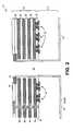
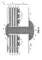
- FIG. 6illustrates a partially assembled electronic assembly 72 , including the die 10 .
- the die 10includes a plurality of bumps 66 manufactured in a similar manner.
- the die 10includes a plurality of the contact pads 16 of FIG. 5 , and a respective contact 70 is plated on each one of the contact pads 16 .
- the electronic assembly 72also includes another die 110 and a package substrate 200 .
- the die 110may be manufactured in exactly the same way as the die 10 . It may also be possible that the dies 10 and 110 are exactly the same in all respects.
- the dies 10 and 110may, for example, be identical memory dies. Alternatively, the dies 10 and 110 may differ from one another and may even be from different manufacturers.
- One diemay, for example, be a processor, and the other die a memory die.
- the die 110also includes bumps 170 and 160 at the top and the bottom, respectively. The bumps at the top may not be necessary, and merely assist in alignment during subsequent reflow.
- the die 10is stacked on the die 110 , and a respective one of the bumps 66 is positioned on a respective one of the bumps 170 .
- the package substrate 200has a plurality of contact terminals 210 on an upper surface thereof. Each one of the bumps 160 is positioned on a respective one of the contact terminals 210 .
- FIG. 7illustrates the electronic assembly 72 of FIG. 6 after being processed through a reflow furnace.
- the electronic assembly 72is heated so that the bumps 66 , 170 , and 160 melt, and are subsequently cooled.
- the bumps 66thereby attach to the bumps 170 to form interconnects 300 .
- the interconnects 300structurally attach the die 10 to the die 110 .
- the interconnects 300also electrically connect the integrated circuit of the die 10 with the integrated circuit of the die 110 .
- Other bumps 160attach the die 110 to the package substrate 200 and interconnect the integrated circuit of the die 110 with metallization layers in the package substrate 200 .
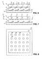
- the interconnects 300are in an array of rows and columns.
- a typical arraymay, for example, have ten rows and eight columns.
- an array of conductive memberssuch as the conductive member 60 shown in FIG. 5 are formed in an array which corresponds to the array of the interconnects 300 .
- Laser-drilling of the opening 44allows for faster throughput when compared to, for example, etching, especially if a small number of openings has to be formed.
- the opening 44is laser-drilled from an upper surface of the upper die 10 all the way through the die 10 , which allows for the use of alignment marks on an upper surface of the upper die 10 .
- the die 10provides the structural interconnection benefits of a flip-chip die, while providing the thermal benefits of a wire-bonded die. Because the integrated circuit 14 is at the top, it can be more easily cooled with a heat sink closer to the active circuitry than in a conventional flip-chip application. However, because the die 10 is structurally and electrically connected through an array of bumps 66 , the structural and electrical benefits of a flip-chip application are achieved. A further advantage of having conductive members on vias in the silicon below the integrated circuit is that they are more thermally conductive than the silicon and assist in dissipation of heat.
Landscapes
- Engineering & Computer Science (AREA)
- Microelectronics & Electronic Packaging (AREA)
- Power Engineering (AREA)
- Physics & Mathematics (AREA)
- Condensed Matter Physics & Semiconductors (AREA)
- General Physics & Mathematics (AREA)
- Computer Hardware Design (AREA)
- Manufacturing & Machinery (AREA)
- Internal Circuitry In Semiconductor Integrated Circuit Devices (AREA)
Abstract
Description
1. Field of the Invention
This invention relates to an electronic assembly of the kind having a plurality of integrated circuit dies stacked onto one another, and its manufacture.
2. Discussion of Related Art
In conventional computer assemblies, integrated circuits are “two-dimensionally” connected to one another. Two dies may, for example, be mounted to a common substrate having metal lines that interconnect the integrated circuits of the dies with one another. A “three-dimensional” interconnection scheme may in certain instances be more desirable. Handheld devices may, for example, require a more compact packaging arrangement. In other applications, the metal lines in substrates may inhibit performance. Other applications may also require a three-dimensional interconnection scheme to allow for the design of more sophisticated, three-dimensional logic.
Some techniques for forming contacts on a substrate side of a die are disclosed in U.S. Pat. No. 6,184,060. These techniques are in some respects undesirable, because they require etching of an opening in a die. Etching is relatively slow. Etching also requires many photolithographic steps. All of these factors contribute to limiting throughput.
The invention is described by way of example with reference to the accompanying drawings, wherein:
The following description relates to the construction of an electronic assembly by stacking two or more integrated circuit dies on top of one another. An opening is laser-drilled into an upper die, and subsequently filled with a conductive member. The conductive member is located on a lower die and interconnects integrated circuits of the upper and lower dies. Laser-drilling allows for faster throughput when compared to, for example, etching, especially if a smaller number of openings has to be formed. The opening is laser-drilled from an upper surface of the upper die all the way through the die, which allows for the use of alignment marks on an upper surface of the upper die.
Referring now toFIG. 1A , a portion of a fabricated wafer is shown, including adie 10 having asilicon substrate 12 and an integratedcircuit 14 formed on thesilicon substrate 12. The die10 further includes acontact pad 16 and apassivation layer 18.
Thesilicon substrate 12 has alower surface 20 and anupper surface 22.Individual transistors 24 and other electronic components are formed in and on theupper surface 22. Thesilicon substrate 12 is shown after having been thinned down in a grinding operation from between 425 and 750 microns to approximately 150 microns.
The integratedcircuit 14 has alternatingdielectric layers 32 andmetallization layers 34 that are formed on top of thesurface 22. Thecontact pad 16 and thepassivation layer 18 are formed on top of the final interlayerdielectric layer 32. Thepassivation layer 18 has a periphery that seals with thecontact pad 16 and through which an upper surface of thecontact pad 16 is exposed.
Thecontact pad 16 is connected through portions of themetallization layers 34, plugs (not shown), and vias (not shown), to thetransistors 24. Signals can thus be transmitted between thetransistors 24 and thecontact pad 16. Themetallization layers 34 are not located in acylindrical volume 38 below thecontact pad 16. There is thus no communication between thecontact pad 16 and thetransistors 24 in thecylindrical volume 38.
As illustrated inFIG. 1B , anopening 44 is subsequently laser-drilled through the die10. A triple-pumped Nd:YAG laser having a wavelength of 355 nm is preferably used to laser-drill theopening 44. A laser source of the laser is located above thepassivation layer 18, and alignment marks on an upper surface of thedie 10 is used to align the laser source with thecontact pad 16. Laser light from the laser source then strikes an upper surface of thecontact pad 16. The laser light ablates a central portion of thecontact pad 16, followed by a central portion of thecylindrical volume 38, followed by a portion in thesubstrate 12. The opening44 may be between 25 and 50 microns in diameter. In the case of a small opening such as a 25-micron opening, the opening is typically percussion-drilled. A larger opening such as a 50-micron opening may require circular movement of the laser light about a final center line of thefinal opening 44. Such circular motion is generally referred to in the art as “trapan” movement.
As shown inFIG. 2 , anoxide layer 48 is deposited on the die10. Theoxide layer 48 is blanket-deposited so that it covers thelower surface 20 and side surfaces of theopening 44.
As illustrated inFIG. 3 , atantalum nitride layer 56 is subsequently blanket-deposited on theoxide layer 48. Thetantalum nitride layer 56 forms on side surfaces of theopening 44 and on a lower surface of theoxide layer 48. Theoxide layer 48 provides a surface onto which thetantalum nitride layer 56 can easily be sputtered, and also provides electrical insulation between thetantalum nitride layer 56 and the surrounding silicon. Techniques exist in the art for sputtering tantalum nitride on oxide within openings such as theopening 44.
Thecopper conductive member 60 is plated on the remainingtantalum nitride layer 56. Thetantalum nitride layer 56 acts as a seed layer for forming theconductive member 60. Because theopening 44 extends all the way through thedie 10, a plating solution can easily be introduced into theopening 44. Thetantalum nitride layer 56 also acts as a barrier layer, preventing migration of copper from theconductive member 60 into the silicon of thesubstrate 12.
Plating is continued until theopening 44 is filled with aportion 64 of theconductive member 60 and until theconductive member 60 forms abump 66 on thecontact pad 62. Theportion 64 forms a via extending all the way through theintegrated circuit 14 and thesubstrate 12. Thebump 66 has alower surface 68 standing proud of the lower surface of theoxide layer 48. What should be noted is that theportion 64 is still electrically disconnected from thecontact pad 16 and from the metallization layers34.
As illustrated inFIG. 5 , acontact 70 is subsequently screen-printed on thedie 10. A lower surface of thecontact 70 has a central region that is in contact with an upper end of theportion 64 of theconductive member 60. An annular outer region of thecontact 70 is in contact with thecontact pad 16. Thecontact pad 16 is thereby electrically connected through thecontact 70 to theconductive member 60. A signal can now be transmitted between thebump 66 and thecontact pad 16.
Theelectronic assembly 72 also includes anotherdie 110 and apackage substrate 200. Thedie 110 may be manufactured in exactly the same way as thedie 10. It may also be possible that the dies10 and110 are exactly the same in all respects. The dies10 and110 may, for example, be identical memory dies. Alternatively, the dies10 and110 may differ from one another and may even be from different manufacturers. One die may, for example, be a processor, and the other die a memory die. What should be noted is that thedie 110 also includesbumps die 10 is stacked on thedie 110, and a respective one of thebumps 66 is positioned on a respective one of thebumps 170. Thepackage substrate 200 has a plurality ofcontact terminals 210 on an upper surface thereof. Each one of thebumps 160 is positioned on a respective one of thecontact terminals 210.
As illustrated inFIG. 8 , theinterconnects 300 are in an array of rows and columns. A typical array may, for example, have ten rows and eight columns. Although only theinterconnects 300 are shown inFIG. 8 , it will be understood that an array of conductive members such as theconductive member 60 shown inFIG. 5 are formed in an array which corresponds to the array of theinterconnects 300.
Laser-drilling of theopening 44 allows for faster throughput when compared to, for example, etching, especially if a small number of openings has to be formed. Theopening 44 is laser-drilled from an upper surface of theupper die 10 all the way through thedie 10, which allows for the use of alignment marks on an upper surface of theupper die 10.
An additional benefit of theelectronic assembly 72 is that thedie 10 provides the structural interconnection benefits of a flip-chip die, while providing the thermal benefits of a wire-bonded die. Because theintegrated circuit 14 is at the top, it can be more easily cooled with a heat sink closer to the active circuitry than in a conventional flip-chip application. However, because thedie 10 is structurally and electrically connected through an array ofbumps 66, the structural and electrical benefits of a flip-chip application are achieved. A further advantage of having conductive members on vias in the silicon below the integrated circuit is that they are more thermally conductive than the silicon and assist in dissipation of heat.
While certain exemplary embodiments have been described and shown in the accompanying drawings, it is to be understood that such embodiments are merely illustrative and not restrictive of the current invention, and that this invention is not restricted to the specific constructions and arrangements shown and described since modifications may occur to those ordinarily skilled in the art.
Claims (20)
1. A method of constructing an electronic assembly, comprising:
manufacturing a first integrated circuit on a first substrate, the first integrated circuit including a plurality of transistors formed in a semiconductor material of the first substrate and the first integrated circuit and the first substrate jointly forming a first die;
laser-drilling an opening in at least the semiconductor material of the first substrate;
forming a conductive member in the opening, the conductive member in the opening of the first substrate being electrically connected to at least one of the transistors of the first integrated circuit on the first substrate; and
stacking the first die on a second component having a circuit, the first integrated circuit being connected through the conductive member to the circuit of the second component.
2. The method ofclaim 1 , wherein the opening is laser-drilled after at least a portion of the integrated circuit is manufactured.
3. The method ofclaim 2 , wherein the transistors of the integrated circuit are formed prior to laser-drilling of the opening.
4. The method ofclaim 2 , wherein the opening is formed through a volume of the first die without transistors of the integrated circuit and extends through the entire first die.
5. The method ofclaim 4 , wherein the opening is laser-drilled through the entire first die.
6. The method ofclaim 1 , further comprising:
forming an oxide layer on surfaces of the opening.
7. The method ofclaim 6 , further comprising:
forming a metal layer on the oxide layer, the conductive member being plated on the metal layer.
8. The method ofclaim 7 , wherein the metal layer is sputtered and the conductive member is plated on the metal layer.
9. The method ofclaim 7 , wherein the metal layer and the conductive member are of different materials.
10. The method ofclaim 9 , wherein the materials include tantalum nitride and copper, respectively.
11. The method ofclaim 6 , further comprising:
forming a contact on a contact terminal on the first integrated circuit, the contact interconnecting the contact terminal with the conductive member.
12. The method ofclaim 11 , wherein the contact is screen-printed.
13. The method ofclaim 1 , wherein the conductive member is located on a terminal of the second component.
14. The method ofclaim 1 , wherein a plurality of said openings are formed, a respective conductive member is formed in each opening, and the circuits are connected through the conductive members.
15. The method ofclaim 1 , wherein the second component has a second substrate and the circuit of the second component is a second integrated circuit formed on the second substrate.
16. The method ofclaim 15 , further comprising:
laser-drilling an opening in at least the second substrate; and
forming a conductive member in the opening in the second substrate.
17. The method ofclaim 1 , wherein the opening is laser-drilled through a volume of the first substrate not designated for the first integrated circuit.
18. A method of constructing an electronic assembly, comprising:
laser-drilling an opening in at least a semiconductor material of a first substrate of a first die having a first integrated circuit formed on the first substrate, the first integrated circuit including a plurality of transistors formed in the semiconductor material of the first substrate;
forming a conductive member in the opening, the conductive member in the opening of the first substrate being electrically connected to at least one of the transistors of the first integrated circuit on the first substrate; and
stacking the first die on a second component having a circuit, at least one of the transistors of the first integrated circuit being connected through the conductive member to the circuit of the second component.
19. The method ofclaim 18 , wherein the opening extends through the entire first die.
20. The method ofclaim 18 , wherein the second component has a second substrate and the circuit of the second component is a second integrated circuit formed on the second substrate, the second circuit including a plurality of transistors.
Priority Applications (2)
| Application Number | Priority Date | Filing Date | Title |
|---|---|---|---|
| US10/112,961US6848177B2 (en) | 2002-03-28 | 2002-03-28 | Integrated circuit die and an electronic assembly having a three-dimensional interconnection scheme |
| US10/996,163US7112887B2 (en) | 2002-03-28 | 2004-11-23 | Integrated circuit die and an electronic assembly having a three-dimensional interconnection scheme |
Applications Claiming Priority (1)
| Application Number | Priority Date | Filing Date | Title |
|---|---|---|---|
| US10/112,961US6848177B2 (en) | 2002-03-28 | 2002-03-28 | Integrated circuit die and an electronic assembly having a three-dimensional interconnection scheme |
Related Child Applications (1)
| Application Number | Title | Priority Date | Filing Date |
|---|---|---|---|
| US10/996,163DivisionUS7112887B2 (en) | 2002-03-28 | 2004-11-23 | Integrated circuit die and an electronic assembly having a three-dimensional interconnection scheme |
Publications (2)
| Publication Number | Publication Date |
|---|---|
| US20030210534A1 US20030210534A1 (en) | 2003-11-13 |
| US6848177B2true US6848177B2 (en) | 2005-02-01 |
Family
ID=29399176
Family Applications (2)
| Application Number | Title | Priority Date | Filing Date |
|---|---|---|---|
| US10/112,961Expired - LifetimeUS6848177B2 (en) | 2002-03-28 | 2002-03-28 | Integrated circuit die and an electronic assembly having a three-dimensional interconnection scheme |
| US10/996,163Expired - LifetimeUS7112887B2 (en) | 2002-03-28 | 2004-11-23 | Integrated circuit die and an electronic assembly having a three-dimensional interconnection scheme |
Family Applications After (1)
| Application Number | Title | Priority Date | Filing Date |
|---|---|---|---|
| US10/996,163Expired - LifetimeUS7112887B2 (en) | 2002-03-28 | 2004-11-23 | Integrated circuit die and an electronic assembly having a three-dimensional interconnection scheme |
Country Status (1)
| Country | Link |
|---|---|
| US (2) | US6848177B2 (en) |
Cited By (26)
| Publication number | Priority date | Publication date | Assignee | Title |
|---|---|---|---|---|
| US20030230805A1 (en)* | 2002-04-23 | 2003-12-18 | Sanyo Electric Co., Ltd. | Semiconductor device and manufacturing method thereof |
| US20050154980A1 (en)* | 2004-01-14 | 2005-07-14 | Xerox Corporation | System and method for dynamic document layout |
| US20060229097A1 (en)* | 2005-04-11 | 2006-10-12 | Microsoft Corporation | Computer-readable medium, method, and device for associating information with a contact |
| US20060228825A1 (en)* | 2005-04-08 | 2006-10-12 | Micron Technology, Inc. | Method and system for fabricating semiconductor components with through wire interconnects |
| US20060261446A1 (en)* | 2005-05-19 | 2006-11-23 | Micron Technology, Inc. | Backside method and system for fabricating semiconductor components with conductive interconnects |
| US20060278979A1 (en)* | 2005-06-09 | 2006-12-14 | Intel Corporation | Die stacking recessed pad wafer design |
| US20070026639A1 (en)* | 2002-10-30 | 2007-02-01 | Sanyo Electric Co., Ltd. | Manufacturing method of semiconductor device |
| US20070126091A1 (en)* | 2005-12-07 | 2007-06-07 | Wood Alan G | Semiconductor components having through wire interconnects (TWI) |
| US20070166957A1 (en)* | 2005-12-28 | 2007-07-19 | Sanyo Electric Co., Ltd | Method of manufacturing semiconductor device |
| US20070172986A1 (en)* | 2006-01-25 | 2007-07-26 | Min-Lung Huang | Three-dimensional package and method of making the same |
| US20070172983A1 (en)* | 2006-01-25 | 2007-07-26 | Min-Lung Huang | Three-dimensional package and method of making the same |
| US20070246253A1 (en)* | 2004-07-06 | 2007-10-25 | Masami Yakabe | Through Substrate, Interposer and Manufacturing Method of Through Substrate |
| US20080157361A1 (en)* | 2006-12-28 | 2008-07-03 | Micron Technology, Inc. | Semiconductor components having through interconnects and methods of fabrication |
| US20080295329A1 (en)* | 2007-05-30 | 2008-12-04 | Sriram Muthukumar | Multi-chip packaging using an interposer such as a silicon based interposer with through-silicon-vias |
| US20080295325A1 (en)* | 2007-05-30 | 2008-12-04 | Sriram Muthukumar | Multi-chip packaging using an interposer such as a silicon based interposer with through-silicon-vias |
| US20090267194A1 (en)* | 2008-04-24 | 2009-10-29 | Powertech Technology Inc. | Semiconductor chip having tsv (through silicon via) and stacked assembly including the chips |
| US20090283872A1 (en)* | 2008-05-13 | 2009-11-19 | Lin Chun-Te | Package structure of three-dimensional stacking dice and method for manufacturing the same |
| US7659612B2 (en) | 2006-04-24 | 2010-02-09 | Micron Technology, Inc. | Semiconductor components having encapsulated through wire interconnects (TWI) |
| US20100089578A1 (en)* | 2008-10-10 | 2010-04-15 | Nguyen Philip D | Prevention of Water Intrusion Into Particulates |
| US7719102B2 (en) | 2002-06-18 | 2010-05-18 | Sanyo Electric Co., Ltd. | Semiconductor device |
| US7919875B2 (en) | 2003-08-06 | 2011-04-05 | Sanyo Electric Co., Ltd. | Semiconductor device with recess portion over pad electrode |
| US20110156233A1 (en)* | 2009-12-31 | 2011-06-30 | Hynix Semiconductor Inc. | Stack package |
| US20120007251A1 (en)* | 2010-07-08 | 2012-01-12 | National Tsing Hua University | Stacked multi-chip |
| US8298944B1 (en)* | 2011-06-01 | 2012-10-30 | Texas Instruments Incorporated | Warpage control for die with protruding TSV tips during thermo-compressive bonding |
| US9432298B1 (en) | 2011-12-09 | 2016-08-30 | P4tents1, LLC | System, method, and computer program product for improving memory systems |
| US10186480B2 (en) | 2009-06-26 | 2019-01-22 | Intel Corporation | Stacked-chip packages in package-on-package apparatus, methods of assembling same, and systems containing same |
Families Citing this family (19)
| Publication number | Priority date | Publication date | Assignee | Title |
|---|---|---|---|---|
| JP3696208B2 (en)* | 2003-01-22 | 2005-09-14 | 株式会社東芝 | Semiconductor device |
| JP2004311948A (en)* | 2003-03-27 | 2004-11-04 | Seiko Epson Corp | Semiconductor device, semiconductor device, electronic device, and method of manufacturing semiconductor device |
| US7098541B2 (en)* | 2003-05-19 | 2006-08-29 | Hewlett-Packard Development Company, L.P. | Interconnect method for directly connected stacked integrated circuits |
| US8084866B2 (en)* | 2003-12-10 | 2011-12-27 | Micron Technology, Inc. | Microelectronic devices and methods for filling vias in microelectronic devices |
| JP4966487B2 (en)* | 2004-09-29 | 2012-07-04 | オンセミコンダクター・トレーディング・リミテッド | Semiconductor device and manufacturing method thereof |
| JP4847072B2 (en)* | 2005-08-26 | 2011-12-28 | 本田技研工業株式会社 | Semiconductor integrated circuit device and manufacturing method thereof |
| US8021981B2 (en)* | 2006-08-30 | 2011-09-20 | Micron Technology, Inc. | Redistribution layers for microfeature workpieces, and associated systems and methods |
| SE530415C2 (en)* | 2006-09-04 | 2008-05-27 | Nanospace Ab | Gastrustor |
| US20080131658A1 (en)* | 2006-12-05 | 2008-06-05 | Vijay Wakharkar | Electronic packages and components thereof formed by co-deposited carbon nanotubes |
| US8110899B2 (en)* | 2006-12-20 | 2012-02-07 | Intel Corporation | Method for incorporating existing silicon die into 3D integrated stack |
| US7692946B2 (en)* | 2007-06-29 | 2010-04-06 | Intel Corporation | Memory array on more than one die |
| US8350382B2 (en)* | 2007-09-21 | 2013-01-08 | Infineon Technologies Ag | Semiconductor device including electronic component coupled to a backside of a chip |
| TW200918917A (en)* | 2007-10-16 | 2009-05-01 | Compal Electronics Inc | Testing probe and electrical connection method using the same |
| US8476769B2 (en)* | 2007-10-17 | 2013-07-02 | Taiwan Semiconductor Manufacturing Company, Ltd. | Through-silicon vias and methods for forming the same |
| US8344493B2 (en)* | 2011-01-06 | 2013-01-01 | Texas Instruments Incorporated | Warpage control features on the bottomside of TSV die lateral to protruding bottomside tips |
| US8816505B2 (en) | 2011-07-29 | 2014-08-26 | Tessera, Inc. | Low stress vias |
| US20130341794A1 (en)* | 2012-06-21 | 2013-12-26 | Applied Materials, Inc. | Ultra-thin copper seed layer for electroplating into small features |
| KR101931115B1 (en) | 2012-07-05 | 2018-12-20 | 삼성전자주식회사 | Semiconductor device and method of forming the same |
| TWI615717B (en)* | 2016-01-25 | 2018-02-21 | 凌陽科技股份有限公司 | Data transmission method between high-order integrated circuit and low-order integrated circuit and integrated circuit using the same |
Citations (99)
| Publication number | Priority date | Publication date | Assignee | Title |
|---|---|---|---|---|
| US3323198A (en) | 1965-01-27 | 1967-06-06 | Texas Instruments Inc | Electrical interconnections |
| US3484341A (en) | 1966-09-07 | 1969-12-16 | Itt | Electroplated contacts for semiconductor devices |
| US3562009A (en) | 1967-02-14 | 1971-02-09 | Western Electric Co | Method of providing electrically conductive substrate through-holes |
| US3648131A (en)* | 1969-11-07 | 1972-03-07 | Ibm | Hourglass-shaped conductive connection through semiconductor structures |
| US3810129A (en) | 1972-10-19 | 1974-05-07 | Ibm | Memory system restoration |
| US3881884A (en) | 1973-10-12 | 1975-05-06 | Ibm | Method for the formation of corrosion resistant electronic interconnections |
| US3993917A (en) | 1975-05-29 | 1976-11-23 | International Business Machines Corporation | Parameter independent FET sense amplifier |
| US4016644A (en) | 1974-03-18 | 1977-04-12 | Kulite Semiconductor Products, Inc. | Methods of fabricating low pressure silicon transducers |
| US4023562A (en) | 1975-09-02 | 1977-05-17 | Case Western Reserve University | Miniature pressure transducer for medical use and assembly method |
| US4079508A (en) | 1975-08-13 | 1978-03-21 | The Board Of Trustees Of The Leland Stanford Junior University | Miniature absolute pressure transducer assembly and method |
| US4089992A (en) | 1965-10-11 | 1978-05-16 | International Business Machines Corporation | Method for depositing continuous pinhole free silicon nitride films and products produced thereby |
| US4153998A (en) | 1972-09-21 | 1979-05-15 | Rolls-Royce (1971) Limited | Probes |
| US4188258A (en) | 1978-05-18 | 1980-02-12 | Gulton Industries, Inc. | Process for fabricating strain gage transducer |
| US4205556A (en) | 1979-02-12 | 1980-06-03 | Rockwell International Corporation | Circuitry for strain sensitive apparatus |
| US4211603A (en) | 1978-05-01 | 1980-07-08 | Tektronix, Inc. | Multilayer circuit board construction and method |
| US4276533A (en) | 1979-02-02 | 1981-06-30 | Nissan Motor Company, Limited | Pressure sensor |
| US4291293A (en) | 1978-09-27 | 1981-09-22 | Hitachi, Ltd. | Semiconductor absolute pressure transducer assembly and method |
| US4348253A (en) | 1981-11-12 | 1982-09-07 | Rca Corporation | Method for fabricating via holes in a semiconductor wafer |
| US4368106A (en) | 1980-10-27 | 1983-01-11 | General Electric Company | Implantation of electrical feed-through conductors |
| US4394712A (en) | 1981-03-18 | 1983-07-19 | General Electric Company | Alignment-enhancing feed-through conductors for stackable silicon-on-sapphire wafers |
| US4403241A (en) | 1980-08-22 | 1983-09-06 | Bell Telephone Laboratories, Incorporated | Method for etching III-V semiconductors and devices made by this method |
| US4426767A (en) | 1982-01-11 | 1984-01-24 | Sperry Cororation | Selective epitaxial etch planar processing for gallium arsenide semiconductors |
| JPS5915595A (en) | 1982-07-16 | 1984-01-26 | 王子製紙株式会社 | Mirror surface metal vapor deposition paper |
| US4463336A (en) | 1981-12-28 | 1984-07-31 | United Technologies Corporation | Ultra-thin microelectronic pressure sensors |
| US4467518A (en) | 1981-05-19 | 1984-08-28 | Ibm Corporation | Process for fabrication of stacked, complementary MOS field effect transistor circuits |
| US4467521A (en) | 1983-08-15 | 1984-08-28 | Sperry Corporation | Selective epitaxial growth of gallium arsenide with selective orientation |
| US4512829A (en) | 1983-04-07 | 1985-04-23 | Satosen Co., Ltd. | Process for producing printed circuit boards |
| US4545610A (en) | 1983-11-25 | 1985-10-08 | International Business Machines Corporation | Method for forming elongated solder connections between a semiconductor device and a supporting substrate |
| US4603341A (en) | 1983-09-08 | 1986-07-29 | International Business Machines Corporation | Stacked double dense read only memory |
| US4628174A (en) | 1984-09-17 | 1986-12-09 | General Electric Company | Forming electrical conductors in long microdiameter holes |
| US4722130A (en) | 1984-11-07 | 1988-02-02 | Kabushiki Kaisha Toshiba | Method of manufacturing a semiconductor device |
| US4769738A (en) | 1986-12-12 | 1988-09-06 | Fuji Electric Co., Ltd. | Electrostatic capacitive pressure sensor |
| US4807021A (en) | 1986-03-10 | 1989-02-21 | Kabushiki Kaisha Toshiba | Semiconductor device having stacking structure |
| US4842699A (en) | 1988-05-10 | 1989-06-27 | Avantek, Inc. | Method of selective via-hole and heat sink plating using a metal mask |
| US4897708A (en) | 1986-07-17 | 1990-01-30 | Laser Dynamics, Inc. | Semiconductor wafer array |
| US4954458A (en) | 1982-06-03 | 1990-09-04 | Texas Instruments Incorporated | Method of forming a three dimensional integrated circuit structure |
| US4978639A (en) | 1989-01-10 | 1990-12-18 | Avantek, Inc. | Method for the simultaneous formation of via-holes and wraparound plating on semiconductor chips |
| US4996587A (en) | 1989-04-10 | 1991-02-26 | International Business Machines Corporation | Integrated semiconductor chip package |
| US5071792A (en) | 1990-11-05 | 1991-12-10 | Harris Corporation | Process for forming extremely thin integrated circuit dice |
| WO1992003848A2 (en) | 1990-08-28 | 1992-03-05 | Lsi Logic Europe Plc | Stacking of integrated circuits |
| US5160987A (en) | 1989-10-26 | 1992-11-03 | International Business Machines Corporation | Three-dimensional semiconductor structures formed from planar layers |
| US5166097A (en) | 1990-11-26 | 1992-11-24 | The Boeing Company | Silicon wafers containing conductive feedthroughs |
| US5191405A (en) | 1988-12-23 | 1993-03-02 | Matsushita Electric Industrial Co., Ltd. | Three-dimensional stacked lsi |
| US5200810A (en) | 1990-04-05 | 1993-04-06 | General Electric Company | High density interconnect structure with top mounted components |
| US5225771A (en) | 1988-05-16 | 1993-07-06 | Dri Technology Corp. | Making and testing an integrated circuit using high density probe points |
| US5270261A (en) | 1991-09-13 | 1993-12-14 | International Business Machines Corporation | Three dimensional multichip package methods of fabrication |
| WO1994009513A1 (en) | 1992-10-13 | 1994-04-28 | Glenn Leedy | Interconnection structure for integrated circuits and method for making same |
| US5309318A (en) | 1992-04-21 | 1994-05-03 | International Business Machines Corporation | Thermally enhanced semiconductor chip package |
| US5307942A (en) | 1991-11-29 | 1994-05-03 | Alcatel Cit | Electronic, especially telecommunication equipment rack |
| US5313097A (en) | 1992-11-16 | 1994-05-17 | International Business Machines, Corp. | High density memory module |
| US5314844A (en) | 1991-03-04 | 1994-05-24 | Kabushiki Kaisha Toshiba | Method for dicing a semiconductor wafer |
| US5322816A (en) | 1993-01-19 | 1994-06-21 | Hughes Aircraft Company | Method for forming deep conductive feedthroughs |
| US5340771A (en) | 1993-03-18 | 1994-08-23 | Lsi Logic Corporation | Techniques for providing high I/O count connections to semiconductor dies |
| US5355283A (en) | 1993-04-14 | 1994-10-11 | Amkor Electronics, Inc. | Ball grid array with via interconnection |
| US5357672A (en) | 1993-08-13 | 1994-10-25 | Lsi Logic Corporation | Method and system for fabricating IC packages from laminated boards and heat spreader |
| JPH06302954A (en)* | 1993-04-12 | 1994-10-28 | Tokuyama Soda Co Ltd | Manufacture of circuit board |
| WO1994025981A1 (en) | 1993-05-05 | 1994-11-10 | Siemens Aktiengesellschaft | Process for producing vertically connected semiconductor components |
| US5380681A (en) | 1994-03-21 | 1995-01-10 | United Microelectronics Corporation | Three-dimensional multichip package and methods of fabricating |
| US5399898A (en) | 1992-07-17 | 1995-03-21 | Lsi Logic Corporation | Multi-chip semiconductor arrangements using flip chip dies |
| US5414637A (en) | 1992-06-24 | 1995-05-09 | International Business Machines Corporation | Intra-module spare routing for high density electronic packages |
| US5426566A (en) | 1991-09-30 | 1995-06-20 | International Business Machines Corporation | Multichip integrated circuit packages and systems |
| US5432677A (en)* | 1993-02-09 | 1995-07-11 | Texas Instruments Incorporated | Multi-chip integrated circuit module |
| US5463246A (en) | 1988-12-29 | 1995-10-31 | Sharp Kabushiki Kaisha | Large scale high density semiconductor apparatus |
| US5466634A (en) | 1994-12-20 | 1995-11-14 | International Business Machines Corporation | Electronic modules with interconnected surface metallization layers and fabrication methods therefore |
| US5467305A (en) | 1992-03-12 | 1995-11-14 | International Business Machines Corporation | Three-dimensional direct-write EEPROM arrays and fabrication methods |
| US5468999A (en) | 1994-05-26 | 1995-11-21 | Motorola, Inc. | Liquid encapsulated ball grid array semiconductor device with fine pitch wire bonding |
| US5478781A (en) | 1993-06-21 | 1995-12-26 | International Business Machines Corporation | Polyimide-insulated cube package of stacked semiconductor device chips |
| US5489554A (en) | 1992-07-21 | 1996-02-06 | Hughes Aircraft Company | Method of making a 3-dimensional circuit assembly having electrical contacts that extend through the IC layer |
| US5494832A (en) | 1993-03-29 | 1996-02-27 | Siemens Aktiengesellschaft | Method for manufacturing a solar cell from a substrate wafer |
| US5502667A (en) | 1993-09-13 | 1996-03-26 | International Business Machines Corporation | Integrated multichip memory module structure |
| US5502333A (en) | 1994-03-30 | 1996-03-26 | International Business Machines Corporation | Semiconductor stack structures and fabrication/sparing methods utilizing programmable spare circuit |
| US5502893A (en)* | 1992-10-09 | 1996-04-02 | International Business Machines Corporation | Method of making a printing wiring board |
| US5506753A (en) | 1994-09-26 | 1996-04-09 | International Business Machines Corporation | Method and apparatus for a stress relieved electronic module |
| US5517754A (en) | 1994-06-02 | 1996-05-21 | International Business Machines Corporation | Fabrication processes for monolithic electronic modules |
| US5532519A (en) | 1994-09-14 | 1996-07-02 | International Business Machines Corporation | Cube wireability enhancement with chip-to-chip alignment and thickness control |
| WO1996021943A1 (en) | 1995-01-13 | 1996-07-18 | ZAKRYTOE AKTSIONERNOE OBSCHESTVO PROIZVODSTVENNAYA FIRMA 'Az' | Device for treating planar elements with a plasma jet |
| US5550942A (en) | 1994-07-18 | 1996-08-27 | Sheem; Sang K. | Micromachined holes for optical fiber connection |
| US5557844A (en) | 1994-11-21 | 1996-09-24 | International Business Machines Corporation | Method of preparing a printed circuit board |
| US5561622A (en) | 1993-09-13 | 1996-10-01 | International Business Machines Corporation | Integrated memory cube structure |
| US5567654A (en) | 1994-09-28 | 1996-10-22 | International Business Machines Corporation | Method and workpiece for connecting a thin layer to a monolithic electronic module's surface and associated module packaging |
| US5571754A (en) | 1995-07-26 | 1996-11-05 | International Business Machines Corporation | Method of fabrication of endcap chip with conductive, monolithic L-connect for multichip stack |
| US5596226A (en) | 1994-09-06 | 1997-01-21 | International Business Machines Corporation | Semiconductor chip having a chip metal layer and a transfer metal and corresponding electronic module |
| EP0757431A2 (en) | 1995-08-03 | 1997-02-05 | International Business Machines Corporation | Machine structures fabricated of multiple microstructure layers |
| US5615477A (en) | 1994-09-06 | 1997-04-01 | Sheldahl, Inc. | Method for interconnecting a flip chip to a printed circuit substrate |
| US5646067A (en) | 1995-06-05 | 1997-07-08 | Harris Corporation | Method of bonding wafers having vias including conductive material |
| WO1997045856A1 (en) | 1996-05-31 | 1997-12-04 | Ipec Precision, Inc. | Method for treating articles with a plasma jet |
| WO1997045862A1 (en) | 1996-05-31 | 1997-12-04 | Ipec Precision, Inc. | Non-contact holder for wafer-like articles |
| US5761802A (en)* | 1996-06-10 | 1998-06-09 | Raytheon Company | Multi-layer electrical interconnection method |
| US5843844A (en) | 1995-01-25 | 1998-12-01 | Matsushita Electric Industrial Co., Ltd. | Probe sheet and method of manufacturing the same |
| US5998292A (en) | 1997-11-12 | 1999-12-07 | International Business Machines Corporation | Method for making three dimensional circuit integration |
| US6052287A (en) | 1997-12-09 | 2000-04-18 | Sandia Corporation | Silicon ball grid array chip carrier |
| US6184060B1 (en) | 1996-10-29 | 2001-02-06 | Trusi Technologies Llc | Integrated circuits and methods for their fabrication |
| US6223432B1 (en)* | 1999-03-17 | 2001-05-01 | Micron Technology, Inc. | Method of forming dual conductive plugs |
| US6260266B1 (en)* | 1995-11-10 | 2001-07-17 | Matsushita Electric Industrial Co., Ltd. | Method of forming wire interconnection wire |
| US6314641B1 (en)* | 1999-01-21 | 2001-11-13 | Micron Technology, Inc. | Interconnect for testing semiconductor components and method of fabrication |
| US6353189B1 (en)* | 1997-04-16 | 2002-03-05 | Kabushiki Kaisha Toshiba | Wiring board, wiring board fabrication method, and semiconductor package |
| US6407341B1 (en)* | 2000-04-25 | 2002-06-18 | International Business Machines Corporation | Conductive substructures of a multilayered laminate |
| US6444576B1 (en) | 2000-06-16 | 2002-09-03 | Chartered Semiconductor Manufacturing, Ltd. | Three dimensional IC package module |
| US20030155247A1 (en) | 2002-02-19 | 2003-08-21 | Shipley Company, L.L.C. | Process for electroplating silicon wafers |
Family Cites Families (4)
| Publication number | Priority date | Publication date | Assignee | Title |
|---|---|---|---|---|
| JPS5915595B2 (en) | 1979-02-20 | 1984-04-10 | 松下電器産業株式会社 | vertical synchronizer |
| CA2045788A1 (en)* | 1990-06-29 | 1991-12-30 | Kadangode K. Ramakrishnan | Cache arrangement for file system in digital data processing system |
| US6639155B1 (en)* | 1997-06-11 | 2003-10-28 | International Business Machines Corporation | High performance packaging platform and method of making same |
| JP4529262B2 (en)* | 2000-09-14 | 2010-08-25 | ソニー株式会社 | High frequency module device and manufacturing method thereof |
- 2002
- 2002-03-28USUS10/112,961patent/US6848177B2/ennot_activeExpired - Lifetime
- 2004
- 2004-11-23USUS10/996,163patent/US7112887B2/ennot_activeExpired - Lifetime
Patent Citations (108)
| Publication number | Priority date | Publication date | Assignee | Title |
|---|---|---|---|---|
| US3323198A (en) | 1965-01-27 | 1967-06-06 | Texas Instruments Inc | Electrical interconnections |
| US4089992A (en) | 1965-10-11 | 1978-05-16 | International Business Machines Corporation | Method for depositing continuous pinhole free silicon nitride films and products produced thereby |
| US3484341A (en) | 1966-09-07 | 1969-12-16 | Itt | Electroplated contacts for semiconductor devices |
| US3562009A (en) | 1967-02-14 | 1971-02-09 | Western Electric Co | Method of providing electrically conductive substrate through-holes |
| US3648131A (en)* | 1969-11-07 | 1972-03-07 | Ibm | Hourglass-shaped conductive connection through semiconductor structures |
| US4153998A (en) | 1972-09-21 | 1979-05-15 | Rolls-Royce (1971) Limited | Probes |
| US3810129A (en) | 1972-10-19 | 1974-05-07 | Ibm | Memory system restoration |
| US3811117A (en) | 1972-10-19 | 1974-05-14 | Ibm | Time ordered memory system and operation |
| US3881884A (en) | 1973-10-12 | 1975-05-06 | Ibm | Method for the formation of corrosion resistant electronic interconnections |
| US4016644A (en) | 1974-03-18 | 1977-04-12 | Kulite Semiconductor Products, Inc. | Methods of fabricating low pressure silicon transducers |
| US3993917A (en) | 1975-05-29 | 1976-11-23 | International Business Machines Corporation | Parameter independent FET sense amplifier |
| US4079508A (en) | 1975-08-13 | 1978-03-21 | The Board Of Trustees Of The Leland Stanford Junior University | Miniature absolute pressure transducer assembly and method |
| US4023562A (en) | 1975-09-02 | 1977-05-17 | Case Western Reserve University | Miniature pressure transducer for medical use and assembly method |
| US4211603A (en) | 1978-05-01 | 1980-07-08 | Tektronix, Inc. | Multilayer circuit board construction and method |
| US4188258A (en) | 1978-05-18 | 1980-02-12 | Gulton Industries, Inc. | Process for fabricating strain gage transducer |
| US4291293A (en) | 1978-09-27 | 1981-09-22 | Hitachi, Ltd. | Semiconductor absolute pressure transducer assembly and method |
| US4276533A (en) | 1979-02-02 | 1981-06-30 | Nissan Motor Company, Limited | Pressure sensor |
| US4205556A (en) | 1979-02-12 | 1980-06-03 | Rockwell International Corporation | Circuitry for strain sensitive apparatus |
| US4403241A (en) | 1980-08-22 | 1983-09-06 | Bell Telephone Laboratories, Incorporated | Method for etching III-V semiconductors and devices made by this method |
| US4368106A (en) | 1980-10-27 | 1983-01-11 | General Electric Company | Implantation of electrical feed-through conductors |
| US4394712A (en) | 1981-03-18 | 1983-07-19 | General Electric Company | Alignment-enhancing feed-through conductors for stackable silicon-on-sapphire wafers |
| US4467518A (en) | 1981-05-19 | 1984-08-28 | Ibm Corporation | Process for fabrication of stacked, complementary MOS field effect transistor circuits |
| US4348253A (en) | 1981-11-12 | 1982-09-07 | Rca Corporation | Method for fabricating via holes in a semiconductor wafer |
| US4463336A (en) | 1981-12-28 | 1984-07-31 | United Technologies Corporation | Ultra-thin microelectronic pressure sensors |
| US4426767A (en) | 1982-01-11 | 1984-01-24 | Sperry Cororation | Selective epitaxial etch planar processing for gallium arsenide semiconductors |
| US4954458A (en) | 1982-06-03 | 1990-09-04 | Texas Instruments Incorporated | Method of forming a three dimensional integrated circuit structure |
| JPS5915595A (en) | 1982-07-16 | 1984-01-26 | 王子製紙株式会社 | Mirror surface metal vapor deposition paper |
| US4512829A (en) | 1983-04-07 | 1985-04-23 | Satosen Co., Ltd. | Process for producing printed circuit boards |
| US4467521A (en) | 1983-08-15 | 1984-08-28 | Sperry Corporation | Selective epitaxial growth of gallium arsenide with selective orientation |
| US4603341A (en) | 1983-09-08 | 1986-07-29 | International Business Machines Corporation | Stacked double dense read only memory |
| US4545610A (en) | 1983-11-25 | 1985-10-08 | International Business Machines Corporation | Method for forming elongated solder connections between a semiconductor device and a supporting substrate |
| US4628174A (en) | 1984-09-17 | 1986-12-09 | General Electric Company | Forming electrical conductors in long microdiameter holes |
| US4722130A (en) | 1984-11-07 | 1988-02-02 | Kabushiki Kaisha Toshiba | Method of manufacturing a semiconductor device |
| US4807021A (en) | 1986-03-10 | 1989-02-21 | Kabushiki Kaisha Toshiba | Semiconductor device having stacking structure |
| US4897708A (en) | 1986-07-17 | 1990-01-30 | Laser Dynamics, Inc. | Semiconductor wafer array |
| US4769738A (en) | 1986-12-12 | 1988-09-06 | Fuji Electric Co., Ltd. | Electrostatic capacitive pressure sensor |
| US4842699A (en) | 1988-05-10 | 1989-06-27 | Avantek, Inc. | Method of selective via-hole and heat sink plating using a metal mask |
| US5654127A (en) | 1988-05-16 | 1997-08-05 | Elm Technology Corporation | Method of making a tester surface with high density probe points |
| US5225771A (en) | 1988-05-16 | 1993-07-06 | Dri Technology Corp. | Making and testing an integrated circuit using high density probe points |
| US5191405A (en) | 1988-12-23 | 1993-03-02 | Matsushita Electric Industrial Co., Ltd. | Three-dimensional stacked lsi |
| US5463246A (en) | 1988-12-29 | 1995-10-31 | Sharp Kabushiki Kaisha | Large scale high density semiconductor apparatus |
| US4978639A (en) | 1989-01-10 | 1990-12-18 | Avantek, Inc. | Method for the simultaneous formation of via-holes and wraparound plating on semiconductor chips |
| US4996587A (en) | 1989-04-10 | 1991-02-26 | International Business Machines Corporation | Integrated semiconductor chip package |
| US5160987A (en) | 1989-10-26 | 1992-11-03 | International Business Machines Corporation | Three-dimensional semiconductor structures formed from planar layers |
| US5200810A (en) | 1990-04-05 | 1993-04-06 | General Electric Company | High density interconnect structure with top mounted components |
| WO1992003848A2 (en) | 1990-08-28 | 1992-03-05 | Lsi Logic Europe Plc | Stacking of integrated circuits |
| US5071792A (en) | 1990-11-05 | 1991-12-10 | Harris Corporation | Process for forming extremely thin integrated circuit dice |
| US5166097A (en) | 1990-11-26 | 1992-11-24 | The Boeing Company | Silicon wafers containing conductive feedthroughs |
| US5314844A (en) | 1991-03-04 | 1994-05-24 | Kabushiki Kaisha Toshiba | Method for dicing a semiconductor wafer |
| US5270261A (en) | 1991-09-13 | 1993-12-14 | International Business Machines Corporation | Three dimensional multichip package methods of fabrication |
| US5426566A (en) | 1991-09-30 | 1995-06-20 | International Business Machines Corporation | Multichip integrated circuit packages and systems |
| US5307942A (en) | 1991-11-29 | 1994-05-03 | Alcatel Cit | Electronic, especially telecommunication equipment rack |
| US5468663A (en) | 1992-03-12 | 1995-11-21 | International Business Machines Corporation | Method of fabricating three-dimensional direct-write EEPROM arrays |
| US5467305A (en) | 1992-03-12 | 1995-11-14 | International Business Machines Corporation | Three-dimensional direct-write EEPROM arrays and fabrication methods |
| US5309318A (en) | 1992-04-21 | 1994-05-03 | International Business Machines Corporation | Thermally enhanced semiconductor chip package |
| US5414637A (en) | 1992-06-24 | 1995-05-09 | International Business Machines Corporation | Intra-module spare routing for high density electronic packages |
| US5399898A (en) | 1992-07-17 | 1995-03-21 | Lsi Logic Corporation | Multi-chip semiconductor arrangements using flip chip dies |
| US5489554A (en) | 1992-07-21 | 1996-02-06 | Hughes Aircraft Company | Method of making a 3-dimensional circuit assembly having electrical contacts that extend through the IC layer |
| US5502893A (en)* | 1992-10-09 | 1996-04-02 | International Business Machines Corporation | Method of making a printing wiring board |
| US5323035A (en) | 1992-10-13 | 1994-06-21 | Glenn Leedy | Interconnection structure for integrated circuits and method for making same |
| WO1994009513A1 (en) | 1992-10-13 | 1994-04-28 | Glenn Leedy | Interconnection structure for integrated circuits and method for making same |
| US5453404A (en) | 1992-10-13 | 1995-09-26 | Leedy; Glenn | Method for making an interconnection structure for integrated circuits |
| US5313097A (en) | 1992-11-16 | 1994-05-17 | International Business Machines, Corp. | High density memory module |
| US5322816A (en) | 1993-01-19 | 1994-06-21 | Hughes Aircraft Company | Method for forming deep conductive feedthroughs |
| US5432677A (en)* | 1993-02-09 | 1995-07-11 | Texas Instruments Incorporated | Multi-chip integrated circuit module |
| US5340771A (en) | 1993-03-18 | 1994-08-23 | Lsi Logic Corporation | Techniques for providing high I/O count connections to semiconductor dies |
| US5494832A (en) | 1993-03-29 | 1996-02-27 | Siemens Aktiengesellschaft | Method for manufacturing a solar cell from a substrate wafer |
| JPH06302954A (en)* | 1993-04-12 | 1994-10-28 | Tokuyama Soda Co Ltd | Manufacture of circuit board |
| US5355283A (en) | 1993-04-14 | 1994-10-11 | Amkor Electronics, Inc. | Ball grid array with via interconnection |
| WO1994025981A1 (en) | 1993-05-05 | 1994-11-10 | Siemens Aktiengesellschaft | Process for producing vertically connected semiconductor components |
| EP0698288B1 (en) | 1993-05-05 | 1998-08-05 | Siemens Aktiengesellschaft | Process for producing vertically connected semiconductor components |
| US5478781A (en) | 1993-06-21 | 1995-12-26 | International Business Machines Corporation | Polyimide-insulated cube package of stacked semiconductor device chips |
| US5357672A (en) | 1993-08-13 | 1994-10-25 | Lsi Logic Corporation | Method and system for fabricating IC packages from laminated boards and heat spreader |
| US5563086A (en) | 1993-09-13 | 1996-10-08 | International Business Machines Corporation | Integrated memory cube, structure and fabrication |
| US5502667A (en) | 1993-09-13 | 1996-03-26 | International Business Machines Corporation | Integrated multichip memory module structure |
| US5561622A (en) | 1993-09-13 | 1996-10-01 | International Business Machines Corporation | Integrated memory cube structure |
| US5380681A (en) | 1994-03-21 | 1995-01-10 | United Microelectronics Corporation | Three-dimensional multichip package and methods of fabricating |
| US5502333A (en) | 1994-03-30 | 1996-03-26 | International Business Machines Corporation | Semiconductor stack structures and fabrication/sparing methods utilizing programmable spare circuit |
| US5468999A (en) | 1994-05-26 | 1995-11-21 | Motorola, Inc. | Liquid encapsulated ball grid array semiconductor device with fine pitch wire bonding |
| US5517754A (en) | 1994-06-02 | 1996-05-21 | International Business Machines Corporation | Fabrication processes for monolithic electronic modules |
| US5550942A (en) | 1994-07-18 | 1996-08-27 | Sheem; Sang K. | Micromachined holes for optical fiber connection |
| US5615477A (en) | 1994-09-06 | 1997-04-01 | Sheldahl, Inc. | Method for interconnecting a flip chip to a printed circuit substrate |
| US5596226A (en) | 1994-09-06 | 1997-01-21 | International Business Machines Corporation | Semiconductor chip having a chip metal layer and a transfer metal and corresponding electronic module |
| US5567653A (en) | 1994-09-14 | 1996-10-22 | International Business Machines Corporation | Process for aligning etch masks on an integrated circuit surface using electromagnetic energy |
| US5532519A (en) | 1994-09-14 | 1996-07-02 | International Business Machines Corporation | Cube wireability enhancement with chip-to-chip alignment and thickness control |
| US5506753A (en) | 1994-09-26 | 1996-04-09 | International Business Machines Corporation | Method and apparatus for a stress relieved electronic module |
| US5567654A (en) | 1994-09-28 | 1996-10-22 | International Business Machines Corporation | Method and workpiece for connecting a thin layer to a monolithic electronic module's surface and associated module packaging |
| US5557844A (en) | 1994-11-21 | 1996-09-24 | International Business Machines Corporation | Method of preparing a printed circuit board |
| US5517057A (en) | 1994-12-20 | 1996-05-14 | International Business Machines Corporation | Electronic modules with interconnected surface metallization layers |
| US5466634A (en) | 1994-12-20 | 1995-11-14 | International Business Machines Corporation | Electronic modules with interconnected surface metallization layers and fabrication methods therefore |
| WO1996021943A1 (en) | 1995-01-13 | 1996-07-18 | ZAKRYTOE AKTSIONERNOE OBSCHESTVO PROIZVODSTVENNAYA FIRMA 'Az' | Device for treating planar elements with a plasma jet |
| US5843844A (en) | 1995-01-25 | 1998-12-01 | Matsushita Electric Industrial Co., Ltd. | Probe sheet and method of manufacturing the same |
| US5646067A (en) | 1995-06-05 | 1997-07-08 | Harris Corporation | Method of bonding wafers having vias including conductive material |
| US5571754A (en) | 1995-07-26 | 1996-11-05 | International Business Machines Corporation | Method of fabrication of endcap chip with conductive, monolithic L-connect for multichip stack |
| EP0757431A2 (en) | 1995-08-03 | 1997-02-05 | International Business Machines Corporation | Machine structures fabricated of multiple microstructure layers |
| US6260266B1 (en)* | 1995-11-10 | 2001-07-17 | Matsushita Electric Industrial Co., Ltd. | Method of forming wire interconnection wire |
| WO1997045856A1 (en) | 1996-05-31 | 1997-12-04 | Ipec Precision, Inc. | Method for treating articles with a plasma jet |
| WO1997045862A1 (en) | 1996-05-31 | 1997-12-04 | Ipec Precision, Inc. | Non-contact holder for wafer-like articles |
| US5761802A (en)* | 1996-06-10 | 1998-06-09 | Raytheon Company | Multi-layer electrical interconnection method |
| US6184060B1 (en) | 1996-10-29 | 2001-02-06 | Trusi Technologies Llc | Integrated circuits and methods for their fabrication |
| US6353189B1 (en)* | 1997-04-16 | 2002-03-05 | Kabushiki Kaisha Toshiba | Wiring board, wiring board fabrication method, and semiconductor package |
| US5998292A (en) | 1997-11-12 | 1999-12-07 | International Business Machines Corporation | Method for making three dimensional circuit integration |
| US6052287A (en) | 1997-12-09 | 2000-04-18 | Sandia Corporation | Silicon ball grid array chip carrier |
| US6314641B1 (en)* | 1999-01-21 | 2001-11-13 | Micron Technology, Inc. | Interconnect for testing semiconductor components and method of fabrication |
| US6223432B1 (en)* | 1999-03-17 | 2001-05-01 | Micron Technology, Inc. | Method of forming dual conductive plugs |
| US6407341B1 (en)* | 2000-04-25 | 2002-06-18 | International Business Machines Corporation | Conductive substructures of a multilayered laminate |
| US6444576B1 (en) | 2000-06-16 | 2002-09-03 | Chartered Semiconductor Manufacturing, Ltd. | Three dimensional IC package module |
| US20030155247A1 (en) | 2002-02-19 | 2003-08-21 | Shipley Company, L.L.C. | Process for electroplating silicon wafers |
Non-Patent Citations (6)
| Title |
|---|
| Anthony, Thomas R., "Forming Feedthroughs in Laser-Drilled Holes in Semiconductor Wafers by Double-Sided Sputtering," IEEE Trans. On Comp., Hybrids, & Mfg. Tech., Mar. 1982, pp. 171-180, vol. CHMT-5, No. 1. |
| AZ Corporation, "Plasma Jet Etching Technology and Equipment; Silicon Wafer Thinning and Isotropical Etching at Atmospheric Pressure," Semicon/Europe, Apr. 1995, 4 pages, Geneva, Switzerland. |
| Christenson, C., et al., "Wafer Through-Hole Interconnections with High Vertical Wiring Densities," IEEE Trans. On Comp., Pkg. & Mfg. Tech., Dec. 1996, pp. 516-521, vol. 19, No. 4, Part A. |
| IPEC Precision brochure for PACEJET II ((C) 1996), 2 pages. |
| Siniaguine, O., et al., "Plasma Processing of Silicon Wafers at Atmospheric Pressure," Electronic Industry, Jun. 1994, pp. 27-30 (not translated). |
| Siniaguine, Oleg, "Plasma Jet Etching at Atmospheric Pressure for Semiconductor Production," First International Symposium on Plasma Process-Induced Damage, May 13-14, 1996, Santa Clara, California, pp. 151-153. |
Cited By (86)
| Publication number | Priority date | Publication date | Assignee | Title |
|---|---|---|---|---|
| US20030230805A1 (en)* | 2002-04-23 | 2003-12-18 | Sanyo Electric Co., Ltd. | Semiconductor device and manufacturing method thereof |
| US20040235270A1 (en)* | 2002-04-23 | 2004-11-25 | Sanyo Electric Co., Ltd. | Method of manufacturing semiconductor device |
| US7312521B2 (en) | 2002-04-23 | 2007-12-25 | Sanyo Electric Co., Ltd. | Semiconductor device with holding member |
| US20060033198A1 (en)* | 2002-04-23 | 2006-02-16 | Sanyo Electric Co., Ltd. | Semiconductor device with sidewall wiring |
| US8105856B2 (en)* | 2002-04-23 | 2012-01-31 | Semiconductor Components Industries, Llc | Method of manufacturing semiconductor device with wiring on side surface thereof |
| US7271466B2 (en) | 2002-04-23 | 2007-09-18 | Sanyo Electric Co., Ltd. | Semiconductor device with sidewall wiring |
| US7719102B2 (en) | 2002-06-18 | 2010-05-18 | Sanyo Electric Co., Ltd. | Semiconductor device |
| US20070026639A1 (en)* | 2002-10-30 | 2007-02-01 | Sanyo Electric Co., Ltd. | Manufacturing method of semiconductor device |
| US7662670B2 (en) | 2002-10-30 | 2010-02-16 | Sanyo Electric Co., Ltd. | Manufacturing method of semiconductor device |
| US7919875B2 (en) | 2003-08-06 | 2011-04-05 | Sanyo Electric Co., Ltd. | Semiconductor device with recess portion over pad electrode |
| US20050154980A1 (en)* | 2004-01-14 | 2005-07-14 | Xerox Corporation | System and method for dynamic document layout |
| US7866038B2 (en)* | 2004-07-06 | 2011-01-11 | Tokyo Electron Limited | Through substrate, interposer and manufacturing method of through substrate |
| US20070246253A1 (en)* | 2004-07-06 | 2007-10-25 | Masami Yakabe | Through Substrate, Interposer and Manufacturing Method of Through Substrate |
| US7728443B2 (en) | 2005-04-08 | 2010-06-01 | Micron Technology, Inc. | Semiconductor components with through wire interconnects |
| US20060228825A1 (en)* | 2005-04-08 | 2006-10-12 | Micron Technology, Inc. | Method and system for fabricating semiconductor components with through wire interconnects |
| US7757385B2 (en) | 2005-04-08 | 2010-07-20 | Micron Technology, Inc. | System for fabricating semiconductor components with through wire interconnects |
| US20070200255A1 (en)* | 2005-04-08 | 2007-08-30 | Hembree David R | System for fabricating semiconductor components with through wire interconnects |
| US20070202617A1 (en)* | 2005-04-08 | 2007-08-30 | Hembree David R | Method for fabricating stacked semiconductor components with through wire interconnects |
| US20100140753A1 (en)* | 2005-04-08 | 2010-06-10 | Hembree David R | Stacked Semiconductor Component Having Through Wire Interconnect And Method Of Fabrication |
| US20070222054A1 (en)* | 2005-04-08 | 2007-09-27 | Hembree David R | Semiconductor components with through wire interconnects |
| US7682962B2 (en) | 2005-04-08 | 2010-03-23 | Micron Technology, Inc. | Method for fabricating stacked semiconductor components with through wire interconnects |
| US7919846B2 (en) | 2005-04-08 | 2011-04-05 | Micron Technology, Inc. | Stacked semiconductor component having through wire interconnect |
| US20110108959A1 (en)* | 2005-04-08 | 2011-05-12 | Hembree David R | Semiconductor Component Having Through Wire Interconnect With Compressed Bump |
| US8053909B2 (en) | 2005-04-08 | 2011-11-08 | Micron Technology, Inc. | Semiconductor component having through wire interconnect with compressed bump |
| US7371676B2 (en) | 2005-04-08 | 2008-05-13 | Micron Technology, Inc. | Method for fabricating semiconductor components with through wire interconnects |
| US20060229097A1 (en)* | 2005-04-11 | 2006-10-12 | Microsoft Corporation | Computer-readable medium, method, and device for associating information with a contact |
| WO2006124295A3 (en)* | 2005-05-19 | 2007-06-28 | Micron Technology Inc | Backside method and system for fabricating semiconductor components with conductive interconnects |
| US7727872B2 (en) | 2005-05-19 | 2010-06-01 | Micron Technology, Inc. | Methods for fabricating semiconductor components with conductive interconnects |
| US7768096B2 (en) | 2005-05-19 | 2010-08-03 | Micron Technology, Inc. | System for fabricating semiconductor components with conductive interconnects |
| US8546931B2 (en) | 2005-05-19 | 2013-10-01 | Micron Technology, Inc. | Stacked semiconductor components having conductive interconnects |
| US20060261446A1 (en)* | 2005-05-19 | 2006-11-23 | Micron Technology, Inc. | Backside method and system for fabricating semiconductor components with conductive interconnects |
| US20110175223A1 (en)* | 2005-05-19 | 2011-07-21 | Wood Alan G | Stacked Semiconductor Components Having Conductive Interconnects |
| US7951702B2 (en) | 2005-05-19 | 2011-05-31 | Micron Technology, Inc. | Methods for fabricating semiconductor components with conductive interconnects having planar surfaces |
| US20080206990A1 (en)* | 2005-05-19 | 2008-08-28 | Wood Alan G | Methods For Fabricating Semiconductor Components With Conductive Interconnects |
| US7393770B2 (en) | 2005-05-19 | 2008-07-01 | Micron Technology, Inc. | Backside method for fabricating semiconductor components with conductive interconnects |
| US7935991B2 (en) | 2005-05-19 | 2011-05-03 | Micron Technology, Inc. | Semiconductor components with conductive interconnects |
| US20060278979A1 (en)* | 2005-06-09 | 2006-12-14 | Intel Corporation | Die stacking recessed pad wafer design |
| US8193646B2 (en) | 2005-12-07 | 2012-06-05 | Micron Technology, Inc. | Semiconductor component having through wire interconnect (TWI) with compressed wire |
| US7579267B2 (en) | 2005-12-07 | 2009-08-25 | Micron Technology, Inc. | Methods and systems for fabricating semiconductor components with through wire interconnects (TWI) |
| US20070167000A1 (en)* | 2005-12-07 | 2007-07-19 | Wood Alan G | Methods and systems for fabricating semiconductor components with through wire interconnects (TWI) |
| US20080042247A1 (en)* | 2005-12-07 | 2008-02-21 | Wood Alan G | Stacked Semiconductor Components With Through Wire Interconnects (TWI) |
| US20070126091A1 (en)* | 2005-12-07 | 2007-06-07 | Wood Alan G | Semiconductor components having through wire interconnects (TWI) |
| US8513797B2 (en) | 2005-12-07 | 2013-08-20 | Micron Technology, Inc. | Stacked semiconductor component having through wire interconnect (TWI) with compressed wire |
| US20100264521A1 (en)* | 2005-12-07 | 2010-10-21 | Wood Alan G | Semiconductor Component Having Through Wire Interconnect (TWI) With Compressed Wire |
| US9013044B2 (en) | 2005-12-07 | 2015-04-21 | Micron Technology, Inc. | Through wire interconnect (TWI) for semiconductor components having wire in via and bonded connection with substrate contact |
| US7307348B2 (en) | 2005-12-07 | 2007-12-11 | Micron Technology, Inc. | Semiconductor components having through wire interconnects (TWI) |
| US7786605B2 (en) | 2005-12-07 | 2010-08-31 | Micron Technology, Inc. | Stacked semiconductor components with through wire interconnects (TWI) |
| US20070166957A1 (en)* | 2005-12-28 | 2007-07-19 | Sanyo Electric Co., Ltd | Method of manufacturing semiconductor device |
| US7795115B2 (en) | 2005-12-28 | 2010-09-14 | Sanyo Electric Co., Ltd. | Method of manufacturing semiconductor device |
| US7528053B2 (en) | 2006-01-25 | 2009-05-05 | Advanced Semiconductor Engineering, Inc. | Three-dimensional package and method of making the same |
| US20070172983A1 (en)* | 2006-01-25 | 2007-07-26 | Min-Lung Huang | Three-dimensional package and method of making the same |
| US20070172985A1 (en)* | 2006-01-25 | 2007-07-26 | Min-Lung Huang | Three-dimensional package and method of making the same |
| US7446404B2 (en) | 2006-01-25 | 2008-11-04 | Advanced Semiconductor Engineering, Inc. | Three-dimensional package and method of making the same |
| US7741152B2 (en) | 2006-01-25 | 2010-06-22 | Advanced Semiconductor Engineering, Inc. | Three-dimensional package and method of making the same |
| US20070172986A1 (en)* | 2006-01-25 | 2007-07-26 | Min-Lung Huang | Three-dimensional package and method of making the same |
| US8120167B2 (en) | 2006-04-24 | 2012-02-21 | Micron Technology, Inc. | System with semiconductor components having encapsulated through wire interconnects (TWI) |
| US7883908B2 (en) | 2006-04-24 | 2011-02-08 | Micron Technology, Inc. | Method for fabricating semiconductor component having encapsulated through wire interconnect (TWI) |
| US9018751B2 (en) | 2006-04-24 | 2015-04-28 | Micron Technology, Inc. | Semiconductor module system having encapsulated through wire interconnect (TWI) |
| US20100047934A1 (en)* | 2006-04-24 | 2010-02-25 | Hembree David R | Method For Fabricating Semiconductor Component Having Encapsulated Through Wire Interconnect (TWI) |
| US7659612B2 (en) | 2006-04-24 | 2010-02-09 | Micron Technology, Inc. | Semiconductor components having encapsulated through wire interconnects (TWI) |
| US8217510B2 (en) | 2006-04-24 | 2012-07-10 | Micron Technology, Inc. | Semiconductor module system having stacked components with encapsulated through wire interconnects (TWI) |
| US8581387B1 (en) | 2006-04-24 | 2013-11-12 | Micron Technology, Inc. | Through wire interconnect (TWI) having bonded connection and encapsulating polymer layer |
| US8404523B2 (en) | 2006-04-24 | 2013-03-26 | Micron Technoloy, Inc. | Method for fabricating stacked semiconductor system with encapsulated through wire interconnects (TWI) |
| US8741667B2 (en) | 2006-04-24 | 2014-06-03 | Micron Technology, Inc. | Method for fabricating a through wire interconnect (TWI) on a semiconductor substrate having a bonded connection and an encapsulating polymer layer |
| US7538413B2 (en) | 2006-12-28 | 2009-05-26 | Micron Technology, Inc. | Semiconductor components having through interconnects |
| US7833832B2 (en) | 2006-12-28 | 2010-11-16 | Micron Technology, Inc. | Method of fabricating semiconductor components with through interconnects |
| US20080157361A1 (en)* | 2006-12-28 | 2008-07-03 | Micron Technology, Inc. | Semiconductor components having through interconnects and methods of fabrication |
| US20080295325A1 (en)* | 2007-05-30 | 2008-12-04 | Sriram Muthukumar | Multi-chip packaging using an interposer such as a silicon based interposer with through-silicon-vias |
| US20080295329A1 (en)* | 2007-05-30 | 2008-12-04 | Sriram Muthukumar | Multi-chip packaging using an interposer such as a silicon based interposer with through-silicon-vias |
| US20110067236A1 (en)* | 2007-05-30 | 2011-03-24 | Sriram Muthukumar | Multi-chip packaging using an interposer such as a silicon based interposer with through-silicon-vias |
| US7882628B2 (en) | 2007-05-30 | 2011-02-08 | Intel Corporation | Multi-chip packaging using an interposer such as a silicon based interposer with through-silicon-vias |
| US7841080B2 (en) | 2007-05-30 | 2010-11-30 | Intel Corporation | Multi-chip packaging using an interposer with through-vias |
| US8387240B2 (en) | 2007-05-30 | 2013-03-05 | Intel Corporation | Methods for making multi-chip packaging using an interposer |
| US20090267194A1 (en)* | 2008-04-24 | 2009-10-29 | Powertech Technology Inc. | Semiconductor chip having tsv (through silicon via) and stacked assembly including the chips |
| US7838967B2 (en)* | 2008-04-24 | 2010-11-23 | Powertech Technology Inc. | Semiconductor chip having TSV (through silicon via) and stacked assembly including the chips |
| US8531009B2 (en) | 2008-05-13 | 2013-09-10 | Industrial Technology Research Institute | Package structure of three-dimensional stacking dice and method for manufacturing the same |
| US20090283872A1 (en)* | 2008-05-13 | 2009-11-19 | Lin Chun-Te | Package structure of three-dimensional stacking dice and method for manufacturing the same |
| US20100089578A1 (en)* | 2008-10-10 | 2010-04-15 | Nguyen Philip D | Prevention of Water Intrusion Into Particulates |
| US10186480B2 (en) | 2009-06-26 | 2019-01-22 | Intel Corporation | Stacked-chip packages in package-on-package apparatus, methods of assembling same, and systems containing same |
| US11217516B2 (en) | 2009-06-26 | 2022-01-04 | Intel Corporation | Stacked-chip packages in package-on-package apparatus, methods of assembling same, and systems containing same |
| US8110910B2 (en)* | 2009-12-31 | 2012-02-07 | Hynix Semiconductor Inc. | Stack package |
| US20110156233A1 (en)* | 2009-12-31 | 2011-06-30 | Hynix Semiconductor Inc. | Stack package |
| US8174126B2 (en)* | 2010-07-08 | 2012-05-08 | National Tsing Hua University | Stacked multi-chip |
| US20120007251A1 (en)* | 2010-07-08 | 2012-01-12 | National Tsing Hua University | Stacked multi-chip |
| US8298944B1 (en)* | 2011-06-01 | 2012-10-30 | Texas Instruments Incorporated | Warpage control for die with protruding TSV tips during thermo-compressive bonding |
| US9432298B1 (en) | 2011-12-09 | 2016-08-30 | P4tents1, LLC | System, method, and computer program product for improving memory systems |
Also Published As
| Publication number | Publication date |
|---|---|
| US7112887B2 (en) | 2006-09-26 |
| US20050090042A1 (en) | 2005-04-28 |
| US20030210534A1 (en) | 2003-11-13 |
Similar Documents
| Publication | Publication Date | Title |
|---|---|---|
| US6848177B2 (en) | Integrated circuit die and an electronic assembly having a three-dimensional interconnection scheme | |
| TWI714913B (en) | Package structure and manufacturing method thereof | |
| US7537954B2 (en) | Microelectronic assembly having thermoelectric elements to cool a die and a method of making the same | |
| US9391043B2 (en) | Semiconductor device and manufacturing method thereof | |
| US8609506B2 (en) | On-chip heat spreader | |
| US7847416B2 (en) | Wafer level package and method of fabricating the same | |
| US6352923B1 (en) | Method of fabricating direct contact through hole type | |
| US11088100B2 (en) | Semiconductor package and manufacturing method thereof | |
| US10431549B2 (en) | Semiconductor package and manufacturing method thereof | |
| CN105655312A (en) | Semiconductor including stress buffer material formed on low-K metalized system | |
| CN102820259A (en) | Semiconductor device and method of forming a power MOSFET | |
| US11935824B2 (en) | Integrated circuit package module including a bonding system | |
| US20230133322A1 (en) | Semiconductor package and method of manufacturing the same | |
| US6908845B2 (en) | Integrated circuit die and an electronic assembly having a three-dimensional interconnection scheme | |
| US20030183943A1 (en) | Integrated circuit die and an electronic assembly having a three-dimensional interconnection scheme | |
| US20240321794A1 (en) | Semiconductor chip having a through electrode and semiconductor package including the semiconductor chip | |
| US20230420415A1 (en) | Semiconductor package | |
| CN115497910B (en) | Wafer stacking structure and manufacturing method thereof | |
| US20240178112A1 (en) | Semiconductor package structure and method of forming the same | |
| US20240153919A1 (en) | Semiconductor package | |
| US20240055378A1 (en) | Semiconductor chip and semiconductor package including the same | |
| CN223108878U (en) | Semiconductor Package | |
| US20240413068A1 (en) | Semiconductor substrate and method of manufacturing the semiconductor substrate | |
| EP4535423A2 (en) | Semiconductor package structure | |
| US20250192083A1 (en) | Semiconductor package |
Legal Events
| Date | Code | Title | Description |
|---|---|---|---|
| AS | Assignment | Owner name:INTEL CORPORATION, CALIFORNIA Free format text:ASSIGNMENT OF ASSIGNORS INTEREST;ASSIGNORS:SWAN, JOHANNA M.;NATARAJAN, BALA;CHIANG, CHIEN;AND OTHERS;REEL/FRAME:013054/0215;SIGNING DATES FROM 20020605 TO 20020619 | |
| FEPP | Fee payment procedure | Free format text:PAYOR NUMBER ASSIGNED (ORIGINAL EVENT CODE: ASPN); ENTITY STATUS OF PATENT OWNER: LARGE ENTITY | |
| STCF | Information on status: patent grant | Free format text:PATENTED CASE | |
| FPAY | Fee payment | Year of fee payment:4 | |
| REMI | Maintenance fee reminder mailed | ||
| FPAY | Fee payment | Year of fee payment:8 | |
| SULP | Surcharge for late payment | Year of fee payment:7 | |
| FPAY | Fee payment | Year of fee payment:12 |