US6848173B2 - Microelectric packages having deformed bonded leads and methods therefor - Google Patents
Microelectric packages having deformed bonded leads and methods thereforDownload PDFInfo
- Publication number
- US6848173B2 US6848173B2US09/766,814US76681401AUS6848173B2US 6848173 B2US6848173 B2US 6848173B2US 76681401 AUS76681401 AUS 76681401AUS 6848173 B2US6848173 B2US 6848173B2
- Authority
- US
- United States
- Prior art keywords
- contacts
- connection component
- microelectronic element
- microelectronic
- leads
- Prior art date
- Legal status (The legal status is an assumption and is not a legal conclusion. Google has not performed a legal analysis and makes no representation as to the accuracy of the status listed.)
- Expired - Fee Related, expires
Links
Images


Classifications
- H—ELECTRICITY
- H01—ELECTRIC ELEMENTS
- H01L—SEMICONDUCTOR DEVICES NOT COVERED BY CLASS H10
- H01L24/00—Arrangements for connecting or disconnecting semiconductor or solid-state bodies; Methods or apparatus related thereto
- H01L24/01—Means for bonding being attached to, or being formed on, the surface to be connected, e.g. chip-to-package, die-attach, "first-level" interconnects; Manufacturing methods related thereto
- H01L24/26—Layer connectors, e.g. plate connectors, solder or adhesive layers; Manufacturing methods related thereto
- H01L24/28—Structure, shape, material or disposition of the layer connectors prior to the connecting process
- H01L24/29—Structure, shape, material or disposition of the layer connectors prior to the connecting process of an individual layer connector
- H—ELECTRICITY
- H01—ELECTRIC ELEMENTS
- H01L—SEMICONDUCTOR DEVICES NOT COVERED BY CLASS H10
- H01L23/00—Details of semiconductor or other solid state devices
- H01L23/48—Arrangements for conducting electric current to or from the solid state body in operation, e.g. leads, terminal arrangements ; Selection of materials therefor
- H01L23/488—Arrangements for conducting electric current to or from the solid state body in operation, e.g. leads, terminal arrangements ; Selection of materials therefor consisting of soldered or bonded constructions
- H01L23/498—Leads, i.e. metallisations or lead-frames on insulating substrates, e.g. chip carriers
- H01L23/49811—Additional leads joined to the metallisation on the insulating substrate, e.g. pins, bumps, wires, flat leads
- H—ELECTRICITY
- H01—ELECTRIC ELEMENTS
- H01L—SEMICONDUCTOR DEVICES NOT COVERED BY CLASS H10
- H01L24/00—Arrangements for connecting or disconnecting semiconductor or solid-state bodies; Methods or apparatus related thereto
- H01L24/01—Means for bonding being attached to, or being formed on, the surface to be connected, e.g. chip-to-package, die-attach, "first-level" interconnects; Manufacturing methods related thereto
- H01L24/10—Bump connectors ; Manufacturing methods related thereto
- H01L24/15—Structure, shape, material or disposition of the bump connectors after the connecting process
- H01L24/16—Structure, shape, material or disposition of the bump connectors after the connecting process of an individual bump connector
- H—ELECTRICITY
- H01—ELECTRIC ELEMENTS
- H01L—SEMICONDUCTOR DEVICES NOT COVERED BY CLASS H10
- H01L24/00—Arrangements for connecting or disconnecting semiconductor or solid-state bodies; Methods or apparatus related thereto
- H01L24/01—Means for bonding being attached to, or being formed on, the surface to be connected, e.g. chip-to-package, die-attach, "first-level" interconnects; Manufacturing methods related thereto
- H01L24/26—Layer connectors, e.g. plate connectors, solder or adhesive layers; Manufacturing methods related thereto
- H01L24/31—Structure, shape, material or disposition of the layer connectors after the connecting process
- H01L24/32—Structure, shape, material or disposition of the layer connectors after the connecting process of an individual layer connector
- H—ELECTRICITY
- H01—ELECTRIC ELEMENTS
- H01L—SEMICONDUCTOR DEVICES NOT COVERED BY CLASS H10
- H01L24/00—Arrangements for connecting or disconnecting semiconductor or solid-state bodies; Methods or apparatus related thereto
- H01L24/01—Means for bonding being attached to, or being formed on, the surface to be connected, e.g. chip-to-package, die-attach, "first-level" interconnects; Manufacturing methods related thereto
- H01L24/42—Wire connectors; Manufacturing methods related thereto
- H01L24/47—Structure, shape, material or disposition of the wire connectors after the connecting process
- H01L24/48—Structure, shape, material or disposition of the wire connectors after the connecting process of an individual wire connector
- H—ELECTRICITY
- H01—ELECTRIC ELEMENTS
- H01L—SEMICONDUCTOR DEVICES NOT COVERED BY CLASS H10
- H01L24/00—Arrangements for connecting or disconnecting semiconductor or solid-state bodies; Methods or apparatus related thereto
- H01L24/01—Means for bonding being attached to, or being formed on, the surface to be connected, e.g. chip-to-package, die-attach, "first-level" interconnects; Manufacturing methods related thereto
- H01L24/50—Tape automated bonding [TAB] connectors, i.e. film carriers; Manufacturing methods related thereto
- H—ELECTRICITY
- H01—ELECTRIC ELEMENTS
- H01L—SEMICONDUCTOR DEVICES NOT COVERED BY CLASS H10
- H01L24/00—Arrangements for connecting or disconnecting semiconductor or solid-state bodies; Methods or apparatus related thereto
- H01L24/74—Apparatus for manufacturing arrangements for connecting or disconnecting semiconductor or solid-state bodies
- H01L24/78—Apparatus for connecting with wire connectors
- H—ELECTRICITY
- H01—ELECTRIC ELEMENTS
- H01L—SEMICONDUCTOR DEVICES NOT COVERED BY CLASS H10
- H01L24/00—Arrangements for connecting or disconnecting semiconductor or solid-state bodies; Methods or apparatus related thereto
- H01L24/80—Methods for connecting semiconductor or other solid state bodies using means for bonding being attached to, or being formed on, the surface to be connected
- H01L24/83—Methods for connecting semiconductor or other solid state bodies using means for bonding being attached to, or being formed on, the surface to be connected using a layer connector
- H—ELECTRICITY
- H01—ELECTRIC ELEMENTS
- H01L—SEMICONDUCTOR DEVICES NOT COVERED BY CLASS H10
- H01L24/00—Arrangements for connecting or disconnecting semiconductor or solid-state bodies; Methods or apparatus related thereto
- H01L24/80—Methods for connecting semiconductor or other solid state bodies using means for bonding being attached to, or being formed on, the surface to be connected
- H01L24/85—Methods for connecting semiconductor or other solid state bodies using means for bonding being attached to, or being formed on, the surface to be connected using a wire connector
- H—ELECTRICITY
- H01—ELECTRIC ELEMENTS
- H01L—SEMICONDUCTOR DEVICES NOT COVERED BY CLASS H10
- H01L24/00—Arrangements for connecting or disconnecting semiconductor or solid-state bodies; Methods or apparatus related thereto
- H01L24/80—Methods for connecting semiconductor or other solid state bodies using means for bonding being attached to, or being formed on, the surface to be connected
- H01L24/86—Methods for connecting semiconductor or other solid state bodies using means for bonding being attached to, or being formed on, the surface to be connected using tape automated bonding [TAB]
- H—ELECTRICITY
- H01—ELECTRIC ELEMENTS
- H01L—SEMICONDUCTOR DEVICES NOT COVERED BY CLASS H10
- H01L25/00—Assemblies consisting of a plurality of semiconductor or other solid state devices
- H01L25/03—Assemblies consisting of a plurality of semiconductor or other solid state devices all the devices being of a type provided for in a single subclass of subclasses H10B, H10D, H10F, H10H, H10K or H10N, e.g. assemblies of rectifier diodes
- H01L25/04—Assemblies consisting of a plurality of semiconductor or other solid state devices all the devices being of a type provided for in a single subclass of subclasses H10B, H10D, H10F, H10H, H10K or H10N, e.g. assemblies of rectifier diodes the devices not having separate containers
- H01L25/065—Assemblies consisting of a plurality of semiconductor or other solid state devices all the devices being of a type provided for in a single subclass of subclasses H10B, H10D, H10F, H10H, H10K or H10N, e.g. assemblies of rectifier diodes the devices not having separate containers the devices being of a type provided for in group H10D89/00
- H01L25/0657—Stacked arrangements of devices
- H—ELECTRICITY
- H01—ELECTRIC ELEMENTS
- H01L—SEMICONDUCTOR DEVICES NOT COVERED BY CLASS H10
- H01L2224/00—Indexing scheme for arrangements for connecting or disconnecting semiconductor or solid-state bodies and methods related thereto as covered by H01L24/00
- H01L2224/01—Means for bonding being attached to, or being formed on, the surface to be connected, e.g. chip-to-package, die-attach, "first-level" interconnects; Manufacturing methods related thereto
- H01L2224/02—Bonding areas; Manufacturing methods related thereto
- H01L2224/04—Structure, shape, material or disposition of the bonding areas prior to the connecting process
- H01L2224/0401—Bonding areas specifically adapted for bump connectors, e.g. under bump metallisation [UBM]
- H—ELECTRICITY
- H01—ELECTRIC ELEMENTS
- H01L—SEMICONDUCTOR DEVICES NOT COVERED BY CLASS H10
- H01L2224/00—Indexing scheme for arrangements for connecting or disconnecting semiconductor or solid-state bodies and methods related thereto as covered by H01L24/00
- H01L2224/01—Means for bonding being attached to, or being formed on, the surface to be connected, e.g. chip-to-package, die-attach, "first-level" interconnects; Manufacturing methods related thereto
- H01L2224/02—Bonding areas; Manufacturing methods related thereto
- H01L2224/04—Structure, shape, material or disposition of the bonding areas prior to the connecting process
- H01L2224/05—Structure, shape, material or disposition of the bonding areas prior to the connecting process of an individual bonding area
- H01L2224/0554—External layer
- H01L2224/0555—Shape
- H01L2224/05552—Shape in top view
- H01L2224/05553—Shape in top view being rectangular
- H—ELECTRICITY
- H01—ELECTRIC ELEMENTS
- H01L—SEMICONDUCTOR DEVICES NOT COVERED BY CLASS H10
- H01L2224/00—Indexing scheme for arrangements for connecting or disconnecting semiconductor or solid-state bodies and methods related thereto as covered by H01L24/00
- H01L2224/01—Means for bonding being attached to, or being formed on, the surface to be connected, e.g. chip-to-package, die-attach, "first-level" interconnects; Manufacturing methods related thereto
- H01L2224/02—Bonding areas; Manufacturing methods related thereto
- H01L2224/04—Structure, shape, material or disposition of the bonding areas prior to the connecting process
- H01L2224/05—Structure, shape, material or disposition of the bonding areas prior to the connecting process of an individual bonding area
- H01L2224/0554—External layer
- H01L2224/05599—Material
- H—ELECTRICITY
- H01—ELECTRIC ELEMENTS
- H01L—SEMICONDUCTOR DEVICES NOT COVERED BY CLASS H10
- H01L2224/00—Indexing scheme for arrangements for connecting or disconnecting semiconductor or solid-state bodies and methods related thereto as covered by H01L24/00
- H01L2224/01—Means for bonding being attached to, or being formed on, the surface to be connected, e.g. chip-to-package, die-attach, "first-level" interconnects; Manufacturing methods related thereto
- H01L2224/10—Bump connectors; Manufacturing methods related thereto
- H01L2224/12—Structure, shape, material or disposition of the bump connectors prior to the connecting process
- H01L2224/13—Structure, shape, material or disposition of the bump connectors prior to the connecting process of an individual bump connector
- H01L2224/13001—Core members of the bump connector
- H01L2224/13099—Material
- H01L2224/131—Material with a principal constituent of the material being a metal or a metalloid, e.g. boron [B], silicon [Si], germanium [Ge], arsenic [As], antimony [Sb], tellurium [Te] and polonium [Po], and alloys thereof
- H—ELECTRICITY
- H01—ELECTRIC ELEMENTS
- H01L—SEMICONDUCTOR DEVICES NOT COVERED BY CLASS H10
- H01L2224/00—Indexing scheme for arrangements for connecting or disconnecting semiconductor or solid-state bodies and methods related thereto as covered by H01L24/00
- H01L2224/01—Means for bonding being attached to, or being formed on, the surface to be connected, e.g. chip-to-package, die-attach, "first-level" interconnects; Manufacturing methods related thereto
- H01L2224/10—Bump connectors; Manufacturing methods related thereto
- H01L2224/15—Structure, shape, material or disposition of the bump connectors after the connecting process
- H01L2224/16—Structure, shape, material or disposition of the bump connectors after the connecting process of an individual bump connector
- H01L2224/161—Disposition
- H01L2224/16151—Disposition the bump connector connecting between a semiconductor or solid-state body and an item not being a semiconductor or solid-state body, e.g. chip-to-substrate, chip-to-passive
- H01L2224/16221—Disposition the bump connector connecting between a semiconductor or solid-state body and an item not being a semiconductor or solid-state body, e.g. chip-to-substrate, chip-to-passive the body and the item being stacked
- H01L2224/16225—Disposition the bump connector connecting between a semiconductor or solid-state body and an item not being a semiconductor or solid-state body, e.g. chip-to-substrate, chip-to-passive the body and the item being stacked the item being non-metallic, e.g. insulating substrate with or without metallisation
- H—ELECTRICITY
- H01—ELECTRIC ELEMENTS
- H01L—SEMICONDUCTOR DEVICES NOT COVERED BY CLASS H10
- H01L2224/00—Indexing scheme for arrangements for connecting or disconnecting semiconductor or solid-state bodies and methods related thereto as covered by H01L24/00
- H01L2224/01—Means for bonding being attached to, or being formed on, the surface to be connected, e.g. chip-to-package, die-attach, "first-level" interconnects; Manufacturing methods related thereto
- H01L2224/26—Layer connectors, e.g. plate connectors, solder or adhesive layers; Manufacturing methods related thereto
- H01L2224/28—Structure, shape, material or disposition of the layer connectors prior to the connecting process
- H01L2224/29—Structure, shape, material or disposition of the layer connectors prior to the connecting process of an individual layer connector
- H01L2224/29001—Core members of the layer connector
- H01L2224/29099—Material
- H01L2224/291—Material with a principal constituent of the material being a metal or a metalloid, e.g. boron [B], silicon [Si], germanium [Ge], arsenic [As], antimony [Sb], tellurium [Te] and polonium [Po], and alloys thereof
- H01L2224/29101—Material with a principal constituent of the material being a metal or a metalloid, e.g. boron [B], silicon [Si], germanium [Ge], arsenic [As], antimony [Sb], tellurium [Te] and polonium [Po], and alloys thereof the principal constituent melting at a temperature of less than 400°C
- H—ELECTRICITY
- H01—ELECTRIC ELEMENTS
- H01L—SEMICONDUCTOR DEVICES NOT COVERED BY CLASS H10
- H01L2224/00—Indexing scheme for arrangements for connecting or disconnecting semiconductor or solid-state bodies and methods related thereto as covered by H01L24/00
- H01L2224/01—Means for bonding being attached to, or being formed on, the surface to be connected, e.g. chip-to-package, die-attach, "first-level" interconnects; Manufacturing methods related thereto
- H01L2224/26—Layer connectors, e.g. plate connectors, solder or adhesive layers; Manufacturing methods related thereto
- H01L2224/28—Structure, shape, material or disposition of the layer connectors prior to the connecting process
- H01L2224/29—Structure, shape, material or disposition of the layer connectors prior to the connecting process of an individual layer connector
- H01L2224/29001—Core members of the layer connector
- H01L2224/29099—Material
- H01L2224/2919—Material with a principal constituent of the material being a polymer, e.g. polyester, phenolic based polymer, epoxy
- H—ELECTRICITY
- H01—ELECTRIC ELEMENTS
- H01L—SEMICONDUCTOR DEVICES NOT COVERED BY CLASS H10
- H01L2224/00—Indexing scheme for arrangements for connecting or disconnecting semiconductor or solid-state bodies and methods related thereto as covered by H01L24/00
- H01L2224/01—Means for bonding being attached to, or being formed on, the surface to be connected, e.g. chip-to-package, die-attach, "first-level" interconnects; Manufacturing methods related thereto
- H01L2224/26—Layer connectors, e.g. plate connectors, solder or adhesive layers; Manufacturing methods related thereto
- H01L2224/28—Structure, shape, material or disposition of the layer connectors prior to the connecting process
- H01L2224/29—Structure, shape, material or disposition of the layer connectors prior to the connecting process of an individual layer connector
- H01L2224/29001—Core members of the layer connector
- H01L2224/29099—Material
- H01L2224/29198—Material with a principal constituent of the material being a combination of two or more materials in the form of a matrix with a filler, i.e. being a hybrid material, e.g. segmented structures, foams
- H01L2224/29199—Material of the matrix
- H01L2224/2929—Material of the matrix with a principal constituent of the material being a polymer, e.g. polyester, phenolic based polymer, epoxy
- H—ELECTRICITY
- H01—ELECTRIC ELEMENTS
- H01L—SEMICONDUCTOR DEVICES NOT COVERED BY CLASS H10
- H01L2224/00—Indexing scheme for arrangements for connecting or disconnecting semiconductor or solid-state bodies and methods related thereto as covered by H01L24/00
- H01L2224/01—Means for bonding being attached to, or being formed on, the surface to be connected, e.g. chip-to-package, die-attach, "first-level" interconnects; Manufacturing methods related thereto
- H01L2224/26—Layer connectors, e.g. plate connectors, solder or adhesive layers; Manufacturing methods related thereto
- H01L2224/28—Structure, shape, material or disposition of the layer connectors prior to the connecting process
- H01L2224/29—Structure, shape, material or disposition of the layer connectors prior to the connecting process of an individual layer connector
- H01L2224/29001—Core members of the layer connector
- H01L2224/29099—Material
- H01L2224/29198—Material with a principal constituent of the material being a combination of two or more materials in the form of a matrix with a filler, i.e. being a hybrid material, e.g. segmented structures, foams
- H01L2224/29298—Fillers
- H01L2224/29299—Base material
- H01L2224/293—Base material with a principal constituent of the material being a metal or a metalloid, e.g. boron [B], silicon [Si], germanium [Ge], arsenic [As], antimony [Sb], tellurium [Te] and polonium [Po], and alloys thereof
- H—ELECTRICITY
- H01—ELECTRIC ELEMENTS
- H01L—SEMICONDUCTOR DEVICES NOT COVERED BY CLASS H10
- H01L2224/00—Indexing scheme for arrangements for connecting or disconnecting semiconductor or solid-state bodies and methods related thereto as covered by H01L24/00
- H01L2224/01—Means for bonding being attached to, or being formed on, the surface to be connected, e.g. chip-to-package, die-attach, "first-level" interconnects; Manufacturing methods related thereto
- H01L2224/26—Layer connectors, e.g. plate connectors, solder or adhesive layers; Manufacturing methods related thereto
- H01L2224/31—Structure, shape, material or disposition of the layer connectors after the connecting process
- H01L2224/32—Structure, shape, material or disposition of the layer connectors after the connecting process of an individual layer connector
- H01L2224/321—Disposition
- H01L2224/32135—Disposition the layer connector connecting between different semiconductor or solid-state bodies, i.e. chip-to-chip
- H01L2224/32145—Disposition the layer connector connecting between different semiconductor or solid-state bodies, i.e. chip-to-chip the bodies being stacked
- H—ELECTRICITY
- H01—ELECTRIC ELEMENTS
- H01L—SEMICONDUCTOR DEVICES NOT COVERED BY CLASS H10
- H01L2224/00—Indexing scheme for arrangements for connecting or disconnecting semiconductor or solid-state bodies and methods related thereto as covered by H01L24/00
- H01L2224/01—Means for bonding being attached to, or being formed on, the surface to be connected, e.g. chip-to-package, die-attach, "first-level" interconnects; Manufacturing methods related thereto
- H01L2224/26—Layer connectors, e.g. plate connectors, solder or adhesive layers; Manufacturing methods related thereto
- H01L2224/31—Structure, shape, material or disposition of the layer connectors after the connecting process
- H01L2224/32—Structure, shape, material or disposition of the layer connectors after the connecting process of an individual layer connector
- H01L2224/321—Disposition
- H01L2224/32151—Disposition the layer connector connecting between a semiconductor or solid-state body and an item not being a semiconductor or solid-state body, e.g. chip-to-substrate, chip-to-passive
- H01L2224/32221—Disposition the layer connector connecting between a semiconductor or solid-state body and an item not being a semiconductor or solid-state body, e.g. chip-to-substrate, chip-to-passive the body and the item being stacked
- H01L2224/32225—Disposition the layer connector connecting between a semiconductor or solid-state body and an item not being a semiconductor or solid-state body, e.g. chip-to-substrate, chip-to-passive the body and the item being stacked the item being non-metallic, e.g. insulating substrate with or without metallisation
- H—ELECTRICITY
- H01—ELECTRIC ELEMENTS
- H01L—SEMICONDUCTOR DEVICES NOT COVERED BY CLASS H10
- H01L2224/00—Indexing scheme for arrangements for connecting or disconnecting semiconductor or solid-state bodies and methods related thereto as covered by H01L24/00
- H01L2224/01—Means for bonding being attached to, or being formed on, the surface to be connected, e.g. chip-to-package, die-attach, "first-level" interconnects; Manufacturing methods related thereto
- H01L2224/42—Wire connectors; Manufacturing methods related thereto
- H01L2224/47—Structure, shape, material or disposition of the wire connectors after the connecting process
- H01L2224/48—Structure, shape, material or disposition of the wire connectors after the connecting process of an individual wire connector
- H01L2224/4805—Shape
- H01L2224/4809—Loop shape
- H01L2224/48091—Arched
- H—ELECTRICITY
- H01—ELECTRIC ELEMENTS
- H01L—SEMICONDUCTOR DEVICES NOT COVERED BY CLASS H10
- H01L2224/00—Indexing scheme for arrangements for connecting or disconnecting semiconductor or solid-state bodies and methods related thereto as covered by H01L24/00
- H01L2224/01—Means for bonding being attached to, or being formed on, the surface to be connected, e.g. chip-to-package, die-attach, "first-level" interconnects; Manufacturing methods related thereto
- H01L2224/42—Wire connectors; Manufacturing methods related thereto
- H01L2224/47—Structure, shape, material or disposition of the wire connectors after the connecting process
- H01L2224/48—Structure, shape, material or disposition of the wire connectors after the connecting process of an individual wire connector
- H01L2224/481—Disposition
- H01L2224/48151—Connecting between a semiconductor or solid-state body and an item not being a semiconductor or solid-state body, e.g. chip-to-substrate, chip-to-passive
- H01L2224/48221—Connecting between a semiconductor or solid-state body and an item not being a semiconductor or solid-state body, e.g. chip-to-substrate, chip-to-passive the body and the item being stacked
- H01L2224/48225—Connecting between a semiconductor or solid-state body and an item not being a semiconductor or solid-state body, e.g. chip-to-substrate, chip-to-passive the body and the item being stacked the item being non-metallic, e.g. insulating substrate with or without metallisation
- H01L2224/48227—Connecting between a semiconductor or solid-state body and an item not being a semiconductor or solid-state body, e.g. chip-to-substrate, chip-to-passive the body and the item being stacked the item being non-metallic, e.g. insulating substrate with or without metallisation connecting the wire to a bond pad of the item
- H—ELECTRICITY
- H01—ELECTRIC ELEMENTS
- H01L—SEMICONDUCTOR DEVICES NOT COVERED BY CLASS H10
- H01L2224/00—Indexing scheme for arrangements for connecting or disconnecting semiconductor or solid-state bodies and methods related thereto as covered by H01L24/00
- H01L2224/01—Means for bonding being attached to, or being formed on, the surface to be connected, e.g. chip-to-package, die-attach, "first-level" interconnects; Manufacturing methods related thereto
- H01L2224/42—Wire connectors; Manufacturing methods related thereto
- H01L2224/47—Structure, shape, material or disposition of the wire connectors after the connecting process
- H01L2224/48—Structure, shape, material or disposition of the wire connectors after the connecting process of an individual wire connector
- H01L2224/481—Disposition
- H01L2224/48151—Connecting between a semiconductor or solid-state body and an item not being a semiconductor or solid-state body, e.g. chip-to-substrate, chip-to-passive
- H01L2224/48221—Connecting between a semiconductor or solid-state body and an item not being a semiconductor or solid-state body, e.g. chip-to-substrate, chip-to-passive the body and the item being stacked
- H01L2224/48225—Connecting between a semiconductor or solid-state body and an item not being a semiconductor or solid-state body, e.g. chip-to-substrate, chip-to-passive the body and the item being stacked the item being non-metallic, e.g. insulating substrate with or without metallisation
- H01L2224/4824—Connecting between the body and an opposite side of the item with respect to the body
- H—ELECTRICITY
- H01—ELECTRIC ELEMENTS
- H01L—SEMICONDUCTOR DEVICES NOT COVERED BY CLASS H10
- H01L2224/00—Indexing scheme for arrangements for connecting or disconnecting semiconductor or solid-state bodies and methods related thereto as covered by H01L24/00
- H01L2224/01—Means for bonding being attached to, or being formed on, the surface to be connected, e.g. chip-to-package, die-attach, "first-level" interconnects; Manufacturing methods related thereto
- H01L2224/42—Wire connectors; Manufacturing methods related thereto
- H01L2224/47—Structure, shape, material or disposition of the wire connectors after the connecting process
- H01L2224/48—Structure, shape, material or disposition of the wire connectors after the connecting process of an individual wire connector
- H01L2224/484—Connecting portions
- H01L2224/48463—Connecting portions the connecting portion on the bonding area of the semiconductor or solid-state body being a ball bond
- H01L2224/48465—Connecting portions the connecting portion on the bonding area of the semiconductor or solid-state body being a ball bond the other connecting portion not on the bonding area being a wedge bond, i.e. ball-to-wedge, regular stitch
- H—ELECTRICITY
- H01—ELECTRIC ELEMENTS
- H01L—SEMICONDUCTOR DEVICES NOT COVERED BY CLASS H10
- H01L2224/00—Indexing scheme for arrangements for connecting or disconnecting semiconductor or solid-state bodies and methods related thereto as covered by H01L24/00
- H01L2224/01—Means for bonding being attached to, or being formed on, the surface to be connected, e.g. chip-to-package, die-attach, "first-level" interconnects; Manufacturing methods related thereto
- H01L2224/42—Wire connectors; Manufacturing methods related thereto
- H01L2224/47—Structure, shape, material or disposition of the wire connectors after the connecting process
- H01L2224/49—Structure, shape, material or disposition of the wire connectors after the connecting process of a plurality of wire connectors
- H01L2224/494—Connecting portions
- H01L2224/4943—Connecting portions the connecting portions being staggered
- H01L2224/49431—Connecting portions the connecting portions being staggered on the semiconductor or solid-state body
- H—ELECTRICITY
- H01—ELECTRIC ELEMENTS
- H01L—SEMICONDUCTOR DEVICES NOT COVERED BY CLASS H10
- H01L2224/00—Indexing scheme for arrangements for connecting or disconnecting semiconductor or solid-state bodies and methods related thereto as covered by H01L24/00
- H01L2224/73—Means for bonding being of different types provided for in two or more of groups H01L2224/10, H01L2224/18, H01L2224/26, H01L2224/34, H01L2224/42, H01L2224/50, H01L2224/63, H01L2224/71
- H01L2224/732—Location after the connecting process
- H01L2224/73201—Location after the connecting process on the same surface
- H01L2224/73203—Bump and layer connectors
- H01L2224/73204—Bump and layer connectors the bump connector being embedded into the layer connector
- H—ELECTRICITY
- H01—ELECTRIC ELEMENTS
- H01L—SEMICONDUCTOR DEVICES NOT COVERED BY CLASS H10
- H01L2224/00—Indexing scheme for arrangements for connecting or disconnecting semiconductor or solid-state bodies and methods related thereto as covered by H01L24/00
- H01L2224/73—Means for bonding being of different types provided for in two or more of groups H01L2224/10, H01L2224/18, H01L2224/26, H01L2224/34, H01L2224/42, H01L2224/50, H01L2224/63, H01L2224/71
- H01L2224/732—Location after the connecting process
- H01L2224/73251—Location after the connecting process on different surfaces
- H01L2224/73257—Bump and wire connectors
- H—ELECTRICITY
- H01—ELECTRIC ELEMENTS
- H01L—SEMICONDUCTOR DEVICES NOT COVERED BY CLASS H10
- H01L2224/00—Indexing scheme for arrangements for connecting or disconnecting semiconductor or solid-state bodies and methods related thereto as covered by H01L24/00
- H01L2224/73—Means for bonding being of different types provided for in two or more of groups H01L2224/10, H01L2224/18, H01L2224/26, H01L2224/34, H01L2224/42, H01L2224/50, H01L2224/63, H01L2224/71
- H01L2224/732—Location after the connecting process
- H01L2224/73251—Location after the connecting process on different surfaces
- H01L2224/73265—Layer and wire connectors
- H—ELECTRICITY
- H01—ELECTRIC ELEMENTS
- H01L—SEMICONDUCTOR DEVICES NOT COVERED BY CLASS H10
- H01L2224/00—Indexing scheme for arrangements for connecting or disconnecting semiconductor or solid-state bodies and methods related thereto as covered by H01L24/00
- H01L2224/74—Apparatus for manufacturing arrangements for connecting or disconnecting semiconductor or solid-state bodies and for methods related thereto
- H01L2224/78—Apparatus for connecting with wire connectors
- H—ELECTRICITY
- H01—ELECTRIC ELEMENTS
- H01L—SEMICONDUCTOR DEVICES NOT COVERED BY CLASS H10
- H01L2224/00—Indexing scheme for arrangements for connecting or disconnecting semiconductor or solid-state bodies and methods related thereto as covered by H01L24/00
- H01L2224/80—Methods for connecting semiconductor or other solid state bodies using means for bonding being attached to, or being formed on, the surface to be connected
- H01L2224/83—Methods for connecting semiconductor or other solid state bodies using means for bonding being attached to, or being formed on, the surface to be connected using a layer connector
- H01L2224/8312—Aligning
- H01L2224/83136—Aligning involving guiding structures, e.g. spacers or supporting members
- H01L2224/83138—Aligning involving guiding structures, e.g. spacers or supporting members the guiding structures being at least partially left in the finished device
- H—ELECTRICITY
- H01—ELECTRIC ELEMENTS
- H01L—SEMICONDUCTOR DEVICES NOT COVERED BY CLASS H10
- H01L2224/00—Indexing scheme for arrangements for connecting or disconnecting semiconductor or solid-state bodies and methods related thereto as covered by H01L24/00
- H01L2224/80—Methods for connecting semiconductor or other solid state bodies using means for bonding being attached to, or being formed on, the surface to be connected
- H01L2224/83—Methods for connecting semiconductor or other solid state bodies using means for bonding being attached to, or being formed on, the surface to be connected using a layer connector
- H01L2224/8319—Arrangement of the layer connectors prior to mounting
- H—ELECTRICITY
- H01—ELECTRIC ELEMENTS
- H01L—SEMICONDUCTOR DEVICES NOT COVERED BY CLASS H10
- H01L2224/00—Indexing scheme for arrangements for connecting or disconnecting semiconductor or solid-state bodies and methods related thereto as covered by H01L24/00
- H01L2224/80—Methods for connecting semiconductor or other solid state bodies using means for bonding being attached to, or being formed on, the surface to be connected
- H01L2224/83—Methods for connecting semiconductor or other solid state bodies using means for bonding being attached to, or being formed on, the surface to be connected using a layer connector
- H01L2224/838—Bonding techniques
- H—ELECTRICITY
- H01—ELECTRIC ELEMENTS
- H01L—SEMICONDUCTOR DEVICES NOT COVERED BY CLASS H10
- H01L2224/00—Indexing scheme for arrangements for connecting or disconnecting semiconductor or solid-state bodies and methods related thereto as covered by H01L24/00
- H01L2224/80—Methods for connecting semiconductor or other solid state bodies using means for bonding being attached to, or being formed on, the surface to be connected
- H01L2224/83—Methods for connecting semiconductor or other solid state bodies using means for bonding being attached to, or being formed on, the surface to be connected using a layer connector
- H01L2224/83909—Post-treatment of the layer connector or bonding area
- H01L2224/8393—Reshaping
- H—ELECTRICITY
- H01—ELECTRIC ELEMENTS
- H01L—SEMICONDUCTOR DEVICES NOT COVERED BY CLASS H10
- H01L2224/00—Indexing scheme for arrangements for connecting or disconnecting semiconductor or solid-state bodies and methods related thereto as covered by H01L24/00
- H01L2224/80—Methods for connecting semiconductor or other solid state bodies using means for bonding being attached to, or being formed on, the surface to be connected
- H01L2224/85—Methods for connecting semiconductor or other solid state bodies using means for bonding being attached to, or being formed on, the surface to be connected using a wire connector
- H01L2224/8512—Aligning
- H01L2224/85148—Aligning involving movement of a part of the bonding apparatus
- H01L2224/85169—Aligning involving movement of a part of the bonding apparatus being the upper part of the bonding apparatus, i.e. bonding head, e.g. capillary or wedge
- H01L2224/8518—Translational movements
- H01L2224/85186—Translational movements connecting first outside the semiconductor or solid-state body, i.e. off-chip, reverse stitch
- H—ELECTRICITY
- H01—ELECTRIC ELEMENTS
- H01L—SEMICONDUCTOR DEVICES NOT COVERED BY CLASS H10
- H01L2224/00—Indexing scheme for arrangements for connecting or disconnecting semiconductor or solid-state bodies and methods related thereto as covered by H01L24/00
- H01L2224/80—Methods for connecting semiconductor or other solid state bodies using means for bonding being attached to, or being formed on, the surface to be connected
- H01L2224/85—Methods for connecting semiconductor or other solid state bodies using means for bonding being attached to, or being formed on, the surface to be connected using a wire connector
- H01L2224/852—Applying energy for connecting
- H01L2224/85201—Compression bonding
- H01L2224/85205—Ultrasonic bonding
- H01L2224/85207—Thermosonic bonding
- H—ELECTRICITY
- H01—ELECTRIC ELEMENTS
- H01L—SEMICONDUCTOR DEVICES NOT COVERED BY CLASS H10
- H01L2224/00—Indexing scheme for arrangements for connecting or disconnecting semiconductor or solid-state bodies and methods related thereto as covered by H01L24/00
- H01L2224/80—Methods for connecting semiconductor or other solid state bodies using means for bonding being attached to, or being formed on, the surface to be connected
- H01L2224/85—Methods for connecting semiconductor or other solid state bodies using means for bonding being attached to, or being formed on, the surface to be connected using a wire connector
- H01L2224/8538—Bonding interfaces outside the semiconductor or solid-state body
- H01L2224/85399—Material
- H—ELECTRICITY
- H01—ELECTRIC ELEMENTS
- H01L—SEMICONDUCTOR DEVICES NOT COVERED BY CLASS H10
- H01L2224/00—Indexing scheme for arrangements for connecting or disconnecting semiconductor or solid-state bodies and methods related thereto as covered by H01L24/00
- H01L2224/80—Methods for connecting semiconductor or other solid state bodies using means for bonding being attached to, or being formed on, the surface to be connected
- H01L2224/85—Methods for connecting semiconductor or other solid state bodies using means for bonding being attached to, or being formed on, the surface to be connected using a wire connector
- H01L2224/85909—Post-treatment of the connector or wire bonding area
- H01L2224/8593—Reshaping, e.g. for severing the wire, modifying the wedge or ball or the loop shape
- H—ELECTRICITY
- H01—ELECTRIC ELEMENTS
- H01L—SEMICONDUCTOR DEVICES NOT COVERED BY CLASS H10
- H01L2224/00—Indexing scheme for arrangements for connecting or disconnecting semiconductor or solid-state bodies and methods related thereto as covered by H01L24/00
- H01L2224/91—Methods for connecting semiconductor or solid state bodies including different methods provided for in two or more of groups H01L2224/80 - H01L2224/90
- H01L2224/92—Specific sequence of method steps
- H01L2224/922—Connecting different surfaces of the semiconductor or solid-state body with connectors of different types
- H01L2224/9222—Sequential connecting processes
- H01L2224/92242—Sequential connecting processes the first connecting process involving a layer connector
- H01L2224/92247—Sequential connecting processes the first connecting process involving a layer connector the second connecting process involving a wire connector
- H—ELECTRICITY
- H01—ELECTRIC ELEMENTS
- H01L—SEMICONDUCTOR DEVICES NOT COVERED BY CLASS H10
- H01L2225/00—Details relating to assemblies covered by the group H01L25/00 but not provided for in its subgroups
- H01L2225/03—All the devices being of a type provided for in the same main group of the same subclass of class H10, e.g. assemblies of rectifier diodes
- H01L2225/04—All the devices being of a type provided for in the same main group of the same subclass of class H10, e.g. assemblies of rectifier diodes the devices not having separate containers
- H01L2225/065—All the devices being of a type provided for in the same main group of the same subclass of class H10
- H01L2225/06503—Stacked arrangements of devices
- H01L2225/0651—Wire or wire-like electrical connections from device to substrate
- H—ELECTRICITY
- H01—ELECTRIC ELEMENTS
- H01L—SEMICONDUCTOR DEVICES NOT COVERED BY CLASS H10
- H01L2225/00—Details relating to assemblies covered by the group H01L25/00 but not provided for in its subgroups
- H01L2225/03—All the devices being of a type provided for in the same main group of the same subclass of class H10, e.g. assemblies of rectifier diodes
- H01L2225/04—All the devices being of a type provided for in the same main group of the same subclass of class H10, e.g. assemblies of rectifier diodes the devices not having separate containers
- H01L2225/065—All the devices being of a type provided for in the same main group of the same subclass of class H10
- H01L2225/06503—Stacked arrangements of devices
- H01L2225/06555—Geometry of the stack, e.g. form of the devices, geometry to facilitate stacking
- H01L2225/06558—Geometry of the stack, e.g. form of the devices, geometry to facilitate stacking the devices having passive surfaces facing each other, i.e. in a back-to-back arrangement
- H—ELECTRICITY
- H01—ELECTRIC ELEMENTS
- H01L—SEMICONDUCTOR DEVICES NOT COVERED BY CLASS H10
- H01L24/00—Arrangements for connecting or disconnecting semiconductor or solid-state bodies; Methods or apparatus related thereto
- H01L24/01—Means for bonding being attached to, or being formed on, the surface to be connected, e.g. chip-to-package, die-attach, "first-level" interconnects; Manufacturing methods related thereto
- H01L24/42—Wire connectors; Manufacturing methods related thereto
- H01L24/47—Structure, shape, material or disposition of the wire connectors after the connecting process
- H01L24/49—Structure, shape, material or disposition of the wire connectors after the connecting process of a plurality of wire connectors
- H—ELECTRICITY
- H01—ELECTRIC ELEMENTS
- H01L—SEMICONDUCTOR DEVICES NOT COVERED BY CLASS H10
- H01L24/00—Arrangements for connecting or disconnecting semiconductor or solid-state bodies; Methods or apparatus related thereto
- H01L24/73—Means for bonding being of different types provided for in two or more of groups H01L24/10, H01L24/18, H01L24/26, H01L24/34, H01L24/42, H01L24/50, H01L24/63, H01L24/71
- H—ELECTRICITY
- H01—ELECTRIC ELEMENTS
- H01L—SEMICONDUCTOR DEVICES NOT COVERED BY CLASS H10
- H01L2924/00—Indexing scheme for arrangements or methods for connecting or disconnecting semiconductor or solid-state bodies as covered by H01L24/00
- H01L2924/0001—Technical content checked by a classifier
- H01L2924/00013—Fully indexed content
- H—ELECTRICITY
- H01—ELECTRIC ELEMENTS
- H01L—SEMICONDUCTOR DEVICES NOT COVERED BY CLASS H10
- H01L2924/00—Indexing scheme for arrangements or methods for connecting or disconnecting semiconductor or solid-state bodies as covered by H01L24/00
- H01L2924/0001—Technical content checked by a classifier
- H01L2924/00014—Technical content checked by a classifier the subject-matter covered by the group, the symbol of which is combined with the symbol of this group, being disclosed without further technical details
- H—ELECTRICITY
- H01—ELECTRIC ELEMENTS
- H01L—SEMICONDUCTOR DEVICES NOT COVERED BY CLASS H10
- H01L2924/00—Indexing scheme for arrangements or methods for connecting or disconnecting semiconductor or solid-state bodies as covered by H01L24/00
- H01L2924/01—Chemical elements
- H01L2924/01005—Boron [B]
- H—ELECTRICITY
- H01—ELECTRIC ELEMENTS
- H01L—SEMICONDUCTOR DEVICES NOT COVERED BY CLASS H10
- H01L2924/00—Indexing scheme for arrangements or methods for connecting or disconnecting semiconductor or solid-state bodies as covered by H01L24/00
- H01L2924/01—Chemical elements
- H01L2924/01006—Carbon [C]
- H—ELECTRICITY
- H01—ELECTRIC ELEMENTS
- H01L—SEMICONDUCTOR DEVICES NOT COVERED BY CLASS H10
- H01L2924/00—Indexing scheme for arrangements or methods for connecting or disconnecting semiconductor or solid-state bodies as covered by H01L24/00
- H01L2924/01—Chemical elements
- H01L2924/01023—Vanadium [V]
- H—ELECTRICITY
- H01—ELECTRIC ELEMENTS
- H01L—SEMICONDUCTOR DEVICES NOT COVERED BY CLASS H10
- H01L2924/00—Indexing scheme for arrangements or methods for connecting or disconnecting semiconductor or solid-state bodies as covered by H01L24/00
- H01L2924/01—Chemical elements
- H01L2924/01029—Copper [Cu]
- H—ELECTRICITY
- H01—ELECTRIC ELEMENTS
- H01L—SEMICONDUCTOR DEVICES NOT COVERED BY CLASS H10
- H01L2924/00—Indexing scheme for arrangements or methods for connecting or disconnecting semiconductor or solid-state bodies as covered by H01L24/00
- H01L2924/013—Alloys
- H01L2924/014—Solder alloys
- H—ELECTRICITY
- H01—ELECTRIC ELEMENTS
- H01L—SEMICONDUCTOR DEVICES NOT COVERED BY CLASS H10
- H01L2924/00—Indexing scheme for arrangements or methods for connecting or disconnecting semiconductor or solid-state bodies as covered by H01L24/00
- H01L2924/06—Polymers
- H01L2924/0665—Epoxy resin
- H—ELECTRICITY
- H01—ELECTRIC ELEMENTS
- H01L—SEMICONDUCTOR DEVICES NOT COVERED BY CLASS H10
- H01L2924/00—Indexing scheme for arrangements or methods for connecting or disconnecting semiconductor or solid-state bodies as covered by H01L24/00
- H01L2924/10—Details of semiconductor or other solid state devices to be connected
- H01L2924/1015—Shape
- H01L2924/1016—Shape being a cuboid
- H01L2924/10161—Shape being a cuboid with a rectangular active surface
- H—ELECTRICITY
- H01—ELECTRIC ELEMENTS
- H01L—SEMICONDUCTOR DEVICES NOT COVERED BY CLASS H10
- H01L2924/00—Indexing scheme for arrangements or methods for connecting or disconnecting semiconductor or solid-state bodies as covered by H01L24/00
- H01L2924/15—Details of package parts other than the semiconductor or other solid state devices to be connected
- H01L2924/151—Die mounting substrate
- H01L2924/153—Connection portion
- H01L2924/1531—Connection portion the connection portion being formed only on the surface of the substrate opposite to the die mounting surface
- H01L2924/15311—Connection portion the connection portion being formed only on the surface of the substrate opposite to the die mounting surface being a ball array, e.g. BGA
- H—ELECTRICITY
- H01—ELECTRIC ELEMENTS
- H01L—SEMICONDUCTOR DEVICES NOT COVERED BY CLASS H10
- H01L2924/00—Indexing scheme for arrangements or methods for connecting or disconnecting semiconductor or solid-state bodies as covered by H01L24/00
- H01L2924/15—Details of package parts other than the semiconductor or other solid state devices to be connected
- H01L2924/181—Encapsulation
- H01L2924/1815—Shape
- Y—GENERAL TAGGING OF NEW TECHNOLOGICAL DEVELOPMENTS; GENERAL TAGGING OF CROSS-SECTIONAL TECHNOLOGIES SPANNING OVER SEVERAL SECTIONS OF THE IPC; TECHNICAL SUBJECTS COVERED BY FORMER USPC CROSS-REFERENCE ART COLLECTIONS [XRACs] AND DIGESTS
- Y10—TECHNICAL SUBJECTS COVERED BY FORMER USPC
- Y10T—TECHNICAL SUBJECTS COVERED BY FORMER US CLASSIFICATION
- Y10T29/00—Metal working
- Y10T29/49—Method of mechanical manufacture
- Y10T29/49002—Electrical device making
- Y10T29/49117—Conductor or circuit manufacturing
- Y10T29/49124—On flat or curved insulated base, e.g., printed circuit, etc.
- Y10T29/4913—Assembling to base an electrical component, e.g., capacitor, etc.
- Y10T29/49144—Assembling to base an electrical component, e.g., capacitor, etc. by metal fusion
- Y—GENERAL TAGGING OF NEW TECHNOLOGICAL DEVELOPMENTS; GENERAL TAGGING OF CROSS-SECTIONAL TECHNOLOGIES SPANNING OVER SEVERAL SECTIONS OF THE IPC; TECHNICAL SUBJECTS COVERED BY FORMER USPC CROSS-REFERENCE ART COLLECTIONS [XRACs] AND DIGESTS
- Y10—TECHNICAL SUBJECTS COVERED BY FORMER USPC
- Y10T—TECHNICAL SUBJECTS COVERED BY FORMER US CLASSIFICATION
- Y10T29/00—Metal working
- Y10T29/49—Method of mechanical manufacture
- Y10T29/49002—Electrical device making
- Y10T29/49117—Conductor or circuit manufacturing
- Y10T29/49124—On flat or curved insulated base, e.g., printed circuit, etc.
- Y10T29/49147—Assembling terminal to base
- Y10T29/49149—Assembling terminal to base by metal fusion bonding
- Y—GENERAL TAGGING OF NEW TECHNOLOGICAL DEVELOPMENTS; GENERAL TAGGING OF CROSS-SECTIONAL TECHNOLOGIES SPANNING OVER SEVERAL SECTIONS OF THE IPC; TECHNICAL SUBJECTS COVERED BY FORMER USPC CROSS-REFERENCE ART COLLECTIONS [XRACs] AND DIGESTS
- Y10—TECHNICAL SUBJECTS COVERED BY FORMER USPC
- Y10T—TECHNICAL SUBJECTS COVERED BY FORMER US CLASSIFICATION
- Y10T29/00—Metal working
- Y10T29/49—Method of mechanical manufacture
- Y10T29/49002—Electrical device making
- Y10T29/49117—Conductor or circuit manufacturing
- Y10T29/49169—Assembling electrical component directly to terminal or elongated conductor
- Y—GENERAL TAGGING OF NEW TECHNOLOGICAL DEVELOPMENTS; GENERAL TAGGING OF CROSS-SECTIONAL TECHNOLOGIES SPANNING OVER SEVERAL SECTIONS OF THE IPC; TECHNICAL SUBJECTS COVERED BY FORMER USPC CROSS-REFERENCE ART COLLECTIONS [XRACs] AND DIGESTS
- Y10—TECHNICAL SUBJECTS COVERED BY FORMER USPC
- Y10T—TECHNICAL SUBJECTS COVERED BY FORMER US CLASSIFICATION
- Y10T29/00—Metal working
- Y10T29/49—Method of mechanical manufacture
- Y10T29/49002—Electrical device making
- Y10T29/49117—Conductor or circuit manufacturing
- Y10T29/49174—Assembling terminal to elongated conductor
- Y10T29/49179—Assembling terminal to elongated conductor by metal fusion bonding
Definitions
- 09/271,688 applicationis also a continuation-in-part of U.S. patent application Ser. No. 09/138,858 filed Aug. 24, 1998 now U.S. Pat. No. 6,104,087, which in turn is a divisional of U.S. patent application Ser. No. 08/440,665, filed May 15, 1995, now U.S. Pat. No. 5,801,441, which in turn is a divisional of U.S. patent application Ser. No. 08/271,768, filed Jul. 7, 1994, now U.S. Pat. No. 5,518,964.
- the Ser. No. 09/271,688 applicationis also a continuation-in-part of U.S. patent application Ser. No. 08/712,855, filed Sep. 12, 1996 now U.S. Pat.
- the present inventiongenerally relates to microelectronic assemblies, and more specifically to components that facilitate connections between a microelectronic element such as a semiconductor chip, and an external circuit element such as a printed circuit board.
- Connection componentsare typically used in combination with microelectronic elements such as semiconductor chips to facilitate electrical interconnections between semiconductor chips and external circuit elements.
- microelectronic elementssuch as semiconductor chips
- the reliability of the entire circuittypically depends upon the electrical connections between the chip, the connection component and the external circuit element.
- a semiconductor chipis connected to a corresponding substrate through a connection component including a dielectric material.
- the semiconductor chiphas a plurality of peripheral contacts positioned in a peripheral area of a front surface thereof and the connection component is formed with a plurality of connecting terminals, each of which is connected to a bonding terminal adjacent the periphery of the connection component.
- the connection componentis supported by a compliant layer.
- the peripheral contacts of the semiconductor chipare connected to the terminals of the connection component by bonding a plurality of leads to the chip.
- the lead-bonding operationuses wires which are bonded to bonding terminals on the periphery of the connection component and to the contacts of the chip.
- this peripheral regionsflexes downwardly. In some instances, it has been determined that downward movement of the peripheral region of the connection component may impede the bonding of the wires and the bonding terminals.
- the semiconductor chip packageincludes a sheet-like substrate having one or more apertures extending from a first surface to a second surface of the substrate and conductive terminals which are contacted from the second surface of the substrate.
- the substratefurther has conductive leads electrically connected to and extending from each terminal and across the one or more apertures. Each lead is connected to a bond pad on the opposite side of the aperture so that each lead has an expansion section within the aperture which is laterally curved with respect to the plane of the substrate.
- the expansion sectionslaterally curve at least twice in opposite directions and in one particular embodiment create substantially “S” shaped lead portions.
- This structureallows the package to compensate for coefficient of thermal expansion (“CTE”) mismatch problems by allowing flexing and bending of the expansion sections of the leads within the one of more apertures.
- the expansion sections of the leadsare typically encapsulated with a compliant encapsulant to provided added support for their bending and flexing motion during thermal cycling.
- connection componenthaving oppositely facing first and second surfaces, a connecting terminal region and a bonding terminal region.
- the connection componenthas connecting terminals on the second surface in the connecting terminal region and has bonding terminals in the bonding terminal region.
- the assemblyalso includes a microelectronic element such as a semiconductor chip or other element having a front surface and having contacts on the front surface.
- the connection componentoverlies the front surface of the semiconductor chip with the second surface of the connection component facing upwardly away from the chip and with the first surface facing downwardly toward the chip.
- the connecting terminalsare movable relative to the chip in vertical directions, whereas the bonding terminals are supported against such vertical movement.
- the connection componentpreferably comprises a thin, flexible layer, and a compliant layer disposed between the flexible layer and the chip for movably supporting the connecting terminal region.
- the assembly according to this aspect of the inventiondesirably also includes a reinforcing structure for reinforcing the bonding terminal region of the flexible layer against vertical movement towards the semiconductor chip.
- Subassemblies according to this aspect of the inventioncan be subjected to a bonding operation, such as a wire bonding operation, in which flexible conductors such as bonding wires are connected between the bonding terminals and the contacts on the chip. Because the bonding terminal region is reinforced, the bonding operation can be conducted efficiently. However, the finished assembly still provides the benefits associated with a compliantly mounted interposer, including testability and compensation for thermal effects during operation.
- a method of making a microelectronic package including an expandable structureincludes providing first and second microelectronic elements having electrically conductive parts, and providing an expandable structure between the microelectronic elements.
- the electrically conductive parts of the first and second microelectronic elementsare then connected together so that they microelectronic elements are electrically interconnected.
- the expandable structureis then expanded after the connection step so that the microelectronic elements move away from one another.
- the expandable structureis substantially rigged before the expanding step and substantially compliant after the expanding step.
- the expandable structureremains in contact with the microelectronic elements and the microelectronic elements remain electrically interconnected.
- the '320 patent applicationallows or provides a rigged structure during bonding of electrically conductive parts, whereby the rigged structure maybe transformed into a compliant structure after the bonding steps have been completed.
- a method of making a microelectronic assemblyincludes juxtaposing a first microelectronic element having conductive leads thereon with a second microelectronic element having contacts thereon.
- the first microelectronic elementincludes a dielectric substrate having top and bottom surfaces, the conductive leads being exposed to the top surface of the dielectric substrate, whereby the juxtaposing step includes juxtaposing the bottom surface of the dielectric substrate with the second microelectronic element.
- the dielectric elementpreferably has one or more apertures therein, the apertures being substantially aligned with the contacts of the second element during the juxtaposing step.
- the second elementmay include one or more semiconductor chips, or may include a plurality of semiconductor chips.
- the methodalso preferably includes the step of wire bonding the conductive leads on the first element to the contacts on the second element so that elongated bonding wires extend between the conductive leads and the contacts.
- the wire bonding stepmay include extending the bonding wires between the conductive leads and the contacts and through the one or more apertures in the dielectric substrate.
- the first and second elementsare preferably moved through a pre-selected displacement relative to one another so as to deform the bonding wires.
- a flowable dielectric materialsuch as curable liquid encapsulant, may be introduced between the first and second elements and around the bonding wires during or after the moving step.
- the flowable materialmay be cured such as by using heat or light so as to form an encapsulant layer between the first and second microelectronic elements and around at least a portion of the bonding wires.
- the step of introducing a flowable materialmay include introducing the flowable material under pressure between the first and second elements.
- the flowable materialmay be introduced during the moving step so that the first and second elements move away from one another at least partially under the influence of the pressure of the flowable material.
- the cured flowable materialpreferably provides a compliant encapsulant layer that enables the first and second microelectronic elements and electrically conductive parts to move during thermal cycling.
- the dielectric supportpreferably has one or more apertures or bond windows therein, the apertures being positioned in substantial alignment with the contacts of the second element during the juxtaposing step.
- the wire bonding stepis desirably preformed so that the bonding wires extend or are extendable through the one or more apertures.
- the one or more aperturesPrior to introducing the flowable dielectric material, the one or more apertures may be sealed, such as by using one or more cover layers.
- the step of sealing the one or more aperturesmay include applying a sealing sheet on the top surface of the dielectric support so as to close the apertures.
- the second elementmay be a semiconductor wafer including a plurality of semiconductor chips.
- the second elementmay also include a plurality of semiconductor chips attached to a supporting substrate, whereby the supporting substrate may be severed for separating the semiconductor chips from one another after the wire bonding step.
- the methodmay also include severing the first microelectronic element and separating the chips from one another to form a plurality of individual packages, whereby each package includes at least one of the chips and a portion of the first microelectronic element.
- the wire bonding stepmay be performed so that prior to the moving step, the bonding wires includes looped portions projecting upwardly from the top surface of the dielectric support, whereby the step of applying a sealing sheet may include forming the sealing sheet so that portions of the sealing sheet remote from the looped portions of the bonding wires lie against the top surface of the dielectric support whereas other portions of the sealing sheet extend over the looped portions of the bonding wires.
- the step of wire bondingmay be performed so that prior to the moving step, the bonding wires project in a plane substantially parallel to the top surface from the bonding terminal to the apertures, the bonding wires being curved in horizontal directions.
- the step of sealing the aperturesmay also include engaging a mold plate with the top surface of the dielectric sheet.
- the step of wire bondingmay be performed so that prior to the moving step, the bonding wires include looped portions projecting upwardly from the top surface of the dielectric support, whereby the mold plate has an abutment surface for engaging the top surface of the dielectric sheet and upwardly-extending recesses extending in the mold plate from the abutment surface, the looped portions being received in the recesses.
- portions of the flowable materialmay penetrate into the recesses so as to form projections extending from the top surface of the dielectric sheet after the curing step.
- a method of making a microelectronic assemblyincludes juxtaposing a first element with a second element so that the first element is disposed above the second element, and providing leads extending between the elements, the leads being curved in a vertical direction and including looped portions projecting upwardly from the dielectric sheet.
- the methodmay also include moving the first and second elements through a pre-selected displacement relative to one another so as to deform the leads, wherein the looped portions are pulled toward the dielectric sheet during the moving step.
- the dielectric sheetpreferably includes at least one aperture, wherein prior to the moving step, the loops project upwardly from the top surface and downwardly into the at least one aperture so that portions of the leads extending into the apertures connect with the second element, the loops being pulled downwardly into the aperture during the moving step.
- the moving stepmay include moving the elements with a vertical component of motion relative to one another.
- a method of making a microelectronic assemblyincludes juxtaposing a connection component having leads with a microelectronic element having contacts thereon, and electrically interconnecting the leads and the contacts using conductive wires having first ends attached to the leads and second ends connected to the contacts.
- the connection component and the microelectronic elementmay be moved relative to one another so as to deform the conductive wires.
- the moving stepdesirably includes securing a first platen to the connection component and a second platen to the microelectronic element and moving the platens through a pre-selected displacement.
- the connection componentmay have a top surface, a bottom surface and at least one aperture or bond window extending between the top and bottom surfaces, whereby the leads includes frangible ends extending into the bond window.
- the electrically interconnecting stepmay include bonding the second ends of the conductive wires to the frangible ends of the leads and bonding the frangible ends of the leads to the contacts of the microelectronic element.
- the steps of bonding the second ends of the conductive wires to the frangible ends of the leads and the frangible ends of the leads to the contactsmay be conducted simultaneously or at different times.
- the frangible ends of the leadsmay be detached from main body portions of the leads.
- a supportmay be provided under the frangible ends of the leads.
- connection componentmay include electrically conductive pads that are provided in substantial alignment with the leads extending over the connection component.
- the second ends of the wire bondsmay be initially attached to the conductive pads.
- the conductive wiresmay then be broken adjacent the second ends thereof so that the conductive wires may be bonded to the contacts of the microelectronic element.
- a curable liquid materialmay then be introduced between the connection component and the microelectronic element.
- a method of making a microelectronic assemblymay include providing a first microelectronic element having a top surface with leads having fixed ends and releasable ends, the top surface of the microelectronic element having contacts. The method may also include juxtaposing a second microelectronic element having contacts on a contact bearing face and a rear surface with the first microelectronic element so that the contact bearing face of the second microelectronic element confronts the top surface of the first microelectronic element.
- a third microelectronic element having a contact bearing face and a rear surfacemay be juxtaposed with the second microelectronic element so that the rear surfaces of the respective second and third microelectronic elements confront one another, whereby contacts of the third microelectronic element face away from the first microelectronic element.
- the rear surfaces of the second and third microelectronic elementsmay be attached together using an adhesive, such as a thermally conductive adhesive.
- the contacts of the third microelectronic elementmay be wire bonded with the contacts of the connection component, and the second and third microelectronic elements may be moved away from the first microelectronic element so as to deform the bonding wires.
- the assemblymay be encapsulated using a curable liquid material, such as a curable elastomer or polymer. The curable liquid material may be cured to provide a compliant layer.
- a packaged microelectronic elementincludes a microelectronic element having contacts on a contact bearing surface, and a dielectric sheet having connection terminals exposed at a top surface thereof, the sheet being disposed above the microelectronic element with the top surface facing away from the microelectronic element.
- the packaged microelectonic elementdesirably includes leads connecting the connection terminals to the contacts of the microelectronic element.
- An encapsulant layermay be provided between the dielectric sheet and the front surface of the microelectronic element, whereby the encapsulant layer includes projections formed integrally therewith and extending upwardly beyond the top surface of the dielectric layer.
- the packaged microelectronic elementmay also include masses of an electrically conductive bonding material engaged with the connection terminals and projecting upwardly from the top surface of the dielectric sheet beyond the projections.
- the leadsmay extend within the projections formed integrally with the encapsulant layer.
- the leadsare preferably curved in vertical directions and include loops projecting upwardly from the top surface of the dielectric sheet within the projections.
- FIGS. 1 a - 1 bshow a method of making a microelectronic package including an expandable element, in accordance with one preferred embodiment of the present invention.
- FIGS. 2 a - 2 bshow a method of making a microelectronic package including an expandable element, in accordance with another preferred embodiment of the present invention.
- FIGS. 3 a - 3 cshow a method of making a microelectronic package including an expandable element, in accordance with further preferred embodiments of the present invention.
- FIGS. 4 a - 4 bshow a method of making a microelectronic package, in accordance with still further preferred embodiments of the present invention.
- FIGS. 5 a - 5 bshow a method of making a microelectronic package including an expandable element, in accordance with yet further preferred embodiments of the present invention.
- FIGS. 6 a - 6 fshow a method of making a microelectronic package, in accordance with other preferred embodiments of the present invention.
- FIGS. 7 a - 7 dshow a method of making a microelectronic package including wire bonds, in accordance with other preferred embodiments of the present invention.
- FIGS. 8 a - 8 cshow a method of making a microelectronic package including one or more wire bonds, in accordance with other preferred embodiments of the present invention.
- FIGS. 9 a - 9 d - 1show a method of making a microelectronic assembly, in accordance with other preferred embodiments of the present invention.
- FIGS. 10 a - 10 fshow a method of making a microelectronic assembly including wire bonds, in accordance with other preferred embodiments of the present invention.
- FIGS. 11 a - 11 bshow a method of making a microelectronic assembly, in accordance with other preferred embodiments of the present invention.
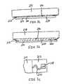
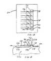
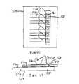
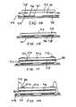
- One embodiment of the present inventionprovides a method of making a semiconductor chip package 10 having an expandable structure.
- a semiconductor chip 12 and a connection component 14 having electrically conductive partsare juxtaposed with one another before being bonded together to form a semiconductor chip package 10 .
- the semiconductor chip 12has a generally planer front face 16 including electrical parts or contacts 18 formed on peripheral regions of the front face 16 .
- Other types of semiconductor chipsmay also be used, such as chips having contacts disposed in an “area array”, i.e., an array covering substantially the entire front face of the chip with the contacts being uniformly spaced within the array.
- the contacts 18are arranged in rows (not shown) running substantially parallel to each edge of the chip 12 .
- connection component 14is preferably a flexible sheet, such as a flexible dielectric sheet comprising polymeric material, and has a first or bottom surface 20 , a second or top surface 22 and edges bounding the first surface 20 and the second surface 22 ; however, in other preferred embodiments the connection component 14 is desirably substantially rigid.
- the connection component 14also has a plurality of central terminals 24 distributed over the second surface 22 .
- the terminals 24are disposed at substantially even spaces on the second surface 22 so that the terminals 24 constitute an “area array.”
- the number of central terminals 24may be approximately equal to the number of peripheral contacts 18 on the semiconductor chip 12 . Nonetheless, the center-to-center linear distance between adjacent ones of the central terminals 24 is substantially greater than the center-to-center distance between adjacent peripheral contacts 18 on the chip 12 , because the central terminals 24 are substantially evenly distributed rather than concentrated in only a few rows.
- Each central terminal 24is connected with a partial lead 26 and a bonding terminal 28 , both of which are formed integrally with the central terminal 24 .
- the bonding terminals 28are arranged in rows adjacent the edges of the connection component 14 .
- the central terminals 24 , partial leads 26 and bonding terminals 28may be formed from substantially any electrically conductive material, but preferably are formed from metallic materials such as copper and copper alloys, noble metals and noble metal alloys.
- the central terminals 24provide for attachment of the semiconductor chip package 10 to a printed circuit board (“PCB”), typically by means of conventional solder balls or non collapsing (solid core) solder balls.
- PCBprinted circuit board
- the central terminals 24 , partial leads 26 and bonding terminalsare typically fabricated by conventional photolithographic, etching or deposition techniques.
- connection component 14is juxtaposed with the front face 16 of the chip 12 and an expandable structure 30 is disposed therebetween.
- the expandable structure 30will first be attached to the first surface 20 of the connection component 14 and the expandable structure/connection component subassembly will then be aligned with and assembled to a central portion of the front face 16 of the semiconductor chip 12 so that the expandable structure 30 does not cover the contacts 18 on the chip 12 .
- the expandable structure 30may comprise any number of materials which can be attached or uniformly applied to the connection component 14 and which can expand to occupy several times its original volume.
- one such expandable structure 30comprises a thermoplastic film loaded with a foaming agent; however, it is also contemplated that other expandable materials such as urethanes, olefinic thermoplastic elastomers and other elastomeric alloys.
- a conventional wire bonding machineis employed to bond the electrically conductive wires 32 between each chip contact 18 and a respective bonding terminal 28 on the second surface 22 of the connection component 14 . Utilization of the wire bonding machine preferably leaves sufficient slack in the wires 32 so that after expansion of the expandable structure 30 the wires 32 are not broken or stretched.
- the conductive wires 32are connected to the contacts 18 on the semiconductor chip 12 using a ball bond and the other ends of the conductive wires 32 are connected to the bonding terminals 28 using a wedge bond; however, other configurations can be used, e.g., wedge bonds at both ends of the conductive wire 32 .
- the wire bonding stepprecedes the step of expanding the expandable structure 30 so that the bonding terminals 28 are stationary and/or stable when the ends of the electrically conductive wires 32 are bonded thereto.
- stablemeans that the connection component and the expandable structure will absorb a minimal amount of the energy (e.g. ultrasonic energy) needed to insure a good bonding operation.
- the bonding terminals 28will remain essentially in one position during the bonding operation and will not move in either the vertical or the horizontal direction because, before the expanding step, the expandable structure 30 is substantially rigid. For example, if the bonding terminals 28 moved in the vertical direction during the bonding operation, then the positioning of the bonding wires 32 on the bonding terminals 28 would not be consistent and this may impede the formation of strong, reliable bonds.
- the expandable structure 30including the thermoplastic film and foaming agent, is exposed to sufficient heat so that the thermoplastic film will soften and the foaming agent will vaporize, thereby causing the thermoplastic film to foam and expand. Expansion of the expandable structure 30 causes the connection component 14 to move away from the chip 12 , as shown in FIG. 1 b .
- the expandable structure 30will be compliant or resilient after the expanding step.
- the wires 32 interconnecting the chip 12 to the connection component 14are provided with an expanding zone comprising excess slack to insure that the wires can flex and bend during the expanding step and so that the wires 32 are not stretched or pulled taut.
- platensmay be abutted against external surface regions of the semiconductor chip 12 and the connection component 14 .
- a first platen 52is abutted against the rear face 34 of the semiconductor chip 12 and a second platen 50 is abutted against a central region of the second surface 22 of the connection component 14 .
- the perimeter of the second platen 50is preferably bounded by the bonding terminals 28 so that the conductive wires 32 are not damaged.
- the expandable structure 30After the first and second platens 52 , 50 are in place, heat is applied to the expandable structure 30 and the expandable structure 30 is expanded in a controlled manner so that the connection component 14 moves away from the semiconductor chip 12 and so that the connection component 14 and the chip 12 are substantially parallel to one another.
- the overall thickness of the expandable structure 30may be controlled through use of the first and second platens 50 , 52 .
- the platensmay be pressed against the chip 12 and the connection component 14 to restrict expansion of the expandable structure during the expanding step.
- a dielectric encapsulantis allowed to flow between the connection component 14 and the semiconductor chip 12 and around the expandable structure 30 and the conductive wires 32 .
- Preferred dielectric encapsulantsmay include a liquid silicone rubber or other curable liquid elastomer.
- the encapsulant 36is cured using energy such as heat, ultraviolet light or other radiant energy to form a substantially uniform, planer, compliant layer between the semiconductor chip 12 and the connection component 14 . Because the encapsulant 36 is applied after the wire bonding operation, there is no risk of the encapsulant 36 coming in contact with the wires 32 or the electrically conductive parts of the chip 12 and the connection component 14 before the bonding step, which could diminish the strength of the bonds.
- connection component 114comprises a sheet-like dielectric film, and has a first surface 120 and a second surface 122 .
- the dielectric filmis preferably formed from a polymeric material of an approximate thickness between 25 microns and 75 microns.
- the connection component 114has conductive terminals 124 on its second surface 122 , electrical parts or leads 132 extending from the terminals 124 for electrically connecting the terminals 124 to contacts 118 on a semiconductor chip 112 , and bond windows for accessing the leads 132 while electrically connecting the leads 132 with the contacts 118 .
- the leads 132are typically lithographically defined on the dielectric film 114 to extend from the terminals 124 . Thus, in this particular embodiment, the leads 132 are only bonded to the contacts 118 on the semiconductor chip 112 and are not bonded to the dielectric film 114 .
- each terminal 124is connected with a contact 118 by bonding the leads 132 to the contacts 118 .
- the terminals 124 and leads 132may be formed from substantially any electrically conductive material 124 , but preferably are formed from metallic materials such as copper and copper alloys, noble metals and noble metal alloys and are typically fabricated by conventional photolithographic and etching or deposition techniques.
- the leads 132are electrically connected to the contacts 118 on the chip 112 by a conventional wire bonding operation, or by a bonding operation as shown in U.S. Pat. Nos.
- the expandable structure 130is subjected to heat so that the expandable structure expands as described above.
- the leads 132will bend and flex as the dielectric film 114 and the semiconductor chip 112 move away from one another; however, sufficient slack should remain in the leads 132 to account for thermal expansion differences between the semiconductor chip 112 and the dielectric film 114 .
- First and second platensmay be abutted against the dielectric film 114 and the chip 112 , respectively, to control expansion of the expandable structure 130 and to insure that the chip 112 and dielectric film 114 are substantially parallel to one another after the expanding step.
- the dielectric film 114is a flexible substrate.
- a first platenmay be abutted against the second surface 122 of the dielectric film 114 .
- the platenmay incorporate a vacuum to help insure that the dielectric film 114 is maintained parallel to the chip 112 during expansion of the expandable structure 130 .
- the dielectric 114 filmmay be maintained planar and parallel to the chip 112 by stretching the dielectric film 114 across a frame or a ring structure (not shown) prior to any of the above steps.
- a dielectric encapsulant 136is allowed to flow between the dielectric film 114 and the chip 112 and around the expandable structure 130 and the leads 132 while the chip 112 and dielectric film are compressed together or held in place.
- Preferred dielectric encapsulantsmay comprise a liquid silicone rubber or other curable liquid elastomer.
- a mask or coverlay 142may be placed over the bond windows 138 to prevent the encapsulant 136 from flowing through the bond windows 138 during the encapsulation process.
- the encapsulant 136is then cured by energy such as heat, ultraviolet light or other radiant energy to form a substantially uniform, planer, compliant layer between the chip 112 and the dielectric sheet 114 . Because the encapsulant 136 is applied after bonding, there is minimal risk of the encapsulant 136 coming in contact with the leads 132 or contacts 118 before bonding, which could diminish the strength of the bond
- FIGS. 3 a and 3 bshow a similar structure to that disclosed in FIGS. 2 a and 2 b ; however, the particular embodiment shown in FIGS. 3 a and 3 b comprise leads 232 which are connected to a first surface 220 of a dielectric film 214 , i.e., the non-exposed surface of the dielectric film 214 .
- a semiconductor chip 212 and the dielectric film 214are juxtaposed with one another and an expandable structure 230 is assembled between the front face 216 of the semiconductor chip 212 and the first surface 220 of the dielectric film 214 .
- the leads 232are then bonded to the contacts 218 on the front face 220 of the semiconductor chip 214 using a conventional bonding technique.
- each lead 232has an expansion section extending from an edge of the dielectric film 214 .
- the expansion sectionsare each bonded to a contact 218 on the semiconductor chip 212 .
- Each expansion sectionis laterally curved substantially parallel to the plane of the dielectric film 214 prior to the bonding operation.
- the expansion sectionslaterally curve at least twice in opposite directions (substantially “S” shaped) and may be curved more than twice.
- the laterally curved leads 232 extending 4 between the terminals on the dielectric film 214 and the contacts 218 on the chip 212create an expansion/contraction gap between the two microelectronic elements so that the expansion sections within the leads 232 may independently flex and bend during operational thermal cycling of the semiconductor chip package.
- leads 232 having lateral slack as shown in FIG. 3 cis described in greater detail in commonly assigned U.S. Pat. No. 5,821,608, the disclosure of which is hereby incorporated by reference herein.
- the lateral slack in the lead 232allows the lead 232 to expand in a somewhat spring-like manner as the expandable structure 230 is expanded.
- an encapsulant 236is allowed to flow between the dielectric film 214 and the semiconductor chip 212 and around the expandable structure 230 and the leads 232 , in accordance with the processes described above.
- an expandable structure 330is disposed between a substrate 314 , such as a printed circuit board or a rigid connection component, and the rear face 334 of a semiconductor chip 312 , i.e., the face of the semiconductor chip 312 opposite the front face 316 bearing contacts 318 .
- the expandable structure 330comprises a plurality or array of pads (i.e., a matrix of dots), whereby any two adjacent pads 330 define a channel 338 therebetween.
- the channels 338 running between adjacent padsare preferably between 75 to 100 microns wide, so that an encapsulant 336 , such as a curable silicone elastomer, may flow freely therethrough.
- the array of pads 330 shown in FIGS. 4 a and 4 bare described in greater detail in commonly assigned U.S. Pat. No. 5,659,952, the disclosure of which is hereby incorporated by reference herein.
- the array of pads 330are spaced close enough together so that adequate support is provided for maintaining substantial parallelism between the chip 312 and the substrate 314 .
- the pads 330should be far enough apart so that the channels 338 are sufficiently wide after the pads 330 have been expanded for allowing the encapsulant 336 to flow within the channels 338 .
- the pads 330comprise a thermoplastic film and a foaming agent. Upon application of a sufficient amount of heat, the thermoplastic film will soften and the foaming agent will vaporize, causing the array of pads 330 to expand to the configuration shown in FIG. 4 b .
- the semiconductor chip 312moves away from the substrate 314 .
- the semiconductor chip 312remains electrically interconnected to the substrate 314 because sufficient slack has been provided in the electrically conductive wires 332 .
- the pads 330are preferably compliant or resilient for responding to thermal cycling differences between the semiconductor chip 312 and the substrate 314 .
- the expandable structure 330may comprise a plurality of compliant pads connected by a web; a sheet having a plurality of compliant pads formed on opposite sides of the sheet; or a unitary structure having a square or rectangular shape.
- These various embodiments of the expandable structure 330can be used in processes as described above, and in other processes for fabricating connection components or microelectronic packages.
- the expandable structure according to the present inventionmay be stored and shipped with liner films applied to the surface regions thereof, as described in commonly assigned U.S. patent application Ser. No. 08/897,922, filed Jun. 20, 1997, the disclosure of which is hereby incorporated by reference herein.
- a dielectric encapsulantis allowed to flow between the substrate 314 and the rear face 334 of the semiconductor chip 312 and within the channels 338 .
- the encapsulant 336is a curable silicone elastomer such as the silicone elastomer 6811 manufactured by Dow Corning.
- the encapsulantmay comprise a compliant filler material, such as a liquid silicone rubber or other curable liquid elastomer. The encapsulant 336 material flows within the channels 338 running between the array of pads 330 while the semiconductor chip 312 and the substrate 314 are compressed together or held in place.
- the encapsulant 336is preferably substantially similar to the expandable material which forms the expandable structure 330 in order to provide a compliant interface having a more homogenous structure, thereby minimizing problems associated with thermal cycling. Further, the semiconductor chip package assembly is preferably entirely encapsulated with the encapsulant (not shown) so that the semiconductor chip 312 , electrically conductive wires 332 and substrate 314 are all covered by a second encapsulant.
- the first encapsulant and the second encapsulantmay comprise the same material and may be deposited at the same time.
- the encapsulant 336After the encapsulant 336 has been allowed to flow within the channels 338 between the chip 312 and around the conductive wires 332 , the encapsulant 336 is cured by using energy such as heat, ultraviolet light or other radiant energy to form a substantially uniform, planar compliant layer between the semiconductor chip 312 and the substrate 314 .
- energysuch as heat, ultraviolet light or other radiant energy
- FIGS. 5 a and 5 bA still further embodiment of the present invention is shown in FIGS. 5 a and 5 b .
- This particular embodimentincorporates a fan-out semiconductor chip package whereby the leads 432 are connected to respective contacts 418 on a semiconductor chip 412 and extend outwardly beyond the periphery of the chip 412 to terminals on a substrate 414 .
- a process in accordance with this particular embodiment of the present inventionutilizes a semiconductor chip 412 having a front face 416 with contacts 418 thereon and having an oppositely facing rear surface 434 .
- the particular chip illustrated in FIG. 5 ahas the contacts 418 disposed in an area array, i.e., an array covering substantially the entire front face 416 of the chip 412 , with the contacts 418 being uniformly spaced within the array.
- the chip 412is assembled in a package including a heat sink 440 .
- the heat sink 440is in the form of an open shell having a base wall 442 , side walls 444 projecting upwardly from the base wall 442 around the periphery thereof, and a projecting region 446 extending outwardly from the side walls 444 and defining a generally planer surface remote from the base wall.
- the rear face 434 of the semiconductor chip 412is bonded to the base wall 442 of the heat sink 440 by a thermally conductive adhesive layer.
- the adhesive layermay include any of the well known thermally conductive adhesive compositions, such as an epoxy loaded with metallic particles.
- the front face 416 of the chip 412is substantially coplanar with the projecting regions 446 of the heat sink 440 .
- the projecting regions 446 of the heat sink 440include a dielectric element 414 and an expandable structure 430 disposed between the dielectric element 414 and the projecting regions 446 of the heat sink 440 .
- the dielectric element 414includes a dielectric sheet incorporating one or more layers of a flexible, but substantially inextensible dielectric material. These flexible layers may include thin sheets of polyimide, typically having an aggregate thickness of about 25 microns (0.001 inch).
- the dielectric element 414has a top surface 422 , including electrically conductive terminals 424 which are distributed uniformly over the entire area of the top surface 422 , and a bottom surface 420 .
- the leads 432are bonded to the chip contacts 418 in accordance with processes described above and the expandable structure 430 is then expanded in a controlled manner as described above.
- the final assemblymay also be encapsulated using an encapsulant 436 as described above.
- a connection componentsuch as a flexible dielectric sheet 514 includes a bottom surface 520 , a top surface 522 and one or more bond windows 538 extending between the bottom and top surfaces.
- the flexible dielectric sheet 514includes a plurality of conductive leads 526 overlying the top surface 522 there.
- Each conductive lead 526preferably includes a terminal end 524 , a frangible end 528 remote therefrom, and v-shaped notches adjacent frangible end 528 .
- the v-shaped notches 527facilitate detachment of the frangible end 528 of lead 526 from the lead 526 .
- dielectric sheet 514is positioned atop a supporting substrate 552 having a top surface 554 and a support bar 556 projecting from the top surface thereof.
- the support bar 556is preferably sized and shaped to fit within bond window 538 .
- the dielectric sheet 514is positioned atop the first surface 554 of supporting substrate 552 so that the support bar 556 extends at least partially through bond window 538 .
- support bar 556provides support for the frangible end 528 of lead 526 so that the frangible end 528 does not break apart from lead 526 when the end of a wire is bonded thereto.
- the frangible end 528 of lead 526preferably overlies and is supported by support bar 556 .
- a wire bonding tool 558may then be used to dispensed conductive wires 532 having first ends 560 bonded to a main body portion of lead 526 and second ends 562 attached to the frangible ends 528 of the leads.
- FIGS. 6 c and 6 dafter the second ends 562 of conductive wires 532 have been attached to frangible ends 528 of leads 526 .
- the support barFIG. 6 b
- dielectric sheet 514is juxtaposed with a microelectronic element such as a semiconductor chip 512 .
- Semiconductor chip 512preferably includes a contact bearing face 516 , a rear surface 534 remote therefrom and one or more contacts 518 accessible at the contact bearing face.
- the dielectric sheet 514is preferably positioned atop the contact bearing face 516 of semiconductor chip 512 so that chip contacts 518 are in substantial alignment with bond window 538 .
- a bonding tool 558may then be utilized to bond the second end 562 of conductive wire 532 to the frangible end 528 of lead 526 , and for bonding the frangible end 528 of lead 526 to chip contact 518 .
- the dielectric sheet 514 and semiconductor chip 512are then moved away from one another.
- platensmay be temporarily attached to the connection component 514 and semiconductor chip 512 for controlling the movement of the dielectric sheet and semiconductor chip away from one another.
- the frangible ends 528 of leads 526break away from the main body portion of leads 526 at v-shaped notches 527 .
- conductive wire 532is drawn through the bond window 538 of dielectric sheet 514 , thereby removing at least some of the slack present in conductive wire 532 .
- slackgenerally means that the conductive wire is not stretched taut or tight.
- a curable liquid material 536such as a curable liquid elastomer may be introduced between dielectric sheet 514 and semiconductor chip 512 .
- the curable liquid materialmay be introduced either before, during or after the movement of dielectric sheet 514 and semiconductor chip 512 relative to one another.
- a coverlay(not shown) may be used to cover the bond windows 538 of dielectric sheet 514 so that the curable liquid material does not contact the top surface 522 of the dielectric sheet.
- the curable liquid material 536may be cured such as by using heat, light or other energy so as to provide a compliant or resilient layer between dielectric sheet 514 and semiconductor chip 512 .
- the complaint layer 536allows the dielectric sheet 514 and semiconductor chip 512 to move relative to one another during operation of the microelectronic assembly.
- conductive wire 532retains sufficient slack so that the conductive wire may flex and bend during thermal cycling for maintaining reliable electrical interconnections between the leads 526 of dielectric sheet 514 and the chip contacts 518 of semiconductor chip 512 .
- FIG. 7A-7Dshow a method of making a microelectronic assembly in accordance with other preferred embodiments of the present invention.
- a connection componentsuch as dielectric sheet 614 includes a bottom surface 620 , a top surface 622 and a plurality of conductive leads 626 formed over the top surface 622 .
- Each conductive lead 626preferably includes a terminal end 624 and at least one bond window 638 remote from the terminal end 624 .
- Bond window 638is desirably elongated and extends in a direction transverse to the longitudinal direction of conductive leads 626 .
- Each dielectric sheet 614also desirably includes a conductive pad 628 associated with one of the conductive leads 626 . In the particular embodiment shown in FIG. 7A , each conductive pad 628 is in substantial alignment with one of the conductive leads 626 .
- dielectric sheet 614is placed atop a supporting substrate 652 so that the bottom surface 620 of dielectric sheet 614 abuts against a top surface 654 of the supporting substrate.
- a wire bonding tool(not shown) is then used to attach first ends 660 of conductive wires 632 to leads 626 and second ends 662 of the conductive wires to conductive pads 628 .
- the dielectric sheet 614is preferably positioned atop a semiconductor chip 612 having a contact bearing face 616 with one or more chip contacts 618 .
- Dielectric sheet 614is desirably positioned atop the contact bearing face 616 of chip 612 so that the bond window 638 of dielectric sheet 614 is in substantial alignment with the chip contact 618 .
- a bonding tool 658may then be utilized to break the conductive wire 632 adjacent the second end 662 attached to conductive pad 628 . The bonding tool 658 effectively detaches the second end of the conductive wire 632 and bonds the second end to chip contact 618 .
- a first platen 680may be secured over the back surface 634 of semiconductor chip 652 .
- a second platen 682may be secured over the first surface 622 of dielectric sheet 614 .
- a vacuummay then be activated through the first and second platens 680 , 682 so that the dielectric sheet 614 and semiconductor chip 652 may be moved away from one another in a controlled manner.
- the conductive wire 632is drawn through bond window 638 .
- the conductive wirebends and flexes so that at least some of the slack is removed from wire 632 .
- the displacement of dielectric sheet 614 and semiconductor chip 652is limited so that sufficient slack remains in the conductive wire 632 after the moving step.
- a curable liquid material 636such as a curable liquid elastomer, may be introduced between the dielectric sheet 614 and the semiconductor chip 652 .
- the curable liquid material 636may be introduced either before, during or after the moving step.
- One or more cover layersmay be placed atop either the dielectric sheet or the semiconductor chip so as to prevent the curable liquid encapsulant engaging electrically conductive parts in embodiments where such engagement is undesirable.
- a cover layermay be placed atop the first surface 622 of dielectric sheet 614 so as to prevent the curable liquid encapsulant from contacting selected portions of conductive lead 626 .
- the curable liquid materialis preferably cured to form a compliant layer 636 that allows dielectric sheet 614 and chip 652 to move relative to one another during thermal cycling.
- the compliant layeralso enables conductive wire 632 to flex and bend during thermal cycling so as to maintain the electrical interconnection between lead 626 and chip contact 618 .
- dielectric sheet 714has a bottom surface 720 , a top surface 722 , and one or more conductive leads 726 formed on top surface 722 .
- Each conductive leadpreferably extends toward a bond window 738 .
- the bond windowmay be elongated.
- Each conductive lead 726has a conductive wire 732 having a first end 760 bonded to conductive lead 726 and a second end 762 that extends over the top surface 722 of dielectric sheet 714 .
- Dielectric sheet 714is preferably juxtaposed with a microelectronic element such as semiconductor chip 752 having a contact bearing surface 716 with one or more chip contacts 718 and a back surface 734 remote therefrom.
- the bond window 738 of dielectric sheet 714is preferably aligned with the one or more chip contacts 718 so that the second ends 762 of conductive wires 732 overly the chip contacts 718 .
- a wire bonding tool 758is then utilized to bond the second ends 762 of conductive wires 732 to chip contacts 718 .
- the dielectric sheet and semiconductor chipare preferably moved away from one another in a controlled manner so that at least one conductive wire 732 is drawn through bond window 738 of dielectric sheet.
- chip 752 and dielectric sheet 714move away from one another, at least some of the slack in conductive wire 732 is removed, whereby the conductive wire is bent in a downward direction toward the bottom surface 720 of dielectric sheet 714 .
- a curable liquid material 736may be introduced between the dielectric sheet 714 and semiconductor chip 752 .
- one or more cover layersmay be applied over the exterior surfaces of the dielectric sheet 714 and/or semiconductor chip 752 so as to control the flow of the curable liquid material 736 when such material is in an uncured state.
- Energysuch as light or heat, may be applied to the curable liquid material 736 so as to provide a dielectric layer between dielectric sheet 714 and semiconductor chip 752 and around at least a portion of conductive wire 732 .
- the dielectric layeris a compliant layer that allows dielectric sheet 714 and semiconductor chip 752 to move relative to one another during thermal cycling.
- Compliant layer 736also allows conductive wire 732 to flex and bend during operation of the microelectronic assembly so as to maintain a reliable electrical interconnection between conductive lead 726 and chip contact 718 .
- a flexible connection componentsuch as dielectric sheet 814 includes a top surface 822 and a bottom surface 820 having a plurality of conductive leads 826 formed thereon.
- Each conductive lead 826preferably includes a terminal end 824 that overlies the bottom surface 820 of dielectric sheet 814 and tip ends 828 that extend into bond window 838 .
- the dielectric sheet 814is preferably juxtaposed with a microelectronic element such as a semiconductor chip 812 having a contact bearing face 816 and a rear surface 834 remote therefrom.
- the contact bearing face 816 of microelectronic element 812includes one or more insulating pads 890 attached to the contact bearing face 816 . In the particular embodiment shown in FIG. 9A , the insulating pads 890 surround one or more contacts 818 accessible at the contact bearing face 816 .
- the bond window 838 of dielectric sheet 814is placed in substantial alignment with the chip contacts 818 and insulating pads 890 of chips 812 , and tip ends 828 of conductive leads 826 are preferably abutted against insulating pads 890 .
- the tip ends 828 of leads 826engage the insulating pads while a gap 892 is formed between the remainder of lead 826 and contact bearing face 816 of microelectronic element 812 .
- the chip contacts 818are preferably accessible through bond window 838 .
- a wire bonding toolmay be used to electrically interconnect the tip ends 828 of leads 826 and the chip contacts 818 .
- Each bonded conductive wire 832preferably has a first end 860 bonded to a tip end 828 of lead 826 and a second end 862 bonded to a chip contact 818 .
- a first platen 880may be positioned over the rear surface 834 of microelectronic element 812 and a second platen 882 may be provided over the top surface 822 of dielectric sheet 814 .
- a vacuummay be activated through the first and second platens 880 , 882 and the platens moved away from one another in a controlled manner so that dielectric sheet 814 and microelectronic element 812 move away from one another.
- the conductive wires 632bend into the extended orientation shown in FIG. 9 D. Because the second ends 862 of the conductive wires are bonded to the tip ends 828 of leads 826 , the tip ends 828 of leads 826 also flex slightly in a downward direction toward the contact bearing surface 816 of microelectronic element 812 .
- a curable liquid material 836may be introduced between dielectric sheet 814 and microelectronic element 812 .
- the curable liquid materialmay be introduced either before, during or after the moving step.
- the curable liquid materialmay then be cured, such as by using heat or light, so as to provide a compliant layer between dielectric sheet 814 and microelectronic element 812 .
- the compliant layer 836allows the components to move relative to one another during thermal cycling of the microelectronic assembly.
- the compliant layer 836also allows the conductive wires 832 and leads 826 to flex as necessary so as to maintain a reliable electrical interconnection between chip contacts 818 and leads 826 .
- FIG. 9D-1shows a plan view of the assembly shown in FIG. 9 D.
- the assemblyincludes dielectric sheet 814 overlying contact bearing face 816 of microelectronic element 812 .
- the contact bearing face 816includes a plurality of chip contacts 818 that are in substantial alignment with the bond window 838 of dielectric sheet 814 .
- Dielectric sheet 814includes a plurality of conductive leads 826 extending along an underside surface thereof. Each lead includes a tip end 828 that projects into bond window 838 . After dielectric sheet 814 is placed atop microelectronic element 812 , the tip ends 828 of conductive leads 826 are preferably in substantial alignment with the chip contacts 818 .
- Conductive wires 832electrically interconnect each chip contact 818 with one of the conductive leads 826 .
- a microelectronic assemblyincludes a connection component 914 such as a dielectric sheet 914 having a first surface 922 and a second surface 920 remote therefrom.
- the dielectric sheet 914preferably includes a plurality of flexible, conductive leads 926 having terminal ends 924 permanently attached to dielectric sheet 914 and tip ends 928 releasably attached to dielectric sheet 914 .
- Releasable leadsare disclosed in certain preferred embodiments of commonly assigned U.S. Pat. Nos. 5,763,941 and 5,904,498, and U.S. patent application Ser. Nos. 09/020,750 filed Feb. 9, 1998, Ser. No. 09/195,371 filed Nov. 18, 1998, Ser. No.
- the first surface 922 of dielectric sheet 914also preferably includes one or more connection component contacts 970 .
- the assemblyalso desirably includes a first microelectronic element 912 having a contact bearing face 916 with a plurality of contacts 918 .
- the first microelectronic element 912is abutted against the dielectric sheet 914 so that the contacts 918 engage the tip ends 928 of leads 926 .
- the tip ends 928may be secured to the contacts 918 using bonding techniques such as diffusion bonding, thermosonic bonding and solder reflow bonding techniques.
- a conductive adhesive(not shown) may be provided between the contacts 918 and the tip ends 928 so as to adhere the contacts 918 to the tip ends 928 .
- a second microelectronic element 972 having a contact bearing face 974 including contacts 976 and a rear surface 978 remote therefrommay be juxtaposed with the back surface 934 of the first microelectronic element 912 .
- An adhesive 980such as a thermally conductive adhesive, may be provided between the opposing rear surfaces 934 , 978 of the first and second microelectronic elements 912 , 972 .
- a wire bonding tool(not shown) may be utilized so as to electrically interconnect chip contacts 976 of the second microelectronic element 972 with the connection component contacts 970 of dielectric sheet 914 .
- Each conductive wire 932preferably has a first end 960 bonded to one of the chip contacts 976 of the second microelectronic element 972 and a second end 962 bonded to a dielectric sheet contact 970 .
- the first and second microelectronic elements 972 , 912are moved away from dielectric sheet 914 in a controlled manner.
- the tip ends 928 of flexible leads 926are released from the top surface 922 of dielectric sheet 914 .
- the conductive leads 926are bent into the substantially s-shaped configuration shown in FIG. 10 e , thereby enabling the leads to flex and bend during operation of the assembly.
- the conductive wires 932also flex and bend to account for the increased distance between the contacts 976 of second microelectronic element 972 and the connection component contacts 970 .
- the conductive wires 932maintain a sufficient amount of slack so that the first and second microelectronic elements 912 , 972 may move relative to the dielectric sheet 914 while maintaining a reliable electrical interconnection between contacts 976 and connection component contacts 970 .
- a curable liquid material 936may be provided between the top surface 922 of dielectric sheet 914 and the contact bearing face 916 of first microelectronic element 912 .
- the encapsulant material 936is also preferably provided around the first and second microelectronic elements 912 , 972 , the contacts 976 of the second microelectronic 972 , and the conductive wires 932 .
- the curable liquid material 936is preferably cured such as by using heat or light so as to provide a compliant layer that enables the first and second microelectronic elements 912 , 972 to move relative to the dielectric sheet 914 during thermal cycling of the microelectronic assembly.
- the compliant layer 936also allows the conductive wires 932 and flexible leads 926 to flex and bend during thermal cycling while maintaining a reliable electrical interconnection between various components of the assembly.
- one or more conductive massessuch as solder balls 998 may be attached to terminals (not shown) accessible at the bottom surface 920 of dielectric sheet 914 .
- viasmay be formed in dielectric sheet 914 to provide access to the connection component contacts 970 so that the conductive masses 998 may be electrically interconnected with the dielectric sheet contacts 970 or leads 926 .
- a first set of solder balls 998 care electrically interconnected with the terminal ends 924 of conductive leads 926
- a second set of solder balls 998 aare electrically interconnected with the connection component contacts 970 .
- solder balls 998may be connected to the contacts of an external element such as a printed circuit board or circuitized substrate.
- one or more of the terminal ends 924 of leads 926may be electrically interconnected with one or more of the contacts 970 of the dielectric sheet 914 via an electrically conductive trace extending therebetween.
- a single solder ball 998 Cmay electrically interconnect a contact of the first microelectronic element 912 with a contact of the second microelectronic element.
- a microelectronic assembly including conductive wires 1032may be placed in a mold 1071 having an upper member 1073 with one or more recesses 1075 and a lower member 1077 .
- the assemblyis placed in mold 1071 .
- the microelectronic element 1012desirably sits within the lower mold member 1077 and the upper mold member 1073 is placed atop the lower mold member 1077 .
- the recess 1075 of the upper mold member 1073is preferably placed in alignment over a looped portion of the conductive wire 1032 .
- a curable liquid material 1036is introduced into mold 1071 , the curable liquid material passes between dielectric sheet 1014 and microelectronic element 1012 .
- the curable liquid material 1036also passes through the bond window 1038 of dielectric sheet 1014 and into the recess 1075 of upper mold member 1073 .
- the curable liquid materialencapsulates the portion of the conductive wire 1032 therein.
- the curable liquid material 1036is preferably cured to provide a compliant layer that allows the dielectric sheet and microelectronic element to move relative to one another during operation of the microelectronic assembly.
- the microelectronic assemblymay be removed from the mold.
- the microelectronic assemblyincludes dielectric sheet 1014 electrically interconnected with microelectronic element 1012 by one or more conductive wires 1032 .
- a projecting portion 1079 of the compliant layer 1036projects above the top surface 1022 of dielectric sheet 1014 .
- the projecting portion 1079encapsulates the portion of the conductive wire 1032 projecting through bond window 1038 and above the top surface 1022 of dielectric sheet 1014 .
- the foaming agent for expanding the substratemay be a chemically reactive material.
- many microelectronic packagesmay be simultaneously manufactured using the processes described above. These packages are then separated from one another using a standard dicing technique and the individual microelectronic packages may be attached to a supporting substrate such as a standard printed circuit board. Accordingly, the foregoing description of the preferred embodiments should be taken by way of illustration rather than by way of limitation of the invention.
Landscapes
- Engineering & Computer Science (AREA)
- Power Engineering (AREA)
- Microelectronics & Electronic Packaging (AREA)
- Computer Hardware Design (AREA)
- Physics & Mathematics (AREA)
- Condensed Matter Physics & Semiconductors (AREA)
- General Physics & Mathematics (AREA)
- Manufacturing & Machinery (AREA)
- Wire Bonding (AREA)
Abstract
Description
Claims (22)
Priority Applications (2)
| Application Number | Priority Date | Filing Date | Title |
|---|---|---|---|
| US09/766,814US6848173B2 (en) | 1994-07-07 | 2001-01-22 | Microelectric packages having deformed bonded leads and methods therefor |
| US11/043,354US20050155223A1 (en) | 1994-07-07 | 2005-01-26 | Methods of making microelectronic assemblies |
Applications Claiming Priority (12)
| Application Number | Priority Date | Filing Date | Title |
|---|---|---|---|
| US08/271,768US5518964A (en) | 1994-07-07 | 1994-07-07 | Microelectronic mounting with multiple lead deformation and bonding |
| US08/440,665US5801441A (en) | 1994-07-07 | 1995-05-15 | Microelectronic mounting with multiple lead deformation and bonding |
| US361995P | 1995-09-12 | 1995-09-12 | |
| US08/678,808US5830782A (en) | 1994-07-07 | 1996-07-12 | Microelectronic element bonding with deformation of leads in rows |
| US08/712,855US6191368B1 (en) | 1995-09-12 | 1996-09-12 | Flexible, releasable strip leads |
| US3287096P | 1996-12-13 | 1996-12-13 | |
| US98809797A | 1997-12-10 | 1997-12-10 | |
| US09/057,125US5959354A (en) | 1994-07-07 | 1998-04-08 | Connection components with rows of lead bond sections |
| US09/138,858US6104087A (en) | 1994-07-07 | 1998-08-24 | Microelectronic assemblies with multiple leads |
| US09/271,688US6429112B1 (en) | 1994-07-07 | 1999-03-18 | Multi-layer substrates and fabrication processes |
| US09/520,320US6486003B1 (en) | 1996-12-13 | 2000-03-07 | Expandable interposer for a microelectronic package and method therefor |
| US09/766,814US6848173B2 (en) | 1994-07-07 | 2001-01-22 | Microelectric packages having deformed bonded leads and methods therefor |
Related Parent Applications (3)
| Application Number | Title | Priority Date | Filing Date |
|---|---|---|---|
| US09/138,858Continuation-In-PartUS6104087A (en) | 1994-07-07 | 1998-08-24 | Microelectronic assemblies with multiple leads |
| US09/271,688Continuation-In-PartUS6429112B1 (en) | 1994-07-07 | 1999-03-18 | Multi-layer substrates and fabrication processes |
| US09/520,320Continuation-In-PartUS6486003B1 (en) | 1994-07-07 | 2000-03-07 | Expandable interposer for a microelectronic package and method therefor |
Related Child Applications (2)
| Application Number | Title | Priority Date | Filing Date |
|---|---|---|---|
| US09/520,320ContinuationUS6486003B1 (en) | 1994-07-07 | 2000-03-07 | Expandable interposer for a microelectronic package and method therefor |
| US11/043,354DivisionUS20050155223A1 (en) | 1994-07-07 | 2005-01-26 | Methods of making microelectronic assemblies |
Publications (2)
| Publication Number | Publication Date |
|---|---|
| US20020068426A1 US20020068426A1 (en) | 2002-06-06 |
| US6848173B2true US6848173B2 (en) | 2005-02-01 |
Family
ID=34109348
Family Applications (2)
| Application Number | Title | Priority Date | Filing Date |
|---|---|---|---|
| US09/766,814Expired - Fee RelatedUS6848173B2 (en) | 1994-07-07 | 2001-01-22 | Microelectric packages having deformed bonded leads and methods therefor |
| US11/043,354AbandonedUS20050155223A1 (en) | 1994-07-07 | 2005-01-26 | Methods of making microelectronic assemblies |
Family Applications After (1)
| Application Number | Title | Priority Date | Filing Date |
|---|---|---|---|
| US11/043,354AbandonedUS20050155223A1 (en) | 1994-07-07 | 2005-01-26 | Methods of making microelectronic assemblies |
Country Status (1)
| Country | Link |
|---|---|
| US (2) | US6848173B2 (en) |
Cited By (31)
| Publication number | Priority date | Publication date | Assignee | Title |
|---|---|---|---|---|
| US20040191958A1 (en)* | 2002-12-30 | 2004-09-30 | Infineon Technologies Ag | Method for connecting an integrated circuit to a substrate and corresponding arrangement |
| US20040252477A1 (en)* | 2003-06-11 | 2004-12-16 | Brown Dirk D. | Contact grid array formed on a printed circuit board |
| US20050120553A1 (en)* | 2003-12-08 | 2005-06-09 | Brown Dirk D. | Method for forming MEMS grid array connector |
| US20050124181A1 (en)* | 2003-12-08 | 2005-06-09 | Brown Dirk D. | Connector for making electrical contact at semiconductor scales |
| US20050164527A1 (en)* | 2003-04-11 | 2005-07-28 | Radza Eric M. | Method and system for batch forming spring elements in three dimensions |
| US20050208787A1 (en)* | 2004-03-19 | 2005-09-22 | Epic Technology Inc. | Interposer with compliant pins |
| US20050208788A1 (en)* | 2004-03-19 | 2005-09-22 | Dittmann Larry E | Electrical connector in a flexible host |
| US20050205988A1 (en)* | 2004-03-19 | 2005-09-22 | Epic Technology Inc. | Die package with higher useable die contact pad area |
| US20050208786A1 (en)* | 2004-03-19 | 2005-09-22 | Epic Technology Inc. | Interposer and method for making same |
| US20050227510A1 (en)* | 2004-04-09 | 2005-10-13 | Brown Dirk D | Small array contact with precision working range |
| US20060000642A1 (en)* | 2004-07-01 | 2006-01-05 | Epic Technology Inc. | Interposer with compliant pins |
| US7056131B1 (en) | 2003-04-11 | 2006-06-06 | Neoconix, Inc. | Contact grid array system |
| US20060258183A1 (en)* | 2003-04-11 | 2006-11-16 | Neoconix, Inc. | Electrical connector on a flexible carrier |
| US20060258182A1 (en)* | 2004-07-20 | 2006-11-16 | Dittmann Larry E | Interposer with compliant pins |
| US20070054515A1 (en)* | 2003-04-11 | 2007-03-08 | Williams John D | Method for fabricating a contact grid array |
| US20070134949A1 (en)* | 2005-12-12 | 2007-06-14 | Dittmann Larry E | Connector having staggered contact architecture for enhanced working range |
| US20070141863A1 (en)* | 2003-04-11 | 2007-06-21 | Williams John D | Contact grid array system |
| US20070164412A1 (en)* | 2002-10-15 | 2007-07-19 | Megica Corporation | Method of wire bonding over active area of a semiconductor circuit |
| US20070218710A1 (en)* | 2003-06-11 | 2007-09-20 | Brown Dirk D | Structure and process for a contact grid array formed in a circuitized substrate |
| US20070232053A1 (en)* | 2002-10-24 | 2007-10-04 | Megica Corporation | Method for fabricating thermal compliant semiconductor chip wiring structure for chip scale packaging |
| US20070259539A1 (en)* | 2003-04-11 | 2007-11-08 | Brown Dirk D | Method and system for batch manufacturing of spring elements |
| US7347698B2 (en) | 2004-03-19 | 2008-03-25 | Neoconix, Inc. | Deep drawn electrical contacts and method for making |
| US20080142965A1 (en)* | 2006-12-18 | 2008-06-19 | Advanced Connection Technology Inc. | Chip package |
| US20080284003A1 (en)* | 2007-05-17 | 2008-11-20 | Chua Swee Kwang | Semiconductor Packages And Method For Fabricating Semiconductor Packages With Discrete Components |
| US20090057919A1 (en)* | 2000-05-19 | 2009-03-05 | Megica Corporation | Multiple chips bonded to packaging structure with low noise and multiple selectable functions |
| US20100167561A1 (en)* | 2003-04-11 | 2010-07-01 | Neoconix, Inc. | Structure and process for a contact grid array formed in a circuitized substrate |
| US8168527B2 (en) | 2006-09-06 | 2012-05-01 | Megica Corporation | Semiconductor chip and method for fabricating the same |
| US8426982B2 (en) | 2001-03-30 | 2013-04-23 | Megica Corporation | Structure and manufacturing method of chip scale package |
| US8641428B2 (en) | 2011-12-02 | 2014-02-04 | Neoconix, Inc. | Electrical connector and method of making it |
| US9680273B2 (en) | 2013-03-15 | 2017-06-13 | Neoconix, Inc | Electrical connector with electrical contacts protected by a layer of compressible material and method of making it |
| US20220375891A1 (en)* | 2011-05-03 | 2022-11-24 | Tessera Llc | Package-on-package assembly with wire bonds to encapsulation surface |
Families Citing this family (6)
| Publication number | Priority date | Publication date | Assignee | Title |
|---|---|---|---|---|
| US6249135B1 (en)* | 1997-09-19 | 2001-06-19 | Fujitsu Limited | Method and apparatus for passive optical characterization of semiconductor substrates subjected to high energy (MEV) ion implantation using high-injection surface photovoltage |
| US20090260862A1 (en)* | 2008-04-16 | 2009-10-22 | Andrew Yaung | Circuit modification device for printed circuit boards |
| DE102010010721A1 (en)* | 2010-03-09 | 2011-09-15 | Oliver Kömmerling | Method for generating connection between computer chip and electric guard, for electronic component testing circuitry to e.g. analyze error, involves creating connection between end and circuitry portion by joining process |
| KR20160006494A (en)* | 2014-07-09 | 2016-01-19 | 삼성전자주식회사 | Capacitive micromachined ultrasonic transducer probe using wire-bonding |
| US9543277B1 (en)* | 2015-08-20 | 2017-01-10 | Invensas Corporation | Wafer level packages with mechanically decoupled fan-in and fan-out areas |
| US10429321B2 (en) | 2016-08-29 | 2019-10-01 | Kla-Tencor Corporation | Apparatus for high-speed imaging sensor data transfer |
Citations (42)
| Publication number | Priority date | Publication date | Assignee | Title |
|---|---|---|---|---|
| US3577037A (en) | 1968-07-05 | 1971-05-04 | Ibm | Diffused electrical connector apparatus and method of making same |
| US3811186A (en) | 1972-12-11 | 1974-05-21 | Ibm | Method of aligning and attaching circuit devices on a substrate |
| US3921285A (en) | 1974-07-15 | 1975-11-25 | Ibm | Method for joining microminiature components to a carrying structure |
| US4535219A (en) | 1982-10-12 | 1985-08-13 | Xerox Corporation | Interfacial blister bonding for microinterconnections |
| US4545610A (en) | 1983-11-25 | 1985-10-08 | International Business Machines Corporation | Method for forming elongated solder connections between a semiconductor device and a supporting substrate |
| US4764848A (en) | 1986-11-24 | 1988-08-16 | International Business Machines Corporation | Surface mounted array strain relief device |
| US4878611A (en) | 1986-05-30 | 1989-11-07 | American Telephone And Telegraph Company, At&T Bell Laboratories | Process for controlling solder joint geometry when surface mounting a leadless integrated circuit package on a substrate |
| US4893172A (en) | 1987-01-19 | 1990-01-09 | Hitachi, Ltd. | Connecting structure for electronic part and method of manufacturing the same |
| JPH0220032A (en)* | 1988-07-08 | 1990-01-23 | Seikosha Co Ltd | Sealing method for resin of semiconductor element |
| US5067007A (en) | 1988-06-13 | 1991-11-19 | Hitachi, Ltd. | Semiconductor device having leads for mounting to a surface of a printed circuit board |
| US5086337A (en) | 1987-01-19 | 1992-02-04 | Hitachi, Ltd. | Connecting structure of electronic part and electronic device using the structure |
| US5148266A (en) | 1990-09-24 | 1992-09-15 | Ist Associates, Inc. | Semiconductor chip assemblies having interposer and flexible lead |
| US5148265A (en)* | 1990-09-24 | 1992-09-15 | Ist Associates, Inc. | Semiconductor chip assemblies with fan-in leads |
| US5152695A (en) | 1991-10-10 | 1992-10-06 | Amp Incorporated | Surface mount electrical connector |
| US5173055A (en) | 1991-08-08 | 1992-12-22 | Amp Incorporated | Area array connector |
| US5189507A (en) | 1986-12-17 | 1993-02-23 | Raychem Corporation | Interconnection of electronic components |
| US5282312A (en) | 1991-12-31 | 1994-02-01 | Tessera, Inc. | Multi-layer circuit construction methods with customization features |
| US5296737A (en)* | 1990-09-06 | 1994-03-22 | Hitachi, Ltd. | Semiconductor device with a plurality of face to face chips |
| US5367764A (en) | 1991-12-31 | 1994-11-29 | Tessera, Inc. | Method of making a multi-layer circuit assembly |
| US5385291A (en) | 1994-01-10 | 1995-01-31 | Micron Custom Manufacturing Services, Inc. | Method employing an elevating of atmospheric pressure during the heating and/or cooling phases of ball grid array (BGA) soldering of an IC device to a PCB |
| US5390844A (en) | 1993-07-23 | 1995-02-21 | Tessera, Inc. | Semiconductor inner lead bonding tool |
| US5398863A (en) | 1993-07-23 | 1995-03-21 | Tessera, Inc. | Shaped lead structure and method |
| US5491302A (en) | 1994-09-19 | 1996-02-13 | Tessera, Inc. | Microelectronic bonding with lead motion |
| US5518964A (en) | 1994-07-07 | 1996-05-21 | Tessera, Inc. | Microelectronic mounting with multiple lead deformation and bonding |
| US5536909A (en) | 1992-07-24 | 1996-07-16 | Tessera, Inc. | Semiconductor connection components and methods with releasable lead support |
| US5587341A (en) | 1987-06-24 | 1996-12-24 | Hitachi, Ltd. | Process for manufacturing a stacked integrated circuit package |
| WO1997011588A1 (en) | 1995-09-18 | 1997-03-27 | Tessera, Inc. | Microelectronic lead structures with dielectric layers |
| US5620928A (en)* | 1995-05-11 | 1997-04-15 | National Semiconductor Corporation | Ultra thin ball grid array using a flex tape or printed wiring board substrate and method |
| US5637925A (en)* | 1988-02-05 | 1997-06-10 | Raychem Ltd | Uses of uniaxially electrically conductive articles |
| US5659952A (en)* | 1994-09-20 | 1997-08-26 | Tessera, Inc. | Method of fabricating compliant interface for semiconductor chip |
| US5684677A (en) | 1993-06-24 | 1997-11-04 | Kabushiki Kaisha Toshiba | Electronic circuit device |
| US5726500A (en) | 1994-04-08 | 1998-03-10 | Thomson-Csf | Semiconductor hybrid component |
| US5739053A (en) | 1992-10-27 | 1998-04-14 | Matsushita Electric Industrial Co., Ltd. | Process for bonding a semiconductor to a circuit substrate including a solder bump transferring step |
| US5763941A (en) | 1995-10-24 | 1998-06-09 | Tessera, Inc. | Connection component with releasable leads |
| US5777386A (en) | 1995-08-23 | 1998-07-07 | Shinko Electric Industries Co., Ltd. | Semiconductor device and mount structure thereof |
| US5794330A (en) | 1994-02-01 | 1998-08-18 | Tessera, Inc. | Microelectronics unit mounting with multiple lead bonding |
| WO1998044564A1 (en) | 1997-04-02 | 1998-10-08 | Tessera, Inc. | Chip with internal signal routing in external element |
| US5830782A (en) | 1994-07-07 | 1998-11-03 | Tessera, Inc. | Microelectronic element bonding with deformation of leads in rows |
| US5859472A (en) | 1996-09-12 | 1999-01-12 | Tessera, Inc. | Curved lead configurations |
| US5898223A (en) | 1997-10-08 | 1999-04-27 | Lucent Technologies Inc. | Chip-on-chip IC packages |
| US6016013A (en) | 1996-08-20 | 2000-01-18 | Nec Corporation | Semiconductor device mounting structure |
| US6057598A (en) | 1997-01-31 | 2000-05-02 | Vlsi Technology, Inc. | Face on face flip chip integration |
Family Cites Families (70)
| Publication number | Priority date | Publication date | Assignee | Title |
|---|---|---|---|---|
| US406704A (en)* | 1889-07-09 | Thermostatic draft-regulator | ||
| GB1015909A (en)* | 1963-12-30 | 1966-01-05 | Gen Micro Electronics Inc | Method of and product for packaging electronic devices |
| US3342189A (en)* | 1964-06-04 | 1967-09-19 | Loretta M Houston | Elevated wig for forming an enlarged hairdo |
| US3376326A (en)* | 1964-12-31 | 1968-04-02 | Procter & Gamble | Interesterification of glycerides |
| US3373481A (en)* | 1965-06-22 | 1968-03-19 | Sperry Rand Corp | Method of electrically interconnecting conductors |
| DE2119567C2 (en)* | 1970-05-05 | 1983-07-14 | International Computers Ltd., London | Electrical connection device and method for making the same |
| CA954635A (en)* | 1972-06-06 | 1974-09-10 | Microsystems International Limited | Mounting leads and method of fabrication |
| US3952404A (en)* | 1973-07-30 | 1976-04-27 | Sharp Kabushiki Kaisha | Beam lead formation method |
| DE2608250C3 (en)* | 1976-02-28 | 1985-06-05 | Telefunken electronic GmbH, 7100 Heilbronn | Method for thermocompression joining of metal connection contacts located on semiconductor bodies with associated housing connection parts and device for carrying out the method |
| US4037270A (en)* | 1976-05-24 | 1977-07-19 | Control Data Corporation | Circuit packaging and cooling |
| US4067104A (en)* | 1977-02-24 | 1978-01-10 | Rockwell International Corporation | Method of fabricating an array of flexible metallic interconnects for coupling microelectronics components |
| US4326663A (en)* | 1978-07-20 | 1982-04-27 | Eltec Instruments, Inc. | Pyroelectric detector |
| JPS5555985U (en)* | 1978-10-12 | 1980-04-16 | ||
| JPS6038809B2 (en)* | 1979-11-20 | 1985-09-03 | 信越ポリマ−株式会社 | Method for manufacturing elastic structure with anisotropic conductivity |
| US5286811A (en)* | 1983-09-27 | 1994-02-15 | The Boeing Company | Blended polyimide oligomers and method of curing polyimides |
| US4447857A (en)* | 1981-12-09 | 1984-05-08 | International Business Machines Corporation | Substrate with multiple type connections |
| US4563725A (en)* | 1983-01-06 | 1986-01-07 | Welwyn Electronics Limited | Electrical assembly |
| US4751199A (en)* | 1983-12-06 | 1988-06-14 | Fairchild Semiconductor Corporation | Process of forming a compliant lead frame for array-type semiconductor packages |
| US4667219A (en)* | 1984-04-27 | 1987-05-19 | Trilogy Computer Development Partners, Ltd. | Semiconductor chip interface |
| JPS61111561A (en)* | 1984-10-05 | 1986-05-29 | Fujitsu Ltd | semiconductor equipment |
| US4661192A (en)* | 1985-08-22 | 1987-04-28 | Motorola, Inc. | Low cost integrated circuit bonding process |
| US5917707A (en)* | 1993-11-16 | 1999-06-29 | Formfactor, Inc. | Flexible contact structure with an electrically conductive shell |
| US4766670A (en)* | 1987-02-02 | 1988-08-30 | International Business Machines Corporation | Full panel electronic packaging structure and method of making same |
| US4918571A (en)* | 1987-03-31 | 1990-04-17 | Amp Incorporated | Chip carrier with energy storage means |
| US4812191A (en)* | 1987-06-01 | 1989-03-14 | Digital Equipment Corporation | Method of forming a multilevel interconnection device |
| JP2641869B2 (en)* | 1987-07-24 | 1997-08-20 | 三菱電機株式会社 | Method for manufacturing semiconductor device |
| US5230931A (en)* | 1987-08-10 | 1993-07-27 | Semiconductor Energy Laboratory Co., Ltd. | Plasma-assisted cvd of carbonaceous films by using a bias voltage |
| US4855523A (en)* | 1987-08-27 | 1989-08-08 | The Dow Chemical Company | Catalyst and process for the selective dimerization of propylene to 4-methyl-1-pentene |
| US4922377A (en)* | 1987-11-16 | 1990-05-01 | Hitachi, Ltd. | Module and a substrate for the module |
| US4926241A (en)* | 1988-02-19 | 1990-05-15 | Microelectronics And Computer Technology Corporation | Flip substrate for chip mount |
| US5197892A (en)* | 1988-05-31 | 1993-03-30 | Canon Kabushiki Kaisha | Electric circuit device having an electric connecting member and electric circuit components |
| US4937653A (en)* | 1988-07-21 | 1990-06-26 | American Telephone And Telegraph Company | Semiconductor integrated circuit chip-to-chip interconnection scheme |
| JPH02168662A (en)* | 1988-09-07 | 1990-06-28 | Hitachi Ltd | Chip carrier |
| US5184207A (en)* | 1988-12-07 | 1993-02-02 | Tribotech | Semiconductor die packages having lead support frame |
| US5192716A (en)* | 1989-01-25 | 1993-03-09 | Polylithics, Inc. | Method of making a extended integration semiconductor structure |
| US4954878A (en)* | 1989-06-29 | 1990-09-04 | Digital Equipment Corp. | Method of packaging and powering integrated circuit chips and the chip assembly formed thereby |
| US5471151A (en)* | 1990-02-14 | 1995-11-28 | Particle Interconnect, Inc. | Electrical interconnect using particle enhanced joining of metal surfaces |
| JPH0777258B2 (en)* | 1990-03-16 | 1995-08-16 | 株式会社東芝 | Semiconductor device |
| US5131851A (en)* | 1990-09-26 | 1992-07-21 | Crown Equipment Corporation | Vehicle mounted battery connector assist unit |
| US5865365A (en)* | 1991-02-19 | 1999-02-02 | Hitachi, Ltd. | Method of fabricating an electronic circuit device |
| US5219794A (en)* | 1991-03-14 | 1993-06-15 | Hitachi, Ltd. | Semiconductor integrated circuit device and method of fabricating same |
| US5131852A (en)* | 1991-08-23 | 1992-07-21 | Amp Incorporated | Electrical socket |
| US5210939A (en)* | 1992-04-17 | 1993-05-18 | Intel Corporation | Lead grid array integrated circuit |
| WO1994000522A1 (en)* | 1992-06-19 | 1994-01-06 | Mitsubishi Pencil Kabushiki Kaisha | Ethanolic ink for marking pen |
| DE4326207A1 (en)* | 1992-10-06 | 1994-04-07 | Hewlett Packard Co | Mechanically floating multi-chip substrate |
| US5291061A (en)* | 1993-04-06 | 1994-03-01 | Micron Semiconductor, Inc. | Multi-chip stacked devices |
| US5772451A (en)* | 1993-11-16 | 1998-06-30 | Form Factor, Inc. | Sockets for electronic components and methods of connecting to electronic components |
| US5615086A (en)* | 1994-05-17 | 1997-03-25 | Tandem Computers Incorporated | Apparatus for cooling a plurality of electrical components mounted on a printed circuit board |
| US5688716A (en)* | 1994-07-07 | 1997-11-18 | Tessera, Inc. | Fan-out semiconductor chip assembly |
| US6228686B1 (en)* | 1995-09-18 | 2001-05-08 | Tessera, Inc. | Method of fabricating a microelectronic assembly using sheets with gaps to define lead regions |
| US5528083A (en)* | 1994-10-04 | 1996-06-18 | Sun Microsystems, Inc. | Thin film chip capacitor for electrical noise reduction in integrated circuits |
| US5929517A (en)* | 1994-12-29 | 1999-07-27 | Tessera, Inc. | Compliant integrated circuit package and method of fabricating the same |
| US5629239A (en)* | 1995-03-21 | 1997-05-13 | Tessera, Inc. | Manufacture of semiconductor connection components with frangible lead sections |
| US5610436A (en)* | 1995-06-07 | 1997-03-11 | Bourns, Inc. | Surface mount device with compensation for thermal expansion effects |
| US5597470A (en)* | 1995-06-18 | 1997-01-28 | Tessera, Inc. | Method for making a flexible lead for a microelectronic device |
| US5858472A (en)* | 1995-09-25 | 1999-01-12 | Nippon Paint Co., Ltd. | Method of improving the electrical conductivity of a molding article of resin, method of coating a molding article of resin, and coating composition |
| US6001671A (en)* | 1996-04-18 | 1999-12-14 | Tessera, Inc. | Methods for manufacturing a semiconductor package having a sacrificial layer |
| US6821821B2 (en)* | 1996-04-18 | 2004-11-23 | Tessera, Inc. | Methods for manufacturing resistors using a sacrificial layer |
| US5847929A (en)* | 1996-06-28 | 1998-12-08 | International Business Machines Corporation | Attaching heat sinks directly to flip chips and ceramic chip carriers |
| US5776798A (en)* | 1996-09-04 | 1998-07-07 | Motorola, Inc. | Semiconductor package and method thereof |
| US6075289A (en)* | 1996-10-24 | 2000-06-13 | Tessera, Inc. | Thermally enhanced packaged semiconductor assemblies |
| US6557253B1 (en)* | 1998-02-09 | 2003-05-06 | Tessera, Inc. | Method of making components with releasable leads |
| US6221750B1 (en)* | 1998-10-28 | 2001-04-24 | Tessera, Inc. | Fabrication of deformable leads of microelectronic elements |
| JP3876088B2 (en)* | 1999-01-29 | 2007-01-31 | ローム株式会社 | Semiconductor chip and multi-chip type semiconductor device |
| US6731012B1 (en)* | 1999-12-23 | 2004-05-04 | International Business Machines Corporation | Non-planar surface for semiconductor chips |
| US6744132B2 (en)* | 2002-01-29 | 2004-06-01 | International Business Machines Corporation | Module with adhesively attached heat sink |
| TWI242862B (en)* | 2003-08-21 | 2005-11-01 | Siliconware Precision Industries Co Ltd | Semiconductor package with heat sink |
| US6955481B2 (en)* | 2003-09-17 | 2005-10-18 | International Business Machines Corporation | Method and apparatus for providing parallel optoelectronic communication with an electronic device |
| US7031162B2 (en)* | 2003-09-26 | 2006-04-18 | International Business Machines Corporation | Method and structure for cooling a dual chip module with one high power chip |
| US7084496B2 (en)* | 2004-01-14 | 2006-08-01 | International Business Machines Corporation | Method and apparatus for providing optoelectronic communication with an electronic device |
- 2001
- 2001-01-22USUS09/766,814patent/US6848173B2/ennot_activeExpired - Fee Related
- 2005
- 2005-01-26USUS11/043,354patent/US20050155223A1/ennot_activeAbandoned
Patent Citations (43)
| Publication number | Priority date | Publication date | Assignee | Title |
|---|---|---|---|---|
| US3577037A (en) | 1968-07-05 | 1971-05-04 | Ibm | Diffused electrical connector apparatus and method of making same |
| US3811186A (en) | 1972-12-11 | 1974-05-21 | Ibm | Method of aligning and attaching circuit devices on a substrate |
| US3921285A (en) | 1974-07-15 | 1975-11-25 | Ibm | Method for joining microminiature components to a carrying structure |
| US4535219A (en) | 1982-10-12 | 1985-08-13 | Xerox Corporation | Interfacial blister bonding for microinterconnections |
| US4545610A (en) | 1983-11-25 | 1985-10-08 | International Business Machines Corporation | Method for forming elongated solder connections between a semiconductor device and a supporting substrate |
| US4878611A (en) | 1986-05-30 | 1989-11-07 | American Telephone And Telegraph Company, At&T Bell Laboratories | Process for controlling solder joint geometry when surface mounting a leadless integrated circuit package on a substrate |
| US4764848A (en) | 1986-11-24 | 1988-08-16 | International Business Machines Corporation | Surface mounted array strain relief device |
| US5189507A (en) | 1986-12-17 | 1993-02-23 | Raychem Corporation | Interconnection of electronic components |
| US5086337A (en) | 1987-01-19 | 1992-02-04 | Hitachi, Ltd. | Connecting structure of electronic part and electronic device using the structure |
| US4893172A (en) | 1987-01-19 | 1990-01-09 | Hitachi, Ltd. | Connecting structure for electronic part and method of manufacturing the same |
| US5587341A (en) | 1987-06-24 | 1996-12-24 | Hitachi, Ltd. | Process for manufacturing a stacked integrated circuit package |
| US5637925A (en)* | 1988-02-05 | 1997-06-10 | Raychem Ltd | Uses of uniaxially electrically conductive articles |
| US5067007A (en) | 1988-06-13 | 1991-11-19 | Hitachi, Ltd. | Semiconductor device having leads for mounting to a surface of a printed circuit board |
| JPH0220032A (en)* | 1988-07-08 | 1990-01-23 | Seikosha Co Ltd | Sealing method for resin of semiconductor element |
| US5296737A (en)* | 1990-09-06 | 1994-03-22 | Hitachi, Ltd. | Semiconductor device with a plurality of face to face chips |
| US5148266A (en) | 1990-09-24 | 1992-09-15 | Ist Associates, Inc. | Semiconductor chip assemblies having interposer and flexible lead |
| US5148265A (en)* | 1990-09-24 | 1992-09-15 | Ist Associates, Inc. | Semiconductor chip assemblies with fan-in leads |
| US5173055A (en) | 1991-08-08 | 1992-12-22 | Amp Incorporated | Area array connector |
| US5152695A (en) | 1991-10-10 | 1992-10-06 | Amp Incorporated | Surface mount electrical connector |
| US5282312A (en) | 1991-12-31 | 1994-02-01 | Tessera, Inc. | Multi-layer circuit construction methods with customization features |
| US5367764A (en) | 1991-12-31 | 1994-11-29 | Tessera, Inc. | Method of making a multi-layer circuit assembly |
| US5536909A (en) | 1992-07-24 | 1996-07-16 | Tessera, Inc. | Semiconductor connection components and methods with releasable lead support |
| US5739053A (en) | 1992-10-27 | 1998-04-14 | Matsushita Electric Industrial Co., Ltd. | Process for bonding a semiconductor to a circuit substrate including a solder bump transferring step |
| US5684677A (en) | 1993-06-24 | 1997-11-04 | Kabushiki Kaisha Toshiba | Electronic circuit device |
| US5398863A (en) | 1993-07-23 | 1995-03-21 | Tessera, Inc. | Shaped lead structure and method |
| US5390844A (en) | 1993-07-23 | 1995-02-21 | Tessera, Inc. | Semiconductor inner lead bonding tool |
| US5385291A (en) | 1994-01-10 | 1995-01-31 | Micron Custom Manufacturing Services, Inc. | Method employing an elevating of atmospheric pressure during the heating and/or cooling phases of ball grid array (BGA) soldering of an IC device to a PCB |
| US5794330A (en) | 1994-02-01 | 1998-08-18 | Tessera, Inc. | Microelectronics unit mounting with multiple lead bonding |
| US5726500A (en) | 1994-04-08 | 1998-03-10 | Thomson-Csf | Semiconductor hybrid component |
| US5830782A (en) | 1994-07-07 | 1998-11-03 | Tessera, Inc. | Microelectronic element bonding with deformation of leads in rows |
| US5518964A (en) | 1994-07-07 | 1996-05-21 | Tessera, Inc. | Microelectronic mounting with multiple lead deformation and bonding |
| US5801441A (en) | 1994-07-07 | 1998-09-01 | Tessera, Inc. | Microelectronic mounting with multiple lead deformation and bonding |
| US5491302A (en) | 1994-09-19 | 1996-02-13 | Tessera, Inc. | Microelectronic bonding with lead motion |
| US5659952A (en)* | 1994-09-20 | 1997-08-26 | Tessera, Inc. | Method of fabricating compliant interface for semiconductor chip |
| US5620928A (en)* | 1995-05-11 | 1997-04-15 | National Semiconductor Corporation | Ultra thin ball grid array using a flex tape or printed wiring board substrate and method |
| US5777386A (en) | 1995-08-23 | 1998-07-07 | Shinko Electric Industries Co., Ltd. | Semiconductor device and mount structure thereof |
| WO1997011588A1 (en) | 1995-09-18 | 1997-03-27 | Tessera, Inc. | Microelectronic lead structures with dielectric layers |
| US5763941A (en) | 1995-10-24 | 1998-06-09 | Tessera, Inc. | Connection component with releasable leads |
| US6016013A (en) | 1996-08-20 | 2000-01-18 | Nec Corporation | Semiconductor device mounting structure |
| US5859472A (en) | 1996-09-12 | 1999-01-12 | Tessera, Inc. | Curved lead configurations |
| US6057598A (en) | 1997-01-31 | 2000-05-02 | Vlsi Technology, Inc. | Face on face flip chip integration |
| WO1998044564A1 (en) | 1997-04-02 | 1998-10-08 | Tessera, Inc. | Chip with internal signal routing in external element |
| US5898223A (en) | 1997-10-08 | 1999-04-27 | Lucent Technologies Inc. | Chip-on-chip IC packages |
Non-Patent Citations (1)
| Title |
|---|
| IBM Technical Disclosure Bulletin, Backto, Back Pack, May 1, 1982, vol. 24, Issuee 12, p. 6371.* |
Cited By (81)
| Publication number | Priority date | Publication date | Assignee | Title |
|---|---|---|---|---|
| US8138079B2 (en) | 1998-12-21 | 2012-03-20 | Megica Corporation | Method of wire bonding over active area of a semiconductor circuit |
| US20080233733A1 (en)* | 1998-12-21 | 2008-09-25 | Megica Corporation | Method of wire bonding over active area of a semiconductor circuit |
| US20090057919A1 (en)* | 2000-05-19 | 2009-03-05 | Megica Corporation | Multiple chips bonded to packaging structure with low noise and multiple selectable functions |
| US8148806B2 (en) | 2000-05-19 | 2012-04-03 | Megica Corporation | Multiple chips bonded to packaging structure with low noise and multiple selectable functions |
| US8426982B2 (en) | 2001-03-30 | 2013-04-23 | Megica Corporation | Structure and manufacturing method of chip scale package |
| US9018774B2 (en) | 2001-03-30 | 2015-04-28 | Qualcomm Incorporated | Chip package |
| US8912666B2 (en) | 2001-03-30 | 2014-12-16 | Qualcomm Incorporated | Structure and manufacturing method of chip scale package |
| US8748227B2 (en) | 2001-03-30 | 2014-06-10 | Megit Acquisition Corp. | Method of fabricating chip package |
| US8742580B2 (en) | 2002-10-15 | 2014-06-03 | Megit Acquisition Corp. | Method of wire bonding over active area of a semiconductor circuit |
| US8026588B2 (en) | 2002-10-15 | 2011-09-27 | Megica Corporation | Method of wire bonding over active area of a semiconductor circuit |
| US20070273031A1 (en)* | 2002-10-15 | 2007-11-29 | Jin-Yuan Lee | Method of wire bonding over active area of a semiconductor circuit |
| US9142527B2 (en) | 2002-10-15 | 2015-09-22 | Qualcomm Incorporated | Method of wire bonding over active area of a semiconductor circuit |
| US20070164412A1 (en)* | 2002-10-15 | 2007-07-19 | Megica Corporation | Method of wire bonding over active area of a semiconductor circuit |
| US9153555B2 (en) | 2002-10-15 | 2015-10-06 | Qualcomm Incorporated | Method of wire bonding over active area of a semiconductor circuit |
| US8021976B2 (en) | 2002-10-15 | 2011-09-20 | Megica Corporation | Method of wire bonding over active area of a semiconductor circuit |
| US7960272B2 (en) | 2002-10-24 | 2011-06-14 | Megica Corporation | Method for fabricating thermal compliant semiconductor chip wiring structure for chip scale packaging |
| US8334588B2 (en) | 2002-10-24 | 2012-12-18 | Megica Corporation | Circuit component with conductive layer structure |
| US20070232053A1 (en)* | 2002-10-24 | 2007-10-04 | Megica Corporation | Method for fabricating thermal compliant semiconductor chip wiring structure for chip scale packaging |
| US20110204522A1 (en)* | 2002-10-24 | 2011-08-25 | Megica Corporation | Method for fabricating thermal compliant semiconductor chip wiring structure for chip scale packaging |
| US20040191958A1 (en)* | 2002-12-30 | 2004-09-30 | Infineon Technologies Ag | Method for connecting an integrated circuit to a substrate and corresponding arrangement |
| US7022549B2 (en)* | 2002-12-30 | 2006-04-04 | Infineon Technologies, Ag | Method for connecting an integrated circuit to a substrate and corresponding arrangement |
| US7597561B2 (en) | 2003-04-11 | 2009-10-06 | Neoconix, Inc. | Method and system for batch forming spring elements in three dimensions |
| US7891988B2 (en) | 2003-04-11 | 2011-02-22 | Neoconix, Inc. | System and method for connecting flat flex cable with an integrated circuit, such as a camera module |
| US20070141863A1 (en)* | 2003-04-11 | 2007-06-21 | Williams John D | Contact grid array system |
| US7587817B2 (en) | 2003-04-11 | 2009-09-15 | Neoconix, Inc. | Method of making electrical connector on a flexible carrier |
| US20060189179A1 (en)* | 2003-04-11 | 2006-08-24 | Neoconix Inc. | Flat flex cable (FFC) with embedded spring contacts for connecting to a PCB or like electronic device |
| US7625220B2 (en) | 2003-04-11 | 2009-12-01 | Dittmann Larry E | System for connecting a camera module, or like device, using flat flex cables |
| US7056131B1 (en) | 2003-04-11 | 2006-06-06 | Neoconix, Inc. | Contact grid array system |
| US20070259539A1 (en)* | 2003-04-11 | 2007-11-08 | Brown Dirk D | Method and system for batch manufacturing of spring elements |
| US20070054515A1 (en)* | 2003-04-11 | 2007-03-08 | Williams John D | Method for fabricating a contact grid array |
| US7758351B2 (en) | 2003-04-11 | 2010-07-20 | Neoconix, Inc. | Method and system for batch manufacturing of spring elements |
| US20060258183A1 (en)* | 2003-04-11 | 2006-11-16 | Neoconix, Inc. | Electrical connector on a flexible carrier |
| US8584353B2 (en) | 2003-04-11 | 2013-11-19 | Neoconix, Inc. | Method for fabricating a contact grid array |
| US20060276059A1 (en)* | 2003-04-11 | 2006-12-07 | Neoconix Inc. | System for connecting a camera module, or like device, using flat flex cables |
| US7371073B2 (en) | 2003-04-11 | 2008-05-13 | Neoconix, Inc. | Contact grid array system |
| US20100167561A1 (en)* | 2003-04-11 | 2010-07-01 | Neoconix, Inc. | Structure and process for a contact grid array formed in a circuitized substrate |
| US20100075514A1 (en)* | 2003-04-11 | 2010-03-25 | Neoconix, Inc. | Method of making electrical connector on a flexible carrier |
| US20100055941A1 (en)* | 2003-04-11 | 2010-03-04 | Neoconix, Inc. | System and method for connecting flat flx cable with an integrated circuit, such as a camera module |
| US20050164527A1 (en)* | 2003-04-11 | 2005-07-28 | Radza Eric M. | Method and system for batch forming spring elements in three dimensions |
| US7628617B2 (en) | 2003-06-11 | 2009-12-08 | Neoconix, Inc. | Structure and process for a contact grid array formed in a circuitized substrate |
| US20040252477A1 (en)* | 2003-06-11 | 2004-12-16 | Brown Dirk D. | Contact grid array formed on a printed circuit board |
| US20070218710A1 (en)* | 2003-06-11 | 2007-09-20 | Brown Dirk D | Structure and process for a contact grid array formed in a circuitized substrate |
| US7113408B2 (en) | 2003-06-11 | 2006-09-26 | Neoconix, Inc. | Contact grid array formed on a printed circuit board |
| US7989945B2 (en) | 2003-12-08 | 2011-08-02 | Neoconix, Inc. | Spring connector for making electrical contact at semiconductor scales |
| US20050124181A1 (en)* | 2003-12-08 | 2005-06-09 | Brown Dirk D. | Connector for making electrical contact at semiconductor scales |
| US7244125B2 (en) | 2003-12-08 | 2007-07-17 | Neoconix, Inc. | Connector for making electrical contact at semiconductor scales |
| US20050120553A1 (en)* | 2003-12-08 | 2005-06-09 | Brown Dirk D. | Method for forming MEMS grid array connector |
| US20070275572A1 (en)* | 2003-12-08 | 2007-11-29 | Williams John D | Connector for making electrical contact at semiconductor scales |
| US7090503B2 (en) | 2004-03-19 | 2006-08-15 | Neoconix, Inc. | Interposer with compliant pins |
| US20050208788A1 (en)* | 2004-03-19 | 2005-09-22 | Dittmann Larry E | Electrical connector in a flexible host |
| US7025601B2 (en) | 2004-03-19 | 2006-04-11 | Neoconix, Inc. | Interposer and method for making same |
| US7383632B2 (en) | 2004-03-19 | 2008-06-10 | Neoconix, Inc. | Method for fabricating a connector |
| US20060211296A1 (en)* | 2004-03-19 | 2006-09-21 | Dittmann Larry E | Electrical connector in a flexible host |
| US7621756B2 (en) | 2004-03-19 | 2009-11-24 | Neoconix, Inc. | Contact and method for making same |
| US20050208787A1 (en)* | 2004-03-19 | 2005-09-22 | Epic Technology Inc. | Interposer with compliant pins |
| US20050208786A1 (en)* | 2004-03-19 | 2005-09-22 | Epic Technology Inc. | Interposer and method for making same |
| US20090193654A1 (en)* | 2004-03-19 | 2009-08-06 | Dittmann Larry E | Contact and method for making same |
| US7347698B2 (en) | 2004-03-19 | 2008-03-25 | Neoconix, Inc. | Deep drawn electrical contacts and method for making |
| US20050205988A1 (en)* | 2004-03-19 | 2005-09-22 | Epic Technology Inc. | Die package with higher useable die contact pad area |
| US7645147B2 (en) | 2004-03-19 | 2010-01-12 | Neoconix, Inc. | Electrical connector having a flexible sheet and one or more conductive connectors |
| US20050227510A1 (en)* | 2004-04-09 | 2005-10-13 | Brown Dirk D | Small array contact with precision working range |
| US20060000642A1 (en)* | 2004-07-01 | 2006-01-05 | Epic Technology Inc. | Interposer with compliant pins |
| US7354276B2 (en) | 2004-07-20 | 2008-04-08 | Neoconix, Inc. | Interposer with compliant pins |
| US20060258182A1 (en)* | 2004-07-20 | 2006-11-16 | Dittmann Larry E | Interposer with compliant pins |
| US20070134949A1 (en)* | 2005-12-12 | 2007-06-14 | Dittmann Larry E | Connector having staggered contact architecture for enhanced working range |
| US7357644B2 (en) | 2005-12-12 | 2008-04-15 | Neoconix, Inc. | Connector having staggered contact architecture for enhanced working range |
| US20080134502A1 (en)* | 2005-12-12 | 2008-06-12 | Dittmann Larry E | Connector having staggered contact architecture for enhanced working range |
| US8168527B2 (en) | 2006-09-06 | 2012-05-01 | Megica Corporation | Semiconductor chip and method for fabricating the same |
| US20080142965A1 (en)* | 2006-12-18 | 2008-06-19 | Advanced Connection Technology Inc. | Chip package |
| US20100203677A1 (en)* | 2007-05-17 | 2010-08-12 | Chua Swee Kwang | Method for fabricating semiconductor packages with discrete components |
| US8174105B2 (en) | 2007-05-17 | 2012-05-08 | Micron Technology, Inc. | Stacked semiconductor package having discrete components |
| US20110215438A1 (en)* | 2007-05-17 | 2011-09-08 | Chua Swee Kwang | Stacked Semiconductor Package Having Discrete Components |
| US7964946B2 (en) | 2007-05-17 | 2011-06-21 | Micron Technology, Inc. | Semiconductor package having discrete components and system containing the package |
| US20110012253A1 (en)* | 2007-05-17 | 2011-01-20 | Chua Swee Kwang | Semiconductor Package Having Discrete Components And System Containing The Package |
| US7807502B2 (en) | 2007-05-17 | 2010-10-05 | Micron Technology, Inc. | Method for fabricating semiconductor packages with discrete components |
| US7723831B2 (en) | 2007-05-17 | 2010-05-25 | Micron Technology, Inc. | Semiconductor package having die with recess and discrete component embedded within the recess |
| US20080284003A1 (en)* | 2007-05-17 | 2008-11-20 | Chua Swee Kwang | Semiconductor Packages And Method For Fabricating Semiconductor Packages With Discrete Components |
| US20220375891A1 (en)* | 2011-05-03 | 2022-11-24 | Tessera Llc | Package-on-package assembly with wire bonds to encapsulation surface |
| US11830845B2 (en)* | 2011-05-03 | 2023-11-28 | Tessera Llc | Package-on-package assembly with wire bonds to encapsulation surface |
| US8641428B2 (en) | 2011-12-02 | 2014-02-04 | Neoconix, Inc. | Electrical connector and method of making it |
| US9680273B2 (en) | 2013-03-15 | 2017-06-13 | Neoconix, Inc | Electrical connector with electrical contacts protected by a layer of compressible material and method of making it |
Also Published As
| Publication number | Publication date |
|---|---|
| US20020068426A1 (en) | 2002-06-06 |
| US20050155223A1 (en) | 2005-07-21 |
Similar Documents
| Publication | Publication Date | Title |
|---|---|---|
| US6848173B2 (en) | Microelectric packages having deformed bonded leads and methods therefor | |
| US6521480B1 (en) | Method for making a semiconductor chip package | |
| US6362520B2 (en) | Microelectronic mounting with multiple lead deformation using restraining straps | |
| US5659952A (en) | Method of fabricating compliant interface for semiconductor chip | |
| US5915170A (en) | Multiple part compliant interface for packaging of a semiconductor chip and method therefor | |
| EP1111672B2 (en) | Semiconductor chip assemblies, methods of making same and components for same | |
| US6388340B2 (en) | Compliant semiconductor chip package with fan-out leads and method of making same | |
| US5258330A (en) | Semiconductor chip assemblies with fan-in leads | |
| US7271481B2 (en) | Microelectronic component and assembly having leads with offset portions | |
| US6887739B2 (en) | Method of manufacturing semiconductor package including forming a resin sealing member | |
| US6157075A (en) | Semiconductor assemblies with reinforced peripheral regions | |
| US5950304A (en) | Methods of making semiconductor chip assemblies | |
| US6870272B2 (en) | Methods of making microelectronic assemblies including compliant interfaces | |
| US20040048418A1 (en) | Low cost and compliant microelectronic packages for high I/O and fine pitch | |
| US6486003B1 (en) | Expandable interposer for a microelectronic package and method therefor | |
| US20010030370A1 (en) | Microelectronic assembly having encapsulated wire bonding leads | |
| US6959489B2 (en) | Methods of making microelectronic packages |
Legal Events
| Date | Code | Title | Description |
|---|---|---|---|
| AS | Assignment | Owner name:TESSERA, INC., CALIFORNIA Free format text:ASSIGNMENT OF ASSIGNORS INTEREST;ASSIGNORS:FJELSTAD, JOSEPH;BEROZ, MASUD;SMITH, JOHN W.;AND OTHERS;REEL/FRAME:012610/0994 Effective date:20011212 | |
| CC | Certificate of correction | ||
| FPAY | Fee payment | Year of fee payment:4 | |
| FPAY | Fee payment | Year of fee payment:8 | |
| REMI | Maintenance fee reminder mailed | ||
| AS | Assignment | Owner name:ROYAL BANK OF CANADA, AS COLLATERAL AGENT, CANADA Free format text:SECURITY INTEREST;ASSIGNORS:INVENSAS CORPORATION;TESSERA, INC.;TESSERA ADVANCED TECHNOLOGIES, INC.;AND OTHERS;REEL/FRAME:040797/0001 Effective date:20161201 | |
| LAPS | Lapse for failure to pay maintenance fees | ||
| STCH | Information on status: patent discontinuation | Free format text:PATENT EXPIRED DUE TO NONPAYMENT OF MAINTENANCE FEES UNDER 37 CFR 1.362 | |
| FP | Lapsed due to failure to pay maintenance fee | Effective date:20170201 | |
| AS | Assignment | Owner name:DTS, INC., CALIFORNIA Free format text:RELEASE BY SECURED PARTY;ASSIGNOR:ROYAL BANK OF CANADA;REEL/FRAME:052920/0001 Effective date:20200601 Owner name:FOTONATION CORPORATION (F/K/A DIGITALOPTICS CORPORATION AND F/K/A DIGITALOPTICS CORPORATION MEMS), CALIFORNIA Free format text:RELEASE BY SECURED PARTY;ASSIGNOR:ROYAL BANK OF CANADA;REEL/FRAME:052920/0001 Effective date:20200601 Owner name:INVENSAS CORPORATION, CALIFORNIA Free format text:RELEASE BY SECURED PARTY;ASSIGNOR:ROYAL BANK OF CANADA;REEL/FRAME:052920/0001 Effective date:20200601 Owner name:INVENSAS BONDING TECHNOLOGIES, INC. (F/K/A ZIPTRONIX, INC.), CALIFORNIA Free format text:RELEASE BY SECURED PARTY;ASSIGNOR:ROYAL BANK OF CANADA;REEL/FRAME:052920/0001 Effective date:20200601 Owner name:TESSERA, INC., CALIFORNIA Free format text:RELEASE BY SECURED PARTY;ASSIGNOR:ROYAL BANK OF CANADA;REEL/FRAME:052920/0001 Effective date:20200601 Owner name:PHORUS, INC., CALIFORNIA Free format text:RELEASE BY SECURED PARTY;ASSIGNOR:ROYAL BANK OF CANADA;REEL/FRAME:052920/0001 Effective date:20200601 Owner name:TESSERA ADVANCED TECHNOLOGIES, INC, CALIFORNIA Free format text:RELEASE BY SECURED PARTY;ASSIGNOR:ROYAL BANK OF CANADA;REEL/FRAME:052920/0001 Effective date:20200601 Owner name:DTS LLC, CALIFORNIA Free format text:RELEASE BY SECURED PARTY;ASSIGNOR:ROYAL BANK OF CANADA;REEL/FRAME:052920/0001 Effective date:20200601 Owner name:IBIQUITY DIGITAL CORPORATION, MARYLAND Free format text:RELEASE BY SECURED PARTY;ASSIGNOR:ROYAL BANK OF CANADA;REEL/FRAME:052920/0001 Effective date:20200601 |