US6847114B2 - Micro-scale interconnect device with internal heat spreader and method for fabricating same - Google Patents
Micro-scale interconnect device with internal heat spreader and method for fabricating sameDownload PDFInfo
- Publication number
- US6847114B2 US6847114B2US10/291,146US29114602AUS6847114B2US 6847114 B2US6847114 B2US 6847114B2US 29114602 AUS29114602 AUS 29114602AUS 6847114 B2US6847114 B2US 6847114B2
- Authority
- US
- United States
- Prior art keywords
- approximately
- dielectric
- array
- layer
- thermally conductive
- Prior art date
- Legal status (The legal status is an assumption and is not a legal conclusion. Google has not performed a legal analysis and makes no representation as to the accuracy of the status listed.)
- Expired - Lifetime
Links
- 238000000034methodMethods0.000titleabstractdescription40
- 238000004891communicationMethods0.000claimsabstractdescription69
- 239000000758substrateSubstances0.000claimsabstractdescription32
- 239000003989dielectric materialSubstances0.000claimsabstractdescription20
- 238000003491arrayMethods0.000claimsabstractdescription19
- 239000004020conductorSubstances0.000claimsabstractdescription18
- 239000000463materialSubstances0.000claimsdescription23
- 239000010949copperSubstances0.000claimsdescription10
- 229910052802copperInorganic materials0.000claimsdescription9
- 239000010931goldSubstances0.000claimsdescription9
- RYGMFSIKBFXOCR-UHFFFAOYSA-NCopperChemical compound[Cu]RYGMFSIKBFXOCR-UHFFFAOYSA-N0.000claimsdescription8
- 229910052737goldInorganic materials0.000claimsdescription8
- PCHJSUWPFVWCPO-UHFFFAOYSA-NgoldChemical compound[Au]PCHJSUWPFVWCPO-UHFFFAOYSA-N0.000claimsdescription7
- 229910052782aluminiumInorganic materials0.000claimsdescription4
- XAGFODPZIPBFFR-UHFFFAOYSA-NaluminiumChemical compound[Al]XAGFODPZIPBFFR-UHFFFAOYSA-N0.000claimsdescription4
- 229910003460diamondInorganic materials0.000claimsdescription4
- 239000010432diamondSubstances0.000claimsdescription4
- 239000004065semiconductorSubstances0.000claimsdescription3
- 239000010410layerSubstances0.000description148
- 238000002955isolationMethods0.000description38
- 101000746134Homo sapiens DNA endonuclease RBBP8Proteins0.000description25
- 101000969031Homo sapiens Nuclear protein 1Proteins0.000description25
- 102100021133Nuclear protein 1Human genes0.000description25
- VYPSYNLAJGMNEJ-UHFFFAOYSA-NSilicium dioxideChemical compoundO=[Si]=OVYPSYNLAJGMNEJ-UHFFFAOYSA-N0.000description18
- 230000008569processEffects0.000description10
- 238000004519manufacturing processMethods0.000description9
- 239000000377silicon dioxideSubstances0.000description9
- 229910052751metalInorganic materials0.000description8
- 239000002184metalSubstances0.000description8
- 238000010438heat treatmentMethods0.000description7
- 238000003892spreadingMethods0.000description6
- 230000007480spreadingEffects0.000description6
- 230000008901benefitEffects0.000description5
- 230000008878couplingEffects0.000description5
- 238000010168coupling processMethods0.000description5
- 238000005859coupling reactionMethods0.000description5
- 239000010408filmSubstances0.000description5
- 230000010354integrationEffects0.000description5
- XUIMIQQOPSSXEZ-UHFFFAOYSA-NSiliconChemical compound[Si]XUIMIQQOPSSXEZ-UHFFFAOYSA-N0.000description4
- 229910052710siliconInorganic materials0.000description4
- 239000010703siliconSubstances0.000description4
- 230000005540biological transmissionEffects0.000description3
- 238000000151depositionMethods0.000description3
- 230000008021depositionEffects0.000description3
- 238000005137deposition processMethods0.000description3
- 238000009713electroplatingMethods0.000description3
- 230000003287optical effectEffects0.000description3
- 238000005498polishingMethods0.000description3
- 238000004458analytical methodMethods0.000description2
- 239000003990capacitorSubstances0.000description2
- 230000000052comparative effectEffects0.000description2
- 230000006378damageEffects0.000description2
- 238000013461designMethods0.000description2
- 230000000694effectsEffects0.000description2
- 238000005530etchingMethods0.000description2
- 230000001747exhibiting effectEffects0.000description2
- 238000004377microelectronicMethods0.000description2
- 239000000203mixtureSubstances0.000description2
- 230000005693optoelectronicsEffects0.000description2
- 230000009467reductionEffects0.000description2
- 230000004044responseEffects0.000description2
- 239000002210silicon-based materialSubstances0.000description2
- 230000007704transitionEffects0.000description2
- 239000000654additiveSubstances0.000description1
- 230000015572biosynthetic processEffects0.000description1
- 238000005253claddingMethods0.000description1
- 238000004140cleaningMethods0.000description1
- 239000011248coating agentSubstances0.000description1
- 238000000576coating methodMethods0.000description1
- 230000007547defectEffects0.000description1
- 238000009826distributionMethods0.000description1
- 238000005553drillingMethods0.000description1
- 230000005670electromagnetic radiationEffects0.000description1
- 238000004146energy storageMethods0.000description1
- 239000012467final productSubstances0.000description1
- 239000011521glassSubstances0.000description1
- 239000012535impuritySubstances0.000description1
- 238000010348incorporationMethods0.000description1
- 239000011229interlayerSubstances0.000description1
- 230000000873masking effectEffects0.000description1
- 230000008018meltingEffects0.000description1
- 238000002844meltingMethods0.000description1
- 239000012528membraneSubstances0.000description1
- 238000001465metallisationMethods0.000description1
- 150000002739metalsChemical class0.000description1
- 238000005459micromachiningMethods0.000description1
- 150000004767nitridesChemical class0.000description1
- 239000012811non-conductive materialSubstances0.000description1
- 230000003647oxidationEffects0.000description1
- 238000007254oxidation reactionMethods0.000description1
- 238000004806packaging method and processMethods0.000description1
- 229920002120photoresistant polymerPolymers0.000description1
- 238000005289physical depositionMethods0.000description1
- 238000001020plasma etchingMethods0.000description1
- 238000007747platingMethods0.000description1
- 238000002360preparation methodMethods0.000description1
- 229910052594sapphireInorganic materials0.000description1
- 239000010980sapphireSubstances0.000description1
- 235000012239silicon dioxideNutrition0.000description1
- 238000004544sputter depositionMethods0.000description1
- 239000000126substanceSubstances0.000description1
- 238000002076thermal analysis methodMethods0.000description1
- 239000010409thin filmSubstances0.000description1
- 238000012546transferMethods0.000description1
- 230000001052transient effectEffects0.000description1
Images


Classifications
- B—PERFORMING OPERATIONS; TRANSPORTING
- B81—MICROSTRUCTURAL TECHNOLOGY
- B81B—MICROSTRUCTURAL DEVICES OR SYSTEMS, e.g. MICROMECHANICAL DEVICES
- B81B3/00—Devices comprising flexible or deformable elements, e.g. comprising elastic tongues or membranes
- B81B3/0018—Structures acting upon the moving or flexible element for transforming energy into mechanical movement or vice versa, i.e. actuators, sensors, generators
- B81B3/0024—Transducers for transforming thermal into mechanical energy or vice versa, e.g. thermal or bimorph actuators
- B—PERFORMING OPERATIONS; TRANSPORTING
- B81—MICROSTRUCTURAL TECHNOLOGY
- B81B—MICROSTRUCTURAL DEVICES OR SYSTEMS, e.g. MICROMECHANICAL DEVICES
- B81B3/00—Devices comprising flexible or deformable elements, e.g. comprising elastic tongues or membranes
- B81B3/0035—Constitution or structural means for controlling the movement of the flexible or deformable elements
- B81B3/0051—For defining the movement, i.e. structures that guide or limit the movement of an element
- B—PERFORMING OPERATIONS; TRANSPORTING
- B81—MICROSTRUCTURAL TECHNOLOGY
- B81C—PROCESSES OR APPARATUS SPECIALLY ADAPTED FOR THE MANUFACTURE OR TREATMENT OF MICROSTRUCTURAL DEVICES OR SYSTEMS
- B81C1/00—Manufacture or treatment of devices or systems in or on a substrate
- B81C1/00015—Manufacture or treatment of devices or systems in or on a substrate for manufacturing microsystems
- B81C1/00134—Manufacture or treatment of devices or systems in or on a substrate for manufacturing microsystems comprising flexible or deformable structures
- B81C1/0015—Cantilevers
- H—ELECTRICITY
- H01—ELECTRIC ELEMENTS
- H01H—ELECTRIC SWITCHES; RELAYS; SELECTORS; EMERGENCY PROTECTIVE DEVICES
- H01H59/00—Electrostatic relays; Electro-adhesion relays
- H01H59/0009—Electrostatic relays; Electro-adhesion relays making use of micromechanics
- H—ELECTRICITY
- H01—ELECTRIC ELEMENTS
- H01H—ELECTRIC SWITCHES; RELAYS; SELECTORS; EMERGENCY PROTECTIVE DEVICES
- H01H61/00—Electrothermal relays
- H01H61/04—Electrothermal relays wherein the thermally-sensitive member is only heated directly
- H—ELECTRICITY
- H01—ELECTRIC ELEMENTS
- H01L—SEMICONDUCTOR DEVICES NOT COVERED BY CLASS H10
- H01L23/00—Details of semiconductor or other solid state devices
- H01L23/34—Arrangements for cooling, heating, ventilating or temperature compensation ; Temperature sensing arrangements
- H01L23/36—Selection of materials, or shaping, to facilitate cooling or heating, e.g. heatsinks
- H01L23/373—Cooling facilitated by selection of materials for the device or materials for thermal expansion adaptation, e.g. carbon
- H01L23/3735—Laminates or multilayers, e.g. direct bond copper ceramic substrates
- H—ELECTRICITY
- H01—ELECTRIC ELEMENTS
- H01L—SEMICONDUCTOR DEVICES NOT COVERED BY CLASS H10
- H01L23/00—Details of semiconductor or other solid state devices
- H01L23/52—Arrangements for conducting electric current within the device in operation from one component to another, i.e. interconnections, e.g. wires, lead frames
- H01L23/522—Arrangements for conducting electric current within the device in operation from one component to another, i.e. interconnections, e.g. wires, lead frames including external interconnections consisting of a multilayer structure of conductive and insulating layers inseparably formed on the semiconductor body
- H—ELECTRICITY
- H02—GENERATION; CONVERSION OR DISTRIBUTION OF ELECTRIC POWER
- H02N—ELECTRIC MACHINES NOT OTHERWISE PROVIDED FOR
- H02N1/00—Electrostatic generators or motors using a solid moving electrostatic charge carrier
- H02N1/002—Electrostatic motors
- H02N1/006—Electrostatic motors of the gap-closing type
- H—ELECTRICITY
- H02—GENERATION; CONVERSION OR DISTRIBUTION OF ELECTRIC POWER
- H02N—ELECTRIC MACHINES NOT OTHERWISE PROVIDED FOR
- H02N10/00—Electric motors using thermal effects
- B—PERFORMING OPERATIONS; TRANSPORTING
- B81—MICROSTRUCTURAL TECHNOLOGY
- B81B—MICROSTRUCTURAL DEVICES OR SYSTEMS, e.g. MICROMECHANICAL DEVICES
- B81B2201/00—Specific applications of microelectromechanical systems
- B81B2201/01—Switches
- B81B2201/012—Switches characterised by the shape
- B81B2201/014—Switches characterised by the shape having a cantilever fixed on one side connected to one or more dimples
- B—PERFORMING OPERATIONS; TRANSPORTING
- B81—MICROSTRUCTURAL TECHNOLOGY
- B81B—MICROSTRUCTURAL DEVICES OR SYSTEMS, e.g. MICROMECHANICAL DEVICES
- B81B2201/00—Specific applications of microelectromechanical systems
- B81B2201/01—Switches
- B81B2201/012—Switches characterised by the shape
- B81B2201/018—Switches not provided for in B81B2201/014 - B81B2201/016
- B—PERFORMING OPERATIONS; TRANSPORTING
- B81—MICROSTRUCTURAL TECHNOLOGY
- B81B—MICROSTRUCTURAL DEVICES OR SYSTEMS, e.g. MICROMECHANICAL DEVICES
- B81B2203/00—Basic microelectromechanical structures
- B81B2203/01—Suspended structures, i.e. structures allowing a movement
- B81B2203/0118—Cantilevers
- B—PERFORMING OPERATIONS; TRANSPORTING
- B81—MICROSTRUCTURAL TECHNOLOGY
- B81B—MICROSTRUCTURAL DEVICES OR SYSTEMS, e.g. MICROMECHANICAL DEVICES
- B81B2203/00—Basic microelectromechanical structures
- B81B2203/04—Electrodes
- B—PERFORMING OPERATIONS; TRANSPORTING
- B81—MICROSTRUCTURAL TECHNOLOGY
- B81B—MICROSTRUCTURAL DEVICES OR SYSTEMS, e.g. MICROMECHANICAL DEVICES
- B81B2207/00—Microstructural systems or auxiliary parts thereof
- B81B2207/07—Interconnects
- B—PERFORMING OPERATIONS; TRANSPORTING
- B81—MICROSTRUCTURAL TECHNOLOGY
- B81C—PROCESSES OR APPARATUS SPECIALLY ADAPTED FOR THE MANUFACTURE OR TREATMENT OF MICROSTRUCTURAL DEVICES OR SYSTEMS
- B81C2201/00—Manufacture or treatment of microstructural devices or systems
- B81C2201/01—Manufacture or treatment of microstructural devices or systems in or on a substrate
- B81C2201/0101—Shaping material; Structuring the bulk substrate or layers on the substrate; Film patterning
- B81C2201/0102—Surface micromachining
- B81C2201/0105—Sacrificial layer
- B81C2201/0107—Sacrificial metal
- B—PERFORMING OPERATIONS; TRANSPORTING
- B81—MICROSTRUCTURAL TECHNOLOGY
- B81C—PROCESSES OR APPARATUS SPECIALLY ADAPTED FOR THE MANUFACTURE OR TREATMENT OF MICROSTRUCTURAL DEVICES OR SYSTEMS
- B81C2201/00—Manufacture or treatment of microstructural devices or systems
- B81C2201/01—Manufacture or treatment of microstructural devices or systems in or on a substrate
- B81C2201/0101—Shaping material; Structuring the bulk substrate or layers on the substrate; Film patterning
- B81C2201/0102—Surface micromachining
- B81C2201/0105—Sacrificial layer
- B81C2201/0108—Sacrificial polymer, ashing of organics
- B—PERFORMING OPERATIONS; TRANSPORTING
- B81—MICROSTRUCTURAL TECHNOLOGY
- B81C—PROCESSES OR APPARATUS SPECIALLY ADAPTED FOR THE MANUFACTURE OR TREATMENT OF MICROSTRUCTURAL DEVICES OR SYSTEMS
- B81C2201/00—Manufacture or treatment of microstructural devices or systems
- B81C2201/01—Manufacture or treatment of microstructural devices or systems in or on a substrate
- B81C2201/0101—Shaping material; Structuring the bulk substrate or layers on the substrate; Film patterning
- B81C2201/0102—Surface micromachining
- B81C2201/0105—Sacrificial layer
- B81C2201/0109—Sacrificial layers not provided for in B81C2201/0107 - B81C2201/0108
- H—ELECTRICITY
- H01—ELECTRIC ELEMENTS
- H01H—ELECTRIC SWITCHES; RELAYS; SELECTORS; EMERGENCY PROTECTIVE DEVICES
- H01H1/00—Contacts
- H01H1/02—Contacts characterised by the material thereof
- H01H1/04—Co-operating contacts of different material
- H—ELECTRICITY
- H01—ELECTRIC ELEMENTS
- H01H—ELECTRIC SWITCHES; RELAYS; SELECTORS; EMERGENCY PROTECTIVE DEVICES
- H01H1/00—Contacts
- H01H1/50—Means for increasing contact pressure, preventing vibration of contacts, holding contacts together after engagement, or biasing contacts to the open position
- H01H1/504—Means for increasing contact pressure, preventing vibration of contacts, holding contacts together after engagement, or biasing contacts to the open position by thermal means
- H—ELECTRICITY
- H01—ELECTRIC ELEMENTS
- H01H—ELECTRIC SWITCHES; RELAYS; SELECTORS; EMERGENCY PROTECTIVE DEVICES
- H01H1/00—Contacts
- H01H1/0036—Switches making use of microelectromechanical systems [MEMS]
- H01H2001/0042—Bistable switches, i.e. having two stable positions requiring only actuating energy for switching between them, e.g. with snap membrane or by permanent magnet
- H—ELECTRICITY
- H01—ELECTRIC ELEMENTS
- H01H—ELECTRIC SWITCHES; RELAYS; SELECTORS; EMERGENCY PROTECTIVE DEVICES
- H01H1/00—Contacts
- H01H1/0036—Switches making use of microelectromechanical systems [MEMS]
- H01H2001/0063—Switches making use of microelectromechanical systems [MEMS] having electrostatic latches, i.e. the activated position is kept by electrostatic forces other than the activation force
- H—ELECTRICITY
- H01—ELECTRIC ELEMENTS
- H01H—ELECTRIC SWITCHES; RELAYS; SELECTORS; EMERGENCY PROTECTIVE DEVICES
- H01H1/00—Contacts
- H01H1/0036—Switches making use of microelectromechanical systems [MEMS]
- H01H2001/0089—Providing protection of elements to be released by etching of sacrificial element; Avoiding stiction problems, e.g. of movable element to substrate
- H—ELECTRICITY
- H01—ELECTRIC ELEMENTS
- H01H—ELECTRIC SWITCHES; RELAYS; SELECTORS; EMERGENCY PROTECTIVE DEVICES
- H01H59/00—Electrostatic relays; Electro-adhesion relays
- H01H59/0009—Electrostatic relays; Electro-adhesion relays making use of micromechanics
- H01H2059/0072—Electrostatic relays; Electro-adhesion relays making use of micromechanics with stoppers or protrusions for maintaining a gap, reducing the contact area or for preventing stiction between the movable and the fixed electrode in the attracted position
- H—ELECTRICITY
- H01—ELECTRIC ELEMENTS
- H01H—ELECTRIC SWITCHES; RELAYS; SELECTORS; EMERGENCY PROTECTIVE DEVICES
- H01H61/00—Electrothermal relays
- H01H2061/006—Micromechanical thermal relay
- H—ELECTRICITY
- H01—ELECTRIC ELEMENTS
- H01L—SEMICONDUCTOR DEVICES NOT COVERED BY CLASS H10
- H01L2924/00—Indexing scheme for arrangements or methods for connecting or disconnecting semiconductor or solid-state bodies as covered by H01L24/00
- H01L2924/0001—Technical content checked by a classifier
- H01L2924/0002—Not covered by any one of groups H01L24/00, H01L24/00 and H01L2224/00
- H—ELECTRICITY
- H01—ELECTRIC ELEMENTS
- H01L—SEMICONDUCTOR DEVICES NOT COVERED BY CLASS H10
- H01L2924/00—Indexing scheme for arrangements or methods for connecting or disconnecting semiconductor or solid-state bodies as covered by H01L24/00
- H01L2924/095—Indexing scheme for arrangements or methods for connecting or disconnecting semiconductor or solid-state bodies as covered by H01L24/00 with a principal constituent of the material being a combination of two or more materials provided in the groups H01L2924/013 - H01L2924/0715
- H01L2924/097—Glass-ceramics, e.g. devitrified glass
- H01L2924/09701—Low temperature co-fired ceramic [LTCC]
- H—ELECTRICITY
- H10—SEMICONDUCTOR DEVICES; ELECTRIC SOLID-STATE DEVICES NOT OTHERWISE PROVIDED FOR
- H10D—INORGANIC ELECTRIC SEMICONDUCTOR DEVICES
- H10D86/00—Integrated devices formed in or on insulating or conducting substrates, e.g. formed in silicon-on-insulator [SOI] substrates or on stainless steel or glass substrates
- H10D86/201—Integrated devices formed in or on insulating or conducting substrates, e.g. formed in silicon-on-insulator [SOI] substrates or on stainless steel or glass substrates the substrates comprising an insulating layer on a semiconductor body, e.g. SOI
- Y—GENERAL TAGGING OF NEW TECHNOLOGICAL DEVELOPMENTS; GENERAL TAGGING OF CROSS-SECTIONAL TECHNOLOGIES SPANNING OVER SEVERAL SECTIONS OF THE IPC; TECHNICAL SUBJECTS COVERED BY FORMER USPC CROSS-REFERENCE ART COLLECTIONS [XRACs] AND DIGESTS
- Y10—TECHNICAL SUBJECTS COVERED BY FORMER USPC
- Y10T—TECHNICAL SUBJECTS COVERED BY FORMER US CLASSIFICATION
- Y10T29/00—Metal working
- Y10T29/49—Method of mechanical manufacture
- Y10T29/49002—Electrical device making
- Y10T29/49117—Conductor or circuit manufacturing
- Y10T29/49204—Contact or terminal manufacturing
- Y10T29/49208—Contact or terminal manufacturing by assembling plural parts
- Y10T29/49222—Contact or terminal manufacturing by assembling plural parts forming array of contacts or terminals
Definitions
- Patent Applicationscommonly assigned and simultaneously filed herewith, are all incorporated by reference herein in their entirety: U.S. Patent Applications entitled “MEMS Device having Contact and Standoff Bumps and Related Methods”; “MEMS Device having a Trilayered Beam and Related Methods”; “MEMS Switch having Electrothermal Actuation and Release and Method for Fabricating”; “Electrothermal Self-Latching MEMS Switch and Method”; and “Trilayered Beam MEMS Device and Related Methods.”
- the present inventiongenerally relates to micro-scale electrical interconnect devices and the fabrication thereof. More particularly, the present invention relates to the integration of heat spreading elements with such interconnect devices.
- Micro-scale devices or systemssuch as integrated circuits (ICs), opto-electronic and photonic devices, micromechanical devices, micro-electro-mechanical systems (MEMS), micro-opto-electro-mechanical systems (MOEMS or optical MEMS), chip-based biosensors and chemosensors, microfluidic devices (e.g., labs-on-a-chip), and other articles characterized by micron- and sub-micron-sized features often require the use of high-density electrical interconnect schemes for transmitting signals.
- the interconnect schemecan consist of a cross-bar array of communication lines located at different levels or planes of a micro-scale structure.
- one levelcan contain an arrangement of parallel input lines, while another level can contain an arrangement of parallel output lines oriented orthogonal to the input lines.
- Any two levels of communication linescan be electrically isolated from each other by embedding the lines in dielectric material and/or building a dielectric layer between the levels.
- the heat energy dissipated through a micro-scale structure, particularly a MEMS device built over an interconnect scheme,can damage the components of the structure or impair the performance of those components.
- the elevated temperatures attainedcan result in thermally induced stress-related issues such as warping.
- a MEMS devicecan include a DC switch that utilizes a parallel-plate capacitor architecture for actuation purposes.
- a thermally-induced curvature in the substrate of this MEMS devicecould result in the shorting of the DC switch.
- the temperatures attainedcould be high enough to heat certain materials of a micro-scale device up to their melting point or transition temperature, and thus cause destruction of the entire device.
- the inclusion of the interconnect schemewould restrict the operating range of the device and raise concerns about the reliability of the device.
- a methodfor fabricating an interconnect device or interconnect array-containing device wherein a heat spreader is formed as an integral part of the overall fabrication process.
- An interconnect device comprising an integral heat spreaderis also provided, and is suitable for integration with any micro-scale device that could benefit from such integration.
- a micro-scale interconnect devicefor transmitting electrical current or discrete signals.
- the devicecomprises first and second arrays of generally coplanar electrical communication lines and a heat spreader element.
- the first arraycan be disposed generally along a first plane.
- the second arraycan be disposed generally along a second plane spaced from the first plane, electrically isolated from the first array.
- the heat spreader elementcomprises a dielectric material disposed in thermal contact with at least one of the arrays, and a layer of thermally conductive material embedded in the dielectric material. The thermally conductive material is electrically isolated from the first and second arrays.
- a micro-scale interconnect devicecomprises a first dielectric layer, a first layer of communication lines, a second dielectric layer, a thermally conductive layer, a third dielectric layer, and a second layer of communication lines.
- the first layer of communication linescan be formed on the first dielectric layer.
- the second dielectric layercan be formed on the first layer of communication lines and on the first dielectric layer.
- the thermally conductive layercan be formed on the second dielectric layer.
- the third dielectric layercan be formed on the thermally conductive layer.
- the second layer of communication linescan be formed on the third dielectric layer.
- a micro-scale systemcomprises an interconnect device as described herein and a micro-scale device electrically communicating with one or more communication lines of the interconnect device.
- the micro-scale devicecan be any device that could benefit from the integration of an interconnect device with internal heat spreading capability as disclosed herein.
- Non-limiting examples of micro-scale devicesinclude microelectronic devices and circuitry, MEMS devices, optical devices, microfluidic devices, and the like.
- a plurality of generally coplanar arrays of electrical transmission linescan be formed in a heterostructure.
- a thermally conductive elementcan be embedded in one or more dielectric layers.
- the thermally conductive elementcan be disposed at a location of the heterostructure where a heat transfer path can be established in response to a thermal gradient that is generally directed from at least one of the arrays to the thermally conductive layer.
- the thermally conductive elementcan be interposed between two arrays and serve as a capacitive shield.
- a first array of conductive elementscan be formed on a substrate.
- a first dielectric layercan be deposited on the first array.
- a layer of thermally conductive materialcan be deposited on the first dielectric layer.
- a second dielectric layercan be deposited on the layer of thermally conductive layer.
- a second array of conductive elementscan be formed on the second dielectric layer.
- the interconnect devicecomprises a first array of generally coplanar electrical communication lines disposed generally along a first plane, and a second array of generally coplanar electrical communication lines disposed generally along a second plane that is spaced from the first plane and electrically isolated from the first array.
- the currentis conducted through at least one of the communication lines of the first or second arrays.
- Heat energy given off by the current-conducting communication lineis transferred away from the arrays by providing a heat spreader element integrated with the interconnect device.
- the heat spreader elementcomprises a dielectric material disposed in thermal contact with at least one of the arrays, and a layer of thermally conductive material embedded in the dielectric material. The heat energy is directed toward the heat spreader element in response to a thermal gradient that is created between the current-conducting communication line and the heat spreader element.
- Micro-scale devices fabricated according to the above-stated methodsare also provided.
- FIGS. 1A-1Gare sequential cross-sectional views of an interconnect device as it is being fabricated
- FIG. 2is a top plan view of an array of communication lines that can form a part of the interconnect device
- FIG. 3is a cross-sectional view of an interconnect device integrated with a micro-scale device that includes other micro-scale devices, systems, and/or features;
- FIG. 4is a plot of data obtained from a comparative steady-state electrothermal analysis of the interconnect device with and without the inclusion of a heat spreading component.
- a given componentsuch as a layer, film, region or substrate is referred to herein as being disposed or formed “on” another component
- that given componentcan be directly formed on the other component or, alternatively, intervening components (for example, one or more buffer, transition or lattice-matching layers, interlayers, adhesion or bonding layers, electrodes or contacts) can also be present.
- intervening componentsfor example, one or more buffer, transition or lattice-matching layers, interlayers, adhesion or bonding layers, electrodes or contacts
- the terms “disposed on” and “formed on”are used interchangeably to describe how a given component is positioned or situated in relation to another component.
- terms such as “disposed on” and “formed on”are not intended to introduce any limitations relating to particular methods of material deposition, film growth, or other fabrication techniques.
- the term “layer”denotes a generally thin, two-dimensional structure having an out-of-plane thickness in the micrometer range.
- the term “layer”is considered to be interchangeable with other terms such as film, thin film, coating, cladding, plating, and the like.
- any specific material compositionse.g., SiO 2 , Cu, Au, and the like
- material compositions identified hereinare not limited to any specific crystalline or noncrystalline microstructure.
- a suitable substrate Sis selected as a base material on which conductive and non-conductive layers are to be formed.
- Substrate Scan be composed of any material commonly employed as a substrate in micro-scale fabrication such as, for example, silicon or a silicon-containing compound. Silicon or a silicon-containing compound is preferred because such material is readily, commercially available at low cost, and is compatible for use as a starting substrate S on which a wide variety of commonly employed conductive and non-conductive materials can be formed by widely accepted fabrication techniques (e.g., deposition, electroplating, and the like).
- interconnect device 10can be integrated with other micro-scale devices or circuitry that require a substrate having semi-conducting properties, in which case a silicon substrate common to both interconnect device 10 and one or more other micro-scale components might be desirable.
- the following fabrication processcan include any intermediate process steps considered necessary or desirable by persons skilled in the art to be carried out between the adding of specific layers to substrate S.
- Such intermediate process stepscan include surface micromachining techniques such as chemomechanical polishing (CMP) to planarize, clean, or otherwise prepare certain layers for subsequent material-additive steps; drilling or etching techniques for creating vias, cavities or apertures through certain layers where needed; the addition and subsequent removal of transient layers such as photoresist materials and their residue; cleaning steps such as chemical stripping, plasma etching and the like; and other surface preparation procedures.
- CMPchemomechanical polishing
- first dielectric isolation layer D 1is formed on substrate S.
- first dielectric isolation layer D 1includes a suitable dielectric material exhibiting a low dielectric constant (low-k) such as, for example, silicon dioxide (SiO 2 ).
- low-ksilicon dioxide
- the technique utilized for forming first dielectric isolation layer D 1typically will depend at least in part on the material comprising first dielectric isolation layer D 1 .
- a deposition processis commonly employed. A wide variety of viable deposition processes for forming dielectric layers or films are known to persons skilled in the art, and thus need not be described in detail herein. Alternative processes such as thermal oxidation might also be appropriate.
- substrate Scan be a bulk structural layer that is dielectric.
- dielectric materials suitable for use as a bulk structural layerinclude silica, various glasses, sapphire, nitrides of silicon, and the like.
- substrate Sis composed of a dielectric material, the addition of first dielectric isolation layer D 1 is not required.
- first electrically conductive layer M 1is formed on first dielectric isolation layer D 1 .
- First electrically conductive layer M 1can be composed of any electrically conductive material.
- first electrically conductive layer M 1is composed of a metal exhibiting suitable electrical conductivity such as, for example, copper (Cu).
- Cucopper
- the technique utilized for forming first electrically conductive layer M 1will typically depend at least in part on the material comprising first electrically conductive layer M 1 and its compatibility with the material selected for first dielectric isolation layer D 1 . In the case of copper, an electroplating process is commonly employed.
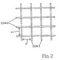
- first electrically conductive layer M 1is then patterned by any suitable technique, such as masking followed by etching as understood by persons skilled in the art, to form a set of first transmission or communication lines COM 1 . While the cross-section of only one communication line COM 1 is illustrated in FIG. 1B , it will be appreciated by persons skilled in the art that first electrically conductive layer M 1 can preferably be patterned to form a plurality of spaced-apart communication lines COM 1 on first dielectric isolation layer D 1 to provide multiple routes for electrical signals, as exemplified in the cross-bar configuration illustrated in FIG. 2 .
- a second dielectric isolation layer D 2is formed on the pattern of first communication lines COM 1 and on the exposed regions of first dielectric isolation layer D 1 .
- second dielectric isolation layer D 2is preferably composed of a suitable low-k dielectric material such as SiO 2 .
- a thermally conductive layer HSis then formed on second dielectric isolation layer D 2 to serve as a heat spreader.
- the out-of-plane thickness of thermally conductive layer HScan range from approximately 0.1 to approximately 1 microns.
- Thermally conductive layer HScan include any material that is thermally conductive such as, for example, gold (Au), copper, aluminum (Al), and diamond.
- thermally conductive layer HSIn the case of gold, a physical deposition technique such as sputtering can be employed to form thermally conductive layer HS, although alternative techniques such as electroplating could be employed.
- a third dielectric isolation layer D 3is formed on thermally conductive layer HS.
- third dielectric isolation layer D 3is preferably composed of a suitable low-k dielectric material such as SiO 2 .
- a second electrically conductive layer M 2is formed on third dielectric isolation layer D 3 .
- second electrically conductive layer M 2is preferably composed of a metal such as copper.
- Second electrically conductive layer M 2is then patterned by any suitable technique to form a second set of communication lines COM 2 , which in typical embodiments are arranged generally orthogonally relative to the first set of communication lines COM 1 formed from first electrically conductive layer Ml. While a section of only one communication line COM 2 of second electrically conductive layer M 2 is illustrated in FIG. 1F , it will be appreciated by persons skilled in the art that second electrically conductive layer M 2 is preferably patterned to form a plurality of spaced-apart communication lines COM 2 on third dielectric isolation layer D 3 , as shown in FIG. 2 .
- fourth dielectric isolation layer D 4is preferably composed of a suitable low-k dielectric material such as SiO 2 .
- FIGS. 1A-1Gshow the conformal deposition of dielectric isolation layers D 2 -D 4 , thermally conductive layer HS, and second electrically conductive layer M 2 around the shape of the first communication lines COM 1 formed from first electrically conductive layer M 1 .
- some or all of these layerscould be planarized.
- second dielectric isolation layer D 2could be deposited and planarized to a specific thickness above first communication lines COM 1 .
- Second dielectric isolation layer D 2could be planarized by a process such as chemical-mechanical polishing (CMP).
- CMPchemical-mechanical polishing
- Third dielectric isolation layer D 3would then be deposited on thermally conductive layer HS.
- Third dielectric layer D 3 and thermally conductive layer HSare largely planar because they are deposited on a planar surface.
- Second electrically conductive layer M 2would be deposited on third dielectric isolation layer D 3 , which is a planar surface.
- Fourth dielectric isolation layer D 4is deposited on third dielectric isolation layer D 3 and second electrically conductive layer M 2 and planarized to a specific thickness above second electrically conductive layer M 2 .
- Fourth dielectric isolation layer D 4could be planarized by methods such as chemical-mechanical polishing (CMP).
- CMPchemical-mechanical polishing
- the benefits of the heat spreader HS layerare realized for a planar process or a conformal process, if the widths of communication lines COM 1 and second communication lines COM 2 lines are large relative to their thickness. In either case, most of the heat flow would be between the first electrically conductive layer M 1 and second electrically conductive layer M 2 rather than laterally between first communication lines COM 1 or second communication lines COM 2 .
- the goal of the heat spreaderis to accomplish driving the heat flow laterally and reducing the localized temperature, especially by driving heat energy away from likely hot spots such as regions where communication lines COM 1 and COM 2 cross each other. If the width and thickness of the first electrically conductive layer M 1 and second electrically conductive layer M 2 lines are of comparable magnitude, the conformal process might provide greater heat spreading (local temperature reduction) than the planarized case.
- FIG. 1Gis a cross-sectional depiction of a portion of the resulting interconnect device 10 .
- a high-density array or grid of several rows and columns of communication lines COM 1 and COM 2is formed from first and second electrically conductive layers M 1 and M 2 , as exemplified in the cross-bar configuration illustrated in FIG. 2 .
- First communication lines COM 1are disposed generally along a first plane and second communication lines COM 2 are disposed generally along a second plane that is spaced from the first plane.
- the spacing between first communication lines COM 1 and second communication lines COM 2can range from approximately 3 to approximately 8 microns.
- the spacing between each adjacent, co-planar pair of first communication lines COM 1 , and between each adjacent, co-planar pair of second communication lines COM 2 ,is indicated by a distance d in FIG. 2 .
- Distance dcan range from approximately 25 to approximately 250 microns, and preferably is approximately 125 microns. In one embodiment, distance d between all adjacent, coplanar pairs of communication lines COM 1 and COM 2 is uniform. By evenly spacing communication lines COM 1 and COM 2 in this manner, the distribution of heat energy through interconnect device 10 is rendered more uniform which, for large interconnect densities, can assist in reducing the maximum operating temperature in addition to the integration of thermally conductive layer HS.
- the width of each communication line COM 1 and COM 2 across the layer on which it is formedcan range from approximately 10 to approximately 100 microns, and preferably is approximately 100 microns.
- the thickness of each communication line COM 1 and COM 2 on its corresponding layercan range from approximately 1 to approximately 5 microns, and preferably is approximately 3 microns.
- the thickness of first dielectric isolation layer D 1is typically 0.5 to 1 micron.
- the thickness of second dielectric isolation layer D 2is typically 1 to 5 microns, and preferably is approximately 1.5 microns.
- the thickness of third dielectric isolation layer D 3is typically 1 to 5 microns, and preferably is approximately 1.5 microns.
- the thickness of fourth dielectric isolation layer D 4is typically 1 to 5 microns, and preferably is approximately 3 microns.
- one design goal enabled by the inventionis to minimize the resistance of the communication lines COM 1 and COM 2 and minimize the heating that results from a self-heating process.
- the dimensions of the dielectric and conductive layersare optimized with regard to resistance, heating, temperature, and capacitive coupling.
- the volume fraction of the electrically conductive layers to the dielectric layersis optimized to minimize the stress and curvature that are developed in substrate S with regard to residual stress fields within the layers, with regard to differences in thermal coefficients of expansion, or with regard to temperature gradients through the layers and substrate S.
- thermally conductive layer HS constituting the heat spreaderis sandwiched between first and second communication lines COM 1 and COM 2 formed from first and second electrically conductive layers M 1 and M 2 , respectively, as a buried, integral component of interconnect device 10 .
- Second and third dielectric isolation layers D 2 and D 3electrically isolate thermally conductive layer HS from first and second electrically conductive layers M 1 and M 2 , respectively.
- First dielectric isolation layer D 1electrically isolates the as-built conductive/non-conductive heterostructure of interconnect device 10 from its substrate S.
- Fourth dielectric isolation layer D 4electrically isolates second communication lines COM 2 of second electrically conductive layer M 2 from any circuitry or devices fabricated on interconnect device 10 .
- thermally conductive layer HSis preferably composed of a metal such as gold, and thus preferably is also electrically conductive. Accordingly, it will be noted that any two of the three metal layers illustrated in FIG. 1G could serve as first and second electrically conductive layers M 1 and M 2 for forming first and second communication lines COM 1 and COM 2 , with the remaining third metal layer serving as thermally conductive layer HS and thus as the heat spreader. However, in the embodiment illustrated in FIG. 1G in which thermally conductive layer HS is sandwiched between first and second communication lines COM 1 and COM 2 , thermally conductive layer HS could additionally function as a capacitive shield.
- thermally conductive layer HSBy providing proper grounding to thermally conductive layer HS, out-of-plane capacitive coupling between first and second communication lines COM 1 and COM 2 could be reduced in at least some embodiments. Additionally, a thermally conductive layer HS added between substrate S and the communication lines COM 1 and COM 2 will block the electromagnetic coupling to substrate S. The electrostatic shielding is applicable for capacitive coupling and RF pads for application at “low frequencies”. In this example of capacitive coupling, thermally conductive layer HS can be largely unpatterned with the exception of regions where connections will be established between first and second communication lines COM 1 and COM 2 . Additionally, thermally conductive layer HS can be patterned to reduce the total amount of metalization used while maintaining the thermal advantage.
- thermally conductive layer HSwill need to be patterned for it to provide shielding when inductors are part of substrate S.
- the shieldneeds to be patterned to limit the effect of eddy currents, which produce opposing magnetic fields resulting in reduced energy storage and reduced Q (quality factor).
- the design of the shield for inductor applicationsis known to those skilled in the art and is not described further herein.
- a micro-scale systemgenerally designated 100 , includes the heterostructure of interconnect device 10 as integrated with any other micro-scale device, circuitry, or instrument fabricated typically on the heterostructure at device region 105 A, and/or at device regions 105 B, 105 C, and 105 D.
- device regions 105 A, 105 B, 105 C, and/or 105 Dcould represent microelectronic devices or integrated circuits having active and/or passive circuit elements such as transistors, resistors, capacitors, MOS or related circuit components, contacts, electrodes, and electrical leads; opto-electronic and photonic devices such as windows, lenses, light-emitting diodes (LEDs), laser diodes (LDs), photodiode arrays, mirrors, filters, flat-panel displays, and waveguides; micromechanical devices such as deflectable cantilevers and membranes, and encapsulating, structural, or packaging components; MEMS devices such as microrelays, micromotors, gyroscopes, accelerometers, and thermally-induced components and transducers in general; MOEMS devices such as movable optical shutters, attenuators, electromagnetic radiation detectors, and switches; chip-based biosensors and chemosensors; and microfluidic devices such as labs-on-a-chip (L
- the unit cellis representative of a DC switch array having an interconnect scheme as illustrated in FIG. 1 G.
- the dielectric material considered for the isolation layerswas silica
- the metal considered for the electrically conductive layerswas copper
- the metal considered for the thermally conductive heat spreading layerwas gold.
- the width of the unit cellis 40 microns and the thickness (t i ) is varied along the horizontal axis of the data plot. As further indicated in FIG.
- maximum operating temperatureis plotted as a function of unit cell thickness for three separate cases: a heat spreader thickness of zero (i.e., no heat spreader), 0.1 micron, and 1 micron. It can be observed from FIG. 4 that the presence of a 1-micron thick heat spreader significantly reduces maximum temperature reached in the unit cell at progressively greater unit cell thicknesses. Moreover, FIG. 4 shows that the gains observed due to the incorporation of the heat spreader are more significant moving down to thinner transmission lines. Also, the reduction obtained would be significant at even higher current magnitudes due the current-squared dependence of the Joule Heating effect.
Landscapes
- Engineering & Computer Science (AREA)
- Microelectronics & Electronic Packaging (AREA)
- Computer Hardware Design (AREA)
- Chemical & Material Sciences (AREA)
- Power Engineering (AREA)
- General Physics & Mathematics (AREA)
- Physics & Mathematics (AREA)
- Manufacturing & Machinery (AREA)
- Condensed Matter Physics & Semiconductors (AREA)
- Analytical Chemistry (AREA)
- Ceramic Engineering (AREA)
- Materials Engineering (AREA)
- Micromachines (AREA)
- Gyroscopes (AREA)
- Internal Circuitry In Semiconductor Integrated Circuit Devices (AREA)
- Pressure Sensors (AREA)
- Mechanical Light Control Or Optical Switches (AREA)
- Measurement And Recording Of Electrical Phenomena And Electrical Characteristics Of The Living Body (AREA)
- Multi-Conductor Connections (AREA)
- Buffer Packaging (AREA)
- Wire Bonding (AREA)
- Lead Frames For Integrated Circuits (AREA)
- Coupling Device And Connection With Printed Circuit (AREA)
- Design And Manufacture Of Integrated Circuits (AREA)
- Air Bags (AREA)
- Treatment Of Fiber Materials (AREA)
- Switches Operated By Changes In Physical Conditions (AREA)
- Thermally Actuated Switches (AREA)
- Bending Of Plates, Rods, And Pipes (AREA)
- Apparatuses And Processes For Manufacturing Resistors (AREA)
- Cooling Or The Like Of Semiconductors Or Solid State Devices (AREA)
Abstract
Description
Claims (29)
Priority Applications (2)
| Application Number | Priority Date | Filing Date | Title |
|---|---|---|---|
| US10/291,146US6847114B2 (en) | 2001-11-09 | 2002-11-08 | Micro-scale interconnect device with internal heat spreader and method for fabricating same |
| US10/831,012US20040197960A1 (en) | 2001-11-09 | 2004-04-22 | Micro-scale interconnect device with internal heat spreader and method for fabricating same |
Applications Claiming Priority (7)
| Application Number | Priority Date | Filing Date | Title |
|---|---|---|---|
| US33805501P | 2001-11-09 | 2001-11-09 | |
| US33752801P | 2001-11-09 | 2001-11-09 | |
| US33752901P | 2001-11-09 | 2001-11-09 | |
| US33752701P | 2001-11-09 | 2001-11-09 | |
| US33807201P | 2001-11-09 | 2001-11-09 | |
| US33806901P | 2001-11-09 | 2001-11-09 | |
| US10/291,146US6847114B2 (en) | 2001-11-09 | 2002-11-08 | Micro-scale interconnect device with internal heat spreader and method for fabricating same |
Related Child Applications (1)
| Application Number | Title | Priority Date | Filing Date |
|---|---|---|---|
| US10/831,012DivisionUS20040197960A1 (en) | 2001-11-09 | 2004-04-22 | Micro-scale interconnect device with internal heat spreader and method for fabricating same |
Publications (2)
| Publication Number | Publication Date |
|---|---|
| US20030116851A1 US20030116851A1 (en) | 2003-06-26 |
| US6847114B2true US6847114B2 (en) | 2005-01-25 |
Family
ID=27559772
Family Applications (9)
| Application Number | Title | Priority Date | Filing Date |
|---|---|---|---|
| US10/291,107Expired - LifetimeUS6876482B2 (en) | 2001-11-09 | 2002-11-08 | MEMS device having contact and standoff bumps and related methods |
| US10/290,779Expired - LifetimeUS6876047B2 (en) | 2001-11-09 | 2002-11-08 | MEMS device having a trilayered beam and related methods |
| US10/290,920Expired - LifetimeUS6746891B2 (en) | 2001-11-09 | 2002-11-08 | Trilayered beam MEMS device and related methods |
| US10/290,807Expired - Fee RelatedUS6882264B2 (en) | 2001-11-09 | 2002-11-08 | Electrothermal self-latching MEMS switch and method |
| US10/291,125Expired - Fee RelatedUS8264054B2 (en) | 2001-11-09 | 2002-11-08 | MEMS device having electrothermal actuation and release and method for fabricating |
| US10/291,146Expired - LifetimeUS6847114B2 (en) | 2001-11-09 | 2002-11-08 | Micro-scale interconnect device with internal heat spreader and method for fabricating same |
| US10/817,270Expired - LifetimeUS6917086B2 (en) | 2001-11-09 | 2004-04-02 | Trilayered beam MEMS device and related methods |
| US10/831,012AbandonedUS20040197960A1 (en) | 2001-11-09 | 2004-04-22 | Micro-scale interconnect device with internal heat spreader and method for fabricating same |
| US11/492,671Expired - LifetimeUS8420427B2 (en) | 2001-11-09 | 2006-07-25 | Methods for implementation of a switching function in a microscale device and for fabrication of a microscale switch |
Family Applications Before (5)
| Application Number | Title | Priority Date | Filing Date |
|---|---|---|---|
| US10/291,107Expired - LifetimeUS6876482B2 (en) | 2001-11-09 | 2002-11-08 | MEMS device having contact and standoff bumps and related methods |
| US10/290,779Expired - LifetimeUS6876047B2 (en) | 2001-11-09 | 2002-11-08 | MEMS device having a trilayered beam and related methods |
| US10/290,920Expired - LifetimeUS6746891B2 (en) | 2001-11-09 | 2002-11-08 | Trilayered beam MEMS device and related methods |
| US10/290,807Expired - Fee RelatedUS6882264B2 (en) | 2001-11-09 | 2002-11-08 | Electrothermal self-latching MEMS switch and method |
| US10/291,125Expired - Fee RelatedUS8264054B2 (en) | 2001-11-09 | 2002-11-08 | MEMS device having electrothermal actuation and release and method for fabricating |
Family Applications After (3)
| Application Number | Title | Priority Date | Filing Date |
|---|---|---|---|
| US10/817,270Expired - LifetimeUS6917086B2 (en) | 2001-11-09 | 2004-04-02 | Trilayered beam MEMS device and related methods |
| US10/831,012AbandonedUS20040197960A1 (en) | 2001-11-09 | 2004-04-22 | Micro-scale interconnect device with internal heat spreader and method for fabricating same |
| US11/492,671Expired - LifetimeUS8420427B2 (en) | 2001-11-09 | 2006-07-25 | Methods for implementation of a switching function in a microscale device and for fabrication of a microscale switch |
Country Status (7)
| Country | Link |
|---|---|
| US (9) | US6876482B2 (en) |
| EP (9) | EP1454333B1 (en) |
| CN (3) | CN1292447C (en) |
| AT (8) | ATE352854T1 (en) |
| AU (3) | AU2002359370A1 (en) |
| DE (7) | DE60229675D1 (en) |
| WO (6) | WO2003043038A2 (en) |
Cited By (11)
| Publication number | Priority date | Publication date | Assignee | Title |
|---|---|---|---|---|
| US20030220012A1 (en)* | 2002-05-24 | 2003-11-27 | Stewart Robert E. | Compliant component for supporting electrical interface component |
| US20050194179A1 (en)* | 2004-03-04 | 2005-09-08 | Au Optronics Corporation | Method for reducing voltage drop across metal lines of electroluminescence display devices |
| US20070063788A1 (en)* | 2005-09-22 | 2007-03-22 | Samsung Electronics Co., Ltd. | System and method for a digitally tunable impedance matching network |
| US20070194859A1 (en)* | 2006-02-17 | 2007-08-23 | Samsung Electronics Co., Ltd. | System and method for a tunable impedance matching network |
| US20070216274A1 (en)* | 2006-03-17 | 2007-09-20 | 3M Innovative Properties Company | Illumination assembly with enhanced thermal conductivity |
| US20080094149A1 (en)* | 2005-09-22 | 2008-04-24 | Sungsung Electronics Co., Ltd. | Power amplifier matching circuit and method using tunable mems devices |
| US7400015B1 (en)* | 2007-01-15 | 2008-07-15 | International Business Machines Corporation | Semiconductor structure with field shield and method of forming the structure |
| US20110156245A1 (en)* | 2009-12-31 | 2011-06-30 | Taiwan Semiconductor Manufacturing Company, Ltd. | Method and Apparatus for Cooling an Integrated Circuit |
| US8458888B2 (en) | 2010-06-25 | 2013-06-11 | International Business Machines Corporation | Method of manufacturing a micro-electro-mechanical system (MEMS) |
| US8637775B2 (en)* | 2010-04-07 | 2014-01-28 | Samsung Electro-Mechanics Co., Ltd. | Printed circuit board and method of manufacturing the same |
| WO2023059519A3 (en)* | 2021-10-04 | 2023-07-20 | Formfactor, Inc. | Thermal management techniques for high power integrated circuits operating in dry cryogenic environments |
Families Citing this family (316)
| Publication number | Priority date | Publication date | Assignee | Title |
|---|---|---|---|---|
| US6853067B1 (en) | 1999-10-12 | 2005-02-08 | Microassembly Technologies, Inc. | Microelectromechanical systems using thermocompression bonding |
| US20020096421A1 (en)* | 2000-11-29 | 2002-07-25 | Cohn Michael B. | MEMS device with integral packaging |
| JP3651671B2 (en)* | 2001-08-30 | 2005-05-25 | 株式会社東芝 | Micromechanical switch and manufacturing method thereof |
| US7132736B2 (en)* | 2001-10-31 | 2006-11-07 | Georgia Tech Research Corporation | Devices having compliant wafer-level packages with pillars and methods of fabrication |
| DE60229675D1 (en)* | 2001-11-09 | 2008-12-11 | Wispry Inc | Three-layer beam MEMS device and related methods |
| US7521366B2 (en)* | 2001-12-12 | 2009-04-21 | Lg Display Co., Ltd. | Manufacturing method of electro line for liquid crystal display device |
| US7045459B2 (en)* | 2002-02-19 | 2006-05-16 | Northrop Grumman Corporation | Thin film encapsulation of MEMS devices |
| US7763947B2 (en)* | 2002-04-23 | 2010-07-27 | Sharp Laboratories Of America, Inc. | Piezo-diode cantilever MEMS |
| US7135777B2 (en)* | 2002-05-03 | 2006-11-14 | Georgia Tech Research Corporation | Devices having compliant wafer-level input/output interconnections and packages using pillars and methods of fabrication thereof |
| US6777258B1 (en)* | 2002-06-28 | 2004-08-17 | Silicon Light Machines, Inc. | Conductive etch stop for etching a sacrificial layer |
| US7064637B2 (en)* | 2002-07-18 | 2006-06-20 | Wispry, Inc. | Recessed electrode for electrostatically actuated structures |
| US7551048B2 (en)* | 2002-08-08 | 2009-06-23 | Fujitsu Component Limited | Micro-relay and method of fabricating the same |
| EP1394554B1 (en)* | 2002-08-30 | 2011-11-02 | STMicroelectronics Srl | Process for the fabrication of a threshold acceleration sensor |
| US20040121505A1 (en)* | 2002-09-30 | 2004-06-24 | Magfusion, Inc. | Method for fabricating a gold contact on a microswitch |
| US7053736B2 (en)* | 2002-09-30 | 2006-05-30 | Teravicta Technologies, Inc. | Microelectromechanical device having an active opening switch |
| US7317232B2 (en)* | 2002-10-22 | 2008-01-08 | Cabot Microelectronics Corporation | MEM switching device |
| US6835589B2 (en)* | 2002-11-14 | 2004-12-28 | International Business Machines Corporation | Three-dimensional integrated CMOS-MEMS device and process for making the same |
| US6800503B2 (en)* | 2002-11-20 | 2004-10-05 | International Business Machines Corporation | MEMS encapsulated structure and method of making same |
| US7498911B2 (en)* | 2003-02-26 | 2009-03-03 | Memtronics Corporation | Membrane switch components and designs |
| EP1609206B1 (en) | 2003-03-04 | 2010-07-28 | Rohm and Haas Electronic Materials, L.L.C. | Coaxial waveguide microstructures and methods of formation thereof |
| US6720267B1 (en)* | 2003-03-19 | 2004-04-13 | United Microelectronics Corp. | Method for forming a cantilever beam model micro-electromechanical system |
| NL1023275C2 (en)* | 2003-04-25 | 2004-10-27 | Cavendish Kinetics Ltd | Method for manufacturing a micro-mechanical element. |
| CA2429909A1 (en)* | 2003-05-27 | 2004-11-27 | Cognos Incorporated | Transformation of tabular and cross-tabulated queries based upon e/r schema into multi-dimensional expression queries |
| DE10325564B4 (en)* | 2003-06-05 | 2008-12-18 | Infineon Technologies Ag | Smart card module |
| US7061022B1 (en)* | 2003-08-26 | 2006-06-13 | United States Of America As Represented By The Secretary Of The Army | Lateral heat spreading layers for epi-side up ridge waveguide semiconductor lasers |
| JP4823478B2 (en)* | 2003-09-19 | 2011-11-24 | 株式会社半導体エネルギー研究所 | Method for manufacturing light emitting device |
| US7520790B2 (en)* | 2003-09-19 | 2009-04-21 | Semiconductor Energy Laboratory Co., Ltd. | Display device and manufacturing method of display device |
| US7388459B2 (en)* | 2003-10-28 | 2008-06-17 | Medtronic, Inc. | MEMs switching circuit and method for an implantable medical device |
| US7283024B2 (en)* | 2003-12-18 | 2007-10-16 | Intel Corporation | MEMS switch stopper bumps with adjustable height |
| GB0330010D0 (en)* | 2003-12-24 | 2004-01-28 | Cavendish Kinetics Ltd | Method for containing a device and a corresponding device |
| US7142087B2 (en)* | 2004-01-27 | 2006-11-28 | Lucent Technologies Inc. | Micromechanical latching switch |
| US7101724B2 (en)* | 2004-02-20 | 2006-09-05 | Wireless Mems, Inc. | Method of fabricating semiconductor devices employing at least one modulation doped quantum well structure and one or more etch stop layers for accurate contact formation |
| US20050244099A1 (en)* | 2004-03-24 | 2005-11-03 | Pasch Nicholas F | Cantilevered micro-electromechanical switch array |
| US7362199B2 (en)* | 2004-03-31 | 2008-04-22 | Intel Corporation | Collapsible contact switch |
| FR2868591B1 (en)* | 2004-04-06 | 2006-06-09 | Commissariat Energie Atomique | MICROCOMMUTER WITH LOW ACTUATION VOLTAGE AND LOW CONSUMPTION |
| US7476327B2 (en)* | 2004-05-04 | 2009-01-13 | Idc, Llc | Method of manufacture for microelectromechanical devices |
| DE102004026654B4 (en)* | 2004-06-01 | 2009-07-09 | Fraunhofer-Gesellschaft zur Förderung der angewandten Forschung e.V. | Micromechanical RF switching element and method of manufacture |
| US7749792B2 (en)* | 2004-06-02 | 2010-07-06 | Carnegie Mellon University | Self-assembling MEMS devices having thermal actuation |
| US20060055499A1 (en)* | 2004-09-16 | 2006-03-16 | Bolle Cristian A | Fuse arrangement |
| US7564612B2 (en) | 2004-09-27 | 2009-07-21 | Idc, Llc | Photonic MEMS and structures |
| US7583429B2 (en) | 2004-09-27 | 2009-09-01 | Idc, Llc | Ornamental display device |
| US7420725B2 (en) | 2004-09-27 | 2008-09-02 | Idc, Llc | Device having a conductive light absorbing mask and method for fabricating same |
| US7372613B2 (en) | 2004-09-27 | 2008-05-13 | Idc, Llc | Method and device for multistate interferometric light modulation |
| US7289259B2 (en) | 2004-09-27 | 2007-10-30 | Idc, Llc | Conductive bus structure for interferometric modulator array |
| US7417783B2 (en)* | 2004-09-27 | 2008-08-26 | Idc, Llc | Mirror and mirror layer for optical modulator and method |
| US7527995B2 (en) | 2004-09-27 | 2009-05-05 | Qualcomm Mems Technologies, Inc. | Method of making prestructure for MEMS systems |
| US8008736B2 (en) | 2004-09-27 | 2011-08-30 | Qualcomm Mems Technologies, Inc. | Analog interferometric modulator device |
| US20060065622A1 (en)* | 2004-09-27 | 2006-03-30 | Floyd Philip D | Method and system for xenon fluoride etching with enhanced efficiency |
| US7630119B2 (en) | 2004-09-27 | 2009-12-08 | Qualcomm Mems Technologies, Inc. | Apparatus and method for reducing slippage between structures in an interferometric modulator |
| US7304784B2 (en)* | 2004-09-27 | 2007-12-04 | Idc, Llc | Reflective display device having viewable display on both sides |
| US7936497B2 (en) | 2004-09-27 | 2011-05-03 | Qualcomm Mems Technologies, Inc. | MEMS device having deformable membrane characterized by mechanical persistence |
| US7944599B2 (en) | 2004-09-27 | 2011-05-17 | Qualcomm Mems Technologies, Inc. | Electromechanical device with optical function separated from mechanical and electrical function |
| US7369296B2 (en) | 2004-09-27 | 2008-05-06 | Idc, Llc | Device and method for modifying actuation voltage thresholds of a deformable membrane in an interferometric modulator |
| US7193492B2 (en)* | 2004-09-29 | 2007-03-20 | Lucent Technologies Inc. | Monolithic MEMS device having a balanced cantilever plate |
| US7239064B1 (en)* | 2004-10-15 | 2007-07-03 | Morgan Research Corporation | Resettable latching MEMS temperature sensor apparatus and method |
| KR100619110B1 (en) | 2004-10-21 | 2006-09-04 | 한국전자통신연구원 | Microelectromechanical switch and method of manufacturing the same |
| US7230513B2 (en)* | 2004-11-20 | 2007-06-12 | Wireless Mems, Inc. | Planarized structure for a reliable metal-to-metal contact micro-relay MEMS switch |
| TWI252838B (en)* | 2004-12-02 | 2006-04-11 | Delta Electronics Inc | Micro-switch |
| US7385800B2 (en)* | 2004-12-09 | 2008-06-10 | Wispry, Inc. | Micro-electro-mechanical system (MEMS) capacitors, inductors, and related systems and methods |
| US7391090B2 (en)* | 2004-12-17 | 2008-06-24 | Hewlett-Packard Development Company, L.P. | Systems and methods for electrically coupling wires and conductors |
| KR100661176B1 (en)* | 2004-12-17 | 2006-12-26 | 삼성전자주식회사 | MEMS switch and its manufacturing method |
| US7521784B2 (en)* | 2004-12-17 | 2009-04-21 | Hewlett-Packard Development Company, L.P. | System for coupling wire to semiconductor region |
| US7597819B1 (en)* | 2004-12-20 | 2009-10-06 | Sandia Corporation | Redox buffered hydrofluoric acid etchant for the reduction of galvanic attack during release etching of MEMS devices having noble material films |
| TWI287634B (en)* | 2004-12-31 | 2007-10-01 | Wen-Chang Dung | Micro-electromechanical probe circuit film, method for making the same and applications thereof |
| US7601554B1 (en) | 2005-01-31 | 2009-10-13 | The United States Of America As Represented By The Secretary Of The Air Force | Shaped MEMS contact |
| US7235750B1 (en) | 2005-01-31 | 2007-06-26 | United States Of America As Represented By The Secretary Of The Air Force | Radio frequency MEMS switch contact metal selection |
| US7655996B1 (en)* | 2005-02-03 | 2010-02-02 | The United States Of America As Represented By The Secretary Of The Army | MEMS structure support and release mechanism |
| US7404167B2 (en) | 2005-02-23 | 2008-07-22 | Taiwan Semiconductor Manufacturing Company, Ltd. | Method for improving design window |
| JP4707424B2 (en)* | 2005-03-18 | 2011-06-22 | 株式会社東芝 | Variable capacitance element, variable capacitance device, and mobile phone using variable capacitance device |
| KR20080019577A (en)* | 2005-03-18 | 2008-03-04 | 심플러 네트웍스, 인코포레이티드 | MEMS actuators and MEMS switches |
| JP4498181B2 (en)* | 2005-03-22 | 2010-07-07 | 東京エレクトロン株式会社 | Switch array |
| KR20070117695A (en)* | 2005-03-31 | 2007-12-12 | 몰렉스 인코포레이티드 | High Density Rigid Connectors with Castelation |
| DE102005016243B3 (en) | 2005-04-08 | 2006-09-28 | Austriamicrosystems Ag | Micromechanical component e.g. micro electro mechanical system structure, for use as e.g. micro sensor, has one metal layer of multi-layer structure extending at side over pile and electrically conductive membrane integrated in structure |
| FR2885735B1 (en)* | 2005-05-10 | 2007-08-03 | St Microelectronics Sa | INTEGRATED CIRCUIT WAVE GUIDE |
| US7692521B1 (en)* | 2005-05-12 | 2010-04-06 | Microassembly Technologies, Inc. | High force MEMS device |
| US7884989B2 (en)* | 2005-05-27 | 2011-02-08 | Qualcomm Mems Technologies, Inc. | White interferometric modulators and methods for forming the same |
| US7321275B2 (en)* | 2005-06-23 | 2008-01-22 | Intel Corporation | Ultra-low voltage capable zipper switch |
| KR101375337B1 (en) | 2005-07-22 | 2014-03-18 | 퀄컴 엠이엠에스 테크놀로지스, 인크. | Electomechanical devices having support structures and methods of fabricating the same |
| JP4489651B2 (en)* | 2005-07-22 | 2010-06-23 | 株式会社日立製作所 | Semiconductor device and manufacturing method thereof |
| EP2495212A3 (en) | 2005-07-22 | 2012-10-31 | QUALCOMM MEMS Technologies, Inc. | Mems devices having support structures and methods of fabricating the same |
| US7612635B2 (en)* | 2005-08-03 | 2009-11-03 | Kolo Technologies, Inc. | MEMS acoustic filter and fabrication of the same |
| US20070040637A1 (en)* | 2005-08-19 | 2007-02-22 | Yee Ian Y K | Microelectromechanical switches having mechanically active components which are electrically isolated from components of the switch used for the transmission of signals |
| US7528691B2 (en)* | 2005-08-26 | 2009-05-05 | Innovative Micro Technology | Dual substrate electrostatic MEMS switch with hermetic seal and method of manufacture |
| US7569926B2 (en)* | 2005-08-26 | 2009-08-04 | Innovative Micro Technology | Wafer level hermetic bond using metal alloy with raised feature |
| US20070048887A1 (en)* | 2005-08-26 | 2007-03-01 | Innovative Micro Technology | Wafer level hermetic bond using metal alloy |
| US7233048B2 (en)* | 2005-08-26 | 2007-06-19 | Innovative Micro Technology | MEMS device trench plating process and apparatus for through hole vias |
| US8736081B2 (en) | 2005-08-26 | 2014-05-27 | Innovative Micro Technology | Wafer level hermetic bond using metal alloy with keeper layer |
| US7582969B2 (en)* | 2005-08-26 | 2009-09-01 | Innovative Micro Technology | Hermetic interconnect structure and method of manufacture |
| US7960208B2 (en)* | 2005-08-26 | 2011-06-14 | Innovative Micro Technology | Wafer level hermetic bond using metal alloy with raised feature |
| US20070090474A1 (en)* | 2005-09-08 | 2007-04-26 | Li Gary G | MEMS device and method of fabrication |
| EP1928780A2 (en)* | 2005-09-30 | 2008-06-11 | Qualcomm Mems Technologies, Inc. | Mems device and interconnects for same |
| KR100827314B1 (en)* | 2005-10-10 | 2008-05-06 | 삼성전기주식회사 | Method of manufacturing MEMS element and optical modulator having flat surface by heat treatment |
| US8043950B2 (en) | 2005-10-26 | 2011-10-25 | Semiconductor Energy Laboratory Co., Ltd. | Semiconductor device and manufacturing method thereof |
| US7630114B2 (en)* | 2005-10-28 | 2009-12-08 | Idc, Llc | Diffusion barrier layer for MEMS devices |
| US20070096860A1 (en)* | 2005-11-02 | 2007-05-03 | Innovative Micro Technology | Compact MEMS thermal device and method of manufacture |
| KR100744543B1 (en)* | 2005-12-08 | 2007-08-01 | 한국전자통신연구원 | Micro-electro mechanical systems switch and method of fabricating the same switch |
| CA2632875A1 (en)* | 2005-12-12 | 2007-06-21 | Telezygology Inc. | Developments in beam type fasteners |
| WO2007072407A2 (en)* | 2005-12-22 | 2007-06-28 | Nxp B.V. | Arrangement of mems devices having series coupled capacitors |
| US7602261B2 (en)* | 2005-12-22 | 2009-10-13 | Intel Corporation | Micro-electromechanical system (MEMS) switch |
| US7525151B2 (en)* | 2006-01-05 | 2009-04-28 | International Rectifier Corporation | Vertical DMOS device in integrated circuit |
| FR2895986B1 (en)* | 2006-01-06 | 2008-09-05 | Centre Nat Rech Scient | PREPARATION OF MULTILAYER MICROCOMPONENTS BY THE METHOD OF THE SACRIFICIAL THICK LAYER |
| US20070196048A1 (en)* | 2006-01-12 | 2007-08-23 | Almantas Galvanauskas | Optical waveform shaping |
| US7916980B2 (en) | 2006-01-13 | 2011-03-29 | Qualcomm Mems Technologies, Inc. | Interconnect structure for MEMS device |
| US7382515B2 (en) | 2006-01-18 | 2008-06-03 | Qualcomm Mems Technologies, Inc. | Silicon-rich silicon nitrides as etch stops in MEMS manufacture |
| US7678601B2 (en)* | 2006-01-20 | 2010-03-16 | Texas Instruments Incorporated | Method of forming an acceleration sensor |
| US20070170528A1 (en)* | 2006-01-20 | 2007-07-26 | Aaron Partridge | Wafer encapsulated microelectromechanical structure and method of manufacturing same |
| US7463113B2 (en)* | 2006-02-28 | 2008-12-09 | Motorla, Inc. | Apparatus and methods relating to electrically conductive path interfaces disposed within capacitor plate openings |
| US7480432B2 (en)* | 2006-02-28 | 2009-01-20 | Corning Incorporated | Glass-based micropositioning systems and methods |
| CN101438366B (en)* | 2006-03-08 | 2011-10-26 | 维斯普瑞公司 | Microelectromechanical systems (MEMS) variable capacitors, actuation components, and related methods |
| US7711239B2 (en) | 2006-04-19 | 2010-05-04 | Qualcomm Mems Technologies, Inc. | Microelectromechanical device and method utilizing nanoparticles |
| US7417784B2 (en) | 2006-04-19 | 2008-08-26 | Qualcomm Mems Technologies, Inc. | Microelectromechanical device and method utilizing a porous surface |
| US7623287B2 (en) | 2006-04-19 | 2009-11-24 | Qualcomm Mems Technologies, Inc. | Non-planar surface structures and process for microelectromechanical systems |
| US7554421B2 (en)* | 2006-05-16 | 2009-06-30 | Intel Corporation | Micro-electromechanical system (MEMS) trampoline switch/varactor |
| GB0610392D0 (en) | 2006-05-25 | 2006-07-05 | Univ Durham | Electro-mechanical actuator and apparatus incorporating such device |
| US7649671B2 (en) | 2006-06-01 | 2010-01-19 | Qualcomm Mems Technologies, Inc. | Analog interferometric modulator device with electrostatic actuation and release |
| US7405863B2 (en) | 2006-06-01 | 2008-07-29 | Qualcomm Mems Technologies, Inc. | Patterning of mechanical layer in MEMS to reduce stresses at supports |
| US7605675B2 (en)* | 2006-06-20 | 2009-10-20 | Intel Corporation | Electromechanical switch with partially rigidified electrode |
| US7835061B2 (en) | 2006-06-28 | 2010-11-16 | Qualcomm Mems Technologies, Inc. | Support structures for free-standing electromechanical devices |
| US7527998B2 (en) | 2006-06-30 | 2009-05-05 | Qualcomm Mems Technologies, Inc. | Method of manufacturing MEMS devices providing air gap control |
| US7911010B2 (en)* | 2006-07-17 | 2011-03-22 | Kwj Engineering, Inc. | Apparatus and method for microfabricated multi-dimensional sensors and sensing systems |
| JP4234737B2 (en)* | 2006-07-24 | 2009-03-04 | 株式会社東芝 | MEMS switch |
| JP4265630B2 (en)* | 2006-08-04 | 2009-05-20 | セイコーエプソン株式会社 | MEMS switch, voltage divider circuit, gain adjustment circuit, attenuator, and method of manufacturing MEMS switch |
| JP2010500711A (en)* | 2006-08-09 | 2010-01-07 | コーニンクレッカ フィリップス エレクトロニクス エヌ ヴィ | Self-locking micro electromechanical element |
| US7495368B2 (en)* | 2006-08-31 | 2009-02-24 | Evigia Systems, Inc. | Bimorphic structures, sensor structures formed therewith, and methods therefor |
| US7688167B2 (en)* | 2006-10-12 | 2010-03-30 | Innovative Micro Technology | Contact electrode for microdevices and etch method of manufacture |
| US7545552B2 (en) | 2006-10-19 | 2009-06-09 | Qualcomm Mems Technologies, Inc. | Sacrificial spacer process and resultant structure for MEMS support structure |
| US7684106B2 (en)* | 2006-11-02 | 2010-03-23 | Qualcomm Mems Technologies, Inc. | Compatible MEMS switch architecture |
| JP5085101B2 (en)* | 2006-11-17 | 2012-11-28 | オリンパス株式会社 | Variable spectroscopic element |
| WO2008064216A2 (en)* | 2006-11-20 | 2008-05-29 | Massachusetts Institute Of Technology | Micro-electro mechanical tunneling switch |
| CN101188159B (en)* | 2006-11-24 | 2011-01-12 | 阎跃军 | Segment adjustable inductor |
| US8222087B2 (en) | 2006-12-19 | 2012-07-17 | HGST Netherlands, B.V. | Seed layer for a heat spreader in a magnetic recording head |
| US7706042B2 (en) | 2006-12-20 | 2010-04-27 | Qualcomm Mems Technologies, Inc. | MEMS device and interconnects for same |
| US7535621B2 (en) | 2006-12-27 | 2009-05-19 | Qualcomm Mems Technologies, Inc. | Aluminum fluoride films for microelectromechanical system applications |
| KR100840644B1 (en)* | 2006-12-29 | 2008-06-24 | 동부일렉트로닉스 주식회사 | Switching element and manufacturing method thereof |
| US7656256B2 (en) | 2006-12-30 | 2010-02-02 | Nuvotronics, PLLC | Three-dimensional microstructures having an embedded support member with an aperture therein and method of formation thereof |
| JP4916893B2 (en)* | 2007-01-05 | 2012-04-18 | 株式会社日本マイクロニクス | Probe manufacturing method |
| US8115987B2 (en) | 2007-02-01 | 2012-02-14 | Qualcomm Mems Technologies, Inc. | Modulating the intensity of light from an interferometric reflector |
| KR20090125087A (en)* | 2007-02-20 | 2009-12-03 | 퀄컴 엠이엠스 테크놀로지스, 인크. | Etching Apparatus and Etching Method of Microelectromechanical System MEMS |
| US20080197964A1 (en)* | 2007-02-21 | 2008-08-21 | Simpler Networks Inc. | Mems actuators and switches |
| US7755174B2 (en) | 2007-03-20 | 2010-07-13 | Nuvotonics, LLC | Integrated electronic components and methods of formation thereof |
| KR101472134B1 (en) | 2007-03-20 | 2014-12-15 | 누보트로닉스, 엘.엘.씨 | Coaxial transmission line microstructure and method of forming the same |
| JP2010525379A (en)* | 2007-04-04 | 2010-07-22 | クォルコム・メムズ・テクノロジーズ・インコーポレーテッド | Elimination of release etch attack by interface modification in sacrificial layer |
| US7643202B2 (en) | 2007-05-09 | 2010-01-05 | Qualcomm Mems Technologies, Inc. | Microelectromechanical system having a dielectric movable membrane and a mirror |
| US7719752B2 (en) | 2007-05-11 | 2010-05-18 | Qualcomm Mems Technologies, Inc. | MEMS structures, methods of fabricating MEMS components on separate substrates and assembly of same |
| WO2008148029A1 (en)* | 2007-05-25 | 2008-12-04 | Molex Incorporated | Heat sink for a heat generator and a power source |
| US8102638B2 (en)* | 2007-06-13 | 2012-01-24 | The University Court Of The University Of Edinburgh | Micro electromechanical capacitive switch |
| US7625825B2 (en)* | 2007-06-14 | 2009-12-01 | Qualcomm Mems Technologies, Inc. | Method of patterning mechanical layer for MEMS structures |
| US7569488B2 (en) | 2007-06-22 | 2009-08-04 | Qualcomm Mems Technologies, Inc. | Methods of making a MEMS device by monitoring a process parameter |
| US7630121B2 (en)* | 2007-07-02 | 2009-12-08 | Qualcomm Mems Technologies, Inc. | Electromechanical device with optical function separated from mechanical and electrical function |
| US8068268B2 (en) | 2007-07-03 | 2011-11-29 | Qualcomm Mems Technologies, Inc. | MEMS devices having improved uniformity and methods for making them |
| US8310016B2 (en)* | 2007-07-17 | 2012-11-13 | Kwj Engineering, Inc. | Apparatus and method for microfabricated multi-dimensional sensors and sensing systems |
| US8319312B2 (en) | 2007-07-23 | 2012-11-27 | Wispry, Inc. | Devices for fabricating tri-layer beams |
| EP2181355A1 (en) | 2007-07-25 | 2010-05-05 | Qualcomm Mems Technologies, Inc. | Mems display devices and methods of fabricating the same |
| EP2183623A1 (en) | 2007-07-31 | 2010-05-12 | Qualcomm Mems Technologies, Inc. | Devices for enhancing colour shift of interferometric modulators |
| US8154378B2 (en)* | 2007-08-10 | 2012-04-10 | Alcatel Lucent | Thermal actuator for a MEMS-based relay switch |
| US7847999B2 (en) | 2007-09-14 | 2010-12-07 | Qualcomm Mems Technologies, Inc. | Interferometric modulator display devices |
| JP2011501874A (en)* | 2007-09-14 | 2011-01-13 | クォルコム・メムズ・テクノロジーズ・インコーポレーテッド | Etching process used in MEMS manufacturing |
| JP5474805B2 (en)* | 2007-10-15 | 2014-04-16 | エプコス アクチエンゲゼルシャフト | Method for manufacturing a MEMS device on a substrate |
| TW200919593A (en)* | 2007-10-18 | 2009-05-01 | Asia Pacific Microsystems Inc | Elements and modules with micro caps and wafer level packaging method thereof |
| CN101828145B (en) | 2007-10-19 | 2012-03-21 | 高通Mems科技公司 | Displays with integrated photovoltaic elements |
| US8058549B2 (en) | 2007-10-19 | 2011-11-15 | Qualcomm Mems Technologies, Inc. | Photovoltaic devices with integrated color interferometric film stacks |
| EP2203765A1 (en) | 2007-10-23 | 2010-07-07 | Qualcomm Mems Technologies, Inc. | Adjustably transmissive mems-based devices |
| US8941631B2 (en) | 2007-11-16 | 2015-01-27 | Qualcomm Mems Technologies, Inc. | Simultaneous light collection and illumination on an active display |
| US20090140433A1 (en)* | 2007-11-30 | 2009-06-04 | Alces Technology, Inc. | MEMS chip-to-chip interconnects |
| WO2009079460A1 (en)* | 2007-12-14 | 2009-06-25 | University Of Florida Research Foundation, Inc. | Electrothermal microactuator for large vertical displacement without tilt or lateral shift |
| US7609136B2 (en)* | 2007-12-20 | 2009-10-27 | General Electric Company | MEMS microswitch having a conductive mechanical stop |
| US8071411B2 (en)* | 2007-12-21 | 2011-12-06 | The Royal Institution For The Advancement Of Learning/Mcgill University | Low temperature ceramic microelectromechanical structures |
| US7863079B2 (en) | 2008-02-05 | 2011-01-04 | Qualcomm Mems Technologies, Inc. | Methods of reducing CD loss in a microelectromechanical device |
| US8199020B1 (en)* | 2008-02-11 | 2012-06-12 | The United States Of America As Represented By The Secretary Of The Army | Thermal cutoff fuse for arbitrary temperatures |
| US8164821B2 (en)* | 2008-02-22 | 2012-04-24 | Qualcomm Mems Technologies, Inc. | Microelectromechanical device with thermal expansion balancing layer or stiffening layer |
| US7989262B2 (en)* | 2008-02-22 | 2011-08-02 | Cavendish Kinetics, Ltd. | Method of sealing a cavity |
| US7944604B2 (en) | 2008-03-07 | 2011-05-17 | Qualcomm Mems Technologies, Inc. | Interferometric modulator in transmission mode |
| US7612933B2 (en) | 2008-03-27 | 2009-11-03 | Qualcomm Mems Technologies, Inc. | Microelectromechanical device with spacing layer |
| EP2107038B1 (en)* | 2008-03-31 | 2012-05-16 | Imec | Electrostatically actuatable MEMS device featuring reduced substrate charging |
| US7898723B2 (en) | 2008-04-02 | 2011-03-01 | Qualcomm Mems Technologies, Inc. | Microelectromechanical systems display element with photovoltaic structure |
| US7969638B2 (en) | 2008-04-10 | 2011-06-28 | Qualcomm Mems Technologies, Inc. | Device having thin black mask and method of fabricating the same |
| TW201000910A (en)* | 2008-04-21 | 2010-01-01 | Top Eng Co Ltd | Card for MEMS probe and method for manufacturing thereof |
| US8451077B2 (en) | 2008-04-22 | 2013-05-28 | International Business Machines Corporation | MEMS switches with reduced switching voltage and methods of manufacture |
| US7993950B2 (en)* | 2008-04-30 | 2011-08-09 | Cavendish Kinetics, Ltd. | System and method of encapsulation |
| US8023191B2 (en)* | 2008-05-07 | 2011-09-20 | Qualcomm Mems Technologies, Inc. | Printable static interferometric images |
| US7956759B1 (en) | 2008-05-13 | 2011-06-07 | The United States Of America As Represented By The Secretary Of The Army | Humidity sensitive cutoff fuse |
| US8023167B2 (en) | 2008-06-25 | 2011-09-20 | Qualcomm Mems Technologies, Inc. | Backlight displays |
| US8704315B2 (en)* | 2008-06-26 | 2014-04-22 | Cornell University | CMOS integrated micromechanical resonators and methods for fabricating the same |
| US7859740B2 (en) | 2008-07-11 | 2010-12-28 | Qualcomm Mems Technologies, Inc. | Stiction mitigation with integrated mech micro-cantilevers through vertical stress gradient control |
| US7977635B2 (en)* | 2008-08-08 | 2011-07-12 | Oliver Edwards | Radiant energy imager using null switching |
| US7855826B2 (en)* | 2008-08-12 | 2010-12-21 | Qualcomm Mems Technologies, Inc. | Method and apparatus to reduce or eliminate stiction and image retention in interferometric modulator devices |
| US8358266B2 (en) | 2008-09-02 | 2013-01-22 | Qualcomm Mems Technologies, Inc. | Light turning device with prismatic light turning features |
| WO2010027145A1 (en)* | 2008-09-05 | 2010-03-11 | (주) 탑엔지니어링 | Mems probe card and method of manufacturing same |
| ITTO20080714A1 (en) | 2008-09-30 | 2010-04-01 | St Microelectronics Srl | MICROELETTROMECHANICAL DEVICE PROVIDED WITH AN ANTI-ADHESION STRUCTURE AND ITS ANTI-ADHESION METHOD |
| JP5512694B2 (en) | 2008-11-26 | 2014-06-04 | フリースケール セミコンダクター インコーポレイテッド | Electromechanical transducer device and manufacturing method thereof |
| EP2370345B1 (en) | 2008-11-26 | 2017-07-05 | NXP USA, Inc. | Electromechanical transducer device having thermal compensation |
| US8257119B2 (en) | 2008-12-19 | 2012-09-04 | Honeywell International | Systems and methods for affixing a silicon device to a support structure |
| US8445306B2 (en) | 2008-12-24 | 2013-05-21 | International Business Machines Corporation | Hybrid MEMS RF switch and method of fabricating same |
| US8957485B2 (en)* | 2009-01-21 | 2015-02-17 | Cavendish Kinetics, Ltd. | Fabrication of MEMS based cantilever switches by employing a split layer cantilever deposition scheme |
| US8270056B2 (en) | 2009-03-23 | 2012-09-18 | Qualcomm Mems Technologies, Inc. | Display device with openings between sub-pixels and method of making same |
| WO2010111601A2 (en)* | 2009-03-26 | 2010-09-30 | Semprius, Inc. | Methods of forming printable integrated circuit devices and devices formed thereby |
| JP5187441B2 (en)* | 2009-04-24 | 2013-04-24 | 株式会社村田製作所 | MEMS device and manufacturing method thereof |
| FR2946036B1 (en)* | 2009-05-26 | 2011-11-25 | Thales Sa | METHOD FOR INTEGRATING MEMS-TYPE MICRO SWITCHES ON GAN SUBSTRATES COMPRISING ELECTRONIC POWER COMPONENTS |
| CN102449512A (en) | 2009-05-29 | 2012-05-09 | 高通Mems科技公司 | Illumination devices and methods of fabrication thereof |
| JP2010284748A (en)* | 2009-06-11 | 2010-12-24 | Toshiba Corp | Electrical component |
| EP2449670B1 (en) | 2009-06-29 | 2015-01-21 | Freescale Semiconductor, Inc. | Method of forming an electromechanical transducer device |
| JP2011017626A (en)* | 2009-07-09 | 2011-01-27 | Sony Corp | Mechanical quantity detection member and mechanical quantity detection apparatus |
| TWM378928U (en)* | 2009-07-29 | 2010-04-21 | Pixart Imaging Inc | Mems device and spring element of mems |
| JP5398411B2 (en)* | 2009-08-10 | 2014-01-29 | 株式会社東芝 | Micro movable device and manufacturing method of micro movable device |
| US8138007B2 (en)* | 2009-08-26 | 2012-03-20 | Freescale Semiconductor, Inc. | MEMS device with stress isolation and method of fabrication |
| US8569091B2 (en)* | 2009-08-27 | 2013-10-29 | International Business Machines Corporation | Integrated circuit switches, design structure and methods of fabricating the same |
| US8270062B2 (en) | 2009-09-17 | 2012-09-18 | Qualcomm Mems Technologies, Inc. | Display device with at least one movable stop element |
| US20110063068A1 (en)* | 2009-09-17 | 2011-03-17 | The George Washington University | Thermally actuated rf microelectromechanical systems switch |
| US8354899B2 (en)* | 2009-09-23 | 2013-01-15 | General Electric Company | Switch structure and method |
| US8779886B2 (en)* | 2009-11-30 | 2014-07-15 | General Electric Company | Switch structures |
| US8826529B2 (en) | 2009-09-23 | 2014-09-09 | General Electric Company | Method of forming a micro-electromechanical system device |
| US8488228B2 (en) | 2009-09-28 | 2013-07-16 | Qualcomm Mems Technologies, Inc. | Interferometric display with interferometric reflector |
| US20110123783A1 (en)* | 2009-11-23 | 2011-05-26 | David Sherrer | Multilayer build processses and devices thereof |
| CN102086017B (en)* | 2009-12-03 | 2014-11-26 | 原相科技股份有限公司 | MEMS components and MEMS spring components |
| CN102110616B (en)* | 2009-12-25 | 2012-09-05 | 华东光电集成器件研究所 | Method for realizing thin film multilayer wiring on low temperature cofired ceramic (LTCC) substrate |
| EP3699939A1 (en) | 2010-01-15 | 2020-08-26 | Wispry, Inc. | Mems sprung cantilever tunable capacitor, rf mems and method of operating it |
| KR20130100232A (en) | 2010-04-09 | 2013-09-10 | 퀄컴 엠이엠에스 테크놀로지스, 인크. | Mechanical layer of an electromechanical device and methods of forming the same |
| CN101814866B (en)* | 2010-04-16 | 2012-08-01 | 大连理工大学 | Method for manufacturing electrothermal drive microstructure |
| US20110269295A1 (en)* | 2010-04-30 | 2011-11-03 | Hopper Peter J | Method of Forming a Semiconductor Wafer that Provides Galvanic Isolation |
| FR2963784B1 (en)* | 2010-08-11 | 2012-08-31 | Univ Limoges | ELECTROMECHANICAL MICROSYSTEMS WITH AIR GAPS. |
| JP5667391B2 (en)* | 2010-08-11 | 2015-02-12 | 日本電波工業株式会社 | Disc type MEMS vibrator |
| CN103109315A (en) | 2010-08-17 | 2013-05-15 | 高通Mems科技公司 | Actuation and calibration of a charge neutral electrode in an interferometric display device |
| US9057872B2 (en) | 2010-08-31 | 2015-06-16 | Qualcomm Mems Technologies, Inc. | Dielectric enhanced mirror for IMOD display |
| DE102010047128A1 (en)* | 2010-09-30 | 2012-04-05 | Infineon Technologies Ag | Hall sensor arrangement for redundantly measuring a magnetic field |
| KR20120064364A (en)* | 2010-12-09 | 2012-06-19 | 삼성전자주식회사 | Method for manufacturing the solar cell |
| US8735200B2 (en)* | 2010-12-13 | 2014-05-27 | Sagnik Pal | Fabrication of robust electrothermal MEMS with fast thermal response |
| US9221677B2 (en)* | 2010-12-20 | 2015-12-29 | Rf Micro Devices, Inc. | Composite sacrificial structure for reliably creating a contact gap in a MEMS switch |
| US20120174572A1 (en)* | 2011-01-10 | 2012-07-12 | Donato Clausi | Method for mechanical and electrical integration of sma wires to microsystems |
| US8171800B1 (en)* | 2011-01-25 | 2012-05-08 | Continental Automotive Systems, Inc. | Differential pressure sensor using dual backside absolute pressure sensing |
| US8962443B2 (en)* | 2011-01-31 | 2015-02-24 | Avago Technologies General Ip (Singapore) Pte. Ltd. | Semiconductor device having an airbridge and method of fabricating the same |
| US8963159B2 (en) | 2011-04-04 | 2015-02-24 | Qualcomm Mems Technologies, Inc. | Pixel via and methods of forming the same |
| US9134527B2 (en) | 2011-04-04 | 2015-09-15 | Qualcomm Mems Technologies, Inc. | Pixel via and methods of forming the same |
| US8531192B2 (en)* | 2011-04-15 | 2013-09-10 | Robert Bosch Gmbh | High-impedance MEMS switch |
| US8659816B2 (en) | 2011-04-25 | 2014-02-25 | Qualcomm Mems Technologies, Inc. | Mechanical layer and methods of making the same |
| US8866300B1 (en) | 2011-06-05 | 2014-10-21 | Nuvotronics, Llc | Devices and methods for solder flow control in three-dimensional microstructures |
| US8814601B1 (en) | 2011-06-06 | 2014-08-26 | Nuvotronics, Llc | Batch fabricated microconnectors |
| CN103732526B (en)* | 2011-06-07 | 2016-04-06 | 维斯普瑞公司 | For optimizing the system and method for current density in the MEMS capacitive device being integrated with CMOS |
| US9120667B2 (en) | 2011-06-20 | 2015-09-01 | International Business Machines Corporation | Micro-electro-mechanical system (MEMS) and related actuator bumps, methods of manufacture and design structures |
| US8973250B2 (en)* | 2011-06-20 | 2015-03-10 | International Business Machines Corporation | Methods of manufacturing a micro-electro-mechanical system (MEMS) structure |
| US8643140B2 (en)* | 2011-07-11 | 2014-02-04 | United Microelectronics Corp. | Suspended beam for use in MEMS device |
| WO2013010108A1 (en) | 2011-07-13 | 2013-01-17 | Nuvotronics, Llc | Methods of fabricating electronic and mechanical structures |
| CN102367165B (en)* | 2011-08-31 | 2015-01-21 | 华东光电集成器件研究所 | Method for interconnecting electrodes of MEMS (micro electro mechanical system) device based on SOI (silicon-on-insulator) |
| CN102423258B (en)* | 2011-09-20 | 2013-12-25 | 上海交通大学 | MEMS (Micro Electro Mechanical System) technology-based wireless transmission implantable symmetrical structure pressure sensor |
| US20130106875A1 (en)* | 2011-11-02 | 2013-05-02 | Qualcomm Mems Technologies, Inc. | Method of improving thin-film encapsulation for an electromechanical systems assembly |
| US8736939B2 (en) | 2011-11-04 | 2014-05-27 | Qualcomm Mems Technologies, Inc. | Matching layer thin-films for an electromechanical systems reflective display device |
| US9349558B2 (en)* | 2011-12-06 | 2016-05-24 | Palo Alto Research Center Incorporated | Mechanically acuated heat switch |
| FR2984010B1 (en)* | 2011-12-09 | 2014-01-03 | St Microelectronics Rousset | INTEGRATED CAPACITIVE DEVICE HAVING THERMALLY VARIABLE CAPACITIVE VALUE |
| FR2984013B1 (en) | 2011-12-09 | 2014-01-10 | St Microelectronics Rousset | MECHANICAL INTEGRATED ELECTRICAL SWITCHING DEVICE HAVING A BLOCKED STATE |
| US8673670B2 (en) | 2011-12-15 | 2014-03-18 | International Business Machines Corporation | Micro-electro-mechanical system (MEMS) structures and design structures |
| US20130181893A1 (en)* | 2012-01-13 | 2013-07-18 | Qualcomm Mems Technologies, Inc. | Electrostatically transduced sensors composed of photochemically etched glass |
| FR2988712B1 (en) | 2012-04-02 | 2014-04-11 | St Microelectronics Rousset | INTEGRATED CIRCUIT EQUIPPED WITH A DEVICE FOR DETECTING ITS SPACE ORIENTATION AND / OR CHANGE OF THIS ORIENTATION. |
| US8748999B2 (en)* | 2012-04-20 | 2014-06-10 | Taiwan Semiconductor Manufacturing Company, Ltd. | Capacitive sensors and methods for forming the same |
| US9224821B2 (en)* | 2012-04-26 | 2015-12-29 | Hewlett Packard Enterprise Development Lp | Customizable nonlinear electrical devices |
| US8569115B1 (en) | 2012-07-06 | 2013-10-29 | LuxVue Technology Corporation | Method of forming a compliant bipolar micro device transfer head with silicon electrodes |
| CN104471698B (en)* | 2012-07-06 | 2016-12-07 | 苹果公司 | There is the compliance bipolar microdevice transfer head of silicon electrode |
| US9162878B2 (en) | 2012-08-30 | 2015-10-20 | Innovative Micro Technology | Wafer level hermetic bond using metal alloy with raised feature and wetting layer |
| US9325044B2 (en) | 2013-01-26 | 2016-04-26 | Nuvotronics, Inc. | Multi-layer digital elliptic filter and method |
| JP6105304B2 (en)* | 2013-01-31 | 2017-03-29 | ルネサスエレクトロニクス株式会社 | Inductor device and semiconductor device |
| US9306254B1 (en) | 2013-03-15 | 2016-04-05 | Nuvotronics, Inc. | Substrate-free mechanical interconnection of electronic sub-systems using a spring configuration |
| US9306255B1 (en) | 2013-03-15 | 2016-04-05 | Nuvotronics, Inc. | Microstructure including microstructural waveguide elements and/or IC chips that are mechanically interconnected to each other |
| US9233832B2 (en)* | 2013-05-10 | 2016-01-12 | Globalfoundries Inc. | Micro-electro-mechanical system (MEMS) structures and design structures |
| US9911563B2 (en)* | 2013-07-31 | 2018-03-06 | Analog Devices Global | MEMS switch device and method of fabrication |
| FR3009653B1 (en)* | 2013-08-09 | 2015-08-07 | Commissariat Energie Atomique | DEVICE FOR CONVERTING THERMAL ENERGY IN ELECTRICAL ENERGY |
| FR3012671B1 (en) | 2013-10-29 | 2015-11-13 | St Microelectronics Rousset | INTEGRATED MECHANICAL DEVICE WITH VERTICAL MOVEMENT |
| US9162868B2 (en)* | 2013-11-27 | 2015-10-20 | Infineon Technologies Ag | MEMS device |
| US10310009B2 (en) | 2014-01-17 | 2019-06-04 | Nuvotronics, Inc | Wafer scale test interface unit and contactors |
| CN106413437B (en)* | 2014-01-24 | 2019-08-06 | 吉瑞高新科技股份有限公司 | The atomization control method of battery holder, electronic cigarette and electronic cigarette |
| US9796578B2 (en)* | 2014-03-10 | 2017-10-24 | Apple Inc. | Microelectromechanical systems devices with improved reliability |
| US9385306B2 (en) | 2014-03-14 | 2016-07-05 | The United States Of America As Represented By The Secretary Of The Army | Ferroelectric mechanical memory and method |
| CN106463311B (en)* | 2014-04-01 | 2019-01-22 | 维斯普瑞公司 | Systems, apparatus, and methods for reducing surface dielectric charging in RF MEMS actuator elements |
| EP2937311B1 (en)* | 2014-04-25 | 2019-08-21 | Rolex Sa | Method for manufacturing a reinforced timepiece component, corresponding timepiece component and timepiece |
| US9274277B2 (en) | 2014-05-15 | 2016-03-01 | Globalfoundries Inc. | Waveguide devices with supporting anchors |
| FR3022691B1 (en) | 2014-06-23 | 2016-07-01 | Stmicroelectronics Rousset | INTEGRATED COMMANDABLE CAPACITIVE DEVICE |
| CN105366624B (en)* | 2014-07-30 | 2017-06-13 | 中芯国际集成电路制造(上海)有限公司 | A kind of semiconductor devices and its manufacture method and electronic installation |
| CN105428256B (en)* | 2014-07-30 | 2018-07-20 | 中芯国际集成电路制造(上海)有限公司 | A kind of semiconductor devices and its manufacturing method and electronic device |
| EP3201123A4 (en)* | 2014-10-03 | 2018-05-23 | Wispry, Inc. | Systems, devices, and methods to reduce dielectric charging in micro-electromechanical systems devices |
| US10132699B1 (en)* | 2014-10-06 | 2018-11-20 | National Technology & Engineering Solutions Of Sandia, Llc | Electrodeposition processes for magnetostrictive resonators |
| US10847469B2 (en) | 2016-04-26 | 2020-11-24 | Cubic Corporation | CTE compensation for wafer-level and chip-scale packages and assemblies |
| EP3224899A4 (en) | 2014-12-03 | 2018-08-22 | Nuvotronics, Inc. | Systems and methods for manufacturing stacked circuits and transmission lines |
| FR3034567B1 (en) | 2015-03-31 | 2017-04-28 | St Microelectronics Rousset | METALLIC DEVICE WITH IMPROVED MOBILE PIECE (S) LOADED IN A CAVITY OF THE INTERCONNECTION PART ("BEOL") OF AN INTEGRATED CIRCUIT |
| US9466452B1 (en) | 2015-03-31 | 2016-10-11 | Stmicroelectronics, Inc. | Integrated cantilever switch |
| US10068181B1 (en)* | 2015-04-27 | 2018-09-04 | Rigetti & Co, Inc. | Microwave integrated quantum circuits with cap wafer and methods for making the same |
| WO2017019557A1 (en)* | 2015-07-24 | 2017-02-02 | Trustees Of Boston University | Mems devices for smart lighting applications |
| CN108883927B (en)* | 2016-02-29 | 2023-06-13 | 密歇根大学董事会 | Method for manufacturing three-dimensional microstructure device |
| WO2017201459A1 (en) | 2016-05-20 | 2017-11-23 | Macom Technology Solutions Holdings, Inc. | Semiconductor lasers and processes for the planarization of semiconductor lasers |
| FR3051458B1 (en)* | 2016-05-20 | 2020-09-04 | Univ Limoges | MICROELECTROMECHANICAL RADIOFREQUENCY VARIABLE SWITCH |
| US20180079640A1 (en)* | 2016-09-22 | 2018-03-22 | Innovative Micro Technology | Mems device with offset electrode |
| CN107917750B (en)* | 2016-10-08 | 2020-06-26 | 北京大学 | MEMS (micro-electromechanical system) thermal type acoustic particle sensor |
| CN107915280B (en)* | 2016-10-11 | 2020-05-26 | 青岛经济技术开发区海尔热水器有限公司 | A double circulation mode water bar system |
| DE102016122525B4 (en) | 2016-11-22 | 2019-09-19 | Infineon Technologies Ag | Sensor components of a microelectronic system |
| US10996125B2 (en)* | 2017-05-17 | 2021-05-04 | Infineon Technologies Ag | Pressure sensors and method for forming a MEMS pressure sensor |
| US11121301B1 (en) | 2017-06-19 | 2021-09-14 | Rigetti & Co, Inc. | Microwave integrated quantum circuits with cap wafers and their methods of manufacture |
| US11276727B1 (en) | 2017-06-19 | 2022-03-15 | Rigetti & Co, Llc | Superconducting vias for routing electrical signals through substrates and their methods of manufacture |
| US11170984B2 (en)* | 2017-07-24 | 2021-11-09 | Spark Thermionics, Inc. | Small gap device system and method of fabrication |
| JP6842386B2 (en)* | 2017-08-31 | 2021-03-17 | キオクシア株式会社 | Semiconductor device |
| WO2019090057A1 (en) | 2017-11-02 | 2019-05-09 | Nextinput, Inc. | Sealed force sensor with etch stop layer |
| US10720338B1 (en) | 2017-11-07 | 2020-07-21 | Honeywell Federal Manufacturing & Technologies, Llc | Low temperature cofired ceramic substrates and fabrication techniques for the same |
| US10319654B1 (en) | 2017-12-01 | 2019-06-11 | Cubic Corporation | Integrated chip scale packages |
| US11040871B2 (en)* | 2017-12-14 | 2021-06-22 | Invensense, Inc. | Device comprising a micro-electro-mechanical system substrate with protrusions of different heights that has been integrated with a complementary metal-oxide-semiconductor substrate |
| US12089374B2 (en) | 2018-08-10 | 2024-09-10 | Frore Systems Inc. | MEMS-based active cooling systems |
| US11043444B2 (en) | 2018-08-10 | 2021-06-22 | Frore Systems Inc. | Two-dimensional addessable array of piezoelectric MEMS-based active cooling devices |
| US11464140B2 (en) | 2019-12-06 | 2022-10-04 | Frore Systems Inc. | Centrally anchored MEMS-based active cooling systems |
| GB201815797D0 (en) | 2018-09-27 | 2018-11-14 | Sofant Tech Ltd | Mems devices and circuits including same |
| US10793422B2 (en)* | 2018-12-17 | 2020-10-06 | Vanguard International Semiconductor Singapore Pte. Ltd. | Microelectromechanical systems packages and methods for packaging a microelectromechanical systems device |
| TWI708424B (en)* | 2019-07-04 | 2020-10-21 | 國家中山科學研究院 | Direct attached switch device for active frequency selective surface and manufacturing method thereof |
| KR102677216B1 (en) | 2019-10-30 | 2024-06-24 | 프로리 시스템스 인코포레이티드 | MEMS-based airflow system |
| US11510341B2 (en)* | 2019-12-06 | 2022-11-22 | Frore Systems Inc. | Engineered actuators usable in MEMs active cooling devices |
| US11796262B2 (en) | 2019-12-06 | 2023-10-24 | Frore Systems Inc. | Top chamber cavities for center-pinned actuators |
| US12193192B2 (en) | 2019-12-06 | 2025-01-07 | Frore Systems Inc. | Cavities for center-pinned actuator cooling systems |
| US12033917B2 (en) | 2019-12-17 | 2024-07-09 | Frore Systems Inc. | Airflow control in active cooling systems |
| JP7333417B2 (en) | 2019-12-17 | 2023-08-24 | フロー・システムズ・インコーポレーテッド | MEMS-based cooling system for closed and open devices |
| CN113336187B (en)* | 2020-02-14 | 2024-05-24 | 绍兴中芯集成电路制造股份有限公司 | MEMS device packaging method and packaging structure |
| US11765863B2 (en) | 2020-10-02 | 2023-09-19 | Frore Systems Inc. | Active heat sink |
| US20230068451A1 (en)* | 2021-08-30 | 2023-03-02 | Texas Instruments Incorporated | Methods and apparatus to thermally actuate microelectromechanical structures devices |
| US20240274387A1 (en)* | 2023-02-14 | 2024-08-15 | Texas Instruments Incorporated | Electromechanical switch |
| DE102023209779A1 (en)* | 2023-10-06 | 2025-04-10 | Robert Bosch Gesellschaft mit beschränkter Haftung | Micromechanical switch |
Citations (2)
| Publication number | Priority date | Publication date | Assignee | Title |
|---|---|---|---|---|
| US5728248A (en) | 1995-03-13 | 1998-03-17 | Hestia Technologies, Inc. | Method for making a multi-tier laminate substrate with internal heat spreader |
| US6040984A (en)* | 1996-02-27 | 2000-03-21 | Fuji Machinery Mfg. & Electronics Co., Ltd. | Printed circuit board with opposed bonding shelves for semiconductor chip wire bonding at different levels |
Family Cites Families (55)
| Publication number | Priority date | Publication date | Assignee | Title |
|---|---|---|---|---|
| GB2095911B (en)* | 1981-03-17 | 1985-02-13 | Standard Telephones Cables Ltd | Electrical switch device |
| US4423401A (en)* | 1982-07-21 | 1983-12-27 | Tektronix, Inc. | Thin-film electrothermal device |
| US5025346A (en)* | 1989-02-17 | 1991-06-18 | Regents Of The University Of California | Laterally driven resonant microstructures |
| US5376772A (en)* | 1990-08-31 | 1994-12-27 | The Pilot Ink Co., Ltd. | Electrothermal instrument with heat generating element of sintered BaTiO3 in contact with heat transmitting member |
| JP2804196B2 (en) | 1991-10-18 | 1998-09-24 | 株式会社日立製作所 | Microsensor and control system using the same |
| US5479042A (en)* | 1993-02-01 | 1995-12-26 | Brooktree Corporation | Micromachined relay and method of forming the relay |
| US5824186A (en)* | 1993-12-17 | 1998-10-20 | The Regents Of The University Of California | Method and apparatus for fabricating self-assembling microstructures |
| US5662771A (en)* | 1994-12-01 | 1997-09-02 | Analog Devices, Inc. | Surface micromachining process |
| US5619177A (en)* | 1995-01-27 | 1997-04-08 | Mjb Company | Shape memory alloy microactuator having an electrostatic force and heating means |
| US5629794A (en)* | 1995-05-31 | 1997-05-13 | Texas Instruments Incorporated | Spatial light modulator having an analog beam for steering light |
| US5578976A (en)* | 1995-06-22 | 1996-11-26 | Rockwell International Corporation | Micro electromechanical RF switch |
| US5717631A (en)* | 1995-07-21 | 1998-02-10 | Carnegie Mellon University | Microelectromechanical structure and process of making same |
| GB2304918B (en)* | 1995-08-30 | 1999-05-19 | Daewoo Electronics Co Ltd | Method for manufacturing a thin film actuated mirror having a stable elastic member |
| US5920391A (en)* | 1995-10-27 | 1999-07-06 | Schlumberger Industries, S.A. | Tunable Fabry-Perot filter for determining gas concentration |
| US5638946A (en)* | 1996-01-11 | 1997-06-17 | Northeastern University | Micromechanical switch with insulated switch contact |
| US5914801A (en)* | 1996-09-27 | 1999-06-22 | Mcnc | Microelectromechanical devices including rotating plates and related methods |
| US5994816A (en)* | 1996-12-16 | 1999-11-30 | Mcnc | Thermal arched beam microelectromechanical devices and associated fabrication methods |
| US5796152A (en)* | 1997-01-24 | 1998-08-18 | Roxburgh Ltd. | Cantilevered microstructure |
| US6232847B1 (en)* | 1997-04-28 | 2001-05-15 | Rockwell Science Center, Llc | Trimmable singleband and tunable multiband integrated oscillator using micro-electromechanical system (MEMS) technology |
| US5870007A (en)* | 1997-06-16 | 1999-02-09 | Roxburgh Ltd. | Multi-dimensional physical actuation of microstructures |
| US6054659A (en)* | 1998-03-09 | 2000-04-25 | General Motors Corporation | Integrated electrostatically-actuated micromachined all-metal micro-relays |
| JP4240575B2 (en) | 1998-05-15 | 2009-03-18 | ヤマハ株式会社 | Musical sound synthesis method, recording medium, and musical sound synthesizer |
| US6046659A (en)* | 1998-05-15 | 2000-04-04 | Hughes Electronics Corporation | Design and fabrication of broadband surface-micromachined micro-electro-mechanical switches for microwave and millimeter-wave applications |
| US6154176A (en)* | 1998-08-07 | 2000-11-28 | Sarnoff Corporation | Antennas formed using multilayer ceramic substrates |
| EP0982749B1 (en)* | 1998-08-14 | 2005-08-17 | Renata AG | Fuse and battery containing the same |
| US6040611A (en)* | 1998-09-10 | 2000-03-21 | Hughes Electonics Corporation | Microelectromechanical device |
| JP2000188049A (en)* | 1998-12-22 | 2000-07-04 | Nec Corp | Micro machine switch and manufacture thereof |
| US6316278B1 (en)* | 1999-03-16 | 2001-11-13 | Alien Technology Corporation | Methods for fabricating a multiple modular assembly |
| US6236300B1 (en)* | 1999-03-26 | 2001-05-22 | R. Sjhon Minners | Bistable micro-switch and method of manufacturing the same |
| US6229683B1 (en)* | 1999-06-30 | 2001-05-08 | Mcnc | High voltage micromachined electrostatic switch |
| US6057520A (en)* | 1999-06-30 | 2000-05-02 | Mcnc | Arc resistant high voltage micromachined electrostatic switch |
| US6175170B1 (en)* | 1999-09-10 | 2001-01-16 | Sridhar Kota | Compliant displacement-multiplying apparatus for microelectromechanical systems |
| US6211598B1 (en)* | 1999-09-13 | 2001-04-03 | Jds Uniphase Inc. | In-plane MEMS thermal actuator and associated fabrication methods |
| US6307452B1 (en)* | 1999-09-16 | 2001-10-23 | Motorola, Inc. | Folded spring based micro electromechanical (MEM) RF switch |
| US6310339B1 (en)* | 1999-10-28 | 2001-10-30 | Hrl Laboratories, Llc | Optically controlled MEM switches |
| US6396368B1 (en)* | 1999-11-10 | 2002-05-28 | Hrl Laboratories, Llc | CMOS-compatible MEM switches and method of making |
| US6535318B1 (en)* | 1999-11-12 | 2003-03-18 | Jds Uniphase Corporation | Integrated optoelectronic devices having pop-up mirrors therein and methods of forming and operating same |
| CN1197108C (en)* | 1999-12-10 | 2005-04-13 | 皇家菲利浦电子有限公司 | Electronics including micromechanical switches |
| US6229684B1 (en)* | 1999-12-15 | 2001-05-08 | Jds Uniphase Inc. | Variable capacitor and associated fabrication method |
| US6367251B1 (en)* | 2000-04-05 | 2002-04-09 | Jds Uniphase Corporation | Lockable microelectromechanical actuators using thermoplastic material, and methods of operating same |
| US6275325B1 (en) | 2000-04-07 | 2001-08-14 | Microsoft Corporation | Thermally activated microelectromechanical systems actuator |
| US6580170B2 (en)* | 2000-06-22 | 2003-06-17 | Texas Instruments Incorporated | Semiconductor device protective overcoat with enhanced adhesion to polymeric materials |
| US6630367B1 (en)* | 2000-08-01 | 2003-10-07 | Hrl Laboratories, Llc | Single crystal dual wafer, tunneling sensor and a method of making same |
| US6555404B1 (en)* | 2000-08-01 | 2003-04-29 | Hrl Laboratories, Llc | Method of manufacturing a dual wafer tunneling gyroscope |
| US6708491B1 (en)* | 2000-09-12 | 2004-03-23 | 3M Innovative Properties Company | Direct acting vertical thermal actuator |
| US6531947B1 (en)* | 2000-09-12 | 2003-03-11 | 3M Innovative Properties Company | Direct acting vertical thermal actuator with controlled bending |
| US6504118B2 (en)* | 2000-10-27 | 2003-01-07 | Daniel J Hyman | Microfabricated double-throw relay with multimorph actuator and electrostatic latch mechanism |
| US6483056B2 (en)* | 2000-10-27 | 2002-11-19 | Daniel J Hyman | Microfabricated relay with multimorph actuator and electrostatic latch mechanism |
| US6538798B2 (en)* | 2000-12-11 | 2003-03-25 | Axsun Technologies, Inc. | Process for fabricating stiction control bumps on optical membrane via conformal coating of etch holes |
| US6583374B2 (en)* | 2001-02-20 | 2003-06-24 | Rockwell Automation Technologies, Inc. | Microelectromechanical system (MEMS) digital electrical isolator |
| US7280014B2 (en) | 2001-03-13 | 2007-10-09 | Rochester Institute Of Technology | Micro-electro-mechanical switch and a method of using and making thereof |
| US6522452B2 (en)* | 2001-04-26 | 2003-02-18 | Jds Uniphase Corporation | Latchable microelectromechanical structures using non-newtonian fluids, and methods of operating same |
| US20020162685A1 (en)* | 2001-05-07 | 2002-11-07 | Jeffrey Gotro | Thermal dissipating printed circuit board and methods |
| US6664885B2 (en)* | 2001-08-31 | 2003-12-16 | Adc Telecommunications, Inc. | Thermally activated latch |
| DE60229675D1 (en)* | 2001-11-09 | 2008-12-11 | Wispry Inc | Three-layer beam MEMS device and related methods |
- 2002
- 2002-11-08DEDE60229675Tpatent/DE60229675D1/ennot_activeExpired - Lifetime
- 2002-11-08WOPCT/US2002/035927patent/WO2003043038A2/enactiveIP Right Grant
- 2002-11-08WOPCT/US2002/036009patent/WO2003041133A2/ennot_activeApplication Discontinuation
- 2002-11-08ATAT02793903Tpatent/ATE352854T1/ennot_activeIP Right Cessation
- 2002-11-08CNCNB028269144Apatent/CN1292447C/ennot_activeExpired - Lifetime
- 2002-11-08EPEP02797085Apatent/EP1454333B1/ennot_activeExpired - Lifetime
- 2002-11-08AUAU2002359370Apatent/AU2002359370A1/ennot_activeAbandoned
- 2002-11-08USUS10/291,107patent/US6876482B2/ennot_activeExpired - Lifetime
- 2002-11-08CNCNB028269748Apatent/CN100550429C/ennot_activeExpired - Lifetime
- 2002-11-08DEDE60215045Tpatent/DE60215045T2/ennot_activeExpired - Lifetime
- 2002-11-08ATAT06126734Tpatent/ATE495538T1/ennot_activeIP Right Cessation
- 2002-11-08ATAT02793902Tpatent/ATE341098T1/ennot_activeIP Right Cessation
- 2002-11-08WOPCT/US2002/035926patent/WO2003042721A2/enactiveIP Right Grant
- 2002-11-08USUS10/290,779patent/US6876047B2/ennot_activeExpired - Lifetime
- 2002-11-08USUS10/290,920patent/US6746891B2/ennot_activeExpired - Lifetime
- 2002-11-08DEDE60217924Tpatent/DE60217924T2/ennot_activeExpired - Lifetime
- 2002-11-08USUS10/290,807patent/US6882264B2/ennot_activeExpired - Fee Related
- 2002-11-08CNCNB028269756Apatent/CN100474519C/ennot_activeExpired - Lifetime
- 2002-11-08EPEP06118802Apatent/EP1717195B1/ennot_activeExpired - Lifetime
- 2002-11-08USUS10/291,125patent/US8264054B2/ennot_activeExpired - Fee Related
- 2002-11-08DEDE60222468Tpatent/DE60222468T2/ennot_activeExpired - Lifetime
- 2002-11-08EPEP06118800Apatent/EP1717194B1/ennot_activeExpired - Lifetime
- 2002-11-08DEDE60232471Tpatent/DE60232471D1/ennot_activeExpired - Lifetime
- 2002-11-08EPEP06118798Apatent/EP1717193B1/ennot_activeExpired - Lifetime
- 2002-11-08AUAU2002363529Apatent/AU2002363529A1/ennot_activeAbandoned
- 2002-11-08EPEP02793903Apatent/EP1461816B1/ennot_activeExpired - Lifetime
- 2002-11-08ATAT06118800Tpatent/ATE432240T1/ennot_activeIP Right Cessation
- 2002-11-08WOPCT/US2002/035925patent/WO2003043044A1/enactiveIP Right Grant
- 2002-11-08EPEP06116530Apatent/EP1721866B1/ennot_activeExpired - Lifetime
- 2002-11-08ATAT02797085Tpatent/ATE372955T1/ennot_activeIP Right Cessation
- 2002-11-08DEDE60238956Tpatent/DE60238956D1/ennot_activeExpired - Lifetime
- 2002-11-08ATAT06118798Tpatent/ATE412611T1/ennot_activeIP Right Cessation
- 2002-11-08USUS10/291,146patent/US6847114B2/ennot_activeExpired - Lifetime
- 2002-11-08EPEP02793902Apatent/EP1454349B1/ennot_activeExpired - Lifetime
- 2002-11-08ATAT06116530Tpatent/ATE417021T1/ennot_activeIP Right Cessation
- 2002-11-08EPEP06126731Apatent/EP1760036B1/ennot_activeExpired - Lifetime
- 2002-11-08AUAU2002359369Apatent/AU2002359369A1/ennot_activeAbandoned
- 2002-11-08EPEP06126734Apatent/EP1760746B1/ennot_activeExpired - Lifetime
- 2002-11-08WOPCT/US2002/035988patent/WO2003040338A2/ennot_activeApplication Discontinuation
- 2002-11-08DEDE60230341Tpatent/DE60230341D1/ennot_activeExpired - Lifetime
- 2002-11-08ATAT06118802Tpatent/ATE524412T1/ennot_activeIP Right Cessation
- 2002-11-08WOPCT/US2002/035923patent/WO2003043042A1/ennot_activeApplication Discontinuation
- 2004
- 2004-04-02USUS10/817,270patent/US6917086B2/ennot_activeExpired - Lifetime
- 2004-04-22USUS10/831,012patent/US20040197960A1/ennot_activeAbandoned
- 2006
- 2006-07-25USUS11/492,671patent/US8420427B2/ennot_activeExpired - Lifetime
Patent Citations (2)
| Publication number | Priority date | Publication date | Assignee | Title |
|---|---|---|---|---|
| US5728248A (en) | 1995-03-13 | 1998-03-17 | Hestia Technologies, Inc. | Method for making a multi-tier laminate substrate with internal heat spreader |
| US6040984A (en)* | 1996-02-27 | 2000-03-21 | Fuji Machinery Mfg. & Electronics Co., Ltd. | Printed circuit board with opposed bonding shelves for semiconductor chip wire bonding at different levels |
Cited By (69)
| Publication number | Priority date | Publication date | Assignee | Title |
|---|---|---|---|---|
| US7002225B2 (en)* | 2002-05-24 | 2006-02-21 | Northrup Grumman Corporation | Compliant component for supporting electrical interface component |
| US20030220012A1 (en)* | 2002-05-24 | 2003-11-27 | Stewart Robert E. | Compliant component for supporting electrical interface component |
| US20050194179A1 (en)* | 2004-03-04 | 2005-09-08 | Au Optronics Corporation | Method for reducing voltage drop across metal lines of electroluminescence display devices |
| US7265299B2 (en)* | 2004-03-04 | 2007-09-04 | Au Optronics Corporation | Method for reducing voltage drop across metal lines of electroluminescence display devices |
| US8026773B2 (en) | 2005-09-22 | 2011-09-27 | Samsung Electronics Co., Ltd. | System and method for a digitally tunable impedance matching network |
| US20070063788A1 (en)* | 2005-09-22 | 2007-03-22 | Samsung Electronics Co., Ltd. | System and method for a digitally tunable impedance matching network |
| US7332980B2 (en) | 2005-09-22 | 2008-02-19 | Samsung Electronics Co., Ltd. | System and method for a digitally tunable impedance matching network |
| US20080094149A1 (en)* | 2005-09-22 | 2008-04-24 | Sungsung Electronics Co., Ltd. | Power amplifier matching circuit and method using tunable mems devices |
| US20080218291A1 (en)* | 2005-09-22 | 2008-09-11 | Xu Zhu | System and method for a digitally tunable impedance matching network |
| US7671693B2 (en) | 2006-02-17 | 2010-03-02 | Samsung Electronics Co., Ltd. | System and method for a tunable impedance matching network |
| US20070194859A1 (en)* | 2006-02-17 | 2007-08-23 | Samsung Electronics Co., Ltd. | System and method for a tunable impedance matching network |
| US20070216274A1 (en)* | 2006-03-17 | 2007-09-20 | 3M Innovative Properties Company | Illumination assembly with enhanced thermal conductivity |
| US7710045B2 (en)* | 2006-03-17 | 2010-05-04 | 3M Innovative Properties Company | Illumination assembly with enhanced thermal conductivity |
| TWI419348B (en)* | 2006-03-17 | 2013-12-11 | 3M Innovative Properties Co | Illumination assembly with enhanced thermal conductivity |
| US20080265316A1 (en)* | 2007-01-15 | 2008-10-30 | International Business Machines Corporation | Semiconductor structure with field shield and method of forming the structure |
| US20090127595A1 (en)* | 2007-01-15 | 2009-05-21 | International Business Machines Corporation | Semiconductor structure with field shield and method of forming the structure |
| US20100047972A1 (en)* | 2007-01-15 | 2010-02-25 | International Business Machines Corporation | Semiconductor structure with field shield and method of forming the structure |
| US7932134B2 (en) | 2007-01-15 | 2011-04-26 | International Business Machines Corporation | Method of forming a semiconductor structure |
| US7400015B1 (en)* | 2007-01-15 | 2008-07-15 | International Business Machines Corporation | Semiconductor structure with field shield and method of forming the structure |
| US20080169518A1 (en)* | 2007-01-15 | 2008-07-17 | Clark William F | Semiconductor structure with field shield and method of forming the structure. |
| US20110156245A1 (en)* | 2009-12-31 | 2011-06-30 | Taiwan Semiconductor Manufacturing Company, Ltd. | Method and Apparatus for Cooling an Integrated Circuit |
| US8237263B2 (en) | 2009-12-31 | 2012-08-07 | Taiwan Semiconductor Manufacturing Company, Ltd. | Method and apparatus for cooling an integrated circuit |
| US8637775B2 (en)* | 2010-04-07 | 2014-01-28 | Samsung Electro-Mechanics Co., Ltd. | Printed circuit board and method of manufacturing the same |
| US9493341B2 (en) | 2010-06-25 | 2016-11-15 | International Business Machines Corporation | Planar cavity MEMS and related structures, methods of manufacture and design structures |
| US10011477B2 (en) | 2010-06-25 | 2018-07-03 | International Business Machines Corporation | Planar cavity MEMS and related structures, methods of manufacture and design structures |
| US8709264B2 (en) | 2010-06-25 | 2014-04-29 | International Business Machines Corporation | Planar cavity MEMS and related structures, methods of manufacture and design structures |
| US8722445B2 (en) | 2010-06-25 | 2014-05-13 | International Business Machines Corporation | Planar cavity MEMS and related structures, methods of manufacture and design structures |
| US8865497B2 (en) | 2010-06-25 | 2014-10-21 | International Business Machines Corporation | Planar cavity MEMS and related structures, methods of manufacture and design structures |
| US8921144B2 (en) | 2010-06-25 | 2014-12-30 | International Business Machines Corporation | Planar cavity MEMS and related structures, methods of manufacture and design structures |
| US8956903B2 (en) | 2010-06-25 | 2015-02-17 | International Business Machines Corporation | Planar cavity MEMS and related structures, methods of manufacture and design structures |
| US9041128B2 (en) | 2010-06-25 | 2015-05-26 | International Business Machines Corporation | Planar cavity MEMS and related structures, methods of manufacture and design structures |
| US9330856B2 (en) | 2010-06-25 | 2016-05-03 | International Business Machines Corporation | Methods of manufacture for micro-electro-mechanical system (MEMS) |
| US9352954B2 (en) | 2010-06-25 | 2016-05-31 | International Business Machines Corporation | Planar cavity MEMS and related structures, methods of manufacture and design structures |
| US9406472B2 (en) | 2010-06-25 | 2016-08-02 | Globalfoundries Inc. | Planar cavity MEMS and related structures, methods of manufacture and design structures |
| US8458888B2 (en) | 2010-06-25 | 2013-06-11 | International Business Machines Corporation | Method of manufacturing a micro-electro-mechanical system (MEMS) |
| US9493343B2 (en) | 2010-06-25 | 2016-11-15 | International Business Machines Corporation | Planar cavity MEMS and related structures, methods of manufacture and design structures |
| US9624099B2 (en) | 2010-06-25 | 2017-04-18 | International Business Machines Corporation | Planar cavity MEMS and related structures, methods of manufacture and design structures |
| US9637373B2 (en) | 2010-06-25 | 2017-05-02 | International Business Machines Corporation | Planar cavity MEMS and related structures, methods of manufacture and design structures |
| US9764944B2 (en) | 2010-06-25 | 2017-09-19 | International Business Machines Corporation | Planar cavity MEMS and related structures, methods of manufacture and design structures |
| US9815690B2 (en) | 2010-06-25 | 2017-11-14 | International Business Machines Corporation | Planar cavity MEMS and related structures, methods of manufacture and design structures |
| US9828243B2 (en) | 2010-06-25 | 2017-11-28 | International Business Machines Corporation | Planar cavity MEMS and related structures, methods of manufacture and design structures |
| US9862598B2 (en) | 2010-06-25 | 2018-01-09 | International Business Machines Corporation | Planar cavity MEMS and related structures, methods of manufacture and design structures |
| US9890039B2 (en) | 2010-06-25 | 2018-02-13 | International Business Machines Corporation | Planar cavity MEMS and related structures, methods of manufacture and design structures |
| US9926191B2 (en) | 2010-06-25 | 2018-03-27 | International Business Machines Corporation | Planar cavity MEMS and related structures, methods of manufacture and design structures |
| US9932225B2 (en) | 2010-06-25 | 2018-04-03 | International Business Machines Corporation | Planar cavity MEMS and related structures, methods of manufacture and design structures |
| US10005661B2 (en) | 2010-06-25 | 2018-06-26 | International Business Machines Corporation | Planar cavity MEMS and related structures, methods of manufacture and design structures |
| US8685778B2 (en) | 2010-06-25 | 2014-04-01 | International Business Machines Corporation | Planar cavity MEMS and related structures, methods of manufacture and design structures |
| US10011480B2 (en) | 2010-06-25 | 2018-07-03 | International Business Machines Corporation | Planar cavity MEMS and related structures, methods of manufacture and design structures |
| US10081540B2 (en) | 2010-06-25 | 2018-09-25 | International Business Machines Corporation | Planar cavity MEMS and related structures, methods of manufacture and design structures |
| US10093537B2 (en) | 2010-06-25 | 2018-10-09 | International Business Machines Corporation | Planar cavity MEMS and related structures, methods of manufacture and design structures |
| US10173889B2 (en) | 2010-06-25 | 2019-01-08 | Globalfoundries Inc. | Planar cavity MEMS and related structures, methods of manufacture and design structures |
| US10214416B2 (en) | 2010-06-25 | 2019-02-26 | International Business Machines Corporation | Planar cavity MEMS and related structures, methods of manufacture and design structures |
| US10246319B2 (en) | 2010-06-25 | 2019-04-02 | International Business Machines Corporation | Planar cavity MEMS and related structures, methods of manufacture and design structures |
| US10308501B2 (en) | 2010-06-25 | 2019-06-04 | International Business Machines Corporation | Planar cavity MEMS and related structures, methods of manufacture and design structures |
| US10315913B2 (en) | 2010-06-25 | 2019-06-11 | International Business Machines Corporation | Planar cavity MEMS and related structures, methods of manufacture and design structures |
| US10414646B2 (en) | 2010-06-25 | 2019-09-17 | International Business Machines Corporation | Planar cavity MEMS and related structures, methods of manufacture and design structures |
| US10584026B2 (en) | 2010-06-25 | 2020-03-10 | International Business Machines Corporation | Planar cavity MEMS and related structures, methods of manufacture and design structures |
| US10618802B2 (en) | 2010-06-25 | 2020-04-14 | International Business Machines Corporation | Planar cavity MEMS and related structures, methods of manufacture and design structures |
| US10618803B2 (en) | 2010-06-25 | 2020-04-14 | International Business Machines Corporation | Planar cavity MEMS and related structures, methods of manufacture and design structures |
| US10640364B2 (en) | 2010-06-25 | 2020-05-05 | International Business Machines Corporation | Planar cavity MEMS and related structures, methods of manufacture and design structures |
| US10640365B2 (en) | 2010-06-25 | 2020-05-05 | International Business Machines Corporation | Planar cavity MEMS and related structures, methods of manufacture and design structures |
| US10766765B2 (en) | 2010-06-25 | 2020-09-08 | International Business Machines Corporation | Planar cavity MEMS and related structures, methods of manufacture and design structures |
| US10906803B2 (en) | 2010-06-25 | 2021-02-02 | International Business Machines Corporation | Planar cavity MEMS and related structures, methods of manufacture and design structures |
| US11021364B2 (en) | 2010-06-25 | 2021-06-01 | International Business Machines Corporation | Planar cavity MEMS and related structures, methods of manufacture and design structures |
| US11104572B2 (en) | 2010-06-25 | 2021-08-31 | International Business Machines Corporation | Planar cavity MEMS and related structures, methods of manufacture and design structures |
| US11111138B2 (en) | 2010-06-25 | 2021-09-07 | International Business Machines Corporation | Planar cavity mems and related structures, methods of manufacture and design structures |
| US11111139B2 (en) | 2010-06-25 | 2021-09-07 | International Business Machines Corporation | Planar cavity MEMS and related structures, methods of manufacture and design structures |
| US11174160B2 (en) | 2010-06-25 | 2021-11-16 | International Business Machines Corporation | Planar cavity MEMS and related structures, methods of manufacture and design structures |
| WO2023059519A3 (en)* | 2021-10-04 | 2023-07-20 | Formfactor, Inc. | Thermal management techniques for high power integrated circuits operating in dry cryogenic environments |
Also Published As
Similar Documents
| Publication | Publication Date | Title |
|---|---|---|
| US6847114B2 (en) | Micro-scale interconnect device with internal heat spreader and method for fabricating same | |
| US7663196B2 (en) | Integrated passive device and method of fabrication | |
| US5623160A (en) | Signal-routing or interconnect substrate, structure and apparatus | |
| Chow et al. | Process compatible polysilicon-based electrical through-wafer interconnects in silicon substrates | |
| US8673671B2 (en) | Methods and devices for fabricating tri-layer beams | |
| CA2381081C (en) | Dual wafer attachment process | |
| US5998292A (en) | Method for making three dimensional circuit integration | |
| US8810341B2 (en) | Magnetically actuated micro-electro-mechanical capacitor switches in laminate | |
| US6906905B1 (en) | Micro electro-mechanical variable capacitor | |
| EP2395549B1 (en) | Device for cooling integrated circuits | |
| CN104326435B (en) | Device with fluid passageway and the method for manufacturing the device | |
| EP2053017B1 (en) | Electrical connection through a substrate to a microelectromechanical device | |
| TW201036104A (en) | Minimum cost method for forming high density passive capacitors for replacement of discrete board capacitors using a minimum cost 3D wafer-to-wafer modular integration scheme | |
| JP2003179401A (en) | Micro-electromechanical switch manufactured by simultaneously forming resistor and bottom electrode | |
| US20140076699A1 (en) | Mems switches and other miniaturized devices having encapsulating enclosures, and processes for fabricating same | |
| US9406563B2 (en) | Integrated device with defined heat flow | |
| CN113023663B (en) | All-silicon MEMS micro-channel radiator and processing method thereof | |
| Thompson et al. | RF characteristics of thin film liquid crystal polymer (LCP) packages for RF MEMS and MMIC integration | |
| EP0951737B1 (en) | Thermally isolated integrated circuit | |
| CN105122449A (en) | Low cost interposer comprising an oxidation layer | |
| CN115196580A (en) | MEMS switch with cover contact | |
| Tian et al. | RF–MEMS wafer-level packaging using through-wafer interconnect | |
| CN107644841B (en) | Wafer three-dimensional integration lead technique and its structure for three-dimensional storage | |
| JP6697547B2 (en) | Semiconductor power device with additional track and method of manufacturing semiconductor power device | |
| WO2006014397A2 (en) | Low-loss substrate for high quality components |
Legal Events
| Date | Code | Title | Description |
|---|---|---|---|
| AS | Assignment | Owner name:TURNSTONE SYSTEMS, INC., CALIFORNIA Free format text:ASSIGNMENT OF ASSIGNORS INTEREST;ASSIGNOR:COVENTOR, INC.;REEL/FRAME:015479/0663 Effective date:20021217 Owner name:WISPRY, INC., CALIFORNIA Free format text:ASSIGNMENT OF ASSIGNORS INTEREST;ASSIGNOR:COVENTOR, INC.;REEL/FRAME:015479/0663 Effective date:20021217 | |
| STCF | Information on status: patent grant | Free format text:PATENTED CASE | |
| AS | Assignment | Owner name:WISPRY, INC., NORTH CAROLINA Free format text:ASSIGNMENT OF ASSIGNORS INTEREST;ASSIGNOR:TURNSTONE SYSTEMS, INC.;REEL/FRAME:016844/0514 Effective date:20050725 | |
| AS | Assignment | Owner name:VENTURE LENDING & LEASING IV, INC., CALIFORNIA Free format text:SECURITY AGREEMENT;ASSIGNOR:WISPRY, INC.;REEL/FRAME:022482/0236 Effective date:20060831 | |
| FPAY | Fee payment | Year of fee payment:4 | |
| FPAY | Fee payment | Year of fee payment:8 | |
| AS | Assignment | Owner name:WISPRY, INC., CALIFORNIA Free format text:RELEASE BY SECURED PARTY;ASSIGNOR:VENTURE LENDING & LEASING IV, INC.;REEL/FRAME:032527/0950 Effective date:20140228 | |
| AS | Assignment | Owner name:WISPRY, INC., CALIFORNIA Free format text:RELEASE OF SECURITY INTEREST;ASSIGNOR:VENTURE LENDING & LEASING IV, INC.;REEL/FRAME:033062/0059 Effective date:20140228 | |
| FPAY | Fee payment | Year of fee payment:12 | |
| SULP | Surcharge for late payment | ||
| FEPP | Fee payment procedure | Free format text:PAT HOLDER NO LONGER CLAIMS SMALL ENTITY STATUS, ENTITY STATUS SET TO UNDISCOUNTED (ORIGINAL EVENT CODE: STOL); ENTITY STATUS OF PATENT OWNER: LARGE ENTITY | |
| AS | Assignment | Owner name:AAC TECHNOLOGIES PTE. LTD., SINGAPORE Free format text:ASSIGNMENT OF ASSIGNORS INTEREST;ASSIGNOR:WISPRY, INC.;REEL/FRAME:059096/0617 Effective date:20220224 |