US6844675B2 - Organic light emitting diode display with an insulating layer as a shelter - Google Patents
Organic light emitting diode display with an insulating layer as a shelterDownload PDFInfo
- Publication number
- US6844675B2 US6844675B2US10/446,102US44610203AUS6844675B2US 6844675 B2US6844675 B2US 6844675B2US 44610203 AUS44610203 AUS 44610203AUS 6844675 B2US6844675 B2US 6844675B2
- Authority
- US
- United States
- Prior art keywords
- electrodes
- insulating layer
- oled
- layer
- depositing
- Prior art date
- Legal status (The legal status is an assumption and is not a legal conclusion. Google has not performed a legal analysis and makes no representation as to the accuracy of the status listed.)
- Expired - Lifetime, expires
Links
- 239000000758substrateSubstances0.000claimsabstractdescription25
- 238000004519manufacturing processMethods0.000claimsabstractdescription5
- 238000000034methodMethods0.000claimsdescription18
- 238000000151depositionMethods0.000claimsdescription16
- 238000005530etchingMethods0.000claimsdescription7
- VYPSYNLAJGMNEJ-UHFFFAOYSA-NSilicium dioxideChemical groupO=[Si]=OVYPSYNLAJGMNEJ-UHFFFAOYSA-N0.000claimsdescription5
- 238000000059patterningMethods0.000claimsdescription5
- 238000005566electron beam evaporationMethods0.000claimsdescription4
- 239000011521glassSubstances0.000claimsdescription4
- 238000002207thermal evaporationMethods0.000claimsdescription4
- 229910052782aluminiumInorganic materials0.000claimsdescription3
- 230000008021depositionEffects0.000claimsdescription3
- 229910052744lithiumInorganic materials0.000claimsdescription3
- 229910052749magnesiumInorganic materials0.000claimsdescription3
- 229910052814silicon oxideInorganic materials0.000claimsdescription3
- ZNJRONVKWRHYBF-VOTSOKGWSA-N4-(dicyanomethylene)-2-methyl-6-julolidyl-9-enyl-4h-pyranChemical compoundO1C(C)=CC(=C(C#N)C#N)C=C1\C=C\C1=CC(CCCN2CCC3)=C2C3=C1ZNJRONVKWRHYBF-VOTSOKGWSA-N0.000claimsdescription2
- 229910004205SiNXInorganic materials0.000claimsdescription2
- 238000005229chemical vapour depositionMethods0.000claimsdescription2
- 229910052681coesiteInorganic materials0.000claimsdescription2
- 229910052906cristobaliteInorganic materials0.000claimsdescription2
- 238000003618dip coatingMethods0.000claimsdescription2
- 239000000377silicon dioxideSubstances0.000claimsdescription2
- 238000003980solgel methodMethods0.000claimsdescription2
- 238000004528spin coatingMethods0.000claimsdescription2
- 238000005118spray pyrolysisMethods0.000claimsdescription2
- 238000004544sputter depositionMethods0.000claimsdescription2
- 229910052682stishoviteInorganic materials0.000claimsdescription2
- 229910052905tridymiteInorganic materials0.000claimsdescription2
- 239000010410layerSubstances0.000description46
- 239000011777magnesiumSubstances0.000description4
- 238000005215recombinationMethods0.000description4
- 230000006798recombinationEffects0.000description4
- 230000004048modificationEffects0.000description3
- 238000012986modificationMethods0.000description3
- WHXSMMKQMYFTQS-UHFFFAOYSA-NLithiumChemical compound[Li]WHXSMMKQMYFTQS-UHFFFAOYSA-N0.000description2
- FYYHWMGAXLPEAU-UHFFFAOYSA-NMagnesiumChemical compound[Mg]FYYHWMGAXLPEAU-UHFFFAOYSA-N0.000description2
- 239000000956alloySubstances0.000description2
- 229910045601alloyInorganic materials0.000description2
- XAGFODPZIPBFFR-UHFFFAOYSA-NaluminiumChemical compound[Al]XAGFODPZIPBFFR-UHFFFAOYSA-N0.000description2
- 230000008859changeEffects0.000description2
- 239000004020conductorSubstances0.000description2
- 229910052751metalInorganic materials0.000description2
- 239000002184metalSubstances0.000description2
- 238000000206photolithographyMethods0.000description2
- 229910001887tin oxideInorganic materials0.000description2
- XLOMVQKBTHCTTD-UHFFFAOYSA-Nzinc oxideInorganic materials[Zn]=OXLOMVQKBTHCTTD-UHFFFAOYSA-N0.000description2
- 229960001296zinc oxideDrugs0.000description2
- 239000011787zinc oxideSubstances0.000description2
- 239000012769display materialSubstances0.000description1
- 238000005401electroluminescenceMethods0.000description1
- AMGQUBHHOARCQH-UHFFFAOYSA-Nindium;oxotinChemical compound[In].[Sn]=OAMGQUBHHOARCQH-UHFFFAOYSA-N0.000description1
- 239000004973liquid crystal related substanceSubstances0.000description1
- 150000004767nitridesChemical class0.000description1
- 239000012044organic layerSubstances0.000description1
- 239000011368organic materialSubstances0.000description1
- 238000005240physical vapour depositionMethods0.000description1
- 230000008569processEffects0.000description1
- 230000004044responseEffects0.000description1
- 239000010409thin filmSubstances0.000description1
Images


Classifications
- H—ELECTRICITY
- H10—SEMICONDUCTOR DEVICES; ELECTRIC SOLID-STATE DEVICES NOT OTHERWISE PROVIDED FOR
- H10K—ORGANIC ELECTRIC SOLID-STATE DEVICES
- H10K59/00—Integrated devices, or assemblies of multiple devices, comprising at least one organic light-emitting element covered by group H10K50/00
- H10K59/10—OLED displays
- H10K59/17—Passive-matrix OLED displays
- H10K59/173—Passive-matrix OLED displays comprising banks or shadow masks
- H—ELECTRICITY
- H10—SEMICONDUCTOR DEVICES; ELECTRIC SOLID-STATE DEVICES NOT OTHERWISE PROVIDED FOR
- H10K—ORGANIC ELECTRIC SOLID-STATE DEVICES
- H10K59/00—Integrated devices, or assemblies of multiple devices, comprising at least one organic light-emitting element covered by group H10K50/00
- H10K59/10—OLED displays
- H10K59/12—Active-matrix OLED [AMOLED] displays
- H10K59/122—Pixel-defining structures or layers, e.g. banks
- H—ELECTRICITY
- H10—SEMICONDUCTOR DEVICES; ELECTRIC SOLID-STATE DEVICES NOT OTHERWISE PROVIDED FOR
- H10K—ORGANIC ELECTRIC SOLID-STATE DEVICES
- H10K85/00—Organic materials used in the body or electrodes of devices covered by this subclass
- H10K85/30—Coordination compounds
- H10K85/321—Metal complexes comprising a group IIIA element, e.g. Tris (8-hydroxyquinoline) gallium [Gaq3]
- H10K85/324—Metal complexes comprising a group IIIA element, e.g. Tris (8-hydroxyquinoline) gallium [Gaq3] comprising aluminium, e.g. Alq3
- H—ELECTRICITY
- H10—SEMICONDUCTOR DEVICES; ELECTRIC SOLID-STATE DEVICES NOT OTHERWISE PROVIDED FOR
- H10K—ORGANIC ELECTRIC SOLID-STATE DEVICES
- H10K85/00—Organic materials used in the body or electrodes of devices covered by this subclass
- H10K85/60—Organic compounds having low molecular weight
- H10K85/649—Aromatic compounds comprising a hetero atom
- H10K85/653—Aromatic compounds comprising a hetero atom comprising only oxygen as heteroatom
Definitions
- the inventionrelates to an organic light emitting diode (OLED) display, and a method of making same. More particularly, this invention relates to an OLED structure including an insulating layer which functions to control the light emission region of each pixel thereby improving the uniformity of image manifestation.
- OLEDorganic light emitting diode
- an organic light emitting diode display or organic electroluminescence displaytakes the lead to substitute a twist nematic (TN) or a super twist nematic (STN) liquid crystal display. Further, it substitutes for a small-sized thin-film transistor (TFT) LCD to become a new display material of fabricating portable information products, cell phones, personal digital assistant (PDA) and notebook.
- TNtwist nematic
- STNsuper twist nematic
- Each OLED in the arraygenerally includes overlaying layers starting with a light transmissive first electrode 12 formed on the substrate, an organic electroluminescent (EL) emission medium 10 deposited over the first electrode 12 , and a metallic electrode 14 on top of the organic electroluminescent emission medium 10 .
- ELorganic electroluminescent
- an electrical potentialis placed across the electrodes, holes and electrons are injected into the organic zones from the anode and cathode, respectively. Light emission results from hole-electron recombination within the device.
- the first step for manufacturing OLED displayis to evaporate or sputter light transmissive first electrodes 102 (e.g. of indium-tin-oxide or ITO) on a glass substrate 100 .
- an emission layer 116e.g. of organic electroluminescent medium
- the shadow mask 112may droop causing of temperature, weight, etc.
- each holemay not have same size (e.g.
- the primary objective of the present inventionis to provide an organic light emitting diode display device with an insulating layer to precisely control the light emission region and improving the uniformity of image manifestation.
- the present inventionis directed to an organic light emitting diode display having an insulating layer to function as a shelter. Before the steps of depositing the emission layer, defining an insulating layer for controlling the light emission region. Then even if every size of the organic layer is evaporated over the first electrodes are changed. The light emission region is limited by the predetermined size precisely controlled by the insulating layer so as to maintain the uniformity of image manifestation.
- the first electrodesare deposited and patterned on the substrate firstly.
- the insulating layeris deposited over the first electrodes on the substrate.
- an etching procedureis done to etch the insulating layer for defining several predetermined apertures to expose each central portion of first electrodes.
- the emission layeris deposited above the substrate to cover the first electrodes.
- the second electrodesare deposited and patterned on the emission layer. This is because the insulating layer covers partial first electrodes that the light emitting of the emission layer is limited by and equal to predetermined apertures.
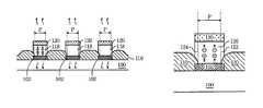
- FIG. 1is a schematic view of a basic structure of the organic light emitting diode (OLED) device.
- FIG. 2is a schematic view of depositing the emission layer on the surface of the electrode in accordance with the prior art.
- FIG. 3is a cross sectional view of the transparent substrate illustrating the steps of forming the first electrodes, the insulating layer, and the photo-resist layer in accordance with the present invention.
- FIG. 4is a cross sectional view of the transparent substrate illustrating the steps of defining apertures within the insulating layer.
- FIG. 5is a schematic view of depositing the emission layer on the surface of the electrode in accordance with the present invention.
- FIG. 6is a cross sectional view of the transparent substrate illustrating the steps of forming the second electrodes on the surface of the emission layer in accordance with the present invention.
- FIG. 7is a schematic view of the insulating layer which limits the emission region of the OLED device in accordance with the present invention.
- the invention disclosed hereinis an OLED structure including an insulating layer which functions to control the light emission region of each pixel thereby improving the uniformity of image manifestation.
- numerous detailsare set forth in order to provide a thorough understanding of the present invention. It will be appreciated by one skilled in the art that variations of these specific details are possible while still achieving the results of the present invention. In other instance, well-known components are not described in detail in order not to unnecessarily obscure the present invention.
- a plurality of first electrodes 102are formed on a transparent substrate 100 (e.g. of glass, plastic, or the like) by performing a PVD or CVD procedure such as sputtering, electron beam evaporation, thermal evaporation deposition, or spray pyrolysis.
- the conductive electrode layercan be chosen from metal such as magnesium(Mg), aluminum(Al), lithium(Li), alloy and any combination thereof or transparent conductive material such as indium-tin-oxide(ITO) and indium-zinc-oxide(IZO). Then performing a photolithography and an etching procedure for patterning the first electrodes 102 on the transparent substrate 100 .
- an insulating layer 104is deposited over the transparent substrate 100 and the first electrodes 102 .
- the insulating layer 104can be chosen from the group of oxide, nitride, or the like(e.g. of SiO 2 , SiN x and SiON).
- the insulating layer 104is formed of silicon oxide layer by applying a chemical vapor deposition(CVD) process.
- CVDchemical vapor deposition
- a photo-resist layeris coated on the insulating layer 104 .
- the photo-resist layeris precisely defined by exposing and developing procedures to form photo-resist pattern 106 on the insulating layer 104 . Such that the aperture regions 108 with predetermined size “P” are formed within the photo-resist pattern 106 .
- the photo-resist pattern 106is applied to serve as an etching mask for performing an anisotropic etch to the insulating layer 104 .
- the aperture regions 108are formed within the insulating layer 104 and then each central portion of first electrodes 102 are exposed.
- the insulating layer 110is defined with several aperture regions 108 and each one has a predetermined size “P.”
- removing the photo-resist pattern 106as shown in FIG. 4 .
- an emission layer 118is deposited in blanket form over substantially the entire substrate.
- the emission layer 118is an organic electroluminescent medium which can be chosen from the group of Alq, DPT, DCM-2, TMS-SiPc, TPAN, DPAN and TTBND/BTX-1, etc.
- the steps of depositing the emission layer 118comprise of, turning over the substrate first, and then disposing a shadow mask 112 which has been defined with several holes 114 beneath the substrate. Each hole 114 has a predetermined size “S”.
- the organic material 116can be coated through the holes 114 and onto the first electrodes 102 .
- the deposition methodcan be selected from Electron Beam Evaporation, Thermal Evaporation, Dip Coating, Spin Coating, Langmuir-Blodgett method and Sol-Gel method, etc.
- each hole 114has been defined with same predetermined size “S.” But, in real case, each hole 114 might have different sizes(e.g. S 1 ′ ⁇ grave over ( ) ⁇ S 2 ′ ⁇ grave over ( ) ⁇ S 3 ′ as illustrated in FIG. 5 ). Unavoidably, the size of the emission layer 118 which is deposited through the holes 114 must change too(e.g. S 1 ′ ⁇ grave over ( ) ⁇ S 2 ′ ⁇ grave over ( ) ⁇ S 3 ′ as illustrated in FIG. 5 ).
- the second electrodes 120are deposited on the emission layer 118 , as shown in FIG. 6 .
- the conductive electrode layercan be chosen from metal such as magnesium(Mg), aluminum(Al), lithium(Li), alloy and any combination thereof or transparent conductive material such as indium-tin-oxide(ITO) and indium-zinc-oxide(IZO). Then performing a photolithography and an etching procedure for patterning the second electrodes 120 on the emission layer 118 .
Landscapes
- Engineering & Computer Science (AREA)
- Microelectronics & Electronic Packaging (AREA)
- Electroluminescent Light Sources (AREA)
Abstract
Description
(1) Field of the Invention
The invention relates to an organic light emitting diode (OLED) display, and a method of making same. More particularly, this invention relates to an OLED structure including an insulating layer which functions to control the light emission region of each pixel thereby improving the uniformity of image manifestation.
(2) Description of the Prior Art
Owing to high brightness, fast response speed, light weight, thin and small features, full color, no viewing angle differences, no need for an LCD back-light board and low electrical consumption, an organic light emitting diode display or organic electroluminescence display (OLED) takes the lead to substitute a twist nematic (TN) or a super twist nematic (STN) liquid crystal display. Further, it substitutes for a small-sized thin-film transistor (TFT) LCD to become a new display material of fabricating portable information products, cell phones, personal digital assistant (PDA) and notebook.
Conventional OLED display structures are built on glass substrate in a manner such that a two-dimensional OLED array for image manifestation is formed. Each OLED in the array, referring toFIG. 1 , generally includes overlaying layers starting with a light transmissivefirst electrode 12 formed on the substrate, an organic electroluminescent (EL)emission medium 10 deposited over thefirst electrode 12, and ametallic electrode 14 on top of the organicelectroluminescent emission medium 10. When an electrical potential is placed across the electrodes, holes and electrons are injected into the organic zones from the anode and cathode, respectively. Light emission results from hole-electron recombination within the device.
As shown inFIG. 2 , conventionally, the first step for manufacturing OLED display is to evaporate or sputter light transmissive first electrodes102 (e.g. of indium-tin-oxide or ITO) on aglass substrate 100. Then an emission layer116 (e.g. of organic electroluminescent medium) is evaporated on theelectrode 102 by using ashadow mask 112 which has been defined holes thereon. This is because all the holes have same size “T” that all the emission layer blocks have same size. However, the realistic condition is theshadow mask 112 may droop causing of temperature, weight, etc. Then each hole may not have same size (e.g. T1′{grave over ( )}T2′{grave over ( )}T3′ as shown inFIG. 2 ) that the emission layer blocks result to different size. Consequently, each pixel of light emission region is changed and result in a problem of non-uniformity and bad quality of image manifestation. Thus, to solve the above-mentioned problem is the most important issue nowadays.
It is a purpose of this invention to fulfill the above described needs in the art, as well as other needs which will become apparent to the skilled artisan from the following detailed description of this invention.
The primary objective of the present invention is to provide an organic light emitting diode display device with an insulating layer to precisely control the light emission region and improving the uniformity of image manifestation.
The present invention is directed to an organic light emitting diode display having an insulating layer to function as a shelter. Before the steps of depositing the emission layer, defining an insulating layer for controlling the light emission region. Then even if every size of the organic layer is evaporated over the first electrodes are changed. The light emission region is limited by the predetermined size precisely controlled by the insulating layer so as to maintain the uniformity of image manifestation.
In manufacturing the present invention, the first electrodes are deposited and patterned on the substrate firstly. Next, the insulating layer is deposited over the first electrodes on the substrate. Then an etching procedure is done to etch the insulating layer for defining several predetermined apertures to expose each central portion of first electrodes. Subsequently, the emission layer is deposited above the substrate to cover the first electrodes. Finally, the second electrodes are deposited and patterned on the emission layer. This is because the insulating layer covers partial first electrodes that the light emitting of the emission layer is limited by and equal to predetermined apertures.
The present invention will now be specified with reference to its preferred embodiment illustrated in the drawings, in which
The invention disclosed herein is an OLED structure including an insulating layer which functions to control the light emission region of each pixel thereby improving the uniformity of image manifestation. In the following description, numerous details are set forth in order to provide a thorough understanding of the present invention. It will be appreciated by one skilled in the art that variations of these specific details are possible while still achieving the results of the present invention. In other instance, well-known components are not described in detail in order not to unnecessarily obscure the present invention.
Referring toFIG. 3 , in the present invention, a plurality offirst electrodes 102 are formed on a transparent substrate100 (e.g. of glass, plastic, or the like) by performing a PVD or CVD procedure such as sputtering, electron beam evaporation, thermal evaporation deposition, or spray pyrolysis. And the conductive electrode layer can be chosen from metal such as magnesium(Mg), aluminum(Al), lithium(Li), alloy and any combination thereof or transparent conductive material such as indium-tin-oxide(ITO) and indium-zinc-oxide(IZO). Then performing a photolithography and an etching procedure for patterning thefirst electrodes 102 on thetransparent substrate 100.
Subsequently, aninsulating layer 104 is deposited over thetransparent substrate 100 and thefirst electrodes 102. In general, theinsulating layer 104 can be chosen from the group of oxide, nitride, or the like(e.g. of SiO2, SiNxand SiON). In a preferred embodiment, theinsulating layer 104 is formed of silicon oxide layer by applying a chemical vapor deposition(CVD) process. Then a photo-resist layer is coated on theinsulating layer 104. And the photo-resist layer is precisely defined by exposing and developing procedures to form photo-resist pattern 106 on theinsulating layer 104. Such that theaperture regions 108 with predetermined size “P” are formed within the photo-resist pattern 106.
Then the photo-resist pattern 106 is applied to serve as an etching mask for performing an anisotropic etch to the insulatinglayer 104. Such that theaperture regions 108 are formed within theinsulating layer 104 and then each central portion offirst electrodes 102 are exposed. And theinsulating layer 110 is defined withseveral aperture regions 108 and each one has a predetermined size “P.” Next, removing the photo-resist pattern 106, as shown in FIG.4.
After theaperture regions 108 have been formed, anemission layer 118 is deposited in blanket form over substantially the entire substrate. And theemission layer 118 is an organic electroluminescent medium which can be chosen from the group of Alq, DPT, DCM-2, TMS-SiPc, TPAN, DPAN and TTBND/BTX-1, etc. The steps of depositing theemission layer 118 comprise of, turning over the substrate first, and then disposing ashadow mask 112 which has been defined withseveral holes 114 beneath the substrate. Eachhole 114 has a predetermined size “S”. As the deposition is proceeding, theorganic material 116 can be coated through theholes 114 and onto thefirst electrodes 102. However, the deposition method can be selected from Electron Beam Evaporation, Thermal Evaporation, Dip Coating, Spin Coating, Langmuir-Blodgett method and Sol-Gel method, etc.
Owing to theshadow mask 112 might droop causing of temperature or weight such that everyhole 114 formed thereon might change their size too. Originally, eachhole 114 has been defined with same predetermined size “S.” But, in real case, eachhole 114 might have different sizes(e.g. S1′{grave over ( )}S2′{grave over ( )}S3′ as illustrated in FIG.5). Unavoidably, the size of theemission layer 118 which is deposited through theholes 114 must change too(e.g. S1′{grave over ( )}S2′{grave over ( )}S3′ as illustrated in FIG.5).
Eventually, thesecond electrodes 120 are deposited on theemission layer 118, as shown in FIG.6. And the conductive electrode layer can be chosen from metal such as magnesium(Mg), aluminum(Al), lithium(Li), alloy and any combination thereof or transparent conductive material such as indium-tin-oxide(ITO) and indium-zinc-oxide(IZO). Then performing a photolithography and an etching procedure for patterning thesecond electrodes 120 on theemission layer 118.
Referring toFIG. 7 , as applying an electrical potential between thefirst electrode 102 and thesecond electrode 120, holes and electrons are injected into the organic zone from the anode and cathode, respectively. Light emission results from hole-electron recombination within the organic zone. At this moment, the portions of the organic medium coated on the insulatinglayer 110 are blocked by the insulatinglayer 110 that these region will lack of the hole-electron recombination phenomenon. Without the recombination phenomenon no light emitting are occurred from theseregion light emission region 126 is limited in the predetermined size “P” which is controlled by the insulatinglayer 110 as shown in FIG.7.
The foregoing is illustrative of the present invention and is not to be construed as limiting thereof. Although a few exemplary embodiments of this invention have been described, those skilled in the art will readily appreciate that many modifications are possible in the exemplary embodiments without materially departing from the novel teachings and advantages of this invention. Accordingly, all such modifications are intended to be included within the scope of this invention as defined in the claims. Therefore, it is to be understood that the foregoing is illustrative of the present invention and is not to be construed as limited to the specific embodiments disclosed, and that modifications to the disclosed embodiments, as will as other embodiments, are intended to be included within the scope of the appended claims. The invention is defined by the following claims, with equivalents of the claims to be included therein.
Claims (13)
1. An organic light emitting diode (OLED) comprising:
a transparent substrate;
a plurality of first electrodes provided on said transparent substrate;
an insulating layer provided on said plurality of first electrodes and said transparent substrate, wherein said insulating layer has a plurality of predetermined apertures to expose each central portion of said plurality of first electrodes;
an emission layer provided on said insulating layer and filled up said plurality of predetermined apertures thereof; and
a plurality of second electrodes provided on said emission layer;
wherein said insulating layer covers partial said plurality of first electrodes that the light emitting of said emission layer is limited by and equal to said plurality of predetermined apertures.
2. The OLED ofclaim 1 , wherein the transparent substrate is made of a plastic.
3. The OLED ofclaim 1 , wherein the transparent substrate is made of a glass.
4. The OLED ofclaim 1 , wherein said plurality of first electrodes and said plurality of second electrodes are selected from the group consisting of ITO and IZO.
5. The OLED ofclaim 1 , wherein said plurality of first electrodes and said plurality of second electrodes are selected from the group consisting of Mg, Li and Al.
6. The OLED ofclaim 1 , wherein said insulating layer is selected from the group consisting of SiO2, SiNxand SiON.
7. The OLED ofclaim 1 , wherein said emission layer is selected from the group consisting of Alq, DPT, DCM-2, TMS-SiPc, TPAN, DPAN and TTBND/BTX-1.
8. A method of manufacturing an organic light emitting diode (OLED), the method comprises the following steps of:
providing a transparent substrate;
depositing and patterning a plurality of first electrodes on said transparent substrate;
depositing an insulating layer on said plurality of first electrodes and said transparent substrate;
performing an etching procedure to said insulating layer for defining a plurality of predetermined apertures thereon to expose each central portion of said plurality of first electrodes;
depositing an emission layer to cover said plurality of first electrodes; and
depositing and patterning a plurality of second electrodes on said emission layer;
wherein said insulating layer covers partial said plurality of first electrodes that the light emitting of said emission layer is limited by and equal to said plurality of predetermined apertures.
9. The method ofclaim 8 , wherein said etching procedure further comprises the steps of:
depositing and patterning a photo-resist layer on said insulating layer for defining said plurality of predetermined apertures;
etching said insulating layer by using said photo-resist layer as a mask for removing partial said insulating layer; and
removing said photo-resist layer.
10. The method ofclaim 8 , wherein said steps of depositing said emission layer is through a shadow mask.
11. The method ofclaim 10 , wherein said steps of depositing method is selected from the group consisting of Electron Beam Evaporation, Thermal Evaporation, Dip Coating, Spin Coating, Langmuir-Blodgett method and Sol-Gel method.
12. The method ofclaim 8 , wherein said steps of depositing said plurality of first electrodes and said plurality of second electrodes are performed by a method selected from the group consisting of Sputtering, Electron Beam Evaporation, Thermal Evaporation Deposition, Chemical Vapor Deposition and Spray Pyrolysis.
13. The method ofclaim 8 , wherein said emission layer covers said insulating layer which is around said plurality of first electrodes.
Applications Claiming Priority (2)
| Application Number | Priority Date | Filing Date | Title |
|---|---|---|---|
| TW92101265 | 2003-01-21 | ||
| TW092101265ATW200414824A (en) | 2003-01-21 | 2003-01-21 | Organic light emitting diode flat display with an insulating layer for shielding |
Publications (2)
| Publication Number | Publication Date |
|---|---|
| US20040140761A1 US20040140761A1 (en) | 2004-07-22 |
| US6844675B2true US6844675B2 (en) | 2005-01-18 |
Family
ID=32710203
Family Applications (1)
| Application Number | Title | Priority Date | Filing Date |
|---|---|---|---|
| US10/446,102Expired - LifetimeUS6844675B2 (en) | 2003-01-21 | 2003-05-28 | Organic light emitting diode display with an insulating layer as a shelter |
Country Status (2)
| Country | Link |
|---|---|
| US (1) | US6844675B2 (en) |
| TW (1) | TW200414824A (en) |
Cited By (9)
| Publication number | Priority date | Publication date | Assignee | Title |
|---|---|---|---|---|
| US11284491B2 (en) | 2011-12-02 | 2022-03-22 | Lynk Labs, Inc. | Color temperature controlled and low THD LED lighting devices and systems and methods of driving the same |
| US11297705B2 (en) | 2007-10-06 | 2022-04-05 | Lynk Labs, Inc. | Multi-voltage and multi-brightness LED lighting devices and methods of using same |
| US11317495B2 (en) | 2007-10-06 | 2022-04-26 | Lynk Labs, Inc. | LED circuits and assemblies |
| US11528792B2 (en) | 2004-02-25 | 2022-12-13 | Lynk Labs, Inc. | High frequency multi-voltage and multi-brightness LED lighting devices |
| US11566759B2 (en) | 2017-08-31 | 2023-01-31 | Lynk Labs, Inc. | LED lighting system and installation methods |
| US11638336B2 (en) | 2004-02-25 | 2023-04-25 | Lynk Labs, Inc. | AC light emitting diode and AC LED drive methods and apparatus |
| US11678420B2 (en) | 2004-02-25 | 2023-06-13 | Lynk Labs, Inc. | LED lighting system |
| US11953167B2 (en) | 2011-08-18 | 2024-04-09 | Lynk Labs, Inc. | Devices and systems having AC LED circuits and methods of driving the same |
| US12279345B2 (en) | 2009-12-28 | 2025-04-15 | Lynk Labs, Inc. | Light emitting diode and LED drive apparatus |
Families Citing this family (3)
| Publication number | Priority date | Publication date | Assignee | Title |
|---|---|---|---|---|
| US20060021869A1 (en)* | 2004-07-28 | 2006-02-02 | Advantech Global, Ltd | System for and method of ensuring accurate shadow mask-to-substrate registration in a deposition process |
| JP5410127B2 (en)* | 2009-03-24 | 2014-02-05 | 山本化成株式会社 | Organic transistor |
| CN109599030B (en)* | 2017-09-30 | 2020-12-11 | 昆山国显光电有限公司 | Display screen and electronic product |
Citations (1)
| Publication number | Priority date | Publication date | Assignee | Title |
|---|---|---|---|---|
| US6429580B1 (en)* | 1995-10-13 | 2002-08-06 | Canon Kabushiki Kaisha | Methods of manufacturing electron-emitting device, electron source and image forming apparatus |
- 2003
- 2003-01-21TWTW092101265Apatent/TW200414824A/enunknown
- 2003-05-28USUS10/446,102patent/US6844675B2/ennot_activeExpired - Lifetime
Patent Citations (1)
| Publication number | Priority date | Publication date | Assignee | Title |
|---|---|---|---|---|
| US6429580B1 (en)* | 1995-10-13 | 2002-08-06 | Canon Kabushiki Kaisha | Methods of manufacturing electron-emitting device, electron source and image forming apparatus |
Cited By (14)
| Publication number | Priority date | Publication date | Assignee | Title |
|---|---|---|---|---|
| US11678420B2 (en) | 2004-02-25 | 2023-06-13 | Lynk Labs, Inc. | LED lighting system |
| US11528792B2 (en) | 2004-02-25 | 2022-12-13 | Lynk Labs, Inc. | High frequency multi-voltage and multi-brightness LED lighting devices |
| US11638336B2 (en) | 2004-02-25 | 2023-04-25 | Lynk Labs, Inc. | AC light emitting diode and AC LED drive methods and apparatus |
| US11729884B2 (en) | 2007-10-06 | 2023-08-15 | Lynk Labs, Inc. | LED circuits and assemblies |
| US11317495B2 (en) | 2007-10-06 | 2022-04-26 | Lynk Labs, Inc. | LED circuits and assemblies |
| US11297705B2 (en) | 2007-10-06 | 2022-04-05 | Lynk Labs, Inc. | Multi-voltage and multi-brightness LED lighting devices and methods of using same |
| US12213224B2 (en) | 2007-10-06 | 2025-01-28 | Lynk Labs, Inc. | Multi-voltage and multi-brightness LED lighting devices and methods of using same |
| US12279345B2 (en) | 2009-12-28 | 2025-04-15 | Lynk Labs, Inc. | Light emitting diode and LED drive apparatus |
| US11953167B2 (en) | 2011-08-18 | 2024-04-09 | Lynk Labs, Inc. | Devices and systems having AC LED circuits and methods of driving the same |
| US12435847B2 (en) | 2011-08-18 | 2025-10-07 | Lynk Labs, Inc. | Devices and systems having LED circuits and methods of driving the same |
| US11284491B2 (en) | 2011-12-02 | 2022-03-22 | Lynk Labs, Inc. | Color temperature controlled and low THD LED lighting devices and systems and methods of driving the same |
| US12028947B2 (en) | 2011-12-02 | 2024-07-02 | Lynk Labs, Inc. | Color temperature controlled and low THD LED lighting devices and systems and methods of driving the same |
| US11566759B2 (en) | 2017-08-31 | 2023-01-31 | Lynk Labs, Inc. | LED lighting system and installation methods |
| US12104766B2 (en) | 2017-08-31 | 2024-10-01 | Lynk Labs, Inc. | LED lighting system and installation methods |
Also Published As
| Publication number | Publication date |
|---|---|
| US20040140761A1 (en) | 2004-07-22 |
| TW200414824A (en) | 2004-08-01 |
Similar Documents
| Publication | Publication Date | Title |
|---|---|---|
| CN109244269B (en) | Display panel, manufacturing method thereof and display device | |
| US6582888B1 (en) | Method for producing organic electroluminescent components | |
| US9496511B2 (en) | Organic semiconductor thin film transistor and method of fabricating the same | |
| US20220376007A1 (en) | Display substrate, method for forming the same and display device | |
| US9722005B2 (en) | Light-emitting device, array substrate, display device and manufacturing method of light-emitting device | |
| JP5642142B2 (en) | Thin film transistor, thin film transistor array substrate, and manufacturing method thereof | |
| US7947518B2 (en) | Method for forming electronic devices by using protecting layers | |
| US8294362B2 (en) | Image display device, image display system, and methods for fabricating the same | |
| US8951700B2 (en) | Methods of manufacturing optical filters and methods of manufacturing organic light emitting display devices having optical filters | |
| US6844675B2 (en) | Organic light emitting diode display with an insulating layer as a shelter | |
| US11245087B2 (en) | Display substrate and its manufacturing method | |
| US20160027813A1 (en) | Array substrate and manufacturing method thereof and display apparatus | |
| US20040178724A1 (en) | Display panel and electronic apparatus with the same | |
| CN109742125A (en) | Fabrication method of array substrate, array substrate, display panel and display device | |
| CN108231857B (en) | OLED microcavity structure and preparation method thereof, and display device | |
| US20070102714A1 (en) | Display device and manufacturing method thereof | |
| US20110168985A1 (en) | Organic Light Emitting Diode Display Device and Method of Manufacturing the Same | |
| KR20080049910A (en) | Organic light emitting display device and manufacturing method thereof | |
| US20050231103A1 (en) | Flat panel display device and method for manufacturing the same | |
| US11362155B2 (en) | Display substrate, manufacturing method thereof and display device | |
| US20060197441A1 (en) | Array substrates for electroluminescent displays and methods of forming the same | |
| US20220123252A1 (en) | Display substrate and manufacturing method thereof, display panel and display device | |
| CN100481485C (en) | Method for fabricating organic electro-luminance device | |
| KR100848342B1 (en) | Manufacturing method of organic electroluminescent display | |
| US12336393B2 (en) | Light-emitting device, substrate thereof and fabrication method |
Legal Events
| Date | Code | Title | Description |
|---|---|---|---|
| AS | Assignment | Owner name:AU OPTRONICS CORP., TAIWAN Free format text:ASSIGNMENT OF ASSIGNORS INTEREST;ASSIGNOR:YANG, CHIEN-SHENG;REEL/FRAME:014126/0850 Effective date:20030515 | |
| STCF | Information on status: patent grant | Free format text:PATENTED CASE | |
| FPAY | Fee payment | Year of fee payment:4 | |
| FPAY | Fee payment | Year of fee payment:8 | |
| FPAY | Fee payment | Year of fee payment:12 | |
| AS | Assignment | Owner name:TESCOM CO., LTD., JAPAN Free format text:ASSIGNMENT OF ASSIGNORS INTEREST;ASSIGNOR:AU OPTRONICS CORPORATION;REEL/FRAME:059896/0532 Effective date:20211229 | |
| AS | Assignment | Owner name:XIAMEN TIANMA DISPLAY TECHNOLOGY CO., LTD., CHINA Free format text:ASSIGNMENT OF ASSIGNORS INTEREST;ASSIGNOR:TESCOM CO., LTD.;REEL/FRAME:064491/0623 Effective date:20230602 |