US6844604B2 - Dielectric layer for semiconductor device and method of manufacturing the same - Google Patents
Dielectric layer for semiconductor device and method of manufacturing the sameDownload PDFInfo
- Publication number
- US6844604B2 US6844604B2US09/776,059US77605901AUS6844604B2US 6844604 B2US6844604 B2US 6844604B2US 77605901 AUS77605901 AUS 77605901AUS 6844604 B2US6844604 B2US 6844604B2
- Authority
- US
- United States
- Prior art keywords
- layer
- dielectric
- silicate
- silicate interface
- metal
- Prior art date
- Legal status (The legal status is an assumption and is not a legal conclusion. Google has not performed a legal analysis and makes no representation as to the accuracy of the status listed.)
- Expired - Lifetime, expires
Links
Images


Classifications
- H—ELECTRICITY
- H01—ELECTRIC ELEMENTS
- H01L—SEMICONDUCTOR DEVICES NOT COVERED BY CLASS H10
- H01L21/00—Processes or apparatus adapted for the manufacture or treatment of semiconductor or solid state devices or of parts thereof
- H01L21/02—Manufacture or treatment of semiconductor devices or of parts thereof
- H01L21/04—Manufacture or treatment of semiconductor devices or of parts thereof the devices having potential barriers, e.g. a PN junction, depletion layer or carrier concentration layer
- H01L21/18—Manufacture or treatment of semiconductor devices or of parts thereof the devices having potential barriers, e.g. a PN junction, depletion layer or carrier concentration layer the devices having semiconductor bodies comprising elements of Group IV of the Periodic Table or AIIIBV compounds with or without impurities, e.g. doping materials
- H01L21/30—Treatment of semiconductor bodies using processes or apparatus not provided for in groups H01L21/20 - H01L21/26
- H01L21/31—Treatment of semiconductor bodies using processes or apparatus not provided for in groups H01L21/20 - H01L21/26 to form insulating layers thereon, e.g. for masking or by using photolithographic techniques; After treatment of these layers; Selection of materials for these layers
- H—ELECTRICITY
- H01—ELECTRIC ELEMENTS
- H01L—SEMICONDUCTOR DEVICES NOT COVERED BY CLASS H10
- H01L21/00—Processes or apparatus adapted for the manufacture or treatment of semiconductor or solid state devices or of parts thereof
- H01L21/02—Manufacture or treatment of semiconductor devices or of parts thereof
- H01L21/04—Manufacture or treatment of semiconductor devices or of parts thereof the devices having potential barriers, e.g. a PN junction, depletion layer or carrier concentration layer
- H01L21/18—Manufacture or treatment of semiconductor devices or of parts thereof the devices having potential barriers, e.g. a PN junction, depletion layer or carrier concentration layer the devices having semiconductor bodies comprising elements of Group IV of the Periodic Table or AIIIBV compounds with or without impurities, e.g. doping materials
- H01L21/28—Manufacture of electrodes on semiconductor bodies using processes or apparatus not provided for in groups H01L21/20 - H01L21/268
- H01L21/28008—Making conductor-insulator-semiconductor electrodes
- H01L21/28017—Making conductor-insulator-semiconductor electrodes the insulator being formed after the semiconductor body, the semiconductor being silicon
- H01L21/28158—Making the insulator
- H01L21/28167—Making the insulator on single crystalline silicon, e.g. using a liquid, i.e. chemical oxidation
- H01L21/28185—Making the insulator on single crystalline silicon, e.g. using a liquid, i.e. chemical oxidation with a treatment, e.g. annealing, after the formation of the gate insulator and before the formation of the definitive gate conductor
- H—ELECTRICITY
- H01—ELECTRIC ELEMENTS
- H01L—SEMICONDUCTOR DEVICES NOT COVERED BY CLASS H10
- H01L21/00—Processes or apparatus adapted for the manufacture or treatment of semiconductor or solid state devices or of parts thereof
- H01L21/02—Manufacture or treatment of semiconductor devices or of parts thereof
- H01L21/04—Manufacture or treatment of semiconductor devices or of parts thereof the devices having potential barriers, e.g. a PN junction, depletion layer or carrier concentration layer
- H01L21/18—Manufacture or treatment of semiconductor devices or of parts thereof the devices having potential barriers, e.g. a PN junction, depletion layer or carrier concentration layer the devices having semiconductor bodies comprising elements of Group IV of the Periodic Table or AIIIBV compounds with or without impurities, e.g. doping materials
- H01L21/28—Manufacture of electrodes on semiconductor bodies using processes or apparatus not provided for in groups H01L21/20 - H01L21/268
- H01L21/28008—Making conductor-insulator-semiconductor electrodes
- H01L21/28017—Making conductor-insulator-semiconductor electrodes the insulator being formed after the semiconductor body, the semiconductor being silicon
- H01L21/28158—Making the insulator
- H01L21/28167—Making the insulator on single crystalline silicon, e.g. using a liquid, i.e. chemical oxidation
- H01L21/28194—Making the insulator on single crystalline silicon, e.g. using a liquid, i.e. chemical oxidation by deposition, e.g. evaporation, ALD, CVD, sputtering, laser deposition
- H—ELECTRICITY
- H01—ELECTRIC ELEMENTS
- H01L—SEMICONDUCTOR DEVICES NOT COVERED BY CLASS H10
- H01L21/00—Processes or apparatus adapted for the manufacture or treatment of semiconductor or solid state devices or of parts thereof
- H01L21/02—Manufacture or treatment of semiconductor devices or of parts thereof
- H01L21/04—Manufacture or treatment of semiconductor devices or of parts thereof the devices having potential barriers, e.g. a PN junction, depletion layer or carrier concentration layer
- H01L21/18—Manufacture or treatment of semiconductor devices or of parts thereof the devices having potential barriers, e.g. a PN junction, depletion layer or carrier concentration layer the devices having semiconductor bodies comprising elements of Group IV of the Periodic Table or AIIIBV compounds with or without impurities, e.g. doping materials
- H01L21/28—Manufacture of electrodes on semiconductor bodies using processes or apparatus not provided for in groups H01L21/20 - H01L21/268
- H01L21/28008—Making conductor-insulator-semiconductor electrodes
- H01L21/28017—Making conductor-insulator-semiconductor electrodes the insulator being formed after the semiconductor body, the semiconductor being silicon
- H01L21/28158—Making the insulator
- H01L21/28167—Making the insulator on single crystalline silicon, e.g. using a liquid, i.e. chemical oxidation
- H01L21/28202—Making the insulator on single crystalline silicon, e.g. using a liquid, i.e. chemical oxidation in a nitrogen-containing ambient, e.g. nitride deposition, growth, oxynitridation, NH3 nitridation, N2O oxidation, thermal nitridation, RTN, plasma nitridation, RPN
- H—ELECTRICITY
- H10—SEMICONDUCTOR DEVICES; ELECTRIC SOLID-STATE DEVICES NOT OTHERWISE PROVIDED FOR
- H10D—INORGANIC ELECTRIC SEMICONDUCTOR DEVICES
- H10D1/00—Resistors, capacitors or inductors
- H10D1/60—Capacitors
- H10D1/62—Capacitors having potential barriers
- H10D1/66—Conductor-insulator-semiconductor capacitors, e.g. MOS capacitors
- H—ELECTRICITY
- H10—SEMICONDUCTOR DEVICES; ELECTRIC SOLID-STATE DEVICES NOT OTHERWISE PROVIDED FOR
- H10D—INORGANIC ELECTRIC SEMICONDUCTOR DEVICES
- H10D30/00—Field-effect transistors [FET]
- H10D30/60—Insulated-gate field-effect transistors [IGFET]
- H10D30/68—Floating-gate IGFETs
- H10D30/681—Floating-gate IGFETs having only two programming levels
- H—ELECTRICITY
- H10—SEMICONDUCTOR DEVICES; ELECTRIC SOLID-STATE DEVICES NOT OTHERWISE PROVIDED FOR
- H10D—INORGANIC ELECTRIC SEMICONDUCTOR DEVICES
- H10D64/00—Electrodes of devices having potential barriers
- H10D64/60—Electrodes characterised by their materials
- H10D64/66—Electrodes having a conductor capacitively coupled to a semiconductor by an insulator, e.g. MIS electrodes
- H10D64/68—Electrodes having a conductor capacitively coupled to a semiconductor by an insulator, e.g. MIS electrodes characterised by the insulator, e.g. by the gate insulator
- H10D64/681—Electrodes having a conductor capacitively coupled to a semiconductor by an insulator, e.g. MIS electrodes characterised by the insulator, e.g. by the gate insulator having a compositional variation, e.g. multilayered
- H10D64/685—Electrodes having a conductor capacitively coupled to a semiconductor by an insulator, e.g. MIS electrodes characterised by the insulator, e.g. by the gate insulator having a compositional variation, e.g. multilayered being perpendicular to the channel plane
- H—ELECTRICITY
- H10—SEMICONDUCTOR DEVICES; ELECTRIC SOLID-STATE DEVICES NOT OTHERWISE PROVIDED FOR
- H10D—INORGANIC ELECTRIC SEMICONDUCTOR DEVICES
- H10D64/00—Electrodes of devices having potential barriers
- H10D64/60—Electrodes characterised by their materials
- H10D64/66—Electrodes having a conductor capacitively coupled to a semiconductor by an insulator, e.g. MIS electrodes
- H10D64/68—Electrodes having a conductor capacitively coupled to a semiconductor by an insulator, e.g. MIS electrodes characterised by the insulator, e.g. by the gate insulator
- H10D64/691—Electrodes having a conductor capacitively coupled to a semiconductor by an insulator, e.g. MIS electrodes characterised by the insulator, e.g. by the gate insulator comprising metallic compounds, e.g. metal oxides or metal silicates
- H—ELECTRICITY
- H10—SEMICONDUCTOR DEVICES; ELECTRIC SOLID-STATE DEVICES NOT OTHERWISE PROVIDED FOR
- H10D—INORGANIC ELECTRIC SEMICONDUCTOR DEVICES
- H10D64/00—Electrodes of devices having potential barriers
- H10D64/60—Electrodes characterised by their materials
- H10D64/66—Electrodes having a conductor capacitively coupled to a semiconductor by an insulator, e.g. MIS electrodes
- H10D64/68—Electrodes having a conductor capacitively coupled to a semiconductor by an insulator, e.g. MIS electrodes characterised by the insulator, e.g. by the gate insulator
- H10D64/693—Electrodes having a conductor capacitively coupled to a semiconductor by an insulator, e.g. MIS electrodes characterised by the insulator, e.g. by the gate insulator the insulator comprising nitrogen, e.g. nitrides, oxynitrides or nitrogen-doped materials
- H—ELECTRICITY
- H10—SEMICONDUCTOR DEVICES; ELECTRIC SOLID-STATE DEVICES NOT OTHERWISE PROVIDED FOR
- H10D—INORGANIC ELECTRIC SEMICONDUCTOR DEVICES
- H10D1/00—Resistors, capacitors or inductors
- H10D1/60—Capacitors
- H10D1/68—Capacitors having no potential barriers
- H10D1/682—Capacitors having no potential barriers having dielectrics comprising perovskite structures
- H10D1/684—Capacitors having no potential barriers having dielectrics comprising perovskite structures the dielectrics comprising multiple layers, e.g. comprising buffer layers, seed layers or gradient layers
Definitions
- a thermal oxide layere.g. silicon dioxide (SiO 2 )
- SiO 2silicon dioxide
- U.S. Pat. No. 6,020,024discloses an oxynitride layer interposed between a silicon substrate and a high-k dielectric layer.
- U.S. Pat. No. 6,013,553discloses a zirconium oxynitride layer or a hafnium oxynitride layer as the gate dielectrics.
- PCT International Patent Application Publication No. WO 00/01008discloses SiO 2 , silicon nitride and oxynitride interface layers.
- U.S. Pat. No. 6,020,243discloses a high permittivity zirconium (or hafnium) silicon-oxynitride gate dielectrics.
- the silicate interface layeris formed of a metal silicate material (M 1-x Si x O 2 ) and the metal “M” can be hafnium (Hf), zirconium (Zr), tantalum (Ta), titanium (Ti) or aluminum (Al).
- M 1-x Si x O 2metal silicate material
- the metal “M”can be hafnium (Hf), zirconium (Zr), tantalum (Ta), titanium (Ti) or aluminum (Al).
- interface characteristicscan be improved and the EOT can be maintained or reduced.
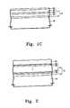
- FIG. 1Cis a cross-sectional view of a semiconductor device according to a further embodiment of the present invention.
- FIG. 2is a cross-sectional view of a semiconductor device according to yet another embodiment of the present invention.
- the present inventionprovides a noble dielectric layer structure and a method of manufacturing the same.
- numerous specific detailsare set forth to provide a thorough understanding of the present invention. However, one having ordinary skill in the art should recognize that the invention can be practiced without these specific details. In some instances, well-known process steps, device structures, and techniques have not been shown in detail to avoid obscuring the present invention.
- the present inventionis equally applicable to any dielectric for semiconductor devices, such as an inter-gate dielectric layer of non-volatile memory devices, or a dielectric layer of a storage capacitor, all of which are within the spirit and scope of the present invention.
- the silicate interface layer 12substantially improves interface characteristics.
- the silicate interface layer 12substantially prevents the reaction between the high-k dielectric layer 14 and the semiconductor substrate 10 . Because the silicate interface layer 12 is chemically stable when formed on silicon, an unnecessary interface layer such as silicon dioxide that would undesirably increases EOT substantially would not form.
- the metal of the silicate interface layer 12is preferably the same as the metal of the metal oxide layer (high-k dielectric layer 14 ).
- the dielectric layer structure 15comprises a hafnium silicate interface layer and a hafnium oxide layer, which are sequentially stacked.
- the upper most layer 22 (See FIG. 2 ) of the high-k dielectric layer 14be formed of Al 2 O 3 .
- the heat of formation of the Al 2 O 3 layeris greater than that of the ZrO 2 layer or the HfO 2 layer.
- the heat of formation of the Al 2 O 3 layeris ⁇ 1678 kJ/mol
- the heat of formations of the ZrO 2 layer and the HfO 2are ⁇ 1100 kJ/mol and ⁇ 1122 kJ/mol, respectively.
- the Al 2 O 3 layerdoes not react with the polysilicon layer 24 . Therefore, in the present invention, it is possible to improve the interface characteristics between the high-k dielectric layer and the gate electrode.
- the thickness of the second layer 20is approximately one half the thickness of the first layer 18 because the amount of fixed charge in Al 2 O 3 is thought to be approximately two times more than that of HfO 2 or ZrO 2 .
- the total thickness of the second layer 20is preferably not more than one third of the total thickness of the high-k dielectric layer 14 . This is especially true if the second layer 20 is HfO 2 .
- the transconductance of the MOS structure including the Al 2 O 3 layeris still less than that of the reference MOS structure.
- the interface trap densitycan be calculated using a charge pumping current shown in FIG. 6 , which shows the charge pumping current of SiO 2 and Al 2 O 3 .
- the interface trap density of Al 2 O 3is greater than SiO 2 .
- Such interface trap densitycan be reduced by introducing the metal silicate interface layer 12 between the silicon substrate 10 and the high-k dielectric layer 14 .
- the present inventionprovides a dielectric layer structure having the advantages of silicon dioxide but without the disadvantages of the prior art.
Landscapes
- Engineering & Computer Science (AREA)
- Manufacturing & Machinery (AREA)
- Power Engineering (AREA)
- General Physics & Mathematics (AREA)
- Physics & Mathematics (AREA)
- Computer Hardware Design (AREA)
- Condensed Matter Physics & Semiconductors (AREA)
- Microelectronics & Electronic Packaging (AREA)
- Crystallography & Structural Chemistry (AREA)
- Chemical Kinetics & Catalysis (AREA)
- Chemical & Material Sciences (AREA)
- General Chemical & Material Sciences (AREA)
- Insulated Gate Type Field-Effect Transistor (AREA)
- Formation Of Insulating Films (AREA)
- Semiconductor Integrated Circuits (AREA)
- Semiconductor Memories (AREA)
- Non-Volatile Memory (AREA)
Abstract
Description
1. Field of the Invention
This invention relates generally to the field of semiconductor devices, and more particularly, to a dielectric layer structure and a method of manufacturing the same.
2. Description of the Related Art
With each generation of metal oxide semiconductor (MOS) integrated circuit (IC), the device dimensions have been continuously scaled down to provide for high-density and high-performance devices. Particularly, the thickness of gate dielectrics is made as small as possible because the drive current in a MOS field effect transistor (FET) increases with decreasing gate dielectric thickness. Thus, it has become increasingly important to provide extremely thin, reliable, and low-defect gate dielectrics for improving device performance.
For decades, a thermal oxide layer, e.g. silicon dioxide (SiO2), has been used as the gate dielectrics because the silicon dioxide thermal oxide layer is stable with the underlying silicon substrate and the fabrication process is relatively simple.
However, because the silicon dioxide gate dielectrics has a low dielectric constant (k), e.g., 3.9, further scaling down of silicon dioxide gate dielectric thickness has become more and more difficult, especially due to gate-to-channel leakage current through thin silicon dioxide gate dielectrics.
This leads to consideration of alternative dielectric materials that can be formed in a thicker layer than silicon dioxide but still produce the same or better device performance. The performance can be expressed as “equivalent oxide thickness (EOT).”
This is mainly because the physically thicker metal oxide can reduce gate-to-channel leakage current while the device performance is not adversely impacted. Further, if the dielectric layer can be made sufficiently thick, etching margin can be increased during the patterning of gate stacks. This increased etching margin prevents the silicon substrate from being exposed by the etching process for patterning the gate stacks.
To this end, a high-k (high dielectric constant) metal oxide materials have been proposed as the alternative dielectric materials for gate or capacitor dielectrics. Because the dielectric constant of a metal oxide material can be made greater than that of the silicon dioxide, a thicker metal oxide layer having a similar EOT can be deposited.
Unfortunately, the use of high-k metal oxide materials presents several problems when using traditional substrate materials such as silicon. The silicon can react with the high-k metal oxide or oxidize during deposition of the high-k metal oxide or subsequent thermal processes, thereby forming an interface layer of silicon dioxide. This increases the equivalent oxide thickness, thereby degrading device performance.
Further, an interface trap density between the high-k metal oxide layer and the silicon substrate is increased. Thus, the channel mobility of the carriers is reduced. This reduces the on/off current ratio of the MOS transistor, thereby degrading its switching characteristics.
Also, the high-k metal oxide layer such as a hafnium oxide (HfO2) layer or a zirconium oxide (ZrO2) layer has a relatively low crystallization temperature and is thermally unstable. Thus, the metal oxide layer can be easily crystallized during a subsequent thermal annealing process for activating the impurities injected into source/drain regions. This can form grain boundaries in the metal oxide layer through which current can pass. And the surface roughness of the metal oxide layer increases, deteriorating the leakage current characteristics. Further, the crystallization of the high-k metal oxide layer undesirably affects a subsequent alignment process due to irregular reflection of the light on an alignment key having the rough surface.
Various attempts have been made to address the above-mentioned problems. For example, U.S. Pat. No. 6,020,024 discloses an oxynitride layer interposed between a silicon substrate and a high-k dielectric layer. U.S. Pat. No. 6,013,553 discloses a zirconium oxynitride layer or a hafnium oxynitride layer as the gate dielectrics. Further, PCT International Patent Application Publication No. WO 00/01008 discloses SiO2, silicon nitride and oxynitride interface layers. Also, U.S. Pat. No. 6,020,243 discloses a high permittivity zirconium (or hafnium) silicon-oxynitride gate dielectrics.
However, such methods have not succeeded in solving the above-mentioned problems. For example, the silicon nitride layer or oxynitride layer between the high-k dielectric layer and the silicon substrate or the polysilicon gate electrode causes charge trapping with high interface state densities. Thus, such methods reduce channel mobility and degrade device performance. Further, the formation of the silicon nitride layer or the oxynitride layer requires a relatively large thermal budget.
Importantly, in the case of the silicon nitride layer, because the dielectric constant of silicon nitride is only about 1.5 times greater than that of silicon dioxide, it has been difficult to reduce an EOT, thus inhibiting the improvements in device performance.
Accordingly, a need still remains for an improved dielectric layer structure with a higher crystallization temperature and the method of manufacturing the same to improve the device performance by reducing the equivalent oxide thickness of the dielectric layer as well as improvement of the interface characteristics.
The present invention provides a multi-layer dielectric layer structure for a semiconductor device. The multi-layer dielectric layer structure comprises a silicate interface layer and a high-k dielectric layer overlying the silicate interface layer.
According to one preferred embodiment of the present invention, the high-k dielectric layer has a dielectric constant greater than that of the silicate interface layer.
Preferably, the silicate interface layer is formed of a metal silicate material (M1-xSixO2) and the metal “M” can be hafnium (Hf), zirconium (Zr), tantalum (Ta), titanium (Ti) or aluminum (Al).
Preferably, the high-k dielectric layer comprises a metal oxide layer. The metal oxide layer preferably comprises an HfO2layer, a ZrO2layer, a Ta2O3layer, an Al2O3layer, a TiO2layer, an Y2O3layer, or a BST layer, a PZT layer, or combinations thereof.
Preferably, the high-k dielectric layer comprises one or more ordered pairs of first and second layers.
Preferably, the first layer is formed of HfO2, Ta2O3, Y2O3or ZrO2and the second layer is formed of Al2O3.
According to one aspect of the present invention, the dielectric constant of the high-k dielectric layer can be optimized with a minimum net fixed charge.
Further, in accordance with the other aspect of the present invention, interface characteristics can be improved and the EOT can be maintained or reduced.
In addition, according to another aspect of the present invention, with a higher crystallization temperature realized by forming a multi-layer structure, each of whose layers is not more than the critical thickness, leakage current can be reduced, thereby improving device performance.
The foregoing and other objects, features and advantages of the invention will become more readily apparent from the following detailed description of a preferred embodiment of the invention that proceeds with reference to the accompanying drawings.
The present invention provides a noble dielectric layer structure and a method of manufacturing the same. In the following description, numerous specific details are set forth to provide a thorough understanding of the present invention. However, one having ordinary skill in the art should recognize that the invention can be practiced without these specific details. In some instances, well-known process steps, device structures, and techniques have not been shown in detail to avoid obscuring the present invention.
Although the invention is described in conjunction with gate dielectrics of a MOS transistor, the present invention is equally applicable to any dielectric for semiconductor devices, such as an inter-gate dielectric layer of non-volatile memory devices, or a dielectric layer of a storage capacitor, all of which are within the spirit and scope of the present invention.
The preferred embodiments of the present invention are best understood by referring toFIGS. 1-7 of the drawings, in which like reference designators are used for like features.
Referring toFIGS. 1A-1C , according to the preferred embodiments of the present invention, asilicate interface layer 12 formed of a silicate material is deposited on asemiconductor substrate 10, e.g. a silicon substrate. The thickness of thesilicate interface layer 12 is preferably in the range of approximately 5-10 angstroms. The dielectric constant of thesilicate interface layer 12 is preferably greater than that of silicon nitride or oxynitride.
Then, a high-k dielectric layer 14 is formed on thesilicate interface layer 12. The high-k dielectric layer 14 has a dielectric constant higher than that of SiO2. Preferably, the high-k dielectric layer 14 has a dielectric constant greater than that of thesilicate interface layer 12.
Here, thesilicate interface layer 12 is preferably formed of metal silicate materials (M1-xSixO2). Here, the metal “M” can be hafnium (Hf), zirconium (Zr), tantalum (Ta), titanium (Ti) or aluminum (Al). However, this list is not intended to be exhaustive or to limit the invention. Any other material suitable for the present invention can be used within the sprit and scope of the present invention.
Thesilicate interface layer 12 substantially improves interface characteristics. For example, thesilicate interface layer 12 substantially prevents the reaction between the high-k dielectric layer 14 and thesemiconductor substrate 10. Because thesilicate interface layer 12 is chemically stable when formed on silicon, an unnecessary interface layer such as silicon dioxide that would undesirably increases EOT substantially would not form.
Also, it is believed that the present invention reduces the interface trap density contrasted with the prior art methods. This will be further explained in the below description, by reference toFIGS. 5-6 .
Importantly, in the prior art, when bulk HfO2or ZrO2layers are used for dielectrics, an uncontrolled natural silicate layer may be undesirably formed unable to control the composition of Si. Accordingly, the EOT cannot be optimized, e.g. maintained or effectively reduced. Further, the interface characteristics can degrade with increased interface trap density.
In contrast, in the present invention, when a controlled silicate interface layer is formed by methods such as atomic layer deposition (ALD) with the controlled Si composition x and a controlled thickness, the dielectric constant of thedielectric layer structure 15 can be optimized. Further, the interface characteristics can be substantially improved without the formation of an undesirable natural silicate layer.
Further, contrasted with the prior art, in which a silicon nitride oxidation barrier layer may have a dielectric constant of about 7, because the metalsilicate interface layer 12 has a relatively high dielectric constant of about 10 to 12, the EOT can be maintained or reduced compared to such prior art methods.
In addition, it is believed that the metalsilicate interface layer 12 can maintain a substantially amorphous state even under a high temperature of 900° C. during subsequent heat treatments. Thus, fewer grain boundaries are generated in the metalsilicate interface layer 12, thereby reducing leakage current.
Preferably, as stated above, the metalsilicate interface layer 12 may be formed using an ALD technique. Thus, a low thermal budget process is possible with the present invention contrasted with the prior art methods requiring a large thermal budget. Further, by using the ALD technique, a wider range of precursors can be used and a film may be formed having a tightly controlled thickness, which would not have been possible by traditional chemical vapor deposition (CVD).
The ALD technique for forming the metal silicate interface layer may be carried out by alternately and repeatedly performing pulsing and purging steps for a metal source, a silicon source and an oxygen source. In the case of the zirconiumsilicate interface layer 12, ZrCl4may be used as the metal source. Similarly, in the case of a hafnium silicate interface layer, HfCl4may be used as the metal source. Also, the silicon source may comprise SiH4or SiCl4H2and the oxygen source may comprise H2O or ozone. Also, other precursors suitable for the present invention can be used within the sprit and scope of the present invention.
Alternatively, the metal silicate interface layer may be formed using a metalorganic chemical vapor deposition (MOCVD) technique or a reactive sputtering technique, if the MOCVD technique or the reactive sputtering technique provides the similar level of control as the ALD technique in terms of thickness or composition. The MOCVD technique can be performed using precursors such as Hf(O—Si—R3)4or Zr(O—Si—R3)4, R═C2H5. Also, Hf source such as Hf-t-butoxide, Zr source such as Zr-t-butoxide, and Si source such as tetraethoxyorthosilane or tetraethylorthosilicate (TEOS) can be used.
Now turning to the formation of the high-k dielectric layer 14, the high-k dielectric layer 14 preferably comprises a metal oxide layer. The metal oxide layer may be an HfO2layer, a ZrO2layer, a Ta2O3layer, an Al2O3layer, a TiO2layer, an Y2O3layer, a BST layer, a PZT layer, or combinations thereof.
The metal oxide layer may be formed using an ALD technique, a MOCVD technique or a reactive sputtering technique. The reactive sputtering technique is performed by injecting an oxygen gas into the process chamber during the deposition of the metal. Also, the metal oxide layer can be formed by depositing a metal layer and annealing the metal layer in an oxygen ambient.
According to one embodiment of the present invention, the metal of thesilicate interface layer 12 is preferably the same as the metal of the metal oxide layer (high-k dielectric layer14). For example, thedielectric layer structure 15 comprises a hafnium silicate interface layer and a hafnium oxide layer, which are sequentially stacked.
On the other hand, if thesilicate interface layer 12 is formed of zirconium silicate, the overlying high-k dielectric layer 14 is preferably formed of ZrO2. In these cases, because the metal of thesilicate interface layer 12 is the same as the metal contained in the metal oxide layer (high-k dielectric layer14), the interface characteristics can be improved due to electrical coherency between thesilicate interface layer 12 and the overlying high-k dielectric layer 14.
Also, if the hafnium oxide layer is doped with aluminum, it can prevent the hafnium oxide layer from being crystallized during a subsequent thermal process.
As stated above, the dielectric constant of the metalsilicate interface layer 12 can be controlled by varying the composition rate of the silicon. In the present invention, it has been determined that the metal silicate materials (M1-xSixO2) show the optimum value of dielectric constant when x is approximately 0.30-0.99.
According to another embodiment of the present invention, it is preferable that the high-k dielectric layer 14 comprises a multi-layer structure, as shown inFIGS. 1B ,1C and2.
Referring toFIGS. 1B ,1C and2, the high-k dielectric layer 14 is formed by the ordered (alternate) stacking of two kinds of material layers, e.g., HfO2or ZrO2layers and an Al2O3layer. Here, the Al2O3layer has much negative fixed charges as compared to the SiO2layer, as shown inFIG. 3 indicating low frequency C-V plots to the MOS structure having only an Al2O3layer as a high-k dielectric. That is to say, the flatband voltage of the Al2O3layer is shifted toward the direction of positive gate voltage. This explains the existence of the negative fixed charges leading to a low transconductance in a MOS structure, as shown in FIG.4. On the contrary, the metal oxide layer such as the HfO2layer or the ZrO2layer contains much positive fixed charges therein. Thus, although the present invention is not limited to any particular principle of operation, the applicants believe that the negative fixed charges in the Al2O3layer can be compensated by the positive fixed charges in the metal oxide layer such as the HfO2layer or the ZrO2layer. Thus, it is possible to minimize the net fixed charge of the high-k dielectric layer by alternately stacking the metal oxide layer such as the HfO2layer or the ZrO2layer and the Al2O3layer.
According to the other embodiment of the present invention, it is preferable that the upper most layer22 (SeeFIG. 2 ) of the high-k dielectric layer 14 be formed of Al2O3. This is because the heat of formation of the Al2O3layer is greater than that of the ZrO2layer or the HfO2layer. For example, the heat of formation of the Al2O3layer is −1678 kJ/mol, and the heat of formations of the ZrO2layer and the HfO2are −1100 kJ/mol and −1122 kJ/mol, respectively. Thus, even though apolysilicon layer 24 is directly formed on the Al2O3layer to form a gate electrode, the Al2O3layer does not react with thepolysilicon layer 24. Therefore, in the present invention, it is possible to improve the interface characteristics between the high-k dielectric layer and the gate electrode.
For these reasons, a polysilicon gate electrode can be used with the present invention without using a metal gate electrode. Accordingly, various costs can be saved using existing integration schemes.
On the other hand, if thesilicate interface layer 12 is formed of zirconium silicate, the overlying high-k dielectric layer 14 is preferably formed by alternately stacking the ZrO2layer and the Al2O3layer. In this case, because the metal of thesilicate interface layer 12 is the same as the metal contained in the metal oxide layer (high-k dielectric layer14), the interface characteristics can be improved due to electrical coherency between thesilicate interface layer 12 and the overlying high-k dielectric layer 14 as described above. Similarly, if thesilicate interface layer 12 is formed of hafnium silicate, the high-k dielectric layer 14 is preferably formed by alternately stacking the HfO2layer and the Al2O3layer.
According to one aspect of the present invention, a crystallization temperature can be increased forming the high-k dielectric layer 14 comprising one or more pairs of, alternatingfirst layer 18 formed, for example, of HfO2, Ta2O3, Y2O3or ZrO2and second layer22 formed, for example, of Al2Oas illustrated inFIGS. 1B ,1C, and2.
Preferably, the thicknesses of the first andsecond layers second layers
Conventionally, for example, in the case of an HfO2bulk dielectric layer, the crystallization temperature is about 600-800° C. During activation, the process temperature can be over 800-850° C. when using a furnace and the process temperature can be 900° C. when using a rapid thermal anneal. Thus, the HfO2bulk dielectric layer can be easily crystallized during those thermal processes, thereby increasing leakage current.
But, with the high-k dielectric layer 14 described above in accordance with the present invention, the crystallization temperature of the high-k dielectric layer 14 can be increased compared to the prior art, thus reducing leakage current. Here, 2 angstroms is a basic thickness of one atomic layer, and 60 angstroms represents an upper thickness limit that prevents a popping phenomenon during a subsequent annealing process. As is known in the art, hydroxyl radicals trapped in dielectric layers during the formation can pop therefrom upon subsequent annealing, thereby damaging, e.g. leaving a hole in the dielectric layers. If such a popping phenomenon occurs, subsequent processing steps such as gate poly deposition can be significantly inhibited.
Preferably, the thickness of thesecond layer 20 is approximately one half the thickness of thefirst layer 18 because the amount of fixed charge in Al2O3is thought to be approximately two times more than that of HfO2or ZrO2.
Also, the total thickness of thesecond layer 20 is preferably not more than one third of the total thickness of the high-k dielectric layer 14. This is especially true if thesecond layer 20 is HfO2. The dielectric constant of HfO2(k=30) is approximately three times the dielectric constant of Al2O3(k=10). Thus, the thickness of Al2O3is preferably approximately 33% of the total thickness of the high-k dielectric layer 14 to achieve minimization of net fixed charge and high dielectric constant of not less than k=20.
It is to be noted thatsilicon substrate 10 shown inFIGS. 1A-1C can be a semiconductor or a conductor, such as doped polysilicon, within the scope of the present invention. Further, thepolysilicon layer 24 shown inFIG. 2 can be a part of a gate stack or an upper electrode of capacitors for memory devices.
The transconductance of the MOS structure is affected by the fixed charge in the high-k dielectric. In other words, the greater the fixed charge, the lower the transconductance. In particular, the transconductance in a medium gate field is directly affected by coulomb scattering due to the fixed charge.
In this respect, in the prior art, the problem of the fixed charge leading to coulomb scattering that reduces channel mobility has not been well considered and addressed. However, in the present invention, the applicants appreciate such problem and thus effectively address the fixed-charge problem by designing the noveldielectric layer structure 15 as described above by compensating the negative fixed charges in the Al2O3layer with the positive fixed charges in the metal oxide layer such as the HfO2layer or the ZrO2layer.
Further referring toFIG. 5 , even though the amount of the flatband voltage shift is 0 volt, the transconductance of the MOS structure including the Al2O3layer is still less than that of the reference MOS structure. This difference is due to the interface trap density. The interface trap density can be calculated using a charge pumping current shown inFIG. 6 , which shows the charge pumping current of SiO2and Al2O3. As can be seen, the interface trap density of Al2O3is greater than SiO2. Such interface trap density can be reduced by introducing the metalsilicate interface layer 12 between thesilicon substrate 10 and the high-k dielectric layer 14.
Referring toFIG. 7 , the C-V curve of the MOS structure according to the present invention (ZrO2layer/Al2O3layer) is almost the same as that of the conventional MOS structure (SiO2layer) as shown. In other words, the flatband voltage of the MOS structure according to the present invention is nearly the same as that of the conventional MOS structure. Therefore, according to one aspect of the present invention, it is possible to minimize the fixed charge of the high-k dielectric layer 14.
In conclusion, by forming a multi-layered high-k dielectric layer 14, for example, comprising HfO2(k=25-30) or ZrO2(k=20-25) alternatingly stacked with Al2O3, the dielectric constant of the high-k dielectric layer 14 can be optimized to over k=20 with a minimum net fixed charge.
Further, with the present invention, interface characteristics can be improved and the EOT can be maintained or reduced contrasted with the prior art dielectric layer structure such as one incorporating silicon nitride or oxynitride interface layers, or a silicate bulk layer without an interface layer. In other words, by combining thesilicate interface layer 12 of which dielectric constant is preferably greater than that of silicon nitride or oxynitride along with a high-k dielectric layer 14, a low EOT with improved interface characteristics can be achieved.
In addition, with a higher crystallization temperature realized by forming a multi-layer structure, i.e. nanolaminate structure, each of whose layers is not more than the critical thickness, leakage current can be reduced, thereby improving device performance.
Thus, the present invention provides a dielectric layer structure having the advantages of silicon dioxide but without the disadvantages of the prior art.
Having described and illustrated the principles of the invention in a preferred embodiment thereof, it should be apparent that the invention can be modified in arrangement and detail without departing from such principles. We claim all modifications and variation coming within the spirit and scope of the following claims.
Claims (41)
1. A multi-layer structure for a semiconductor device, comprising:
a silicate interface layer; and
a high-k dielectric layer overlying the silicate interface layer, wherein the high-k dielectric layer has a dielectric constant greater than that of the silicate interface layer.
2. The multi-layer structure ofclaim 1 , wherein the silicate interface layer has a dielectric constant greater than that of silicon nitride.
3. The multi-layer structure ofclaim 1 , wherein the silicate interface layer is formed of a metal silicate material (M1-xSixO2).
4. The multi-layer structure ofclaim 3 , wherein x is approximately 0.30-0.99.
5. The multi-layer structure ofclaim 3 , wherein the metal “M” is selected from the group consisting of hafnium (Hf), zirconium (Zr), tantalum (Ta), titanium (Ti) and aluminum (Al).
6. The multi-layer structure ofclaim 1 , wherein the silicate interface layer is formed by an ALD technique, a MOCVD technique or a reactive sputtering technique.
7. The multi-layer structure ofclaim 1 , wherein the silicate interface layer is formed to a thickness of approximately 5-10 angstroms.
8. The multi-layer structure ofclaim 1 , wherein the high-k dielectric layer is a metal oxide layer.
9. The multi-layer structure ofclaim 8 , wherein the metal oxide layer is an HfO2layer, a ZrO2layer, a Ta2O3layer, an Al2O3layer, a TiO2layer, an Y2O3layer, or a BST layer, a PZT layer, or combinations thereof.
10. The multi-layer structure ofclaim 8 , wherein the metal oxide layer is formed using an ALD technique, a MOCVD technique or a reactive sputtering technique.
11. The multi-layer structure ofclaim 8 , wherein the silicate interface layer is formed of a metal silicate material, and wherein the metal of the silicate interface layer is the same as the metal of the metal oxide layer.
12. The multi-layer structure ofclaim 1 , wherein the high-k dielectric layer comprises one or more ordered pairs of first and second layers.
13. The multi-layer structure ofclaim 12 , wherein the first layer is formed of HfO2, Ta2O3, Y2O3or ZrO2and the second layer is formed of Al2O3.
14. The multi-layer structure ofclaim 12 , wherein the first layer has a first fixed charge and the second layer has a second fixed charge opposite that of the first fixed charge.
15. The multi-layer structure ofclaim 12 , wherein the thickness of the second layer is approximately one half the thickness of the first layer.
16. The multi-layer structure ofclaim 15 , wherein the first layer is formed to a thickness of approximately 10 angstroms and the second layer is formed to a thickness of approximately 5 angstroms.
17. The multi-layer structure ofclaim 12 , wherein a total thickness of the second layer is not more than approximately one third of the total thickness of the high-k dielectric layer.
18. The multi-layer structure ofclaim 12 , wherein the upper most layer of the high-k dielectric layer is Al2O3.
19. A multi-layer structure for a semiconductor device, comprising:
a silicate interface layer having a dielectric constant greater than that of silicon nitride; and
a high-k dielectric layer overlying the silicate interface layer,
wherein the high-k dielectric layer comprises one or more ordered pairs of first and second layers, and wherein the high-k dielectric layer has a dielectric constant greater than that of the silicate interface layer.
20. The multi-layer structure ofclaim 19 , wherein the silicate interface layer is formed of a metal silicate material (M1-xSixO2), the metal “M” being selected from the group consisting of hafnium (Hf), zirconium (Zr), tantalum (Ta), titanium (Ti) and aluminum (Al).
21. The multi-layer structure ofclaim 19 , wherein the first layer is formed of HfO2, Ta2O3, Y2O3or ZrO2and the second layer is formed of Al2O3.
22. The multi-layer structure ofclaim 19 , wherein the thickness of the second layer is approximately one half the thickness of the first layer.
23. The multi-layer structure ofclaim 19 , wherein a total thickness of the second layer is not more than approximately one third of the total thickness of the high-k dielectric layer.
24. The multi-layer structure ofclaim 19 , wherein the upper most layer of the high-k dielectric layer is Al2O3.
25. A transistor comprising:
a substrate;
a silicate interface layer formed over the substrate; and
a high-k dielectric layer formed over the silicate interface layer;
a gate formed over the high-k dielectric layer; and
a source/drain region formed adjacent the gate, wherein the high-k dielectric layer has a dielectric constant greater than that of the silicate interface layer.
26. The transistor ofclaim 25 , wherein an upper most portion of the high-k dielectric layer is Al2O3, and wherein said gate comprises poly-silicon.
27. A non-volatile memory, comprising:
a substrate;
a floating gate overlying the substrate;
a silicate interface layer formed over the floating gate;
a high-k dielectric layer formed over the silicate interface layer; and
a control gate overlying the high-k dielectric layer, wherein the high-k dielectric layer has a dielectric constant greater than that of the silicate interface layer.
28. A capacitor for a semiconductor device, comprising;
a lower electrode;
a silicate interface layer formed over the lower electrode;
a high-k dielectric layer formed over the silicate interface layer; and
an upper electrode formed over the high-k dielectric layer wherein the high-k dielectric layer has a dielectric constant greater than that of the silicate interface layer.
29. The multi-layer structure ofclaim 1 , wherein the multi-layer is used for a capacitor between a lower electrode and an upper electrode.
30. The multi-layer structure ofclaim 13 , wherein the multi-layer is used for a capacitor between a lower electrode and an upper electrode.
31. The multi-layer structure ofclaim 19 , wherein the multi-layer is used for a capacitor between a lower electrode and an upper electrode.
32. The multi-layer structure ofclaim 21 , wherein the multi-layer is used for a capacitor between a lower electrode and an upper electrode.
33. The transistor ofclaim 25 , wherein the silicate interface layer is formed of a metal silicate material (M1-xSixO2), the metal “M” being selected from the group consisting of hafnium (Hf), zirconium (Zr), tantalum (Ta), titanium (Ti) and aluminum (Al).
34. The transistor ofclaim 25 , wherein the high-k dielectric layer comprises one or more ordered pairs of first and second layers, and wherein the first layer is formed of HfO2, Ta2O3, Y2O3or Zro2and the second layer is formed of Al2O3.
35. The non-volatile memory ofclaim 27 , wherein the silicate interface layer is formed of a metal silicate material (M1-xSixO2), the metal “M” being selected from the group consisting of hafnium (Hf), zirconium (Zr), tantalum (Ta), titanium (Ti) and aluminum (Al).
36. The non-volatile memory ofclaim 27 , wherein the high-k dielectric layer comprises one or more ordered pairs of first and second layers, and wherein the first layer is formed of HfO2, Ta2O3, Y2O3or Zro2and the second layer is formed of Al2O3.
37. The capacitor ofclaim 28 , wherein the silicate interface layer is formed of a metal silicate material (M1-xSixO2), the metal “M” being selected from the group consisting of hafnium (Hf), zirconium (Zr), tantalum (Ta), titanium (Ti) and aluminum (Al).
38. The capacitor ofclaim 28 , wherein the high-k
dielectric layer comprises one or more ordered pairs of first and second layers, and, wherein the first layer is formed of HfO2, Ta2O3, Y2O3or Zro2and the second layer is formed of Al2O3.
39. A capacitor, comprising:
a lower electrode;
a silicate interface layer having a dielectric constant greater than that of silicon nitride;
a high-k dielectric layer overlying the silicate interface layer,
wherein the high-k dielectric layer comprises one or more ordered pairs of first and second layers, and wherein the high-k dielectric layer has a dielectric constant greater than that of the silicate interface layer; and
an upper electrode.
40. The capacitor ofclaim 39 , wherein the silicate interface layer is formed of a metal silicate material (M1-xSixO2), the metal “M” being selected from the group consisting of hafnium (Hf), zirconium (Zr), tantalum (Ta), titanium (Ti) and aluminum (Al).
41. The capacitor ofclaim 39 , wherein the first layer is formed of HfO2, Ta2O3, Y2O3or ZrO2and the second layer is formed of Al2O3.
Priority Applications (11)
| Application Number | Priority Date | Filing Date | Title |
|---|---|---|---|
| US09/776,059US6844604B2 (en) | 2001-02-02 | 2001-02-02 | Dielectric layer for semiconductor device and method of manufacturing the same |
| TW090111183ATW499730B (en) | 2001-02-02 | 2001-05-10 | Dielectric layer for semiconductor device and method of manufacturing the same |
| JP2002002631AJP4132824B2 (en) | 2001-02-02 | 2002-01-09 | Dielectric film of semiconductor device and method of manufacturing the same |
| KR1020030085514AKR20040002818A (en) | 2001-02-02 | 2003-11-28 | Dielectric layer for semiconductor device and method of fabricating the same |
| US10/999,608US7112539B2 (en) | 2001-02-02 | 2004-11-29 | Dielectric layer for semiconductor device and method of manufacturing the same |
| US11/027,256US7371633B2 (en) | 2001-02-02 | 2004-12-30 | Dielectric layer for semiconductor device and method of manufacturing the same |
| US11/226,053US7588989B2 (en) | 2001-02-02 | 2005-09-13 | Dielectric multilayer structures of microelectronic devices and methods for fabricating the same |
| US12/098,373US7902019B2 (en) | 2001-02-02 | 2008-04-04 | Dielectric layer for semiconductor device and method of manufacturing the same |
| US12/498,311US8115262B2 (en) | 2001-02-02 | 2009-07-06 | Dielectric multilayer structures of microelectronic devices and methods for fabricating the same |
| US13/039,811US8314465B2 (en) | 2001-02-02 | 2011-03-03 | Dielectric layer for semiconductor device and method of manufacturing the same |
| US13/661,748US8841184B2 (en) | 2001-02-02 | 2012-10-26 | Dielectric layer for semiconductor device and method of manufacturing the same |
Applications Claiming Priority (1)
| Application Number | Priority Date | Filing Date | Title |
|---|---|---|---|
| US09/776,059US6844604B2 (en) | 2001-02-02 | 2001-02-02 | Dielectric layer for semiconductor device and method of manufacturing the same |
Related Child Applications (2)
| Application Number | Title | Priority Date | Filing Date |
|---|---|---|---|
| US10/999,608DivisionUS7112539B2 (en) | 2001-02-02 | 2004-11-29 | Dielectric layer for semiconductor device and method of manufacturing the same |
| US11/027,256Continuation-In-PartUS7371633B2 (en) | 2001-02-02 | 2004-12-30 | Dielectric layer for semiconductor device and method of manufacturing the same |
Publications (2)
| Publication Number | Publication Date |
|---|---|
| US20020106536A1 US20020106536A1 (en) | 2002-08-08 |
| US6844604B2true US6844604B2 (en) | 2005-01-18 |
Family
ID=25106336
Family Applications (2)
| Application Number | Title | Priority Date | Filing Date |
|---|---|---|---|
| US09/776,059Expired - LifetimeUS6844604B2 (en) | 2001-02-02 | 2001-02-02 | Dielectric layer for semiconductor device and method of manufacturing the same |
| US10/999,608Expired - LifetimeUS7112539B2 (en) | 2001-02-02 | 2004-11-29 | Dielectric layer for semiconductor device and method of manufacturing the same |
Family Applications After (1)
| Application Number | Title | Priority Date | Filing Date |
|---|---|---|---|
| US10/999,608Expired - LifetimeUS7112539B2 (en) | 2001-02-02 | 2004-11-29 | Dielectric layer for semiconductor device and method of manufacturing the same |
Country Status (4)
| Country | Link |
|---|---|
| US (2) | US6844604B2 (en) |
| JP (1) | JP4132824B2 (en) |
| KR (1) | KR20040002818A (en) |
| TW (1) | TW499730B (en) |
Cited By (75)
| Publication number | Priority date | Publication date | Assignee | Title |
|---|---|---|---|---|
| US20030207593A1 (en)* | 2002-05-02 | 2003-11-06 | Micron Technology, Inc. | Atomic layer deposition and conversion |
| US20030224563A1 (en)* | 2001-12-28 | 2003-12-04 | Stmicroelectronics S.R.L. | Manufacturing process of a semiconductor non-volatile memory cell and corresponding memory cell |
| US20040004248A1 (en)* | 2002-07-08 | 2004-01-08 | Fujitsu Limited | Semiconductor device and method for fabricating the same |
| US20040004242A1 (en)* | 2002-07-02 | 2004-01-08 | Matsushita Electric Industrial Co., Ltd. | Semiconductor device and method for fabricating the same |
| US20040238872A1 (en)* | 2003-03-11 | 2004-12-02 | Samsung Electronics Co., Ltd. | Method for manufacturing oxide film having high dielectric constant, capacitor having dielectric film formed using the method, and method for manufacturing the same |
| US20050122784A1 (en)* | 2001-06-28 | 2005-06-09 | Chang-Hyun Lee | Methods of fabricating floating trap non-volatile semiconductor memory devices including high dielectric constant blocking insulating layers |
| US20050142715A1 (en)* | 2003-12-26 | 2005-06-30 | Fujitsu Limited | Semiconductor device with high dielectric constant insulator and its manufacture |
| US20050145957A1 (en)* | 2002-02-20 | 2005-07-07 | Micron Technology, Inc. | Evaporated LaAlO3 films for gate dielectrics |
| US20050153571A1 (en)* | 2003-11-17 | 2005-07-14 | Yoshihide Senzaki | Nitridation of high-k dielectric films |
| US20050164521A1 (en)* | 2002-12-04 | 2005-07-28 | Micron Technology, Inc. | Zr-Sn-Ti-O films |
| US20050242330A1 (en)* | 2004-04-30 | 2005-11-03 | Herman Gregory S | Dielectric material |
| US20050247985A1 (en)* | 2002-06-27 | 2005-11-10 | Heiji Watanabe | Semiconductor device and its manufacturing method |
| US20050277256A1 (en)* | 2002-07-30 | 2005-12-15 | Micron Technology, Inc. | Nanolaminates of hafnium oxide and zirconium oxide |
| US20050280069A1 (en)* | 2004-06-21 | 2005-12-22 | Ichiro Mizushima | Semiconductor device and method of manufacturing the same |
| US20060024975A1 (en)* | 2004-08-02 | 2006-02-02 | Micron Technology, Inc. | Atomic layer deposition of zirconium-doped tantalum oxide films |
| US20060043492A1 (en)* | 2004-08-26 | 2006-03-02 | Micron Technology, Inc. | Ruthenium gate for a lanthanide oxide dielectric layer |
| US20060043504A1 (en)* | 2004-08-31 | 2006-03-02 | Micron Technology, Inc. | Atomic layer deposited titanium aluminum oxide films |
| US20060068190A1 (en)* | 2004-09-30 | 2006-03-30 | Intel Corporation | Electronic devices with molecular sieve layers |
| US20060081905A1 (en)* | 2004-10-15 | 2006-04-20 | Samsung Electronics Co., Ltd. | Dielectric multilayer of microelectronic device and method of fabricating the same |
| US20060081948A1 (en)* | 2004-10-19 | 2006-04-20 | Ha-Jin Lim | Transistors with multilayered dielectric films and methods of manufacturing such transistors |
| US7033894B1 (en)* | 2003-08-05 | 2006-04-25 | Advanced Micro Devices, Inc. | Method for modulating flatband voltage of devices having high-k gate dielectrics by post-deposition annealing |
| US20060094191A1 (en)* | 2004-10-28 | 2006-05-04 | Choi Han-Mei | Methods of manufacturing a semiconductor device including a dielectric layer including zirconium |
| US20060148180A1 (en)* | 2005-01-05 | 2006-07-06 | Micron Technology, Inc. | Atomic layer deposited hafnium tantalum oxide dielectrics |
| US20060172489A1 (en)* | 2005-01-28 | 2006-08-03 | Infineon Technologies Ag | Method for producing a dielectric material on a semiconductor device and semiconductor device |
| US20060180851A1 (en)* | 2001-06-28 | 2006-08-17 | Samsung Electronics Co., Ltd. | Non-volatile memory devices and methods of operating the same |
| US20060223337A1 (en)* | 2005-03-29 | 2006-10-05 | Micron Technology, Inc. | Atomic layer deposited titanium silicon oxide films |
| US20060244082A1 (en)* | 2005-04-28 | 2006-11-02 | Micron Technology, Inc. | Atomic layer desposition of a ruthenium layer to a lanthanide oxide dielectric layer |
| US20060255396A1 (en)* | 2005-04-28 | 2006-11-16 | Kabushiki Kaisha Toshiba | Nonvolatile semiconductor memory and manufacturing method for the same |
| US20060261389A1 (en)* | 2002-08-28 | 2006-11-23 | Micron Technology, Inc. | Systems and methods for forming zirconium and/or hafnium-containing layers |
| US20060264067A1 (en)* | 2002-06-14 | 2006-11-23 | Kher Shreyas S | Surface pre-treatment for enhancement of nucleation of high dielectric constant materials |
| US20060270147A1 (en)* | 2005-05-27 | 2006-11-30 | Micron Technology, Inc. | Hafnium titanium oxide films |
| US20070049023A1 (en)* | 2005-08-29 | 2007-03-01 | Micron Technology, Inc. | Zirconium-doped gadolinium oxide films |
| US20070059881A1 (en)* | 2003-03-31 | 2007-03-15 | Micron Technology, Inc. | Atomic layer deposited zirconium aluminum oxide |
| US20070066010A1 (en)* | 2005-09-21 | 2007-03-22 | Takashi Ando | Method of manufacturing semiconductor device |
| US20070063265A1 (en)* | 2001-06-28 | 2007-03-22 | Sung-Hae Lee | Non-volatile semiconductor memory devices and methods of fabricating the same |
| US20070099366A1 (en)* | 2004-08-31 | 2007-05-03 | Micron Technology, Inc. | Lanthanum aluminum oxide dielectric layer |
| US20070134942A1 (en)* | 2005-12-08 | 2007-06-14 | Micron Technology, Inc. | Hafnium tantalum titanium oxide films |
| US20070152673A1 (en)* | 2005-12-30 | 2007-07-05 | Dongbu Electronics Co., Ltd. | Method and device of measuring interface trap density in semiconductor device |
| US20070158765A1 (en)* | 2006-01-10 | 2007-07-12 | Micron Technology, Inc. | Gallium lanthanide oxide films |
| US20070187831A1 (en)* | 2006-02-16 | 2007-08-16 | Micron Technology, Inc. | Conductive layers for hafnium silicon oxynitride films |
| US20080001212A1 (en)* | 2001-06-28 | 2008-01-03 | Samsung Electronics Co., Ltd. | Non-volatile semiconductor memory devices |
| US20080032465A1 (en)* | 2006-08-03 | 2008-02-07 | Micron Technology, Inc. | Deposition of ZrAION films |
| US20080048225A1 (en)* | 2006-08-25 | 2008-02-28 | Micron Technology, Inc. | Atomic layer deposited barium strontium titanium oxide films |
| US20080057659A1 (en)* | 2006-08-31 | 2008-03-06 | Micron Technology, Inc. | Hafnium aluminium oxynitride high-K dielectric and metal gates |
| US20080057690A1 (en)* | 2006-08-31 | 2008-03-06 | Micron Technology, Inc. | Tantalum silicon oxynitride high-k dielectrics and metal gates |
| US20080121962A1 (en)* | 2006-08-31 | 2008-05-29 | Micron Technology, Inc. | Tantalum aluminum oxynitride high-k dielectric and metal gates |
| US20080124908A1 (en)* | 2006-08-31 | 2008-05-29 | Micron Technology, Inc. | Hafnium tantalum oxynitride high-k dielectric and metal gates |
| US20080150004A1 (en)* | 2006-12-20 | 2008-06-26 | Nanosys, Inc. | Electron Blocking Layers for Electronic Devices |
| US20080150003A1 (en)* | 2006-12-20 | 2008-06-26 | Jian Chen | Electron blocking layers for electronic devices |
| US20080150009A1 (en)* | 2006-12-20 | 2008-06-26 | Nanosys, Inc. | Electron Blocking Layers for Electronic Devices |
| US20080176389A1 (en)* | 2004-03-26 | 2008-07-24 | Masayuki Tanaka | Semiconductor memory device and method of manufacturing the same |
| US20080185631A1 (en)* | 2001-02-02 | 2008-08-07 | Samsung Electronics Co., Ltd. | Dielectric layer for semiconductor device and method of manufacturing the same |
| US20080211036A1 (en)* | 2007-03-02 | 2008-09-04 | Samsung Electronics Co., Ltd. | Bipolar Resistive Memory Device Having Tunneling Layer |
| US20080242115A1 (en)* | 2002-01-08 | 2008-10-02 | Kabushiki Kaisha Toshiba | Semiconductor device and method for manufacturing semiconductor device |
| US20090020805A1 (en)* | 2007-07-16 | 2009-01-22 | Samsung Electronics Co., Ltd. | Non-volatile memory devices and methods of forming the same |
| US20090032910A1 (en)* | 2004-12-13 | 2009-02-05 | Micron Technology, Inc. | Dielectric stack containing lanthanum and hafnium |
| US20090212351A1 (en)* | 2006-12-20 | 2009-08-27 | Nanosys, Inc. | Electron blocking layers for electronic devices |
| US20090236650A1 (en)* | 2006-08-31 | 2009-09-24 | Micron Technology, Inc. | Tantalum lanthanide oxynitride films |
| US20090267129A1 (en)* | 2001-02-02 | 2009-10-29 | Samsung Electronics Co., Ltd. | Dielectric multilayer structures of microelectronic devices and methods for fabricating the same |
| US7847341B2 (en) | 2006-12-20 | 2010-12-07 | Nanosys, Inc. | Electron blocking layers for electronic devices |
| US7863667B2 (en) | 2003-04-22 | 2011-01-04 | Micron Technology, Inc. | Zirconium titanium oxide films |
| US20110001183A1 (en)* | 2009-03-06 | 2011-01-06 | Dong-Chul Yoo | Memory device and method of fabricating the same |
| US20110045406A1 (en)* | 2006-11-01 | 2011-02-24 | State of Oregon acting by and through the State Board of Higher Education on behalf of Oregon | Solution processed thin films and laminates, devices comprising such thin films and laminates, and method for their use and manufacture |
| US8253183B2 (en) | 2001-06-28 | 2012-08-28 | Samsung Electronics Co., Ltd. | Charge trapping nonvolatile memory devices with a high-K blocking insulation layer |
| US8318407B2 (en) | 2006-11-01 | 2012-11-27 | State Of Oregon Acting By And Through The State Board Of Higher Education On Behalf Of Oregon State University | Solution processed thin films and laminates, devices comprising such thin films and laminates, and method for their use and manufacture |
| US8350341B2 (en) | 2010-04-09 | 2013-01-08 | International Business Machines Corporation | Method and structure for work function engineering in transistors including a high dielectric constant gate insulator and metal gate (HKMG) |
| US8415000B2 (en) | 2010-06-01 | 2013-04-09 | Inpria Corporation | Patterned inorganic layers, radiation based patterning compositions and corresponding methods |
| US8501563B2 (en) | 2005-07-20 | 2013-08-06 | Micron Technology, Inc. | Devices with nanocrystals and methods of formation |
| US8841664B2 (en) | 2011-03-04 | 2014-09-23 | Semiconductor Energy Laboratory Co., Ltd. | Semiconductor device |
| US9281207B2 (en) | 2011-02-28 | 2016-03-08 | Inpria Corporation | Solution processible hardmasks for high resolution lithography |
| US9310684B2 (en) | 2013-08-22 | 2016-04-12 | Inpria Corporation | Organometallic solution based high resolution patterning compositions |
| WO2018017360A3 (en)* | 2016-07-19 | 2018-07-26 | Applied Materials, Inc. | High-k dielectric materials comprising zirconium oxide utilized in display devices |
| US10228618B2 (en) | 2015-10-13 | 2019-03-12 | Inpria Corporation | Organotin oxide hydroxide patterning compositions, precursors, and patterning |
| US10642153B2 (en) | 2014-10-23 | 2020-05-05 | Inpria Corporation | Organometallic solution based high resolution patterning compositions and corresponding methods |
| US12443105B2 (en) | 2022-09-07 | 2025-10-14 | Inpria Corporation | Organotin oxide hydroxide patterning compositions, precursors, and patterning |
Families Citing this family (175)
| Publication number | Priority date | Publication date | Assignee | Title |
|---|---|---|---|---|
| US6974766B1 (en) | 1998-10-01 | 2005-12-13 | Applied Materials, Inc. | In situ deposition of a low κ dielectric layer, barrier layer, etch stop, and anti-reflective coating for damascene application |
| US6319766B1 (en)* | 2000-02-22 | 2001-11-20 | Applied Materials, Inc. | Method of tantalum nitride deposition by tantalum oxide densification |
| US6620723B1 (en) | 2000-06-27 | 2003-09-16 | Applied Materials, Inc. | Formation of boride barrier layers using chemisorption techniques |
| US7101795B1 (en) | 2000-06-28 | 2006-09-05 | Applied Materials, Inc. | Method and apparatus for depositing refractory metal layers employing sequential deposition techniques to form a nucleation layer |
| US7732327B2 (en) | 2000-06-28 | 2010-06-08 | Applied Materials, Inc. | Vapor deposition of tungsten materials |
| US6551929B1 (en) | 2000-06-28 | 2003-04-22 | Applied Materials, Inc. | Bifurcated deposition process for depositing refractory metal layers employing atomic layer deposition and chemical vapor deposition techniques |
| US7964505B2 (en) | 2005-01-19 | 2011-06-21 | Applied Materials, Inc. | Atomic layer deposition of tungsten materials |
| US6936538B2 (en) | 2001-07-16 | 2005-08-30 | Applied Materials, Inc. | Method and apparatus for depositing tungsten after surface treatment to improve film characteristics |
| US7405158B2 (en) | 2000-06-28 | 2008-07-29 | Applied Materials, Inc. | Methods for depositing tungsten layers employing atomic layer deposition techniques |
| JP2002094057A (en)* | 2000-09-20 | 2002-03-29 | Matsushita Electric Ind Co Ltd | Semiconductor device and manufacturing method thereof |
| KR100678626B1 (en)* | 2004-01-29 | 2007-02-05 | 삼성전자주식회사 | Multilayer dielectric film of microelectronic device and manufacturing method thereof |
| US7563715B2 (en) | 2005-12-05 | 2009-07-21 | Asm International N.V. | Method of producing thin films |
| US9139906B2 (en)* | 2001-03-06 | 2015-09-22 | Asm America, Inc. | Doping with ALD technology |
| DE60220230T2 (en)* | 2001-04-02 | 2007-09-13 | Matsushita Electric Industrial Co., Ltd., Kadoma | METHOD OF MANUFACTURING A SEMICONDUCTOR COMPONENT |
| US6908639B2 (en)* | 2001-04-02 | 2005-06-21 | Micron Technology, Inc. | Mixed composition interface layer and method of forming |
| US6596643B2 (en)* | 2001-05-07 | 2003-07-22 | Applied Materials, Inc. | CVD TiSiN barrier for copper integration |
| JP4639000B2 (en)* | 2001-05-21 | 2011-02-23 | パナソニック株式会社 | MIS type semiconductor device and manufacturing method thereof |
| US7037862B2 (en)* | 2001-06-13 | 2006-05-02 | Micron Technology, Inc. | Dielectric layer forming method and devices formed therewith |
| US6849545B2 (en)* | 2001-06-20 | 2005-02-01 | Applied Materials, Inc. | System and method to form a composite film stack utilizing sequential deposition techniques |
| US20030198754A1 (en)* | 2001-07-16 | 2003-10-23 | Ming Xi | Aluminum oxide chamber and process |
| US9051641B2 (en) | 2001-07-25 | 2015-06-09 | Applied Materials, Inc. | Cobalt deposition on barrier surfaces |
| US8110489B2 (en) | 2001-07-25 | 2012-02-07 | Applied Materials, Inc. | Process for forming cobalt-containing materials |
| JP2005504885A (en) | 2001-07-25 | 2005-02-17 | アプライド マテリアルズ インコーポレイテッド | Barrier formation using a novel sputter deposition method |
| US20030029715A1 (en) | 2001-07-25 | 2003-02-13 | Applied Materials, Inc. | An Apparatus For Annealing Substrates In Physical Vapor Deposition Systems |
| US20090004850A1 (en) | 2001-07-25 | 2009-01-01 | Seshadri Ganguli | Process for forming cobalt and cobalt silicide materials in tungsten contact applications |
| US6754108B2 (en) | 2001-08-30 | 2004-06-22 | Micron Technology, Inc. | DRAM cells with repressed floating gate memory, low tunnel barrier interpoly insulators |
| US7042043B2 (en)* | 2001-08-30 | 2006-05-09 | Micron Technology, Inc. | Programmable array logic or memory devices with asymmetrical tunnel barriers |
| US7476925B2 (en)* | 2001-08-30 | 2009-01-13 | Micron Technology, Inc. | Atomic layer deposition of metal oxide and/or low asymmetrical tunnel barrier interploy insulators |
| US7087954B2 (en)* | 2001-08-30 | 2006-08-08 | Micron Technology, Inc. | In service programmable logic arrays with low tunnel barrier interpoly insulators |
| US7012297B2 (en)* | 2001-08-30 | 2006-03-14 | Micron Technology, Inc. | Scalable flash/NV structures and devices with extended endurance |
| US6778441B2 (en)* | 2001-08-30 | 2004-08-17 | Micron Technology, Inc. | Integrated circuit memory device and method |
| US7135734B2 (en)* | 2001-08-30 | 2006-11-14 | Micron Technology, Inc. | Graded composition metal oxide tunnel barrier interpoly insulators |
| US7068544B2 (en) | 2001-08-30 | 2006-06-27 | Micron Technology, Inc. | Flash memory with low tunnel barrier interpoly insulators |
| US6963103B2 (en)* | 2001-08-30 | 2005-11-08 | Micron Technology, Inc. | SRAM cells with repressed floating gate memory, low tunnel barrier interpoly insulators |
| US7132711B2 (en)* | 2001-08-30 | 2006-11-07 | Micron Technology, Inc. | Programmable array logic or memory with p-channel devices and asymmetrical tunnel barriers |
| US7075829B2 (en)* | 2001-08-30 | 2006-07-11 | Micron Technology, Inc. | Programmable memory address and decode circuits with low tunnel barrier interpoly insulators |
| US6718126B2 (en) | 2001-09-14 | 2004-04-06 | Applied Materials, Inc. | Apparatus and method for vaporizing solid precursor for CVD or atomic layer deposition |
| KR100415538B1 (en)* | 2001-09-14 | 2004-01-24 | 주식회사 하이닉스반도체 | Capacitor with double dielectric layer and method for fabricating the same |
| US6936906B2 (en) | 2001-09-26 | 2005-08-30 | Applied Materials, Inc. | Integration of barrier layer and seed layer |
| US7049226B2 (en) | 2001-09-26 | 2006-05-23 | Applied Materials, Inc. | Integration of ALD tantalum nitride for copper metallization |
| US7780785B2 (en) | 2001-10-26 | 2010-08-24 | Applied Materials, Inc. | Gas delivery apparatus for atomic layer deposition |
| US6916398B2 (en) | 2001-10-26 | 2005-07-12 | Applied Materials, Inc. | Gas delivery apparatus and method for atomic layer deposition |
| US6773507B2 (en)* | 2001-12-06 | 2004-08-10 | Applied Materials, Inc. | Apparatus and method for fast-cycle atomic layer deposition |
| US7081271B2 (en) | 2001-12-07 | 2006-07-25 | Applied Materials, Inc. | Cyclical deposition of refractory metal silicon nitride |
| US6939801B2 (en)* | 2001-12-21 | 2005-09-06 | Applied Materials, Inc. | Selective deposition of a barrier layer on a dielectric material |
| US6790755B2 (en)* | 2001-12-27 | 2004-09-14 | Advanced Micro Devices, Inc. | Preparation of stack high-K gate dielectrics with nitrided layer |
| US6674138B1 (en) | 2001-12-31 | 2004-01-06 | Advanced Micro Devices, Inc. | Use of high-k dielectric materials in modified ONO structure for semiconductor devices |
| US6645882B1 (en) | 2002-01-17 | 2003-11-11 | Advanced Micro Devices, Inc. | Preparation of composite high-K/standard-K dielectrics for semiconductor devices |
| AU2003238853A1 (en) | 2002-01-25 | 2003-09-02 | Applied Materials, Inc. | Apparatus for cyclical deposition of thin films |
| US6998014B2 (en) | 2002-01-26 | 2006-02-14 | Applied Materials, Inc. | Apparatus and method for plasma assisted deposition |
| US6911391B2 (en) | 2002-01-26 | 2005-06-28 | Applied Materials, Inc. | Integration of titanium and titanium nitride layers |
| US6833161B2 (en) | 2002-02-26 | 2004-12-21 | Applied Materials, Inc. | Cyclical deposition of tungsten nitride for metal oxide gate electrode |
| US6693004B1 (en) | 2002-02-27 | 2004-02-17 | Advanced Micro Devices, Inc. | Interfacial barrier layer in semiconductor devices with high-K gate dielectric material |
| US6972267B2 (en) | 2002-03-04 | 2005-12-06 | Applied Materials, Inc. | Sequential deposition of tantalum nitride using a tantalum-containing precursor and a nitrogen-containing precursor |
| US7323422B2 (en)* | 2002-03-05 | 2008-01-29 | Asm International N.V. | Dielectric layers and methods of forming the same |
| US6642573B1 (en) | 2002-03-13 | 2003-11-04 | Advanced Micro Devices, Inc. | Use of high-K dielectric material in modified ONO structure for semiconductor devices |
| JP2003282873A (en)* | 2002-03-22 | 2003-10-03 | Sony Corp | Semiconductor device and method of manufacturing the same |
| US6846516B2 (en) | 2002-04-08 | 2005-01-25 | Applied Materials, Inc. | Multiple precursor cyclical deposition system |
| US6720027B2 (en)* | 2002-04-08 | 2004-04-13 | Applied Materials, Inc. | Cyclical deposition of a variable content titanium silicon nitride layer |
| US7279432B2 (en) | 2002-04-16 | 2007-10-09 | Applied Materials, Inc. | System and method for forming an integrated barrier layer |
| US7041335B2 (en)* | 2002-06-04 | 2006-05-09 | Applied Materials, Inc. | Titanium tantalum nitride silicide layer |
| US6858547B2 (en)* | 2002-06-14 | 2005-02-22 | Applied Materials, Inc. | System and method for forming a gate dielectric |
| US7067439B2 (en) | 2002-06-14 | 2006-06-27 | Applied Materials, Inc. | ALD metal oxide deposition process using direct oxidation |
| US6617639B1 (en) | 2002-06-21 | 2003-09-09 | Advanced Micro Devices, Inc. | Use of high-K dielectric material for ONO and tunnel oxide to improve floating gate flash memory coupling |
| US7221586B2 (en) | 2002-07-08 | 2007-05-22 | Micron Technology, Inc. | Memory utilizing oxide nanolaminates |
| US6838125B2 (en) | 2002-07-10 | 2005-01-04 | Applied Materials, Inc. | Method of film deposition using activated precursor gases |
| US20040012043A1 (en)* | 2002-07-17 | 2004-01-22 | Gealy F. Daniel | Novel dielectric stack and method of making same |
| US7186385B2 (en) | 2002-07-17 | 2007-03-06 | Applied Materials, Inc. | Apparatus for providing gas to a processing chamber |
| US6955211B2 (en) | 2002-07-17 | 2005-10-18 | Applied Materials, Inc. | Method and apparatus for gas temperature control in a semiconductor processing system |
| US7066194B2 (en)* | 2002-07-19 | 2006-06-27 | Applied Materials, Inc. | Valve design and configuration for fast delivery system |
| US6772072B2 (en) | 2002-07-22 | 2004-08-03 | Applied Materials, Inc. | Method and apparatus for monitoring solid precursor delivery |
| US6915592B2 (en) | 2002-07-29 | 2005-07-12 | Applied Materials, Inc. | Method and apparatus for generating gas to a processing chamber |
| US7084423B2 (en) | 2002-08-12 | 2006-08-01 | Acorn Technologies, Inc. | Method for depinning the Fermi level of a semiconductor at an electrical junction and devices incorporating such junctions |
| US6833556B2 (en) | 2002-08-12 | 2004-12-21 | Acorn Technologies, Inc. | Insulated gate field effect transistor having passivated schottky barriers to the channel |
| JP2004079687A (en)* | 2002-08-13 | 2004-03-11 | Tokyo Electron Ltd | Capacitor structure, film forming method and film forming apparatus |
| TW200408015A (en)* | 2002-08-18 | 2004-05-16 | Asml Us Inc | Atomic layer deposition of high K metal silicates |
| TW200408323A (en)* | 2002-08-18 | 2004-05-16 | Asml Us Inc | Atomic layer deposition of high k metal oxides |
| KR20050069986A (en)* | 2002-08-18 | 2005-07-05 | 에비자 테크놀로지, 인크. | Low termperature deposition of silicon oxides and oxynitrieds |
| DE10240423B4 (en)* | 2002-09-02 | 2007-02-22 | Advanced Micro Devices, Inc., Sunnyvale | Semiconductor element having a field effect transistor and a passive capacitor with reduced leakage current and an improved capacity per unit area and method for its production |
| US6607973B1 (en)* | 2002-09-16 | 2003-08-19 | Advanced Micro Devices, Inc. | Preparation of high-k nitride silicate layers by cyclic molecular layer deposition |
| US6821563B2 (en) | 2002-10-02 | 2004-11-23 | Applied Materials, Inc. | Gas distribution system for cyclical layer deposition |
| US6905737B2 (en)* | 2002-10-11 | 2005-06-14 | Applied Materials, Inc. | Method of delivering activated species for rapid cyclical deposition |
| EP1420080A3 (en) | 2002-11-14 | 2005-11-09 | Applied Materials, Inc. | Apparatus and method for hybrid chemical deposition processes |
| US6858524B2 (en)* | 2002-12-03 | 2005-02-22 | Asm International, Nv | Method of depositing barrier layer for metal gates |
| US20040121566A1 (en)* | 2002-12-23 | 2004-06-24 | Infineon Technologies North America Corp | Method to produce low leakage high K materials in thin film form |
| US7015088B2 (en)* | 2002-12-31 | 2006-03-21 | Texas Instruments Incorporated | High-K gate dielectric defect gettering using dopants |
| US6762114B1 (en)* | 2002-12-31 | 2004-07-13 | Texas Instruments Incorporated | Methods for transistor gate fabrication and for reducing high-k gate dielectric roughness |
| US7262133B2 (en)* | 2003-01-07 | 2007-08-28 | Applied Materials, Inc. | Enhancement of copper line reliability using thin ALD tan film to cap the copper line |
| US7244683B2 (en) | 2003-01-07 | 2007-07-17 | Applied Materials, Inc. | Integration of ALD/CVD barriers with porous low k materials |
| CN100411116C (en)* | 2003-01-17 | 2008-08-13 | 富士通株式会社 | Method for forming dielectric film |
| US6753248B1 (en) | 2003-01-27 | 2004-06-22 | Applied Materials, Inc. | Post metal barrier/adhesion film |
| WO2004084313A1 (en)* | 2003-03-20 | 2004-09-30 | Fujitsu Limited | Semiconductor device having high dielectric film neutralizing fixed charge |
| JP4507232B2 (en)* | 2003-03-24 | 2010-07-21 | ローム株式会社 | Manufacturing method of semiconductor device |
| JP4691873B2 (en)* | 2003-03-31 | 2011-06-01 | 富士通株式会社 | Semiconductor device and manufacturing method thereof |
| US20040198069A1 (en) | 2003-04-04 | 2004-10-07 | Applied Materials, Inc. | Method for hafnium nitride deposition |
| KR100532434B1 (en)* | 2003-05-09 | 2005-11-30 | 삼성전자주식회사 | Methods for manufacturing capacitor of semiconductor memory device |
| US7211508B2 (en) | 2003-06-18 | 2007-05-01 | Applied Materials, Inc. | Atomic layer deposition of tantalum based barrier materials |
| JP4887604B2 (en)* | 2003-08-29 | 2012-02-29 | ルネサスエレクトロニクス株式会社 | Manufacturing method of semiconductor device |
| KR100541551B1 (en)* | 2003-09-19 | 2006-01-10 | 삼성전자주식회사 | Analog capacitor with at least three layers of high dielectric films and method of manufacturing same |
| US20050067103A1 (en)* | 2003-09-26 | 2005-03-31 | Applied Materials, Inc. | Interferometer endpoint monitoring device |
| US7229880B2 (en)* | 2003-11-19 | 2007-06-12 | Promos Technologies Inc. | Precision creation of inter-gates insulator |
| KR100584996B1 (en)* | 2003-11-22 | 2006-05-29 | 주식회사 하이닉스반도체 | Capacitor having dielectric film mixed with hafnium oxide and aluminum oxide, and method of manufacturing same |
| KR100550641B1 (en)* | 2003-11-22 | 2006-02-09 | 주식회사 하이닉스반도체 | Dielectric layer alloyed hafnium oxide and aluminium oxide and method for fabricating the same |
| CN100350573C (en)* | 2003-11-27 | 2007-11-21 | 联华电子股份有限公司 | Method and structure for forming adhesion between dielectric layers |
| JP4722501B2 (en)* | 2004-01-29 | 2011-07-13 | 三星電子株式会社 | Multilayer dielectric structure for semiconductor device, semiconductor, and manufacturing method thereof |
| KR100604845B1 (en) | 2004-04-12 | 2006-07-26 | 삼성전자주식회사 | Metal-insulator-metal capacitor having a seed layer containing nitrogen and a method of manufacturing the same |
| US20050252449A1 (en) | 2004-05-12 | 2005-11-17 | Nguyen Son T | Control of gas flow and delivery to suppress the formation of particles in an MOCVD/ALD system |
| US8119210B2 (en) | 2004-05-21 | 2012-02-21 | Applied Materials, Inc. | Formation of a silicon oxynitride layer on a high-k dielectric material |
| US8323754B2 (en) | 2004-05-21 | 2012-12-04 | Applied Materials, Inc. | Stabilization of high-k dielectric materials |
| US7241686B2 (en)* | 2004-07-20 | 2007-07-10 | Applied Materials, Inc. | Atomic layer deposition of tantalum-containing materials using the tantalum precursor TAIMATA |
| KR100611072B1 (en) | 2004-08-11 | 2006-08-10 | 삼성전자주식회사 | Atomic layer deposition method, method of manufacturing gate structure using same and method of manufacturing capacitor |
| KR100688499B1 (en)* | 2004-08-26 | 2007-03-02 | 삼성전자주식회사 | MIM capacitor comprising a dielectric film having a crystallization preventing film and a method of manufacturing the same |
| US20070228442A1 (en)* | 2004-09-09 | 2007-10-04 | Tokyo Electron Limited | Thin Film Capacitor, Method for Forming Same, and Computer Readable Recording Medium |
| KR100728962B1 (en)* | 2004-11-08 | 2007-06-15 | 주식회사 하이닉스반도체 | Capacitor of semiconductor device with zrconium oxide and method of manufacturing the same |
| KR100599135B1 (en)* | 2004-12-09 | 2006-07-12 | 한국전자통신연구원 | Gate insulating film of semiconductor transistor and manufacturing method thereof |
| US7429402B2 (en) | 2004-12-10 | 2008-09-30 | Applied Materials, Inc. | Ruthenium as an underlayer for tungsten film deposition |
| KR100688521B1 (en) | 2005-01-18 | 2007-03-02 | 삼성전자주식회사 | Semiconductor device including high dielectric constant insulating film and manufacturing method thereof |
| KR100601995B1 (en) | 2005-03-02 | 2006-07-18 | 삼성전자주식회사 | Transistor using the property conversion layer, its operation and manufacturing method |
| KR100634262B1 (en) | 2005-03-05 | 2006-10-13 | 삼성전자주식회사 | Manufacturing Method of Semiconductor Device Having Composite Dielectric Film |
| JP2006324363A (en)* | 2005-05-17 | 2006-11-30 | Elpida Memory Inc | Capacitor and manufacturing method thereof |
| JP2006344837A (en)* | 2005-06-09 | 2006-12-21 | Matsushita Electric Ind Co Ltd | Semiconductor device and manufacturing method thereof |
| KR100791197B1 (en)* | 2005-06-16 | 2008-01-02 | 후지쯔 가부시끼가이샤 | Method of forming dielectric film, method of manufacturing semiconductor device, and semiconductor device |
| KR100653721B1 (en)* | 2005-06-30 | 2006-12-05 | 삼성전자주식회사 | Semiconductor device having nitrogen injection active region and manufacturing method |
| KR100596805B1 (en)* | 2005-06-30 | 2006-07-04 | 주식회사 하이닉스반도체 | Capacitor Formation Method of Semiconductor Device |
| KR100712521B1 (en)* | 2005-07-28 | 2007-04-30 | 삼성전자주식회사 | Method for manufacturing metal-insulator-metal capacitor |
| US7402534B2 (en) | 2005-08-26 | 2008-07-22 | Applied Materials, Inc. | Pretreatment processes within a batch ALD reactor |
| JP2007081265A (en)* | 2005-09-16 | 2007-03-29 | Matsushita Electric Ind Co Ltd | Semiconductor device and manufacturing method thereof |
| JP2007088301A (en)* | 2005-09-22 | 2007-04-05 | Toshiba Corp | Semiconductor device and manufacturing method of semiconductor device |
| TWI332532B (en) | 2005-11-04 | 2010-11-01 | Applied Materials Inc | Apparatus and process for plasma-enhanced atomic layer deposition |
| KR100751665B1 (en)* | 2005-12-29 | 2007-08-23 | 주식회사 하이닉스반도체 | Flash memory device and manufacturing method thereof |
| JP4762036B2 (en) | 2006-04-14 | 2011-08-31 | 株式会社東芝 | Semiconductor device |
| JP4746468B2 (en) | 2006-04-14 | 2011-08-10 | 株式会社東芝 | Semiconductor device |
| KR100717770B1 (en)* | 2006-04-24 | 2007-05-11 | 주식회사 하이닉스반도체 | Flash memory device having a dielectric film having a laminated structure including a zirconium oxide film and a manufacturing method thereof |
| US7798096B2 (en) | 2006-05-05 | 2010-09-21 | Applied Materials, Inc. | Plasma, UV and ion/neutral assisted ALD or CVD in a batch tool |
| US7579646B2 (en)* | 2006-05-25 | 2009-08-25 | Taiwan Semiconductor Manufacturing Company, Ltd. | Flash memory with deep quantum well and high-K dielectric |
| US7985995B2 (en)* | 2006-08-03 | 2011-07-26 | Micron Technology, Inc. | Zr-substituted BaTiO3 films |
| US8816422B2 (en)* | 2006-09-15 | 2014-08-26 | Taiwan Semiconductor Manufacturing Company, Ltd. | Multi-trapping layer flash memory cell |
| US8294197B2 (en)* | 2006-09-22 | 2012-10-23 | Taiwan Semiconductor Manufacturing Company, Ltd. | Program/erase schemes for floating gate memory cells |
| WO2008042981A2 (en) | 2006-10-05 | 2008-04-10 | Asm America, Inc. | Ald of metal silicate films |
| US7521379B2 (en) | 2006-10-09 | 2009-04-21 | Applied Materials, Inc. | Deposition and densification process for titanium nitride barrier layers |
| US20080099436A1 (en)* | 2006-10-30 | 2008-05-01 | Michael Grimbergen | Endpoint detection for photomask etching |
| US8092695B2 (en) | 2006-10-30 | 2012-01-10 | Applied Materials, Inc. | Endpoint detection for photomask etching |
| WO2008079684A2 (en)* | 2006-12-20 | 2008-07-03 | Nanosys, Inc. | Electron blocking layers for electronic devices |
| KR100805821B1 (en) | 2007-04-02 | 2008-02-21 | 한양대학교 산학협력단 | Flash memory device and manufacturing method thereof |
| US7585762B2 (en) | 2007-09-25 | 2009-09-08 | Applied Materials, Inc. | Vapor deposition processes for tantalum carbide nitride materials |
| US7678298B2 (en) | 2007-09-25 | 2010-03-16 | Applied Materials, Inc. | Tantalum carbide nitride materials by vapor deposition processes |
| US7824743B2 (en) | 2007-09-28 | 2010-11-02 | Applied Materials, Inc. | Deposition processes for titanium nitride barrier and aluminum |
| US7659158B2 (en) | 2008-03-31 | 2010-02-09 | Applied Materials, Inc. | Atomic layer deposition processes for non-volatile memory devices |
| US8735963B2 (en)* | 2008-07-07 | 2014-05-27 | Taiwan Semiconductor Manufacturing Company, Ltd. | Flash memory cells having leakage-inhibition layers |
| US20100062149A1 (en) | 2008-09-08 | 2010-03-11 | Applied Materials, Inc. | Method for tuning a deposition rate during an atomic layer deposition process |
| US8491967B2 (en) | 2008-09-08 | 2013-07-23 | Applied Materials, Inc. | In-situ chamber treatment and deposition process |
| US8146896B2 (en) | 2008-10-31 | 2012-04-03 | Applied Materials, Inc. | Chemical precursor ampoule for vapor deposition processes |
| KR101647384B1 (en) | 2010-03-16 | 2016-08-24 | 삼성전자주식회사 | Semiconductor device |
| US8778204B2 (en) | 2010-10-29 | 2014-07-15 | Applied Materials, Inc. | Methods for reducing photoresist interference when monitoring a target layer in a plasma process |
| CN102810468B (en)* | 2011-06-03 | 2015-02-18 | 中国科学院微电子研究所 | High-k gate dielectric interface optimization method |
| US8961804B2 (en) | 2011-10-25 | 2015-02-24 | Applied Materials, Inc. | Etch rate detection for photomask etching |
| US8808559B2 (en) | 2011-11-22 | 2014-08-19 | Applied Materials, Inc. | Etch rate detection for reflective multi-material layers etching |
| GB2526951B (en) | 2011-11-23 | 2016-04-20 | Acorn Tech Inc | Improving metal contacts to group IV semiconductors by inserting interfacial atomic monolayers |
| US8900469B2 (en) | 2011-12-19 | 2014-12-02 | Applied Materials, Inc. | Etch rate detection for anti-reflective coating layer and absorber layer etching |
| CN103377874A (en)* | 2012-04-23 | 2013-10-30 | 南亚科技股份有限公司 | Preparation method of hafnium silicate oxynitride compound |
| US9805939B2 (en) | 2012-10-12 | 2017-10-31 | Applied Materials, Inc. | Dual endpoint detection for advanced phase shift and binary photomasks |
| US8778574B2 (en) | 2012-11-30 | 2014-07-15 | Applied Materials, Inc. | Method for etching EUV material layers utilized to form a photomask |
| US8878302B2 (en)* | 2012-12-05 | 2014-11-04 | Taiwan Semiconductor Manufacturing Company, Ltd. | Semiconductor device having SiGe substrate, interfacial layer and high K dielectric layer |
| DE102013109357A1 (en)* | 2013-08-29 | 2015-03-05 | Endress + Hauser Conducta Gesellschaft für Mess- und Regeltechnik mbH + Co. KG | Ion-sensitive layer structure for an ion-sensitive sensor and method for producing the same |
| JP2016181618A (en)* | 2015-03-24 | 2016-10-13 | 株式会社デンソー | Semiconductor device |
| JP2016181617A (en)* | 2015-03-24 | 2016-10-13 | 株式会社デンソー | Semiconductor device |
| US9620611B1 (en) | 2016-06-17 | 2017-04-11 | Acorn Technology, Inc. | MIS contact structure with metal oxide conductor |
| WO2018094205A1 (en) | 2016-11-18 | 2018-05-24 | Acorn Technologies, Inc. | Nanowire transistor with source and drain induced by electrical contacts with negative schottky barrier height |
| JP6875188B2 (en)* | 2017-04-25 | 2021-05-19 | ルネサスエレクトロニクス株式会社 | Manufacturing method of semiconductor devices |
| US10748774B2 (en)* | 2017-11-30 | 2020-08-18 | Taiwan Semiconductor Manufacturing Co., Ltd. | Semiconductor device and manufacturing method thereof |
| DE102019109846A1 (en) | 2018-09-27 | 2020-04-02 | Taiwan Semiconductor Manufacturing Co., Ltd. | SEMICONDUCTOR STRUCTURE WITH STAGE SELECTIVE GROWTH |
| US10840133B2 (en)* | 2018-09-27 | 2020-11-17 | Taiwan Semiconductor Manufacturing Co., Ltd. | Semiconductor structure with staggered selective growth |
| KR20210037973A (en) | 2019-09-30 | 2021-04-07 | 삼성전자주식회사 | Thin film structure and electronic device including the same |
| KR20220033538A (en)* | 2020-09-07 | 2022-03-17 | 삼성디스플레이 주식회사 | Light emitting element, method for fabricating the same and display device |
| US11961895B2 (en) | 2021-09-08 | 2024-04-16 | International Business Machines Corporation | Gate stacks with multiple high-κ dielectric layers |
Citations (8)
| Publication number | Priority date | Publication date | Assignee | Title |
|---|---|---|---|---|
| EP0851473A2 (en) | 1996-12-23 | 1998-07-01 | Lucent Technologies Inc. | Method of making a layer with high dielectric K, gate and capacitor insulator layer and device |
| US5923056A (en) | 1996-10-10 | 1999-07-13 | Lucent Technologies Inc. | Electronic components with doped metal oxide dielectric materials and a process for making electronic components with doped metal oxide dielectric materials |
| WO2000001008A1 (en) | 1998-06-30 | 2000-01-06 | Lam Research Corporation | Ulsi mos with high dielectric constant gate insulator |
| US6013553A (en) | 1997-07-24 | 2000-01-11 | Texas Instruments Incorporated | Zirconium and/or hafnium oxynitride gate dielectric |
| US6020024A (en) | 1997-08-04 | 2000-02-01 | Motorola, Inc. | Method for forming high dielectric constant metal oxides |
| US6060755A (en) | 1999-07-19 | 2000-05-09 | Sharp Laboratories Of America, Inc. | Aluminum-doped zirconium dielectric film transistor structure and deposition method for same |
| US6407435B1 (en)* | 2000-02-11 | 2002-06-18 | Sharp Laboratories Of America, Inc. | Multilayer dielectric stack and method |
| US6664186B1 (en)* | 2000-09-29 | 2003-12-16 | International Business Machines Corporation | Method of film deposition, and fabrication of structures |
Family Cites Families (5)
| Publication number | Priority date | Publication date | Assignee | Title |
|---|---|---|---|---|
| US20030152813A1 (en)* | 1992-10-23 | 2003-08-14 | Symetrix Corporation | Lanthanide series layered superlattice materials for integrated circuit appalications |
| US6088216A (en)* | 1995-04-28 | 2000-07-11 | International Business Machines Corporation | Lead silicate based capacitor structures |
| US6841439B1 (en)* | 1997-07-24 | 2005-01-11 | Texas Instruments Incorporated | High permittivity silicate gate dielectric |
| US6737716B1 (en)* | 1999-01-29 | 2004-05-18 | Kabushiki Kaisha Toshiba | Semiconductor device and method of manufacturing the same |
| US6563183B1 (en)* | 2001-12-31 | 2003-05-13 | Advanced Micro Devices, Inc. | Gate array with multiple dielectric properties and method for forming same |
- 2001
- 2001-02-02USUS09/776,059patent/US6844604B2/ennot_activeExpired - Lifetime
- 2001-05-10TWTW090111183Apatent/TW499730B/ennot_activeIP Right Cessation
- 2002
- 2002-01-09JPJP2002002631Apatent/JP4132824B2/ennot_activeExpired - Fee Related
- 2003
- 2003-11-28KRKR1020030085514Apatent/KR20040002818A/ennot_activeWithdrawn
- 2004
- 2004-11-29USUS10/999,608patent/US7112539B2/ennot_activeExpired - Lifetime
Patent Citations (9)
| Publication number | Priority date | Publication date | Assignee | Title |
|---|---|---|---|---|
| US5923056A (en) | 1996-10-10 | 1999-07-13 | Lucent Technologies Inc. | Electronic components with doped metal oxide dielectric materials and a process for making electronic components with doped metal oxide dielectric materials |
| EP0851473A2 (en) | 1996-12-23 | 1998-07-01 | Lucent Technologies Inc. | Method of making a layer with high dielectric K, gate and capacitor insulator layer and device |
| US6013553A (en) | 1997-07-24 | 2000-01-11 | Texas Instruments Incorporated | Zirconium and/or hafnium oxynitride gate dielectric |
| US6020243A (en) | 1997-07-24 | 2000-02-01 | Texas Instruments Incorporated | Zirconium and/or hafnium silicon-oxynitride gate dielectric |
| US6020024A (en) | 1997-08-04 | 2000-02-01 | Motorola, Inc. | Method for forming high dielectric constant metal oxides |
| WO2000001008A1 (en) | 1998-06-30 | 2000-01-06 | Lam Research Corporation | Ulsi mos with high dielectric constant gate insulator |
| US6060755A (en) | 1999-07-19 | 2000-05-09 | Sharp Laboratories Of America, Inc. | Aluminum-doped zirconium dielectric film transistor structure and deposition method for same |
| US6407435B1 (en)* | 2000-02-11 | 2002-06-18 | Sharp Laboratories Of America, Inc. | Multilayer dielectric stack and method |
| US6664186B1 (en)* | 2000-09-29 | 2003-12-16 | International Business Machines Corporation | Method of film deposition, and fabrication of structures |
Cited By (217)
| Publication number | Priority date | Publication date | Assignee | Title |
|---|---|---|---|---|
| US7902019B2 (en) | 2001-02-02 | 2011-03-08 | Samsung Electronics Co., Ltd. | Dielectric layer for semiconductor device and method of manufacturing the same |
| US8115262B2 (en)* | 2001-02-02 | 2012-02-14 | Samsung Electronics Co., Ltd. | Dielectric multilayer structures of microelectronic devices and methods for fabricating the same |
| US20080185631A1 (en)* | 2001-02-02 | 2008-08-07 | Samsung Electronics Co., Ltd. | Dielectric layer for semiconductor device and method of manufacturing the same |
| US20090267129A1 (en)* | 2001-02-02 | 2009-10-29 | Samsung Electronics Co., Ltd. | Dielectric multilayer structures of microelectronic devices and methods for fabricating the same |
| US7473959B2 (en) | 2001-06-28 | 2009-01-06 | Samsung Electronics Co., Ltd. | Non-volatile semiconductor memory devices and methods of fabricating the same |
| US7968931B2 (en) | 2001-06-28 | 2011-06-28 | Samsung Electronics Co., Ltd. | Non-volatile semiconductor memory devices |
| US20050128816A1 (en)* | 2001-06-28 | 2005-06-16 | Chang-Hyun Lee | Floating trap non-volatile semiconductor memory devices including high dielectric constant blocking insulating layers |
| US9761314B2 (en) | 2001-06-28 | 2017-09-12 | Samsung Electronics Co., Ltd. | Non-volatile memory devices and methods of operating the same |
| US20060180851A1 (en)* | 2001-06-28 | 2006-08-17 | Samsung Electronics Co., Ltd. | Non-volatile memory devices and methods of operating the same |
| US20080135923A1 (en)* | 2001-06-28 | 2008-06-12 | Samsung Electronics Co., Ltd. | Non-volatile semiconductor memory devices |
| US7759723B2 (en) | 2001-06-28 | 2010-07-20 | Samsung Electronics Co., Ltd. | Non-volatile semiconductor memory devices |
| US7247538B2 (en)* | 2001-06-28 | 2007-07-24 | Samsung Electronics Co., Ltd. | Methods of fabricating floating trap non-volatile semiconductor memory devices including high dielectric constant blocking insulating layers |
| US7804120B2 (en) | 2001-06-28 | 2010-09-28 | Samsung Electronics Co., Ltd. | Non-volatile semiconductor memory devices |
| US8253183B2 (en) | 2001-06-28 | 2012-08-28 | Samsung Electronics Co., Ltd. | Charge trapping nonvolatile memory devices with a high-K blocking insulation layer |
| US20080001212A1 (en)* | 2001-06-28 | 2008-01-03 | Samsung Electronics Co., Ltd. | Non-volatile semiconductor memory devices |
| US20090294838A1 (en)* | 2001-06-28 | 2009-12-03 | Samsung Electronics Co., Ltd. | Non-volatile semiconductor memory devices |
| US20070063265A1 (en)* | 2001-06-28 | 2007-03-22 | Sung-Hae Lee | Non-volatile semiconductor memory devices and methods of fabricating the same |
| US7400009B2 (en)* | 2001-06-28 | 2008-07-15 | Samsung Electronics Co., Ltd. | Floating trap non-volatile semiconductor memory devices including high dielectric constant blocking insulating layers |
| US20050122784A1 (en)* | 2001-06-28 | 2005-06-09 | Chang-Hyun Lee | Methods of fabricating floating trap non-volatile semiconductor memory devices including high dielectric constant blocking insulating layers |
| US7262098B2 (en)* | 2001-12-28 | 2007-08-28 | Stmicroelectronics S.R.L. | Manufacturing process of a semiconductor non-volatile memory cell |
| US20030224563A1 (en)* | 2001-12-28 | 2003-12-04 | Stmicroelectronics S.R.L. | Manufacturing process of a semiconductor non-volatile memory cell and corresponding memory cell |
| US20080242115A1 (en)* | 2002-01-08 | 2008-10-02 | Kabushiki Kaisha Toshiba | Semiconductor device and method for manufacturing semiconductor device |
| US7858536B2 (en)* | 2002-01-08 | 2010-12-28 | Kabushiki Kaisha Toshiba | Semiconductor device and method for manufacturing semiconductor device |
| US20050145957A1 (en)* | 2002-02-20 | 2005-07-07 | Micron Technology, Inc. | Evaporated LaAlO3 films for gate dielectrics |
| US7589029B2 (en) | 2002-05-02 | 2009-09-15 | Micron Technology, Inc. | Atomic layer deposition and conversion |
| US20030207593A1 (en)* | 2002-05-02 | 2003-11-06 | Micron Technology, Inc. | Atomic layer deposition and conversion |
| US8071167B2 (en) | 2002-06-14 | 2011-12-06 | Applied Materials, Inc. | Surface pre-treatment for enhancement of nucleation of high dielectric constant materials |
| US20060264067A1 (en)* | 2002-06-14 | 2006-11-23 | Kher Shreyas S | Surface pre-treatment for enhancement of nucleation of high dielectric constant materials |
| US20100239758A1 (en)* | 2002-06-14 | 2010-09-23 | Kher Shreyas S | Surface pre-treatment for enhancement of nucleation of high dielectric constant materials |
| US20050247985A1 (en)* | 2002-06-27 | 2005-11-10 | Heiji Watanabe | Semiconductor device and its manufacturing method |
| US8125016B2 (en)* | 2002-06-27 | 2012-02-28 | Renesas Electronics Corporation | Semiconductor device and its manufacturing method |
| US7326988B2 (en)* | 2002-07-02 | 2008-02-05 | Matsushita Electric Industrial Co., Ltd. | Semiconductor device and method for fabricating the same |
| US20040004242A1 (en)* | 2002-07-02 | 2004-01-08 | Matsushita Electric Industrial Co., Ltd. | Semiconductor device and method for fabricating the same |
| US20040004248A1 (en)* | 2002-07-08 | 2004-01-08 | Fujitsu Limited | Semiconductor device and method for fabricating the same |
| US6949805B2 (en)* | 2002-07-08 | 2005-09-27 | Fujitsu Limited | Semiconductor device having low interface state density and method for fabricating the same |
| US20060252211A1 (en)* | 2002-07-30 | 2006-11-09 | Micron Technology, Inc. | ATOMIC LAYER DEPOSITED NANOLAMINATES OF HfO2/ZrO2 FILMS AS GATE DIELECTRICS |
| US8125038B2 (en) | 2002-07-30 | 2012-02-28 | Micron Technology, Inc. | Nanolaminates of hafnium oxide and zirconium oxide |
| US20050277256A1 (en)* | 2002-07-30 | 2005-12-15 | Micron Technology, Inc. | Nanolaminates of hafnium oxide and zirconium oxide |
| US20060261389A1 (en)* | 2002-08-28 | 2006-11-23 | Micron Technology, Inc. | Systems and methods for forming zirconium and/or hafnium-containing layers |
| US9184061B2 (en)* | 2002-08-28 | 2015-11-10 | Micron Technology, Inc. | Systems and methods for forming zirconium and/or hafnium-containing layers |
| US7611959B2 (en) | 2002-12-04 | 2009-11-03 | Micron Technology, Inc. | Zr-Sn-Ti-O films |
| US20050164521A1 (en)* | 2002-12-04 | 2005-07-28 | Micron Technology, Inc. | Zr-Sn-Ti-O films |
| US20100044771A1 (en)* | 2002-12-04 | 2010-02-25 | Ahn Kie Y | Zr-Sn-Ti-O FILMS |
| US8445952B2 (en) | 2002-12-04 | 2013-05-21 | Micron Technology, Inc. | Zr-Sn-Ti-O films |
| US20040238872A1 (en)* | 2003-03-11 | 2004-12-02 | Samsung Electronics Co., Ltd. | Method for manufacturing oxide film having high dielectric constant, capacitor having dielectric film formed using the method, and method for manufacturing the same |
| US8143660B2 (en)* | 2003-03-11 | 2012-03-27 | Samsung Electronics Co., Ltd. | Method for manufacturing oxide film having high dielectric constant, capacitor having dielectric film formed using the method, and method for manufacturing the same |
| US20070059881A1 (en)* | 2003-03-31 | 2007-03-15 | Micron Technology, Inc. | Atomic layer deposited zirconium aluminum oxide |
| US7625794B2 (en) | 2003-03-31 | 2009-12-01 | Micron Technology, Inc. | Methods of forming zirconium aluminum oxide |
| US7863667B2 (en) | 2003-04-22 | 2011-01-04 | Micron Technology, Inc. | Zirconium titanium oxide films |
| US7033894B1 (en)* | 2003-08-05 | 2006-04-25 | Advanced Micro Devices, Inc. | Method for modulating flatband voltage of devices having high-k gate dielectrics by post-deposition annealing |
| US20050153571A1 (en)* | 2003-11-17 | 2005-07-14 | Yoshihide Senzaki | Nitridation of high-k dielectric films |
| US20050142715A1 (en)* | 2003-12-26 | 2005-06-30 | Fujitsu Limited | Semiconductor device with high dielectric constant insulator and its manufacture |
| US20080176389A1 (en)* | 2004-03-26 | 2008-07-24 | Masayuki Tanaka | Semiconductor memory device and method of manufacturing the same |
| US8198159B2 (en)* | 2004-03-26 | 2012-06-12 | Kabushiki Kaisha Toshiba | Semiconductor memory device and method of manufacturing the same |
| US20050242330A1 (en)* | 2004-04-30 | 2005-11-03 | Herman Gregory S | Dielectric material |
| US7773365B2 (en)* | 2004-04-30 | 2010-08-10 | Hewlett-Packard Development Company, L.P. | Dielectric material |
| US20050280069A1 (en)* | 2004-06-21 | 2005-12-22 | Ichiro Mizushima | Semiconductor device and method of manufacturing the same |
| US20060024975A1 (en)* | 2004-08-02 | 2006-02-02 | Micron Technology, Inc. | Atomic layer deposition of zirconium-doped tantalum oxide films |
| US20070087563A1 (en)* | 2004-08-02 | 2007-04-19 | Micron Technology, Inc. | Zirconium-doped tantalum oxide films |
| US7727905B2 (en) | 2004-08-02 | 2010-06-01 | Micron Technology, Inc. | Zirconium-doped tantalum oxide films |
| US7601649B2 (en) | 2004-08-02 | 2009-10-13 | Micron Technology, Inc. | Zirconium-doped tantalum oxide films |
| US7776762B2 (en) | 2004-08-02 | 2010-08-17 | Micron Technology, Inc. | Zirconium-doped tantalum oxide films |
| US8765616B2 (en) | 2004-08-02 | 2014-07-01 | Micron Technology, Inc. | Zirconium-doped tantalum oxide films |
| US8288809B2 (en) | 2004-08-02 | 2012-10-16 | Micron Technology, Inc. | Zirconium-doped tantalum oxide films |
| US20100301406A1 (en)* | 2004-08-02 | 2010-12-02 | Ahn Kie Y | Zirconium-doped tantalum oxide films |
| US7719065B2 (en) | 2004-08-26 | 2010-05-18 | Micron Technology, Inc. | Ruthenium layer for a dielectric layer containing a lanthanide oxide |
| US8558325B2 (en) | 2004-08-26 | 2013-10-15 | Micron Technology, Inc. | Ruthenium for a dielectric containing a lanthanide |
| US8907486B2 (en) | 2004-08-26 | 2014-12-09 | Micron Technology, Inc. | Ruthenium for a dielectric containing a lanthanide |
| US20060043492A1 (en)* | 2004-08-26 | 2006-03-02 | Micron Technology, Inc. | Ruthenium gate for a lanthanide oxide dielectric layer |
| US8237216B2 (en) | 2004-08-31 | 2012-08-07 | Micron Technology, Inc. | Apparatus having a lanthanum-metal oxide semiconductor device |
| US8154066B2 (en) | 2004-08-31 | 2012-04-10 | Micron Technology, Inc. | Titanium aluminum oxide films |
| US20070090441A1 (en)* | 2004-08-31 | 2007-04-26 | Micron Technology, Inc. | Titanium aluminum oxide films |
| US8541276B2 (en) | 2004-08-31 | 2013-09-24 | Micron Technology, Inc. | Methods of forming an insulating metal oxide |
| US20060043504A1 (en)* | 2004-08-31 | 2006-03-02 | Micron Technology, Inc. | Atomic layer deposited titanium aluminum oxide films |
| US7588988B2 (en) | 2004-08-31 | 2009-09-15 | Micron Technology, Inc. | Method of forming apparatus having oxide films formed using atomic layer deposition |
| US20110037117A1 (en)* | 2004-08-31 | 2011-02-17 | Ahn Kie Y | Lanthanum-metal oxide dielectric apparatus, methods, and systems |
| US20070099366A1 (en)* | 2004-08-31 | 2007-05-03 | Micron Technology, Inc. | Lanthanum aluminum oxide dielectric layer |
| US7867919B2 (en) | 2004-08-31 | 2011-01-11 | Micron Technology, Inc. | Method of fabricating an apparatus having a lanthanum-metal oxide dielectric layer |
| US20060068190A1 (en)* | 2004-09-30 | 2006-03-30 | Intel Corporation | Electronic devices with molecular sieve layers |
| US20060081905A1 (en)* | 2004-10-15 | 2006-04-20 | Samsung Electronics Co., Ltd. | Dielectric multilayer of microelectronic device and method of fabricating the same |
| US20060081948A1 (en)* | 2004-10-19 | 2006-04-20 | Ha-Jin Lim | Transistors with multilayered dielectric films and methods of manufacturing such transistors |
| US20100025781A1 (en)* | 2004-10-19 | 2010-02-04 | Ha-Jin Lim | Transistors with Multilayered Dielectric Films and Methods of Manufacturing Such Transistors |
| US8252674B2 (en) | 2004-10-19 | 2012-08-28 | Samsung Electronics Co., Ltd. | Transistors with multilayered dielectric films and methods of manufacturing such transistors |
| US7615830B2 (en) | 2004-10-19 | 2009-11-10 | Samsung Electronics Co., Ltd. | Transistors with multilayered dielectric films |
| US8013402B2 (en) | 2004-10-19 | 2011-09-06 | Samsung Electronics Co., Ltd. | Transistors with multilayered dielectric films |
| US7402491B2 (en) | 2004-10-28 | 2008-07-22 | Samsung Electronics Co., Ltd. | Methods of manufacturing a semiconductor device including a dielectric layer including zirconium |
| US20060094191A1 (en)* | 2004-10-28 | 2006-05-04 | Choi Han-Mei | Methods of manufacturing a semiconductor device including a dielectric layer including zirconium |
| US7915174B2 (en) | 2004-12-13 | 2011-03-29 | Micron Technology, Inc. | Dielectric stack containing lanthanum and hafnium |
| US20090032910A1 (en)* | 2004-12-13 | 2009-02-05 | Micron Technology, Inc. | Dielectric stack containing lanthanum and hafnium |
| US7560395B2 (en) | 2005-01-05 | 2009-07-14 | Micron Technology, Inc. | Atomic layer deposited hafnium tantalum oxide dielectrics |
| US20100029054A1 (en)* | 2005-01-05 | 2010-02-04 | Ahn Kie Y | Hafnium tantalum oxide dielectrics |
| US20060148180A1 (en)* | 2005-01-05 | 2006-07-06 | Micron Technology, Inc. | Atomic layer deposited hafnium tantalum oxide dielectrics |
| US8278225B2 (en) | 2005-01-05 | 2012-10-02 | Micron Technology, Inc. | Hafnium tantalum oxide dielectrics |
| US8524618B2 (en) | 2005-01-05 | 2013-09-03 | Micron Technology, Inc. | Hafnium tantalum oxide dielectrics |
| US20060172489A1 (en)* | 2005-01-28 | 2006-08-03 | Infineon Technologies Ag | Method for producing a dielectric material on a semiconductor device and semiconductor device |
| US8049264B2 (en) | 2005-01-28 | 2011-11-01 | Qimonda Ag | Method for producing a dielectric material on a semiconductor device and semiconductor device |
| US20060223337A1 (en)* | 2005-03-29 | 2006-10-05 | Micron Technology, Inc. | Atomic layer deposited titanium silicon oxide films |
| US7687409B2 (en) | 2005-03-29 | 2010-03-30 | Micron Technology, Inc. | Atomic layer deposited titanium silicon oxide films |
| US8076249B2 (en) | 2005-03-29 | 2011-12-13 | Micron Technology, Inc. | Structures containing titanium silicon oxide |
| US8399365B2 (en) | 2005-03-29 | 2013-03-19 | Micron Technology, Inc. | Methods of forming titanium silicon oxide |
| US7662729B2 (en) | 2005-04-28 | 2010-02-16 | Micron Technology, Inc. | Atomic layer deposition of a ruthenium layer to a lanthanide oxide dielectric layer |
| US20060255396A1 (en)* | 2005-04-28 | 2006-11-16 | Kabushiki Kaisha Toshiba | Nonvolatile semiconductor memory and manufacturing method for the same |
| US20080087939A1 (en)* | 2005-04-28 | 2008-04-17 | Kabushiki Kaisha Toshiba | Nonvolatile semiconductor memory and manufacturing method for the same |
| US20060244082A1 (en)* | 2005-04-28 | 2006-11-02 | Micron Technology, Inc. | Atomic layer desposition of a ruthenium layer to a lanthanide oxide dielectric layer |
| US7572695B2 (en) | 2005-05-27 | 2009-08-11 | Micron Technology, Inc. | Hafnium titanium oxide films |
| US7700989B2 (en) | 2005-05-27 | 2010-04-20 | Micron Technology, Inc. | Hafnium titanium oxide films |
| US20060270147A1 (en)* | 2005-05-27 | 2006-11-30 | Micron Technology, Inc. | Hafnium titanium oxide films |
| US20070090439A1 (en)* | 2005-05-27 | 2007-04-26 | Micron Technology, Inc. | Hafnium titanium oxide films |
| US8921914B2 (en) | 2005-07-20 | 2014-12-30 | Micron Technology, Inc. | Devices with nanocrystals and methods of formation |
| US8501563B2 (en) | 2005-07-20 | 2013-08-06 | Micron Technology, Inc. | Devices with nanocrystals and methods of formation |
| US20070049023A1 (en)* | 2005-08-29 | 2007-03-01 | Micron Technology, Inc. | Zirconium-doped gadolinium oxide films |
| US7871883B2 (en)* | 2005-09-21 | 2011-01-18 | Sony Corporation | Method of manufacturing semiconductor device includes the step of depositing the capacitor insulating film in a form of a hafnium silicate |
| US20070066010A1 (en)* | 2005-09-21 | 2007-03-22 | Takashi Ando | Method of manufacturing semiconductor device |
| US7999334B2 (en) | 2005-12-08 | 2011-08-16 | Micron Technology, Inc. | Hafnium tantalum titanium oxide films |
| US7592251B2 (en) | 2005-12-08 | 2009-09-22 | Micron Technology, Inc. | Hafnium tantalum titanium oxide films |
| US20070134942A1 (en)* | 2005-12-08 | 2007-06-14 | Micron Technology, Inc. | Hafnium tantalum titanium oxide films |
| US8685815B2 (en) | 2005-12-08 | 2014-04-01 | Micron Technology, Inc. | Hafnium tantalum titanium oxide films |
| US8405167B2 (en) | 2005-12-08 | 2013-03-26 | Micron Technology, Inc. | Hafnium tantalum titanium oxide films |
| US20100006918A1 (en)* | 2005-12-08 | 2010-01-14 | Ahn Kie Y | Hafnium tantalum titanium oxide films |
| US20070152673A1 (en)* | 2005-12-30 | 2007-07-05 | Dongbu Electronics Co., Ltd. | Method and device of measuring interface trap density in semiconductor device |
| US20090309624A1 (en)* | 2005-12-30 | 2009-12-17 | Song Jong Kyu | Method and Device of Measuring Interface Trap Density in Semiconductor Device |
| US7592828B2 (en)* | 2005-12-30 | 2009-09-22 | Dongbu Electronics Co., Ltd. | Method and device of measuring interface trap density in semiconductor device |
| US7972974B2 (en) | 2006-01-10 | 2011-07-05 | Micron Technology, Inc. | Gallium lanthanide oxide films |
| US20070158765A1 (en)* | 2006-01-10 | 2007-07-12 | Micron Technology, Inc. | Gallium lanthanide oxide films |
| US9583334B2 (en) | 2006-01-10 | 2017-02-28 | Micron Technology, Inc. | Gallium lanthanide oxide films |
| US9129961B2 (en) | 2006-01-10 | 2015-09-08 | Micron Technology, Inc. | Gallium lathanide oxide films |
| US7709402B2 (en) | 2006-02-16 | 2010-05-04 | Micron Technology, Inc. | Conductive layers for hafnium silicon oxynitride films |
| US8785312B2 (en) | 2006-02-16 | 2014-07-22 | Micron Technology, Inc. | Conductive layers for hafnium silicon oxynitride |
| US8067794B2 (en) | 2006-02-16 | 2011-11-29 | Micron Technology, Inc. | Conductive layers for hafnium silicon oxynitride films |
| US20100207181A1 (en)* | 2006-02-16 | 2010-08-19 | Ahn Kie Y | Conductive layers for hafnium silicon oxynitride films |
| US20070187831A1 (en)* | 2006-02-16 | 2007-08-16 | Micron Technology, Inc. | Conductive layers for hafnium silicon oxynitride films |
| US9236245B2 (en) | 2006-08-03 | 2016-01-12 | Micron Technology, Inc. | ZrA1ON films |
| US9502256B2 (en) | 2006-08-03 | 2016-11-22 | Micron Technology, Inc. | ZrAION films |
| US20080032465A1 (en)* | 2006-08-03 | 2008-02-07 | Micron Technology, Inc. | Deposition of ZrAION films |
| US8993455B2 (en) | 2006-08-03 | 2015-03-31 | Micron Technology, Inc. | ZrAlON films |
| US7727908B2 (en) | 2006-08-03 | 2010-06-01 | Micron Technology, Inc. | Deposition of ZrA1ON films |
| US20100237403A1 (en)* | 2006-08-03 | 2010-09-23 | Ahn Kie Y | ZrAlON FILMS |
| US9202686B2 (en) | 2006-08-25 | 2015-12-01 | Micron Technology, Inc. | Electronic devices including barium strontium titanium oxide films |
| US7582549B2 (en) | 2006-08-25 | 2009-09-01 | Micron Technology, Inc. | Atomic layer deposited barium strontium titanium oxide films |
| US20080048225A1 (en)* | 2006-08-25 | 2008-02-28 | Micron Technology, Inc. | Atomic layer deposited barium strontium titanium oxide films |
| US8581352B2 (en) | 2006-08-25 | 2013-11-12 | Micron Technology, Inc. | Electronic devices including barium strontium titanium oxide films |
| US20090315089A1 (en)* | 2006-08-25 | 2009-12-24 | Ahn Kie Y | Atomic layer deposited barium strontium titanium oxide films |
| US20080057690A1 (en)* | 2006-08-31 | 2008-03-06 | Micron Technology, Inc. | Tantalum silicon oxynitride high-k dielectrics and metal gates |
| US8466016B2 (en) | 2006-08-31 | 2013-06-18 | Micron Technolgy, Inc. | Hafnium tantalum oxynitride dielectric |
| US8168502B2 (en) | 2006-08-31 | 2012-05-01 | Micron Technology, Inc. | Tantalum silicon oxynitride high-K dielectrics and metal gates |
| US8114763B2 (en) | 2006-08-31 | 2012-02-14 | Micron Technology, Inc. | Tantalum aluminum oxynitride high-K dielectric |
| US8759170B2 (en) | 2006-08-31 | 2014-06-24 | Micron Technology, Inc. | Hafnium tantalum oxynitride dielectric |
| US20080057659A1 (en)* | 2006-08-31 | 2008-03-06 | Micron Technology, Inc. | Hafnium aluminium oxynitride high-K dielectric and metal gates |
| US8084370B2 (en) | 2006-08-31 | 2011-12-27 | Micron Technology, Inc. | Hafnium tantalum oxynitride dielectric |
| US7902582B2 (en) | 2006-08-31 | 2011-03-08 | Micron Technology, Inc. | Tantalum lanthanide oxynitride films |
| US20080121962A1 (en)* | 2006-08-31 | 2008-05-29 | Micron Technology, Inc. | Tantalum aluminum oxynitride high-k dielectric and metal gates |
| US20080124908A1 (en)* | 2006-08-31 | 2008-05-29 | Micron Technology, Inc. | Hafnium tantalum oxynitride high-k dielectric and metal gates |
| US8772851B2 (en) | 2006-08-31 | 2014-07-08 | Micron Technology, Inc. | Dielectrics containing at least one of a refractory metal or a non-refractory metal |
| US7759747B2 (en) | 2006-08-31 | 2010-07-20 | Micron Technology, Inc. | Tantalum aluminum oxynitride high-κ dielectric |
| US7605030B2 (en) | 2006-08-31 | 2009-10-20 | Micron Technology, Inc. | Hafnium tantalum oxynitride high-k dielectric and metal gates |
| US8519466B2 (en) | 2006-08-31 | 2013-08-27 | Micron Technology, Inc. | Tantalum silicon oxynitride high-K dielectrics and metal gates |
| US8951880B2 (en) | 2006-08-31 | 2015-02-10 | Micron Technology, Inc. | Dielectrics containing at least one of a refractory metal or a non-refractory metal |
| US20090236650A1 (en)* | 2006-08-31 | 2009-09-24 | Micron Technology, Inc. | Tantalum lanthanide oxynitride films |
| US7776765B2 (en) | 2006-08-31 | 2010-08-17 | Micron Technology, Inc. | Tantalum silicon oxynitride high-k dielectrics and metal gates |
| US8557672B2 (en) | 2006-08-31 | 2013-10-15 | Micron Technology, Inc. | Dielectrics containing at least one of a refractory metal or a non-refractory metal |
| US20100301428A1 (en)* | 2006-08-31 | 2010-12-02 | Leonard Forbes | Tantalum silicon oxynitride high-k dielectrics and metal gates |
| US20100283537A1 (en)* | 2006-08-31 | 2010-11-11 | Leonard Forbes | Tantalum aluminum oxynitride high-k dielectric |
| TWI463652B (en)* | 2006-11-01 | 2014-12-01 | Oregon State | Solution treated film and laminated board, device comprising the same and laminated board, and their use and manufacturing method |
| US8206892B2 (en)* | 2006-11-01 | 2012-06-26 | State Of Oregon | Solution processed thin films and laminates, devices comprising such thin films and laminates, and method for their use and manufacture |
| US20110045406A1 (en)* | 2006-11-01 | 2011-02-24 | State of Oregon acting by and through the State Board of Higher Education on behalf of Oregon | Solution processed thin films and laminates, devices comprising such thin films and laminates, and method for their use and manufacture |
| US8318407B2 (en) | 2006-11-01 | 2012-11-27 | State Of Oregon Acting By And Through The State Board Of Higher Education On Behalf Of Oregon State University | Solution processed thin films and laminates, devices comprising such thin films and laminates, and method for their use and manufacture |
| US9214525B2 (en) | 2006-12-20 | 2015-12-15 | Sandisk Corporation | Gate stack having electron blocking layers on charge storage layers for electronic devices |
| US20080150009A1 (en)* | 2006-12-20 | 2008-06-26 | Nanosys, Inc. | Electron Blocking Layers for Electronic Devices |
| US8686490B2 (en) | 2006-12-20 | 2014-04-01 | Sandisk Corporation | Electron blocking layers for electronic devices |
| US20080150004A1 (en)* | 2006-12-20 | 2008-06-26 | Nanosys, Inc. | Electron Blocking Layers for Electronic Devices |
| US7847341B2 (en) | 2006-12-20 | 2010-12-07 | Nanosys, Inc. | Electron blocking layers for electronic devices |
| US20090212351A1 (en)* | 2006-12-20 | 2009-08-27 | Nanosys, Inc. | Electron blocking layers for electronic devices |
| US20080150003A1 (en)* | 2006-12-20 | 2008-06-26 | Jian Chen | Electron blocking layers for electronic devices |
| US20080211036A1 (en)* | 2007-03-02 | 2008-09-04 | Samsung Electronics Co., Ltd. | Bipolar Resistive Memory Device Having Tunneling Layer |
| US20110045647A1 (en)* | 2007-07-16 | 2011-02-24 | Samsung Electronics Co., Ltd. | Methods of forming non-volatile memory devices |
| US8525275B2 (en) | 2007-07-16 | 2013-09-03 | Samsung Electronics Co., Ltd. | Methods of forming non-volatile memory devices |
| US20090020805A1 (en)* | 2007-07-16 | 2009-01-22 | Samsung Electronics Co., Ltd. | Non-volatile memory devices and methods of forming the same |
| US8440527B2 (en) | 2009-03-06 | 2013-05-14 | Samsung Electronics Co., Ltd. | Memory device and method of fabricating the same |
| US20110001183A1 (en)* | 2009-03-06 | 2011-01-06 | Dong-Chul Yoo | Memory device and method of fabricating the same |
| US8350341B2 (en) | 2010-04-09 | 2013-01-08 | International Business Machines Corporation | Method and structure for work function engineering in transistors including a high dielectric constant gate insulator and metal gate (HKMG) |
| US8728925B2 (en) | 2010-04-09 | 2014-05-20 | International Business Machines Corporation | Method and structure for work function engineering in transistors including a high dielectric constant gate insulator and metal gate (HKMG) |
| US11988961B2 (en) | 2010-06-01 | 2024-05-21 | Inpria Corporation | Radiation based patterning methods |
| US11599022B2 (en) | 2010-06-01 | 2023-03-07 | Inpria Corporation | Radiation based patterning methods |
| US8415000B2 (en) | 2010-06-01 | 2013-04-09 | Inpria Corporation | Patterned inorganic layers, radiation based patterning compositions and corresponding methods |
| US9823564B2 (en) | 2010-06-01 | 2017-11-21 | Inpria Corporation | Patterned inorganic layers, radiation based patterning compositions and corresponding methods |
| US11392031B2 (en) | 2010-06-01 | 2022-07-19 | Inpria Corporation | Radiation based patterning methods |
| US11693312B2 (en) | 2010-06-01 | 2023-07-04 | Inpria Corporation | Radiation based patterning methods |
| US10782610B2 (en) | 2010-06-01 | 2020-09-22 | Inpria Corporation | Radiation based patterning methods |
| US9176377B2 (en) | 2010-06-01 | 2015-11-03 | Inpria Corporation | Patterned inorganic layers, radiation based patterning compositions and corresponding methods |
| US9281207B2 (en) | 2011-02-28 | 2016-03-08 | Inpria Corporation | Solution processible hardmasks for high resolution lithography |
| US8841664B2 (en) | 2011-03-04 | 2014-09-23 | Semiconductor Energy Laboratory Co., Ltd. | Semiconductor device |
| US11988958B2 (en) | 2013-08-22 | 2024-05-21 | Inpria Corporation | Organometallic solution based high resolution patterning compositions |
| US10416554B2 (en) | 2013-08-22 | 2019-09-17 | Inpria Corporation | Organometallic solution based high resolution patterning compositions |
| US9310684B2 (en) | 2013-08-22 | 2016-04-12 | Inpria Corporation | Organometallic solution based high resolution patterning compositions |
| US11988960B2 (en) | 2013-08-22 | 2024-05-21 | Inpria Corporation | Organometallic solution based high resolution patterning compositions |
| US12189286B2 (en) | 2013-08-22 | 2025-01-07 | Inpria Corporation | Organometallic solution based high resolution patterning compositions |
| US11966159B2 (en) | 2013-08-22 | 2024-04-23 | Inpria Corporation | Organometallic solution based high resolution patterning compositions |
| US12235578B2 (en) | 2013-08-22 | 2025-02-25 | Inpria Corporation | Organometallic solution based high resolution patterning compositions |
| US10025179B2 (en) | 2013-08-22 | 2018-07-17 | Inpria Corporation | Organometallic solution based high resolution patterning compositions |
| US10642153B2 (en) | 2014-10-23 | 2020-05-05 | Inpria Corporation | Organometallic solution based high resolution patterning compositions and corresponding methods |
| US11988959B2 (en) | 2014-10-23 | 2024-05-21 | Inpria Corporation | Organometallic solution based high resolution patterning compositions and corresponding methods |
| US11500284B2 (en) | 2014-10-23 | 2022-11-15 | Inpria Corporation | Organometallic solution based high resolution patterning compositions and corresponding methods |
| US11392029B2 (en) | 2014-10-23 | 2022-07-19 | Inpria Corporation | Organometallic solution based high resolution patterning compositions and corresponding methods |
| US10775696B2 (en) | 2015-10-13 | 2020-09-15 | Inpria Corporation | Organotin oxide hydroxide patterning compositions, precursors, and patterning |
| US11754924B2 (en) | 2015-10-13 | 2023-09-12 | Inpria Corporation | Organotin oxide hydroxide patterning compositions, precursors, and patterning |
| US11809081B2 (en) | 2015-10-13 | 2023-11-07 | Inpria Corporation | Organotin oxide hydroxide patterning compositions, precursors, and patterning |
| US12276913B2 (en) | 2015-10-13 | 2025-04-15 | Inpria Corporation | Organotin oxide hydroxide patterning compositions, precursors, and patterning |
| US10228618B2 (en) | 2015-10-13 | 2019-03-12 | Inpria Corporation | Organotin oxide hydroxide patterning compositions, precursors, and patterning |
| US11537048B2 (en) | 2015-10-13 | 2022-12-27 | Inpria Corporation | Organotin oxide hydroxide patterning compositions, precursors, and patterning |
| US10732505B1 (en) | 2015-10-13 | 2020-08-04 | Inpria Corporation | Organotin oxide hydroxide patterning compositions, precursors, and patterning |
| CN109075207B (en)* | 2016-07-19 | 2023-08-11 | 应用材料公司 | Zirconia-containing high-k dielectric materials utilized in display devices |
| US11239258B2 (en) | 2016-07-19 | 2022-02-01 | Applied Materials, Inc. | High-k dielectric materials comprising zirconium oxide utilized in display devices |
| US12148766B2 (en) | 2016-07-19 | 2024-11-19 | Applied Materials, Inc. | High-K dielectric materials comprising zirconium oxide utilized in display devices |
| CN109075207A (en)* | 2016-07-19 | 2018-12-21 | 应用材料公司 | The high-k dielectric material comprising zirconium oxide utilized in a display device |
| WO2018017360A3 (en)* | 2016-07-19 | 2018-07-26 | Applied Materials, Inc. | High-k dielectric materials comprising zirconium oxide utilized in display devices |
| US11894396B2 (en) | 2016-07-19 | 2024-02-06 | Applied Materials, Inc. | High-K dielectric materials comprising zirconium oxide utilized in display devices |
| US12443105B2 (en) | 2022-09-07 | 2025-10-14 | Inpria Corporation | Organotin oxide hydroxide patterning compositions, precursors, and patterning |
Also Published As
| Publication number | Publication date |
|---|---|
| JP4132824B2 (en) | 2008-08-13 |
| US20050074982A1 (en) | 2005-04-07 |
| JP2002319583A (en) | 2002-10-31 |
| US7112539B2 (en) | 2006-09-26 |
| KR20040002818A (en) | 2004-01-07 |
| US20020106536A1 (en) | 2002-08-08 |
| TW499730B (en) | 2002-08-21 |
Similar Documents
| Publication | Publication Date | Title |
|---|---|---|
| US6844604B2 (en) | Dielectric layer for semiconductor device and method of manufacturing the same | |
| US7902019B2 (en) | Dielectric layer for semiconductor device and method of manufacturing the same | |
| US6020024A (en) | Method for forming high dielectric constant metal oxides | |
| US6627503B2 (en) | Method of forming a multilayer dielectric stack | |
| KR100568448B1 (en) | Manufacturing method of high dielectric film with reduced impurities | |
| US8772050B2 (en) | Zr-substituted BaTiO3 films | |
| KR20250036793A (en) | Thin film structure and semiconductor device comprising the same | |
| US6013553A (en) | Zirconium and/or hafnium oxynitride gate dielectric | |
| US7227209B2 (en) | Method of improved high K dielectric—polysilicon interface for CMOS devices | |
| US8115262B2 (en) | Dielectric multilayer structures of microelectronic devices and methods for fabricating the same | |
| US20040266217A1 (en) | Method of forming high dielectric film using atomic layer deposition and method of manufacturing capacitor having the high dielectric film | |
| US20050023628A1 (en) | Multilayer high k dielectric films and method of making the same | |
| US20090126173A1 (en) | Method of manufacturing a capacitor and memory device including the same | |
| KR100639673B1 (en) | Semiconductor device having a gate dielectric film made of a high-k alloy and a method of manufacturing the same | |
| US20070166931A1 (en) | Methods of Manufacturing A Semiconductor Device for Improving the Electrical Characteristics of A Dielectric Film | |
| KR20020064624A (en) | Dielectric layer for semiconductor device and method of fabricating the same | |
| JP3696196B2 (en) | Semiconductor device | |
| KR20050019304A (en) | Semiconductor capacitor and manufacutring method therefor | |
| KR20050050003A (en) | Method of forming a dielectric layer incorporating carbon impurities using an atomic layer deposition technique | |
| KR20050061077A (en) | Method for forming dielectric layer in semiconductor device | |
| Groeseneken et al. | HIGH-K GATE STACK ENGINEERING-TOWARDS MEETING LOW STANDBY POWER AND HIGH PERFORMANCE TARGETS. 1, 2, 1, 2 |
Legal Events
| Date | Code | Title | Description |
|---|---|---|---|
| AS | Assignment | Owner name:SAMSUNG ELECTRONICS CO., LTD., KOREA, REPUBLIC OF Free format text:ASSIGNMENT OF ASSIGNORS INTEREST;ASSIGNORS:LEE, JONGHO;LEE, NAE-IN;REEL/FRAME:011530/0547 Effective date:20010201 | |
| FEPP | Fee payment procedure | Free format text:PAYOR NUMBER ASSIGNED (ORIGINAL EVENT CODE: ASPN); ENTITY STATUS OF PATENT OWNER: LARGE ENTITY | |
| STCF | Information on status: patent grant | Free format text:PATENTED CASE | |
| CC | Certificate of correction | ||
| FPAY | Fee payment | Year of fee payment:4 | |
| FPAY | Fee payment | Year of fee payment:8 | |
| FPAY | Fee payment | Year of fee payment:12 |