US6842380B2 - Method and apparatus for erasing memory - Google Patents
Method and apparatus for erasing memoryDownload PDFInfo
- Publication number
- US6842380B2 US6842380B2US10/228,597US22859702AUS6842380B2US 6842380 B2US6842380 B2US 6842380B2US 22859702 AUS22859702 AUS 22859702AUS 6842380 B2US6842380 B2US 6842380B2
- Authority
- US
- United States
- Prior art keywords
- memory cells
- voltage
- volts
- substrate
- voltage differential
- Prior art date
- Legal status (The legal status is an assumption and is not a legal conclusion. Google has not performed a legal analysis and makes no representation as to the accuracy of the status listed.)
- Expired - Lifetime
Links
- 230000015654memoryEffects0.000titleclaimsabstractdescription225
- 238000000034methodMethods0.000titleclaimsabstractdescription17
- 239000000758substrateSubstances0.000claimsabstractdescription52
- 239000004065semiconductorSubstances0.000claimsdescription37
- 238000010586diagramMethods0.000description11
- 238000007667floatingMethods0.000description7
- 230000000694effectsEffects0.000description4
- 238000000926separation methodMethods0.000description4
- 238000003491arrayMethods0.000description2
- 239000000463materialSubstances0.000description2
- 238000012986modificationMethods0.000description2
- 230000004048modificationEffects0.000description2
- 229910052710siliconInorganic materials0.000description2
- 239000010703siliconSubstances0.000description2
- 238000010276constructionMethods0.000description1
- 238000007599dischargingMethods0.000description1
- 239000002019doping agentSubstances0.000description1
- 238000005516engineering processMethods0.000description1
Images


Classifications
- G—PHYSICS
- G11—INFORMATION STORAGE
- G11C—STATIC STORES
- G11C16/00—Erasable programmable read-only memories
- G11C16/02—Erasable programmable read-only memories electrically programmable
- G11C16/06—Auxiliary circuits, e.g. for writing into memory
- G11C16/10—Programming or data input circuits
- G11C16/14—Circuits for erasing electrically, e.g. erase voltage switching circuits
- G11C16/16—Circuits for erasing electrically, e.g. erase voltage switching circuits for erasing blocks, e.g. arrays, words, groups
Definitions
- This inventionrelates generally to a semiconductor memory array, and, more particularly, to a method for erasing memory in semiconductor memory arrays and an apparatus for accomplishing this method.
- Memory arrays in modern integrated circuit devicesmay be comprised of a plurality of memory cells formed above a semiconductor substrate, such as silicon.
- a semiconductor memory arraymay include 256K (256 ⁇ 1024) memory cells.
- Electrically conducting linesmay also be formed in the semiconductor substrate and coupled to the memory cells. Bits of data may be stored in the memory cells, for example, by providing electric voltage or current to a plurality of bit lines and a plurality of orthogonal word lines that may be electrically coupled to the memory cells.
- the memory cellsmay be formed from a variety of non-volatile components, such as the floating gate transistors used to form flash memory cells. While volatile memory cells such as dynamic random access memory may need to be periodically refreshed by providing additional electrical current, non-volatile memory cells may retain information for relatively long periods without a need to be refreshed. Furthermore, flash memory cells may be erased in blocks including multiple memory cells, unlike volatile memory cells, which are typically erased one-by-one, and unlike other non-volatile memories, such as EPROMs, in which the entire memory array is normally erased at once. For example, a 128-Megabit flash memory device may include 256 blocks of 500K flash memory cells. Each flash memory block may be erased by applying a bias voltage to the semiconductor substrate in which the memory block is formed. Thus, each flash memory cell in the memory block may be erased with a single operation, in contrast to 500K operations that would be needed if the cells were to be erased one at a time.
- non-volatile componentssuch as the floating gate transistors used to form flash memory
- each of the flash memory blocksmay be formed in a “p-tub.”
- the p-tubmay be formed by doping the area that will contain a memory block of cells using a P-type dopant.
- the flash memory block of cells within the p-tubmay then be electrically isolated from other semiconductor devices that may be positioned outside of the p-tub, including flash memory cells in other memory blocks.
- there is a prescribed minimum space between p-tubs formed in the same semiconductor substratedue to limitations of the process technology. Consequently, placing each memory block of flash memory cells in a separate p-tub may reduce the number of flash memory blocks that may be formed in the semiconductor substrate.
- an apparatusfor erasing memory.
- the apparatusincludes a first plurality of memory cells formed in a substrate and a second plurality of memory cells formed in the substrate.
- the apparatusfurther includes a bias circuit adapted to provide an erasing voltage differential to the first plurality of memory cells and a compensating voltage differential to the second plurality of memory cells, wherein the erasing voltage differential is larger than the compensating voltage differential.
- a methodfor erasing memory.
- the methodincludes providing an erasing voltage differential to a first plurality of memory cells formed in a substrate.
- the methodfurther includes providing a compensating voltage differential to a second plurality of memory cells formed in the substrate at approximately the same time as the erasing voltage differential is provided to the first plurality of memory cells.
- FIG. 1shows a block diagram of an exemplary arrangement of a semiconductor memory array, in accordance with one embodiment of the present invention
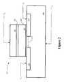
- FIG. 2shows a block diagram illustrating an exemplary flash memory cell, in accordance with one embodiment of the present invention
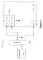
- FIGS. 3A-Bshow block diagrams of exemplary arrangements of a plurality of memory blocks formed on a substrate, in accordance with one embodiment of the present invention
- FIG. 4shows a block diagram of an exemplary arrangement of memory blocks formed in a p-tub, in accordance with one embodiment of the present invention
- FIG. 5shows a block diagram of a circuit that may be used to provide voltages to the p-tub and the memory blocks shown in FIG. 4 , in accordance with one embodiment of the present invention.
- FIG. 6shows a block diagram of a bias circuit that may be used to select memory blocks shown in FIG. 5 , in accordance with one embodiment of the present invention.
- the flash memory array 100includes a plurality of memory blocks 110 , each including a plurality of flash memory cells 115 .
- a 128-Megabit flash memory array 100may include 256 memory blocks 110 , each including 500K flash memory cells 115 .
- Each flash memory cell 115may be coupled to a row line 120 and a column line 125 .
- One or more selected flash memory cells 115may be accessed by providing address signals to a row decoder 130 and a column decoder 135 .
- circuitry in the row decoder 130 and the column decoder 135may select one or more row lines 120 and one or more column lines 125 , which may correspond to the selected flash memory cells 115 .
- the column decoder 135may be coupled to one or more sense amplifiers 140 , which may read the logical state of the selected flash memory cells 115 .
- the selection of flash memory cells 115 through the decoding of row and column addresses, as well as sensing the logical state of flash memory cells 115are well known to those of ordinary skill in the art.
- the flash memory cells 115 in each memory block 110may also be coupled to a bias circuit 160 .
- the row decoder 130 and the column decoder 135may be used to select one or more memory blocks 110 .
- the bias circuit 160may then apply a voltage differential to the one or more selected memory blocks 110 , substantially erasing the flash memory cells 115 in the selected memory blocks 110 .
- the bias circuit 160may apply a voltage differential of 18 volts to substantially erase the selected memory blocks 110 .
- the flash memory cell 115may include a source 210 and a drain 215 that may be formed in a substrate 200 , which may be formed of a variety of semiconductor materials.
- the substrate 200may be an N-type semiconductor formed from silicon.
- a first insulating layer 220may be formed above the source 210 , the drain 215 , and the channel 217 .
- a floating gate 225may be formed above the first insulating layer 220 and a second insulating layer 230 may be formed above the floating gate 225 .
- a control gate 235may then be formed above the first and second insulating layers 220 , 230 .
- a first voltage V 1may be provided to the control gate 235 .
- a second voltage V 2which may be smaller than the first voltage V 1 , may be provided to the drain 215 .
- a third and a fourth voltage V 3 , V 4which may be smaller than the second voltage V 2 , may be provided to the source 210 and the substrate 200 , respectively.
- a first voltage V 1 of about 8 voltsmay be provided to the control gate 235
- a second voltage V 2 of about 4 voltsmay be provided to the drain 215
- a third voltage V 3 of about 0 voltsmay be provided to the source 210
- a fourth voltage V 4 of about 0 voltsmay be provided to the substrate 200 .
- the voltage of about 8 volts on the control gate 235 and the voltage differential of about 4 volts between the source 210 and the drain 215will cause a current of electrons to flow through the channel 217 from the source 210 to the drain 215 .
- the voltage differential of about 8 volts between the control gate 235 and the substrate 200will cause a portion of the electrons to jump from the channel 217 to the floating gate 225 .
- the collected electrons in the floating gate 225may be detected in a reading operation well known to those of ordinary skill in the art and determined to represent a logic-low state.
- the first voltage V 1may be provided to the control gate 235 .
- the third and fourth voltages V 3 , V 4which may be larger than the first voltage V 1 , may be provided to the source 210 and the substrate 200 , respectively.
- the first voltage V 1 of about ⁇ 9 voltsmay be provided to the control gate 235
- the third voltage V 3 of about +9 voltsmay be provided to the source 210
- a fourth voltage V 4 of about +9 voltsmay be provided to the substrate 200 .
- the voltage differential of about 18 volts between the control gate 235 and the substrate 200may cause electrons in the floating gate 225 to jump to the substrate 200 , thus discharging the floating gate 225 .
- the second voltage V 2may be allowed to float.
- FIG. 3Ashows a block diagram of a plurality of memory blocks.
- the first memory block 310 and the second memory block 315may be formed on a substrate 200 .
- the plurality of flash memory cells 115 in the first memory block 310may be erased at substantially the same time using the lines 305 ( 1 - 5 ) that may be coupled to the bias circuit 160 .
- the first and third voltagemay be provided to the plurality of flash memory cells 115 and the substrate 200 at substantially the same time such that the plurality of flash memory cells 115 in the first memory block 310 may be erased at substantially the same time.
- the plurality of flash memory cells 115 in the second memory block 315may be erased at substantially the same time using the lines 306 ( 1 - 5 ) that may be coupled to the bias circuit 160 .
- the voltage differential that may be provided to the flash memory cells 115 in the first memory block 310may erase or have other undesirable effects on at least some of the flash memory cells 115 in other memory blocks. For example, providing the first voltage V 1 of about ⁇ 9 volts to the first memory block 310 and the third voltage V 3 of about +9 volts to the substrate 200 may erase one or more flash memory cells 115 in the second memory block 315 .
- the voltage differentialmay also affect other electronic components, such as logic gates, diodes, and the like, that may be formed in the substrate 200 .
- the first and second memory blocks 310 , 315may be formed in separate p-tubs 320 ( 1 - 2 ).
- the p-tubs 320 ( 1 - 2 )may be P-type regions.
- the p-tubs 320 ( 1 - 2 )may, in one embodiment, be formed in a common n-well 330 , which may be an N-type region formed in the substrate 200 .
- the p-tubsmay each be formed in a separate n-well 340 ( 1 - 2 ).
- the likelihood that the voltage differential provided to the first memory block 310 in the p-tub 320 ( 1 ) will undesirably affect flash memory cells 115 or other components in the p-tub 320 ( 2 )may be reduced.
- providing the first voltage V 1 of about ⁇ 9 volts to the first memory block 310 via the line 305 ( 1 ) and the fourth voltage V 4 of about +9 volts to the p-tub 320 ( 1 ) via the line 305 ( 4 )may substantially erase the plurality of flash memory cells 115 in the first memory block 310 , while leaving the plurality of flash memory cells 115 in the second memory block 315 substantially undisturbed.
- the separation distance 300may be undesirably large and may reduce the number of memory blocks 310 , 315 and other semiconductor components that may be formed on a substrate 200 .
- a 500K memory block 310 , 315may have dimensions of about 80 microns by about 2300 microns, and a desirable separation distance 300 between p-tubs 320 ( 1 ) and 320 ( 2 ) may be about 6 microns.
- a plurality of memory blocks 310 , 315may be placed in one p-tub 320 ( 1 ).
- 70 memory blocks 310 , 315may be placed in the p-tub 320 ( 1 ) with substantially no separation distance 330 between the memory blocks 310 , 315 .
- the voltage differential that may be provided to the flash memory cells 115 in the first memory block 310may erase or have other undesirable effects on the flash memory cells 115 in the second memory block 315 .
- a compensating voltage differentialmay be applied to one or more unselected memory blocks 310 , 315 .
- FIG. 4shows a block diagram of an exemplary arrangement of memory blocks 310 , 315 formed in a p-tub 400 , in accordance with one embodiment of the present invention.
- the bias circuit 160may program the flash memory cells 115 by providing a plurality of voltages to the flash memory cells 115 and the substrate 200 via the lines 305 ( 1 - 5 ), 306 ( 1 - 5 ).
- the bias circuit 160may also provide the plurality of voltages to the lines 305 ( 1 - 5 ) to erase all of the plurality of flash memory cells 115 in the first memory block 310 at substantially the same time.
- the bias circuit 160may also provide the plurality of voltages to the lines 306 ( 1 - 5 ) to erase all of the plurality of flash memory cells 115 in the second memory block 315 at substantially the same time.
- the bias circuit 160may provide a compensating voltage differential to the flash memory cells 115 in the second memory block 315 , in accordance with one embodiment of the present invention.
- the bias circuit 160may provide a voltage of ⁇ 9 volts to the flash memory cells 115 via the line 305 ( 1 ) and a voltage of +9 volts to the p-tub 400 via the lines 305 ( 4 ) and 306 ( 4 ), as well as a voltage of +9 volts to the n-well 330 via the lines 305 ( 5 ), 306 ( 5 ), to erase the first memory block 310 .
- the voltage differential between the control gates 235 of the flash memory cells 115 in the second memory block 315 and the p-tub 400may be reduced to about zero.
- memory blocks 310 , 315are depicted in FIG. 4 , the present invention is not so limited. In alternative embodiments, more memory blocks 310 , 315 may be formed in the p-tub 400 without departing from the scope of the present invention. In one embodiment, for example, 70 memory blocks 310 , 315 each including 500K flash memory cells 115 may be formed in the p-tub 400 .
- FIG. 5shows a block diagram of a circuit 500 that may be used to provide voltages to the p-tub 400 , in accordance with one embodiment of the present invention.
- a controller 510may be coupled to the bias circuit 160 and may select one or more memory blocks 520 ( 1 -n) in the p-tub 400 .
- the bias circuit 160may then provide voltage differentials to erase the selected memory blocks 520 ( 1 -n), as described above.
- the bias circuit 160may provide the compensating voltage differential to the unselected memory blocks 520 ( 1 -n) to reduce the likelihood that the voltage differential provided to the selected memory blocks 520 ( 1 -n) may erase or have other undesirable effects on the unselected memory blocks 520 ( 1 -n).
- the controller 510may select the memory block 520 ( 1 ).
- the bias circuit 160may provide the appropriate erasing voltage differential to the memory block 520 ( 1 ) and may provide the appropriate compensating voltage differential to the unselected memory blocks 520 ( 2 -n).
- every memory block 520 ( 1 -n) of flash memory cells 115 in the p-tub 400will receive biasing voltages, either erasing bias voltages or compensating bias voltages.
- well-known techniques for selecting a memory block 520 ( 1 -n) of flash memory cells 115may be used for applying the erasing biasing voltages, and all memory blocks 520 ( 1 -n), unless selected, would receive compensating biasing voltages.
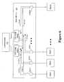
- FIG. 6shows a block diagram of the bias circuit 160 that may be used to select one or more memory blocks 520 ( 1 - 64 ), in accordance with one embodiment of the present invention.
- the bias circuit 160may include one or more decoders 610 ( 1 - 2 ) coupled to a plurality of logic gates 620 ( 1 - 64 ) via one or more lines 613 ( 1 - 8 ), 616 ( 1 - 8 ).
- the logic gates 620 ( 1 - 64 )may be coupled to the memory blocks 520 ( 1 - 64 ).
- the logic gates 620 ( 1 - 64 )may be AND gates.
- FIG. 1shows a block diagram of the bias circuit 160 that may be used to select one or more memory blocks 520 ( 1 - 64 ), in accordance with one embodiment of the present invention.
- the bias circuit 160may include one or more decoders 610 ( 1 - 2 ) coupled to a plurality of logic gates 620 ( 1 - 64 ) via one or more lines 613 (
- FIG. 6shows two decoders 610 ( 1 - 2 ), 64 logic gates 620 ( 1 - 64 ), 16 lines 613 ( 1 - 8 ), 616 ( 1 - 8 ), and 64 memory blocks 520 ( 1 - 64 ).
- the present inventionis not so limited.
- more or fewer decoders 610 ( 1 - 2 ), lines 613 ( 1 - 8 ), 616 ( 1 - 8 ), logic gates 620 ( 1 - 64 ), and memory blocks 520 ( 1 - 64 )may be deployed without departing from the scope of the present invention. Additional desirable elements may also be included in the bias circuit 160 without departing from the scope of the present invention.
- the controller 510may provide a signal to the decoders 610 ( 1 - 2 ), in accordance with one embodiment of the present invention.
- the controller 510may provide a first signal representing a “1” to the decoder 610 ( 1 ) and a second signal representing a “1” to the decoder 610 ( 2 ).
- the decoders 610 ( 1 - 2 )may decode the first and second signals and may then assert a logic-high signal to the lines 613 ( 1 ) and 616 ( 1 ), respectively.
- the decoders 610 ( 1 - 2 )may also assert a logic-low signal to the lines 613 ( 2 - 8 ) and 616 ( 2 - 8 ), respectively.
- the logic gate 620 ( 1 )may use the signals provided by the lines 613 ( 1 ) and 616 ( 1 ) to assert a logic-high signal to the memory block 520 ( 1 ), which may use the asserted signal to provide an erasing voltage to the memory block 520 ( 1 ).
- the unselected logic gates 620 ( 2 - 64 )may assert a logic-low signal that may be used to apply a compensating voltage to the unselected memory blocks 520 ( 2 - 64 ).
Landscapes
- Read Only Memory (AREA)
- Non-Volatile Memory (AREA)
- Semiconductor Memories (AREA)
Abstract
Description
Claims (55)
Priority Applications (2)
| Application Number | Priority Date | Filing Date | Title |
|---|---|---|---|
| US10/228,597US6842380B2 (en) | 2002-08-27 | 2002-08-27 | Method and apparatus for erasing memory |
| US11/003,502US7366027B2 (en) | 2002-08-27 | 2004-12-03 | Method and apparatus for erasing memory |
Applications Claiming Priority (1)
| Application Number | Priority Date | Filing Date | Title |
|---|---|---|---|
| US10/228,597US6842380B2 (en) | 2002-08-27 | 2002-08-27 | Method and apparatus for erasing memory |
Related Child Applications (1)
| Application Number | Title | Priority Date | Filing Date |
|---|---|---|---|
| US11/003,502ContinuationUS7366027B2 (en) | 2002-08-27 | 2004-12-03 | Method and apparatus for erasing memory |
Publications (2)
| Publication Number | Publication Date |
|---|---|
| US20040042271A1 US20040042271A1 (en) | 2004-03-04 |
| US6842380B2true US6842380B2 (en) | 2005-01-11 |
Family
ID=31976066
Family Applications (2)
| Application Number | Title | Priority Date | Filing Date |
|---|---|---|---|
| US10/228,597Expired - LifetimeUS6842380B2 (en) | 2002-08-27 | 2002-08-27 | Method and apparatus for erasing memory |
| US11/003,502Active2026-05-14US7366027B2 (en) | 2002-08-27 | 2004-12-03 | Method and apparatus for erasing memory |
Family Applications After (1)
| Application Number | Title | Priority Date | Filing Date |
|---|---|---|---|
| US11/003,502Active2026-05-14US7366027B2 (en) | 2002-08-27 | 2004-12-03 | Method and apparatus for erasing memory |
Country Status (1)
| Country | Link |
|---|---|
| US (2) | US6842380B2 (en) |
Cited By (9)
| Publication number | Priority date | Publication date | Assignee | Title |
|---|---|---|---|---|
| US20060140012A1 (en)* | 2004-12-29 | 2006-06-29 | Jun Wan | Word line compensation in non-volatile memory erase operations |
| US20060221660A1 (en)* | 2005-03-31 | 2006-10-05 | Hemink Gerrit J | Erasing non-volatile memory using individual verification and additional erasing of subsets of memory cells |
| US20070189081A1 (en)* | 2002-08-27 | 2007-08-16 | Micron Technology, Inc. | Method and apparatus for erasing memory |
| US20080013360A1 (en)* | 2005-03-31 | 2008-01-17 | Hemink Gerrit J | Erase Voltage Manipulation in Non-Volatile Memory for Controlled Shifts in Threshold Voltage |
| US20080019164A1 (en)* | 2005-03-31 | 2008-01-24 | Hemink Gerrit J | Systems for Erase Voltage Manipulation in Non-Volatile Memory for Controlled Shifts in Threshold Voltage |
| US20080089134A1 (en)* | 2006-10-13 | 2008-04-17 | Fumitoshi Ito | Partitioned erase and erase verification in non-volatile memory |
| US20080089135A1 (en)* | 2006-10-13 | 2008-04-17 | Fumitoshi Ito | Systems for partitioned erase and erase verification in non-volatile memory |
| US20080089132A1 (en)* | 2006-10-13 | 2008-04-17 | Fumitoshi Ito | Partitioned soft programming in non-volatile memory |
| US20080089133A1 (en)* | 2006-10-13 | 2008-04-17 | Fumitoshi Ito | Systems for partitioned soft programming in non-volatile memory |
Families Citing this family (1)
| Publication number | Priority date | Publication date | Assignee | Title |
|---|---|---|---|---|
| CN103839586B (en)* | 2014-03-17 | 2017-04-05 | 上海华虹宏力半导体制造有限公司 | The method of adjustment of nonvolatile memory erasing voltage |
Citations (10)
| Publication number | Priority date | Publication date | Assignee | Title |
|---|---|---|---|---|
| US5084843A (en)* | 1987-03-16 | 1992-01-28 | Hitachi, Ltd. | Semiconductor memory having control means for preventing unauthorized erasure of a memory array portion |
| US5323351A (en)* | 1992-06-10 | 1994-06-21 | Nexcom Technology, Inc. | Method and apparatus for programming electrical erasable programmable read-only memory arrays |
| US5926418A (en)* | 1997-04-11 | 1999-07-20 | Programmable Silicon Solutions | Nonvolatile memory |
| US5940324A (en)* | 1997-02-07 | 1999-08-17 | National Semiconductor Corporation | Single-poly EEPROM cell that is programmable and erasable in a low-voltage environment |
| US6344999B1 (en) | 1993-08-27 | 2002-02-05 | Kabushiki Kaisha Toshiba | Non-volatile semiconductor memory device and data programming method |
| US6344995B2 (en) | 1998-12-02 | 2002-02-05 | Winbond Electronics Corp. | Circuit for controlling the potential difference between the substrate and the control gate on non-volatile memory and its control method |
| US6344996B2 (en) | 1997-04-07 | 2002-02-05 | Kabushiki Kaisha Toshiba | Semiconductor memory device |
| US6345000B1 (en) | 1997-04-16 | 2002-02-05 | Sandisk Corporation | Flash memory permitting simultaneous read/write and erase operations in a single memory array |
| US6345367B1 (en) | 1996-07-11 | 2002-02-05 | Memory Corporation Plc | Defective memory block handling system by addressing a group of memory blocks for erasure and changing the content therewith |
| US6487120B2 (en)* | 2000-05-25 | 2002-11-26 | Kabushiki Kaisha Toshiba | Boosted voltage generating circuit and semiconductor memory device having the same |
Family Cites Families (2)
| Publication number | Priority date | Publication date | Assignee | Title |
|---|---|---|---|---|
| JP3789241B2 (en)* | 1998-12-01 | 2006-06-21 | Necエレクトロニクス株式会社 | Bias circuit and semiconductor memory device |
| US6842380B2 (en)* | 2002-08-27 | 2005-01-11 | Micron Technology, Inc. | Method and apparatus for erasing memory |
- 2002
- 2002-08-27USUS10/228,597patent/US6842380B2/ennot_activeExpired - Lifetime
- 2004
- 2004-12-03USUS11/003,502patent/US7366027B2/enactiveActive
Patent Citations (10)
| Publication number | Priority date | Publication date | Assignee | Title |
|---|---|---|---|---|
| US5084843A (en)* | 1987-03-16 | 1992-01-28 | Hitachi, Ltd. | Semiconductor memory having control means for preventing unauthorized erasure of a memory array portion |
| US5323351A (en)* | 1992-06-10 | 1994-06-21 | Nexcom Technology, Inc. | Method and apparatus for programming electrical erasable programmable read-only memory arrays |
| US6344999B1 (en) | 1993-08-27 | 2002-02-05 | Kabushiki Kaisha Toshiba | Non-volatile semiconductor memory device and data programming method |
| US6345367B1 (en) | 1996-07-11 | 2002-02-05 | Memory Corporation Plc | Defective memory block handling system by addressing a group of memory blocks for erasure and changing the content therewith |
| US5940324A (en)* | 1997-02-07 | 1999-08-17 | National Semiconductor Corporation | Single-poly EEPROM cell that is programmable and erasable in a low-voltage environment |
| US6344996B2 (en) | 1997-04-07 | 2002-02-05 | Kabushiki Kaisha Toshiba | Semiconductor memory device |
| US5926418A (en)* | 1997-04-11 | 1999-07-20 | Programmable Silicon Solutions | Nonvolatile memory |
| US6345000B1 (en) | 1997-04-16 | 2002-02-05 | Sandisk Corporation | Flash memory permitting simultaneous read/write and erase operations in a single memory array |
| US6344995B2 (en) | 1998-12-02 | 2002-02-05 | Winbond Electronics Corp. | Circuit for controlling the potential difference between the substrate and the control gate on non-volatile memory and its control method |
| US6487120B2 (en)* | 2000-05-25 | 2002-11-26 | Kabushiki Kaisha Toshiba | Boosted voltage generating circuit and semiconductor memory device having the same |
Cited By (33)
| Publication number | Priority date | Publication date | Assignee | Title |
|---|---|---|---|---|
| US20070189081A1 (en)* | 2002-08-27 | 2007-08-16 | Micron Technology, Inc. | Method and apparatus for erasing memory |
| US7366027B2 (en)* | 2002-08-27 | 2008-04-29 | Micron Technology, Inc. | Method and apparatus for erasing memory |
| US7606074B2 (en) | 2004-12-29 | 2009-10-20 | Sandisk Corporation | Word line compensation in non-volatile memory erase operations |
| US20090021983A1 (en)* | 2004-12-29 | 2009-01-22 | Sandisk Corporation | Word Line Compensation In Non-Volatile Memory Erase Operations |
| US7450433B2 (en)* | 2004-12-29 | 2008-11-11 | Sandisk Corporation | Word line compensation in non-volatile memory erase operations |
| US20060140012A1 (en)* | 2004-12-29 | 2006-06-29 | Jun Wan | Word line compensation in non-volatile memory erase operations |
| US7403424B2 (en) | 2005-03-31 | 2008-07-22 | Sandisk Corporation | Erasing non-volatile memory using individual verification and additional erasing of subsets of memory cells |
| US7400537B2 (en) | 2005-03-31 | 2008-07-15 | Sandisk Corporation | Systems for erasing non-volatile memory using individual verification and additional erasing of subsets of memory cells |
| US20080013360A1 (en)* | 2005-03-31 | 2008-01-17 | Hemink Gerrit J | Erase Voltage Manipulation in Non-Volatile Memory for Controlled Shifts in Threshold Voltage |
| US20080019164A1 (en)* | 2005-03-31 | 2008-01-24 | Hemink Gerrit J | Systems for Erase Voltage Manipulation in Non-Volatile Memory for Controlled Shifts in Threshold Voltage |
| US20060221660A1 (en)* | 2005-03-31 | 2006-10-05 | Hemink Gerrit J | Erasing non-volatile memory using individual verification and additional erasing of subsets of memory cells |
| US7606100B2 (en) | 2005-03-31 | 2009-10-20 | Sandisk Corporation | Erasing non-volatile memory using individual verification and additional erasing of subsets of memory cells |
| US7522457B2 (en) | 2005-03-31 | 2009-04-21 | Sandisk Corporation | Systems for erase voltage manipulation in non-volatile memory for controlled shifts in threshold voltage |
| US20060221708A1 (en)* | 2005-03-31 | 2006-10-05 | Masaaki Higashitani | Erasing non-volatile memory utilizing changing word line conditions to compensate for slower erasing memory cells |
| US20060221703A1 (en)* | 2005-03-31 | 2006-10-05 | Masaaki Higashitani | Systems for erasing non-volatile memory utilizing changing word line conditions to compensate for slower erasing memory cells |
| US7486564B2 (en) | 2005-03-31 | 2009-02-03 | Sandisk Corporation | Soft programming non-volatile memory utilizing individual verification and additional soft programming of subsets of memory cells |
| US20060221705A1 (en)* | 2005-03-31 | 2006-10-05 | Hemink Gerrit J | Soft programming non-volatile memory utilizing individual verification and additional soft programming of subsets of memory cells |
| US7403428B2 (en) | 2005-03-31 | 2008-07-22 | Sandisk Corporation | Systems for erasing non-volatile memory utilizing changing word line conditions to compensate for slower erasing memory cells |
| US7408804B2 (en) | 2005-03-31 | 2008-08-05 | Sandisk Corporation | Systems for soft programming non-volatile memory utilizing individual verification and additional soft programming of subsets of memory cells |
| US7430138B2 (en) | 2005-03-31 | 2008-09-30 | Sandisk Corporation | Erasing non-volatile memory utilizing changing word line conditions to compensate for slower erasing memory cells |
| US20060221709A1 (en)* | 2005-03-31 | 2006-10-05 | Hemink Gerrit J | Systems for erasing non-volatile memory using individual verification and additional erasing of subsets of memory cells |
| US7457166B2 (en) | 2005-03-31 | 2008-11-25 | Sandisk Corporation | Erase voltage manipulation in non-volatile memory for controlled shifts in threshold voltage |
| US20060221661A1 (en)* | 2005-03-31 | 2006-10-05 | Hemink Gerrit J | Systems for soft programming non-volatile memory utilizing individual verification and additional soft programming of subsets of memory cells |
| US20080089133A1 (en)* | 2006-10-13 | 2008-04-17 | Fumitoshi Ito | Systems for partitioned soft programming in non-volatile memory |
| US7495954B2 (en) | 2006-10-13 | 2009-02-24 | Sandisk Corporation | Method for partitioned erase and erase verification to compensate for capacitive coupling effects in non-volatile memory |
| US7499317B2 (en) | 2006-10-13 | 2009-03-03 | Sandisk Corporation | System for partitioned erase and erase verification in a non-volatile memory to compensate for capacitive coupling |
| US7499338B2 (en) | 2006-10-13 | 2009-03-03 | Sandisk Corporation | Partitioned soft programming in non-volatile memory |
| US20080089132A1 (en)* | 2006-10-13 | 2008-04-17 | Fumitoshi Ito | Partitioned soft programming in non-volatile memory |
| US7535766B2 (en) | 2006-10-13 | 2009-05-19 | Sandisk Corporation | Systems for partitioned soft programming in non-volatile memory |
| US20090180325A1 (en)* | 2006-10-13 | 2009-07-16 | Sandisk Corporation | Partitioned Erase And Erase Verification In Non-Volatile Memory |
| US20080089135A1 (en)* | 2006-10-13 | 2008-04-17 | Fumitoshi Ito | Systems for partitioned erase and erase verification in non-volatile memory |
| US20080089134A1 (en)* | 2006-10-13 | 2008-04-17 | Fumitoshi Ito | Partitioned erase and erase verification in non-volatile memory |
| US7768826B2 (en) | 2006-10-13 | 2010-08-03 | Sandisk Corporation | Methods for partitioned erase and erase verification in non-volatile memory to compensate for capacitive coupling effects |
Also Published As
| Publication number | Publication date |
|---|---|
| US7366027B2 (en) | 2008-04-29 |
| US20070189081A1 (en) | 2007-08-16 |
| US20040042271A1 (en) | 2004-03-04 |
Similar Documents
| Publication | Publication Date | Title |
|---|---|---|
| US6657894B2 (en) | Apparatus and method for programming virtual ground nonvolatile memory cell array without disturbing adjacent cells | |
| US6545910B2 (en) | Non-volatile semiconductor memory device having word line defect check circuit | |
| US5465231A (en) | EEPROM and logic LSI chip including such EEPROM | |
| US6525969B1 (en) | Decoder apparatus and methods for pre-charging bit lines | |
| KR920001917B1 (en) | Nonvolatile Semiconductor Memory | |
| US6510082B1 (en) | Drain side sensing scheme for virtual ground flash EPROM array with adjacent bit charge and hold | |
| US6380636B1 (en) | Nonvolatile semiconductor memory device having an array structure suitable to high-density integrationization | |
| JP4504405B2 (en) | Semiconductor memory device | |
| JP2005510889A (en) | Semiconductor device having EEPROM erasable EEPROM memory | |
| US7710759B2 (en) | Nonvolatile ferroelectric memory device | |
| US5392238A (en) | Nonvolatile semiconductor memory device | |
| US5706228A (en) | Method for operating a memory array | |
| KR960005896B1 (en) | Semiconductor memory | |
| US6798694B2 (en) | Method for reducing drain disturb in programming | |
| JPH1145986A (en) | Non-volatile semiconductor storage device | |
| US6842380B2 (en) | Method and apparatus for erasing memory | |
| US7095653B2 (en) | Common wordline flash array architecture | |
| JPH06291332A (en) | Semiconductor memory device and method of using the same | |
| US9947620B2 (en) | Semiconductor memory device | |
| KR0145164B1 (en) | Word line redundant nonvolatile semiconductor memory | |
| US7352605B2 (en) | Nonvolatile ferroelectric memory device and method thereof | |
| US7583538B2 (en) | Semiconductor memory and read method of the same | |
| US8508993B2 (en) | Method and apparatus of performing an erase operation on a memory integrated circuit | |
| US20090116289A1 (en) | Decoding system capable of reducing sector select area overhead for flash memory | |
| JP2007294109A (en) | Memory element and data read-out method |
Legal Events
| Date | Code | Title | Description |
|---|---|---|---|
| AS | Assignment | Owner name:MICRON TECHNOLOGY, INC., IDAHO Free format text:ASSIGNMENT OF ASSIGNORS INTEREST;ASSIGNORS:LAKHANI, VINOD;LIU, TZ-YI;REEL/FRAME:013422/0131 Effective date:20021007 | |
| STCF | Information on status: patent grant | Free format text:PATENTED CASE | |
| FPAY | Fee payment | Year of fee payment:4 | |
| FPAY | Fee payment | Year of fee payment:8 | |
| AS | Assignment | Owner name:U.S. BANK NATIONAL ASSOCIATION, AS COLLATERAL AGENT, CALIFORNIA Free format text:SECURITY INTEREST;ASSIGNOR:MICRON TECHNOLOGY, INC.;REEL/FRAME:038669/0001 Effective date:20160426 Owner name:U.S. BANK NATIONAL ASSOCIATION, AS COLLATERAL AGEN Free format text:SECURITY INTEREST;ASSIGNOR:MICRON TECHNOLOGY, INC.;REEL/FRAME:038669/0001 Effective date:20160426 | |
| AS | Assignment | Owner name:MORGAN STANLEY SENIOR FUNDING, INC., AS COLLATERAL AGENT, MARYLAND Free format text:PATENT SECURITY AGREEMENT;ASSIGNOR:MICRON TECHNOLOGY, INC.;REEL/FRAME:038954/0001 Effective date:20160426 Owner name:MORGAN STANLEY SENIOR FUNDING, INC., AS COLLATERAL Free format text:PATENT SECURITY AGREEMENT;ASSIGNOR:MICRON TECHNOLOGY, INC.;REEL/FRAME:038954/0001 Effective date:20160426 | |
| FPAY | Fee payment | Year of fee payment:12 | |
| AS | Assignment | Owner name:U.S. BANK NATIONAL ASSOCIATION, AS COLLATERAL AGENT, CALIFORNIA Free format text:CORRECTIVE ASSIGNMENT TO CORRECT THE REPLACE ERRONEOUSLY FILED PATENT #7358718 WITH THE CORRECT PATENT #7358178 PREVIOUSLY RECORDED ON REEL 038669 FRAME 0001. ASSIGNOR(S) HEREBY CONFIRMS THE SECURITY INTEREST;ASSIGNOR:MICRON TECHNOLOGY, INC.;REEL/FRAME:043079/0001 Effective date:20160426 Owner name:U.S. BANK NATIONAL ASSOCIATION, AS COLLATERAL AGEN Free format text:CORRECTIVE ASSIGNMENT TO CORRECT THE REPLACE ERRONEOUSLY FILED PATENT #7358718 WITH THE CORRECT PATENT #7358178 PREVIOUSLY RECORDED ON REEL 038669 FRAME 0001. ASSIGNOR(S) HEREBY CONFIRMS THE SECURITY INTEREST;ASSIGNOR:MICRON TECHNOLOGY, INC.;REEL/FRAME:043079/0001 Effective date:20160426 | |
| AS | Assignment | Owner name:JPMORGAN CHASE BANK, N.A., AS COLLATERAL AGENT, ILLINOIS Free format text:SECURITY INTEREST;ASSIGNORS:MICRON TECHNOLOGY, INC.;MICRON SEMICONDUCTOR PRODUCTS, INC.;REEL/FRAME:047540/0001 Effective date:20180703 Owner name:JPMORGAN CHASE BANK, N.A., AS COLLATERAL AGENT, IL Free format text:SECURITY INTEREST;ASSIGNORS:MICRON TECHNOLOGY, INC.;MICRON SEMICONDUCTOR PRODUCTS, INC.;REEL/FRAME:047540/0001 Effective date:20180703 | |
| AS | Assignment | Owner name:MICRON TECHNOLOGY, INC., IDAHO Free format text:RELEASE BY SECURED PARTY;ASSIGNOR:U.S. BANK NATIONAL ASSOCIATION, AS COLLATERAL AGENT;REEL/FRAME:047243/0001 Effective date:20180629 | |
| AS | Assignment | Owner name:MICRON TECHNOLOGY, INC., IDAHO Free format text:RELEASE BY SECURED PARTY;ASSIGNOR:MORGAN STANLEY SENIOR FUNDING, INC., AS COLLATERAL AGENT;REEL/FRAME:050937/0001 Effective date:20190731 | |
| AS | Assignment | Owner name:MICRON SEMICONDUCTOR PRODUCTS, INC., IDAHO Free format text:RELEASE BY SECURED PARTY;ASSIGNOR:JPMORGAN CHASE BANK, N.A., AS COLLATERAL AGENT;REEL/FRAME:051028/0001 Effective date:20190731 Owner name:MICRON TECHNOLOGY, INC., IDAHO Free format text:RELEASE BY SECURED PARTY;ASSIGNOR:JPMORGAN CHASE BANK, N.A., AS COLLATERAL AGENT;REEL/FRAME:051028/0001 Effective date:20190731 |