US6842170B1 - Display with aligned optical shutter and backlight cells applicable for use with a touchscreen - Google Patents
Display with aligned optical shutter and backlight cells applicable for use with a touchscreenDownload PDFInfo
- Publication number
- US6842170B1 US6842170B1US09/271,634US27163499AUS6842170B1US 6842170 B1US6842170 B1US 6842170B1US 27163499 AUS27163499 AUS 27163499AUS 6842170 B1US6842170 B1US 6842170B1
- Authority
- US
- United States
- Prior art keywords
- layer
- backlight
- pixels
- optical shutter
- display
- Prior art date
- Legal status (The legal status is an assumption and is not a legal conclusion. Google has not performed a legal analysis and makes no representation as to the accuracy of the status listed.)
- Expired - Fee Related
Links
Images


Classifications
- G—PHYSICS
- G06—COMPUTING OR CALCULATING; COUNTING
- G06F—ELECTRIC DIGITAL DATA PROCESSING
- G06F3/00—Input arrangements for transferring data to be processed into a form capable of being handled by the computer; Output arrangements for transferring data from processing unit to output unit, e.g. interface arrangements
- G06F3/01—Input arrangements or combined input and output arrangements for interaction between user and computer
- G06F3/03—Arrangements for converting the position or the displacement of a member into a coded form
- G06F3/033—Pointing devices displaced or positioned by the user, e.g. mice, trackballs, pens or joysticks; Accessories therefor
- G06F3/0354—Pointing devices displaced or positioned by the user, e.g. mice, trackballs, pens or joysticks; Accessories therefor with detection of 2D relative movements between the device, or an operating part thereof, and a plane or surface, e.g. 2D mice, trackballs, pens or pucks
- G06F3/03547—Touch pads, in which fingers can move on a surface
- E—FIXED CONSTRUCTIONS
- E05—LOCKS; KEYS; WINDOW OR DOOR FITTINGS; SAFES
- E05B—LOCKS; ACCESSORIES THEREFOR; HANDCUFFS
- E05B1/00—Knobs or handles for wings; Knobs, handles, or press buttons for locks or latches on wings
- E05B1/04—Knobs or handles for wings; Knobs, handles, or press buttons for locks or latches on wings with inner rigid member and outer cover or covers
- B—PERFORMING OPERATIONS; TRANSPORTING
- B05—SPRAYING OR ATOMISING IN GENERAL; APPLYING FLUENT MATERIALS TO SURFACES, IN GENERAL
- B05D—PROCESSES FOR APPLYING FLUENT MATERIALS TO SURFACES, IN GENERAL
- B05D5/00—Processes for applying liquids or other fluent materials to surfaces to obtain special surface effects, finishes or structures
- B05D5/06—Processes for applying liquids or other fluent materials to surfaces to obtain special surface effects, finishes or structures to obtain multicolour or other optical effects
- G—PHYSICS
- G02—OPTICS
- G02F—OPTICAL DEVICES OR ARRANGEMENTS FOR THE CONTROL OF LIGHT BY MODIFICATION OF THE OPTICAL PROPERTIES OF THE MEDIA OF THE ELEMENTS INVOLVED THEREIN; NON-LINEAR OPTICS; FREQUENCY-CHANGING OF LIGHT; OPTICAL LOGIC ELEMENTS; OPTICAL ANALOGUE/DIGITAL CONVERTERS
- G02F1/00—Devices or arrangements for the control of the intensity, colour, phase, polarisation or direction of light arriving from an independent light source, e.g. switching, gating or modulating; Non-linear optics
- G02F1/01—Devices or arrangements for the control of the intensity, colour, phase, polarisation or direction of light arriving from an independent light source, e.g. switching, gating or modulating; Non-linear optics for the control of the intensity, phase, polarisation or colour
- G02F1/13—Devices or arrangements for the control of the intensity, colour, phase, polarisation or direction of light arriving from an independent light source, e.g. switching, gating or modulating; Non-linear optics for the control of the intensity, phase, polarisation or colour based on liquid crystals, e.g. single liquid crystal display cells
- G02F1/133—Constructional arrangements; Operation of liquid crystal cells; Circuit arrangements
- G02F1/1333—Constructional arrangements; Manufacturing methods
- G02F1/1335—Structural association of cells with optical devices, e.g. polarisers or reflectors
- G02F1/1336—Illuminating devices
- G02F1/133602—Direct backlight
- G02F1/133603—Direct backlight with LEDs
- G—PHYSICS
- G06—COMPUTING OR CALCULATING; COUNTING
- G06F—ELECTRIC DIGITAL DATA PROCESSING
- G06F3/00—Input arrangements for transferring data to be processed into a form capable of being handled by the computer; Output arrangements for transferring data from processing unit to output unit, e.g. interface arrangements
- G06F3/01—Input arrangements or combined input and output arrangements for interaction between user and computer
- G06F3/03—Arrangements for converting the position or the displacement of a member into a coded form
- G06F3/041—Digitisers, e.g. for touch screens or touch pads, characterised by the transducing means
- G06F3/0412—Digitisers structurally integrated in a display
- G—PHYSICS
- G09—EDUCATION; CRYPTOGRAPHY; DISPLAY; ADVERTISING; SEALS
- G09G—ARRANGEMENTS OR CIRCUITS FOR CONTROL OF INDICATING DEVICES USING STATIC MEANS TO PRESENT VARIABLE INFORMATION
- G09G3/00—Control arrangements or circuits, of interest only in connection with visual indicators other than cathode-ray tubes
- G09G3/20—Control arrangements or circuits, of interest only in connection with visual indicators other than cathode-ray tubes for presentation of an assembly of a number of characters, e.g. a page, by composing the assembly by combination of individual elements arranged in a matrix no fixed position being assigned to or needed to be assigned to the individual characters or partial characters
- G09G3/34—Control arrangements or circuits, of interest only in connection with visual indicators other than cathode-ray tubes for presentation of an assembly of a number of characters, e.g. a page, by composing the assembly by combination of individual elements arranged in a matrix no fixed position being assigned to or needed to be assigned to the individual characters or partial characters by control of light from an independent source
- G09G3/3406—Control of illumination source
- G09G3/342—Control of illumination source using several illumination sources separately controlled corresponding to different display panel areas, e.g. along one dimension such as lines
- H—ELECTRICITY
- H04—ELECTRIC COMMUNICATION TECHNIQUE
- H04M—TELEPHONIC COMMUNICATION
- H04M1/00—Substation equipment, e.g. for use by subscribers
- H04M1/02—Constructional features of telephone sets
- H04M1/22—Illumination; Arrangements for improving the visibility of characters on dials
- G—PHYSICS
- G02—OPTICS
- G02F—OPTICAL DEVICES OR ARRANGEMENTS FOR THE CONTROL OF LIGHT BY MODIFICATION OF THE OPTICAL PROPERTIES OF THE MEDIA OF THE ELEMENTS INVOLVED THEREIN; NON-LINEAR OPTICS; FREQUENCY-CHANGING OF LIGHT; OPTICAL LOGIC ELEMENTS; OPTICAL ANALOGUE/DIGITAL CONVERTERS
- G02F1/00—Devices or arrangements for the control of the intensity, colour, phase, polarisation or direction of light arriving from an independent light source, e.g. switching, gating or modulating; Non-linear optics
- G02F1/01—Devices or arrangements for the control of the intensity, colour, phase, polarisation or direction of light arriving from an independent light source, e.g. switching, gating or modulating; Non-linear optics for the control of the intensity, phase, polarisation or colour
- G02F1/13—Devices or arrangements for the control of the intensity, colour, phase, polarisation or direction of light arriving from an independent light source, e.g. switching, gating or modulating; Non-linear optics for the control of the intensity, phase, polarisation or colour based on liquid crystals, e.g. single liquid crystal display cells
- G02F1/133—Constructional arrangements; Operation of liquid crystal cells; Circuit arrangements
- G02F1/1333—Constructional arrangements; Manufacturing methods
- G02F1/13338—Input devices, e.g. touch panels
- G—PHYSICS
- G02—OPTICS
- G02F—OPTICAL DEVICES OR ARRANGEMENTS FOR THE CONTROL OF LIGHT BY MODIFICATION OF THE OPTICAL PROPERTIES OF THE MEDIA OF THE ELEMENTS INVOLVED THEREIN; NON-LINEAR OPTICS; FREQUENCY-CHANGING OF LIGHT; OPTICAL LOGIC ELEMENTS; OPTICAL ANALOGUE/DIGITAL CONVERTERS
- G02F1/00—Devices or arrangements for the control of the intensity, colour, phase, polarisation or direction of light arriving from an independent light source, e.g. switching, gating or modulating; Non-linear optics
- G02F1/01—Devices or arrangements for the control of the intensity, colour, phase, polarisation or direction of light arriving from an independent light source, e.g. switching, gating or modulating; Non-linear optics for the control of the intensity, phase, polarisation or colour
- G02F1/13—Devices or arrangements for the control of the intensity, colour, phase, polarisation or direction of light arriving from an independent light source, e.g. switching, gating or modulating; Non-linear optics for the control of the intensity, phase, polarisation or colour based on liquid crystals, e.g. single liquid crystal display cells
- G02F1/133—Constructional arrangements; Operation of liquid crystal cells; Circuit arrangements
- G02F1/1333—Constructional arrangements; Manufacturing methods
- G02F1/1334—Constructional arrangements; Manufacturing methods based on polymer dispersed liquid crystals, e.g. microencapsulated liquid crystals
- G—PHYSICS
- G02—OPTICS
- G02F—OPTICAL DEVICES OR ARRANGEMENTS FOR THE CONTROL OF LIGHT BY MODIFICATION OF THE OPTICAL PROPERTIES OF THE MEDIA OF THE ELEMENTS INVOLVED THEREIN; NON-LINEAR OPTICS; FREQUENCY-CHANGING OF LIGHT; OPTICAL LOGIC ELEMENTS; OPTICAL ANALOGUE/DIGITAL CONVERTERS
- G02F1/00—Devices or arrangements for the control of the intensity, colour, phase, polarisation or direction of light arriving from an independent light source, e.g. switching, gating or modulating; Non-linear optics
- G02F1/01—Devices or arrangements for the control of the intensity, colour, phase, polarisation or direction of light arriving from an independent light source, e.g. switching, gating or modulating; Non-linear optics for the control of the intensity, phase, polarisation or colour
- G02F1/13—Devices or arrangements for the control of the intensity, colour, phase, polarisation or direction of light arriving from an independent light source, e.g. switching, gating or modulating; Non-linear optics for the control of the intensity, phase, polarisation or colour based on liquid crystals, e.g. single liquid crystal display cells
- G02F1/133—Constructional arrangements; Operation of liquid crystal cells; Circuit arrangements
- G02F1/1333—Constructional arrangements; Manufacturing methods
- G02F1/1335—Structural association of cells with optical devices, e.g. polarisers or reflectors
- G02F1/1336—Illuminating devices
- G02F1/133621—Illuminating devices providing coloured light
Definitions
- This inventionrelates generally to displays, and more particularly to an optical shutter-type display having a light source and applicable for use with a touchscreen.
- a standard emissive displayuses a pixelated, or patterned, light source in which different regions of the display can be selectively turned on to emit light. Regions of the display that are turned off do not emit light; however, in bright light situations, the “off” portion of the display can be as bright or brighter than the “on” portion of the display due to the highly reflective nature of the light-emitting materials (generally phosphors).
- a contrast filteralso called a neutral density filter, can be placed over the display and uses a partially light-absorbing film to absorb some of the emitted and reflected light from the display. The filter, however, reduces the brightness of the display in all viewing conditions.
- Polymer-dispersed liquid crystal (PDLC) display technologyis a low-cost, all-plastic display technology using micron-sized liquid crystal droplets dispersed in a solid polymer matrix.
- Dichroic dye molecules added to the liquid crystal dropletscause a PDLC display to exhibit the color of the dye when no electric field is applied to the display. In this colored state, the dye molecules and liquid crystal droplets are randomly arranged and the display is opaque. This is conceptually a “closed optical shutter” condition. When an electric field of predetermined strength and orientation is applied, the dye molecules and the liquid crystal droplets reorient to allow light to pass through the PDLC layer. This is conceptually an “open optical shutter” condition. In this transparent state, the display reveals the color of the display backing.
- the display backingis a reflective surface
- ambient lightmakes two passes through the PDLC layer where the PDLC is in an open shutter condition.
- Optimizing the display for bright-light environmentsrequires using a PDLC dye molecule concentration where the closed shutter state is dark yet without excess residual absorption in the open shutter state that would affect the display brightness.
- a PDLC displaycan be backlit. When the display is backlit, however, the backlight only makes one pass through the PDLC display.
- the backlit displayhas significantly degraded contrast and the “off” pixels can appear to be turned on.
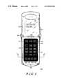
- FIG. 1shows an electronic device implementing a display with aligned optical shutter and backlight cells over a touchscreen according to a preferred embodiment.
- FIG. 2shows a cross section of a display with aligned optical shutter and backlight cells over a touchscreen along line 2 — 2 of FIG. 1 according to a preferred embodiment.
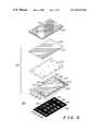
- FIG. 3shows an exploded view of the optical shutter cell side of the display shown in FIG. 2 .
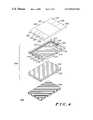
- FIG. 4shows an exploded view of the backlight cell side of the display shown in FIG. 2 .
- FIG. 5shows various alternate embodiments of a display with aligned optical shutter and backlight cells applicable for use with a touchscreen.
- a display with aligned optical shutter and backlight cellsuses a patterned polymer-dispersed liquid crystal (PDLC) optical shutter and a patterned electroluminescent (EL) backlight to provide a low-cost, low-current-drain display having good contrast in both bright-light and low-light conditions.
- the aligned, patterned optical shutter and backlight layersform pixel “windows” through which images printed on a background can be hidden or revealed.
- a black maskbears the images and is inserted between the optical shutter and the backlight layers to show information images, cover inactive areas of the display, and cover electrode traces connecting active segments of the display.
- the display with aligned optical shutter and backlight cellsis thin and flexible enough to be integrated with a touchscreen.
- the displaycan be used to implement a keypad for a portable electronic device, such as a radiotelephone, by exhibiting the numbers and icons common to such user interfaces.
- a portable electronic devicesuch as a radiotelephone
- a usercould dial a telephone number by pressing the appropriate sections of the touchscreen, or enter phonebook information using handwriting recognition, or use the touchscreen for mouse operation.
- a pixelwill refer to the smallest region in an optical shutter or a backlight, or an optical shutter aligned with a backlight, that can be individually controlled to turn on and turn off.
- a pixelcan be controlled using direct drive or matrix addressing.
- a pixelneed not be a contiguous area; it can be disjoint areas that are controlled together (e.g., both the dot and the line in a lower-case “i” can make up a single pixel).
- FIG. 1shows an electronic device 100 implementing a display with aligned optical shutter and backlight cells integrated with a touchscreen according to a preferred embodiment.
- the electronic device 100 shownis a radiotelephone, however, the display with aligned optical shutter and backlight cells can also be implemented in personal digital assistants, television remote controls, video cassette players, household appliances, automobile dashboards, billboards, point-of-sale displays, landline telephones, and other electronic devices.
- the electronic device 100has a first housing 102 and a second housing 104 movably connected by a hinge 106 .
- the first housing 102 and the second housing 104pivot between an open position and a closed position.
- An antenna 101transmits and receives radio frequency signals for communicating with a complementary electronic device such as a cellular base station.
- a display 110 positioned on the first housing 102can be used for functions such as displaying names, telephone numbers, transmitted and received information, user interface commands, scrolled menus, and other information.
- a microphone 118receives sound for transmission, and an audio speaker 116 transmits audio signals to a user.
- a keyless input device 150is carried by the second housing 104 .
- the keyless input device 150is implemented as a touchscreen with a display. In the drawing, multiple images on the display are delineated with dashed lines.
- a main image 151represents a standard, twelve-key telephone keypad.
- images 152 , 153 , 154 , 156represent an on/off button, a function button, a handwriting recognition mode button, and a telephone mode button.
- images 157 , 158 , 159represent a “clear” button, a phonebook mode button, and an “OK” button.
- Each image 151 , 152 , 153 , 154 , 156 , 157 , 158 , 159is a direct driven pixel, and this keyless input device uses a display with aligned optical shutter and backlight cells to selectively reveal one or more images and provide contrast for the revealed images in both low-light and bright-light conditions.
- FIG. 2shows a cross section of a display 200 with aligned optical shutter and backlight cells over a touchscreen along line 2 — 2 of FIG. 1 according to a preferred embodiment.
- the preferred embodimentis a stack with multiple layers including an optical shutter cell 239 , an optional mask layer 250 , an optional color layer 260 , a backlight cell 289 , and an optional touchscreen 290 .
- a user 201sees a top layer 210 , which is an ultra-violet barrier with a matte upper surface 215 to reduce glare.
- the top layer 210is printed directly onto the top substrate 220 of the PDLC optical shutter cell 239 .
- the PDLC optical shutter cell 239is made from a PDLC optical shutter material 230 sandwiched between two electrodes 225 , 245 and two substrates 220 , 240 .
- the electrodes and substratesare preferably transparent.
- the upper electrode 225is preferably constructed using a solid indium-tin oxide (In 2 O 3 —SnO 2 ) (ITO) layer affixed to the substrate 220 adjacent to the PDLC optical shutter material 230 .
- ITOsolid indium-tin oxide
- the lower electrode 245is preferably constructed using a patterned ITO layer affixed to the lower substrate 240 adjacent to the PDLC optical shutter material 230 . If desired, both electrodes 225 , 245 can be patterned; however, the user 201 may see the patterning if it is implemented on the top electrode 225 .
- One electrode 245is connected to an external power supply via an optical shutter cell driver bus 237 to create an electric field of a predetermined strength while the other electrode 225 acts as a ground. The direction of the electric field is not important to the optical shutter, thus either electrode can act as the ground.
- the electric field created by the electrodes 225 , 245alter the light transmission properties of the PDLC optical shutter material 230 , and the pattern of the patterned electrode layer 245 defines pixels of the display. These pixels lay over the images 151 , 152 , 153 , 154 , 156 , 157 , 158 , 159 of the keyless input device shown in FIG. 1 .
- the liquid crystal material and dichroic dye in the PDLC materialare randomly aligned and absorb most incident light.
- the liquid crystal material and dichroic dyealign in the direction of the applied field and transmit substantial amounts of incident light. In this manner, a pixel of the PDLC cell can be switched from a relatively non-transparent state to a relatively transparent state.
- Each pixelcan be independently controlled to be closed-shuttered or open-shuttered, depending on the application of an electric field.
- a mask layer 250bears images that include buttons for the keyless input device 150 shown in FIG. 1 .
- Each buttonis underneath a pixel in the optical shutter cell 239 .
- the pixelsact as “windows” with optical shutters that can be open or closed, to reveal an image 151 , 152 , 153 , 154 , 156 , 157 , 158 , 159 shown in FIG. 1 borne by the mask.
- the patterned area in the patterned electrode 245can be easily aligned with the mask layer 250 .
- the mask layer 250is screen printed directly onto the bottom surface of the lower transparent substrate 240 .
- the mask layer 250is a color layer 260 having one or more colors.
- color transflector blocksare aligned so that each image 151 , 152 , 153 , 154 , 156 , 157 , 158 , 159 shown in FIG. 1 is a single color.
- a transflectorhas both transmission and reflection properties.
- the color layer 260may alternatively be made of color filters, which only have transmission properties.
- a backlight cell 289includes a layer of backlight material 280 sandwiched between a transparent substrate 270 bearing a patterned ITO electrode 275 and a ground electrode 285 .
- the patterned electrode 275 for the backlight cell 289is aligned with and has the same pattern as the patterned electrode 245 for the optical shutter cell 239 .
- the ground electrode 285is a solid conductive ink layer printed directly onto the bottom surface of the backlight material 280 ; however, the ground electrode 285 may be patterned and may be borne on a transparent or non-transparent substrate if desired.
- One electrode layer 275is connected to an external power supply via a backlight cell driver bus 287 to create an electric field of a predetermined strength.
- a backlight cell driver bus 287can act as the ground.
- the voltage response and frequency drive requirements of the optical shutter cell 239are similar to the backlight cell 289 .
- the backlight cell driver bus 287 and the optical shutter cell driver bus 237can be connected to common drive electronics 299 for simultaneous control of pixels in the backlight cell and the optical shutter cell.
- the optical shutter cell driver bus 237is heat-sealed to the electrode 245
- the backlight cell driver bus 287is heat-sealed to the electrode 275
- both buses 237 , 287are heat-sealed together for connection to the drive electronics 299 .
- pixels in the optical shutter cell 239 and the backlight cell 289can be driven separately or mutually with different drive electronics.
- the displayis thin and flexible enough to place over a touchscreen 290 .
- the touchscreen 290can be a resistance sensing system, a membrane switch, a force-sensing system such as a piezoelectric system, or be implemented using other types of technology.
- FIG. 3shows an exploded view 300 of the optical shutter cell 239 side of the display shown in FIG. 2 .
- the optical shutter cell 239is implemented in the upper cross-sectional half of the display, and the pixels in the optical shutter cell 239 can be independently controlled to hide or reveal images in the mask layer 250 .
- the optical shutter cell 239can be implemented using any display technology that can be selectively addressed to change regions from a clear state to an absorbing state.
- an optical shutter layercan be made using nematic liquid crystal technology (such as twisted nematic or super twisted nematic liquid crystals), ferro-electric liquid crystal technology, electrically-controlled birefringent technology, optically-compensated bend mode technology, guest-host technology, and other types of light modulating techniques.
- nematic liquid crystal technologysuch as twisted nematic or super twisted nematic liquid crystals
- ferro-electric liquid crystal technologysuch as twisted nematic or super twisted nematic liquid crystals
- electrically-controlled birefringent technologysuch as twisted nematic or super twisted nematic liquid crystals
- optically-compensated bend mode technologysuch as twisted nematic or super twisted nematic liquid crystals
- guest-host technologysuch as twisted nematic or super twisted nematic liquid crystals
- other types of light modulating techniquessuch as twisted nematic or super twisted nematic liquid crystals
- the top layer 210 with matte surface 215lies above the transparent substrate 220 with the ground electrode 225 underneath.
- the ground electrodeis implemented as a solid ITO layer.
- the optical shutter material 230 and another electrode 245implemented as a patterned ITO layer.
- the mask layer 250is affixed to the bottom of the transparent lower substrate 240 .
- the details of the electrodes 225 , 245 for the optical shutter cell 239 , and the mask layer 250can be seen more clearly in this drawing.
- the mask layer 250is an opaque mask bearing various images.
- a main image 251representing the twelve keys of a standard telephone keypad, aligns underneath a main optical shutter pixel formed by a region 241 on the patterned ITO layer.
- Images 252 , 253 , 254 , 256 along the bottom of the displayalign underneath regions 242 , 243 , 244 , 246 respectively, and images 257 , 258 , 259 along the top of the display align underneath regions 247 , 248 , 249 respectively. Due to the large, window-like nature of the optical shutter pixels, the task of aligning the images on the mask with the appropriate pixels is not particularly exacting.
- Each optical shutter pixelacts like an independent shutter for the image underneath the pixel.
- different images or combinations of imagesare shown on the display depending on which optical shutter pixels are open-shuttered and which optical shutter pixels are closed-shuttered.
- the mask layeralso somewhat conceals the traces between the regions 241 , 242 , 243 , 244 , 246 , 247 , 248 , 249 in the patterned electrode 245 by creating a black background.
- FIG. 4shows an exploded view 400 of the backlight cell 289 side of the display shown in FIG. 2 .
- the backlight cell 289is implemented in the lower cross-sectional half of the display, and pixels in the backlight cell 289 can be independently controlled to backlight images in the mask layer 250 .
- the backlight cell 289can be implemented using any light source technology that can be selectively addressed to turn on and off. Aside from EL materials, a backlight layer can be made using a light emitting diode array, a plasma panel, a vacuum florescent panel, an edge-coupled light guide to a fluorescent tube, an organic or polymeric light emitting diode panel, or other light source materials.
- the touchscreen 290is underneath the ground electrode 285 of the backlight cell 289 . Also in the backlight cell 289 , above the backlight material 280 , is a patterned electrode 275 borne by a transparent substrate 270 . Above the transparent substrate 270 is a color layer 260 .
- the regions 271 , 272 , 273 , 274 , 276 , 277 , 278 , 279 in the patterned electrode 275match regions 241 , 242 , 243 , 244 , 246 , 247 , 248 , 249 respectively in the pattered electrode 245 for the optical shutter cell 239 .
- the patterned electrode 275 and ground electrode 285interact to turn on selected backlight pixels to backlight selected images in the mask layer 250 shown in FIG. 2 and FIG. 3 .
- the color layer 260is used to tint the backlight so that the images appear colored.
- main area 261is dear
- area 262is tinted green
- areas 263 , 264 , 266are tinted blue
- areas 267 , 268 , 269are tinted orange.
- FIG. 5shows various alternate embodiments of a display 500 with aligned optical shutter and backlight cells.
- An optical shutter cell 539 of the displayincludes optical shutter material 530 sandwiched between two transparent substrates 520 , 540 bearing electrodes 525 , 545 .
- the upper electrode 525is a solid ITO layer acting as a ground
- the lower electrode 545is a patterned ITO layer for providing optical shutter pixels to reveal images.
- the patterncould be implemented in the upper electrode with the solid ground plane on the lower electrode or both electrodes could be patterned; however, the pattern on the upper electrode might be seen by the user under bright light conditions even when the display is off.
- the backlight cell 589includes a backlight material 580 sandwiched between a transparent substrate 570 having a first electrode 575 with the same ITO pattern as the patterned electrode 545 for the optical shutter cell, and a second electrode 585 .
- This second electrode 585preferably is a solid conductive ink layer printed directly onto the bottom of the backlight material 580 and acts as a ground. Again, the location of the second electrode and the patterned electrode can be reversed if desired, and the second electrode 585 can be patterned if desired.
- an image to be displayedis simple, no mask layer is needed to create the image. For example, no mask layer is needed to display a solid square, or a solid circle, or a solid triangle. If the image is more complicated, such as a word or more detailed icon, a mask layer, such as mask layer 250 shown in FIG. 2 , can be included in the stack to create an image within the pixel. Arrows 551 , 553 , 555 , 557 , 559 indicate possible locations for mask layer placement. If placed in a location indicated by arrow 551 , a user may still see the mask when the display is turned off.
- the maskmay create a non-uniform gap between the ITO substrates, leading to visual artifacts. Placing the mask as indicated by arrow 559 may create reflections between the optical shutter cell 539 and the backlight cell 589 . Thus, the preferred placement of the mask is at arrow 557 —over the backlight cell 589 but under the optical shutter cell 539 .
- a separate color transflector or color filter layersuch as color layer 260 shown in FIG. 2
- color layer 260can be used to add color and improve the reflective brightness of the display.
- Another way to provide color to the backlightis to use colored phosphors in the backlight cell.
- the transmission and reflection properties of the color layer 260can be tuned to provide appropriate color and/or contrast in both bright-light and low-light conditions.
- Arrows 563 , 566 , 569indicate possible locations for color layer placement. If a color layer is used in conjunction with a mask layer, the color layer should preferably be placed below the mask layer.
- Arrows 591 , 593 , 595 , 597 , 598 , 599indicate possible locations for a touchscreen layer such as touchscreen 290 shown in FIG. 2 . If the touchscreen is clear, it can be located in any of the six possible locations. If the touchscreen is opaque (i.e., a touchpad), it can only be located at the location indicated by arrow 599 .
- the display with aligned optical shutter and backlight cells used with a touchscreencan be operable in a fixed-position mode of operation and a variable-position mode of operation.
- a fixed-position mode of operationthe actual location of the user's finger determines the response of the electronic device. For example, when the telephone keypad image is displayed, pressing on the locations of displayed numbers determines the dialed telephone number.
- a variable-position mode of operationthe relative movement of the user's finger determines the response of the electronic device.
- a handwriting recognition modethe telephone keypad image is not displayed, and relative movements of the user's finger determines whether the electronic device interprets an input of the letter “A” or the letter “B.”
- Another implementation of a variable-position mode of operationis a touchscreen used for mouse operation. Other modes of operation will be evident to those skilled in the art. Selecting between different modes of operation can be made by pressing on a mode button outside the main area of the display that is permanently in a fixed-position mode of operation.
- the two substrates 540 , 570can be combined into a single substrate.
- a display with aligned optical shutter and backlight cells applicable for use with a touchscreenprovides a high-contrast, low-cost, low-current-drain alternative to traditional displays.
- This displayis particularly suited for application over a touchscreen to create a keyless input device. While specific components and functions of the display with aligned optical shutter and backlight cells applicable for use with a touchscreen are described above, fewer or additional components and functions could be employed by one skilled in the art within the true spirit and scope of the present invention. The invention should be limited only by the appended claims.
Landscapes
- Engineering & Computer Science (AREA)
- Physics & Mathematics (AREA)
- Theoretical Computer Science (AREA)
- General Engineering & Computer Science (AREA)
- General Physics & Mathematics (AREA)
- Nonlinear Science (AREA)
- Human Computer Interaction (AREA)
- Mathematical Physics (AREA)
- Computer Hardware Design (AREA)
- Chemical & Material Sciences (AREA)
- Crystallography & Structural Chemistry (AREA)
- Signal Processing (AREA)
- Optics & Photonics (AREA)
- Liquid Crystal (AREA)
- Control Of Indicators Other Than Cathode Ray Tubes (AREA)
- Liquid Crystal Display Device Control (AREA)
- Devices For Indicating Variable Information By Combining Individual Elements (AREA)
Abstract
Description
Claims (50)
Priority Applications (6)
| Application Number | Priority Date | Filing Date | Title |
|---|---|---|---|
| US09/271,634US6842170B1 (en) | 1999-03-17 | 1999-03-17 | Display with aligned optical shutter and backlight cells applicable for use with a touchscreen |
| GB0005033AGB2348039B (en) | 1999-03-17 | 2000-03-03 | Display with aligned optical shutter and backlight cells applicable for use with a touchscreen |
| DE10011433ADE10011433B4 (en) | 1999-03-17 | 2000-03-09 | Display with aligned optical shutter cell and backlight cell, which is applicable to a touch screen |
| JP2000071555AJP2000310949A (en) | 1999-03-17 | 2000-03-15 | Display equipped with optical shutter and back light cell matching with each other and usable with touch screen |
| KR1020000013238AKR100358668B1 (en) | 1999-03-17 | 2000-03-16 | Display with aligned optical shutter and backlight cells applicable for use with a touchscreen |
| CNB001040839ACN1149434C (en) | 1999-03-17 | 2000-03-17 | Display device with alignment light valve and adapted for back light unit of touch screen |
Applications Claiming Priority (1)
| Application Number | Priority Date | Filing Date | Title |
|---|---|---|---|
| US09/271,634US6842170B1 (en) | 1999-03-17 | 1999-03-17 | Display with aligned optical shutter and backlight cells applicable for use with a touchscreen |
Publications (1)
| Publication Number | Publication Date |
|---|---|
| US6842170B1true US6842170B1 (en) | 2005-01-11 |
Family
ID=23036418
Family Applications (1)
| Application Number | Title | Priority Date | Filing Date |
|---|---|---|---|
| US09/271,634Expired - Fee RelatedUS6842170B1 (en) | 1999-03-17 | 1999-03-17 | Display with aligned optical shutter and backlight cells applicable for use with a touchscreen |
Country Status (6)
| Country | Link |
|---|---|
| US (1) | US6842170B1 (en) |
| JP (1) | JP2000310949A (en) |
| KR (1) | KR100358668B1 (en) |
| CN (1) | CN1149434C (en) |
| DE (1) | DE10011433B4 (en) |
| GB (1) | GB2348039B (en) |
Cited By (73)
| Publication number | Priority date | Publication date | Assignee | Title |
|---|---|---|---|---|
| US20030146891A1 (en)* | 2000-05-17 | 2003-08-07 | Ran Poliakine | Electronic billboard with reflective color liquid crystal displays |
| US20030189554A1 (en)* | 2002-04-03 | 2003-10-09 | Pioneer Corporation | Display portion integrated type touch panel apparatus and method for manufacturing the same |
| US20030218595A1 (en)* | 2002-05-22 | 2003-11-27 | Nokia Corporation | Electronic display |
| US20040196255A1 (en)* | 2003-04-04 | 2004-10-07 | Cheng Brett Anthony | Method for implementing a partial ink layer for a pen-based computing device |
| US20040207605A1 (en)* | 2003-04-15 | 2004-10-21 | Mackey Bob Lee | Methods and systems for changing the appearance of a position sensor with a light effect |
| US20040212584A1 (en)* | 2003-04-22 | 2004-10-28 | Cheng Brett Anthony | Method to implement an adaptive-area partial ink layer for a pen-based computing device |
| US20050174529A1 (en)* | 2004-02-05 | 2005-08-11 | Sharp Kabushiki Kaisha | Viewing angle control element and image display based on same |
| US20060098281A1 (en)* | 2002-10-15 | 2006-05-11 | Hiroshi Fukushima | Parallax barrier element, method of producing the same, and display device |
| US20070019942A1 (en)* | 2005-07-25 | 2007-01-25 | Pentax Corporation | Electroluminescent display device and a digital camera using an electroluminescent display device |
| US20070029172A1 (en)* | 2005-08-04 | 2007-02-08 | Samsung Electronics Co., Ltd. | Button input apparatus with display function and portable electronic device having the same |
| US20070123251A1 (en)* | 1996-10-23 | 2007-05-31 | Riparius Ventures, Llc | Remote internet telephony device |
| US20070296694A1 (en)* | 2006-06-26 | 2007-12-27 | Samsung Electronics Co., Ltd. | Input device with display buttons and portable electronic device having the same |
| US20080024463A1 (en)* | 2001-02-22 | 2008-01-31 | Timothy Pryor | Reconfigurable tactile control display applications |
| US20080088587A1 (en)* | 2001-02-22 | 2008-04-17 | Timothy Pryor | Compact rtd instrument panels and computer interfaces |
| US20080129707A1 (en)* | 2004-07-27 | 2008-06-05 | Pryor Timothy R | Method and apparatus employing multi-functional controls and displays |
| US20080143689A1 (en)* | 2006-12-18 | 2008-06-19 | Foo Ken K | Optical shuttered touchscreen and method therefor |
| US20080150901A1 (en)* | 2006-12-22 | 2008-06-26 | Robert Lowles | Integrated Liquid Crystal Display And Touchscreen For An Electronic Device |
| US20080204463A1 (en)* | 2007-02-27 | 2008-08-28 | Adam Cybart | Adaptable User Interface and Mechanism for a Title Portable Electronic Device |
| US20080204418A1 (en)* | 2007-02-27 | 2008-08-28 | Adam Cybart | Adaptable User Interface and Mechanism for a Portable Electronic Device |
| US20080207254A1 (en)* | 2007-02-27 | 2008-08-28 | Pierce Paul M | Multimodal Adaptive User Interface for a Portable Electronic Device |
| US20080204417A1 (en)* | 2007-02-27 | 2008-08-28 | Pierce Paul M | Multimodal Adaptive User Interface for a Portable Electronic Device |
| US20080266244A1 (en)* | 2007-04-30 | 2008-10-30 | Xiaoping Bai | Dual Sided Electrophoretic Display |
| US20080266272A1 (en)* | 2007-04-26 | 2008-10-30 | World Properties, Inc. | Luminous touch sensor |
| US20080284696A1 (en)* | 2007-05-18 | 2008-11-20 | Apple Inc. | Secondary backlight indicator for portable media devices |
| US20080291169A1 (en)* | 2007-05-21 | 2008-11-27 | Brenner David S | Multimodal Adaptive User Interface for a Portable Electronic Device |
| US20080303981A1 (en)* | 2004-06-11 | 2008-12-11 | Pelikon Limited | Electroluminescent Displays |
| US20080309589A1 (en)* | 2007-06-13 | 2008-12-18 | Morales Joseph M | Segmented Electroluminescent Device for Morphing User Interface |
| US20080316397A1 (en)* | 2007-06-22 | 2008-12-25 | Polak Robert D | Colored Morphing Apparatus for an Electronic Device |
| US20090042619A1 (en)* | 2007-08-10 | 2009-02-12 | Pierce Paul M | Electronic Device with Morphing User Interface |
| US20090046072A1 (en)* | 2007-08-13 | 2009-02-19 | Emig David M | Electrically Non-interfering Printing for Electronic Devices Having Capacitive Touch Sensors |
| US20090045722A1 (en)* | 2007-08-14 | 2009-02-19 | Motorola, Inc. | Light generating layer for a reflective display |
| US20090054112A1 (en)* | 2007-08-24 | 2009-02-26 | Motorola, Inc. | Display for portable electronic device |
| US20090051853A1 (en)* | 2007-08-24 | 2009-02-26 | World Properties, Inc. | Light switch having plural shutters |
| US20090104943A1 (en)* | 2007-10-17 | 2009-04-23 | Samsung Electronics Co., Ltd. | Mobile terminal having touch screen and method for inputting letter therein using touch screen |
| US20090161059A1 (en)* | 2007-12-19 | 2009-06-25 | Emig David M | Field Effect Mode Electro-Optical Device Having a Quasi-Random Photospacer Arrangement |
| US20090179870A1 (en)* | 2008-01-16 | 2009-07-16 | World Properties, Inc. | Luminous touch screen with interstitial layers |
| US20090201447A1 (en)* | 2008-02-08 | 2009-08-13 | Motorola, Inc. | Electronic device and lc shutter with diffusive reflective polarizer |
| US20090201446A1 (en)* | 2008-02-08 | 2009-08-13 | Motorola, Inc. | Electronic device and lc shutter for polarization-sensitive switching between transparent and diffusive states |
| US20090201436A1 (en)* | 2008-01-28 | 2009-08-13 | Strazzanti Michael A | Display and Control Concealment Method and Apparatus |
| US20090237577A1 (en)* | 2008-03-21 | 2009-09-24 | Hong Fu Jin Precision Industry (Shenzhen) Co. Ltd. | Electronic device and input device thereof |
| US20090262085A1 (en)* | 2008-04-21 | 2009-10-22 | Tomas Karl-Axel Wassingbo | Smart glass touch display input device |
| US20090273574A1 (en)* | 1995-06-29 | 2009-11-05 | Pryor Timothy R | Programmable tactile touch screen displays and man-machine interfaces for improved vehicle instrumentation and telematics |
| US20090273563A1 (en)* | 1999-11-08 | 2009-11-05 | Pryor Timothy R | Programmable tactile touch screen displays and man-machine interfaces for improved vehicle instrumentation and telematics |
| US20090273737A1 (en)* | 2004-06-11 | 2009-11-05 | Pelikon Ltd | Electroluminescent Displays |
| US20090284481A1 (en)* | 2008-05-17 | 2009-11-19 | Motorola, Inc. | Devices and Methods for a Backlight to Illuminate Both a Main Display and Morphable Keys or Indicators |
| US20090300531A1 (en)* | 1995-06-29 | 2009-12-03 | Pryor Timothy R | Method for providing human input to a computer |
| US20100026933A1 (en)* | 2006-12-14 | 2010-02-04 | World Properties Inc. | Secondary display using pdlc |
| US20100045180A1 (en)* | 2008-08-19 | 2010-02-25 | World Properties, Inc. | Liquid crystal display with split electrode |
| US20100219059A1 (en)* | 2009-02-27 | 2010-09-02 | Samsung Electronics Co., Ltd. | Keypad assembly using optical shutter and light guide panel and portable terminal having the same |
| US20100295803A1 (en)* | 2009-05-19 | 2010-11-25 | Lg Electronics Inc. | Rendering across terminals |
| US20100314995A1 (en)* | 2007-02-09 | 2010-12-16 | Sumitomo Chemical Company, Limited | Organic el element and method for manufacturing the organic el element and organic el element evaluating method |
| US20100328260A1 (en)* | 2005-05-17 | 2010-12-30 | Elan Microelectronics Corporation | Capacitive touchpad of multiple operational modes |
| US20110043726A1 (en)* | 2009-08-18 | 2011-02-24 | World Properties, Inc. | Display with split electrode between two substrates |
| US20110169771A1 (en)* | 2008-09-19 | 2011-07-14 | Akizumi Fujioka | DISPLAY PANEL HOUSING OPTICAL SENSORS (amended |
| US20110249211A1 (en)* | 2010-04-01 | 2011-10-13 | Hyung-Jun Song | Organic light emitting display device |
| US20120190514A1 (en)* | 2004-02-21 | 2012-07-26 | Vq Actioncare, Llc | Exercise system using exercise resistance cables |
| WO2012173813A1 (en)* | 2011-06-16 | 2012-12-20 | Verifone, Inc. | Eavesdropping resistant touchscreen system |
| US20130082948A1 (en)* | 2006-10-25 | 2013-04-04 | Seung-min Ok | Display for refrigerator |
| US8576199B1 (en)* | 2000-02-22 | 2013-11-05 | Apple Inc. | Computer control systems |
| US20140014949A1 (en)* | 2005-09-30 | 2014-01-16 | Semiconductor Energy Laboratory Co., Ltd. | Display Device and Electronic Device |
| US20140233879A1 (en)* | 2011-10-31 | 2014-08-21 | Gary Gibson | Luminescent Stacked Waveguide Display |
| US8947473B2 (en) | 2011-05-31 | 2015-02-03 | Lg Electronics Inc. | Micro-shutter display device |
| US20150062468A1 (en)* | 2013-08-30 | 2015-03-05 | Touchplus Information Corp. | Touch screen structure |
| EA021104B1 (en)* | 2012-03-27 | 2015-04-30 | Сергей Павлович МАРЫШЕВ | Display sensory glass |
| US20150154923A1 (en)* | 2012-07-24 | 2015-06-04 | Sharp Kabushiki Kaisha | Display device equipped with power generation function |
| US20150160691A1 (en)* | 2013-12-06 | 2015-06-11 | ICM Controls Corporation | Controller with dynamically indicated input devices |
| US9083779B2 (en) | 2011-06-29 | 2015-07-14 | Google Technology Holdings LLC | Electronic device with color-changing layer over optical shuttering layer |
| US9513744B2 (en) | 1994-08-15 | 2016-12-06 | Apple Inc. | Control systems employing novel physical controls and touch screens |
| US9665175B2 (en) | 2005-10-28 | 2017-05-30 | Volkswagen Ag | Input device having haptic feedback |
| US9846324B2 (en) | 2014-01-10 | 2017-12-19 | Samsung Electronics Co., Ltd. | Display device and method for fabricating the same |
| US20180180817A1 (en)* | 2016-12-22 | 2018-06-28 | Magic Leap, Inc. | Color separation in waveguides using dichroic filters |
| US10181274B2 (en) | 2015-10-21 | 2019-01-15 | Sun Chemical Corporation | Waveguide based illuminated display system with remotely positioned light sources |
| US10732443B2 (en) | 2018-01-02 | 2020-08-04 | Samsung Display Co., Ltd. | Display device having a shutter panel and method of operating the same |
Families Citing this family (22)
| Publication number | Priority date | Publication date | Assignee | Title |
|---|---|---|---|---|
| GB9926797D0 (en)* | 1999-11-13 | 2000-01-12 | British Ind Graphics Limited | Improvements in and relating to display units |
| WO2003001486A1 (en)* | 2001-06-25 | 2003-01-03 | Array Displays Ab | Electrically controlled display device |
| EP1459360A4 (en)* | 2001-11-21 | 2005-09-14 | Visible Tech Knowledgy Inc | ACTIVE MATRIX BACKPACK CONSISTING OF THIN FILM TRANSISTOR NETWORK |
| GB0129068D0 (en)* | 2001-12-05 | 2002-01-23 | Koninl Philips Electronics Nv | Display device |
| DE10213749A1 (en)* | 2002-03-26 | 2003-10-09 | Siemens Ag | Touch screen, manufactured using organic light emitting elements, is suitable for safety applications where the absence of a glass screen in an impact or accident is advantageous |
| KR100434500B1 (en)* | 2002-04-09 | 2004-06-05 | 삼성전자주식회사 | Contrast control method of background region of display device and the circuit using the same |
| DE10237119B3 (en) | 2002-08-13 | 2004-04-15 | Fujitsu Siemens Computers Gmbh | display device |
| EP1573764B1 (en)* | 2002-12-09 | 2006-06-07 | Koninklijke Philips Electronics N.V. | Transparent touch-sensitive switching system |
| JP4056480B2 (en)* | 2004-02-03 | 2008-03-05 | Nec液晶テクノロジー株式会社 | Display device and electronic device |
| JP2007052183A (en)* | 2005-08-17 | 2007-03-01 | Nec Lcd Technologies Ltd | Liquid crystal display device with touch panel and method for manufacturing the same |
| GB0709987D0 (en) | 2007-05-24 | 2007-07-04 | Liquavista Bv | Electrowetting element, display device and control system |
| US20090122017A1 (en)* | 2007-11-09 | 2009-05-14 | Motorola, Inc. | Mobile electronic device having capacitive sensor with reduced visibility isolation areas and corresponding method |
| WO2009115775A1 (en)* | 2008-03-15 | 2009-09-24 | Pelikon Limited | Driving displays |
| US20100039371A1 (en)* | 2008-08-13 | 2010-02-18 | Sony Ericsson Mobile Communications Ab | Arrangement for selectively viewing and hiding user interface items on a body of a communication apparatus, and communication apparatus comprising such arrangement |
| DE102010055144A1 (en)* | 2010-12-18 | 2012-06-21 | Volkswagen Ag | Operating device for use in vehicle i.e. motor car, has control device controlling display area and shutter foils, which are formed as coating on display area for varying transparency of shutter foils |
| US9951935B2 (en)* | 2014-02-19 | 2018-04-24 | PA. COTTE Family Holding GmbH | Display device |
| KR101624800B1 (en)* | 2014-10-06 | 2016-05-26 | 한국과학기술원 | Touch-sensitive electrochromic device |
| DE102014223455A1 (en)* | 2014-11-18 | 2016-05-19 | E.G.O. Elektro-Gerätebau GmbH | Operating device for an electrical appliance and electrical appliance |
| TW201712504A (en)* | 2015-09-30 | 2017-04-01 | 南昌歐菲光科技有限公司 | Touch display device |
| CN106648192A (en)* | 2015-10-29 | 2017-05-10 | 南昌欧菲光科技有限公司 | Touch display device |
| JP2018106057A (en)* | 2016-12-27 | 2018-07-05 | 株式会社ジャパンディスプレイ | Display device and unit register circuit |
| DE102017101732A1 (en) | 2017-01-30 | 2018-08-02 | Wanzl Metallwarenfabrik Gmbh | Ticket machine with security user interface |
Citations (25)
| Publication number | Priority date | Publication date | Assignee | Title |
|---|---|---|---|---|
| US4238793A (en) | 1979-03-29 | 1980-12-09 | Timex Corporation | Electroluminescent backlight for electrooptic displays |
| US4545648A (en)* | 1980-10-30 | 1985-10-08 | Polaroid Corporation | Nacreous transflector illumination system for liquid crystal display |
| US5004323A (en) | 1988-08-30 | 1991-04-02 | Kent State University | Extended temperature range polymer dispersed liquid crystal light shutters |
| JPH03104432A (en) | 1989-09-19 | 1991-05-01 | Japan Steel Works Ltd:The | mobile phone |
| EP0473878A2 (en) | 1990-09-03 | 1992-03-11 | VDO Luftfahrtgeräte Werk GmbH | Display device |
| US5153590A (en)* | 1991-02-04 | 1992-10-06 | Motorola, Inc. | Keypad apparatus |
| US5173793A (en) | 1989-10-06 | 1992-12-22 | Summagraphics Corporation | Liquid crystal shutter for backlit digitizer |
| WO1994009474A1 (en) | 1992-10-08 | 1994-04-28 | Panocorp Display Systems | Display device with a light shutter front end unit and gas discharge back end unit |
| US5422656A (en)* | 1993-11-01 | 1995-06-06 | International Business Machines Corp. | Personal communicator having improved contrast control for a liquid crystal, touch sensitive display |
| US5525867A (en) | 1994-08-05 | 1996-06-11 | Hughes Aircraft Company | Electroluminescent display with integrated drive circuitry |
| US5568178A (en) | 1992-12-25 | 1996-10-22 | Kabushiki Kaisha Tec | Method and apparatus for driving edge-emission type electroluminescent elements, method and apparatus for driving a line head having a plurality of edge-emission type electroluminescent elements and image forming apparatus for forming image data on |
| US5570210A (en) | 1993-05-06 | 1996-10-29 | Fujitsu Limited | Liquid crystal display device with directional backlight and image production capability in the light scattering mode |
| US5572573A (en)* | 1994-01-25 | 1996-11-05 | U S West Advanced Technologies, Inc. | Removable user interface for use with interactive electronic devices |
| US5592193A (en) | 1994-03-10 | 1997-01-07 | Chunghwa Picture Tubes, Ltd. | Backlighting arrangement for LCD display panel |
| US5600459A (en)* | 1993-12-20 | 1997-02-04 | Roy; Howard S. | Multiple-shutter flat-panel display having individually controlled pixels and method for making same |
| CN2268702Y (en) | 1996-08-26 | 1997-11-26 | 苏广庆 | Electroluminescent thin plastic film |
| DE19631700A1 (en) | 1996-08-06 | 1998-02-12 | Mannesmann Vdo Ag | Display device |
| WO1998008213A1 (en) | 1996-08-19 | 1998-02-26 | Citizen Watch Co., Ltd. | Color display |
| US5745203A (en) | 1996-03-28 | 1998-04-28 | Motorola, Inc. | Liquid crystal display device including multiple ambient light illumination modes with switchable holographic optical element |
| US5784136A (en) | 1995-09-20 | 1998-07-21 | Hitachi, Ltd. | PDLC device and method of making, with liquid crystal microcapsules having a uniform diameter |
| US5870156A (en) | 1996-09-05 | 1999-02-09 | Northern Telecom Limited | Shadow mask for backlit LCD |
| US5894298A (en) | 1997-03-14 | 1999-04-13 | Northern Telecom Limited | Display apparatus |
| US6144359A (en)* | 1998-03-30 | 2000-11-07 | Rockwell Science Center | Liquid crystal displays utilizing polymer dispersed liquid crystal devices for enhanced performance and reduced power |
| US6188379B1 (en)* | 1996-11-05 | 2001-02-13 | Citizen Watch Co., Ltd. | Color display system and method of driving the same |
| US6211931B1 (en)* | 1998-01-27 | 2001-04-03 | Hitachi Maxell, Ltd. | Polymer-dispersed liquid crystal composition and liquid crystal display elements using the composition |
- 1999
- 1999-03-17USUS09/271,634patent/US6842170B1/ennot_activeExpired - Fee Related
- 2000
- 2000-03-03GBGB0005033Apatent/GB2348039B/ennot_activeExpired - Fee Related
- 2000-03-09DEDE10011433Apatent/DE10011433B4/ennot_activeExpired - Fee Related
- 2000-03-15JPJP2000071555Apatent/JP2000310949A/ennot_activeWithdrawn
- 2000-03-16KRKR1020000013238Apatent/KR100358668B1/ennot_activeExpired - Fee Related
- 2000-03-17CNCNB001040839Apatent/CN1149434C/ennot_activeExpired - Fee Related
Patent Citations (26)
| Publication number | Priority date | Publication date | Assignee | Title |
|---|---|---|---|---|
| US4238793A (en) | 1979-03-29 | 1980-12-09 | Timex Corporation | Electroluminescent backlight for electrooptic displays |
| US4545648A (en)* | 1980-10-30 | 1985-10-08 | Polaroid Corporation | Nacreous transflector illumination system for liquid crystal display |
| US5004323A (en) | 1988-08-30 | 1991-04-02 | Kent State University | Extended temperature range polymer dispersed liquid crystal light shutters |
| CN1062981A (en) | 1988-08-30 | 1992-07-22 | 肯特州大学 | Extended temperature scope polymer dispersed liquid crystal light shutters |
| JPH03104432A (en) | 1989-09-19 | 1991-05-01 | Japan Steel Works Ltd:The | mobile phone |
| US5173793A (en) | 1989-10-06 | 1992-12-22 | Summagraphics Corporation | Liquid crystal shutter for backlit digitizer |
| EP0473878A2 (en) | 1990-09-03 | 1992-03-11 | VDO Luftfahrtgeräte Werk GmbH | Display device |
| US5153590A (en)* | 1991-02-04 | 1992-10-06 | Motorola, Inc. | Keypad apparatus |
| WO1994009474A1 (en) | 1992-10-08 | 1994-04-28 | Panocorp Display Systems | Display device with a light shutter front end unit and gas discharge back end unit |
| US5568178A (en) | 1992-12-25 | 1996-10-22 | Kabushiki Kaisha Tec | Method and apparatus for driving edge-emission type electroluminescent elements, method and apparatus for driving a line head having a plurality of edge-emission type electroluminescent elements and image forming apparatus for forming image data on |
| US5570210A (en) | 1993-05-06 | 1996-10-29 | Fujitsu Limited | Liquid crystal display device with directional backlight and image production capability in the light scattering mode |
| US5422656A (en)* | 1993-11-01 | 1995-06-06 | International Business Machines Corp. | Personal communicator having improved contrast control for a liquid crystal, touch sensitive display |
| US5600459A (en)* | 1993-12-20 | 1997-02-04 | Roy; Howard S. | Multiple-shutter flat-panel display having individually controlled pixels and method for making same |
| US5572573A (en)* | 1994-01-25 | 1996-11-05 | U S West Advanced Technologies, Inc. | Removable user interface for use with interactive electronic devices |
| US5592193A (en) | 1994-03-10 | 1997-01-07 | Chunghwa Picture Tubes, Ltd. | Backlighting arrangement for LCD display panel |
| US5525867A (en) | 1994-08-05 | 1996-06-11 | Hughes Aircraft Company | Electroluminescent display with integrated drive circuitry |
| US5784136A (en) | 1995-09-20 | 1998-07-21 | Hitachi, Ltd. | PDLC device and method of making, with liquid crystal microcapsules having a uniform diameter |
| US5745203A (en) | 1996-03-28 | 1998-04-28 | Motorola, Inc. | Liquid crystal display device including multiple ambient light illumination modes with switchable holographic optical element |
| DE19631700A1 (en) | 1996-08-06 | 1998-02-12 | Mannesmann Vdo Ag | Display device |
| WO1998008213A1 (en) | 1996-08-19 | 1998-02-26 | Citizen Watch Co., Ltd. | Color display |
| CN2268702Y (en) | 1996-08-26 | 1997-11-26 | 苏广庆 | Electroluminescent thin plastic film |
| US5870156A (en) | 1996-09-05 | 1999-02-09 | Northern Telecom Limited | Shadow mask for backlit LCD |
| US6188379B1 (en)* | 1996-11-05 | 2001-02-13 | Citizen Watch Co., Ltd. | Color display system and method of driving the same |
| US5894298A (en) | 1997-03-14 | 1999-04-13 | Northern Telecom Limited | Display apparatus |
| US6211931B1 (en)* | 1998-01-27 | 2001-04-03 | Hitachi Maxell, Ltd. | Polymer-dispersed liquid crystal composition and liquid crystal display elements using the composition |
| US6144359A (en)* | 1998-03-30 | 2000-11-07 | Rockwell Science Center | Liquid crystal displays utilizing polymer dispersed liquid crystal devices for enhanced performance and reduced power |
Cited By (137)
| Publication number | Priority date | Publication date | Assignee | Title |
|---|---|---|---|---|
| US9513744B2 (en) | 1994-08-15 | 2016-12-06 | Apple Inc. | Control systems employing novel physical controls and touch screens |
| US8427449B2 (en) | 1995-06-29 | 2013-04-23 | Apple Inc. | Method for providing human input to a computer |
| US9758042B2 (en) | 1995-06-29 | 2017-09-12 | Apple Inc. | Programmable tactile touch screen displays and man-machine interfaces for improved vehicle instrumentation and telematics |
| US20090273574A1 (en)* | 1995-06-29 | 2009-11-05 | Pryor Timothy R | Programmable tactile touch screen displays and man-machine interfaces for improved vehicle instrumentation and telematics |
| US20090273575A1 (en)* | 1995-06-29 | 2009-11-05 | Pryor Timothy R | Programmable tactile touch screen displays and man-machine interfaces for improved vehicle instrumentation and telematics |
| US8228305B2 (en) | 1995-06-29 | 2012-07-24 | Apple Inc. | Method for providing human input to a computer |
| US20090300531A1 (en)* | 1995-06-29 | 2009-12-03 | Pryor Timothy R | Method for providing human input to a computer |
| US20090322499A1 (en)* | 1995-06-29 | 2009-12-31 | Pryor Timothy R | Programmable tactile touch screen displays and man-machine interfaces for improved vehicle instrumentation and telematics |
| US8610674B2 (en) | 1995-06-29 | 2013-12-17 | Apple Inc. | Programmable tactile touch screen displays and man-machine interfaces for improved vehicle instrumentation and telematics |
| US20070123251A1 (en)* | 1996-10-23 | 2007-05-31 | Riparius Ventures, Llc | Remote internet telephony device |
| US20090273563A1 (en)* | 1999-11-08 | 2009-11-05 | Pryor Timothy R | Programmable tactile touch screen displays and man-machine interfaces for improved vehicle instrumentation and telematics |
| US8482535B2 (en) | 1999-11-08 | 2013-07-09 | Apple Inc. | Programmable tactile touch screen displays and man-machine interfaces for improved vehicle instrumentation and telematics |
| US8576199B1 (en)* | 2000-02-22 | 2013-11-05 | Apple Inc. | Computer control systems |
| US20030146891A1 (en)* | 2000-05-17 | 2003-08-07 | Ran Poliakine | Electronic billboard with reflective color liquid crystal displays |
| US20080088587A1 (en)* | 2001-02-22 | 2008-04-17 | Timothy Pryor | Compact rtd instrument panels and computer interfaces |
| US20080024463A1 (en)* | 2001-02-22 | 2008-01-31 | Timothy Pryor | Reconfigurable tactile control display applications |
| US20030189554A1 (en)* | 2002-04-03 | 2003-10-09 | Pioneer Corporation | Display portion integrated type touch panel apparatus and method for manufacturing the same |
| US20030218595A1 (en)* | 2002-05-22 | 2003-11-27 | Nokia Corporation | Electronic display |
| US7170506B2 (en)* | 2002-05-22 | 2007-01-30 | Nokia Corporation | Hybrid electronic display of light emissive display elements and light reflective display elements |
| US7868952B2 (en)* | 2002-10-15 | 2011-01-11 | Sharp Kabushiki Kaisha | Parallax barrier device, method for fabricating the same and display apparatus including a parallax barrier device |
| US8120718B2 (en) | 2002-10-15 | 2012-02-21 | Sharp Kabushiki Kaisha | Parallax barrier device for viewing three-dimensional images, method for fabricating the same and display apparatus including a parallax barrier device |
| US20100277657A1 (en)* | 2002-10-15 | 2010-11-04 | Sharp Kabushiki Kaisha | Parallax barrier device, method for fabricating the same and display apparatus including a parallax barrier device |
| US20060098281A1 (en)* | 2002-10-15 | 2006-05-11 | Hiroshi Fukushima | Parallax barrier element, method of producing the same, and display device |
| US20040196255A1 (en)* | 2003-04-04 | 2004-10-07 | Cheng Brett Anthony | Method for implementing a partial ink layer for a pen-based computing device |
| US7170502B2 (en)* | 2003-04-04 | 2007-01-30 | Seiko Epson Corporation | Method for implementing a partial ink layer for a pen-based computing device |
| US20040207605A1 (en)* | 2003-04-15 | 2004-10-21 | Mackey Bob Lee | Methods and systems for changing the appearance of a position sensor with a light effect |
| US7382360B2 (en)* | 2003-04-15 | 2008-06-03 | Synaptics Incorporated | Methods and systems for changing the appearance of a position sensor with a light effect |
| US20080192026A1 (en)* | 2003-04-15 | 2008-08-14 | Synaptics Incorporated | Methods and systems for changing the appearance of a position sensor with a light effect |
| US8243044B2 (en)* | 2003-04-15 | 2012-08-14 | Synaptics Incorporated | Methods and systems for changing the appearance of a position sensor with a light effect |
| US7190353B2 (en)* | 2003-04-22 | 2007-03-13 | Seiko Epson Corporation | Method to implement an adaptive-area partial ink layer for a pen-based computing device |
| US20040212584A1 (en)* | 2003-04-22 | 2004-10-28 | Cheng Brett Anthony | Method to implement an adaptive-area partial ink layer for a pen-based computing device |
| US20050174529A1 (en)* | 2004-02-05 | 2005-08-11 | Sharp Kabushiki Kaisha | Viewing angle control element and image display based on same |
| US7551239B2 (en)* | 2004-02-05 | 2009-06-23 | Sharp Kabushiki Kaisha | Viewing angle control element and image display based on same |
| US8672817B2 (en)* | 2004-02-21 | 2014-03-18 | Vq Actioncare, Llc | Exercise system using exercise resistance cables |
| US20120190514A1 (en)* | 2004-02-21 | 2012-07-26 | Vq Actioncare, Llc | Exercise system using exercise resistance cables |
| US20090273737A1 (en)* | 2004-06-11 | 2009-11-05 | Pelikon Ltd | Electroluminescent Displays |
| US20080303981A1 (en)* | 2004-06-11 | 2008-12-11 | Pelikon Limited | Electroluminescent Displays |
| US8698978B2 (en) | 2004-06-11 | 2014-04-15 | Mflex Uk Limited | Electroluminescent displays |
| US8698979B2 (en) | 2004-06-11 | 2014-04-15 | Mflex Uk Limited | Electroluminescent displays |
| US20080129707A1 (en)* | 2004-07-27 | 2008-06-05 | Pryor Timothy R | Method and apparatus employing multi-functional controls and displays |
| US20100328260A1 (en)* | 2005-05-17 | 2010-12-30 | Elan Microelectronics Corporation | Capacitive touchpad of multiple operational modes |
| US7606483B2 (en)* | 2005-07-25 | 2009-10-20 | Hoya Corporation | Electroluminescent display device and a digital camera using an electroluminescent display device |
| US20070019942A1 (en)* | 2005-07-25 | 2007-01-25 | Pentax Corporation | Electroluminescent display device and a digital camera using an electroluminescent display device |
| US7294794B2 (en) | 2005-08-04 | 2007-11-13 | Samsung Electronics Co., Ltd. | Button input apparatus with display function and portable electronic device having the same |
| WO2007027018A1 (en)* | 2005-08-04 | 2007-03-08 | Samsung Electronics Co., Ltd. | Button input apparatus with display function and portable electronic device having the same |
| US20070029172A1 (en)* | 2005-08-04 | 2007-02-08 | Samsung Electronics Co., Ltd. | Button input apparatus with display function and portable electronic device having the same |
| US9099374B2 (en)* | 2005-09-30 | 2015-08-04 | Semiconductor Energy Laboratory Co., Ltd. | Display device and electronic device |
| US11676990B2 (en) | 2005-09-30 | 2023-06-13 | Semiconductor Energy Laboratory Co., Ltd. | Display device and electronic device |
| US20140014949A1 (en)* | 2005-09-30 | 2014-01-16 | Semiconductor Energy Laboratory Co., Ltd. | Display Device and Electronic Device |
| US9887236B2 (en)* | 2005-09-30 | 2018-02-06 | Semiconductor Energy Laboratory Co., Ltd. | Display device and electronic device |
| US11996436B2 (en) | 2005-09-30 | 2024-05-28 | Semiconductor Energy Laboratory Co., Ltd. | Display device and electronic device |
| US12426469B2 (en) | 2005-09-30 | 2025-09-23 | Semiconductor Energy Laboratory Co., Ltd. | Display device and electronic device |
| US20180158865A1 (en)* | 2005-09-30 | 2018-06-07 | Semiconductor Energy Laboratory Co., Ltd. | Display device and electronic device that expands color reproduction area by satisfying the surplus in the color gamut |
| US10043849B2 (en)* | 2005-09-30 | 2018-08-07 | Semiconductor Energy Laboratory Co., Ltd. | Display device and electronic device that expands color reproduction area by satisfying the surplus in the color gamut |
| US20180366514A1 (en)* | 2005-09-30 | 2018-12-20 | Semiconductor Energy Laboratory Co., Ltd. | Display Device and Electronic Device |
| US11211424B2 (en) | 2005-09-30 | 2021-12-28 | Semiconductor Energy Laboratory Co., Ltd. | Display device and electronic device |
| US10790329B2 (en) | 2005-09-30 | 2020-09-29 | Semiconductor Energy Laboratory Co., Ltd. | Display device with a plurality of pixels and electronic device with display device |
| US9665175B2 (en) | 2005-10-28 | 2017-05-30 | Volkswagen Ag | Input device having haptic feedback |
| US20070296694A1 (en)* | 2006-06-26 | 2007-12-27 | Samsung Electronics Co., Ltd. | Input device with display buttons and portable electronic device having the same |
| US20130082948A1 (en)* | 2006-10-25 | 2013-04-04 | Seung-min Ok | Display for refrigerator |
| US9639190B2 (en)* | 2006-10-25 | 2017-05-02 | Lg Electronics Inc. | Display for refrigerator |
| US20100026933A1 (en)* | 2006-12-14 | 2010-02-04 | World Properties Inc. | Secondary display using pdlc |
| US7755615B2 (en)* | 2006-12-18 | 2010-07-13 | Motorola, Inc. | Optical shuttered touchscreen and method therefor |
| US20080143689A1 (en)* | 2006-12-18 | 2008-06-19 | Foo Ken K | Optical shuttered touchscreen and method therefor |
| US20080150901A1 (en)* | 2006-12-22 | 2008-06-26 | Robert Lowles | Integrated Liquid Crystal Display And Touchscreen For An Electronic Device |
| US20100314995A1 (en)* | 2007-02-09 | 2010-12-16 | Sumitomo Chemical Company, Limited | Organic el element and method for manufacturing the organic el element and organic el element evaluating method |
| US20080204428A1 (en)* | 2007-02-27 | 2008-08-28 | Pierce Paul M | Multimodal Adaptive User Interface for an Electronic Device with Digital Branding Capabilities |
| US20080204418A1 (en)* | 2007-02-27 | 2008-08-28 | Adam Cybart | Adaptable User Interface and Mechanism for a Portable Electronic Device |
| US20080207254A1 (en)* | 2007-02-27 | 2008-08-28 | Pierce Paul M | Multimodal Adaptive User Interface for a Portable Electronic Device |
| US20080204417A1 (en)* | 2007-02-27 | 2008-08-28 | Pierce Paul M | Multimodal Adaptive User Interface for a Portable Electronic Device |
| US20080204463A1 (en)* | 2007-02-27 | 2008-08-28 | Adam Cybart | Adaptable User Interface and Mechanism for a Title Portable Electronic Device |
| US20080266272A1 (en)* | 2007-04-26 | 2008-10-30 | World Properties, Inc. | Luminous touch sensor |
| US20080266244A1 (en)* | 2007-04-30 | 2008-10-30 | Xiaoping Bai | Dual Sided Electrophoretic Display |
| US8902152B2 (en) | 2007-04-30 | 2014-12-02 | Motorola Mobility Llc | Dual sided electrophoretic display |
| US8294659B2 (en)* | 2007-05-18 | 2012-10-23 | Apple Inc. | Secondary backlight indicator for portable media devices |
| US20080284696A1 (en)* | 2007-05-18 | 2008-11-20 | Apple Inc. | Secondary backlight indicator for portable media devices |
| WO2008144682A3 (en)* | 2007-05-21 | 2009-01-29 | Motorola Inc | Multimodal adaptive user interface for a portable electronic device |
| US20080291169A1 (en)* | 2007-05-21 | 2008-11-27 | Brenner David S | Multimodal Adaptive User Interface for a Portable Electronic Device |
| US20080309589A1 (en)* | 2007-06-13 | 2008-12-18 | Morales Joseph M | Segmented Electroluminescent Device for Morphing User Interface |
| US20080316397A1 (en)* | 2007-06-22 | 2008-12-25 | Polak Robert D | Colored Morphing Apparatus for an Electronic Device |
| US20090225057A1 (en)* | 2007-06-22 | 2009-09-10 | Polak Robert D | Colored Morphing Apparatus for an Electronic Device |
| US8957863B2 (en) | 2007-06-22 | 2015-02-17 | Google Technology Holdings LLC | Colored morphing apparatus for an electronic device |
| US9122092B2 (en) | 2007-06-22 | 2015-09-01 | Google Technology Holdings LLC | Colored morphing apparatus for an electronic device |
| US20090042619A1 (en)* | 2007-08-10 | 2009-02-12 | Pierce Paul M | Electronic Device with Morphing User Interface |
| US8077154B2 (en) | 2007-08-13 | 2011-12-13 | Motorola Mobility, Inc. | Electrically non-interfering printing for electronic devices having capacitive touch sensors |
| US20090046072A1 (en)* | 2007-08-13 | 2009-02-19 | Emig David M | Electrically Non-interfering Printing for Electronic Devices Having Capacitive Touch Sensors |
| US20090045722A1 (en)* | 2007-08-14 | 2009-02-19 | Motorola, Inc. | Light generating layer for a reflective display |
| US8022615B2 (en)* | 2007-08-14 | 2011-09-20 | Motorola Mobility, Inc. | Light generating layer for a reflective display |
| US7742125B2 (en)* | 2007-08-24 | 2010-06-22 | World Properties, Inc. | Light switch having plural shutters |
| DE102008039363A1 (en) | 2007-08-24 | 2009-04-23 | World Properties, Inc., Lincolnwood | Light switch with several locks |
| US20090051853A1 (en)* | 2007-08-24 | 2009-02-26 | World Properties, Inc. | Light switch having plural shutters |
| US20090054112A1 (en)* | 2007-08-24 | 2009-02-26 | Motorola, Inc. | Display for portable electronic device |
| US20090104943A1 (en)* | 2007-10-17 | 2009-04-23 | Samsung Electronics Co., Ltd. | Mobile terminal having touch screen and method for inputting letter therein using touch screen |
| US8139195B2 (en) | 2007-12-19 | 2012-03-20 | Motorola Mobility, Inc. | Field effect mode electro-optical device having a quasi-random photospacer arrangement |
| US20090161059A1 (en)* | 2007-12-19 | 2009-06-25 | Emig David M | Field Effect Mode Electro-Optical Device Having a Quasi-Random Photospacer Arrangement |
| US20090179870A1 (en)* | 2008-01-16 | 2009-07-16 | World Properties, Inc. | Luminous touch screen with interstitial layers |
| US20090201436A1 (en)* | 2008-01-28 | 2009-08-13 | Strazzanti Michael A | Display and Control Concealment Method and Apparatus |
| US20090201446A1 (en)* | 2008-02-08 | 2009-08-13 | Motorola, Inc. | Electronic device and lc shutter for polarization-sensitive switching between transparent and diffusive states |
| US20090201447A1 (en)* | 2008-02-08 | 2009-08-13 | Motorola, Inc. | Electronic device and lc shutter with diffusive reflective polarizer |
| US7864270B2 (en) | 2008-02-08 | 2011-01-04 | Motorola, Inc. | Electronic device and LC shutter with diffusive reflective polarizer |
| US8059232B2 (en) | 2008-02-08 | 2011-11-15 | Motorola Mobility, Inc. | Electronic device and LC shutter for polarization-sensitive switching between transparent and diffusive states |
| US20090237577A1 (en)* | 2008-03-21 | 2009-09-24 | Hong Fu Jin Precision Industry (Shenzhen) Co. Ltd. | Electronic device and input device thereof |
| US20090262085A1 (en)* | 2008-04-21 | 2009-10-22 | Tomas Karl-Axel Wassingbo | Smart glass touch display input device |
| US20090284481A1 (en)* | 2008-05-17 | 2009-11-19 | Motorola, Inc. | Devices and Methods for a Backlight to Illuminate Both a Main Display and Morphable Keys or Indicators |
| CN102084324A (en)* | 2008-05-17 | 2011-06-01 | 摩托罗拉移动公司 | Apparatus and method for backlighting a primary display and a deformable key or indicator |
| US20100045180A1 (en)* | 2008-08-19 | 2010-02-25 | World Properties, Inc. | Liquid crystal display with split electrode |
| DE102009038075A1 (en) | 2008-08-19 | 2010-03-25 | World Properties Inc., Lincolnwood | Liquid crystal display with slit electrode |
| US7876399B2 (en)* | 2008-08-19 | 2011-01-25 | Rogers Corporation | Liquid crystal display with split electrode |
| US20110169771A1 (en)* | 2008-09-19 | 2011-07-14 | Akizumi Fujioka | DISPLAY PANEL HOUSING OPTICAL SENSORS (amended |
| US20100219059A1 (en)* | 2009-02-27 | 2010-09-02 | Samsung Electronics Co., Ltd. | Keypad assembly using optical shutter and light guide panel and portable terminal having the same |
| US8493329B2 (en) | 2009-02-27 | 2013-07-23 | Samsung Electronics Co., Ltd | Keypad assembly using optical shutter and light guide panel and portable terminal having the same |
| US9176749B2 (en)* | 2009-05-19 | 2015-11-03 | Lg Electronics Inc. | Rendering across terminals |
| US9547435B2 (en) | 2009-05-19 | 2017-01-17 | Lg Electronics Inc. | Rendering across terminals |
| US10310662B2 (en) | 2009-05-19 | 2019-06-04 | Lg Electronics Inc. | Rendering across terminals |
| US20100295803A1 (en)* | 2009-05-19 | 2010-11-25 | Lg Electronics Inc. | Rendering across terminals |
| US20110043726A1 (en)* | 2009-08-18 | 2011-02-24 | World Properties, Inc. | Display with split electrode between two substrates |
| US20110249211A1 (en)* | 2010-04-01 | 2011-10-13 | Hyung-Jun Song | Organic light emitting display device |
| US8625055B2 (en)* | 2010-04-01 | 2014-01-07 | Samsung Display Co., Ltd. | Organic light emitting display device |
| US8947473B2 (en) | 2011-05-31 | 2015-02-03 | Lg Electronics Inc. | Micro-shutter display device |
| WO2012173813A1 (en)* | 2011-06-16 | 2012-12-20 | Verifone, Inc. | Eavesdropping resistant touchscreen system |
| US9083779B2 (en) | 2011-06-29 | 2015-07-14 | Google Technology Holdings LLC | Electronic device with color-changing layer over optical shuttering layer |
| US9170436B2 (en)* | 2011-10-31 | 2015-10-27 | Hewlett-Packard Development Company, L.P. | Luminescent stacked waveguide display |
| US20140233879A1 (en)* | 2011-10-31 | 2014-08-21 | Gary Gibson | Luminescent Stacked Waveguide Display |
| EA021104B1 (en)* | 2012-03-27 | 2015-04-30 | Сергей Павлович МАРЫШЕВ | Display sensory glass |
| US20150154923A1 (en)* | 2012-07-24 | 2015-06-04 | Sharp Kabushiki Kaisha | Display device equipped with power generation function |
| US9595230B2 (en)* | 2012-07-24 | 2017-03-14 | Sharp Kabushiki Kaisha | Display device equipped with power generation function |
| US20150062468A1 (en)* | 2013-08-30 | 2015-03-05 | Touchplus Information Corp. | Touch screen structure |
| US20150160691A1 (en)* | 2013-12-06 | 2015-06-11 | ICM Controls Corporation | Controller with dynamically indicated input devices |
| US9465407B2 (en)* | 2013-12-06 | 2016-10-11 | ICM Controls Corporation | Controller with dynamically indicated input devices |
| US9846324B2 (en) | 2014-01-10 | 2017-12-19 | Samsung Electronics Co., Ltd. | Display device and method for fabricating the same |
| US10181274B2 (en) | 2015-10-21 | 2019-01-15 | Sun Chemical Corporation | Waveguide based illuminated display system with remotely positioned light sources |
| US20180180817A1 (en)* | 2016-12-22 | 2018-06-28 | Magic Leap, Inc. | Color separation in waveguides using dichroic filters |
| US10852481B2 (en) | 2016-12-22 | 2020-12-01 | Magic Leap, Inc. | Color separation in planar waveguides using wavelength filters |
| US11249255B2 (en) | 2016-12-22 | 2022-02-15 | Magic Leap, Inc. | Color separation in planar waveguides using an optical filter between two diffractive optical elements (DOE) |
| US10551568B2 (en)* | 2016-12-22 | 2020-02-04 | Magic Leap, Inc. | Eyepiece providing color separation in planar waveguides using dichroic filters |
| US10371896B2 (en)* | 2016-12-22 | 2019-08-06 | Magic Leap, Inc. | Color separation in planar waveguides using dichroic filters |
| US10732443B2 (en) | 2018-01-02 | 2020-08-04 | Samsung Display Co., Ltd. | Display device having a shutter panel and method of operating the same |
Also Published As
| Publication number | Publication date |
|---|---|
| CN1149434C (en) | 2004-05-12 |
| DE10011433B4 (en) | 2010-02-11 |
| JP2000310949A (en) | 2000-11-07 |
| DE10011433A1 (en) | 2000-10-19 |
| GB2348039B (en) | 2001-09-26 |
| CN1267838A (en) | 2000-09-27 |
| GB0005033D0 (en) | 2000-04-26 |
| KR100358668B1 (en) | 2002-10-31 |
| KR20000062904A (en) | 2000-10-25 |
| GB2348039A (en) | 2000-09-20 |
Similar Documents
| Publication | Publication Date | Title |
|---|---|---|
| US6842170B1 (en) | Display with aligned optical shutter and backlight cells applicable for use with a touchscreen | |
| EP1785765B1 (en) | Display device emitting light from both sides | |
| US9122092B2 (en) | Colored morphing apparatus for an electronic device | |
| US6714270B2 (en) | Transflective liquid crystal display | |
| US8077154B2 (en) | Electrically non-interfering printing for electronic devices having capacitive touch sensors | |
| CN1207694C (en) | Dual display arrangement and terminal device | |
| CN114333609B (en) | Display panel and display device | |
| US20080204428A1 (en) | Multimodal Adaptive User Interface for an Electronic Device with Digital Branding Capabilities | |
| US20080309589A1 (en) | Segmented Electroluminescent Device for Morphing User Interface | |
| JPWO2004053819A1 (en) | Liquid crystal display | |
| WO2000036578A1 (en) | Dual view lcd assembly | |
| US20090122017A1 (en) | Mobile electronic device having capacitive sensor with reduced visibility isolation areas and corresponding method | |
| EP1182494B1 (en) | Liquid crystal panel | |
| WO2006036317A2 (en) | Electronic device with dual display arrangement | |
| EP1519545B1 (en) | Folder type mobile terminal using organic electroluminescent panel and display method thereof | |
| US20030201958A1 (en) | Liquid crystal display device | |
| CN117631391A (en) | Display panel, driving method and display device | |
| JP4114336B2 (en) | Color filter substrate, method for manufacturing color filter substrate, liquid crystal display panel, liquid crystal display device, and electronic apparatus | |
| JP2002303863A (en) | Liquid crystal display | |
| CN115718386B (en) | Display module and display device | |
| KR20020094424A (en) | Organic Electroluminescence Panel for Two Side Display, folder type Mobile Station using the Panel and Display Method of the Mobile Station | |
| KR20070049316A (en) | Display panel and display device having same | |
| KR100464207B1 (en) | A reflective field-sequential liquid crystal display device | |
| CN119355989A (en) | Self-luminous display device and driving method | |
| JP2004304674A (en) | Mobile phone, mounting structure of electro-optical device, and electronic equipment |
Legal Events
| Date | Code | Title | Description |
|---|---|---|---|
| AS | Assignment | Owner name:MOTOROLA, INC., ILLINOIS Free format text:ASSIGNMENT OF ASSIGNORS INTEREST;ASSIGNORS:AKINS, ROBERT B.;PAITL, KEN;VENTOURIS, GEORGE M.;AND OTHERS;REEL/FRAME:009839/0948;SIGNING DATES FROM 19990310 TO 19990316 | |
| FPAY | Fee payment | Year of fee payment:4 | |
| AS | Assignment | Owner name:MOTOROLA MOBILITY, INC, ILLINOIS Free format text:ASSIGNMENT OF ASSIGNORS INTEREST;ASSIGNOR:MOTOROLA, INC;REEL/FRAME:025673/0558 Effective date:20100731 | |
| FPAY | Fee payment | Year of fee payment:8 | |
| AS | Assignment | Owner name:MOTOROLA MOBILITY LLC, ILLINOIS Free format text:CHANGE OF NAME;ASSIGNOR:MOTOROLA MOBILITY, INC.;REEL/FRAME:029216/0282 Effective date:20120622 | |
| AS | Assignment | Owner name:GOOGLE TECHNOLOGY HOLDINGS LLC, CALIFORNIA Free format text:ASSIGNMENT OF ASSIGNORS INTEREST;ASSIGNOR:MOTOROLA MOBILITY LLC;REEL/FRAME:034236/0441 Effective date:20141028 | |
| REMI | Maintenance fee reminder mailed | ||
| LAPS | Lapse for failure to pay maintenance fees | ||
| STCH | Information on status: patent discontinuation | Free format text:PATENT EXPIRED DUE TO NONPAYMENT OF MAINTENANCE FEES UNDER 37 CFR 1.362 | |
| FP | Lapsed due to failure to pay maintenance fee | Effective date:20170111 |