US6841991B2 - Planarity diagnostic system, E.G., for microelectronic component test systems - Google Patents
Planarity diagnostic system, E.G., for microelectronic component test systemsDownload PDFInfo
- Publication number
- US6841991B2 US6841991B2US10/230,615US23061502AUS6841991B2US 6841991 B2US6841991 B2US 6841991B2US 23061502 AUS23061502 AUS 23061502AUS 6841991 B2US6841991 B2US 6841991B2
- Authority
- US
- United States
- Prior art keywords
- head
- probes
- microelectronic component
- probe card
- contact
- Prior art date
- Legal status (The legal status is an assumption and is not a legal conclusion. Google has not performed a legal analysis and makes no representation as to the accuracy of the status listed.)
- Expired - Fee Related, expires
Links
Images


Classifications
- G—PHYSICS
- G01—MEASURING; TESTING
- G01R—MEASURING ELECTRIC VARIABLES; MEASURING MAGNETIC VARIABLES
- G01R31/00—Arrangements for testing electric properties; Arrangements for locating electric faults; Arrangements for electrical testing characterised by what is being tested not provided for elsewhere
- G01R31/28—Testing of electronic circuits, e.g. by signal tracer
- G01R31/2851—Testing of integrated circuits [IC]
- G01R31/2893—Handling, conveying or loading, e.g. belts, boats, vacuum fingers
- G—PHYSICS
- G01—MEASURING; TESTING
- G01R—MEASURING ELECTRIC VARIABLES; MEASURING MAGNETIC VARIABLES
- G01R1/00—Details of instruments or arrangements of the types included in groups G01R5/00 - G01R13/00 and G01R31/00
- G01R1/02—General constructional details
- G01R1/06—Measuring leads; Measuring probes
- G01R1/067—Measuring probes
- G01R1/073—Multiple probes
- G01R1/07307—Multiple probes with individual probe elements, e.g. needles, cantilever beams or bump contacts, fixed in relation to each other, e.g. bed of nails fixture or probe card
- G01R1/07314—Multiple probes with individual probe elements, e.g. needles, cantilever beams or bump contacts, fixed in relation to each other, e.g. bed of nails fixture or probe card the body of the probe being perpendicular to test object, e.g. bed of nails or probe with bump contacts on a rigid support
- G—PHYSICS
- G01—MEASURING; TESTING
- G01R—MEASURING ELECTRIC VARIABLES; MEASURING MAGNETIC VARIABLES
- G01R1/00—Details of instruments or arrangements of the types included in groups G01R5/00 - G01R13/00 and G01R31/00
- G01R1/02—General constructional details
- G01R1/06—Measuring leads; Measuring probes
- G01R1/067—Measuring probes
- G01R1/073—Multiple probes
- G01R1/07307—Multiple probes with individual probe elements, e.g. needles, cantilever beams or bump contacts, fixed in relation to each other, e.g. bed of nails fixture or probe card
- G01R1/07364—Multiple probes with individual probe elements, e.g. needles, cantilever beams or bump contacts, fixed in relation to each other, e.g. bed of nails fixture or probe card with provisions for altering position, number or connection of probe tips; Adapting to differences in pitch
- G01R1/07378—Multiple probes with individual probe elements, e.g. needles, cantilever beams or bump contacts, fixed in relation to each other, e.g. bed of nails fixture or probe card with provisions for altering position, number or connection of probe tips; Adapting to differences in pitch using an intermediate adapter, e.g. space transformers
Definitions
- the present inventionprovides certain improvements in microelectronic component testing. More particularly, certain embodiments of the invention provide methods and systems for verifying planarity of elements of a microelectronic component test system, e.g., a semiconductor wafer prober.
- microelectronics industryis highly competitive and most microelectronics manufacturers are highly sensitive to quality and cost considerations. Most microelectronics manufacturers require that suppliers of microelectronic components test the performance of each microelectronic component before shipment to minimize the manufacturer's product losses. Microelectronics are commonly tested by establishing temporary electrical connections between a test system and electrical terminals on the microelectronic component.
- Temporary electrical connection between the test system and the terminals of the microelectronic componentis conventionally established using a test card carrying a plurality of test probes.
- the probescomprise cantilevered wire probes which are coupled to an epoxy ring or the like. The tips of the wire probes are rearranged relative to one another to position their ends in an array that matches an array of the terminals on the microelectronic component.
- the probes of the test cardmay comprise pins, typically either a length of wire or a spring-biased mechanism, e.g., POGO PINS, commercially available from Pogo Industries of Kansas City, Kans., USA. Again, the ends of these pins will be arranged in an array intended to match the array of terminals on the microelectronic component.
- One factor which can affect proper alignment of the test probes with the terminals on the microelectronic componentcan be the relative planarity of the test card and the terminal-bearing surface of the microelectronic component.
- the probe tipsare often intended to lie generally in a single plane. If this probe tip plane and a plane of the microelectronic component terminals are not parallel to one another, probe tips intended to contact terminals on one side of the array may be overly compressed or stressed, while terminals on the other side of the terminal array do not adequately contact the intended probes. If the microelectronic component is pushed harder against the probes, these variations in relative planarity can be overcome. Unfortunately, this can place undue stress on the microelectronic component being tested and on the test card.
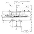
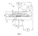
- FIG. 1is a schematic overview of a microelectronic component test system in accordance with an embodiment of the invention.
- FIG. 2is a schematic top view of a diagnostic card in accordance with one embodiment of the invention.
- FIG. 3is a schematic side view of the diagnostic card of FIG. 2 .
- FIG. 4is a schematic side view of the diagnostic card of FIGS. 2 and 3 in a first orientation in the test system of FIG. 1 .
- FIG. 5is a schematic side view similar to FIG. 4 , but showing the diagnostic card in a second orientation.
- FIG. 6is a graph schematically illustrating diagnostic test results for a test system with ideal planarity.
- FIG. 7is a graph schematically illustrating diagnostic test results for a test system which falls short of ideal relative planarity.
- FIG. 8is a schematic top view of the diagnostic card of FIGS. 2 and 3 juxtaposed with a contact surface of the test system of FIG. 4 .
- microelectronic component test systems and methodsfor verifying planarity of a head which holds a test card with respect to a microelectronic component support.
- microelectronic componentmay encompass a variety of articles of manufacture, including memory modules (e.g., SIMM, DRAM, or flash memory) ASICs, processors, semiconductor wafers, semiconductor dyes singulated from such wafers, assemblies of other microelectronic components, or any of a variety of other types of microelectronic devices or components therefor.
- program cardor “test card” may encompass a variety of architectures, including both rigid structures and flexible structures.
- the present inventionprovides a method of using a microelectronic component test system of the type which contacts a microelectronic component carried by a microelectronic component support with a plurality of test probes on a test card carried by a head.
- a contact memberis placed on the microelectronic component support.
- the contact membermay have a conductive contact surface of known planarity.
- a probe cardis mounted to the head such that the probe card is electrically coupled to the head and an array of probes carried by the probe card is oriented toward the contact member.
- the contact membermay move with respect to the probe card and a changing contact condition of each of the probes with respect to the contact surface may be recorded in a first data set.
- An orientation of the probe card with respect to the contact membermay be changed.
- the contact membermay be moved again with respect to the probe card and a change in contact condition of each of the probes with respect to the contact surface may be recorded in a second data set.
- An alternative embodimentprovides a method of testing a microelectronic component which involves a) determining a planarity characteristic of a microelectronic component support of a microelectronic component test system with respect to a head of the microelectronic component test system, and b) testing the microelectronic component with the microelectronic component test system (though not necessarily in that order).
- the planarity characteristicmay be determined by juxtaposing a diagnostic card with the microelectronic component support, thus orienting an array of diagnostic probes of the diagnostic card toward the microelectronic component support.
- the diagnostic probesmay be electrically coupled to the head.
- a distance between the diagnostic card and a contact surface carried by the microelectronic component supportis changed and a coordinate of the microelectronic component support at which each diagnostic probe changes a contact condition with respect to the contact surface may be recorded in a first data set.
- the first data setmay be processed with a processor of the test system to determine at least one planarity characteristic of the microelectronic component test system.
- Testing the microelectronic component with the test systemmay include electrically coupling test probes of a microelectronic component test card to the head of the microelectronic component test system. Terminals of the microelectronic component being tested are contacted with the test probes and test data for the microelectronic component may be collected in a conventional fashion.
- the test datamay be processed with the processor of the test system to determine at least one functional characteristic of the microelectronic component.
- a methodfor verifying planarity of a microelectronic component support with respect to a head of a microelectronic component test system.
- This methodincludes juxtaposing a probe card with a contact surface that is carried by the microelectronic component support, with probes of the probe card extending toward the contact surface. A distance along a Z axis between the probe card and the contact surface is changed. A Z coordinate of the contact surface at which each probe changes a contact condition with respect to a first location on the contact surface is recorded in a first data set. The probes may then be spaced from the contact surface and at least one of the probe card and the contact surface is translated with respect to an X-Y plane.
- a distance along the Z axis between the probe card and the contact surfacemay be changed.
- a Z coordinate of the contact surface at which each probe changes a contact condition with respect to a second location on the contact surface, which is spaced from the first location,may be recorded in a second data set.
- the first data set and the second data setmay be processed with a processor of the test system to determine a planarity characteristic.
- An alternative embodiment of the inventionprovides a microelectronic component test system.
- This test systemmay include a head, a microelectronic component support, and a programmable processor.
- the headis adapted to support a diagnostic card or a test card and be electrically coupled to diagnostic probes carried by the probe card or to test probes carried by the test card.
- the microelectronic component supportis adapted to carry a contact surface and to support a microelectronic component with respect to the head for testing.
- the programmable processoris operatively connected to the head to receive data from the head.
- the processoris programmed to record a first planarity data set corresponding to contact elevations of the diagnostic probes with a first location on the contact surface as a distance between the head and the microelectronic component support is changed.
- the processoris also programmed to record a second planarity data set corresponding to contact elevations of the diagnostic probes with a second location on the contact surface as a distance between the head and the microelectronic component support is changed; the first location is spaced from the second location.
- the processoris also programmed to compare the first data set and the second data set to determine at least one planarity characteristic of the microelectronic component test system.
- the processoralso may be programmed to record a test data set collected with the test contacts in electrical contact with terminals of a microelectronic component and to process the test data set to determine at least one functional characteristic of the microelectronic component.
- microelectronic component test systems and methodsin accordance with embodiments of the invention are best understood in light of the environment and equipment in which they can be used. Hence, one embodiment of a microelectronic component testing system which can be used in accordance with selected methods of the invention is initially described with reference to FIG. 1 . The details and features of several embodiments of diagnostic components and methods for verifying planarity are then described with reference to FIGS. 2-8 .
- FIG. 1schematically illustrates a microelectronic component test system 10 that may be used to test a microelectronic component 40 .
- the microelectronic component test system 10generally includes a microelectronic support 30 that supports a microelectronic component 40 with respect to a test card 50 , which is supported by a head 60 .
- the microelectronic support 30includes a generally flat, planar surface 32 and an actuator 34 for controllably moving the support surface 32 with respect to the head 60 .
- the actuator 34is adapted to move the support surface 32 along a Z axis to bring the microelectronic component 40 into electrical contact with the test card 50 .
- the actuator 34is also adapted to move the support surface 32 transversely with respect to the Z axis and the head 60 . As indicated by arrow X-Y, this may comprise movement in a plane which is generally perpendicular to the Z axis. (In the orientation shown in FIG. 1 , the Z axis is vertical and the X-Y plane is horizontal, but other orientations are possible.)
- the microelectronic support 30may also include adjustment screws 36 (shown schematically) or the like which can be used to alter the orientation of the support surface 32 with respect to the Z axis and/or the X-Y plane.
- these adjustment screws 36may comprise three or more finely threaded screws received in corresponding internally threaded holes carried by the upper element of the microelectronic support 30 .
- the support surface 32can be oriented perpendicular to the Z axis (horizontally in FIG. 1 ) by appropriate adjustment of one or more of the adjustment screws 36 .
- the support surface 32is adapted to support a microelectronic component 40 thereon.
- the microelectronic support 30may comprise a vacuum chuck. Such chucks, which are available commercially, can apply a vacuum on the back surface of the microelectronic component 40 to help hold the microelectronic component 40 in place as the actuator 34 moves the support surface 32 .
- the microelectronic component test system 10also includes a test card 50 which includes a plurality of test probes 52 positioned to contact terminals 42 on the microelectronic component 40 . As shown in FIG. 1 , when the test card 50 is juxtaposed with the microelectronic component 40 and the support surface 32 , the test probes 52 extend downwardly in a Z direction toward the terminals 42 .
- the test probes 52may be of any desired type. In one embodiment, the test probes 52 comprise wire pins or POGO PINS. In other embodiments, the test probes 52 may comprise cantilevered wires or the like.
- test probes 52may be electrically coupled to a test contact 54 by circuitry 56 (shown schematically). These test contacts 54 are arranged in an array which matches an array of head contacts 62 carried by the head 60 , permitting a wide variety of probe configurations to be coupled to the head contacts 62 , which may have a fixed position in the head 60 . This facilitates exchanging the test card 50 with a test card having a different probe arrangement to test different microelectronic component configurations.
- FIG. 1is a stylized, schematic representation of the interface between the test card 50 and the head 60 .
- the back of the test card 50will not be mounted flush against and supported by a bottom head surface 66 as depicted in FIG. 1 .
- the head 60may comprise a ring holder which has a central opening within which the test card 50 is received.
- ring holders and other suitable interfacesare well known in the art.
- a controller 70may be connected to the test probes 52 .
- the controller 70may communicate with the head contacts 62 (which, in turn, are in communication with the test probes 52 via the test contacts 54 and circuitry 56 ) by head circuitry 64 and a communication line 74 .
- the controller 70may take any of a variety of forms.
- the controller 70comprises a computer having a programmable processor 72 .
- the controller 30may be operatively coupled to a power supply 76 and control delivery of power from the power supply 76 to various components of the test card 50 via the communication line 74 .
- the actuator 34 of the microelectronic component support 30is operated directly by the controller 70 .
- a separate actuator control 78controls the actuator 34 , but the actuator control 78 communicates with the controller 70 and is operated under the control of the controller 70 .
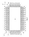
- FIGS. 2 and 3schematically illustrate a diagnostic probe card 100 in accordance with one embodiment.
- the diagnostic probe card 100includes a substrate 102 having a back surface 104 and a confronting surface 106 .
- the substrate 102is adapted to be supported by the head 60 of the test system 10 shown in FIG. 1 .
- the substrate 102may be formed of a variety of materials, but it preferably is formed of a relatively rigid and dimensionally stable material to maintain the relative positions of the ends of the probes carried by the substrate 102 .
- the substrate 102has a relatively low coefficient of thermal expansion. It is anticipated that most materials used in forming a conventional test card 50 may also be useful as the substrate 102 of the diagnostic probe card 100 .
- the substrate 102may comprise a ceramic or glass material.
- the substrate 102carries at least one probe 110 .
- the substratecarries a plurality of probes 110 - 125 arranged in an array.
- the arraymay be configured in any desired fashion.
- the arraymay include at least three probes to ascertain a plane of a contact surface of the test system 10 , as described below. Using four or more probes, e.g., four spaced-apart probes positioned adjacent corners of a rectangular substrate 102 , can further pinpoint the plane of the contact surface.
- the diagnostic probe card 100includes two sets of X probes 110 and 115 aligned in an X direction and two lines of Y probes 120 and 125 arranged in a Y direction.
- a plurality of first X probes 110 a-xare arranged adjacent a first edge 108 a of the substrate 102 .
- a line of second X probes 115 a-xare aligned adjacent an opposite side 108 b of the substrate 102 .
- first Y probes 120 a-hare aligned adjacent a third edge 108 c of the substrate 102 and the line of second Y probes 125 a-h are aligned adjacent an opposite fourth edge 108 d of the substrate 102 .
- first X-probes 110 amay be aligned parallel to the line of second X probes 115 and the first Y probes 120 may be aligned parallel to the line of second Y probes 125 .
- the diagnostic probe card 100 shown in FIGS. 2 and 3employs twenty-four first X probes 110 , twenty-four second X probes 115 , and eight each of the first Y probes 120 and the second Y probes 125 . As explained below, this provides extra redundancy and allows data collected with the probe card 100 to be processed to reduce the impact of “noise” in the data.
- FIG. 2schematically illustrates a pair of ground probes (designated GND) associated with each of the probes 110 - 125 .
- GNDground probes
- one of the probes in the pair of ground probes GNDis associated with a normally open channel of a relay (note shown) carried by the test head 60 and the other of the pair of ground probes GND is associated with a normally opened channel on the same relay in the head 60 .
- the probe card 100is first positioned in a first orientation with respect to the head 60 and is then positioned in a second orientation with respect to the head 60 .
- the probes 110 - 125may be positioned to be electrically coupled to the head contacts 62 of the head 60 .
- the ground probes GNDmay be positioned adjacent the edges 108 of the substrate 102 , generally in line with the lines of probes 110 - 125 , as shown in FIG. 2 .
- the ground probes GNDare positioned elsewhere on the substrate 102 at a location adapted to align with a corresponding head contact 62 .
- the probes 110 - 125may be aligned with an appropriate test contact.
- the ground probe normally associated with the normally closed switch on the relaymay be associated instead with the normally open switch and vice-versa.
- the probe 110 - 125 associated with the pair of ground probes GNDmay not be properly grounded. Switching the switch on the relay allows the probes 110 - 125 to be properly grounded in either orientation of the probe card 110 with respect to the head 60 .
- the dimensions of the probe card 100can be varied within a relatively wide range.
- the probe card 100may be a square or a non-rectangular polygon instead of the elongated rectangle shown in FIGS. 2 and 3 .
- Conventional test cards 50typically have the probes 52 arranged in a relatively small array adapted to contact a single microelectronic die or, perhaps, as many as four microelectronic dies.
- the diagnostic probe card 100need not be so limited in size. In one embodiment, the diagnostic probe card 100 has a length in the X direction of about 2.6 inches and a length in the Y direction of about 1.1 inches.
- the probes 110 - 125comprise conventional, commercially available spring-biased pins, such as POGO PINS, noted above. Other types of probes known in the art could be used, instead.
- each of the probesextends outwardly away from the confronting surface 106 of the substrate to a distal end spaced from the substrate. These distal ends desirably have a known relative relationship with respect to each other and to the confronting surface 106 of the substrate 102 .
- the tip of each of the probes 110is generally aligned with a plane P of known planarity.
- the plane Pis substantially parallel to the confronting surface 106 of the substrate 102 .
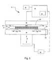
- FIG. 4schematically illustrates the diagnostic probe card 100 of FIGS. 2 and 3 positioned in the microelectronic component test system 10 discussed above in connection with FIG. 1 .
- the diagnostic probe card 100has replaced the test card 50 of FIG. 1 and the microelectronic component 40 of FIG. 1 has been replaced with a contact member 140 .
- the test head 60may have test contacts (omitted in FIG. 4 for purposes of clarity) which have fixed positions.
- the probe card 100may have contacts on the back surface 104 of the substrate 102 that are positioned to contact the head contacts 62 when the probe card 100 is mounted on the test head 60 .
- the array of head contacts 62may have a different arrangement from the rectangular arrangement shown in FIG. 2 . If so, the substrate 102 may function as a redistribution layer, including circuitry to electrically couple the probes 110 - 125 to appropriately positioned probe card contacts (not shown). This enables the relative planarity of the head 60 with respect to the support surface 32 of the microelectronic component support 30 to be determined without having to alter the head 60 to accommodate differences between the test card 50 and the probe card 100 .
- the planarity of the test system 10may be verified by bringing the probes 110 - 125 of the probe card 100 into contact with the support surface 32 of the microelectronic component support 30 , as discussed below.
- This contact surface 32may be somewhat irregular, though.
- the support surface 32may have ports formed therein to connect the backside of a microelectronic component 40 to a vacuum line to help hold the microelectronic component 40 in place.
- the support surface 32may also become scratched or otherwise damaged over time as many microelectronic components 40 are tested on the test system 10 .
- the probes 110 - 125 of the probe card 100are instead brought into contact with a contact member 140 carried by the microelectronic component support 30 .
- the contact member 140includes a first surface 142 and a second surface 144 .
- the first surface 142may be oriented toward the confronting surface 106 of the probe card 100 and the head surface 66 of the head 60 and the second surface 144 may be in supportive contact with the support surface 32 of the microelectronic component support 30 .
- the first surface 142has a known planarity.
- both the first surface 142 and the second surface 144are flat, smooth surfaces and the first and second surfaces 142 and 144 are highly parallel with respect to one another. This enables the probes 110 - 125 of the probe card 100 to be brought into contact with a surface which is known to be flat and has a known relationship with a plane defined by the contact surface 32 of the microelectronic component support 30 .
- the contact member 140can be formed of any suitable material.
- the materialis dimensionally stable, relatively rigid, and hard enough to avoid undue deformation when contacted with the probes 110 - 125 of the diagnostic probe card 100 . This will help maintain the desired degree of planarity of the first and surfaces 142 and 144 both individually and relative to one another.
- the test system 10is adapted to electrically determine a contact condition of each of the probes 110 - 125 with respect to the first surface 142 of the contact member 140 . This can be accomplished by providing a conductive coating on the first surface 142 , for example.
- the contact member 140may be formed of a conductive material.
- the contact member 140is formed of a relatively rigid, conductive metal, e.g., stainless steel.
- embodiments of the inventionprovide methods of using a microelectronic component test system and/or verifying planarity of elements of microelectronic component test systems.
- test system 10diagnostic probe card 100
- FIGS. 1-4the following discussion explains several such methods with reference to the test system 10 , diagnostic probe card 100 , and other elements of FIGS. 1-4 . It should be understood, however, that this is solely for purposes of illustration and the methods described below can be practiced with apparatus which differ materially from the structure shown in FIGS. 1-4 .
- the planarity of the component support 30 with respect to the head 60 of the test system 10may be checked from time to time. This may be done at regular intervals, when an operator suspects a planarity problem from trends in test data collected from microelectronic components, or when initially setting up a test system, for example.
- any test card 50 mounted to the head 60may be removed and a diagnostic probe card 100 may be mounted to the head 60 in its place. Mounting the probe card 100 to the head 60 will juxtapose the confronting surface 106 of the probe card 100 with the support surface 32 of the microelectronic component support 30 . As shown in FIG. 4 , the array of probes 110 - 125 thus may be oriented toward the microelectronic component support 30 .
- the probe card 100may be physically supported by the head 60 and electrically coupled to the same head contacts 62 to which the test contacts 52 of the test card 50 were coupled.
- the test system 10 shown in FIG. 4may be operated by contacting the probes 110 - 125 of the diagnostic probe card 100 with the support surface 32 of the microelectronic component support 30 .
- the probes 110 - 125are instead brought into contact with a surface 142 of a contact member 140 .
- Thiscan enhance the diagnosis of any planarity problems by using a surface 142 of known planarity, which may function as a conductive contact surface 142 for the probes 110 - 125 , rather than the possibly irregular support surface 32 .
- a contact member 140may be placed on the microelectronic component support 30 with its second surface 142 against the support surface 32 of the microelectronic component support 30 .
- the component support 30may be moved with respect to the probe card 100 and the controller 70 may record a change in contact condition of each of the probes 110 - 125 .
- moving the component support with respect to the probe card 100may involve changing a distance between the probe card 100 and a contact surface carried by the microelectronic component support (e.g., first surface 142 of the contact member 140 ).
- the probes 110 - 125will be spaced from the contact surface 142 .
- changing the distance between the probe card 100 and the contact surface 142may comprise moving the microelectronic component support 30 toward the head 60 with the actuator generally along the Z axis until some or all of the probes 110 - 125 contact the contact surface 142 .
- the controller 70may detect when each of the probes 110 - 125 establishes contact with the contact surface 142 .
- the microelectronic component support 30may be moved toward the head 60 until all of the probes 110 - 125 are in contact with the contact surface 142 ; if POGO PINS or the like are employed as the probes 110 - 125 , the probes may all be compressed to some degree.
- the distance between the microelectronic component support and the substrate 102 of the probe card 100may then be increased and the controller 70 may detect when each of the probes 110 - 125 breaks contact with the contact surface 142 .
- the microelectronic component support 30may be moved along the Z axis by a stepper motor (not shown) or the like of the actuator 34 .
- This actuator 34may be operated by the actuator control 78 of the controller 70 .
- the controller 70therefore, will have information relating to a position of the support surface 32 as the microelectronic component support 30 moves along the Z axis.
- the actuator 34moves the support surface 34 along the Z axis in small, fixed increments, e.g., 1 ⁇ m increments, and the contact condition of each of the probes 110 - 125 is checked to see if the contact condition of any of the probes has changed.
- the Z axis position of the microelectronic component support 30 when each probe changes its contact condition(e.g., establishes electrical contact or breaks electrical contact with the contact surface 142 ) can be recorded in a memory of the controller 70 in a first data set.
- the processor 72 of the controller 70may process the first data set to determine one or more planarity characteristics.
- the first data setmay comprise a Z axis coordinate for each of the probes 110 - 125 and the relative positions of the distal ends of the probes 110 - 125 in an X-Y direction may remain substantially constant.
- the first data setmay define a position in three-dimensional space at which each probe 110 - 125 first contacted the contact surface 142 .
- the processor 172may determine a best fit of a plane through these known positions and determine a relative planarity of the microelectronic component support surface 32 and the head 60 .
- the processor 72may process the first data set to determine any irregularities in the contact surface 142 ; this can be useful, for example, if the contact member 140 is omitted and the support surface 32 of the microelectronic component support 30 functions as the contact surface. This provides a simple, automated procedure for determining the relative planarity of the microelectronic component support 30 and the head 60 .
- One conventional approach to measuring planarity of a conventional test systeminvolves lifting the head of the system out of the way and running a distance gage over the support surface of the microelectronic component support. This may identify deviations in planarity of the support surface, but it will not readily identify planarity deviations of the head. Additionally, lifting the head to permit access by the distance gage often requires breaking electrical contact between the head and the test system controller. Breaking and reestablishing electrical contact may temporarily correct an intermittent electrical short without diagnosing the problem.
- Embodiments which employ a diagnostic probe card 100 having contacts arranged in an array which corresponds with the array of head contacts 62 ( FIG. 1 )allows the diagnostic probe card 100 to be mounted to the head 60 in much the same fashion as are the test cards 50 . Consequently, the first data set can be collected without unduly disturbing the orientation of the head 60 and the support 30 , enhancing repeatability of the diagnostic information and extrapolation of the diagnostic information to conditions of the test system 10 with the test card 50 in place.
- mounting the probe card 100 to the head 60 in such embodimentscan better reproduce the relative position of the test card 50 with respect to the microelectronic component support 30 .
- the test system 10is used to collect at least a second data set, with an orientation of the diagnostic probe card 100 with respect to the contact surface differing between the first and second data sets.
- FIG. 5schematically illustrates one reconfiguration of the test system 10 .
- the probe card 100is oriented differently in FIG. 5 than in FIG. 4 .
- the probe card 100is oriented in a first orientation with respect to the microelectronic component support 30 in which the first X probes 110 are in the foreground and the second X probes 115 are hidden behind the first X probes 110 .
- FIG. 4schematically illustrates one reconfiguration of the test system 10 .
- the probe card 100is oriented differently in FIG. 5 than in FIG. 4 .
- the probe card 100is oriented in a first orientation with respect to the microelectronic component support 30 in which the first X probes 110 are in the foreground and the second X probes 115 are hidden behind the first X probes 110 .
- the probe card 100is oriented in a second orientation with respect to the microelectronic component support 30 in which the second X probes 115 are in the foreground and the first X probes 110 are hidden behind the second X probes 115 .
- the probe card 100In changing the probe card orientation from FIG. 4 to FIG. 5 , the probe card 100 remains juxtaposed with the same location on the contact surface 142 , i.e., the center of the contact surface 142 . This can be accomplished by turning the probe card 100 180° in the X-Y plane with respect to the contact surface 142 . In one embodiment, the probe card 100 is removed from the head 60 , rotated 180° within a horizontal plane of the probe card 100 (i.e., a plane of the substrate 102 ), and remounted to the head 60 in the orientation shown in FIG. 5 .
- thismay require adjusting relays or the like to ensure that the probes 110 - 125 are compared to an associated grounded probe (one of the pair of contacts GND in FIG. 2 ).
- the probe card 100remains stationary and the microelectronic component support 30 is turned 180° about its axis.
- FIGS. 6 and 7schematically depict idealized data collected in this fashion.
- FIG. 6illustrates the measurements anticipated for a linear array of probes (e.g., the first X probes 110 ) of an ideal probe card 100 with an ideally planar test system 10 .
- the X axisrepresents the relative position of each of the probes 10 on the probe card and the Z axis represents a Z coordinate corresponding to a change in contact condition for each probe.
- the first data setis represented by plus signs and the second data set, with the probe card 100 turned 180°, is represented by Xs.
- the Z coordinateis identical for each of the probes, regardless of the orientation of the probe card. Consequently, the line defined by this linear array of probes 110 defines a horizontal line 200 .
- Each of the other sets of probes 115 , 120 , and 125would similarly yield a horizontal line and plotting the points in three dimensions would describe a horizontal plane.
- FIG. 7schematically depicts results which may be obtained with a less idealized system.
- a first sloped line 210may represent a linear regression of the first data set and a second sloped line 220 may represent a linear regression of the second data set. If the distal tips of the probes 110 were aligned in a precisely horizontal plane, each of the sloped lines 210 and 220 would have a slope which corresponds to a relative planarity of the microelectronic component support 30 with respect to the head 60 .
- a line 230 bisecting these two sloped lines 210 and 220would be precisely horizontal and the maximum difference between the two lines 210 and 220 (at the ends of the lines) would represent a quantitative assessment of a maximum planarity deviation.
- this maximum planarity deviationis greater than a predetermined maximum, an error condition may be flagged and an error warning may be generated.
- the line 230 bisecting the angle between the two sloped lines 210 and 220is also sloped. This indicates a non-linear bias of the line of probes 110 . Determining the bias in this fashion allows imperfections of the probe card 100 to be identified and quantitatively factored out of the measured planarity characteristics.
- FIG. 7represents a line of data collected with the linearly aligned first X probes 110 .
- the controller 70also gives the operator quantitative planarity data (e.g., by a graphical display) that the operator may use as a guide to adjust the microelectronic component support 30 and/or the head 60 to improve planarity of the test system.
- changing the orientation of the diagnostic probe card 100 with respect to the contact surface 142may comprise moving the probe card from a first location on the contact surface 142 to a second location on the contact surface 142 spaced in an X-Y plane from the first location.
- the probe card 100may be juxtaposed with a first location 142 a on the contact surface and a first data set may be collected, as described above.
- the actuator 34 of the microelectronic component support 30FIGS.
- a third data setmay be collected for a third contact surface location 142 c
- a fourth data setmay be collected for a fourth contact surface location 142 d
- a fifth data setmay be collected for a fifth contact surface location 142 e.
- Collecting data sets with an array of probes at multiple locationsenables a determination of a planarity of the head and a planarity of the support surface 32 in addition to a relative planarity measurement. If one data set describes a sloped plane, one would only know that one or both of the head 60 and the support 30 is not parallel o the X-Y plane.
- a mean Z coordinate valuecan be calculated for each of the five data sets for the five locations 142 a-e . If each of these data sets describes a similarly sloped plane, but the mean Z value is substantially the same for all five data sets, this is an indication that the test head 60 is not planar with respect to the X-Y plane. Additionally, the determined slope of the plane can be used as a quantitative guide in adjusting the head 60 , providing both an indication of the slope of the head 60 and an orientation of the slope to indicate which side of the head should be raised or lowered.
- each of the data setsdescribes a similarly sloped plane but the mean Z value differs between the five locations 142 a-e , this will indicate that the support surface 32 is not parallel with the X-Y plane. Since the five data sets are collected at known locations 142 a-e , the change in mean Z value between the five data sets will provide quantitative data suggesting what side of the support surface 32 should be raised or lowered and how far.
- two data setsmay be collected at one or more of the five contact surface locations 142 a-e , with the orientation of the probe card 100 being different for the two data sets for each site. As noted above, this can further refine the process by enabling the processor 72 to factor out any defects in the probe card 100 . In one embodiment, two such data sets are collected for the first contact surface location 142 a , but only a single set of data is collected for each of the other contact surface locations 142 b-e.
Landscapes
- Engineering & Computer Science (AREA)
- Physics & Mathematics (AREA)
- General Physics & Mathematics (AREA)
- Computer Hardware Design (AREA)
- Microelectronics & Electronic Packaging (AREA)
- General Engineering & Computer Science (AREA)
- Power Engineering (AREA)
- Testing Or Measuring Of Semiconductors Or The Like (AREA)
- Measuring Leads Or Probes (AREA)
Abstract
Description
Claims (19)
Priority Applications (4)
| Application Number | Priority Date | Filing Date | Title |
|---|---|---|---|
| US10/230,615US6841991B2 (en) | 2002-08-29 | 2002-08-29 | Planarity diagnostic system, E.G., for microelectronic component test systems |
| US10/930,647US7019512B2 (en) | 2002-08-29 | 2004-08-31 | Planarity diagnostic system, e.g., for microelectronic component test systems |
| US11/343,502US7211997B2 (en) | 2002-08-29 | 2006-01-30 | Planarity diagnostic system, E.G., for microelectronic component test systems |
| US11/623,505US7253608B2 (en) | 2002-08-29 | 2007-01-16 | Planarity diagnostic system, e.g., for microelectronic component test systems |
Applications Claiming Priority (1)
| Application Number | Priority Date | Filing Date | Title |
|---|---|---|---|
| US10/230,615US6841991B2 (en) | 2002-08-29 | 2002-08-29 | Planarity diagnostic system, E.G., for microelectronic component test systems |
Related Child Applications (1)
| Application Number | Title | Priority Date | Filing Date |
|---|---|---|---|
| US10/930,647DivisionUS7019512B2 (en) | 2002-08-29 | 2004-08-31 | Planarity diagnostic system, e.g., for microelectronic component test systems |
Publications (2)
| Publication Number | Publication Date |
|---|---|
| US20040041556A1 US20040041556A1 (en) | 2004-03-04 |
| US6841991B2true US6841991B2 (en) | 2005-01-11 |
Family
ID=31976532
Family Applications (4)
| Application Number | Title | Priority Date | Filing Date |
|---|---|---|---|
| US10/230,615Expired - Fee RelatedUS6841991B2 (en) | 2002-08-29 | 2002-08-29 | Planarity diagnostic system, E.G., for microelectronic component test systems |
| US10/930,647Expired - Fee RelatedUS7019512B2 (en) | 2002-08-29 | 2004-08-31 | Planarity diagnostic system, e.g., for microelectronic component test systems |
| US11/343,502Expired - Fee RelatedUS7211997B2 (en) | 2002-08-29 | 2006-01-30 | Planarity diagnostic system, E.G., for microelectronic component test systems |
| US11/623,505Expired - Fee RelatedUS7253608B2 (en) | 2002-08-29 | 2007-01-16 | Planarity diagnostic system, e.g., for microelectronic component test systems |
Family Applications After (3)
| Application Number | Title | Priority Date | Filing Date |
|---|---|---|---|
| US10/930,647Expired - Fee RelatedUS7019512B2 (en) | 2002-08-29 | 2004-08-31 | Planarity diagnostic system, e.g., for microelectronic component test systems |
| US11/343,502Expired - Fee RelatedUS7211997B2 (en) | 2002-08-29 | 2006-01-30 | Planarity diagnostic system, E.G., for microelectronic component test systems |
| US11/623,505Expired - Fee RelatedUS7253608B2 (en) | 2002-08-29 | 2007-01-16 | Planarity diagnostic system, e.g., for microelectronic component test systems |
Country Status (1)
| Country | Link |
|---|---|
| US (4) | US6841991B2 (en) |
Cited By (10)
| Publication number | Priority date | Publication date | Assignee | Title |
|---|---|---|---|---|
| US20050024040A1 (en)* | 2002-08-29 | 2005-02-03 | Martin Michael H. | Planarity diagnostic system, e.g., for microelectronic component test systems |
| US20050099196A1 (en)* | 2003-11-12 | 2005-05-12 | Nec Electronics Corporation | Semiconductor inspection device based on use of probe information, and semiconductor inspection method |
| US20060214679A1 (en)* | 2005-03-28 | 2006-09-28 | Formfactor, Inc. | Active diagnostic interface for wafer probe applications |
| US20060236170A1 (en)* | 2005-04-19 | 2006-10-19 | Micron Technology, Inc. | On-chip sampling circuit and method |
| US20070103181A1 (en)* | 2003-03-14 | 2007-05-10 | Applied Precision, Llc | System and method of mitigating effects of component deflection in a probe card analyzer |
| US20080044623A1 (en)* | 2006-08-21 | 2008-02-21 | John Caldwell | Probe card for testing imaging devices, and methods of fabricating same |
| US20080100312A1 (en)* | 2006-11-01 | 2008-05-01 | Formfactor, Inc. | Method And Apparatus For Providing Active Compliance In A Probe Card Assembly |
| US20090261517A1 (en)* | 2008-04-21 | 2009-10-22 | Formfactor, Inc. | Multi-stage spring system |
| US20100231249A1 (en)* | 2009-03-12 | 2010-09-16 | Dang Son N | Probe Head Structure For Probe Test Cards |
| US20150015299A1 (en)* | 2012-04-09 | 2015-01-15 | Advanced Inquiry Systems, Inc. | Translators coupleable to opposing surfaces of microelectronic substrates for testing, and associated systems and methods |
Families Citing this family (9)
| Publication number | Priority date | Publication date | Assignee | Title |
|---|---|---|---|---|
| US7572169B1 (en)* | 1998-11-06 | 2009-08-11 | Beaver Creek Concepts Inc | Advanced finishing control |
| KR100568537B1 (en)* | 2003-06-24 | 2006-04-07 | 삼성전자주식회사 | Buffered memory module |
| CN101126626B (en)* | 2006-08-18 | 2010-09-22 | 鸿富锦精密工业(深圳)有限公司 | Flatness tester |
| US7750657B2 (en)* | 2007-03-15 | 2010-07-06 | Applied Materials Inc. | Polishing head testing with movable pedestal |
| US7639777B2 (en)* | 2008-02-26 | 2009-12-29 | United Technologies Corp. | Computed tomography systems and related methods involving forward collimation |
| TWI528876B (en)* | 2012-03-22 | 2016-04-01 | 矽品精密工業股份有限公司 | Medium board and its electrical testing method |
| US9116165B2 (en)* | 2012-03-27 | 2015-08-25 | Freescale Semiconductor, Inc. | Microelectromechanical system package and method of testing |
| US9766269B2 (en)* | 2012-12-29 | 2017-09-19 | Power Probe TEK, LLC | Conductive test probe |
| JP6592885B2 (en)* | 2014-10-08 | 2019-10-23 | 日本電産リード株式会社 | Substrate inspection method and substrate inspection apparatus |
Citations (82)
| Publication number | Priority date | Publication date | Assignee | Title |
|---|---|---|---|---|
| US4751457A (en)* | 1986-09-08 | 1988-06-14 | Tektronix, Inc. | Integrated circuit probe parallelism establishing method and apparatus |
| US4918374A (en)* | 1988-10-05 | 1990-04-17 | Applied Precision, Inc. | Method and apparatus for inspecting integrated circuit probe cards |
| US5065092A (en)* | 1990-05-14 | 1991-11-12 | Triple S Engineering, Inc. | System for locating probe tips on an integrated circuit probe card and method therefor |
| US5069002A (en) | 1991-04-17 | 1991-12-03 | Micron Technology, Inc. | Apparatus for endpoint detection during mechanical planarization of semiconductor wafers |
| US5081796A (en) | 1990-08-06 | 1992-01-21 | Micron Technology, Inc. | Method and apparatus for mechanical planarization and endpoint detection of a semiconductor wafer |
| US5232875A (en) | 1992-10-15 | 1993-08-03 | Micron Technology, Inc. | Method and apparatus for improving planarity of chemical-mechanical planarization operations |
| US5234867A (en) | 1992-05-27 | 1993-08-10 | Micron Technology, Inc. | Method for planarizing semiconductor wafers with a non-circular polishing pad |
| US5240552A (en) | 1991-12-11 | 1993-08-31 | Micron Technology, Inc. | Chemical mechanical planarization (CMP) of a semiconductor wafer using acoustical waves for in-situ end point detection |
| US5244534A (en) | 1992-01-24 | 1993-09-14 | Micron Technology, Inc. | Two-step chemical mechanical polishing process for producing flush and protruding tungsten plugs |
| US5245796A (en) | 1992-04-02 | 1993-09-21 | At&T Bell Laboratories | Slurry polisher using ultrasonic agitation |
| US5245790A (en) | 1992-02-14 | 1993-09-21 | Lsi Logic Corporation | Ultrasonic energy enhanced chemi-mechanical polishing of silicon wafers |
| US5433651A (en) | 1993-12-22 | 1995-07-18 | International Business Machines Corporation | In-situ endpoint detection and process monitoring method and apparatus for chemical-mechanical polishing |
| US5449314A (en) | 1994-04-25 | 1995-09-12 | Micron Technology, Inc. | Method of chimical mechanical polishing for dielectric layers |
| US5486129A (en) | 1993-08-25 | 1996-01-23 | Micron Technology, Inc. | System and method for real-time control of semiconductor a wafer polishing, and a polishing head |
| US5514245A (en) | 1992-01-27 | 1996-05-07 | Micron Technology, Inc. | Method for chemical planarization (CMP) of a semiconductor wafer to provide a planar surface free of microscratches |
| US5533924A (en) | 1994-09-01 | 1996-07-09 | Micron Technology, Inc. | Polishing apparatus, a polishing wafer carrier apparatus, a replacable component for a particular polishing apparatus and a process of polishing wafers |
| US5540810A (en) | 1992-12-11 | 1996-07-30 | Micron Technology Inc. | IC mechanical planarization process incorporating two slurry compositions for faster material removal times |
| US5618381A (en) | 1992-01-24 | 1997-04-08 | Micron Technology, Inc. | Multiple step method of chemical-mechanical polishing which minimizes dishing |
| US5642056A (en)* | 1993-12-22 | 1997-06-24 | Tokyo Electron Limited | Probe apparatus for correcting the probe card posture before testing |
| US5643060A (en) | 1993-08-25 | 1997-07-01 | Micron Technology, Inc. | System for real-time control of semiconductor wafer polishing including heater |
| US5658190A (en) | 1995-12-15 | 1997-08-19 | Micron Technology, Inc. | Apparatus for separating wafers from polishing pads used in chemical-mechanical planarization of semiconductor wafers |
| US5658183A (en) | 1993-08-25 | 1997-08-19 | Micron Technology, Inc. | System for real-time control of semiconductor wafer polishing including optical monitoring |
| US5679065A (en) | 1996-02-23 | 1997-10-21 | Micron Technology, Inc. | Wafer carrier having carrier ring adapted for uniform chemical-mechanical planarization of semiconductor wafers |
| US5702292A (en) | 1996-10-31 | 1997-12-30 | Micron Technology, Inc. | Apparatus and method for loading and unloading substrates to a chemical-mechanical planarization machine |
| US5747386A (en) | 1996-10-03 | 1998-05-05 | Micron Technology, Inc. | Rotary coupling |
| US5761823A (en) | 1994-09-27 | 1998-06-09 | Williamson, Jr.; John S. | Relative planarity verification apparatus and method of use |
| US5792709A (en) | 1995-12-19 | 1998-08-11 | Micron Technology, Inc. | High-speed planarizing apparatus and method for chemical mechanical planarization of semiconductor wafers |
| US5795495A (en) | 1994-04-25 | 1998-08-18 | Micron Technology, Inc. | Method of chemical mechanical polishing for dielectric layers |
| US5807165A (en) | 1997-03-26 | 1998-09-15 | International Business Machines Corporation | Method of electrochemical mechanical planarization |
| US5830806A (en) | 1996-10-18 | 1998-11-03 | Micron Technology, Inc. | Wafer backing member for mechanical and chemical-mechanical planarization of substrates |
| US5851135A (en) | 1993-08-25 | 1998-12-22 | Micron Technology, Inc. | System for real-time control of semiconductor wafer polishing |
| US5868896A (en) | 1996-11-06 | 1999-02-09 | Micron Technology, Inc. | Chemical-mechanical planarization machine and method for uniformly planarizing semiconductor wafers |
| US5893754A (en) | 1996-05-21 | 1999-04-13 | Micron Technology, Inc. | Method for chemical-mechanical planarization of stop-on-feature semiconductor wafers |
| US5895550A (en) | 1996-12-16 | 1999-04-20 | Micron Technology, Inc. | Ultrasonic processing of chemical mechanical polishing slurries |
| US5934980A (en) | 1997-06-09 | 1999-08-10 | Micron Technology, Inc. | Method of chemical mechanical polishing |
| US5945347A (en) | 1995-06-02 | 1999-08-31 | Micron Technology, Inc. | Apparatus and method for polishing a semiconductor wafer in an overhanging position |
| US5967030A (en) | 1995-11-17 | 1999-10-19 | Micron Technology, Inc. | Global planarization method and apparatus |
| US5972792A (en) | 1996-10-18 | 1999-10-26 | Micron Technology, Inc. | Method for chemical-mechanical planarization of a substrate on a fixed-abrasive polishing pad |
| US5980363A (en) | 1996-06-13 | 1999-11-09 | Micron Technology, Inc. | Under-pad for chemical-mechanical planarization of semiconductor wafers |
| US5997384A (en) | 1997-12-22 | 1999-12-07 | Micron Technology, Inc. | Method and apparatus for controlling planarizing characteristics in mechanical and chemical-mechanical planarization of microelectronic substrates |
| US6039633A (en) | 1998-10-01 | 2000-03-21 | Micron Technology, Inc. | Method and apparatus for mechanical and chemical-mechanical planarization of microelectronic-device substrate assemblies |
| US6043668A (en) | 1997-12-12 | 2000-03-28 | Sony Corporation | Planarity verification system for integrated circuit test probes |
| US6066030A (en) | 1999-03-04 | 2000-05-23 | International Business Machines Corporation | Electroetch and chemical mechanical polishing equipment |
| US6074286A (en) | 1998-01-05 | 2000-06-13 | Micron Technology, Inc. | Wafer processing apparatus and method of processing a wafer utilizing a processing slurry |
| US6083085A (en) | 1997-12-22 | 2000-07-04 | Micron Technology, Inc. | Method and apparatus for planarizing microelectronic substrates and conditioning planarizing media |
| US6110820A (en) | 1995-06-07 | 2000-08-29 | Micron Technology, Inc. | Low scratch density chemical mechanical planarization process |
| US6135856A (en) | 1996-01-19 | 2000-10-24 | Micron Technology, Inc. | Apparatus and method for semiconductor planarization |
| US6139402A (en) | 1997-12-30 | 2000-10-31 | Micron Technology, Inc. | Method and apparatus for mechanical and chemical-mechanical planarization of microelectronic substrates |
| US6143155A (en) | 1998-06-11 | 2000-11-07 | Speedfam Ipec Corp. | Method for simultaneous non-contact electrochemical plating and planarizing of semiconductor wafers using a bipiolar electrode assembly |
| US6152808A (en) | 1998-08-25 | 2000-11-28 | Micron Technology, Inc. | Microelectronic substrate polishing systems, semiconductor wafer polishing systems, methods of polishing microelectronic substrates, and methods of polishing wafers |
| US6176992B1 (en) | 1998-11-03 | 2001-01-23 | Nutool, Inc. | Method and apparatus for electro-chemical mechanical deposition |
| US6187681B1 (en) | 1998-10-14 | 2001-02-13 | Micron Technology, Inc. | Method and apparatus for planarization of a substrate |
| US6191037B1 (en) | 1998-09-03 | 2001-02-20 | Micron Technology, Inc. | Methods, apparatuses and substrate assembly structures for fabricating microelectronic components using mechanical and chemical-mechanical planarization processes |
| US6193588B1 (en) | 1998-09-02 | 2001-02-27 | Micron Technology, Inc. | Method and apparatus for planarizing and cleaning microelectronic substrates |
| US6200901B1 (en) | 1998-06-10 | 2001-03-13 | Micron Technology, Inc. | Polishing polymer surfaces on non-porous CMP pads |
| US6203404B1 (en) | 1999-06-03 | 2001-03-20 | Micron Technology, Inc. | Chemical mechanical polishing methods |
| US6203413B1 (en) | 1999-01-13 | 2001-03-20 | Micron Technology, Inc. | Apparatus and methods for conditioning polishing pads in mechanical and/or chemical-mechanical planarization of microelectronic-device substrate assemblies |
| US6206756B1 (en) | 1998-11-10 | 2001-03-27 | Micron Technology, Inc. | Tungsten chemical-mechanical polishing process using a fixed abrasive polishing pad and a tungsten layer chemical-mechanical polishing solution specifically adapted for chemical-mechanical polishing with a fixed abrasive pad |
| US6210257B1 (en) | 1998-05-29 | 2001-04-03 | Micron Technology, Inc. | Web-format polishing pads and methods for manufacturing and using web-format polishing pads in mechanical and chemical-mechanical planarization of microelectronic substrates |
| US6213845B1 (en) | 1999-04-26 | 2001-04-10 | Micron Technology, Inc. | Apparatus for in-situ optical endpointing on web-format planarizing machines in mechanical or chemical-mechanical planarization of microelectronic-device substrate assemblies and methods for making and using same |
| US6218316B1 (en) | 1998-10-22 | 2001-04-17 | Micron Technology, Inc. | Planarization of non-planar surfaces in device fabrication |
| US6227955B1 (en) | 1999-04-20 | 2001-05-08 | Micron Technology, Inc. | Carrier heads, planarizing machines and methods for mechanical or chemical-mechanical planarization of microelectronic-device substrate assemblies |
| US6234878B1 (en) | 1999-08-31 | 2001-05-22 | Micron Technology, Inc. | Endpoint detection apparatus, planarizing machines with endpointing apparatus, and endpointing methods for mechanical or chemical-mechanical planarization of microelectronic substrate assemblies |
| US6250994B1 (en) | 1998-10-01 | 2001-06-26 | Micron Technology, Inc. | Methods and apparatuses for mechanical and chemical-mechanical planarization of microelectronic-device substrate assemblies on planarizing pads |
| US6261163B1 (en) | 1999-08-30 | 2001-07-17 | Micron Technology, Inc. | Web-format planarizing machines and methods for planarizing microelectronic substrate assemblies |
| US6267650B1 (en) | 1999-08-09 | 2001-07-31 | Micron Technology, Inc. | Apparatus and methods for substantial planarization of solder bumps |
| US6273796B1 (en) | 1999-09-01 | 2001-08-14 | Micron Technology, Inc. | Method and apparatus for planarizing a microelectronic substrate with a tilted planarizing surface |
| US6276996B1 (en) | 1998-11-10 | 2001-08-21 | Micron Technology, Inc. | Copper chemical-mechanical polishing process using a fixed abrasive polishing pad and a copper layer chemical-mechanical polishing solution specifically adapted for chemical-mechanical polishing with a fixed abrasive pad |
| US6306012B1 (en) | 1999-07-20 | 2001-10-23 | Micron Technology, Inc. | Methods and apparatuses for planarizing microelectronic substrate assemblies |
| US6306768B1 (en) | 1999-11-17 | 2001-10-23 | Micron Technology, Inc. | Method for planarizing microelectronic substrates having apertures |
| US6328632B1 (en) | 1999-08-31 | 2001-12-11 | Micron Technology, Inc. | Polishing pads and planarizing machines for mechanical and/or chemical-mechanical planarization of microelectronic substrate assemblies |
| US6331488B1 (en) | 1997-05-23 | 2001-12-18 | Micron Technology, Inc. | Planarization process for semiconductor substrates |
| US6350180B2 (en) | 1999-08-31 | 2002-02-26 | Micron Technology, Inc. | Methods for predicting polishing parameters of polishing pads, and methods and machines for planarizing microelectronic substrate assemblies in mechanical or chemical-mechanical planarization |
| US6352466B1 (en) | 1998-08-31 | 2002-03-05 | Micron Technology, Inc. | Method and apparatus for wireless transfer of chemical-mechanical planarization measurements |
| US6359456B1 (en) | 1997-02-11 | 2002-03-19 | Micron Technology, Inc. | Probe card and test system for semiconductor wafers |
| US6358129B2 (en) | 1998-11-11 | 2002-03-19 | Micron Technology, Inc. | Backing members and planarizing machines for mechanical and chemical-mechanical planarization of microelectronic-device substrate assemblies, and methods of making and using such backing members |
| US6358122B1 (en) | 1999-08-31 | 2002-03-19 | Micron Technology, Inc. | Method and apparatus for mechanical and chemical-mechanical planarization of microelectronic substrates with metal compound abrasives |
| US6361417B2 (en) | 1999-08-31 | 2002-03-26 | Micron Technology, Inc. | Method and apparatus for supporting a polishing pad during chemical-mechanical planarization of microelectronic substrates |
| US6368190B1 (en) | 2000-01-26 | 2002-04-09 | Agere Systems Guardian Corp. | Electrochemical mechanical planarization apparatus and method |
| US6368197B2 (en) | 1999-08-31 | 2002-04-09 | Micron Technology, Inc. | Method and apparatus for supporting and cleaning a polishing pad for chemical-mechanical planarization of microelectronic substrates |
| US6368194B1 (en) | 1998-07-23 | 2002-04-09 | Micron Technology, Inc. | Apparatus for controlling PH during planarization and cleaning of microelectronic substrates |
| US6496001B1 (en)* | 2000-11-14 | 2002-12-17 | International Business Machines Corporation | System and method for probe mechanism planarization |
Family Cites Families (23)
| Publication number | Priority date | Publication date | Assignee | Title |
|---|---|---|---|---|
| US6125255A (en) | 1996-09-23 | 2000-09-26 | Xerox Corporation | Magnet assembly with inserts and method of manufacturing |
| US6395620B1 (en)* | 1996-10-08 | 2002-05-28 | Micron Technology, Inc. | Method for forming a planar surface over low density field areas on a semiconductor wafer |
| DE19754544C1 (en)* | 1997-12-09 | 1999-07-01 | Roland Man Druckmasch | Rotary printing machine |
| US6111419A (en)* | 1998-05-19 | 2000-08-29 | Motorola Inc. | Method of processing a substrate including measuring for planarity and probing the substrate |
| KR100326270B1 (en) | 1998-12-24 | 2002-05-09 | 박종섭 | Semiconductor memory device using one common address bus line between address buffers and column predecoder |
| US6599836B1 (en)* | 1999-04-09 | 2003-07-29 | Micron Technology, Inc. | Planarizing solutions, planarizing machines and methods for mechanical or chemical-mechanical planarization of microelectronic-device substrate assemblies |
| US6383934B1 (en)* | 1999-09-02 | 2002-05-07 | Micron Technology, Inc. | Method and apparatus for chemical-mechanical planarization of microelectronic substrates with selected planarizing liquids |
| US6498101B1 (en) | 2000-02-28 | 2002-12-24 | Micron Technology, Inc. | Planarizing pads, planarizing machines and methods for making and using planarizing pads in mechanical and chemical-mechanical planarization of microelectronic device substrate assemblies |
| US6290572B1 (en)* | 2000-03-23 | 2001-09-18 | Micron Technology, Inc. | Devices and methods for in-situ control of mechanical or chemical-mechanical planarization of microelectronic-device substrate assemblies |
| US6313038B1 (en)* | 2000-04-26 | 2001-11-06 | Micron Technology, Inc. | Method and apparatus for controlling chemical interactions during planarization of microelectronic substrates |
| US6387289B1 (en)* | 2000-05-04 | 2002-05-14 | Micron Technology, Inc. | Planarizing machines and methods for mechanical and/or chemical-mechanical planarization of microelectronic-device substrate assemblies |
| US6428386B1 (en)* | 2000-06-16 | 2002-08-06 | Micron Technology, Inc. | Planarizing pads, planarizing machines, and methods for mechanical and/or chemical-mechanical planarization of microelectronic-device substrate assemblies |
| US6520834B1 (en)* | 2000-08-09 | 2003-02-18 | Micron Technology, Inc. | Methods and apparatuses for analyzing and controlling performance parameters in mechanical and chemical-mechanical planarization of microelectronic substrates |
| US6592443B1 (en)* | 2000-08-30 | 2003-07-15 | Micron Technology, Inc. | Method and apparatus for forming and using planarizing pads for mechanical and chemical-mechanical planarization of microelectronic substrates |
| US6447369B1 (en) | 2000-08-30 | 2002-09-10 | Micron Technology, Inc. | Planarizing machines and alignment systems for mechanical and/or chemical-mechanical planarization of microelectronic substrates |
| US6609947B1 (en)* | 2000-08-30 | 2003-08-26 | Micron Technology, Inc. | Planarizing machines and control systems for mechanical and/or chemical-mechanical planarization of micro electronic substrates |
| US6623329B1 (en) | 2000-08-31 | 2003-09-23 | Micron Technology, Inc. | Method and apparatus for supporting a microelectronic substrate relative to a planarization pad |
| US6652764B1 (en) | 2000-08-31 | 2003-11-25 | Micron Technology, Inc. | Methods and apparatuses for making and using planarizing pads for mechanical and chemical-mechanical planarization of microelectronic substrates |
| US6558190B1 (en)* | 2000-10-24 | 2003-05-06 | Worldcom, Inc. | Method and system of an installer-friendly, modularly adaptable, electrical, outlet gang box |
| US6762612B2 (en)* | 2001-06-20 | 2004-07-13 | Advantest Corp. | Probe contact system having planarity adjustment mechanism |
| US6677771B2 (en)* | 2001-06-20 | 2004-01-13 | Advantest Corp. | Probe contact system having planarity adjustment mechanism |
| US6666749B2 (en) | 2001-08-30 | 2003-12-23 | Micron Technology, Inc. | Apparatus and method for enhanced processing of microelectronic workpieces |
| US6841991B2 (en)* | 2002-08-29 | 2005-01-11 | Micron Technology, Inc. | Planarity diagnostic system, E.G., for microelectronic component test systems |
- 2002
- 2002-08-29USUS10/230,615patent/US6841991B2/ennot_activeExpired - Fee Related
- 2004
- 2004-08-31USUS10/930,647patent/US7019512B2/ennot_activeExpired - Fee Related
- 2006
- 2006-01-30USUS11/343,502patent/US7211997B2/ennot_activeExpired - Fee Related
- 2007
- 2007-01-16USUS11/623,505patent/US7253608B2/ennot_activeExpired - Fee Related
Patent Citations (108)
| Publication number | Priority date | Publication date | Assignee | Title |
|---|---|---|---|---|
| US4751457A (en)* | 1986-09-08 | 1988-06-14 | Tektronix, Inc. | Integrated circuit probe parallelism establishing method and apparatus |
| US4918374A (en)* | 1988-10-05 | 1990-04-17 | Applied Precision, Inc. | Method and apparatus for inspecting integrated circuit probe cards |
| US5421769A (en) | 1990-01-22 | 1995-06-06 | Micron Technology, Inc. | Apparatus for planarizing semiconductor wafers, and a polishing pad for a planarization apparatus |
| US5065092A (en)* | 1990-05-14 | 1991-11-12 | Triple S Engineering, Inc. | System for locating probe tips on an integrated circuit probe card and method therefor |
| US5081796A (en) | 1990-08-06 | 1992-01-21 | Micron Technology, Inc. | Method and apparatus for mechanical planarization and endpoint detection of a semiconductor wafer |
| US5069002A (en) | 1991-04-17 | 1991-12-03 | Micron Technology, Inc. | Apparatus for endpoint detection during mechanical planarization of semiconductor wafers |
| US5240552A (en) | 1991-12-11 | 1993-08-31 | Micron Technology, Inc. | Chemical mechanical planarization (CMP) of a semiconductor wafer using acoustical waves for in-situ end point detection |
| US5618381A (en) | 1992-01-24 | 1997-04-08 | Micron Technology, Inc. | Multiple step method of chemical-mechanical polishing which minimizes dishing |
| US5244534A (en) | 1992-01-24 | 1993-09-14 | Micron Technology, Inc. | Two-step chemical mechanical polishing process for producing flush and protruding tungsten plugs |
| US5514245A (en) | 1992-01-27 | 1996-05-07 | Micron Technology, Inc. | Method for chemical planarization (CMP) of a semiconductor wafer to provide a planar surface free of microscratches |
| US5245790A (en) | 1992-02-14 | 1993-09-21 | Lsi Logic Corporation | Ultrasonic energy enhanced chemi-mechanical polishing of silicon wafers |
| US5245796A (en) | 1992-04-02 | 1993-09-21 | At&T Bell Laboratories | Slurry polisher using ultrasonic agitation |
| US5234867A (en) | 1992-05-27 | 1993-08-10 | Micron Technology, Inc. | Method for planarizing semiconductor wafers with a non-circular polishing pad |
| US5232875A (en) | 1992-10-15 | 1993-08-03 | Micron Technology, Inc. | Method and apparatus for improving planarity of chemical-mechanical planarization operations |
| US5540810A (en) | 1992-12-11 | 1996-07-30 | Micron Technology Inc. | IC mechanical planarization process incorporating two slurry compositions for faster material removal times |
| US5994224A (en) | 1992-12-11 | 1999-11-30 | Micron Technology Inc. | IC mechanical planarization process incorporating two slurry compositions for faster material removal times |
| US6040245A (en) | 1992-12-11 | 2000-03-21 | Micron Technology, Inc. | IC mechanical planarization process incorporating two slurry compositions for faster material removal times |
| US5658183A (en) | 1993-08-25 | 1997-08-19 | Micron Technology, Inc. | System for real-time control of semiconductor wafer polishing including optical monitoring |
| US5730642A (en) | 1993-08-25 | 1998-03-24 | Micron Technology, Inc. | System for real-time control of semiconductor wafer polishing including optical montoring |
| US5643060A (en) | 1993-08-25 | 1997-07-01 | Micron Technology, Inc. | System for real-time control of semiconductor wafer polishing including heater |
| US5851135A (en) | 1993-08-25 | 1998-12-22 | Micron Technology, Inc. | System for real-time control of semiconductor wafer polishing |
| US6261151B1 (en) | 1993-08-25 | 2001-07-17 | Micron Technology, Inc. | System for real-time control of semiconductor wafer polishing |
| US5486129A (en) | 1993-08-25 | 1996-01-23 | Micron Technology, Inc. | System and method for real-time control of semiconductor a wafer polishing, and a polishing head |
| US5642056A (en)* | 1993-12-22 | 1997-06-24 | Tokyo Electron Limited | Probe apparatus for correcting the probe card posture before testing |
| US5433651A (en) | 1993-12-22 | 1995-07-18 | International Business Machines Corporation | In-situ endpoint detection and process monitoring method and apparatus for chemical-mechanical polishing |
| US5795495A (en) | 1994-04-25 | 1998-08-18 | Micron Technology, Inc. | Method of chemical mechanical polishing for dielectric layers |
| US5449314A (en) | 1994-04-25 | 1995-09-12 | Micron Technology, Inc. | Method of chimical mechanical polishing for dielectric layers |
| US5664988A (en) | 1994-09-01 | 1997-09-09 | Micron Technology, Inc. | Process of polishing a semiconductor wafer having an orientation edge discontinuity shape |
| US5533924A (en) | 1994-09-01 | 1996-07-09 | Micron Technology, Inc. | Polishing apparatus, a polishing wafer carrier apparatus, a replacable component for a particular polishing apparatus and a process of polishing wafers |
| US5761823A (en) | 1994-09-27 | 1998-06-09 | Williamson, Jr.; John S. | Relative planarity verification apparatus and method of use |
| US6251785B1 (en) | 1995-06-02 | 2001-06-26 | Micron Technology, Inc. | Apparatus and method for polishing a semiconductor wafer in an overhanging position |
| US5945347A (en) | 1995-06-02 | 1999-08-31 | Micron Technology, Inc. | Apparatus and method for polishing a semiconductor wafer in an overhanging position |
| US6110820A (en) | 1995-06-07 | 2000-08-29 | Micron Technology, Inc. | Low scratch density chemical mechanical planarization process |
| US6237483B1 (en) | 1995-11-17 | 2001-05-29 | Micron Technology, Inc. | Global planarization method and apparatus |
| US5967030A (en) | 1995-11-17 | 1999-10-19 | Micron Technology, Inc. | Global planarization method and apparatus |
| US5658190A (en) | 1995-12-15 | 1997-08-19 | Micron Technology, Inc. | Apparatus for separating wafers from polishing pads used in chemical-mechanical planarization of semiconductor wafers |
| US5882248A (en) | 1995-12-15 | 1999-03-16 | Micron Technology, Inc. | Apparatus for separating wafers from polishing pads used in chemical-mechanical planarization of semiconductor wafers |
| US5792709A (en) | 1995-12-19 | 1998-08-11 | Micron Technology, Inc. | High-speed planarizing apparatus and method for chemical mechanical planarization of semiconductor wafers |
| US6135856A (en) | 1996-01-19 | 2000-10-24 | Micron Technology, Inc. | Apparatus and method for semiconductor planarization |
| US5679065A (en) | 1996-02-23 | 1997-10-21 | Micron Technology, Inc. | Wafer carrier having carrier ring adapted for uniform chemical-mechanical planarization of semiconductor wafers |
| US5981396A (en) | 1996-05-21 | 1999-11-09 | Micron Technology, Inc. | Method for chemical-mechanical planarization of stop-on-feature semiconductor wafers |
| US5893754A (en) | 1996-05-21 | 1999-04-13 | Micron Technology, Inc. | Method for chemical-mechanical planarization of stop-on-feature semiconductor wafers |
| US5980363A (en) | 1996-06-13 | 1999-11-09 | Micron Technology, Inc. | Under-pad for chemical-mechanical planarization of semiconductor wafers |
| US5747386A (en) | 1996-10-03 | 1998-05-05 | Micron Technology, Inc. | Rotary coupling |
| US5954912A (en) | 1996-10-03 | 1999-09-21 | Micro Technology, Inc. | Rotary coupling |
| US5830806A (en) | 1996-10-18 | 1998-11-03 | Micron Technology, Inc. | Wafer backing member for mechanical and chemical-mechanical planarization of substrates |
| US5972792A (en) | 1996-10-18 | 1999-10-26 | Micron Technology, Inc. | Method for chemical-mechanical planarization of a substrate on a fixed-abrasive polishing pad |
| US6054015A (en) | 1996-10-31 | 2000-04-25 | Micron Technology, Inc. | Apparatus for loading and unloading substrates to a chemical-mechanical planarization machine |
| US5702292A (en) | 1996-10-31 | 1997-12-30 | Micron Technology, Inc. | Apparatus and method for loading and unloading substrates to a chemical-mechanical planarization machine |
| US6143123A (en) | 1996-11-06 | 2000-11-07 | Micron Technology, Inc. | Chemical-mechanical planarization machine and method for uniformly planarizing semiconductor wafers |
| US5868896A (en) | 1996-11-06 | 1999-02-09 | Micron Technology, Inc. | Chemical-mechanical planarization machine and method for uniformly planarizing semiconductor wafers |
| US5895550A (en) | 1996-12-16 | 1999-04-20 | Micron Technology, Inc. | Ultrasonic processing of chemical mechanical polishing slurries |
| US6359456B1 (en) | 1997-02-11 | 2002-03-19 | Micron Technology, Inc. | Probe card and test system for semiconductor wafers |
| US5807165A (en) | 1997-03-26 | 1998-09-15 | International Business Machines Corporation | Method of electrochemical mechanical planarization |
| US6331488B1 (en) | 1997-05-23 | 2001-12-18 | Micron Technology, Inc. | Planarization process for semiconductor substrates |
| US5934980A (en) | 1997-06-09 | 1999-08-10 | Micron Technology, Inc. | Method of chemical mechanical polishing |
| US6120354A (en) | 1997-06-09 | 2000-09-19 | Micron Technology, Inc. | Method of chemical mechanical polishing |
| US6234877B1 (en) | 1997-06-09 | 2001-05-22 | Micron Technology, Inc. | Method of chemical mechanical polishing |
| US6043668A (en) | 1997-12-12 | 2000-03-28 | Sony Corporation | Planarity verification system for integrated circuit test probes |
| US6083085A (en) | 1997-12-22 | 2000-07-04 | Micron Technology, Inc. | Method and apparatus for planarizing microelectronic substrates and conditioning planarizing media |
| US5997384A (en) | 1997-12-22 | 1999-12-07 | Micron Technology, Inc. | Method and apparatus for controlling planarizing characteristics in mechanical and chemical-mechanical planarization of microelectronic substrates |
| US6350691B1 (en) | 1997-12-22 | 2002-02-26 | Micron Technology, Inc. | Method and apparatus for planarizing microelectronic substrates and conditioning planarizing media |
| US6354923B1 (en) | 1997-12-22 | 2002-03-12 | Micron Technology, Inc. | Apparatus for planarizing microelectronic substrates and conditioning planarizing media |
| US6139402A (en) | 1997-12-30 | 2000-10-31 | Micron Technology, Inc. | Method and apparatus for mechanical and chemical-mechanical planarization of microelectronic substrates |
| US6354930B1 (en) | 1997-12-30 | 2002-03-12 | Micron Technology, Inc. | Method and apparatus for mechanical and chemical-mechanical planarization of microelectronic substrates |
| US6364757B2 (en) | 1997-12-30 | 2002-04-02 | Micron Technology, Inc. | Method and apparatus for mechanical and chemical-mechanical planarization of microelectronic substrates |
| US6074286A (en) | 1998-01-05 | 2000-06-13 | Micron Technology, Inc. | Wafer processing apparatus and method of processing a wafer utilizing a processing slurry |
| US6116988A (en) | 1998-01-05 | 2000-09-12 | Micron Technology Inc. | Method of processing a wafer utilizing a processing slurry |
| US6234874B1 (en) | 1998-01-05 | 2001-05-22 | Micron Technology, Inc. | Wafer processing apparatus |
| US6210257B1 (en) | 1998-05-29 | 2001-04-03 | Micron Technology, Inc. | Web-format polishing pads and methods for manufacturing and using web-format polishing pads in mechanical and chemical-mechanical planarization of microelectronic substrates |
| US6200901B1 (en) | 1998-06-10 | 2001-03-13 | Micron Technology, Inc. | Polishing polymer surfaces on non-porous CMP pads |
| US6143155A (en) | 1998-06-11 | 2000-11-07 | Speedfam Ipec Corp. | Method for simultaneous non-contact electrochemical plating and planarizing of semiconductor wafers using a bipiolar electrode assembly |
| US6368194B1 (en) | 1998-07-23 | 2002-04-09 | Micron Technology, Inc. | Apparatus for controlling PH during planarization and cleaning of microelectronic substrates |
| US6152808A (en) | 1998-08-25 | 2000-11-28 | Micron Technology, Inc. | Microelectronic substrate polishing systems, semiconductor wafer polishing systems, methods of polishing microelectronic substrates, and methods of polishing wafers |
| US6352466B1 (en) | 1998-08-31 | 2002-03-05 | Micron Technology, Inc. | Method and apparatus for wireless transfer of chemical-mechanical planarization measurements |
| US6368193B1 (en) | 1998-09-02 | 2002-04-09 | Micron Technology, Inc. | Method and apparatus for planarizing and cleaning microelectronic substrates |
| US6193588B1 (en) | 1998-09-02 | 2001-02-27 | Micron Technology, Inc. | Method and apparatus for planarizing and cleaning microelectronic substrates |
| US6358127B1 (en) | 1998-09-02 | 2002-03-19 | Micron Technology, Inc. | Method and apparatus for planarizing and cleaning microelectronic substrates |
| US6191037B1 (en) | 1998-09-03 | 2001-02-20 | Micron Technology, Inc. | Methods, apparatuses and substrate assembly structures for fabricating microelectronic components using mechanical and chemical-mechanical planarization processes |
| US6250994B1 (en) | 1998-10-01 | 2001-06-26 | Micron Technology, Inc. | Methods and apparatuses for mechanical and chemical-mechanical planarization of microelectronic-device substrate assemblies on planarizing pads |
| US6039633A (en) | 1998-10-01 | 2000-03-21 | Micron Technology, Inc. | Method and apparatus for mechanical and chemical-mechanical planarization of microelectronic-device substrate assemblies |
| US6187681B1 (en) | 1998-10-14 | 2001-02-13 | Micron Technology, Inc. | Method and apparatus for planarization of a substrate |
| US6312558B2 (en) | 1998-10-14 | 2001-11-06 | Micron Technology, Inc. | Method and apparatus for planarization of a substrate |
| US6218316B1 (en) | 1998-10-22 | 2001-04-17 | Micron Technology, Inc. | Planarization of non-planar surfaces in device fabrication |
| US6176992B1 (en) | 1998-11-03 | 2001-01-23 | Nutool, Inc. | Method and apparatus for electro-chemical mechanical deposition |
| US6276996B1 (en) | 1998-11-10 | 2001-08-21 | Micron Technology, Inc. | Copper chemical-mechanical polishing process using a fixed abrasive polishing pad and a copper layer chemical-mechanical polishing solution specifically adapted for chemical-mechanical polishing with a fixed abrasive pad |
| US6206756B1 (en) | 1998-11-10 | 2001-03-27 | Micron Technology, Inc. | Tungsten chemical-mechanical polishing process using a fixed abrasive polishing pad and a tungsten layer chemical-mechanical polishing solution specifically adapted for chemical-mechanical polishing with a fixed abrasive pad |
| US6273786B1 (en) | 1998-11-10 | 2001-08-14 | Micron Technology, Inc. | Tungsten chemical-mechanical polishing process using a fixed abrasive polishing pad and a tungsten layer chemical-mechanical polishing solution specifically adapted for chemical-mechanical polishing with a fixed abrasive pad |
| US6358129B2 (en) | 1998-11-11 | 2002-03-19 | Micron Technology, Inc. | Backing members and planarizing machines for mechanical and chemical-mechanical planarization of microelectronic-device substrate assemblies, and methods of making and using such backing members |
| US6203413B1 (en) | 1999-01-13 | 2001-03-20 | Micron Technology, Inc. | Apparatus and methods for conditioning polishing pads in mechanical and/or chemical-mechanical planarization of microelectronic-device substrate assemblies |
| US6066030A (en) | 1999-03-04 | 2000-05-23 | International Business Machines Corporation | Electroetch and chemical mechanical polishing equipment |
| US6227955B1 (en) | 1999-04-20 | 2001-05-08 | Micron Technology, Inc. | Carrier heads, planarizing machines and methods for mechanical or chemical-mechanical planarization of microelectronic-device substrate assemblies |
| US6213845B1 (en) | 1999-04-26 | 2001-04-10 | Micron Technology, Inc. | Apparatus for in-situ optical endpointing on web-format planarizing machines in mechanical or chemical-mechanical planarization of microelectronic-device substrate assemblies and methods for making and using same |
| US6203404B1 (en) | 1999-06-03 | 2001-03-20 | Micron Technology, Inc. | Chemical mechanical polishing methods |
| US6306012B1 (en) | 1999-07-20 | 2001-10-23 | Micron Technology, Inc. | Methods and apparatuses for planarizing microelectronic substrate assemblies |
| US6267650B1 (en) | 1999-08-09 | 2001-07-31 | Micron Technology, Inc. | Apparatus and methods for substantial planarization of solder bumps |
| US6306014B1 (en) | 1999-08-30 | 2001-10-23 | Micron Technology, Inc. | Web-format planarizing machines and methods for planarizing microelectronic substrate assemblies |
| US6261163B1 (en) | 1999-08-30 | 2001-07-17 | Micron Technology, Inc. | Web-format planarizing machines and methods for planarizing microelectronic substrate assemblies |
| US6328632B1 (en) | 1999-08-31 | 2001-12-11 | Micron Technology, Inc. | Polishing pads and planarizing machines for mechanical and/or chemical-mechanical planarization of microelectronic substrate assemblies |
| US6358122B1 (en) | 1999-08-31 | 2002-03-19 | Micron Technology, Inc. | Method and apparatus for mechanical and chemical-mechanical planarization of microelectronic substrates with metal compound abrasives |
| US6361417B2 (en) | 1999-08-31 | 2002-03-26 | Micron Technology, Inc. | Method and apparatus for supporting a polishing pad during chemical-mechanical planarization of microelectronic substrates |
| US6234878B1 (en) | 1999-08-31 | 2001-05-22 | Micron Technology, Inc. | Endpoint detection apparatus, planarizing machines with endpointing apparatus, and endpointing methods for mechanical or chemical-mechanical planarization of microelectronic substrate assemblies |
| US6368197B2 (en) | 1999-08-31 | 2002-04-09 | Micron Technology, Inc. | Method and apparatus for supporting and cleaning a polishing pad for chemical-mechanical planarization of microelectronic substrates |
| US6350180B2 (en) | 1999-08-31 | 2002-02-26 | Micron Technology, Inc. | Methods for predicting polishing parameters of polishing pads, and methods and machines for planarizing microelectronic substrate assemblies in mechanical or chemical-mechanical planarization |
| US6273796B1 (en) | 1999-09-01 | 2001-08-14 | Micron Technology, Inc. | Method and apparatus for planarizing a microelectronic substrate with a tilted planarizing surface |
| US6306768B1 (en) | 1999-11-17 | 2001-10-23 | Micron Technology, Inc. | Method for planarizing microelectronic substrates having apertures |
| US6368190B1 (en) | 2000-01-26 | 2002-04-09 | Agere Systems Guardian Corp. | Electrochemical mechanical planarization apparatus and method |
| US6496001B1 (en)* | 2000-11-14 | 2002-12-17 | International Business Machines Corporation | System and method for probe mechanism planarization |
Non-Patent Citations (5)
| Title |
|---|
| Applied Precision, Inc., Advanced Maintenance Manual, PrecisionPoint V2 and VX2 Systems, Chapter 5, Calibrations, pp. 5-73-5-79, Copyright 2000, Issaquah, Washington. |
| Applied Precision, Inc., Hardware Manual, PrecisionPoint VX2 and PrecisionPoint VX2 Extension Systems, PrecisionPoint 8.0, Chapter 5, Calibrations, pp. 58-68, Copyright 2000, Issaquah, Washington. |
| Applied Precision, LLC, PrecisionPoint Motherboards, 2 pages, http://www.api.com/products/semi/motherboards_main.html (accessed Aug. 8, 2002), Copyright 2001-2002. |
| KLA-Tencor Corporation, P-15 Profiler Product Overview, 2 pages, http://www.kla-tencor.com/Cdownload/pdfs/ParametricP-15.pdf (accessed Aug. 8, 2002), Copyright 2001. |
| Langfischer, H., Wafer Prober Measurement and Characterization, 2 pages, Vienna University of Technology-Institute for Solid State Electronics, http://www.fke.tuwien.ac.at/silizium/Langfischer/waferprober.htm (accessed Aug. 8, 2002). |
Cited By (27)
| Publication number | Priority date | Publication date | Assignee | Title |
|---|---|---|---|---|
| US7253608B2 (en) | 2002-08-29 | 2007-08-07 | Micron Technology, Inc. | Planarity diagnostic system, e.g., for microelectronic component test systems |
| US7019512B2 (en) | 2002-08-29 | 2006-03-28 | Micron Technology, Inc. | Planarity diagnostic system, e.g., for microelectronic component test systems |
| US20060125471A1 (en)* | 2002-08-29 | 2006-06-15 | Micron Technology, Inc. | Planarity diagnostic system, E.G., for microelectronic component test systems |
| US7211997B2 (en) | 2002-08-29 | 2007-05-01 | Micron Technology, Inc. | Planarity diagnostic system, E.G., for microelectronic component test systems |
| US20070108965A1 (en)* | 2002-08-29 | 2007-05-17 | Micron Technology, Inc. | Planarity diagnostic system, e.g., for microelectronic component test systems |
| US20050024040A1 (en)* | 2002-08-29 | 2005-02-03 | Martin Michael H. | Planarity diagnostic system, e.g., for microelectronic component test systems |
| US7385409B2 (en)* | 2003-03-14 | 2008-06-10 | Rudolph Technologies, Inc. | System and method of mitigating effects of component deflection in a probe card analyzer |
| US20070103181A1 (en)* | 2003-03-14 | 2007-05-10 | Applied Precision, Llc | System and method of mitigating effects of component deflection in a probe card analyzer |
| US20050099196A1 (en)* | 2003-11-12 | 2005-05-12 | Nec Electronics Corporation | Semiconductor inspection device based on use of probe information, and semiconductor inspection method |
| US20060214679A1 (en)* | 2005-03-28 | 2006-09-28 | Formfactor, Inc. | Active diagnostic interface for wafer probe applications |
| US7404124B2 (en) | 2005-04-19 | 2008-07-22 | Micron Technology, Inc. | On-chip sampling circuit and method |
| US20070168795A1 (en)* | 2005-04-19 | 2007-07-19 | Chris Martin | On-chip sampling circuit and method |
| US20070168796A1 (en)* | 2005-04-19 | 2007-07-19 | Chris Martin | On-chip sampling circuit and method |
| US7251762B2 (en) | 2005-04-19 | 2007-07-31 | Micron Technology, Inc. | On-chip sampling circuit and method |
| US20060236170A1 (en)* | 2005-04-19 | 2006-10-19 | Micron Technology, Inc. | On-chip sampling circuit and method |
| US7412634B2 (en) | 2005-04-19 | 2008-08-12 | Micron Technology, Inc. | On-chip sampling circuit and method |
| US20080044623A1 (en)* | 2006-08-21 | 2008-02-21 | John Caldwell | Probe card for testing imaging devices, and methods of fabricating same |
| US20080100312A1 (en)* | 2006-11-01 | 2008-05-01 | Formfactor, Inc. | Method And Apparatus For Providing Active Compliance In A Probe Card Assembly |
| US20110043240A1 (en)* | 2006-11-01 | 2011-02-24 | Formfactor, Inc. | Method and apparatus for providing active compliance in a probe card assembly |
| US8513965B2 (en) | 2006-11-01 | 2013-08-20 | Formfactor, Inc. | Method and apparatus for providing active compliance in a probe card assembly |
| US7825675B2 (en)* | 2006-11-01 | 2010-11-02 | Formfactor, Inc. | Method and apparatus for providing active compliance in a probe card assembly |
| US8528885B2 (en) | 2008-04-21 | 2013-09-10 | Formfactor, Inc. | Multi-stage spring system |
| US20090261517A1 (en)* | 2008-04-21 | 2009-10-22 | Formfactor, Inc. | Multi-stage spring system |
| US8222912B2 (en)* | 2009-03-12 | 2012-07-17 | Sv Probe Pte. Ltd. | Probe head structure for probe test cards |
| US20100231249A1 (en)* | 2009-03-12 | 2010-09-16 | Dang Son N | Probe Head Structure For Probe Test Cards |
| US20150015299A1 (en)* | 2012-04-09 | 2015-01-15 | Advanced Inquiry Systems, Inc. | Translators coupleable to opposing surfaces of microelectronic substrates for testing, and associated systems and methods |
| US9222965B2 (en)* | 2012-04-09 | 2015-12-29 | Translarity, Inc. | Translators coupleable to opposing surfaces of microelectronic substrates for testing, and associated systems and methods |
Also Published As
| Publication number | Publication date |
|---|---|
| US20060125471A1 (en) | 2006-06-15 |
| US20050024040A1 (en) | 2005-02-03 |
| US7019512B2 (en) | 2006-03-28 |
| US20040041556A1 (en) | 2004-03-04 |
| US7253608B2 (en) | 2007-08-07 |
| US7211997B2 (en) | 2007-05-01 |
| US20070108965A1 (en) | 2007-05-17 |
Similar Documents
| Publication | Publication Date | Title |
|---|---|---|
| US7211997B2 (en) | Planarity diagnostic system, E.G., for microelectronic component test systems | |
| US6794889B2 (en) | Unified apparatus and method to assure probe card-to-wafer parallelism in semiconductor automatic wafer test, probe card measurement systems, and probe card manufacturing | |
| US5539676A (en) | Method of identifying probe position and probing method in prober | |
| CN107003337B (en) | Semi-automatic probe device | |
| US4918374A (en) | Method and apparatus for inspecting integrated circuit probe cards | |
| KR20160056453A (en) | Apparatus and method for testing semiconductor | |
| US20030173951A1 (en) | Apparatus for measuring properties of probe card and probing method | |
| CN102239415A (en) | Detector cleaning block assembly | |
| US5124931A (en) | Method of inspecting electric characteristics of wafers and apparatus therefor | |
| JP6157270B2 (en) | Probe apparatus and probe method | |
| KR20020025786A (en) | Calibration Device for Semiconductor Testing Apparatus, Calibration Method and Semiconductor Testing Apparatus | |
| JP3828299B2 (en) | Z-axis height setting apparatus and method in wafer test system | |
| JPH04280445A (en) | Probing device and probe card | |
| JP3169900B2 (en) | Prober | |
| US20100166291A1 (en) | Apparatus for measuring and calibrating error of wafer prober | |
| JPH03163364A (en) | Element testing equipment | |
| JPH01227448A (en) | Prober for wafer | |
| JPS63299352A (en) | Probe device | |
| US6653853B1 (en) | Multiple test probe system and method | |
| KR100615086B1 (en) | Semiconductor wafer chip inspection device and inspection method using the same | |
| JP2007095938A (en) | Tester, prober, wafer test system and electrical contact position detection method | |
| US7518391B2 (en) | Probe card and a method for detecting defects using a probe card and an additional inspection | |
| JPH0666832A (en) | Probe and inspection device | |
| JPH05160210A (en) | Prober | |
| JPH07105414B2 (en) | Semiconductor wafer probe device |
Legal Events
| Date | Code | Title | Description |
|---|---|---|---|
| AS | Assignment | Owner name:MICRON TECHNOLOGY, INC., IDAHO Free format text:ASSIGNMENT OF ASSIGNORS INTEREST;ASSIGNORS:MARTIN, MICHAEL H.;CRUMP, BRETT;REEL/FRAME:013245/0659 Effective date:20020829 | |
| FEPP | Fee payment procedure | Free format text:PAYOR NUMBER ASSIGNED (ORIGINAL EVENT CODE: ASPN); ENTITY STATUS OF PATENT OWNER: LARGE ENTITY | |
| FPAY | Fee payment | Year of fee payment:4 | |
| FPAY | Fee payment | Year of fee payment:8 | |
| AS | Assignment | Owner name:U.S. BANK NATIONAL ASSOCIATION, AS COLLATERAL AGENT, CALIFORNIA Free format text:SECURITY INTEREST;ASSIGNOR:MICRON TECHNOLOGY, INC.;REEL/FRAME:038669/0001 Effective date:20160426 Owner name:U.S. BANK NATIONAL ASSOCIATION, AS COLLATERAL AGEN Free format text:SECURITY INTEREST;ASSIGNOR:MICRON TECHNOLOGY, INC.;REEL/FRAME:038669/0001 Effective date:20160426 | |
| AS | Assignment | Owner name:MORGAN STANLEY SENIOR FUNDING, INC., AS COLLATERAL AGENT, MARYLAND Free format text:PATENT SECURITY AGREEMENT;ASSIGNOR:MICRON TECHNOLOGY, INC.;REEL/FRAME:038954/0001 Effective date:20160426 Owner name:MORGAN STANLEY SENIOR FUNDING, INC., AS COLLATERAL Free format text:PATENT SECURITY AGREEMENT;ASSIGNOR:MICRON TECHNOLOGY, INC.;REEL/FRAME:038954/0001 Effective date:20160426 | |
| REMI | Maintenance fee reminder mailed | ||
| LAPS | Lapse for failure to pay maintenance fees | ||
| STCH | Information on status: patent discontinuation | Free format text:PATENT EXPIRED DUE TO NONPAYMENT OF MAINTENANCE FEES UNDER 37 CFR 1.362 | |
| FP | Lapsed due to failure to pay maintenance fee | Effective date:20170111 | |
| AS | Assignment | Owner name:U.S. BANK NATIONAL ASSOCIATION, AS COLLATERAL AGENT, CALIFORNIA Free format text:CORRECTIVE ASSIGNMENT TO CORRECT THE REPLACE ERRONEOUSLY FILED PATENT #7358718 WITH THE CORRECT PATENT #7358178 PREVIOUSLY RECORDED ON REEL 038669 FRAME 0001. ASSIGNOR(S) HEREBY CONFIRMS THE SECURITY INTEREST;ASSIGNOR:MICRON TECHNOLOGY, INC.;REEL/FRAME:043079/0001 Effective date:20160426 Owner name:U.S. BANK NATIONAL ASSOCIATION, AS COLLATERAL AGEN Free format text:CORRECTIVE ASSIGNMENT TO CORRECT THE REPLACE ERRONEOUSLY FILED PATENT #7358718 WITH THE CORRECT PATENT #7358178 PREVIOUSLY RECORDED ON REEL 038669 FRAME 0001. ASSIGNOR(S) HEREBY CONFIRMS THE SECURITY INTEREST;ASSIGNOR:MICRON TECHNOLOGY, INC.;REEL/FRAME:043079/0001 Effective date:20160426 | |
| AS | Assignment | Owner name:MICRON TECHNOLOGY, INC., IDAHO Free format text:RELEASE BY SECURED PARTY;ASSIGNOR:U.S. BANK NATIONAL ASSOCIATION, AS COLLATERAL AGENT;REEL/FRAME:047243/0001 Effective date:20180629 | |
| AS | Assignment | Owner name:MICRON TECHNOLOGY, INC., IDAHO Free format text:RELEASE BY SECURED PARTY;ASSIGNOR:MORGAN STANLEY SENIOR FUNDING, INC., AS COLLATERAL AGENT;REEL/FRAME:050937/0001 Effective date:20190731 |