US6841949B2 - Color tunable organic electroluminescent light source - Google Patents
Color tunable organic electroluminescent light sourceDownload PDFInfo
- Publication number
- US6841949B2 US6841949B2US10/666,145US66614503AUS6841949B2US 6841949 B2US6841949 B2US 6841949B2US 66614503 AUS66614503 AUS 66614503AUS 6841949 B2US6841949 B2US 6841949B2
- Authority
- US
- United States
- Prior art keywords
- oleds
- light emitting
- forming
- color
- layer
- Prior art date
- Legal status (The legal status is an assumption and is not a legal conclusion. Google has not performed a legal analysis and makes no representation as to the accuracy of the status listed.)
- Expired - Lifetime
Links
- 239000010410layerSubstances0.000claimsdescription89
- 239000000758substrateSubstances0.000claimsdescription45
- 229920000642polymerPolymers0.000claimsdescription41
- 238000000034methodMethods0.000claimsdescription17
- OAICVXFJPJFONN-UHFFFAOYSA-NPhosphorusChemical compound[P]OAICVXFJPJFONN-UHFFFAOYSA-N0.000claimsdescription14
- 229910052751metalInorganic materials0.000claimsdescription12
- 239000002184metalSubstances0.000claimsdescription12
- 238000007789sealingMethods0.000claimsdescription11
- 238000004519manufacturing processMethods0.000claimsdescription7
- 239000012790adhesive layerSubstances0.000claims3
- 239000003086colorantSubstances0.000abstractdescription12
- 239000000463materialSubstances0.000description31
- -1poly(9,9-di-n-hexylfluorene-2,7-diyl)Polymers0.000description22
- 239000002245particleSubstances0.000description14
- 238000002347injectionMethods0.000description12
- 239000007924injectionSubstances0.000description12
- 239000004593EpoxySubstances0.000description10
- 239000011521glassSubstances0.000description10
- 238000000149argon plasma sinteringMethods0.000description9
- 229920000547conjugated polymerPolymers0.000description9
- 229920000553poly(phenylenevinylene)Polymers0.000description9
- 229910052782aluminiumInorganic materials0.000description8
- XAGFODPZIPBFFR-UHFFFAOYSA-NaluminiumChemical compound[Al]XAGFODPZIPBFFR-UHFFFAOYSA-N0.000description8
- 239000010408filmSubstances0.000description8
- 229920000548poly(silane) polymerPolymers0.000description8
- 239000004642PolyimideSubstances0.000description7
- 239000000853adhesiveSubstances0.000description7
- 230000001070adhesive effectEffects0.000description7
- NIHNNTQXNPWCJQ-UHFFFAOYSA-NfluoreneChemical compoundC1=CC=C2CC3=CC=CC=C3C2=C1NIHNNTQXNPWCJQ-UHFFFAOYSA-N0.000description7
- 238000002156mixingMethods0.000description7
- 125000000843phenylene groupChemical groupC1(=C(C=CC=C1)*)*0.000description7
- 229920001721polyimidePolymers0.000description7
- GWEVSGVZZGPLCZ-UHFFFAOYSA-NTitan oxideChemical compoundO=[Ti]=OGWEVSGVZZGPLCZ-UHFFFAOYSA-N0.000description6
- 230000005525hole transportEffects0.000description6
- PQXKHYXIUOZZFA-UHFFFAOYSA-Mlithium fluorideChemical compound[Li+].[F-]PQXKHYXIUOZZFA-UHFFFAOYSA-M0.000description6
- 229920002098polyfluorenePolymers0.000description6
- 238000004528spin coatingMethods0.000description6
- QVGXLLKOCUKJST-UHFFFAOYSA-Natomic oxygenChemical compound[O]QVGXLLKOCUKJST-UHFFFAOYSA-N0.000description5
- 150000002220fluorenesChemical class0.000description5
- 239000002105nanoparticleSubstances0.000description5
- 229910052757nitrogenInorganic materials0.000description5
- 229910052760oxygenInorganic materials0.000description5
- 239000001301oxygenSubstances0.000description5
- 229920003229poly(methyl methacrylate)Polymers0.000description5
- 239000004926polymethyl methacrylateSubstances0.000description5
- 239000000243solutionSubstances0.000description5
- 239000012780transparent materialSubstances0.000description5
- IJGRMHOSHXDMSA-UHFFFAOYSA-NAtomic nitrogenChemical compoundN#NIJGRMHOSHXDMSA-UHFFFAOYSA-N0.000description4
- OYPRJOBELJOOCE-UHFFFAOYSA-NCalciumChemical compound[Ca]OYPRJOBELJOOCE-UHFFFAOYSA-N0.000description4
- HEDRZPFGACZZDS-UHFFFAOYSA-NChloroformChemical compoundClC(Cl)ClHEDRZPFGACZZDS-UHFFFAOYSA-N0.000description4
- YLQBMQCUIZJEEH-UHFFFAOYSA-NFuranChemical groupC=1C=COC=1YLQBMQCUIZJEEH-UHFFFAOYSA-N0.000description4
- PXHVJJICTQNCMI-UHFFFAOYSA-NNickelChemical compound[Ni]PXHVJJICTQNCMI-UHFFFAOYSA-N0.000description4
- WYURNTSHIVDZCO-UHFFFAOYSA-NTetrahydrofuranChemical compoundC1CCOC1WYURNTSHIVDZCO-UHFFFAOYSA-N0.000description4
- XLOMVQKBTHCTTD-UHFFFAOYSA-NZinc monoxideChemical compound[Zn]=OXLOMVQKBTHCTTD-UHFFFAOYSA-N0.000description4
- MWPLVEDNUUSJAV-UHFFFAOYSA-NanthraceneChemical compoundC1=CC=CC2=CC3=CC=CC=C3C=C21MWPLVEDNUUSJAV-UHFFFAOYSA-N0.000description4
- 125000003118aryl groupChemical group0.000description4
- 229910052791calciumInorganic materials0.000description4
- 239000011575calciumSubstances0.000description4
- 239000002800charge carrierSubstances0.000description4
- 239000000975dyeSubstances0.000description4
- 150000002500ionsChemical class0.000description4
- 229920003227poly(N-vinyl carbazole)Polymers0.000description4
- 229910052709silverInorganic materials0.000description4
- 239000004332silverSubstances0.000description4
- 239000002356single layerSubstances0.000description4
- 125000001424substituent groupChemical group0.000description4
- RYGMFSIKBFXOCR-UHFFFAOYSA-NCopperChemical compound[Cu]RYGMFSIKBFXOCR-UHFFFAOYSA-N0.000description3
- OKKJLVBELUTLKV-UHFFFAOYSA-NMethanolChemical compoundOCOKKJLVBELUTLKV-UHFFFAOYSA-N0.000description3
- YXFVVABEGXRONW-UHFFFAOYSA-NTolueneChemical compoundCC1=CC=CC=C1YXFVVABEGXRONW-UHFFFAOYSA-N0.000description3
- 230000004888barrier functionEffects0.000description3
- 239000013522chelantSubstances0.000description3
- 150000001875compoundsChemical class0.000description3
- 238000007796conventional methodMethods0.000description3
- 229920001577copolymerPolymers0.000description3
- 229910052802copperInorganic materials0.000description3
- 239000010949copperSubstances0.000description3
- 238000004132cross linkingMethods0.000description3
- 125000004122cyclic groupChemical group0.000description3
- 230000008020evaporationEffects0.000description3
- 238000001704evaporationMethods0.000description3
- AMGQUBHHOARCQH-UHFFFAOYSA-Nindium;oxotinChemical compound[In].[Sn]=OAMGQUBHHOARCQH-UHFFFAOYSA-N0.000description3
- 239000000203mixtureSubstances0.000description3
- 239000012044organic layerSubstances0.000description3
- 239000003960organic solventSubstances0.000description3
- 238000012545processingMethods0.000description3
- 230000005855radiationEffects0.000description3
- 239000010409thin filmSubstances0.000description3
- OXFFIMLCSVJMHA-UHFFFAOYSA-N2,7-dibromo-9,9-dihexylfluoreneChemical compoundC1=C(Br)C=C2C(CCCCCC)(CCCCCC)C3=CC(Br)=CC=C3C2=C1OXFFIMLCSVJMHA-UHFFFAOYSA-N0.000description2
- VTYYLEPIZMXCLO-UHFFFAOYSA-LCalcium carbonateChemical compound[Ca+2].[O-]C([O-])=OVTYYLEPIZMXCLO-UHFFFAOYSA-L0.000description2
- FYYHWMGAXLPEAU-UHFFFAOYSA-NMagnesiumChemical compound[Mg]FYYHWMGAXLPEAU-UHFFFAOYSA-N0.000description2
- VYPSYNLAJGMNEJ-UHFFFAOYSA-NSilicium dioxideChemical compoundO=[Si]=OVYPSYNLAJGMNEJ-UHFFFAOYSA-N0.000description2
- XUIMIQQOPSSXEZ-UHFFFAOYSA-NSiliconChemical group[Si]XUIMIQQOPSSXEZ-UHFFFAOYSA-N0.000description2
- NINIDFKCEFEMDL-UHFFFAOYSA-NSulfurChemical compound[S]NINIDFKCEFEMDL-UHFFFAOYSA-N0.000description2
- RTAQQCXQSZGOHL-UHFFFAOYSA-NTitaniumChemical compound[Ti]RTAQQCXQSZGOHL-UHFFFAOYSA-N0.000description2
- 229920001646UPILEXPolymers0.000description2
- 125000000217alkyl groupChemical group0.000description2
- 238000003491arrayMethods0.000description2
- TZCXTZWJZNENPQ-UHFFFAOYSA-Lbarium sulfateChemical compound[Ba+2].[O-]S([O-])(=O)=OTZCXTZWJZNENPQ-UHFFFAOYSA-L0.000description2
- 230000008901benefitEffects0.000description2
- 229910052799carbonInorganic materials0.000description2
- 229910019990cerium-doped yttrium aluminum garnetInorganic materials0.000description2
- MVPPADPHJFYWMZ-UHFFFAOYSA-NchlorobenzeneChemical compoundClC1=CC=CC=C1MVPPADPHJFYWMZ-UHFFFAOYSA-N0.000description2
- 238000013461designMethods0.000description2
- 238000003618dip coatingMethods0.000description2
- KPUWHANPEXNPJT-UHFFFAOYSA-NdisiloxaneChemical class[SiH3]O[SiH3]KPUWHANPEXNPJT-UHFFFAOYSA-N0.000description2
- 238000005401electroluminescenceMethods0.000description2
- PCHJSUWPFVWCPO-UHFFFAOYSA-NgoldChemical compound[Au]PCHJSUWPFVWCPO-UHFFFAOYSA-N0.000description2
- 229910052737goldInorganic materials0.000description2
- 239000010931goldSubstances0.000description2
- 239000003446ligandSubstances0.000description2
- 238000004020luminiscence typeMethods0.000description2
- 239000011777magnesiumSubstances0.000description2
- 230000037230mobilityEffects0.000description2
- 229910052759nickelInorganic materials0.000description2
- IEQIEDJGQAUEQZ-UHFFFAOYSA-NphthalocyanineChemical compoundN1C(N=C2C3=CC=CC=C3C(N=C3C4=CC=CC=C4C(=N4)N3)=N2)=C(C=CC=C2)C2=C1N=C1C2=CC=CC=C2C4=N1IEQIEDJGQAUEQZ-UHFFFAOYSA-N0.000description2
- 230000008569processEffects0.000description2
- 238000005215recombinationMethods0.000description2
- 230000006798recombinationEffects0.000description2
- 238000007650screen-printingMethods0.000description2
- 239000000565sealantSubstances0.000description2
- 238000000926separation methodMethods0.000description2
- 239000000126substanceSubstances0.000description2
- 229910052717sulfurInorganic materials0.000description2
- 239000011593sulfurSubstances0.000description2
- 229920001187thermosetting polymerPolymers0.000description2
- 239000010936titaniumSubstances0.000description2
- 229910052719titaniumInorganic materials0.000description2
- XLYOFNOQVPJJNP-UHFFFAOYSA-NwaterSubstancesOXLYOFNOQVPJJNP-UHFFFAOYSA-N0.000description2
- 239000011787zinc oxideSubstances0.000description2
- SCYULBFZEHDVBN-UHFFFAOYSA-N1,1-DichloroethaneChemical compoundCC(Cl)ClSCYULBFZEHDVBN-UHFFFAOYSA-N0.000description1
- OHWIQIVPGPMWHV-UHFFFAOYSA-N1,2-dihexyl-9h-fluoreneChemical compoundC1=CC=C2C3=CC=C(CCCCCC)C(CCCCCC)=C3CC2=C1OHWIQIVPGPMWHV-UHFFFAOYSA-N0.000description1
- YMMGRPLNZPTZBS-UHFFFAOYSA-N2,3-dihydrothieno[2,3-b][1,4]dioxineChemical compoundO1CCOC2=C1C=CS2YMMGRPLNZPTZBS-UHFFFAOYSA-N0.000description1
- FXSCJZNMWILAJO-UHFFFAOYSA-N2-bromo-9h-fluoreneChemical compoundC1=CC=C2C3=CC=C(Br)C=C3CC2=C1FXSCJZNMWILAJO-UHFFFAOYSA-N0.000description1
- BRUOAURMAFDGLP-UHFFFAOYSA-N9,10-dibromoanthraceneChemical compoundC1=CC=C2C(Br)=C(C=CC=C3)C3=C(Br)C2=C1BRUOAURMAFDGLP-UHFFFAOYSA-N0.000description1
- 229910001316Ag alloyInorganic materials0.000description1
- 229920002799BoPETPolymers0.000description1
- 229920001651CyanoacrylatePolymers0.000description1
- 241001050985DiscoSpecies0.000description1
- 229910052688GadoliniumInorganic materials0.000description1
- MWCLLHOVUTZFKS-UHFFFAOYSA-NMethyl cyanoacrylateChemical compoundCOC(=O)C(=C)C#NMWCLLHOVUTZFKS-UHFFFAOYSA-N0.000description1
- 229910000861Mg alloyInorganic materials0.000description1
- UFWIBTONFRDIAS-UHFFFAOYSA-NNaphthaleneChemical groupC1=CC=CC2=CC=CC=C21UFWIBTONFRDIAS-UHFFFAOYSA-N0.000description1
- CTQNGGLPUBDAKN-UHFFFAOYSA-NO-XyleneChemical compoundCC1=CC=CC=C1CCTQNGGLPUBDAKN-UHFFFAOYSA-N0.000description1
- 229920001609Poly(3,4-ethylenedioxythiophene)Polymers0.000description1
- 229920000291Poly(9,9-dioctylfluorene)Polymers0.000description1
- 239000004697PolyetherimideSubstances0.000description1
- BLRPTPMANUNPDV-UHFFFAOYSA-NSilaneChemical compound[SiH4]BLRPTPMANUNPDV-UHFFFAOYSA-N0.000description1
- BQCADISMDOOEFD-UHFFFAOYSA-NSilverChemical compound[Ag]BQCADISMDOOEFD-UHFFFAOYSA-N0.000description1
- ATJFFYVFTNAWJD-UHFFFAOYSA-NTinChemical compound[Sn]ATJFFYVFTNAWJD-UHFFFAOYSA-N0.000description1
- 229920004738ULTEM®Polymers0.000description1
- 229920001807Urea-formaldehydePolymers0.000description1
- 125000003545alkoxy groupChemical group0.000description1
- PNEYBMLMFCGWSK-UHFFFAOYSA-Naluminium oxideInorganic materials[O-2].[O-2].[O-2].[Al+3].[Al+3]PNEYBMLMFCGWSK-UHFFFAOYSA-N0.000description1
- REDXJYDRNCIFBQ-UHFFFAOYSA-Naluminium(3+)Chemical compound[Al+3]REDXJYDRNCIFBQ-UHFFFAOYSA-N0.000description1
- 239000005354aluminosilicate glassSubstances0.000description1
- 150000004982aromatic aminesChemical class0.000description1
- 229910002113barium titanateInorganic materials0.000description1
- 229920005601base polymerPolymers0.000description1
- 239000011230binding agentSubstances0.000description1
- 239000000872bufferSubstances0.000description1
- XZCJVWCMJYNSQO-UHFFFAOYSA-Nbutyl pbdChemical compoundC1=CC(C(C)(C)C)=CC=C1C1=NN=C(C=2C=CC(=CC=2)C=2C=CC=CC=2)O1XZCJVWCMJYNSQO-UHFFFAOYSA-N0.000description1
- 229910000019calcium carbonateInorganic materials0.000description1
- 125000004432carbon atomChemical groupC*0.000description1
- 239000003153chemical reaction reagentSubstances0.000description1
- 238000000576coating methodMethods0.000description1
- 229910052681coesiteInorganic materials0.000description1
- 239000002131composite materialSubstances0.000description1
- 150000004696coordination complexChemical class0.000description1
- 238000007334copolymerization reactionMethods0.000description1
- AFYCEAFSNDLKSX-UHFFFAOYSA-Ncoumarin 460Chemical compoundCC1=CC(=O)OC2=CC(N(CC)CC)=CC=C21AFYCEAFSNDLKSX-UHFFFAOYSA-N0.000description1
- VBVAVBCYMYWNOU-UHFFFAOYSA-Ncoumarin 6Chemical compoundC1=CC=C2SC(C3=CC4=CC=C(C=C4OC3=O)N(CC)CC)=NC2=C1VBVAVBCYMYWNOU-UHFFFAOYSA-N0.000description1
- 238000005336crackingMethods0.000description1
- 229910052906cristobaliteInorganic materials0.000description1
- 238000000354decomposition reactionMethods0.000description1
- 229910003460diamondInorganic materials0.000description1
- 239000010432diamondSubstances0.000description1
- 239000002019doping agentSubstances0.000description1
- 238000001312dry etchingMethods0.000description1
- 230000000694effectsEffects0.000description1
- 229920001971elastomerPolymers0.000description1
- 239000000806elastomerSubstances0.000description1
- 230000005684electric fieldEffects0.000description1
- 238000007772electroless platingMethods0.000description1
- 238000009713electroplatingMethods0.000description1
- 125000005678ethenylene groupChemical group[H]C([*:1])=C([H])[*:2]0.000description1
- 230000005281excited stateEffects0.000description1
- 239000000945fillerSubstances0.000description1
- 238000011049fillingMethods0.000description1
- 229920005570flexible polymerPolymers0.000description1
- 125000003983fluorenyl groupChemical groupC1(=CC=CC=2C3=CC=CC=C3CC12)*0.000description1
- 229910052733galliumInorganic materials0.000description1
- 230000005283ground stateEffects0.000description1
- 229910052736halogenInorganic materials0.000description1
- 150000002367halogensChemical class0.000description1
- 238000010438heat treatmentMethods0.000description1
- 125000005842heteroatomChemical group0.000description1
- 125000000623heterocyclic groupChemical group0.000description1
- BHEPBYXIRTUNPN-UHFFFAOYSA-Nhydridophosphorus(.) (triplet)Chemical compound[PH]BHEPBYXIRTUNPN-UHFFFAOYSA-N0.000description1
- 125000001183hydrocarbyl groupChemical group0.000description1
- 125000002312hydrocarbylidene groupChemical group0.000description1
- 229910052738indiumInorganic materials0.000description1
- APFVFJFRJDLVQX-UHFFFAOYSA-Nindium atomChemical compound[In]APFVFJFRJDLVQX-UHFFFAOYSA-N0.000description1
- 238000007641inkjet printingMethods0.000description1
- 230000001788irregularEffects0.000description1
- 238000000608laser ablationMethods0.000description1
- 229910052749magnesiumInorganic materials0.000description1
- WPBNNNQJVZRUHP-UHFFFAOYSA-Lmanganese(2+);methyl n-[[2-(methoxycarbonylcarbamothioylamino)phenyl]carbamothioyl]carbamate;n-[2-(sulfidocarbothioylamino)ethyl]carbamodithioateChemical compound[Mn+2].[S-]C(=S)NCCNC([S-])=S.COC(=O)NC(=S)NC1=CC=CC=C1NC(=S)NC(=O)OCWPBNNNQJVZRUHP-UHFFFAOYSA-L0.000description1
- 230000001404mediated effectEffects0.000description1
- 238000001465metallisationMethods0.000description1
- 238000012986modificationMethods0.000description1
- 230000004048modificationEffects0.000description1
- 238000005442molecular electronicMethods0.000description1
- 239000000178monomerSubstances0.000description1
- 230000036651moodEffects0.000description1
- DCZNSJVFOQPSRV-UHFFFAOYSA-Nn,n-diphenyl-4-[4-(n-phenylanilino)phenyl]anilineChemical classC1=CC=CC=C1N(C=1C=CC(=CC=1)C=1C=CC(=CC=1)N(C=1C=CC=CC=1)C=1C=CC=CC=1)C1=CC=CC=C1DCZNSJVFOQPSRV-UHFFFAOYSA-N0.000description1
- VOFUROIFQGPCGE-UHFFFAOYSA-Nnile redChemical compoundC1=CC=C2C3=NC4=CC=C(N(CC)CC)C=C4OC3=CC(=O)C2=C1VOFUROIFQGPCGE-UHFFFAOYSA-N0.000description1
- 125000000449nitro groupChemical group[O-][N+](*)=O0.000description1
- 125000004433nitrogen atomChemical groupN*0.000description1
- 239000012811non-conductive materialSubstances0.000description1
- 239000006250one-dimensional materialSubstances0.000description1
- 238000000059patterningMethods0.000description1
- 230000035515penetrationEffects0.000description1
- 238000005424photoluminescenceMethods0.000description1
- 229920002120photoresistant polymerPolymers0.000description1
- 238000001020plasma etchingMethods0.000description1
- 229920003023plasticPolymers0.000description1
- 229920003223poly(pyromellitimide-1,4-diphenyl ether)Polymers0.000description1
- 239000004417polycarbonateSubstances0.000description1
- 229920000515polycarbonatePolymers0.000description1
- 229920000647polyepoxidePolymers0.000description1
- 229920001601polyetherimidePolymers0.000description1
- 239000005020polyethylene terephthalateSubstances0.000description1
- 229920000139polyethylene terephthalatePolymers0.000description1
- 229920005596polymer binderPolymers0.000description1
- 239000002491polymer binding agentSubstances0.000description1
- 229920006254polymer filmPolymers0.000description1
- 239000002861polymer materialSubstances0.000description1
- 238000006116polymerization reactionMethods0.000description1
- 239000002243precursorSubstances0.000description1
- 238000006862quantum yield reactionMethods0.000description1
- 229920005604random copolymerPolymers0.000description1
- 238000007761roller coatingMethods0.000description1
- 229910052706scandiumInorganic materials0.000description1
- 229910000077silaneInorganic materials0.000description1
- 229910052710siliconInorganic materials0.000description1
- 239000010703siliconSubstances0.000description1
- 239000000377silicon dioxideSubstances0.000description1
- 229920002050silicone resinPolymers0.000description1
- 150000003384small moleculesChemical class0.000description1
- 239000007787solidSubstances0.000description1
- 239000006104solid solutionSubstances0.000description1
- 239000002904solventSubstances0.000description1
- 230000003595spectral effectEffects0.000description1
- 238000005507sprayingMethods0.000description1
- 238000004544sputter depositionMethods0.000description1
- 229910052682stishoviteInorganic materials0.000description1
- 229920001169thermoplasticPolymers0.000description1
- 239000004416thermosoftening plasticSubstances0.000description1
- 229910052718tinInorganic materials0.000description1
- XOLBLPGZBRYERU-UHFFFAOYSA-Ntin dioxideChemical compoundO=[Sn]=OXOLBLPGZBRYERU-UHFFFAOYSA-N0.000description1
- 229910001887tin oxideInorganic materials0.000description1
- TVIVIEFSHFOWTE-UHFFFAOYSA-Ktri(quinolin-8-yloxy)alumaneChemical compound[Al+3].C1=CN=C2C([O-])=CC=CC2=C1.C1=CN=C2C([O-])=CC=CC2=C1.C1=CN=C2C([O-])=CC=CC2=C1TVIVIEFSHFOWTE-UHFFFAOYSA-K0.000description1
- 125000005389trialkylsiloxy groupChemical group0.000description1
- 229910052905tridymiteInorganic materials0.000description1
- 238000007740vapor depositionMethods0.000description1
- 239000008096xyleneSubstances0.000description1
- 229910052727yttriumInorganic materials0.000description1
- 229910019901yttrium aluminum garnetInorganic materials0.000description1
Images


Classifications
- H—ELECTRICITY
- H10—SEMICONDUCTOR DEVICES; ELECTRIC SOLID-STATE DEVICES NOT OTHERWISE PROVIDED FOR
- H10K—ORGANIC ELECTRIC SOLID-STATE DEVICES
- H10K59/00—Integrated devices, or assemblies of multiple devices, comprising at least one organic light-emitting element covered by group H10K50/00
- H10K59/30—Devices specially adapted for multicolour light emission
- H10K59/35—Devices specially adapted for multicolour light emission comprising red-green-blue [RGB] subpixels
- H—ELECTRICITY
- H10—SEMICONDUCTOR DEVICES; ELECTRIC SOLID-STATE DEVICES NOT OTHERWISE PROVIDED FOR
- H10K—ORGANIC ELECTRIC SOLID-STATE DEVICES
- H10K50/00—Organic light-emitting devices
- H10K50/80—Constructional details
- H10K50/805—Electrodes
- H—ELECTRICITY
- H10—SEMICONDUCTOR DEVICES; ELECTRIC SOLID-STATE DEVICES NOT OTHERWISE PROVIDED FOR
- H10K—ORGANIC ELECTRIC SOLID-STATE DEVICES
- H10K50/00—Organic light-emitting devices
- H10K50/80—Constructional details
- H10K50/85—Arrangements for extracting light from the devices
- H10K50/854—Arrangements for extracting light from the devices comprising scattering means
- H—ELECTRICITY
- H10—SEMICONDUCTOR DEVICES; ELECTRIC SOLID-STATE DEVICES NOT OTHERWISE PROVIDED FOR
- H10K—ORGANIC ELECTRIC SOLID-STATE DEVICES
- H10K59/00—Integrated devices, or assemblies of multiple devices, comprising at least one organic light-emitting element covered by group H10K50/00
- H10K59/30—Devices specially adapted for multicolour light emission
- H10K59/38—Devices specially adapted for multicolour light emission comprising colour filters or colour changing media [CCM]
- H—ELECTRICITY
- H10—SEMICONDUCTOR DEVICES; ELECTRIC SOLID-STATE DEVICES NOT OTHERWISE PROVIDED FOR
- H10K—ORGANIC ELECTRIC SOLID-STATE DEVICES
- H10K59/00—Integrated devices, or assemblies of multiple devices, comprising at least one organic light-emitting element covered by group H10K50/00
- H10K59/80—Constructional details
- H10K59/875—Arrangements for extracting light from the devices
- H10K59/877—Arrangements for extracting light from the devices comprising scattering means
- H—ELECTRICITY
- H01—ELECTRIC ELEMENTS
- H01L—SEMICONDUCTOR DEVICES NOT COVERED BY CLASS H10
- H01L2221/00—Processes or apparatus adapted for the manufacture or treatment of semiconductor or solid state devices or of parts thereof covered by H01L21/00
- H01L2221/67—Apparatus for handling semiconductor or electric solid state devices during manufacture or treatment thereof; Apparatus for handling wafers during manufacture or treatment of semiconductor or electric solid state devices or components; Apparatus not specifically provided for elsewhere
- H01L2221/683—Apparatus for handling semiconductor or electric solid state devices during manufacture or treatment thereof; Apparatus for handling wafers during manufacture or treatment of semiconductor or electric solid state devices or components; Apparatus not specifically provided for elsewhere for supporting or gripping
- H01L2221/68304—Apparatus for handling semiconductor or electric solid state devices during manufacture or treatment thereof; Apparatus for handling wafers during manufacture or treatment of semiconductor or electric solid state devices or components; Apparatus not specifically provided for elsewhere for supporting or gripping using temporarily an auxiliary support
- H01L2221/68359—Apparatus for handling semiconductor or electric solid state devices during manufacture or treatment thereof; Apparatus for handling wafers during manufacture or treatment of semiconductor or electric solid state devices or components; Apparatus not specifically provided for elsewhere for supporting or gripping using temporarily an auxiliary support used as a support during manufacture of interconnect decals or build up layers
- H—ELECTRICITY
- H01—ELECTRIC ELEMENTS
- H01L—SEMICONDUCTOR DEVICES NOT COVERED BY CLASS H10
- H01L2224/00—Indexing scheme for arrangements for connecting or disconnecting semiconductor or solid-state bodies and methods related thereto as covered by H01L24/00
- H01L2224/91—Methods for connecting semiconductor or solid state bodies including different methods provided for in two or more of groups H01L2224/80 - H01L2224/90
- H01L2224/92—Specific sequence of method steps
- H01L2224/921—Connecting a surface with connectors of different types
- H01L2224/9212—Sequential connecting processes
- H01L2224/92142—Sequential connecting processes the first connecting process involving a layer connector
- H01L2224/92144—Sequential connecting processes the first connecting process involving a layer connector the second connecting process involving a build-up interconnect
- H—ELECTRICITY
- H01—ELECTRIC ELEMENTS
- H01L—SEMICONDUCTOR DEVICES NOT COVERED BY CLASS H10
- H01L2924/00—Indexing scheme for arrangements or methods for connecting or disconnecting semiconductor or solid-state bodies as covered by H01L24/00
- H01L2924/10—Details of semiconductor or other solid state devices to be connected
- H01L2924/11—Device type
- H01L2924/12—Passive devices, e.g. 2 terminal devices
- H01L2924/1204—Optical Diode
- H01L2924/12044—OLED
- H—ELECTRICITY
- H10—SEMICONDUCTOR DEVICES; ELECTRIC SOLID-STATE DEVICES NOT OTHERWISE PROVIDED FOR
- H10K—ORGANIC ELECTRIC SOLID-STATE DEVICES
- H10K59/00—Integrated devices, or assemblies of multiple devices, comprising at least one organic light-emitting element covered by group H10K50/00
- H10K59/10—OLED displays
- H10K59/18—Tiled displays
- H—ELECTRICITY
- H10—SEMICONDUCTOR DEVICES; ELECTRIC SOLID-STATE DEVICES NOT OTHERWISE PROVIDED FOR
- H10K—ORGANIC ELECTRIC SOLID-STATE DEVICES
- H10K59/00—Integrated devices, or assemblies of multiple devices, comprising at least one organic light-emitting element covered by group H10K50/00
- H10K59/10—OLED displays
- H10K59/221—Static displays, e.g. displaying permanent logos
- H—ELECTRICITY
- H10—SEMICONDUCTOR DEVICES; ELECTRIC SOLID-STATE DEVICES NOT OTHERWISE PROVIDED FOR
- H10K—ORGANIC ELECTRIC SOLID-STATE DEVICES
- H10K59/00—Integrated devices, or assemblies of multiple devices, comprising at least one organic light-emitting element covered by group H10K50/00
- H10K59/80—Constructional details
- H10K59/805—Electrodes
- H—ELECTRICITY
- H10—SEMICONDUCTOR DEVICES; ELECTRIC SOLID-STATE DEVICES NOT OTHERWISE PROVIDED FOR
- H10K—ORGANIC ELECTRIC SOLID-STATE DEVICES
- H10K59/00—Integrated devices, or assemblies of multiple devices, comprising at least one organic light-emitting element covered by group H10K50/00
- H10K59/80—Constructional details
- H10K59/84—Parallel electrical configurations of multiple OLEDs
- H—ELECTRICITY
- H10—SEMICONDUCTOR DEVICES; ELECTRIC SOLID-STATE DEVICES NOT OTHERWISE PROVIDED FOR
- H10K—ORGANIC ELECTRIC SOLID-STATE DEVICES
- H10K71/00—Manufacture or treatment specially adapted for the organic devices covered by this subclass
- H10K71/841—Applying alternating current [AC] during manufacturing or treatment
Definitions
- the present inventionrelates generally to lighting devices and more particularly to an organic light emitting diode.
- Organic electroluminescent devicessuch as organic light emitting diodes (OLEDs) are currently used for display applications and are planned for use in general lighting applications.
- An OLED deviceincludes one or more organic light emitting layers disposed between two electrodes, e.g., a cathode and a light transmissive anode, formed on a light transmissive substrate.
- the organic light emitting layeremits light upon application of a voltage across the anode and cathode.
- Upon the application of a voltage from a voltage sourceelectrons are directly injected into the organic layer from the cathode, and holes are directly injected into the organic layer from the anode. The electrons and the holes travel through the organic layer until they recombine to form excited molecules or excitons.
- the excited molecules or excitonsemit light when they decay.
- FIG. 1is a circuit schematic of a device similar to that described in the '551 patent.
- the display device 1contains an array of OLED subpixels 3 .
- Each subpixel 3emits a particular color, such as red, green and blue.
- the device 1contains a plurality of pixels, each of which includes a red, a green and a blue subpixel 3 .
- the color emitted by each pixelmay be tuned by individually controlling the power provided to each subpixel 3 , and a particular pixel may be tuned to emit white light.
- the device 1also contains a column driver circuit 5 and a row driver circuit 7 , which control the application of power to each subpixel 3 .
- the column driver circuit 5In order to turn on a particular subpixel 13 , the column driver circuit 5 must apply power to the third column in which the particular subpixel 13 is located, and the row driver circuit 7 must apply power to the second row in which the particular subpixel 13 is located.
- the row driver circuit 7Only the one subpixel 13 located in column three, row two emits light when power is applied to the third column and the second row. Therefore, each subpixel in a display device receives an individual power signal and each subpixel in the display device is controlled separately. Furthermore, each subpixel is separately connected to a power source, since each subpixel has a unique row and column address.
- the present inventorhas realized that such prior art OLED arrays, which are suitable for display devices, would suffer from several disadvantages if used for general lighting applications.
- the independent subpixel control in the display device of FIG. 1requires complex fabrication processes and complex driver circuits, and is thus expensive to design and manufacture. This renders the display device of FIG. 1 impracticably expensive for lighting applications.
- the present inventionis directed to overcoming or at least reducing the problems set forth above.
- a light emitting devicecomprising an array of organic light emitting diodes (OLEDs) emitting a plurality of colors and a layer of scattering media above the light emitting surface of the array.
- OLEDsorganic light emitting diodes
- a light emitting devicecomprising: (a) an array of OLEDs comprising (i) a first set of a plurality of OLEDs electrically connected together to the same power source such that each OLED receives the same power signal at the same time, the first set of OLEDs emit light of a first color, and (ii) a second set of a plurality of OLEDs electrically connected together to the same power source such that each OLED receives the same power signal at the same time, the second set of OLEDs emit light of a second color different than the first color, and (b) a power controller which provides a first amount of power to the first set of OLEDs and a second amount of power to the second set of OLEDs to obtain a device light output having a desired color.
- a method of generating white lightcomprising providing a first power signal having a first magnitude to a first set of plurality of OLEDs, such that the first set of OLEDs emit light of a first color, providing a second power signal having a second magnitude to a second set of plurality of OLEDs, such that the second set of OLEDs emit light of a second color different than the first color, and passing the light of the first color and the second color through a scattering medium to mix the light of the first and second colors such that the mixed light appears white to a human observer.
- a method of making a light emitting devicecomprising: forming an array of OLEDs, electrically connecting a first set of OLEDs which emit light of a first color to the same power source, electrically connecting a second set of OLEDs which emit light of a different second color to the same power source, and forming a layer of scattering medium over the array of OLEDs.
- FIG. 1is a top view of a prior art display device containing an array of organic light emitting diodes.
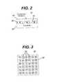
- FIG. 2is a side cross-sectional view of an array of organic light emitting diodes containing a light scattering medium according to a preferred embodiment of the present invention.
- FIGS. 3-6are top views of arrays of organic light emitting diodes according to preferred embodiments of the present invention.
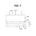
- FIG. 7is a side cross-sectional view of an organic light emitting diode according to one preferred embodiment of the invention.
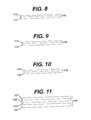
- FIGS. 8-11illustrate various examples of organic light emitting layers formed of two or more sublayers.
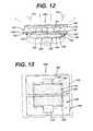
- FIG. 12is a side cross-sectional view of an organic light emitting diode according to another preferred embodiment of the invention.
- FIG. 13is a bottom view of the organic light emitting diode of FIG. 12 .
- FIG. 14illustrates a method of making the organic light emitting diode of FIG. 12 according to a preferred embodiment of the present invention.
- FIG. 15illustrates a method of mounting a plurality of light emitting devices on a mounting substrate to produce a light emitting device according to a preferred embodiment of the invention.
- a light emitting devicecontains a layer of scattering media above the light emitting surface of the array. The function of this scattering media is to facilitate mixing between the light emitted from the separate OLED devices.
- the present inventorhas also realized that it is desirable for a light emitting device to have a color tunable light output for general lighting applications, such as mood lighting for home or industry, or spotlights for theaters and discos.
- the light emitting devicemay be controlled by a user or by a computer to generate a desired color of the light emitted by the device.
- various sets of plurality of OLEDs in the arrayare separately electrically connected so that they can be controlled in tandem by a power controller.
- a desired color of lightis obtained by adjusting the power provided to the separate sets of OLEDs in the array.
- FIG. 2A side view of a light emitting device 21 containing the OLED array according to a first preferred embodiment is illustrated in FIG. 2 .
- the horizontal arraycontains OLED devices 23 , emitting light of different colors, formed over a substrate 25 .
- the term lightmay include UV and IR radiation in addition to visible light of different colors (i.e., of different wavelength or color temperature).
- the arraycontains OLEDs emitting red, green and blue light (indicated by the letters R, G and B in the Figures).
- the light emitting surface of the arrayi.e., the top surface in FIG. 2
- the scattering layer 27is placed on top of the OLEDs 23 , and if desired, also in the interstitial areas between the OLEDs.
- the scattering mediamay comprise small particles with relatively high index of refraction that do not appreciably absorb the visible light from the OLED devices.
- the light scattering particlesmay have a mean particles size of 50 to 500 nm.
- the mean particle sizeis between ⁇ /3 and ⁇ /2, where ⁇ is the peak emission wavelength of the OLEDs 23 .
- the preferred light scattering particlesare titania, alumina, or zinc oxide particles, such as the Dupont R960 TiO 2 particles coated with an alumino-silicate glass having a mean particle size of 300 nanometers.
- BaTiO 3 , SiO 2 , CaCO 3 , BaSO 4 and diamond light scattering particlesmay also be used.
- the scattering layer 27may comprise a layer of packed light scattering particles or a carrier medium containing the light scattering particles.
- the carrier mediummay be glass or a polymer materials, such as epoxy, silicone or urea resin. However, other carrier medium and scattering particle materials may be used, if desired.
- FIG. 3illustrates a top view of a white light emitting device 31 which includes the OLED 33 array tiled onto the substrate 35 .
- the OLED devicesemit light of three different colors, such as red, green and blue, which when mixed in different ratios provides different colors of white light (i.e., a white light having different color temperatures). However, other combinations of primary and/or mixed colors, such as a combination of blue and yellow light, may be used to produce white light.
- the array of OLEDs 33is depicted as a regular array of alternating red, green and blue OLEDs in a square pattern.
- the OLEDsmay be formed in an irregular array or pattern.
- the different color OLEDsmay have different shapes and areas, if desired.
- the different OLEDs 33can be fabricated together on the device substrate 35 using patterning techniques such as shadow-masking, ink-jet printing or screen printing. Alternatively, the different OLED 33 can be fabricated separately and then physically attached onto the substrate 35 .
- the OLED array of the light emitting deviceincludes a first set of plurality of OLEDs electrically connected together to the same power source such that each OLED receives the same power signal at the same time.
- the first set of OLEDsemit light of a first color.
- the OLED arrayalso includes a second set of plurality of OLEDs electrically connected together to the same power source such that each OLED receives the same power signal at the same time.
- the second set of OLEDsemit light of a second color different than the first color.
- the term “same power source”includes a single power source which provides a different amount of power to the first and second sets of OLEDs, as well as plural power sources, each of which provides the same amount of power to each OLED of one OLED set.
- the light emitting devicealso includes a power controller which provides a first amount of power to the first set of OLEDs and a second amount of power to the second set of OLEDs to obtain a device light output having a desired color.
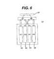
- FIGS. 4-6each illustrate a top view of a light emitting device according to the second through fourth preferred embodiments, respectively, which illustrate the above concept.
- the devices of the second through fourth embodimentscontain the scattering media of the first embodiment.
- the scattering mediamay be omitted to simplify device processing.
- FIG. 4illustrates a light emitting device 41 according to the second preferred embodiment.
- the device 41includes an integrated controller 42 , such as a microprocessor or an ASIC chip.
- the controllermay comprise a computer located remotely from the light emitting device, or a wall switch or dial which is actuated by the user.
- the first set 44 of OLEDs 43comprises a plurality of red light emitting OLEDs and the second set 45 of OLEDs comprises a plurality of green light emitting OLEDs.
- the devicealso includes a third set 46 of a plurality of blue light emitting OLEDs 43 electrically connected together to the same power source such that each OLED receives the same power signal at the same time.
- all the OLEDs 44 which emit red lightcan be connected together, all the OLEDs 45 which emit green light can be connected together, and all the OLEDs 46 which emit blue light can be connected together, as illustrated in FIG. 4 . In this manner, all colors from the pure red, green and blue to the various mixed whites can be obtained.
- Each of the first, second and third sets of OLEDs 44 , 45 , 46are connected in parallel to their respective power source 47 , 48 , 49 . While not as preferred, the OLEDs alternatively may be connected to their respective power sources in series.
- the power sources 47 , 48 and 49may comprise driver circuits or switches connected to an outside voltage source, such as a power outlet or battery.
- the separate power sources 47 , 48 and 49may alternatively comprise a single driver circuit which is capable of simultaneously providing a different power signal to each OLED set.
- the device 41operates as follows.
- the controller 42actuates the first power source 47 to provide a first power signal having a first magnitude to a first set of plurality of OLEDs 44 . such that the first set of OLEDs 44 emits red light of a first color.
- the controller 42actuates the second power source 48 to provide a second power signal having a second magnitude to a second set of plurality of OLEDs 45 , such that the second set of OLEDs emits green light.
- the controller 42also actuates the third power source 49 to provide a third power signal having a third magnitude to a third set of plurality of OLEDs 46 , such that the third set of OLEDs emits blue light.
- the tuned red, green and red lightappears as white light of a desired color and color temperature to a human observer.
- FIG. 5illustrates a light emitting device 51 according to the third preferred embodiment.
- the OLED array in device 51comprises a first set of OLEDs 54 which contains a plurality of red, green and blue light emitting OLEDs 53 .
- the arrayalso contains a second set of OLEDs 55 which contains second set of a plurality of red, green and blue light emitting OLEDs 53 .
- the red, green and blue light emission from the first set of OLEDs 54appears as a first white color light
- the red, green and blue light emission from the second set of OLEDs 55appears as a second white color light different from the first white color light.
- the white light emitted from the first set of OLEDs 54has a first color temperature
- the white light emitted from the second set of OLEDs 54has a different, second color temperatures. Then by separately controlling the power from the respective power sources 57 , 58 to these two sets OLEDs by using the controller 52 , white light having any color or color temperature value between respective values of color or color temperature of the white light emitted by the two sets of OLEDs 54 , 55 can be obtained.
- FIG. 6depicts a white light emitted device 61 according to the fourth preferred embodiment of the present invention.
- a plurality of OLEDsare placed in the array.
- the arraycomprises two different types of white light emitting OLEDs.
- the first type of OLEDs 64emit white light having a first color temperature (labeled “W 1 ” in FIG. 6 ).
- the second type of OLEDs 65emit white light having a second color temperature (labeled “W 2 ” in FIG. 6 ) different from the first temperature.
- the first set of white light emitting OLEDs 64 which emit white light having the same first color temperatureare electrically connected together to the same power source 67 .
- the second set of white light emitting OLEDs 65 which emit white light having the same second color temperatureare electrically connected together to the same power source 68 , but separately from the first OLEDs 64 .
- the white light emitting OLEDscan be made for instance using a blue light emitting OLED device covered with a downshifting phosphor, such as the phosphor described in U.S. Application Ser. No. 60/178,451, incorporated by reference in its entirety.
- the phosphorcomprises an ADE:Ce 3+ phosphor, where A comprises at least one of Y or Gd, D comprises at least one of Al, Ga or Sc and E comprises oxygen.
- This phosphoremits yellow light, such that the combined blue and yellow emission from the OLEDs appears as white light to a human observer.
- a specific example of such a phosphoris Y 3 Al 5 O 12 :Ce 3+ (commonly known as YAG:Ce 3+ ).
- the preferred organic blue light emitting polymer layer in an OLEDis poly(9,9-di-n-hexylfluorene-2,7-diyl). However, other phosphors and organic light emitting materials may be suitable in these applications.
- the OLEDpreferably also contains a transparent ITO anode and a LiF/Al bilayer cathode.
- the different color temperaturescan be obtained by using different phosphors with the same blue OLED device.
- the ADE:Ce 3+ phosphor yellow emissionshifts to longer wavelengths.
- the combination of the blue OLED light and the longer wavelength yellow light emitted by such phosphorappears as white light having a lower color temperature, such as a color temperature of about 2500K to about 5000K.
- the ADE:Ce 3+ phosphor yellow emissionshifts to shorter wavelengths.
- the combination of the blue OLED light and the shorter wavelength yellow light emitted by such phosphorappears as white light having a higher color temperature, such as a color temperature of about 5000K to about 8500K. Therefore, by varying the power to OLEDs 64 , 65 , a device 61 white light output having a color temperature between 2500K and 8500K can be obtained.
- each OLEDis connected to two row or two column electrodes, to allow for common control of a plurality of OLEDs.
- each subpixel 3 in FIG. 1is connected to one row and one column electrode to allow for independent subpixel control.
- the OLED described abovemay comprise any type of organic light emitting diode or device.
- the term “light”includes visible light as well as UV and IR radiation.
- the device 100according to one preferred aspect of the present invention is illustrated in FIG. 7 .
- the device 100includes an organic light emitting layer 110 disposed between two electrodes, e.g., a cathode 120 and an anode 130 .
- the organic light emitting layer 110emits light upon application of a voltage across the anode and cathode from the voltage source “V”.
- the organic light emitting device 100typically includes a device substrate 125 , such as glass or transparent plastics such as PET (MYLAR®), polycarbonate, and the like, as shown in FIG. 7 .
- organic light emitting devicegenerally refers to the combination which includes the organic light emitting layer, the cathode, and the anode, and which may also include other elements such as the device substrate, device electrical contacts, and a photoluminescent layer, as will be described below.
- the anode and cathodeinject charge carriers, i.e., holes and electrons, into the organic light emitting layer 110 where they recombine to form excited molecules or excitons which emit light when the molecules or excitons decay.
- the color of light emitted by the moleculesdepends on the energy difference between the excited state and the ground state of the molecules or excitons.
- the applied voltageis about 3-10 volts but can be up to 30 volts or more, and the external quantum efficiency (photons out/electrons in) is between 0.01% and 5%, but could be up to 10%, 20%, 30%, or more.
- the organic light emitting layer 110typically has a thickness of about 50-500 nanometers, and the electrodes 120 , 130 each typically have a thickness of about 100-1000 nanometers.
- the cathode 120generally comprises a material having a low work function value such that a relatively small voltage causes emission of electrons from the cathode.
- the cathode 120may comprise, for example, calcium or a metal such as gold, indium, manganese, tin, lead, aluminum, silver, magnesium, or a magnesium/silver alloy.
- the cathodecan be made of two layers to enhance electron injection. Examples include a thin inner layer of LiF followed by a thicker outer layer of aluminum or silver, or a thin inner layer of calcium followed by a thicker outer layer of aluminum or silver.
- the anode 130typically comprises a material having a high work function value.
- the anode 130is preferably transparent so that light generated in the organic light emitting layer 110 can propagate out of the organic light emitting device 100 .
- the anode 130may comprise, for example, indium tin oxide (ITO), tin oxide, nickel, or gold.
- ITOindium tin oxide
- the electrodes 120 , 130can be formed by conventional vapor deposition techniques, such as evaporation or sputtering, for example.
- the organic light emitting layer 110comprises a single layer.
- the organic light emitting layer 110may comprise, for example, a conjugated polymer which is luminescent, a hole-transporting polymer doped with electron transport molecules and a luminescent material, or an inert polymer doped with hole transporting molecules and a luminescent material.
- the organic light emitting layer 110may also comprise an amorphous film of luminescent small organic molecules which can be doped with other luminescent molecules.
- the organic light emitting layer 110comprises two or more sublayers which carry out the functions of hole injection, hole transport, electron injection, electron transport, and luminescence. Only the luminescent layer is required for a functioning device. However, the additional sublayers generally increase the efficiency with which holes and electrons recombine to produce light.
- the organic light emitting layer 110can comprise 1-4 sublayers including, for example, a hole injection sublayer, a hole transport sublayer, a luminescent sublayer, and an electron injection sublayer.
- one or more sublayersmay comprise a material which achieves two or more functions such as hole injection, hole transport, electron injection, electron transport, and luminescence.
- the organic light emitting layer 110comprises a conjugated polymer.
- conjugated polymerrefers to a polymer which includes a delocalized ⁇ -electron system along the backbone of the polymer.
- the delocalized ⁇ -electron systemprovides semiconducting properties to the polymer and gives it the ability to support positive and negative charge carriers with high mobilities along the polymer chain.
- the polymer filmhas a sufficiently low concentration of extrinsic charge carriers that on applying an electric field between the electrodes, charge carriers are injected into the polymer and radiation is emitted from the polymer. Conjugated polymers are discussed, for example, in R. H. Friend, 4 Journal of Molecular Electronics 37-46 (1988).
- PPVpoly(p-phenylenevinylene)
- PPVpoly(p-phenylenevinylene)
- a suitable PPV filmtypically has a thickness of about 100-1000 nanometers.
- the PPV filmcan be formed by spin coating a solution of the precursor to PPV in methanol onto a substrate and heating in a vacuum oven.
- the phenylene ring of the PPVcan optionally carry one or more substituents each independently selected from alkyl, alkoxy, halogen, or nitro.
- Other conjugated polymers derived from PPVmay also be used in conjunction with exemplary embodiments of the invention. Examples of such derivatives of PPV include: 1) polymers derived by replacing the phenylene ring with a fused ring system, e.g. replacing the phenylene ring with an anthracene or napthalene ring system.
- These alternative ring systemsmay also carry one or more substituents of the type described above with respect to the phenylene ring; 2) polymers derived by replacing the phenylene ring with a heterocyclic ring system such as a furan ring.
- the furan ringmay carry one or more substituents of the type described above in connection with the phenylene ring; 3) polymers derived by increasing the number of vinylene moieties associated with each phenylene or other ring system.
- the above described derivativeshave different energy gaps, which allows flexibility in producing an organic light emitting layer 110 which emits in a desired color range or ranges. Additional information on luminescent conjugated polymers is described in U.S. Pat. No. 5,247,190, which is hereby incorporated by reference.
- Suitable conjugated polymersinclude polyfluorenes such as 2,7-substituted-9-substituted fluorenes and 9-substituted fluorene oligomers and polymers.
- Polyfluorenesgenerally have good thermal and chemical stability and high solid-state fluorescence quantum yields.
- the fluorenes, oligomers and polymersmay be substituted at the 9-position with two hydrocarbyl moieties which may optionally contain one or more of sulfur, nitrogen, oxygen, phosphorous or silicon heteroatoms; a C 5-20 ring structure formed with the 9-carbon on the fluorene ring or a C 4-20 ring structure formed with the 9-carbon containing one or more heteroatoms of sulfur, nitrogen or oxygen; or a hydrocarbylidene moiety.
- the fluorenesare substituted at the 2- and 7-positions with aryl moieties which may further be substituted with moieties which are capable of crosslinking or chain extension or a trialkylsiloxy moiety.
- the fluorene polymers and oligomersmay be substituted at the 2- and 7-positions.
- the monomer units of the fluorene oligomers and polymersare bound to one another at the 2- and 7′-positions.
- the 2,7′-aryl-9-substituted fluorene oligomers and polymersmay be further reacted with one another to form higher molecular weight polymers by causing the optional moieties on the terminal 2,7′-aryl moieties, which are capable of crosslinking or chain extension, to undergo chain extension or crosslinking.
- fluorenes and fluorene oligomers or polymersare readily soluble in common organic solvents. They are processable into thin films or coatings by conventional techniques such as spin coating, spray coating, dip coating and roller coating. Upon curing, such films demonstrate resistance to common organic solvents and high heat resistance. Additional information on such polyfluorenes is described in U.S. Pat. No. 5,708,130, which is hereby incorporated by reference.
- poly(fluorene) copolymerssuch as poly(fluorene-co-anthracene)s, which exhibit blue electroluminescence.
- These copolymersinclude a polyfluorene subunit such as 2,7-dibromo-9,9-di-n-hexylfluorene (DHF) and another subunit such as 9,10-dibromoanthracene (ANT).
- DHF2,7-dibromo-9,9-di-n-hexylfluorene
- ANT9,10-dibromoanthracene
- High molecular weight copolymers from DHF and ANTcan be prepared by the nickel-mediated copolymerization of the corresponding aryl dibromides.
- the final polymer molecular weightcan be controlled by adding the end capping reagent 2-bromofluorene at different stages of the polymerization.
- the copolymersare thermally stable with decomposition temperatures above 400° C. and are soluble in common organic solvents such as tetrahydrofuran (THF), chloroform, xylene, or chlorobenzene. They emit blue light having a wavelength of about 455 nm. Additional information on such polyfluorenes is described in Gerrit Klarner et al., “Colorfast Blue Light Emitting Random Copolymers Derived from Di-n-hexylfluorene and Anthracene”, 10 Adv. Mater.
- Another preferred blue light emitting polyfluorineis poly(9,9-di-n-hexylfluorine-2,7-diyl) which has a broad double emission peak between about 415 and 460 nm.
- the organic light emitting layer 110comprises a molecularly doped polymer.
- a molecularly doped polymertypically comprises a binary solid solution of charge transporting molecules which are molecularly dispersed in an inert polymeric binder.
- the charge transporting moleculesenhance the ability of holes and electrons to travel through the doped polymer and recombine.
- the inert polymeroffers many alternatives in terms of available dopant materials and mechanical properties of the host polymer binder.
- a molecularly doped polymercomprises poly(methyl methacrylate) (PMMA) molecularly doped with the hole transporting molecule N,N′-diphenyl-N,N′-bis(3-methylsphenyl)-1,1′-biphenyl-4,4′-diamine (TPD) and the luminescent material tris(8-quinolinolato)-aluminum(IR) (Alq).
- TDPhas a high hole drift mobility of 10 ⁇ 3 cm 2 /volt-sec, while Alq is a luminescent metal complex having electron transporting properties in addition to its luminescent properties.
- the doping concentrationis typically about 50%, while the molar ratio of TDP to Alq may vary from about 0.4 to 1.0, for example.
- a film of the doped PMMAcan be prepared by mixing a dichloroethane solution containing suitable amounts of TPD, Alq, and PMMA, and dip coating the solution onto the desired substrate, e.g. an indium tin oxide (ITO) electrode.
- the thickness of the doped PMMA layeris typically about 100 nanometers.
- ITOindium tin oxide
- a green emissionis generated. Additional information on such doped polymers is described in Junji Kido et al., “Organic Electroluminescent Devices Based on Molecularly Doped Polymers”, 61 Appl. Phys. Lett. 761-763 (1992), which is hereby incorporated by reference.
- the organic light emitting layer 110comprises two sublayers.
- the first sublayer 111provides hole transport, electron transport, and luminescent properties and is positioned adjacent the cathode 120 .
- the second sublayer 112serves as a hole injection sublayer and is positioned adjacent the anode 130 .
- the first sublayer 111comprises a hole-transporting polymer doped with electron transporting molecules and a luminescent material, e.g. a dye or polymer.
- the hole-transporting polymermay comprise poly(N-vinylcarbazole) (PVK), for example.
- the electron transport moleculesmay comprise 2-(4-biphenyl)-5-(4-tert-butylphenyl)-1,3,4-oxadiazole (PBD), for example.
- the luminescent materialtypically comprises small molecules or polymers which act as emitting centers to vary the emission color.
- the luminescent materialsmay comprise the organic dyes coumarin 460 (blue), coumarin 6 (green) or nile red.
- Thin films of these blendscan be formed by spin coating a chloroform solution containing different amounts of PVK, electron transport molecules, and luminescent materials.
- a suitable mixturecomprises 100 weight percent PVK, 40 weight percent PBD, and 0.2-1.0 weight percent organic dye.
- the second sublayer 112serves as a hole injection sublayer and may comprise poly(3,4)ethylenedioxythiophene/polystyrenesulphonate (PEDT/PSS), for example, available from Bayer Corporation, which can be applied by conventional methods such as spin coating. Additional information on hole-transporting polymers doped with electron transporting molecules and a luminescent material is described in Chung-Chih Wu et al., “Efficient Organic Electroluminescent Devices Using Single-Layer Doped Polymer Thin Films with Bipolar Carrier Transport Abilities”, 44 IEEE Trans. on Elec. Devices 1269-1281 (1997), which is hereby incorporated by reference.
- PDT/PSSpoly(3,4)ethylenedioxythiophene/polystyrenesulphonate
- the organic light emitting layer 110includes a first sublayer 113 comprising a luminescent sublayer and a second sublayer 114 comprising a hole transporting sublayer.
- the hole transporting sublayer 114may comprise an aromatic amine that is readily and reversibly oxidizable, for example.
- a luminescent sublayer and a hole transporting sublayeris described in A. W. Grice et al, “High Brightness and Efficiency of Blue Light-Emitting Polymer Diodes”, 73 Appl. Phys. Letters 629-631 (1998), which is hereby incorporated by reference.
- the device described thereincomprises two polymer layers sandwiched between an ITO electrode and a calcium electrode.
- the polymer layer next to the ITOis a hole transport layer and comprises a polymeric triphenyldiamine derivative (poly-TPD).
- the blue emitting polymer layer which is next to the calcium electrodeis poly(9,9-dioctylfluorene).
- the organic light emitting layer 110comprises a first sublayer 115 which includes luminescent and hole transport properties, and a second sublayer 116 which includes electron injection properties.
- the first sublayer 115comprises a polysilane, and the second sublayer comprises an oxadiazole compound. This structure produces ultraviolet (UV) light.
- Polysilanesare linear silicon (Si)-backbone polymers substituted with a variety of alkyl and/or aryl side groups. In contrast to ⁇ -conjugated polymers, polysilanes are quasi one-dimensional materials with delocalized ⁇ -conjugated electrons along the polymer backbone chain. Due to their one-dimensional direct-gap nature, polysilanes exhibit a sharp photoluminescence with a high quantum efficiency in the ultraviolet region.
- polysilanesexamples include poly(di-n-butylsilane) (PDBS), poly(di-n-pentylsilane) (PDPS), poly(di-n-hexylsilane) (PDHS), poly(methyl-phenylsilane) (PMPS), and poly[-bis(p-butylphenyl)silane] (PBPS).
- the polysilane sublayer 115can be applied by spin coating from a toluene solution, for example.
- the electron injection sublayer 116may comprise 2,5-bis(4-biphenyl)-1,3,4-oxadiazole (BBD), for example.
- BBD2,5-bis(4-biphenyl)-1,3,4-oxadiazole
- UV-emitting polysilane organic light emitting layersAdditional information on UV-emitting polysilane organic light emitting layers is described in Hiroyuki Suzuki et al, “Near-ultraviolet Electroluminescence from Polysilanes”, 331 Thin Solid Films 64-70 (1998), which is hereby incorporated by reference.
- the organic light emitting layer 110comprises a hole injecting sublayer 117 , a hole transporting sublayer 118 , a luminescent sublayer 119 , and an electron injecting sublayer 121 .
- the hole injecting sublayer 117 and hole transporting sublayer 118efficiently provide holes to the recombination area.
- the electrode injecting sublayer 121efficiently provides electrons to the recombination area.
- the hole injecting sublayer 117may comprise a porphyrinic compound, such as a metal free phthalocyanine or a metal containing phthalocyanine, for example.
- the hole transporting sublayer 118may comprise a hole transporting aromatic tertiary amine, where the latter is a compound containing at least one trivalent nitrogen atom that is bonded only to carbon atoms, at least one of which is a member of an aromatic ring.
- the luminescent sublayer 119may comprise, for example, a mixed ligand aluminum chelate emitting in the blue wavelengths, such as bis(R-8-quinolinolato)-(phenolato)aluminum(III) chelate where R is a ring substituent of the 8-quinolinolato ring nucleus chosen to block the attachment of more than two 8-quinolinolato ligands to the aluminum atom.
- the electron injection sublayer 121may comprise a metal oxinoid charge accepting compound such as a tris-chelate of aluminum. Additional information on such four-layer materials and devices are described in U.S. Pat. No. 5,294,870, which is hereby incorporated by reference.
- organic light emitting layers 110can be used to design an organic light emitting device which emits in one or more desired colors.
- the organic light emitting device 100can emit ultraviolet, blue, green, or red light.
- the organic light emitting device 200may optionally include a photoluminescent layer 135 .
- the photoluminescent layer 135comprises a photoluminescent material which absorbs light from the organic light emitting layer 110 and emits light typically having a longer wavelength.
- the photoluminescent materialpreferably comprises an inorganic phosphor, such as YAG:Ce 3+ , but may also comprise an organic photoluminescent material such as an organic dye.
- the organic light emitting device 200comprises an organic light emitting layer 110 , a cathode 120 , and an anode 130 which is light transmissive.
- the organic light emitting device 200also includes a device substrate 125 which is light transmissive.
- the elements in FIGS. 12 and 13e.g. the anode 130 , cathode 120 , light emitting layer 110 ) corresponding to those in FIG. 7 can be formed of the same materials as described above with respect to FIG. 7 .
- lightrepresented by arrows 101
- lightis generated in the light emitting layer 110 and propagates through the anode 130 and the device substrate 125 .
- a sealing member 150Adjacent to the cathode 120 is a sealing member 150 , typically comprising glass, which provides a barrier to oxygen and water.
- the sealing member 150in conjunction with a sealant 152 which may comprise epoxy, a metal, or a glass frit, for example, provides a near hermetic barrier to prevent water and oxygen penetration into the cathode 120 , anode 130 and organic light emitting layer 110 .
- first and second device electrical contacts 162 , 164are Formed adjacent to the sealing member 150 , which provide electrical connections to the anode 130 and cathode 120 , respectively.
- the first device electrical contact 162connects electrically to the anode 130 in a tab region 132 of the anode 130 .
- the tab region 132is beyond the perimeter of the sealing member 150 .
- the second device electrical contact 164connects electrically to the cathode 120 in a tab region 124 of the cathode 120 .
- the tab region 124is beyond the perimeter of the sealing member 150 .
- the organic light emitting layer 110typically occupies at least the overlap region of the anode 130 and cathode 120 and may extend beyond these electrodes.
- the device electrical contacts 162 , 164typically have respective device contacting surfaces 163 , 165 which occupy a common plane. These device contacting surfaces 163 , 165 facilitate the mounting of one or more organic light emitting devices 200 onto a mounting substrate, as will be described further below in connection with FIG. 12 .
- the imaginary surfacewhich is typically planar, divides the organic light emitting device 200 into a first side and a second side.
- the anode 130is on the first side
- the cathode 120is on the second side.
- the lightis emitted through the first side
- the device electrical contacts 162 , 164extend to the second side.
- the first device electrical contact 162extends from the anode 130 on the first side to the second side of the organic light emitting device.
- the second device electrical contact 164extends from the cathode 120 on the second side to another location on the second side of the organic light emitting device.
- the organic light emitting device 200can be powered by contacting both device electrical contacts 162 , 164 on a common planar surface 163 , 165 which is on an opposite side of the organic light emitting device as where the light emission occurs.
- the planar surface defined by surfaces 163 , 165is parallel to the light emitting layer 110 and the device substrate 125 . This configuration allows a number of organic light emitting devices 200 to be easily mounted adjacent to each other (“tiled”) on a mounting substrate.
- the device substrate 125can define the area of the organic light emitting device 200 .
- the first and second device electrical contacts 162 , 164can occupy an area which is within the area of the device substrate 125 . Therefore, two organic light emitting devices 200 can be placed directly adjacent to each other without any electrical connectors in between and with a small separation distance between the adjacent light emitting device substrates 125 .
- the separation distancecould be less than 2 centimeters (cm), 1 cm, 0.5 cm or 0.25 cm, but is typically greater than 0.1 cm.
- the organic light emitting device 200also includes the layer of light scattering media 145 comprising light scattering particles for effective color mixing, as described above.
- the scattering layer 145is preferably formed over the top and sides of each organic light emitting device. However, if desired, the scattering layer may be formed only over the top of each device 200 , as illustrated in FIG. 12 .
- an optional shaped transparent materialis formed onto the emitting surface of the device to improve the device quantum efficiency.
- the transparent materialcan be any transparent polymer or glass, for example, and can be filled with high index nanoparticles such that its index of refraction matches that of the device. This reduces the Fresnel loss in the external quantum efficiency of the device.
- the transparent materialis shaped such that its top, light emitting, surface has dimples or corrugations which reduce the amount of light lost through total internal reflection. This reduces the critical angle loss in the external quantum efficiency of the device.
- the shaped materialmay be an additional layer attached to the light emitting surface of the device substrate 125 .
- the shaped materialmay comprise the device substrate 125 .
- the shaped transparent materialtypically has an index of refraction which is matched to or close to the index of refraction of the substrate or the active layer of the OLED device 100 .
- the shape of the material to be attachedis flat on the side of attachment and dimpled or corrugated, for example, on the side from which light is emitted into the ambient environment.
- the height of the corrugations or dimplesis typically greater than 0.1 micron and typically covers the whole surface.
- the spacing between dimple or corrugation peaksis typically within a factor of 10 of their height. The spacing does not have to conform to a regular pattern.
- the shaped transparent materialcan be made with any thermoplastic, thermoset, or elastomer material that is transparent and can be molded into the desired structure.
- the index of refraction of the materialcan be adjusted to match that of the surface of the device 100 by the mixing of high index of refraction nanoparticles, such as TiO 2 or ZnO, into a base polymer or glass material, such as epoxy. In this manner, the index of the resulting composite can be adjusted between the values of the pure base and the pure filler.
- the size of the nanoparticlesis less than 100 nanometers to eliminate scattering effects and ensure transparency.
- the shaped materialcan be attached to the light emitting surface of the device 100 by means of a transparent adhesive, such as an epoxy. It is typically desirable that the epoxy have close to the same index of refraction as that of the device 100 surface. This can be achieved by filling the epoxy with a specific amount of nanoparticle.
- the layer of scattering media 145 and the index matched materialcomprise the same layer.
- the nanoparticles having a size less than 100 nanometersare mixed into the to layer of scattering media 145 to adjust the index of refraction of the layer 145 such that it is equal to or close to the index of refraction of the device substrate 125 .
- the layer of scattering media 145may also have a dimpled light emitting surface in order to reduce the critical angle loss at the light emitting surface of the layer 145 .
- FIG. 14illustrates a method for forming the organic light emitting device 200 of FIGS. 12 and 13 according to an exemplary embodiment of the invention.
- a glass substrate 125is sputter coated with a layer of thin indium tin oxide (ITO).
- ITOis then patterned to form the anode 130 , e.g. in the pattern shown in FIG. 13 .
- the organic light emitting layer 110(which may include one or more sublayers as shown in FIGS. 7-11 ) is deposited, for example by spin coating or inkjet processing.
- the cathode 120is deposited as a reflective structure comprising a thin layer of lithium fluoride overcoated with aluminum, for example.
- the cathode 120can be deposited through a stencil mask by evaporation, for example.
- the sealing member 150which may comprise glass, for example, is next applied with a sealant 152 in step 4 to form a near hermetic barrier.
- step 5the organic light emitting layer 110 extending beyond the sealing member 150 is removed by solvent or dry etching methods.
- the device electrical contacts 162 , 164which may comprise a metal such as aluminum or silver, are then applied to the reflective side of the organic light emitting device 200 in step 6 .
- the device electrical contacts 162 , 164allow for external contact to the organic light emitting device and additionally can provide a near hermetic seal to the anode 130 , cathode 120 , and light emitting layer 110 .
- step 7optionally, a layer 135 of photoluminescent material, e.g. an inorganic phosphor, is applied to the device substrate 125 .
- a layer of scattering particlescan be applied in a subsequent step.
- the steps shown in FIG. 14are of course merely an example of a method of making a light source, and not intended to be limiting.
- FIG. 15illustrates a method of mounting one or more organic light emitting devices onto a mounting substrate to form a light emitting device according to an exemplary embodiment of the invention.
- Step 1shows the mounting substrate 160 , which may comprise a conventional printed circuit board such as FR4 or GETEK, or a flexible polymer film such as Kapton ETM or Kapton HTM polyimide (Kapton is a trademark of E. I. Du Pont de Nemours & Co.), Apical AV polyimide (Apical is a trademark of Kanegafugi Chemical Company), or Upilex polyimide (Upilex is a trademark of UBE Industries, Ltd) for example.
- free-standing KaptonTM polyimideis mounted on a rigid frame (not shown in FIG.
- An adhesivetypically comprising a material capable of adhering at a low temperature, can be applied to the rigid frame.
- suitable adhesivesinclude materials such as ULTEM polyetherimide (ULTEMTM is a trademark of General Electric Company) and MULTIPOSITTM XP-9500 thermoset epoxy (MULTIPOSIT is a trademark of Shipley Company Inc., Marlborough, Mass.).
- step 2another adhesive 161 , which is typically organic, such as ULTEMTM, SPIE (siloxane polyimide epoxy) or other polyimide and epoxy blends, or cyanoacrylate is applied to the mounting substrate 160 , as shown in FIG. 15 .
- step 3one or more organic light emitting devices 200 are placed on the adhesive 161 , and the adhesive is cured to bond the organic light emitting devices 200 to the mounting substrate 160 .
- vias 169are formed using laser ablation or reactive ion etching, for example, through the mounting substrate 160 and the adhesive 161 to the device contacting surfaces 163 , 165 of the device electrical contacts 162 , 164 , respectively.
- first and second mounting electrical contacts 172 , 174are formed or inserted into the via holes 169 to make contact with the device electrical contacts 162 , 164 , respectively.
- the mounting electrical contacts 172 , 174can be formed as a patterned metal layer using sputter or electroless plating techniques, in combination with electroplating if desired, and patterned with a standard photoresist and etch process.
- the interconnect metallizationin one embodiment comprises a thin adhesion layer of 1000 angstroms ( ⁇ ) sputtered titanium, coated by a thin layer of 3000 ⁇ sputtered copper, coated by a layer of electroplated copper to a thickness of 4 microns, for example.
- An optional buffer layer of 1000 ⁇ of titaniumcan be applied over the electroplated copper.
- the mounting electrical contacts 172 , 174can also be applied by the conventional methods of evaporation with a shadow mask or screen printing.
- the scattering layer 145can be applied to organic light emitting devices 200 individually, or more typically can be applied across a number of organic light emitting devices 200 , as shown in FIG. 15 .
- a nonconductive materialsuch as SPIE (siloxane polyimide epoxy) can be inserted into the gaps 175 between adjacent organic light emitting devices 200 .
- a large area light emitting devicesuch as a 2 ft. by 2 ft. device, may be formed by attaching a plurality of individual OLEDs 200 to a mounting substrate 160 using the method described above or other mounting methods.
- Thisis advantageous in forming a large area light emitting device because the device is not limited by the size of the substrate used to make each OLED, in contrast to the display device of the '551 patent in which all the OLEDs are fabricated on the same glass substrate.
- the size of the display device of the '551 patentis limited by the size of the glass substrate. While mounting of prefabricated OLEDs to the mounting substrate, as illustrated in FIG. 15 is preferred, in an alternative aspect of the present invention, all OLEDs of the light emitting device may be directly fabricated on the same substrate.
- embodiments of the present inventionallow the organic light emitting devices 200 to be placed very close to each other on the mounting substrate 160 , it may be desirable in some applications to have a larger spacing between individual organic light emitting devices 200 . In such cases, it is desirable to also place the scattering layer between organic light emitting devices 200 .
- the mounting substrate 160is designed to be flexible, curved, or non-planar.
- the mounting substrate 160may be formed in any desired shape, e.g. to conform to an existing building structure. After the mounting electrical contacts have been installed, they can be connected to a suitable power supply, as illustrated in FIGS. 3-5 , for example.
Landscapes
- Physics & Mathematics (AREA)
- Optics & Photonics (AREA)
- Electroluminescent Light Sources (AREA)
Abstract
Description
Claims (4)
Priority Applications (1)
| Application Number | Priority Date | Filing Date | Title |
|---|---|---|---|
| US10/666,145US6841949B2 (en) | 2000-03-31 | 2003-09-22 | Color tunable organic electroluminescent light source |
Applications Claiming Priority (3)
| Application Number | Priority Date | Filing Date | Title |
|---|---|---|---|
| US19406800P | 2000-03-31 | 2000-03-31 | |
| US09/684,483US6661029B1 (en) | 2000-03-31 | 2000-10-10 | Color tunable organic electroluminescent light source |
| US10/666,145US6841949B2 (en) | 2000-03-31 | 2003-09-22 | Color tunable organic electroluminescent light source |
Related Parent Applications (1)
| Application Number | Title | Priority Date | Filing Date |
|---|---|---|---|
| US09/684,483DivisionUS6661029B1 (en) | 2000-03-31 | 2000-10-10 | Color tunable organic electroluminescent light source |
Publications (2)
| Publication Number | Publication Date |
|---|---|
| US20040061107A1 US20040061107A1 (en) | 2004-04-01 |
| US6841949B2true US6841949B2 (en) | 2005-01-11 |
Family
ID=29714787
Family Applications (2)
| Application Number | Title | Priority Date | Filing Date |
|---|---|---|---|
| US09/684,483Expired - LifetimeUS6661029B1 (en) | 2000-03-31 | 2000-10-10 | Color tunable organic electroluminescent light source |
| US10/666,145Expired - LifetimeUS6841949B2 (en) | 2000-03-31 | 2003-09-22 | Color tunable organic electroluminescent light source |
Family Applications Before (1)
| Application Number | Title | Priority Date | Filing Date |
|---|---|---|---|
| US09/684,483Expired - LifetimeUS6661029B1 (en) | 2000-03-31 | 2000-10-10 | Color tunable organic electroluminescent light source |
Country Status (1)
| Country | Link |
|---|---|
| US (2) | US6661029B1 (en) |
Cited By (25)
| Publication number | Priority date | Publication date | Assignee | Title |
|---|---|---|---|---|
| US20040032205A1 (en)* | 2002-08-16 | 2004-02-19 | Michael Hack | Organic light emitting devices for illumination |
| US20050147743A1 (en)* | 2002-03-13 | 2005-07-07 | Takuro Sekiya | Fabrication of functional device mounting board making use of inkjet technique |
| US20050248935A1 (en)* | 2004-05-04 | 2005-11-10 | Eastman Kodak Company | Tiled flat panel lighting system |
| US20070131949A1 (en)* | 2005-12-12 | 2007-06-14 | General Electric Company | Color tunable light-emitting devices and method of making the same |
| US20070132371A1 (en)* | 2005-12-12 | 2007-06-14 | General Electric Company | Color tunable light-emitting devices and method of making the same |
| US20070262712A1 (en)* | 2003-04-09 | 2007-11-15 | Robert Gustar | Segmented Electroluminescent Panel |
| US20080007936A1 (en)* | 2006-07-05 | 2008-01-10 | Jie Liu | Organic illumination source and method for controlled illumination |
| US20080049437A1 (en)* | 2001-11-30 | 2008-02-28 | Semiconductor Energy Laboratory Co., Ltd. | Vehicle, display device and manufacturing method for a semiconductor device |
| US20080136317A1 (en)* | 2006-12-06 | 2008-06-12 | General Electric Company | Illumination source providing enhanced color mixing |
| US20080137008A1 (en)* | 2006-12-06 | 2008-06-12 | General Electric Company | Color tunable oled illumination display and method for controlled display illumination |
| US20080203903A1 (en)* | 2005-02-17 | 2008-08-28 | Koninklijke Philips Electronics N.V. | Oled-Device With Pattered Light Emitting Layer Thickness |
| US20080297028A1 (en)* | 2007-05-30 | 2008-12-04 | Kane Paul J | White-light electro-luminescent device with improved efficiency |
| US20100025716A1 (en)* | 2004-06-03 | 2010-02-04 | Semiconductor Energy Laboratory Co., Ltd. | Lighting system |
| US7759854B2 (en) | 2007-05-30 | 2010-07-20 | Global Oled Technology Llc | Lamp with adjustable color |
| US8344369B2 (en) | 2001-12-28 | 2013-01-01 | Semiconductor Energy Laboratory Co., Ltd. | Vehicle that includes a display panel having a curved surface |
| US8592852B2 (en) | 2010-05-21 | 2013-11-26 | Semiconductor Energy Laboratory Co., Ltd. | Light-emitting device and lighting device |
| US20140084256A1 (en)* | 2012-09-26 | 2014-03-27 | Lg Display Co., Ltd. | Organic light emitting diode device and method of manufacturing the same |
| US8748930B2 (en) | 2010-07-26 | 2014-06-10 | Semiconductor Energy Laboratory Co., Ltd. | Light-emitting device, lighting device, and manufacturing method of light-emitting device |
| US20140225098A1 (en)* | 2011-10-17 | 2014-08-14 | Lg Chem, Ltd. | Substrate for organic electronic device |
| US20150369453A1 (en)* | 2012-12-20 | 2015-12-24 | Tridonic Gmbh & Co. Kg | Oled/qled light module |
| US9431623B2 (en) | 2008-02-07 | 2016-08-30 | Qd Vision, Inc. | Flexible devices including semiconductor nanocrystals, arrays, and methods |
| US9947568B2 (en) | 2013-02-20 | 2018-04-17 | Semiconductor Energy Laboratory Co., Ltd. | Peeling method, semiconductor device, and peeling apparatus |
| US10189048B2 (en) | 2013-12-12 | 2019-01-29 | Semiconductor Energy Laboratory Co., Ltd. | Peeling method and peeling apparatus |
| WO2019147479A1 (en) | 2018-01-25 | 2019-08-01 | OLEDWorks LLC | Method for mask-free oled deposition and manufacture |
| SE2151145A1 (en)* | 2021-09-20 | 2023-03-21 | Sandstroem Andreas | Light-emitting electrochemical cell, security element, security system, method of operation and method of production |
Families Citing this family (113)
| Publication number | Priority date | Publication date | Assignee | Title |
|---|---|---|---|---|
| HK1043664A1 (en)* | 1999-04-28 | 2002-09-20 | E‧I‧内穆尔杜邦公司 | Flexible organic electronic device with improved resistance to oxygen and moisture degradation |
| US6872635B2 (en)* | 2001-04-11 | 2005-03-29 | Sony Corporation | Device transferring method, and device arraying method and image display unit fabricating method using the same |
| JP2003077663A (en)* | 2001-09-03 | 2003-03-14 | Pioneer Electronic Corp | Capacitive light emitting element panel |
| TWI250498B (en)* | 2001-12-07 | 2006-03-01 | Semiconductor Energy Lab | Display device and electric equipment using the same |
| US6788354B2 (en)* | 2002-04-01 | 2004-09-07 | Sony Corporation | Method for making color separator for emissive display |
| US7219978B2 (en)* | 2002-11-18 | 2007-05-22 | Osram Opto Semiconductors Gmbh | Ink jet bank substrates with channels |
| US7379720B2 (en)* | 2003-02-20 | 2008-05-27 | Sony Ericsson Mobile Communications Ab | Keypad lighting using polymer light emitting devices |
| US7279832B2 (en)* | 2003-04-01 | 2007-10-09 | Innovalight, Inc. | Phosphor materials and illumination devices made therefrom |
| US20040252488A1 (en)* | 2003-04-01 | 2004-12-16 | Innovalight | Light-emitting ceiling tile |
| TWI363574B (en)* | 2003-04-07 | 2012-05-01 | Semiconductor Energy Lab | Electronic apparatus |
| US20040206953A1 (en)* | 2003-04-16 | 2004-10-21 | Robert Morena | Hermetically sealed glass package and method of fabrication |
| US6998776B2 (en) | 2003-04-16 | 2006-02-14 | Corning Incorporated | Glass package that is hermetically sealed with a frit and method of fabrication |
| US7026660B2 (en)* | 2003-04-25 | 2006-04-11 | Osram Opto Semiconductors (Malaysia) Sdn. Bhd | Interconnection for organic devices |
| CN1813362A (en)* | 2003-06-26 | 2006-08-02 | 纳幕尔杜邦公司 | Method of forming a pattern of filled dielectric material on a substrate |
| US6903378B2 (en)* | 2003-06-26 | 2005-06-07 | Eastman Kodak Company | Stacked OLED display having improved efficiency |
| US7786988B2 (en) | 2003-07-16 | 2010-08-31 | Honeywood Technologies, Llc | Window information preservation for spatially varying power conservation |
| US20060020906A1 (en)* | 2003-07-16 | 2006-01-26 | Plut William J | Graphics preservation for spatially varying display device power conversation |
| US7580033B2 (en) | 2003-07-16 | 2009-08-25 | Honeywood Technologies, Llc | Spatial-based power savings |
| US7583260B2 (en) | 2003-07-16 | 2009-09-01 | Honeywood Technologies, Llc | Color preservation for spatially varying power conservation |
| US7602388B2 (en) | 2003-07-16 | 2009-10-13 | Honeywood Technologies, Llc | Edge preservation for spatially varying power conservation |
| US7714831B2 (en) | 2003-07-16 | 2010-05-11 | Honeywood Technologies, Llc | Background plateau manipulation for display device power conservation |
| US7663597B2 (en) | 2003-07-16 | 2010-02-16 | Honeywood Technologies, Llc | LCD plateau power conservation |
| US7179670B2 (en)* | 2004-03-05 | 2007-02-20 | Gelcore, Llc | Flip-chip light emitting diode device without sub-mount |
| US20050249699A1 (en)* | 2004-05-05 | 2005-11-10 | Stoff Jesse A | Immunodynamic complexes and methods for using and preparing such complexes |
| US20050285518A1 (en)* | 2004-06-24 | 2005-12-29 | Eastman Kodak Company | OLED display having thick cathode |
| US7205718B2 (en)* | 2004-06-24 | 2007-04-17 | Eastman Kodak Company | OLED display having thermally conductive adhesive |
| US7205717B2 (en)* | 2004-06-24 | 2007-04-17 | Eastman Kodak Company | OLED display having thermally conductive material |
| EP1763650B1 (en)* | 2004-06-29 | 2007-12-12 | Koninklijke Philips Electronics N.V. | Led lighting |
| US7750352B2 (en) | 2004-08-10 | 2010-07-06 | Pinion Technologies, Inc. | Light strips for lighting and backlighting applications |
| US20060055639A1 (en)* | 2004-09-13 | 2006-03-16 | Seiko Epson Corporation. | Display device, on-vehicle display device, electronic apparatus, and display method |
| KR101214934B1 (en)* | 2005-01-27 | 2012-12-24 | 삼성디스플레이 주식회사 | Optical lens and optical module having the optical lens and back light assembly having the optical module, and the display apparatus having the back light assembly |
| CN101040397B (en)* | 2004-10-12 | 2010-12-08 | 皇家飞利浦电子股份有限公司 | Electroluminescent light source |
| US7560862B2 (en)* | 2004-10-22 | 2009-07-14 | Eastman Kodak Company | White OLEDs with a color-compensated electroluminescent unit |
| US7419839B2 (en) | 2004-11-12 | 2008-09-02 | Philips Lumileds Lighting Company, Llc | Bonding an optical element to a light emitting device |
| KR100653651B1 (en)* | 2004-12-02 | 2006-12-05 | 한국전자통신연구원 | Optical device structure and its manufacturing method |
| ATE527705T1 (en)* | 2004-12-06 | 2011-10-15 | Koninkl Philips Electronics Nv | ORGANIC ELECTROLUMINescent LIGHT SOURCE |
| EP1825515B1 (en)* | 2004-12-06 | 2015-11-25 | Koninklijke Philips N.V. | Single chip led as compact color variable light source |
| US9070850B2 (en) | 2007-10-31 | 2015-06-30 | Cree, Inc. | Light emitting diode package and method for fabricating same |
| US9793247B2 (en)* | 2005-01-10 | 2017-10-17 | Cree, Inc. | Solid state lighting component |
| US7821023B2 (en)* | 2005-01-10 | 2010-10-26 | Cree, Inc. | Solid state lighting component |
| TWI249970B (en)* | 2005-01-12 | 2006-02-21 | Delta Optoelectronics Inc | Method for driving pixel of active display and system thereof |
| JPWO2006100957A1 (en)* | 2005-03-22 | 2008-09-04 | 出光興産株式会社 | COLOR CONVERSION BOARD, MANUFACTURING METHOD THEREOF, AND LIGHT EMITTING DEVICE |
| US7760210B2 (en) | 2005-05-04 | 2010-07-20 | Honeywood Technologies, Llc | White-based power savings |
| US7602408B2 (en) | 2005-05-04 | 2009-10-13 | Honeywood Technologies, Llc | Luminance suppression power conservation |
| JP2006330469A (en)* | 2005-05-27 | 2006-12-07 | Fujifilm Holdings Corp | Organic electroluminescence display device |
| WO2007047779A1 (en)* | 2005-10-14 | 2007-04-26 | University Of Florida Research Foundation, Inc. | Method and apparatus for light emission utilizing an oled with a microcavity |
| US8088499B1 (en) | 2005-10-28 | 2012-01-03 | Agiltron, Inc. | Optoelectronic device with nanoparticle embedded hole injection/transport layer |
| US7843134B2 (en)* | 2005-10-31 | 2010-11-30 | Idemitsu Kosan Co., Ltd. | Organic EL emission devices connected in series |
| US20090135592A1 (en)* | 2006-04-10 | 2009-05-28 | Sharp Kabushiki Kaisha | Led package, and illumination device and liquid crystal display device provided therewith |
| US9335006B2 (en) | 2006-04-18 | 2016-05-10 | Cree, Inc. | Saturated yellow phosphor converted LED and blue converted red LED |
| DE102006059129A1 (en)* | 2006-07-31 | 2008-02-07 | Osram Opto Semiconductors Gmbh | Radiation-emitting component |
| US7969085B2 (en)* | 2006-08-18 | 2011-06-28 | Global Oled Technology Llc | Color-change material layer |
| KR101350658B1 (en)* | 2006-09-22 | 2014-01-10 | 엘지디스플레이 주식회사 | Organic electro-luminescence display device and method of maunfacturing the same |
| DE102006051746A1 (en)* | 2006-09-29 | 2008-04-03 | Osram Opto Semiconductors Gmbh | Optoelectronic component with a luminescence conversion layer |
| DE102006046197B4 (en)* | 2006-09-29 | 2018-04-05 | Osram Gmbh | Illuminant and lighting device with such a light source |
| CN101165937A (en)* | 2006-10-18 | 2008-04-23 | 清华大学 | Organic composite P-N junction and its preparation method and organic composite diode applying the P-N junction |
| US10295147B2 (en) | 2006-11-09 | 2019-05-21 | Cree, Inc. | LED array and method for fabricating same |
| DE102007053285A1 (en)* | 2007-11-08 | 2009-05-14 | Merck Patent Gmbh | Process for the preparation of coated phosphors |
| WO2010022104A2 (en)* | 2008-08-19 | 2010-02-25 | Plextronics, Inc. | Organic light emitting diode lighting systems |
| WO2010022105A2 (en)* | 2008-08-19 | 2010-02-25 | Plextronics, Inc. | Organic light emitting diode products |
| WO2010022101A2 (en)* | 2008-08-19 | 2010-02-25 | Plextronics, Inc. | Organic light emitting diode lighting devices |
| WO2010022102A2 (en)* | 2008-08-19 | 2010-02-25 | Plextronics, Inc. | User configurable mosaic light emitting apparatus |
| US20100095705A1 (en) | 2008-10-20 | 2010-04-22 | Burkhalter Robert S | Method for forming a dry glass-based frit |
| US9425172B2 (en) | 2008-10-24 | 2016-08-23 | Cree, Inc. | Light emitter array |
| TWI446822B (en)* | 2008-10-28 | 2014-07-21 | Nat Univ Tsing Hua | Organic light-emitting diode and method of fabricating the same |
| JP2010129583A (en)* | 2008-11-25 | 2010-06-10 | Citizen Electronics Co Ltd | Lighting fixture |
| US8450926B2 (en)* | 2009-05-21 | 2013-05-28 | General Electric Company | OLED lighting devices including electrodes with magnetic material |
| US8427845B2 (en)* | 2009-05-21 | 2013-04-23 | General Electric Company | Electrical connectors for optoelectronic device packaging |
| US20100294526A1 (en)* | 2009-05-21 | 2010-11-25 | General Electric Company | Hermetic electrical package |
| DE102009025123A1 (en) | 2009-06-16 | 2010-12-23 | Osram Opto Semiconductors Gmbh | Radiation-emitting device |
| US8598809B2 (en) | 2009-08-19 | 2013-12-03 | Cree, Inc. | White light color changing solid state lighting and methods |
| TWI527261B (en)* | 2009-09-11 | 2016-03-21 | 晶元光電股份有限公司 | Light-emitting element |
| EP2489643B1 (en)* | 2009-10-15 | 2019-01-09 | AGC Inc. | Organic led element utilizing a glass for diffusion layer |
| KR101091964B1 (en)* | 2009-11-19 | 2011-12-08 | 금호전기주식회사 | OLED with back plate electrode |
| US8511851B2 (en) | 2009-12-21 | 2013-08-20 | Cree, Inc. | High CRI adjustable color temperature lighting devices |
| US9468070B2 (en) | 2010-02-16 | 2016-10-11 | Cree Inc. | Color control of light emitting devices and applications thereof |
| TWI557875B (en)* | 2010-07-19 | 2016-11-11 | 晶元光電股份有限公司 | Multi-dimensional illuminating device |
| JP5559338B2 (en)* | 2010-09-16 | 2014-07-23 | 株式会社東芝 | Light emitting device and LED bulb |
| US9070851B2 (en) | 2010-09-24 | 2015-06-30 | Seoul Semiconductor Co., Ltd. | Wafer-level light emitting diode package and method of fabricating the same |
| EP2453497A1 (en)* | 2010-11-12 | 2012-05-16 | Winstar Display Co., Ltd. | Icon organic light emitting diode display with high uniformity and increased brightness |
| JP2012124478A (en) | 2010-11-19 | 2012-06-28 | Semiconductor Energy Lab Co Ltd | Illuminating device |
| US9786811B2 (en) | 2011-02-04 | 2017-10-10 | Cree, Inc. | Tilted emission LED array |
| US10842016B2 (en) | 2011-07-06 | 2020-11-17 | Cree, Inc. | Compact optically efficient solid state light source with integrated thermal management |
| USD700584S1 (en) | 2011-07-06 | 2014-03-04 | Cree, Inc. | LED component |
| WO2013050898A1 (en)* | 2011-10-07 | 2013-04-11 | Koninklijke Philips Electronics N.V. | Electrically insulating bond for mounting a light emitting device |
| US9231227B2 (en)* | 2011-10-28 | 2016-01-05 | Universal Display Corporation | OLED display architecture |
| US20130248914A1 (en) | 2012-03-20 | 2013-09-26 | General Electric Company | Packaged optoelectronic device and process for manufacturing |
| DE102012223162B4 (en)* | 2012-12-14 | 2022-08-25 | Pictiva Displays International Limited | AREA LIGHT SYSTEM |
| US10229956B2 (en) | 2013-01-18 | 2019-03-12 | Universal Display Corporation | High resolution low power consumption OLED display with extended lifetime |
| US10304906B2 (en) | 2013-01-18 | 2019-05-28 | Universal Display Corporation | High resolution low power consumption OLED display with extended lifetime |
| US9590017B2 (en) | 2013-01-18 | 2017-03-07 | Universal Display Corporation | High resolution low power consumption OLED display with extended lifetime |
| US10580832B2 (en) | 2013-01-18 | 2020-03-03 | Universal Display Corporation | High resolution low power consumption OLED display with extended lifetime |
| US10243023B2 (en) | 2013-01-18 | 2019-03-26 | Universal Display Corporation | Top emission AMOLED displays using two emissive layers |
| KR102108174B1 (en)* | 2013-06-14 | 2020-05-11 | 삼성디스플레이 주식회사 | Method of forming an organic light emitting structure and method of manufacturing an organic light emitting display device |
| US9318649B2 (en)* | 2013-09-25 | 2016-04-19 | Phoseon Technology, Inc. | Multi-wavelength LED curing lamp |
| EP3127107A1 (en)* | 2014-01-08 | 2017-02-08 | Julie Claire Company Limited | A submersible display |
| EP2897186B1 (en) | 2014-01-21 | 2018-12-26 | Covestro Deutschland AG | UV protection film for OLEDs |
| CN103943661A (en) | 2014-04-15 | 2014-07-23 | 京东方科技集团股份有限公司 | Display device and manufacturing method thereof |
| US10700134B2 (en) | 2014-05-27 | 2020-06-30 | Universal Display Corporation | Low power consumption OLED display |
| WO2016151773A1 (en)* | 2015-03-24 | 2016-09-29 | パイオニア株式会社 | Light emitting device |
| DE102015107657A1 (en)* | 2015-05-15 | 2016-12-01 | Alanod Gmbh & Co. Kg | Method for producing a connection carrier, connection carrier and optoelectronic semiconductor component with a connection carrier |
| US10686159B2 (en) | 2015-06-26 | 2020-06-16 | Universal Display Corporation | OLED devices having improved efficiency |
| KR102318385B1 (en)* | 2015-08-13 | 2021-10-28 | 삼성디스플레이 주식회사 | Organic light emitting display apparatus |
| US9818804B2 (en) | 2015-09-18 | 2017-11-14 | Universal Display Corporation | Hybrid display |
| US10263050B2 (en) | 2015-09-18 | 2019-04-16 | Universal Display Corporation | Hybrid display |
| DE102016102596A1 (en) | 2016-02-15 | 2017-08-17 | Osram Opto Semiconductors Gmbh | Method for operating a semiconductor light source and semiconductor light source |
| CN205944139U (en) | 2016-03-30 | 2017-02-08 | 首尔伟傲世有限公司 | Ultraviolet ray light -emitting diode spare and contain this emitting diode module |
| US10756141B2 (en) | 2016-07-28 | 2020-08-25 | Universal Display Corporation | Very high resolution stacked OLED display |
| US20190059340A1 (en)* | 2017-08-31 | 2019-02-28 | Joshua Douglas Brown | Edge-Lit Laminated Aquarium Wall and Filtration Assembly |
| US10797112B2 (en) | 2018-07-25 | 2020-10-06 | Universal Display Corporation | Energy efficient OLED TV |
| CN110311047A (en)* | 2019-06-28 | 2019-10-08 | 云谷(固安)科技有限公司 | A kind of display panel and display device |
| KR20220079327A (en)* | 2020-12-04 | 2022-06-13 | 코닝 인코포레이티드 | Light extraction substrate and organic light emitting device having the same |
| CN115243420A (en)* | 2022-07-25 | 2022-10-25 | 京东方科技集团股份有限公司 | Lighting device and color temperature adjusting method thereof |
Citations (19)
| Publication number | Priority date | Publication date | Assignee | Title |
|---|---|---|---|---|
| US4015166A (en)* | 1972-09-06 | 1977-03-29 | Matsushita Electric Industrial Co., Ltd. | X-Y matrix type electroluminescent display panel |
| US4614668A (en)* | 1984-07-02 | 1986-09-30 | Cordis Corporation | Method of making an electroluminescent display device with islands of light emitting elements |
| US5247190A (en) | 1989-04-20 | 1993-09-21 | Cambridge Research And Innovation Limited | Electroluminescent devices |
| US5294870A (en) | 1991-12-30 | 1994-03-15 | Eastman Kodak Company | Organic electroluminescent multicolor image display device |
| US5424560A (en)* | 1994-05-31 | 1995-06-13 | Motorola, Inc. | Integrated multicolor organic led array |
| US5451980A (en)* | 1993-10-19 | 1995-09-19 | The University Of Toledo | Liquid crystal flat panel color display with surface plasmon scattering |
| US5688551A (en) | 1995-11-13 | 1997-11-18 | Eastman Kodak Company | Method of forming an organic electroluminescent display panel |
| US5707745A (en)* | 1994-12-13 | 1998-01-13 | The Trustees Of Princeton University | Multicolor organic light emitting devices |
| US5708130A (en) | 1995-07-28 | 1998-01-13 | The Dow Chemical Company | 2,7-aryl-9-substituted fluorenes and 9-substituted fluorene oligomers and polymers |
| US5773130A (en)* | 1996-06-06 | 1998-06-30 | Motorola, Inc. | Multi-color organic electroluminescent device |
| US6091197A (en)* | 1998-06-12 | 2000-07-18 | Xerox Corporation | Full color tunable resonant cavity organic light emitting diode |
| US6264805B1 (en)* | 1994-12-13 | 2001-07-24 | The Trustees Of Princeton University | Method of fabricating transparent contacts for organic devices |
| US20010026124A1 (en)* | 2000-03-23 | 2001-10-04 | Yachin Liu | Light extraction from color changing medium layers in organic light emitting diode devices |
| US6337492B1 (en) | 1997-07-11 | 2002-01-08 | Emagin Corporation | Serially-connected organic light emitting diode stack having conductors sandwiching each light emitting layer |
| US20020011785A1 (en)* | 1998-11-18 | 2002-01-31 | Ching W. Tang | A full color active matrix organic electroluminescent display panel having an integrated shadow mask |
| US6395328B1 (en)* | 1996-04-10 | 2002-05-28 | Cambridge Display Technology Limited | Organic light emitting diode color display |
| US6429585B1 (en) | 1999-02-12 | 2002-08-06 | Nec Corporation | Organic thin film EL panel and method of manufacturing the same |
| US6515417B1 (en)* | 2000-01-27 | 2003-02-04 | General Electric Company | Organic light emitting device and method for mounting |
| US6700322B1 (en)* | 2000-01-27 | 2004-03-02 | General Electric Company | Light source with organic layer and photoluminescent layer |
- 2000
- 2000-10-10USUS09/684,483patent/US6661029B1/ennot_activeExpired - Lifetime
- 2003
- 2003-09-22USUS10/666,145patent/US6841949B2/ennot_activeExpired - Lifetime
Patent Citations (19)
| Publication number | Priority date | Publication date | Assignee | Title |
|---|---|---|---|---|
| US4015166A (en)* | 1972-09-06 | 1977-03-29 | Matsushita Electric Industrial Co., Ltd. | X-Y matrix type electroluminescent display panel |
| US4614668A (en)* | 1984-07-02 | 1986-09-30 | Cordis Corporation | Method of making an electroluminescent display device with islands of light emitting elements |
| US5247190A (en) | 1989-04-20 | 1993-09-21 | Cambridge Research And Innovation Limited | Electroluminescent devices |
| US5294870A (en) | 1991-12-30 | 1994-03-15 | Eastman Kodak Company | Organic electroluminescent multicolor image display device |
| US5451980A (en)* | 1993-10-19 | 1995-09-19 | The University Of Toledo | Liquid crystal flat panel color display with surface plasmon scattering |
| US5424560A (en)* | 1994-05-31 | 1995-06-13 | Motorola, Inc. | Integrated multicolor organic led array |
| US6264805B1 (en)* | 1994-12-13 | 2001-07-24 | The Trustees Of Princeton University | Method of fabricating transparent contacts for organic devices |
| US5707745A (en)* | 1994-12-13 | 1998-01-13 | The Trustees Of Princeton University | Multicolor organic light emitting devices |
| US5708130A (en) | 1995-07-28 | 1998-01-13 | The Dow Chemical Company | 2,7-aryl-9-substituted fluorenes and 9-substituted fluorene oligomers and polymers |
| US5688551A (en) | 1995-11-13 | 1997-11-18 | Eastman Kodak Company | Method of forming an organic electroluminescent display panel |
| US6395328B1 (en)* | 1996-04-10 | 2002-05-28 | Cambridge Display Technology Limited | Organic light emitting diode color display |
| US5773130A (en)* | 1996-06-06 | 1998-06-30 | Motorola, Inc. | Multi-color organic electroluminescent device |
| US6337492B1 (en) | 1997-07-11 | 2002-01-08 | Emagin Corporation | Serially-connected organic light emitting diode stack having conductors sandwiching each light emitting layer |
| US6091197A (en)* | 1998-06-12 | 2000-07-18 | Xerox Corporation | Full color tunable resonant cavity organic light emitting diode |
| US20020011785A1 (en)* | 1998-11-18 | 2002-01-31 | Ching W. Tang | A full color active matrix organic electroluminescent display panel having an integrated shadow mask |
| US6429585B1 (en) | 1999-02-12 | 2002-08-06 | Nec Corporation | Organic thin film EL panel and method of manufacturing the same |
| US6515417B1 (en)* | 2000-01-27 | 2003-02-04 | General Electric Company | Organic light emitting device and method for mounting |
| US6700322B1 (en)* | 2000-01-27 | 2004-03-02 | General Electric Company | Light source with organic layer and photoluminescent layer |
| US20010026124A1 (en)* | 2000-03-23 | 2001-10-04 | Yachin Liu | Light extraction from color changing medium layers in organic light emitting diode devices |
Non-Patent Citations (6)
| Title |
|---|
| A. W. Grice et al., "High brightness and efficiency blue light-emitting polymer diodes", Appl. Phys. Lett., 73, 629-431 (1998). |
| Chung-Chih Wu et al., "Efficient Organic Electroluminescent Devices Using Single-Layer Doped Polymer Think Films with Bipolar Carrier Transpor Abilities", 44 IEEE Trans. on Elec. Devices 1269-1281 (1997). |
| Gerritt Klamer et al., "Colorfast Blue-Light Emitting Random Copolymers Derived Di-n-hexylfluorene and Anthracene", Adv. Mater. 993-997 (1998). |
| Hiroyuki Suzuki et al., "Near-ultraviolet electroluminescence from polysilanes", Thin Solid Films, 331, 64-70 (1998). |
| Junji Kido et al., "Organic electroluminescent devices based on molecularly doped polymers", Appl. Phys. Lett., 761-763 (1992). |
| R. H. Friend, "Optical Investigations of Conjugated Polymers", Journal of Molecular Electronics, 37-46, (1998). |
Cited By (53)
| Publication number | Priority date | Publication date | Assignee | Title |
|---|---|---|---|---|
| US10957723B2 (en) | 2001-11-30 | 2021-03-23 | Semiconductor Energy Laboratory Co., Ltd. | Vehicle, display device and manufacturing method for a semiconductor device |
| US9493119B2 (en) | 2001-11-30 | 2016-11-15 | Semiconductor Energy Laboratory Co., Ltd. | Vehicle, display device and manufacturing method for a semiconductor device |
| US20080049437A1 (en)* | 2001-11-30 | 2008-02-28 | Semiconductor Energy Laboratory Co., Ltd. | Vehicle, display device and manufacturing method for a semiconductor device |
| US10325940B2 (en) | 2001-11-30 | 2019-06-18 | Semiconductor Energy Laboratory Co., Ltd. | Vehicle, display device and manufacturing method for a semiconductor device |
| US10629637B2 (en) | 2001-11-30 | 2020-04-21 | Semiconductor Energy Laboratory Co., Ltd. | Vehicle, display device and manufacturing method for a semiconductor device |
| US9337341B2 (en) | 2001-12-28 | 2016-05-10 | Semiconductor Energy Laboratory Co., Ltd. | Semiconductor device having aluminum-containing layer between two curved substrates |
| US9123595B2 (en) | 2001-12-28 | 2015-09-01 | Semiconductor Energy Laboratory Co., Ltd. | Method for fabricating a semiconductor device by bonding a layer to a support with curvature |
| US8344369B2 (en) | 2001-12-28 | 2013-01-01 | Semiconductor Energy Laboratory Co., Ltd. | Vehicle that includes a display panel having a curved surface |
| US8610118B2 (en) | 2001-12-28 | 2013-12-17 | Semiconductor Energy Laboratory Co., Ltd. | Flexible display panel having curvature that matches curved surface of vehicle part |
| US9536901B2 (en) | 2001-12-28 | 2017-01-03 | Semiconductor Energy Laboratory Co., Ltd. | Method for fabricating a semiconductor device by bonding a layer to a support with curvature |
| US8517530B2 (en) | 2002-03-13 | 2013-08-27 | Ricoh Company, Ltd. | Fabrication of functional device mounting board making use of inkjet technique |
| US20050147743A1 (en)* | 2002-03-13 | 2005-07-07 | Takuro Sekiya | Fabrication of functional device mounting board making use of inkjet technique |
| US20040032205A1 (en)* | 2002-08-16 | 2004-02-19 | Michael Hack | Organic light emitting devices for illumination |
| US8100734B2 (en) | 2002-08-16 | 2012-01-24 | Universal Display Corporation | Organic light emitting devices for illumination |
| US20070029906A1 (en)* | 2002-08-16 | 2007-02-08 | Michael Hack | Organic light emitting devices for illumination |
| US7663300B2 (en) | 2002-08-16 | 2010-02-16 | Universal Display Corporation | Organic light emitting devices for illumination |
| US20070262712A1 (en)* | 2003-04-09 | 2007-11-15 | Robert Gustar | Segmented Electroluminescent Panel |
| US20050248935A1 (en)* | 2004-05-04 | 2005-11-10 | Eastman Kodak Company | Tiled flat panel lighting system |
| US7108392B2 (en)* | 2004-05-04 | 2006-09-19 | Eastman Kodak Company | Tiled flat panel lighting system |
| US8582058B2 (en) | 2004-06-03 | 2013-11-12 | Semiconductor Energy Laboratory Co., Ltd. | Lighting system including wiring over electrode |
| US8847479B2 (en) | 2004-06-03 | 2014-09-30 | Semiconductor Energy Laboratory Co., Ltd. | Organic electroluminescent lighting system including wiring including a plurality of openings |
| US20100026179A1 (en)* | 2004-06-03 | 2010-02-04 | Semiconductor Energy Laboratory Co., Ltd. | Lighting system |
| US20100025716A1 (en)* | 2004-06-03 | 2010-02-04 | Semiconductor Energy Laboratory Co., Ltd. | Lighting system |
| US9099668B2 (en) | 2004-06-03 | 2015-08-04 | Semiconductor Energy Laboratory Co., Ltd. | Lighting system |
| US20080203903A1 (en)* | 2005-02-17 | 2008-08-28 | Koninklijke Philips Electronics N.V. | Oled-Device With Pattered Light Emitting Layer Thickness |
| US20070131949A1 (en)* | 2005-12-12 | 2007-06-14 | General Electric Company | Color tunable light-emitting devices and method of making the same |
| US20070132371A1 (en)* | 2005-12-12 | 2007-06-14 | General Electric Company | Color tunable light-emitting devices and method of making the same |
| US20080007936A1 (en)* | 2006-07-05 | 2008-01-10 | Jie Liu | Organic illumination source and method for controlled illumination |
| US20080137008A1 (en)* | 2006-12-06 | 2008-06-12 | General Electric Company | Color tunable oled illumination display and method for controlled display illumination |
| US20080136317A1 (en)* | 2006-12-06 | 2008-06-12 | General Electric Company | Illumination source providing enhanced color mixing |
| US7728514B2 (en) | 2006-12-06 | 2010-06-01 | General Electric Company | Illumination source providing enhanced color mixing |
| US7498603B2 (en) | 2006-12-06 | 2009-03-03 | General Electric Company | Color tunable illumination source and method for controlled illumination |
| US20080136337A1 (en)* | 2006-12-06 | 2008-06-12 | General Electric Company | Color tunable illumination source and method for controlled illumination |
| US7772757B2 (en) | 2007-05-30 | 2010-08-10 | Eastman Kodak Company | White-light electro-luminescent device with improved efficiency |
| US20080297028A1 (en)* | 2007-05-30 | 2008-12-04 | Kane Paul J | White-light electro-luminescent device with improved efficiency |
| US7759854B2 (en) | 2007-05-30 | 2010-07-20 | Global Oled Technology Llc | Lamp with adjustable color |
| US9431623B2 (en) | 2008-02-07 | 2016-08-30 | Qd Vision, Inc. | Flexible devices including semiconductor nanocrystals, arrays, and methods |
| US8592852B2 (en) | 2010-05-21 | 2013-11-26 | Semiconductor Energy Laboratory Co., Ltd. | Light-emitting device and lighting device |
| US9728737B2 (en) | 2010-07-26 | 2017-08-08 | Semiconductor Energy Laboratory Co., Ltd. | Light-emitting device, lighting device, and manufacturing method of light-emitting device |
| US8748930B2 (en) | 2010-07-26 | 2014-06-10 | Semiconductor Energy Laboratory Co., Ltd. | Light-emitting device, lighting device, and manufacturing method of light-emitting device |
| US9461275B2 (en)* | 2011-10-17 | 2016-10-04 | Lg Display Co., Ltd. | Substrate for organic electronic device |
| US20140225098A1 (en)* | 2011-10-17 | 2014-08-14 | Lg Chem, Ltd. | Substrate for organic electronic device |
| US20140084256A1 (en)* | 2012-09-26 | 2014-03-27 | Lg Display Co., Ltd. | Organic light emitting diode device and method of manufacturing the same |
| US8791454B2 (en)* | 2012-09-26 | 2014-07-29 | Lg Display Co., Ltd. | Organic light emitting diode device and method of manufacturing the same |
| US20150369453A1 (en)* | 2012-12-20 | 2015-12-24 | Tridonic Gmbh & Co. Kg | Oled/qled light module |
| US10636692B2 (en) | 2013-02-20 | 2020-04-28 | Semiconductor Energy Laboratory Co., Ltd. | Peeling method, semiconductor device, and peeling apparatus |
| US9947568B2 (en) | 2013-02-20 | 2018-04-17 | Semiconductor Energy Laboratory Co., Ltd. | Peeling method, semiconductor device, and peeling apparatus |
| US11355382B2 (en) | 2013-02-20 | 2022-06-07 | Semiconductor Energy Laboratory Co., Ltd. | Peeling method, semiconductor device, and peeling apparatus |
| US10189048B2 (en) | 2013-12-12 | 2019-01-29 | Semiconductor Energy Laboratory Co., Ltd. | Peeling method and peeling apparatus |
| WO2019147479A1 (en) | 2018-01-25 | 2019-08-01 | OLEDWorks LLC | Method for mask-free oled deposition and manufacture |
| US10923689B2 (en) | 2018-01-25 | 2021-02-16 | OLEDWorks LLC | Method for mask-free OLED deposition and manufacture |
| SE2151145A1 (en)* | 2021-09-20 | 2023-03-21 | Sandstroem Andreas | Light-emitting electrochemical cell, security element, security system, method of operation and method of production |
| SE545192C2 (en)* | 2021-09-20 | 2023-05-09 | Sandstroem Andreas | Light-emitting electrochemical cell, security element, security system, method of operation and method of production |
Also Published As
| Publication number | Publication date |
|---|---|
| US6661029B1 (en) | 2003-12-09 |
| US20040061107A1 (en) | 2004-04-01 |
Similar Documents
| Publication | Publication Date | Title |
|---|---|---|
| US6841949B2 (en) | Color tunable organic electroluminescent light source | |
| US6777871B2 (en) | Organic electroluminescent devices with enhanced light extraction | |
| US6515417B1 (en) | Organic light emitting device and method for mounting | |
| JP4559040B2 (en) | OLED structure connected in series and manufacturing method | |
| US7576496B2 (en) | AC powered OLED device | |
| US6800999B1 (en) | AC powered oled device | |
| EP1120838B1 (en) | Organic light emitting device and method for mounting | |
| US7312570B2 (en) | Organic electroluminescent device with a ceramic output coupler and method of making the same | |
| US6538375B1 (en) | Oled fiber light source | |
| US20020190661A1 (en) | AC powered oled device | |
| US6700322B1 (en) | Light source with organic layer and photoluminescent layer | |
| US7834546B2 (en) | OLED lighting devices having multi element light extraction and luminescence conversion layer | |
| JP5402143B2 (en) | Organic electroluminescence device | |
| EP1164817B1 (en) | Outdoor electroluminescent display devices | |
| EP2278854B1 (en) | Organic electroluminescent device, illuminating device and display device, and method of manufacturing the same | |
| EP1816690B1 (en) | OLED with area defined multicolor emission within a single lighting element | |
| GB2392023A (en) | Series connected oled structure and fabrication method |
Legal Events
| Date | Code | Title | Description |
|---|---|---|---|
| FEPP | Fee payment procedure | Free format text:PAYOR NUMBER ASSIGNED (ORIGINAL EVENT CODE: ASPN); ENTITY STATUS OF PATENT OWNER: LARGE ENTITY | |
| STCF | Information on status: patent grant | Free format text:PATENTED CASE | |
| FPAY | Fee payment | Year of fee payment:4 | |
| FPAY | Fee payment | Year of fee payment:8 | |
| FPAY | Fee payment | Year of fee payment:12 | |
| AS | Assignment | Owner name:CURRENT LIGHTING SOLUTIONS, LLC F/K/A GE LIGHTING Free format text:ASSIGNMENT OF ASSIGNORS INTEREST;ASSIGNOR:GENERAL ELECTRIC COMPANY;REEL/FRAME:048791/0001 Effective date:20190401 Owner name:CURRENT LIGHTING SOLUTIONS, LLC F/K/A GE LIGHTING SOLUTIONS, LLC, OHIO Free format text:ASSIGNMENT OF ASSIGNORS INTEREST;ASSIGNOR:GENERAL ELECTRIC COMPANY;REEL/FRAME:048791/0001 Effective date:20190401 | |
| AS | Assignment | Owner name:ALLY BANK, AS COLLATERAL AGENT, NEW YORK Free format text:SECURITY AGREEMENT;ASSIGNOR:CURRENT LIGHTING SOLUTIONS, LLC;REEL/FRAME:049672/0294 Effective date:20190401 Owner name:ALLY BANK, AS COLLATERAL AGENT, NEW YORK Free format text:SECURITY AGREEMENT;ASSIGNOR:CURRENT LIGHTING SOLUTIONS, LLC;REEL/FRAME:051047/0210 Effective date:20190401 | |
| AS | Assignment | Owner name:ALLY BANK, AS COLLATERAL AGENT, NEW YORK Free format text:SECURITY AGREEMENT;ASSIGNOR:CURRENT LIGHTING SOLUTIONS, LLC;REEL/FRAME:052763/0643 Effective date:20190401 | |
| AS | Assignment | Owner name:ALLY BANK, AS COLLATERAL AGENT, NEW YORK Free format text:SECURITY AGREEMENT;ASSIGNORS:HUBBELL LIGHTING, INC.;LITECONTROL CORPORATION;CURRENT LIGHTING SOLUTIONS, LLC;AND OTHERS;REEL/FRAME:058982/0844 Effective date:20220201 | |
| AS | Assignment | Owner name:ATLANTIC PARK STRATEGIC CAPITAL FUND, L.P., AS COLLATERAL AGENT, NEW YORK Free format text:SECURITY INTEREST;ASSIGNORS:HUBBELL LIGHTING, INC.;LITECONTROL CORPORATION;CURRENT LIGHTING SOLUTIONS, LLC;AND OTHERS;REEL/FRAME:059034/0469 Effective date:20220201 | |
| AS | Assignment | Owner name:FORUM, INC., PENNSYLVANIA Free format text:RELEASE BY SECURED PARTY;ASSIGNOR:ALLY BANK;REEL/FRAME:059432/0592 Effective date:20220201 Owner name:CURRENT LIGHTING SOLUTIONS, LLC, OHIO Free format text:RELEASE BY SECURED PARTY;ASSIGNOR:ALLY BANK;REEL/FRAME:059432/0592 Effective date:20220201 Owner name:FORUM, INC., PENNSYLVANIA Free format text:RELEASE BY SECURED PARTY;ASSIGNOR:ALLY BANK;REEL/FRAME:059392/0079 Effective date:20220201 Owner name:CURRENT LIGHTING SOLUTIONS, LLC, OHIO Free format text:RELEASE BY SECURED PARTY;ASSIGNOR:ALLY BANK;REEL/FRAME:059392/0079 Effective date:20220201 | |
| AS | Assignment | Owner name:ALLY BANK, AS COLLATERAL AGENT, NEW YORK Free format text:CORRECTIVE ASSIGNMENT TO CORRECT THE PATENT NUMBER 10841994 TO PATENT NUMBER 11570872 PREVIOUSLY RECORDED ON REEL 058982 FRAME 0844. ASSIGNOR(S) HEREBY CONFIRMS THE SECURITY AGREEMENT;ASSIGNORS:HUBBELL LIGHTING, INC.;LITECONTROL CORPORATION;CURRENT LIGHTING SOLUTIONS, LLC;AND OTHERS;REEL/FRAME:066355/0455 Effective date:20220201 | |
| AS | Assignment | Owner name:ATLANTIC PARK STRATEGIC CAPITAL FUND, L.P., AS COLLATERAL AGENT, NEW YORK Free format text:CORRECTIVE ASSIGNMENT TO CORRECT THE PATENT NUMBER PREVIOUSLY RECORDED AT REEL: 059034 FRAME: 0469. ASSIGNOR(S) HEREBY CONFIRMS THE SECURITY INTEREST;ASSIGNORS:HUBBELL LIGHTING, INC.;LITECONTROL CORPORATION;CURRENT LIGHTING SOLUTIONS, LLC;AND OTHERS;REEL/FRAME:066372/0590 Effective date:20220201 |