US6841883B1 - Multi-dice chip scale semiconductor components and wafer level methods of fabrication - Google Patents
Multi-dice chip scale semiconductor components and wafer level methods of fabricationDownload PDFInfo
- Publication number
- US6841883B1 US6841883B1US10/403,937US40393703AUS6841883B1US 6841883 B1US6841883 B1US 6841883B1US 40393703 AUS40393703 AUS 40393703AUS 6841883 B1US6841883 B1US 6841883B1
- Authority
- US
- United States
- Prior art keywords
- die
- contacts
- conductive vias
- bonded
- base
- Prior art date
- Legal status (The legal status is an assumption and is not a legal conclusion. Google has not performed a legal analysis and makes no representation as to the accuracy of the status listed.)
- Expired - Fee Related, expires
Links
Images


Classifications
- H—ELECTRICITY
- H01—ELECTRIC ELEMENTS
- H01L—SEMICONDUCTOR DEVICES NOT COVERED BY CLASS H10
- H01L21/00—Processes or apparatus adapted for the manufacture or treatment of semiconductor or solid state devices or of parts thereof
- H01L21/02—Manufacture or treatment of semiconductor devices or of parts thereof
- H01L21/04—Manufacture or treatment of semiconductor devices or of parts thereof the devices having potential barriers, e.g. a PN junction, depletion layer or carrier concentration layer
- H01L21/50—Assembly of semiconductor devices using processes or apparatus not provided for in a single one of the groups H01L21/18 - H01L21/326 or H10D48/04 - H10D48/07 e.g. sealing of a cap to a base of a container
- H01L21/56—Encapsulations, e.g. encapsulation layers, coatings
- H01L21/561—Batch processing
- B—PERFORMING OPERATIONS; TRANSPORTING
- B33—ADDITIVE MANUFACTURING TECHNOLOGY
- B33Y—ADDITIVE MANUFACTURING, i.e. MANUFACTURING OF THREE-DIMENSIONAL [3-D] OBJECTS BY ADDITIVE DEPOSITION, ADDITIVE AGGLOMERATION OR ADDITIVE LAYERING, e.g. BY 3-D PRINTING, STEREOLITHOGRAPHY OR SELECTIVE LASER SINTERING
- B33Y70/00—Materials specially adapted for additive manufacturing
- H—ELECTRICITY
- H01—ELECTRIC ELEMENTS
- H01L—SEMICONDUCTOR DEVICES NOT COVERED BY CLASS H10
- H01L21/00—Processes or apparatus adapted for the manufacture or treatment of semiconductor or solid state devices or of parts thereof
- H01L21/70—Manufacture or treatment of devices consisting of a plurality of solid state components formed in or on a common substrate or of parts thereof; Manufacture of integrated circuit devices or of parts thereof
- H01L21/71—Manufacture of specific parts of devices defined in group H01L21/70
- H01L21/768—Applying interconnections to be used for carrying current between separate components within a device comprising conductors and dielectrics
- H01L21/76898—Applying interconnections to be used for carrying current between separate components within a device comprising conductors and dielectrics formed through a semiconductor substrate
- H—ELECTRICITY
- H01—ELECTRIC ELEMENTS
- H01L—SEMICONDUCTOR DEVICES NOT COVERED BY CLASS H10
- H01L23/00—Details of semiconductor or other solid state devices
- H01L23/28—Encapsulations, e.g. encapsulating layers, coatings, e.g. for protection
- H01L23/31—Encapsulations, e.g. encapsulating layers, coatings, e.g. for protection characterised by the arrangement or shape
- H01L23/3107—Encapsulations, e.g. encapsulating layers, coatings, e.g. for protection characterised by the arrangement or shape the device being completely enclosed
- H01L23/3114—Encapsulations, e.g. encapsulating layers, coatings, e.g. for protection characterised by the arrangement or shape the device being completely enclosed the device being a chip scale package, e.g. CSP
- H—ELECTRICITY
- H01—ELECTRIC ELEMENTS
- H01L—SEMICONDUCTOR DEVICES NOT COVERED BY CLASS H10
- H01L23/00—Details of semiconductor or other solid state devices
- H01L23/48—Arrangements for conducting electric current to or from the solid state body in operation, e.g. leads, terminal arrangements ; Selection of materials therefor
- H01L23/481—Internal lead connections, e.g. via connections, feedthrough structures
- H—ELECTRICITY
- H01—ELECTRIC ELEMENTS
- H01L—SEMICONDUCTOR DEVICES NOT COVERED BY CLASS H10
- H01L24/00—Arrangements for connecting or disconnecting semiconductor or solid-state bodies; Methods or apparatus related thereto
- H01L24/01—Means for bonding being attached to, or being formed on, the surface to be connected, e.g. chip-to-package, die-attach, "first-level" interconnects; Manufacturing methods related thereto
- H01L24/10—Bump connectors ; Manufacturing methods related thereto
- H01L24/11—Manufacturing methods
- H—ELECTRICITY
- H01—ELECTRIC ELEMENTS
- H01L—SEMICONDUCTOR DEVICES NOT COVERED BY CLASS H10
- H01L24/00—Arrangements for connecting or disconnecting semiconductor or solid-state bodies; Methods or apparatus related thereto
- H01L24/01—Means for bonding being attached to, or being formed on, the surface to be connected, e.g. chip-to-package, die-attach, "first-level" interconnects; Manufacturing methods related thereto
- H01L24/10—Bump connectors ; Manufacturing methods related thereto
- H01L24/12—Structure, shape, material or disposition of the bump connectors prior to the connecting process
- H01L24/13—Structure, shape, material or disposition of the bump connectors prior to the connecting process of an individual bump connector
- H—ELECTRICITY
- H01—ELECTRIC ELEMENTS
- H01L—SEMICONDUCTOR DEVICES NOT COVERED BY CLASS H10
- H01L24/00—Arrangements for connecting or disconnecting semiconductor or solid-state bodies; Methods or apparatus related thereto
- H01L24/01—Means for bonding being attached to, or being formed on, the surface to be connected, e.g. chip-to-package, die-attach, "first-level" interconnects; Manufacturing methods related thereto
- H01L24/10—Bump connectors ; Manufacturing methods related thereto
- H01L24/15—Structure, shape, material or disposition of the bump connectors after the connecting process
- H01L24/16—Structure, shape, material or disposition of the bump connectors after the connecting process of an individual bump connector
- H—ELECTRICITY
- H01—ELECTRIC ELEMENTS
- H01L—SEMICONDUCTOR DEVICES NOT COVERED BY CLASS H10
- H01L24/00—Arrangements for connecting or disconnecting semiconductor or solid-state bodies; Methods or apparatus related thereto
- H01L24/93—Batch processes
- H01L24/95—Batch processes at chip-level, i.e. with connecting carried out on a plurality of singulated devices, i.e. on diced chips
- H01L24/97—Batch processes at chip-level, i.e. with connecting carried out on a plurality of singulated devices, i.e. on diced chips the devices being connected to a common substrate, e.g. interposer, said common substrate being separable into individual assemblies after connecting
- H—ELECTRICITY
- H01—ELECTRIC ELEMENTS
- H01L—SEMICONDUCTOR DEVICES NOT COVERED BY CLASS H10
- H01L25/00—Assemblies consisting of a plurality of semiconductor or other solid state devices
- H01L25/03—Assemblies consisting of a plurality of semiconductor or other solid state devices all the devices being of a type provided for in a single subclass of subclasses H10B, H10D, H10F, H10H, H10K or H10N, e.g. assemblies of rectifier diodes
- H01L25/04—Assemblies consisting of a plurality of semiconductor or other solid state devices all the devices being of a type provided for in a single subclass of subclasses H10B, H10D, H10F, H10H, H10K or H10N, e.g. assemblies of rectifier diodes the devices not having separate containers
- H01L25/065—Assemblies consisting of a plurality of semiconductor or other solid state devices all the devices being of a type provided for in a single subclass of subclasses H10B, H10D, H10F, H10H, H10K or H10N, e.g. assemblies of rectifier diodes the devices not having separate containers the devices being of a type provided for in group H10D89/00
- H01L25/0652—Assemblies consisting of a plurality of semiconductor or other solid state devices all the devices being of a type provided for in a single subclass of subclasses H10B, H10D, H10F, H10H, H10K or H10N, e.g. assemblies of rectifier diodes the devices not having separate containers the devices being of a type provided for in group H10D89/00 the devices being arranged next and on each other, i.e. mixed assemblies
- H—ELECTRICITY
- H01—ELECTRIC ELEMENTS
- H01L—SEMICONDUCTOR DEVICES NOT COVERED BY CLASS H10
- H01L25/00—Assemblies consisting of a plurality of semiconductor or other solid state devices
- H01L25/03—Assemblies consisting of a plurality of semiconductor or other solid state devices all the devices being of a type provided for in a single subclass of subclasses H10B, H10D, H10F, H10H, H10K or H10N, e.g. assemblies of rectifier diodes
- H01L25/04—Assemblies consisting of a plurality of semiconductor or other solid state devices all the devices being of a type provided for in a single subclass of subclasses H10B, H10D, H10F, H10H, H10K or H10N, e.g. assemblies of rectifier diodes the devices not having separate containers
- H01L25/065—Assemblies consisting of a plurality of semiconductor or other solid state devices all the devices being of a type provided for in a single subclass of subclasses H10B, H10D, H10F, H10H, H10K or H10N, e.g. assemblies of rectifier diodes the devices not having separate containers the devices being of a type provided for in group H10D89/00
- H01L25/0657—Stacked arrangements of devices
- H—ELECTRICITY
- H01—ELECTRIC ELEMENTS
- H01L—SEMICONDUCTOR DEVICES NOT COVERED BY CLASS H10
- H01L25/00—Assemblies consisting of a plurality of semiconductor or other solid state devices
- H01L25/50—Multistep manufacturing processes of assemblies consisting of devices, the devices being individual devices of subclass H10D or integrated devices of class H10
- B—PERFORMING OPERATIONS; TRANSPORTING
- B33—ADDITIVE MANUFACTURING TECHNOLOGY
- B33Y—ADDITIVE MANUFACTURING, i.e. MANUFACTURING OF THREE-DIMENSIONAL [3-D] OBJECTS BY ADDITIVE DEPOSITION, ADDITIVE AGGLOMERATION OR ADDITIVE LAYERING, e.g. BY 3-D PRINTING, STEREOLITHOGRAPHY OR SELECTIVE LASER SINTERING
- B33Y80/00—Products made by additive manufacturing
- H—ELECTRICITY
- H01—ELECTRIC ELEMENTS
- H01L—SEMICONDUCTOR DEVICES NOT COVERED BY CLASS H10
- H01L21/00—Processes or apparatus adapted for the manufacture or treatment of semiconductor or solid state devices or of parts thereof
- H01L21/02—Manufacture or treatment of semiconductor devices or of parts thereof
- H01L21/04—Manufacture or treatment of semiconductor devices or of parts thereof the devices having potential barriers, e.g. a PN junction, depletion layer or carrier concentration layer
- H01L21/50—Assembly of semiconductor devices using processes or apparatus not provided for in a single one of the groups H01L21/18 - H01L21/326 or H10D48/04 - H10D48/07 e.g. sealing of a cap to a base of a container
- H01L21/56—Encapsulations, e.g. encapsulation layers, coatings
- H01L21/563—Encapsulation of active face of flip-chip device, e.g. underfilling or underencapsulation of flip-chip, encapsulation preform on chip or mounting substrate
- H—ELECTRICITY
- H01—ELECTRIC ELEMENTS
- H01L—SEMICONDUCTOR DEVICES NOT COVERED BY CLASS H10
- H01L2221/00—Processes or apparatus adapted for the manufacture or treatment of semiconductor or solid state devices or of parts thereof covered by H01L21/00
- H01L2221/67—Apparatus for handling semiconductor or electric solid state devices during manufacture or treatment thereof; Apparatus for handling wafers during manufacture or treatment of semiconductor or electric solid state devices or components; Apparatus not specifically provided for elsewhere
- H01L2221/683—Apparatus for handling semiconductor or electric solid state devices during manufacture or treatment thereof; Apparatus for handling wafers during manufacture or treatment of semiconductor or electric solid state devices or components; Apparatus not specifically provided for elsewhere for supporting or gripping
- H01L2221/68304—Apparatus for handling semiconductor or electric solid state devices during manufacture or treatment thereof; Apparatus for handling wafers during manufacture or treatment of semiconductor or electric solid state devices or components; Apparatus not specifically provided for elsewhere for supporting or gripping using temporarily an auxiliary support
- H01L2221/68327—Apparatus for handling semiconductor or electric solid state devices during manufacture or treatment thereof; Apparatus for handling wafers during manufacture or treatment of semiconductor or electric solid state devices or components; Apparatus not specifically provided for elsewhere for supporting or gripping using temporarily an auxiliary support used during dicing or grinding
- H01L2221/68331—Apparatus for handling semiconductor or electric solid state devices during manufacture or treatment thereof; Apparatus for handling wafers during manufacture or treatment of semiconductor or electric solid state devices or components; Apparatus not specifically provided for elsewhere for supporting or gripping using temporarily an auxiliary support used during dicing or grinding of passive members, e.g. die mounting substrate
- H—ELECTRICITY
- H01—ELECTRIC ELEMENTS
- H01L—SEMICONDUCTOR DEVICES NOT COVERED BY CLASS H10
- H01L2224/00—Indexing scheme for arrangements for connecting or disconnecting semiconductor or solid-state bodies and methods related thereto as covered by H01L24/00
- H01L2224/01—Means for bonding being attached to, or being formed on, the surface to be connected, e.g. chip-to-package, die-attach, "first-level" interconnects; Manufacturing methods related thereto
- H01L2224/02—Bonding areas; Manufacturing methods related thereto
- H01L2224/023—Redistribution layers [RDL] for bonding areas
- H01L2224/0237—Disposition of the redistribution layers
- H01L2224/02372—Disposition of the redistribution layers connecting to a via connection in the semiconductor or solid-state body
- H—ELECTRICITY
- H01—ELECTRIC ELEMENTS
- H01L—SEMICONDUCTOR DEVICES NOT COVERED BY CLASS H10
- H01L2224/00—Indexing scheme for arrangements for connecting or disconnecting semiconductor or solid-state bodies and methods related thereto as covered by H01L24/00
- H01L2224/01—Means for bonding being attached to, or being formed on, the surface to be connected, e.g. chip-to-package, die-attach, "first-level" interconnects; Manufacturing methods related thereto
- H01L2224/02—Bonding areas; Manufacturing methods related thereto
- H01L2224/04—Structure, shape, material or disposition of the bonding areas prior to the connecting process
- H01L2224/0401—Bonding areas specifically adapted for bump connectors, e.g. under bump metallisation [UBM]
- H—ELECTRICITY
- H01—ELECTRIC ELEMENTS
- H01L—SEMICONDUCTOR DEVICES NOT COVERED BY CLASS H10
- H01L2224/00—Indexing scheme for arrangements for connecting or disconnecting semiconductor or solid-state bodies and methods related thereto as covered by H01L24/00
- H01L2224/01—Means for bonding being attached to, or being formed on, the surface to be connected, e.g. chip-to-package, die-attach, "first-level" interconnects; Manufacturing methods related thereto
- H01L2224/02—Bonding areas; Manufacturing methods related thereto
- H01L2224/04—Structure, shape, material or disposition of the bonding areas prior to the connecting process
- H01L2224/05—Structure, shape, material or disposition of the bonding areas prior to the connecting process of an individual bonding area
- H01L2224/05001—Internal layers
- H01L2224/05099—Material
- H01L2224/051—Material with a principal constituent of the material being a metal or a metalloid, e.g. boron [B], silicon [Si], germanium [Ge], arsenic [As], antimony [Sb], tellurium [Te] and polonium [Po], and alloys thereof
- H01L2224/05101—Material with a principal constituent of the material being a metal or a metalloid, e.g. boron [B], silicon [Si], germanium [Ge], arsenic [As], antimony [Sb], tellurium [Te] and polonium [Po], and alloys thereof the principal constituent melting at a temperature of less than 400°C
- H01L2224/05111—Tin [Sn] as principal constituent
- H—ELECTRICITY
- H01—ELECTRIC ELEMENTS
- H01L—SEMICONDUCTOR DEVICES NOT COVERED BY CLASS H10
- H01L2224/00—Indexing scheme for arrangements for connecting or disconnecting semiconductor or solid-state bodies and methods related thereto as covered by H01L24/00
- H01L2224/01—Means for bonding being attached to, or being formed on, the surface to be connected, e.g. chip-to-package, die-attach, "first-level" interconnects; Manufacturing methods related thereto
- H01L2224/02—Bonding areas; Manufacturing methods related thereto
- H01L2224/04—Structure, shape, material or disposition of the bonding areas prior to the connecting process
- H01L2224/05—Structure, shape, material or disposition of the bonding areas prior to the connecting process of an individual bonding area
- H01L2224/05001—Internal layers
- H01L2224/05099—Material
- H01L2224/051—Material with a principal constituent of the material being a metal or a metalloid, e.g. boron [B], silicon [Si], germanium [Ge], arsenic [As], antimony [Sb], tellurium [Te] and polonium [Po], and alloys thereof
- H01L2224/05117—Material with a principal constituent of the material being a metal or a metalloid, e.g. boron [B], silicon [Si], germanium [Ge], arsenic [As], antimony [Sb], tellurium [Te] and polonium [Po], and alloys thereof the principal constituent melting at a temperature of greater than or equal to 400°C and less than 950°C
- H01L2224/05118—Zinc [Zn] as principal constituent
- H—ELECTRICITY
- H01—ELECTRIC ELEMENTS
- H01L—SEMICONDUCTOR DEVICES NOT COVERED BY CLASS H10
- H01L2224/00—Indexing scheme for arrangements for connecting or disconnecting semiconductor or solid-state bodies and methods related thereto as covered by H01L24/00
- H01L2224/01—Means for bonding being attached to, or being formed on, the surface to be connected, e.g. chip-to-package, die-attach, "first-level" interconnects; Manufacturing methods related thereto
- H01L2224/02—Bonding areas; Manufacturing methods related thereto
- H01L2224/04—Structure, shape, material or disposition of the bonding areas prior to the connecting process
- H01L2224/05—Structure, shape, material or disposition of the bonding areas prior to the connecting process of an individual bonding area
- H01L2224/05001—Internal layers
- H01L2224/05099—Material
- H01L2224/051—Material with a principal constituent of the material being a metal or a metalloid, e.g. boron [B], silicon [Si], germanium [Ge], arsenic [As], antimony [Sb], tellurium [Te] and polonium [Po], and alloys thereof
- H01L2224/05117—Material with a principal constituent of the material being a metal or a metalloid, e.g. boron [B], silicon [Si], germanium [Ge], arsenic [As], antimony [Sb], tellurium [Te] and polonium [Po], and alloys thereof the principal constituent melting at a temperature of greater than or equal to 400°C and less than 950°C
- H01L2224/05124—Aluminium [Al] as principal constituent
- H—ELECTRICITY
- H01—ELECTRIC ELEMENTS
- H01L—SEMICONDUCTOR DEVICES NOT COVERED BY CLASS H10
- H01L2224/00—Indexing scheme for arrangements for connecting or disconnecting semiconductor or solid-state bodies and methods related thereto as covered by H01L24/00
- H01L2224/01—Means for bonding being attached to, or being formed on, the surface to be connected, e.g. chip-to-package, die-attach, "first-level" interconnects; Manufacturing methods related thereto
- H01L2224/02—Bonding areas; Manufacturing methods related thereto
- H01L2224/04—Structure, shape, material or disposition of the bonding areas prior to the connecting process
- H01L2224/05—Structure, shape, material or disposition of the bonding areas prior to the connecting process of an individual bonding area
- H01L2224/05001—Internal layers
- H01L2224/05099—Material
- H01L2224/051—Material with a principal constituent of the material being a metal or a metalloid, e.g. boron [B], silicon [Si], germanium [Ge], arsenic [As], antimony [Sb], tellurium [Te] and polonium [Po], and alloys thereof
- H01L2224/05138—Material with a principal constituent of the material being a metal or a metalloid, e.g. boron [B], silicon [Si], germanium [Ge], arsenic [As], antimony [Sb], tellurium [Te] and polonium [Po], and alloys thereof the principal constituent melting at a temperature of greater than or equal to 950°C and less than 1550°C
- H01L2224/05139—Silver [Ag] as principal constituent
- H—ELECTRICITY
- H01—ELECTRIC ELEMENTS
- H01L—SEMICONDUCTOR DEVICES NOT COVERED BY CLASS H10
- H01L2224/00—Indexing scheme for arrangements for connecting or disconnecting semiconductor or solid-state bodies and methods related thereto as covered by H01L24/00
- H01L2224/01—Means for bonding being attached to, or being formed on, the surface to be connected, e.g. chip-to-package, die-attach, "first-level" interconnects; Manufacturing methods related thereto
- H01L2224/02—Bonding areas; Manufacturing methods related thereto
- H01L2224/04—Structure, shape, material or disposition of the bonding areas prior to the connecting process
- H01L2224/05—Structure, shape, material or disposition of the bonding areas prior to the connecting process of an individual bonding area
- H01L2224/05001—Internal layers
- H01L2224/05099—Material
- H01L2224/051—Material with a principal constituent of the material being a metal or a metalloid, e.g. boron [B], silicon [Si], germanium [Ge], arsenic [As], antimony [Sb], tellurium [Te] and polonium [Po], and alloys thereof
- H01L2224/05138—Material with a principal constituent of the material being a metal or a metalloid, e.g. boron [B], silicon [Si], germanium [Ge], arsenic [As], antimony [Sb], tellurium [Te] and polonium [Po], and alloys thereof the principal constituent melting at a temperature of greater than or equal to 950°C and less than 1550°C
- H01L2224/05144—Gold [Au] as principal constituent
- H—ELECTRICITY
- H01—ELECTRIC ELEMENTS
- H01L—SEMICONDUCTOR DEVICES NOT COVERED BY CLASS H10
- H01L2224/00—Indexing scheme for arrangements for connecting or disconnecting semiconductor or solid-state bodies and methods related thereto as covered by H01L24/00
- H01L2224/01—Means for bonding being attached to, or being formed on, the surface to be connected, e.g. chip-to-package, die-attach, "first-level" interconnects; Manufacturing methods related thereto
- H01L2224/02—Bonding areas; Manufacturing methods related thereto
- H01L2224/04—Structure, shape, material or disposition of the bonding areas prior to the connecting process
- H01L2224/05—Structure, shape, material or disposition of the bonding areas prior to the connecting process of an individual bonding area
- H01L2224/05001—Internal layers
- H01L2224/05099—Material
- H01L2224/051—Material with a principal constituent of the material being a metal or a metalloid, e.g. boron [B], silicon [Si], germanium [Ge], arsenic [As], antimony [Sb], tellurium [Te] and polonium [Po], and alloys thereof
- H01L2224/05138—Material with a principal constituent of the material being a metal or a metalloid, e.g. boron [B], silicon [Si], germanium [Ge], arsenic [As], antimony [Sb], tellurium [Te] and polonium [Po], and alloys thereof the principal constituent melting at a temperature of greater than or equal to 950°C and less than 1550°C
- H01L2224/05147—Copper [Cu] as principal constituent
- H—ELECTRICITY
- H01—ELECTRIC ELEMENTS
- H01L—SEMICONDUCTOR DEVICES NOT COVERED BY CLASS H10
- H01L2224/00—Indexing scheme for arrangements for connecting or disconnecting semiconductor or solid-state bodies and methods related thereto as covered by H01L24/00
- H01L2224/01—Means for bonding being attached to, or being formed on, the surface to be connected, e.g. chip-to-package, die-attach, "first-level" interconnects; Manufacturing methods related thereto
- H01L2224/02—Bonding areas; Manufacturing methods related thereto
- H01L2224/04—Structure, shape, material or disposition of the bonding areas prior to the connecting process
- H01L2224/05—Structure, shape, material or disposition of the bonding areas prior to the connecting process of an individual bonding area
- H01L2224/05001—Internal layers
- H01L2224/05099—Material
- H01L2224/051—Material with a principal constituent of the material being a metal or a metalloid, e.g. boron [B], silicon [Si], germanium [Ge], arsenic [As], antimony [Sb], tellurium [Te] and polonium [Po], and alloys thereof
- H01L2224/05138—Material with a principal constituent of the material being a metal or a metalloid, e.g. boron [B], silicon [Si], germanium [Ge], arsenic [As], antimony [Sb], tellurium [Te] and polonium [Po], and alloys thereof the principal constituent melting at a temperature of greater than or equal to 950°C and less than 1550°C
- H01L2224/05155—Nickel [Ni] as principal constituent
- H—ELECTRICITY
- H01—ELECTRIC ELEMENTS
- H01L—SEMICONDUCTOR DEVICES NOT COVERED BY CLASS H10
- H01L2224/00—Indexing scheme for arrangements for connecting or disconnecting semiconductor or solid-state bodies and methods related thereto as covered by H01L24/00
- H01L2224/01—Means for bonding being attached to, or being formed on, the surface to be connected, e.g. chip-to-package, die-attach, "first-level" interconnects; Manufacturing methods related thereto
- H01L2224/02—Bonding areas; Manufacturing methods related thereto
- H01L2224/04—Structure, shape, material or disposition of the bonding areas prior to the connecting process
- H01L2224/05—Structure, shape, material or disposition of the bonding areas prior to the connecting process of an individual bonding area
- H01L2224/05001—Internal layers
- H01L2224/05099—Material
- H01L2224/051—Material with a principal constituent of the material being a metal or a metalloid, e.g. boron [B], silicon [Si], germanium [Ge], arsenic [As], antimony [Sb], tellurium [Te] and polonium [Po], and alloys thereof
- H01L2224/05163—Material with a principal constituent of the material being a metal or a metalloid, e.g. boron [B], silicon [Si], germanium [Ge], arsenic [As], antimony [Sb], tellurium [Te] and polonium [Po], and alloys thereof the principal constituent melting at a temperature of greater than 1550°C
- H01L2224/05164—Palladium [Pd] as principal constituent
- H—ELECTRICITY
- H01—ELECTRIC ELEMENTS
- H01L—SEMICONDUCTOR DEVICES NOT COVERED BY CLASS H10
- H01L2224/00—Indexing scheme for arrangements for connecting or disconnecting semiconductor or solid-state bodies and methods related thereto as covered by H01L24/00
- H01L2224/01—Means for bonding being attached to, or being formed on, the surface to be connected, e.g. chip-to-package, die-attach, "first-level" interconnects; Manufacturing methods related thereto
- H01L2224/02—Bonding areas; Manufacturing methods related thereto
- H01L2224/04—Structure, shape, material or disposition of the bonding areas prior to the connecting process
- H01L2224/05—Structure, shape, material or disposition of the bonding areas prior to the connecting process of an individual bonding area
- H01L2224/05001—Internal layers
- H01L2224/05099—Material
- H01L2224/051—Material with a principal constituent of the material being a metal or a metalloid, e.g. boron [B], silicon [Si], germanium [Ge], arsenic [As], antimony [Sb], tellurium [Te] and polonium [Po], and alloys thereof
- H01L2224/05163—Material with a principal constituent of the material being a metal or a metalloid, e.g. boron [B], silicon [Si], germanium [Ge], arsenic [As], antimony [Sb], tellurium [Te] and polonium [Po], and alloys thereof the principal constituent melting at a temperature of greater than 1550°C
- H01L2224/05166—Titanium [Ti] as principal constituent
- H—ELECTRICITY
- H01—ELECTRIC ELEMENTS
- H01L—SEMICONDUCTOR DEVICES NOT COVERED BY CLASS H10
- H01L2224/00—Indexing scheme for arrangements for connecting or disconnecting semiconductor or solid-state bodies and methods related thereto as covered by H01L24/00
- H01L2224/01—Means for bonding being attached to, or being formed on, the surface to be connected, e.g. chip-to-package, die-attach, "first-level" interconnects; Manufacturing methods related thereto
- H01L2224/02—Bonding areas; Manufacturing methods related thereto
- H01L2224/04—Structure, shape, material or disposition of the bonding areas prior to the connecting process
- H01L2224/05—Structure, shape, material or disposition of the bonding areas prior to the connecting process of an individual bonding area
- H01L2224/05001—Internal layers
- H01L2224/05099—Material
- H01L2224/051—Material with a principal constituent of the material being a metal or a metalloid, e.g. boron [B], silicon [Si], germanium [Ge], arsenic [As], antimony [Sb], tellurium [Te] and polonium [Po], and alloys thereof
- H01L2224/05163—Material with a principal constituent of the material being a metal or a metalloid, e.g. boron [B], silicon [Si], germanium [Ge], arsenic [As], antimony [Sb], tellurium [Te] and polonium [Po], and alloys thereof the principal constituent melting at a temperature of greater than 1550°C
- H01L2224/05169—Platinum [Pt] as principal constituent
- H—ELECTRICITY
- H01—ELECTRIC ELEMENTS
- H01L—SEMICONDUCTOR DEVICES NOT COVERED BY CLASS H10
- H01L2224/00—Indexing scheme for arrangements for connecting or disconnecting semiconductor or solid-state bodies and methods related thereto as covered by H01L24/00
- H01L2224/01—Means for bonding being attached to, or being formed on, the surface to be connected, e.g. chip-to-package, die-attach, "first-level" interconnects; Manufacturing methods related thereto
- H01L2224/02—Bonding areas; Manufacturing methods related thereto
- H01L2224/04—Structure, shape, material or disposition of the bonding areas prior to the connecting process
- H01L2224/05—Structure, shape, material or disposition of the bonding areas prior to the connecting process of an individual bonding area
- H01L2224/05001—Internal layers
- H01L2224/05099—Material
- H01L2224/051—Material with a principal constituent of the material being a metal or a metalloid, e.g. boron [B], silicon [Si], germanium [Ge], arsenic [As], antimony [Sb], tellurium [Te] and polonium [Po], and alloys thereof
- H01L2224/05163—Material with a principal constituent of the material being a metal or a metalloid, e.g. boron [B], silicon [Si], germanium [Ge], arsenic [As], antimony [Sb], tellurium [Te] and polonium [Po], and alloys thereof the principal constituent melting at a temperature of greater than 1550°C
- H01L2224/05171—Chromium [Cr] as principal constituent
- H—ELECTRICITY
- H01—ELECTRIC ELEMENTS
- H01L—SEMICONDUCTOR DEVICES NOT COVERED BY CLASS H10
- H01L2224/00—Indexing scheme for arrangements for connecting or disconnecting semiconductor or solid-state bodies and methods related thereto as covered by H01L24/00
- H01L2224/01—Means for bonding being attached to, or being formed on, the surface to be connected, e.g. chip-to-package, die-attach, "first-level" interconnects; Manufacturing methods related thereto
- H01L2224/02—Bonding areas; Manufacturing methods related thereto
- H01L2224/04—Structure, shape, material or disposition of the bonding areas prior to the connecting process
- H01L2224/05—Structure, shape, material or disposition of the bonding areas prior to the connecting process of an individual bonding area
- H01L2224/05001—Internal layers
- H01L2224/05099—Material
- H01L2224/051—Material with a principal constituent of the material being a metal or a metalloid, e.g. boron [B], silicon [Si], germanium [Ge], arsenic [As], antimony [Sb], tellurium [Te] and polonium [Po], and alloys thereof
- H01L2224/05163—Material with a principal constituent of the material being a metal or a metalloid, e.g. boron [B], silicon [Si], germanium [Ge], arsenic [As], antimony [Sb], tellurium [Te] and polonium [Po], and alloys thereof the principal constituent melting at a temperature of greater than 1550°C
- H01L2224/05178—Iridium [Ir] as principal constituent
- H—ELECTRICITY
- H01—ELECTRIC ELEMENTS
- H01L—SEMICONDUCTOR DEVICES NOT COVERED BY CLASS H10
- H01L2224/00—Indexing scheme for arrangements for connecting or disconnecting semiconductor or solid-state bodies and methods related thereto as covered by H01L24/00
- H01L2224/01—Means for bonding being attached to, or being formed on, the surface to be connected, e.g. chip-to-package, die-attach, "first-level" interconnects; Manufacturing methods related thereto
- H01L2224/02—Bonding areas; Manufacturing methods related thereto
- H01L2224/04—Structure, shape, material or disposition of the bonding areas prior to the connecting process
- H01L2224/05—Structure, shape, material or disposition of the bonding areas prior to the connecting process of an individual bonding area
- H01L2224/05001—Internal layers
- H01L2224/05099—Material
- H01L2224/051—Material with a principal constituent of the material being a metal or a metalloid, e.g. boron [B], silicon [Si], germanium [Ge], arsenic [As], antimony [Sb], tellurium [Te] and polonium [Po], and alloys thereof
- H01L2224/05163—Material with a principal constituent of the material being a metal or a metalloid, e.g. boron [B], silicon [Si], germanium [Ge], arsenic [As], antimony [Sb], tellurium [Te] and polonium [Po], and alloys thereof the principal constituent melting at a temperature of greater than 1550°C
- H01L2224/0518—Molybdenum [Mo] as principal constituent
- H—ELECTRICITY
- H01—ELECTRIC ELEMENTS
- H01L—SEMICONDUCTOR DEVICES NOT COVERED BY CLASS H10
- H01L2224/00—Indexing scheme for arrangements for connecting or disconnecting semiconductor or solid-state bodies and methods related thereto as covered by H01L24/00
- H01L2224/01—Means for bonding being attached to, or being formed on, the surface to be connected, e.g. chip-to-package, die-attach, "first-level" interconnects; Manufacturing methods related thereto
- H01L2224/02—Bonding areas; Manufacturing methods related thereto
- H01L2224/04—Structure, shape, material or disposition of the bonding areas prior to the connecting process
- H01L2224/05—Structure, shape, material or disposition of the bonding areas prior to the connecting process of an individual bonding area
- H01L2224/05001—Internal layers
- H01L2224/05099—Material
- H01L2224/051—Material with a principal constituent of the material being a metal or a metalloid, e.g. boron [B], silicon [Si], germanium [Ge], arsenic [As], antimony [Sb], tellurium [Te] and polonium [Po], and alloys thereof
- H01L2224/05163—Material with a principal constituent of the material being a metal or a metalloid, e.g. boron [B], silicon [Si], germanium [Ge], arsenic [As], antimony [Sb], tellurium [Te] and polonium [Po], and alloys thereof the principal constituent melting at a temperature of greater than 1550°C
- H01L2224/05181—Tantalum [Ta] as principal constituent
- H—ELECTRICITY
- H01—ELECTRIC ELEMENTS
- H01L—SEMICONDUCTOR DEVICES NOT COVERED BY CLASS H10
- H01L2224/00—Indexing scheme for arrangements for connecting or disconnecting semiconductor or solid-state bodies and methods related thereto as covered by H01L24/00
- H01L2224/01—Means for bonding being attached to, or being formed on, the surface to be connected, e.g. chip-to-package, die-attach, "first-level" interconnects; Manufacturing methods related thereto
- H01L2224/02—Bonding areas; Manufacturing methods related thereto
- H01L2224/04—Structure, shape, material or disposition of the bonding areas prior to the connecting process
- H01L2224/05—Structure, shape, material or disposition of the bonding areas prior to the connecting process of an individual bonding area
- H01L2224/05001—Internal layers
- H01L2224/05099—Material
- H01L2224/051—Material with a principal constituent of the material being a metal or a metalloid, e.g. boron [B], silicon [Si], germanium [Ge], arsenic [As], antimony [Sb], tellurium [Te] and polonium [Po], and alloys thereof
- H01L2224/05163—Material with a principal constituent of the material being a metal or a metalloid, e.g. boron [B], silicon [Si], germanium [Ge], arsenic [As], antimony [Sb], tellurium [Te] and polonium [Po], and alloys thereof the principal constituent melting at a temperature of greater than 1550°C
- H01L2224/05184—Tungsten [W] as principal constituent
- H—ELECTRICITY
- H01—ELECTRIC ELEMENTS
- H01L—SEMICONDUCTOR DEVICES NOT COVERED BY CLASS H10
- H01L2224/00—Indexing scheme for arrangements for connecting or disconnecting semiconductor or solid-state bodies and methods related thereto as covered by H01L24/00
- H01L2224/01—Means for bonding being attached to, or being formed on, the surface to be connected, e.g. chip-to-package, die-attach, "first-level" interconnects; Manufacturing methods related thereto
- H01L2224/02—Bonding areas; Manufacturing methods related thereto
- H01L2224/04—Structure, shape, material or disposition of the bonding areas prior to the connecting process
- H01L2224/05—Structure, shape, material or disposition of the bonding areas prior to the connecting process of an individual bonding area
- H01L2224/0554—External layer
- H01L2224/0555—Shape
- H01L2224/05556—Shape in side view
- H01L2224/05559—Shape in side view non conformal layer on a patterned surface
- H—ELECTRICITY
- H01—ELECTRIC ELEMENTS
- H01L—SEMICONDUCTOR DEVICES NOT COVERED BY CLASS H10
- H01L2224/00—Indexing scheme for arrangements for connecting or disconnecting semiconductor or solid-state bodies and methods related thereto as covered by H01L24/00
- H01L2224/01—Means for bonding being attached to, or being formed on, the surface to be connected, e.g. chip-to-package, die-attach, "first-level" interconnects; Manufacturing methods related thereto
- H01L2224/02—Bonding areas; Manufacturing methods related thereto
- H01L2224/04—Structure, shape, material or disposition of the bonding areas prior to the connecting process
- H01L2224/05—Structure, shape, material or disposition of the bonding areas prior to the connecting process of an individual bonding area
- H01L2224/0554—External layer
- H01L2224/0556—Disposition
- H01L2224/05569—Disposition the external layer being disposed on a redistribution layer on the semiconductor or solid-state body
- H—ELECTRICITY
- H01—ELECTRIC ELEMENTS
- H01L—SEMICONDUCTOR DEVICES NOT COVERED BY CLASS H10
- H01L2224/00—Indexing scheme for arrangements for connecting or disconnecting semiconductor or solid-state bodies and methods related thereto as covered by H01L24/00
- H01L2224/01—Means for bonding being attached to, or being formed on, the surface to be connected, e.g. chip-to-package, die-attach, "first-level" interconnects; Manufacturing methods related thereto
- H01L2224/02—Bonding areas; Manufacturing methods related thereto
- H01L2224/04—Structure, shape, material or disposition of the bonding areas prior to the connecting process
- H01L2224/05—Structure, shape, material or disposition of the bonding areas prior to the connecting process of an individual bonding area
- H01L2224/0554—External layer
- H01L2224/0556—Disposition
- H01L2224/05571—Disposition the external layer being disposed in a recess of the surface
- H01L2224/05572—Disposition the external layer being disposed in a recess of the surface the external layer extending out of an opening
- H—ELECTRICITY
- H01—ELECTRIC ELEMENTS
- H01L—SEMICONDUCTOR DEVICES NOT COVERED BY CLASS H10
- H01L2224/00—Indexing scheme for arrangements for connecting or disconnecting semiconductor or solid-state bodies and methods related thereto as covered by H01L24/00
- H01L2224/01—Means for bonding being attached to, or being formed on, the surface to be connected, e.g. chip-to-package, die-attach, "first-level" interconnects; Manufacturing methods related thereto
- H01L2224/02—Bonding areas; Manufacturing methods related thereto
- H01L2224/04—Structure, shape, material or disposition of the bonding areas prior to the connecting process
- H01L2224/05—Structure, shape, material or disposition of the bonding areas prior to the connecting process of an individual bonding area
- H01L2224/0554—External layer
- H01L2224/05599—Material
- H01L2224/056—Material with a principal constituent of the material being a metal or a metalloid, e.g. boron [B], silicon [Si], germanium [Ge], arsenic [As], antimony [Sb], tellurium [Te] and polonium [Po], and alloys thereof
- H01L2224/05617—Material with a principal constituent of the material being a metal or a metalloid, e.g. boron [B], silicon [Si], germanium [Ge], arsenic [As], antimony [Sb], tellurium [Te] and polonium [Po], and alloys thereof the principal constituent melting at a temperature of greater than or equal to 400°C and less than 950°C
- H01L2224/05624—Aluminium [Al] as principal constituent
- H—ELECTRICITY
- H01—ELECTRIC ELEMENTS
- H01L—SEMICONDUCTOR DEVICES NOT COVERED BY CLASS H10
- H01L2224/00—Indexing scheme for arrangements for connecting or disconnecting semiconductor or solid-state bodies and methods related thereto as covered by H01L24/00
- H01L2224/01—Means for bonding being attached to, or being formed on, the surface to be connected, e.g. chip-to-package, die-attach, "first-level" interconnects; Manufacturing methods related thereto
- H01L2224/02—Bonding areas; Manufacturing methods related thereto
- H01L2224/04—Structure, shape, material or disposition of the bonding areas prior to the connecting process
- H01L2224/05—Structure, shape, material or disposition of the bonding areas prior to the connecting process of an individual bonding area
- H01L2224/0554—External layer
- H01L2224/05599—Material
- H01L2224/056—Material with a principal constituent of the material being a metal or a metalloid, e.g. boron [B], silicon [Si], germanium [Ge], arsenic [As], antimony [Sb], tellurium [Te] and polonium [Po], and alloys thereof
- H01L2224/05638—Material with a principal constituent of the material being a metal or a metalloid, e.g. boron [B], silicon [Si], germanium [Ge], arsenic [As], antimony [Sb], tellurium [Te] and polonium [Po], and alloys thereof the principal constituent melting at a temperature of greater than or equal to 950°C and less than 1550°C
- H01L2224/05644—Gold [Au] as principal constituent
- H—ELECTRICITY
- H01—ELECTRIC ELEMENTS
- H01L—SEMICONDUCTOR DEVICES NOT COVERED BY CLASS H10
- H01L2224/00—Indexing scheme for arrangements for connecting or disconnecting semiconductor or solid-state bodies and methods related thereto as covered by H01L24/00
- H01L2224/01—Means for bonding being attached to, or being formed on, the surface to be connected, e.g. chip-to-package, die-attach, "first-level" interconnects; Manufacturing methods related thereto
- H01L2224/02—Bonding areas; Manufacturing methods related thereto
- H01L2224/04—Structure, shape, material or disposition of the bonding areas prior to the connecting process
- H01L2224/05—Structure, shape, material or disposition of the bonding areas prior to the connecting process of an individual bonding area
- H01L2224/0554—External layer
- H01L2224/05599—Material
- H01L2224/056—Material with a principal constituent of the material being a metal or a metalloid, e.g. boron [B], silicon [Si], germanium [Ge], arsenic [As], antimony [Sb], tellurium [Te] and polonium [Po], and alloys thereof
- H01L2224/05663—Material with a principal constituent of the material being a metal or a metalloid, e.g. boron [B], silicon [Si], germanium [Ge], arsenic [As], antimony [Sb], tellurium [Te] and polonium [Po], and alloys thereof the principal constituent melting at a temperature of greater than 1550°C
- H01L2224/05664—Palladium [Pd] as principal constituent
- H—ELECTRICITY
- H01—ELECTRIC ELEMENTS
- H01L—SEMICONDUCTOR DEVICES NOT COVERED BY CLASS H10
- H01L2224/00—Indexing scheme for arrangements for connecting or disconnecting semiconductor or solid-state bodies and methods related thereto as covered by H01L24/00
- H01L2224/01—Means for bonding being attached to, or being formed on, the surface to be connected, e.g. chip-to-package, die-attach, "first-level" interconnects; Manufacturing methods related thereto
- H01L2224/02—Bonding areas; Manufacturing methods related thereto
- H01L2224/04—Structure, shape, material or disposition of the bonding areas prior to the connecting process
- H01L2224/05—Structure, shape, material or disposition of the bonding areas prior to the connecting process of an individual bonding area
- H01L2224/0554—External layer
- H01L2224/05599—Material
- H01L2224/056—Material with a principal constituent of the material being a metal or a metalloid, e.g. boron [B], silicon [Si], germanium [Ge], arsenic [As], antimony [Sb], tellurium [Te] and polonium [Po], and alloys thereof
- H01L2224/05663—Material with a principal constituent of the material being a metal or a metalloid, e.g. boron [B], silicon [Si], germanium [Ge], arsenic [As], antimony [Sb], tellurium [Te] and polonium [Po], and alloys thereof the principal constituent melting at a temperature of greater than 1550°C
- H01L2224/05666—Titanium [Ti] as principal constituent
- H—ELECTRICITY
- H01—ELECTRIC ELEMENTS
- H01L—SEMICONDUCTOR DEVICES NOT COVERED BY CLASS H10
- H01L2224/00—Indexing scheme for arrangements for connecting or disconnecting semiconductor or solid-state bodies and methods related thereto as covered by H01L24/00
- H01L2224/01—Means for bonding being attached to, or being formed on, the surface to be connected, e.g. chip-to-package, die-attach, "first-level" interconnects; Manufacturing methods related thereto
- H01L2224/10—Bump connectors; Manufacturing methods related thereto
- H01L2224/12—Structure, shape, material or disposition of the bump connectors prior to the connecting process
- H01L2224/13—Structure, shape, material or disposition of the bump connectors prior to the connecting process of an individual bump connector
- H01L2224/13001—Core members of the bump connector
- H01L2224/13005—Structure
- H01L2224/13006—Bump connector larger than the underlying bonding area, e.g. than the under bump metallisation [UBM]
- H—ELECTRICITY
- H01—ELECTRIC ELEMENTS
- H01L—SEMICONDUCTOR DEVICES NOT COVERED BY CLASS H10
- H01L2224/00—Indexing scheme for arrangements for connecting or disconnecting semiconductor or solid-state bodies and methods related thereto as covered by H01L24/00
- H01L2224/01—Means for bonding being attached to, or being formed on, the surface to be connected, e.g. chip-to-package, die-attach, "first-level" interconnects; Manufacturing methods related thereto
- H01L2224/10—Bump connectors; Manufacturing methods related thereto
- H01L2224/12—Structure, shape, material or disposition of the bump connectors prior to the connecting process
- H01L2224/13—Structure, shape, material or disposition of the bump connectors prior to the connecting process of an individual bump connector
- H01L2224/13001—Core members of the bump connector
- H01L2224/13005—Structure
- H01L2224/13009—Bump connector integrally formed with a via connection of the semiconductor or solid-state body
- H—ELECTRICITY
- H01—ELECTRIC ELEMENTS
- H01L—SEMICONDUCTOR DEVICES NOT COVERED BY CLASS H10
- H01L2224/00—Indexing scheme for arrangements for connecting or disconnecting semiconductor or solid-state bodies and methods related thereto as covered by H01L24/00
- H01L2224/01—Means for bonding being attached to, or being formed on, the surface to be connected, e.g. chip-to-package, die-attach, "first-level" interconnects; Manufacturing methods related thereto
- H01L2224/10—Bump connectors; Manufacturing methods related thereto
- H01L2224/12—Structure, shape, material or disposition of the bump connectors prior to the connecting process
- H01L2224/13—Structure, shape, material or disposition of the bump connectors prior to the connecting process of an individual bump connector
- H01L2224/13001—Core members of the bump connector
- H01L2224/1302—Disposition
- H01L2224/13024—Disposition the bump connector being disposed on a redistribution layer on the semiconductor or solid-state body
- H—ELECTRICITY
- H01—ELECTRIC ELEMENTS
- H01L—SEMICONDUCTOR DEVICES NOT COVERED BY CLASS H10
- H01L2224/00—Indexing scheme for arrangements for connecting or disconnecting semiconductor or solid-state bodies and methods related thereto as covered by H01L24/00
- H01L2224/01—Means for bonding being attached to, or being formed on, the surface to be connected, e.g. chip-to-package, die-attach, "first-level" interconnects; Manufacturing methods related thereto
- H01L2224/10—Bump connectors; Manufacturing methods related thereto
- H01L2224/12—Structure, shape, material or disposition of the bump connectors prior to the connecting process
- H01L2224/13—Structure, shape, material or disposition of the bump connectors prior to the connecting process of an individual bump connector
- H01L2224/13001—Core members of the bump connector
- H01L2224/13099—Material
- H—ELECTRICITY
- H01—ELECTRIC ELEMENTS
- H01L—SEMICONDUCTOR DEVICES NOT COVERED BY CLASS H10
- H01L2224/00—Indexing scheme for arrangements for connecting or disconnecting semiconductor or solid-state bodies and methods related thereto as covered by H01L24/00
- H01L2224/01—Means for bonding being attached to, or being formed on, the surface to be connected, e.g. chip-to-package, die-attach, "first-level" interconnects; Manufacturing methods related thereto
- H01L2224/10—Bump connectors; Manufacturing methods related thereto
- H01L2224/15—Structure, shape, material or disposition of the bump connectors after the connecting process
- H01L2224/16—Structure, shape, material or disposition of the bump connectors after the connecting process of an individual bump connector
- H01L2224/161—Disposition
- H01L2224/16135—Disposition the bump connector connecting between different semiconductor or solid-state bodies, i.e. chip-to-chip
- H01L2224/16145—Disposition the bump connector connecting between different semiconductor or solid-state bodies, i.e. chip-to-chip the bodies being stacked
- H—ELECTRICITY
- H01—ELECTRIC ELEMENTS
- H01L—SEMICONDUCTOR DEVICES NOT COVERED BY CLASS H10
- H01L2224/00—Indexing scheme for arrangements for connecting or disconnecting semiconductor or solid-state bodies and methods related thereto as covered by H01L24/00
- H01L2224/73—Means for bonding being of different types provided for in two or more of groups H01L2224/10, H01L2224/18, H01L2224/26, H01L2224/34, H01L2224/42, H01L2224/50, H01L2224/63, H01L2224/71
- H01L2224/732—Location after the connecting process
- H01L2224/73201—Location after the connecting process on the same surface
- H01L2224/73203—Bump and layer connectors
- H01L2224/73204—Bump and layer connectors the bump connector being embedded into the layer connector
- H—ELECTRICITY
- H01—ELECTRIC ELEMENTS
- H01L—SEMICONDUCTOR DEVICES NOT COVERED BY CLASS H10
- H01L2224/00—Indexing scheme for arrangements for connecting or disconnecting semiconductor or solid-state bodies and methods related thereto as covered by H01L24/00
- H01L2224/93—Batch processes
- H01L2224/95—Batch processes at chip-level, i.e. with connecting carried out on a plurality of singulated devices, i.e. on diced chips
- H01L2224/97—Batch processes at chip-level, i.e. with connecting carried out on a plurality of singulated devices, i.e. on diced chips the devices being connected to a common substrate, e.g. interposer, said common substrate being separable into individual assemblies after connecting
- H—ELECTRICITY
- H01—ELECTRIC ELEMENTS
- H01L—SEMICONDUCTOR DEVICES NOT COVERED BY CLASS H10
- H01L2225/00—Details relating to assemblies covered by the group H01L25/00 but not provided for in its subgroups
- H01L2225/03—All the devices being of a type provided for in the same main group of the same subclass of class H10, e.g. assemblies of rectifier diodes
- H01L2225/04—All the devices being of a type provided for in the same main group of the same subclass of class H10, e.g. assemblies of rectifier diodes the devices not having separate containers
- H01L2225/065—All the devices being of a type provided for in the same main group of the same subclass of class H10
- H01L2225/06503—Stacked arrangements of devices
- H01L2225/06513—Bump or bump-like direct electrical connections between devices, e.g. flip-chip connection, solder bumps
- H—ELECTRICITY
- H01—ELECTRIC ELEMENTS
- H01L—SEMICONDUCTOR DEVICES NOT COVERED BY CLASS H10
- H01L2225/00—Details relating to assemblies covered by the group H01L25/00 but not provided for in its subgroups
- H01L2225/03—All the devices being of a type provided for in the same main group of the same subclass of class H10, e.g. assemblies of rectifier diodes
- H01L2225/04—All the devices being of a type provided for in the same main group of the same subclass of class H10, e.g. assemblies of rectifier diodes the devices not having separate containers
- H01L2225/065—All the devices being of a type provided for in the same main group of the same subclass of class H10
- H01L2225/06503—Stacked arrangements of devices
- H01L2225/06524—Electrical connections formed on device or on substrate, e.g. a deposited or grown layer
- H—ELECTRICITY
- H01—ELECTRIC ELEMENTS
- H01L—SEMICONDUCTOR DEVICES NOT COVERED BY CLASS H10
- H01L2225/00—Details relating to assemblies covered by the group H01L25/00 but not provided for in its subgroups
- H01L2225/03—All the devices being of a type provided for in the same main group of the same subclass of class H10, e.g. assemblies of rectifier diodes
- H01L2225/04—All the devices being of a type provided for in the same main group of the same subclass of class H10, e.g. assemblies of rectifier diodes the devices not having separate containers
- H01L2225/065—All the devices being of a type provided for in the same main group of the same subclass of class H10
- H01L2225/06503—Stacked arrangements of devices
- H01L2225/06541—Conductive via connections through the device, e.g. vertical interconnects, through silicon via [TSV]
- H—ELECTRICITY
- H01—ELECTRIC ELEMENTS
- H01L—SEMICONDUCTOR DEVICES NOT COVERED BY CLASS H10
- H01L2225/00—Details relating to assemblies covered by the group H01L25/00 but not provided for in its subgroups
- H01L2225/03—All the devices being of a type provided for in the same main group of the same subclass of class H10, e.g. assemblies of rectifier diodes
- H01L2225/04—All the devices being of a type provided for in the same main group of the same subclass of class H10, e.g. assemblies of rectifier diodes the devices not having separate containers
- H01L2225/065—All the devices being of a type provided for in the same main group of the same subclass of class H10
- H01L2225/06503—Stacked arrangements of devices
- H01L2225/06582—Housing for the assembly, e.g. chip scale package [CSP]
- H—ELECTRICITY
- H01—ELECTRIC ELEMENTS
- H01L—SEMICONDUCTOR DEVICES NOT COVERED BY CLASS H10
- H01L2225/00—Details relating to assemblies covered by the group H01L25/00 but not provided for in its subgroups
- H01L2225/03—All the devices being of a type provided for in the same main group of the same subclass of class H10, e.g. assemblies of rectifier diodes
- H01L2225/04—All the devices being of a type provided for in the same main group of the same subclass of class H10, e.g. assemblies of rectifier diodes the devices not having separate containers
- H01L2225/065—All the devices being of a type provided for in the same main group of the same subclass of class H10
- H01L2225/06503—Stacked arrangements of devices
- H01L2225/06596—Structural arrangements for testing
- H—ELECTRICITY
- H01—ELECTRIC ELEMENTS
- H01L—SEMICONDUCTOR DEVICES NOT COVERED BY CLASS H10
- H01L2924/00—Indexing scheme for arrangements or methods for connecting or disconnecting semiconductor or solid-state bodies as covered by H01L24/00
- H01L2924/0001—Technical content checked by a classifier
- H01L2924/0002—Not covered by any one of groups H01L24/00, H01L24/00 and H01L2224/00
- H—ELECTRICITY
- H01—ELECTRIC ELEMENTS
- H01L—SEMICONDUCTOR DEVICES NOT COVERED BY CLASS H10
- H01L2924/00—Indexing scheme for arrangements or methods for connecting or disconnecting semiconductor or solid-state bodies as covered by H01L24/00
- H01L2924/01—Chemical elements
- H01L2924/01005—Boron [B]
- H—ELECTRICITY
- H01—ELECTRIC ELEMENTS
- H01L—SEMICONDUCTOR DEVICES NOT COVERED BY CLASS H10
- H01L2924/00—Indexing scheme for arrangements or methods for connecting or disconnecting semiconductor or solid-state bodies as covered by H01L24/00
- H01L2924/01—Chemical elements
- H01L2924/01006—Carbon [C]
- H—ELECTRICITY
- H01—ELECTRIC ELEMENTS
- H01L—SEMICONDUCTOR DEVICES NOT COVERED BY CLASS H10
- H01L2924/00—Indexing scheme for arrangements or methods for connecting or disconnecting semiconductor or solid-state bodies as covered by H01L24/00
- H01L2924/01—Chemical elements
- H01L2924/01013—Aluminum [Al]
- H—ELECTRICITY
- H01—ELECTRIC ELEMENTS
- H01L—SEMICONDUCTOR DEVICES NOT COVERED BY CLASS H10
- H01L2924/00—Indexing scheme for arrangements or methods for connecting or disconnecting semiconductor or solid-state bodies as covered by H01L24/00
- H01L2924/01—Chemical elements
- H01L2924/01022—Titanium [Ti]
- H—ELECTRICITY
- H01—ELECTRIC ELEMENTS
- H01L—SEMICONDUCTOR DEVICES NOT COVERED BY CLASS H10
- H01L2924/00—Indexing scheme for arrangements or methods for connecting or disconnecting semiconductor or solid-state bodies as covered by H01L24/00
- H01L2924/01—Chemical elements
- H01L2924/01024—Chromium [Cr]
- H—ELECTRICITY
- H01—ELECTRIC ELEMENTS
- H01L—SEMICONDUCTOR DEVICES NOT COVERED BY CLASS H10
- H01L2924/00—Indexing scheme for arrangements or methods for connecting or disconnecting semiconductor or solid-state bodies as covered by H01L24/00
- H01L2924/01—Chemical elements
- H01L2924/01029—Copper [Cu]
- H—ELECTRICITY
- H01—ELECTRIC ELEMENTS
- H01L—SEMICONDUCTOR DEVICES NOT COVERED BY CLASS H10
- H01L2924/00—Indexing scheme for arrangements or methods for connecting or disconnecting semiconductor or solid-state bodies as covered by H01L24/00
- H01L2924/01—Chemical elements
- H01L2924/0103—Zinc [Zn]
- H—ELECTRICITY
- H01—ELECTRIC ELEMENTS
- H01L—SEMICONDUCTOR DEVICES NOT COVERED BY CLASS H10
- H01L2924/00—Indexing scheme for arrangements or methods for connecting or disconnecting semiconductor or solid-state bodies as covered by H01L24/00
- H01L2924/01—Chemical elements
- H01L2924/01033—Arsenic [As]
- H—ELECTRICITY
- H01—ELECTRIC ELEMENTS
- H01L—SEMICONDUCTOR DEVICES NOT COVERED BY CLASS H10
- H01L2924/00—Indexing scheme for arrangements or methods for connecting or disconnecting semiconductor or solid-state bodies as covered by H01L24/00
- H01L2924/01—Chemical elements
- H01L2924/01039—Yttrium [Y]
- H—ELECTRICITY
- H01—ELECTRIC ELEMENTS
- H01L—SEMICONDUCTOR DEVICES NOT COVERED BY CLASS H10
- H01L2924/00—Indexing scheme for arrangements or methods for connecting or disconnecting semiconductor or solid-state bodies as covered by H01L24/00
- H01L2924/01—Chemical elements
- H01L2924/01042—Molybdenum [Mo]
- H—ELECTRICITY
- H01—ELECTRIC ELEMENTS
- H01L—SEMICONDUCTOR DEVICES NOT COVERED BY CLASS H10
- H01L2924/00—Indexing scheme for arrangements or methods for connecting or disconnecting semiconductor or solid-state bodies as covered by H01L24/00
- H01L2924/01—Chemical elements
- H01L2924/01046—Palladium [Pd]
- H—ELECTRICITY
- H01—ELECTRIC ELEMENTS
- H01L—SEMICONDUCTOR DEVICES NOT COVERED BY CLASS H10
- H01L2924/00—Indexing scheme for arrangements or methods for connecting or disconnecting semiconductor or solid-state bodies as covered by H01L24/00
- H01L2924/01—Chemical elements
- H01L2924/01047—Silver [Ag]
- H—ELECTRICITY
- H01—ELECTRIC ELEMENTS
- H01L—SEMICONDUCTOR DEVICES NOT COVERED BY CLASS H10
- H01L2924/00—Indexing scheme for arrangements or methods for connecting or disconnecting semiconductor or solid-state bodies as covered by H01L24/00
- H01L2924/01—Chemical elements
- H01L2924/01073—Tantalum [Ta]
- H—ELECTRICITY
- H01—ELECTRIC ELEMENTS
- H01L—SEMICONDUCTOR DEVICES NOT COVERED BY CLASS H10
- H01L2924/00—Indexing scheme for arrangements or methods for connecting or disconnecting semiconductor or solid-state bodies as covered by H01L24/00
- H01L2924/01—Chemical elements
- H01L2924/01074—Tungsten [W]
- H—ELECTRICITY
- H01—ELECTRIC ELEMENTS
- H01L—SEMICONDUCTOR DEVICES NOT COVERED BY CLASS H10
- H01L2924/00—Indexing scheme for arrangements or methods for connecting or disconnecting semiconductor or solid-state bodies as covered by H01L24/00
- H01L2924/01—Chemical elements
- H01L2924/01075—Rhenium [Re]
- H—ELECTRICITY
- H01—ELECTRIC ELEMENTS
- H01L—SEMICONDUCTOR DEVICES NOT COVERED BY CLASS H10
- H01L2924/00—Indexing scheme for arrangements or methods for connecting or disconnecting semiconductor or solid-state bodies as covered by H01L24/00
- H01L2924/01—Chemical elements
- H01L2924/01077—Iridium [Ir]
- H—ELECTRICITY
- H01—ELECTRIC ELEMENTS
- H01L—SEMICONDUCTOR DEVICES NOT COVERED BY CLASS H10
- H01L2924/00—Indexing scheme for arrangements or methods for connecting or disconnecting semiconductor or solid-state bodies as covered by H01L24/00
- H01L2924/01—Chemical elements
- H01L2924/01078—Platinum [Pt]
- H—ELECTRICITY
- H01—ELECTRIC ELEMENTS
- H01L—SEMICONDUCTOR DEVICES NOT COVERED BY CLASS H10
- H01L2924/00—Indexing scheme for arrangements or methods for connecting or disconnecting semiconductor or solid-state bodies as covered by H01L24/00
- H01L2924/01—Chemical elements
- H01L2924/01079—Gold [Au]
- H—ELECTRICITY
- H01—ELECTRIC ELEMENTS
- H01L—SEMICONDUCTOR DEVICES NOT COVERED BY CLASS H10
- H01L2924/00—Indexing scheme for arrangements or methods for connecting or disconnecting semiconductor or solid-state bodies as covered by H01L24/00
- H01L2924/01—Chemical elements
- H01L2924/01082—Lead [Pb]
- H—ELECTRICITY
- H01—ELECTRIC ELEMENTS
- H01L—SEMICONDUCTOR DEVICES NOT COVERED BY CLASS H10
- H01L2924/00—Indexing scheme for arrangements or methods for connecting or disconnecting semiconductor or solid-state bodies as covered by H01L24/00
- H01L2924/013—Alloys
- H01L2924/014—Solder alloys
- H—ELECTRICITY
- H01—ELECTRIC ELEMENTS
- H01L—SEMICONDUCTOR DEVICES NOT COVERED BY CLASS H10
- H01L2924/00—Indexing scheme for arrangements or methods for connecting or disconnecting semiconductor or solid-state bodies as covered by H01L24/00
- H01L2924/10—Details of semiconductor or other solid state devices to be connected
- H01L2924/11—Device type
- H01L2924/12—Passive devices, e.g. 2 terminal devices
- H01L2924/1204—Optical Diode
- H01L2924/12042—LASER
- H—ELECTRICITY
- H01—ELECTRIC ELEMENTS
- H01L—SEMICONDUCTOR DEVICES NOT COVERED BY CLASS H10
- H01L2924/00—Indexing scheme for arrangements or methods for connecting or disconnecting semiconductor or solid-state bodies as covered by H01L24/00
- H01L2924/10—Details of semiconductor or other solid state devices to be connected
- H01L2924/11—Device type
- H01L2924/14—Integrated circuits
- H01L2924/143—Digital devices
- H01L2924/1433—Application-specific integrated circuit [ASIC]
- H—ELECTRICITY
- H01—ELECTRIC ELEMENTS
- H01L—SEMICONDUCTOR DEVICES NOT COVERED BY CLASS H10
- H01L2924/00—Indexing scheme for arrangements or methods for connecting or disconnecting semiconductor or solid-state bodies as covered by H01L24/00
- H01L2924/15—Details of package parts other than the semiconductor or other solid state devices to be connected
- H01L2924/151—Die mounting substrate
- H01L2924/153—Connection portion
- H01L2924/1531—Connection portion the connection portion being formed only on the surface of the substrate opposite to the die mounting surface
- H01L2924/15311—Connection portion the connection portion being formed only on the surface of the substrate opposite to the die mounting surface being a ball array, e.g. BGA
- H—ELECTRICITY
- H01—ELECTRIC ELEMENTS
- H01L—SEMICONDUCTOR DEVICES NOT COVERED BY CLASS H10
- H01L2924/00—Indexing scheme for arrangements or methods for connecting or disconnecting semiconductor or solid-state bodies as covered by H01L24/00
- H01L2924/15—Details of package parts other than the semiconductor or other solid state devices to be connected
- H01L2924/151—Die mounting substrate
- H01L2924/153—Connection portion
- H01L2924/1531—Connection portion the connection portion being formed only on the surface of the substrate opposite to the die mounting surface
- H01L2924/15312—Connection portion the connection portion being formed only on the surface of the substrate opposite to the die mounting surface being a pin array, e.g. PGA
- H—ELECTRICITY
- H01—ELECTRIC ELEMENTS
- H01L—SEMICONDUCTOR DEVICES NOT COVERED BY CLASS H10
- H01L2924/00—Indexing scheme for arrangements or methods for connecting or disconnecting semiconductor or solid-state bodies as covered by H01L24/00
- H01L2924/15—Details of package parts other than the semiconductor or other solid state devices to be connected
- H01L2924/181—Encapsulation
- H01L2924/1815—Shape
- H01L2924/1816—Exposing the passive side of the semiconductor or solid-state body
- H01L2924/18161—Exposing the passive side of the semiconductor or solid-state body of a flip chip
- H—ELECTRICITY
- H01—ELECTRIC ELEMENTS
- H01L—SEMICONDUCTOR DEVICES NOT COVERED BY CLASS H10
- H01L2924/00—Indexing scheme for arrangements or methods for connecting or disconnecting semiconductor or solid-state bodies as covered by H01L24/00
- H01L2924/19—Details of hybrid assemblies other than the semiconductor or other solid state devices to be connected
- H01L2924/1901—Structure
- H01L2924/19015—Structure including thin film passive components
- H—ELECTRICITY
- H01—ELECTRIC ELEMENTS
- H01L—SEMICONDUCTOR DEVICES NOT COVERED BY CLASS H10
- H01L2924/00—Indexing scheme for arrangements or methods for connecting or disconnecting semiconductor or solid-state bodies as covered by H01L24/00
- H01L2924/19—Details of hybrid assemblies other than the semiconductor or other solid state devices to be connected
- H01L2924/1901—Structure
- H01L2924/1904—Component type
- H01L2924/19041—Component type being a capacitor
- H—ELECTRICITY
- H01—ELECTRIC ELEMENTS
- H01L—SEMICONDUCTOR DEVICES NOT COVERED BY CLASS H10
- H01L2924/00—Indexing scheme for arrangements or methods for connecting or disconnecting semiconductor or solid-state bodies as covered by H01L24/00
- H01L2924/30—Technical effects
- H01L2924/35—Mechanical effects
- H01L2924/351—Thermal stress
Definitions
- This inventionrelates generally to semiconductor manufacture and packaging. More particularly, this invention relates to multi-dice semiconductor components, to methods for fabricating the components, and to systems incorporating the components.
- SIPsystems in a package
- the multiple diceprovide increased integration, security and performance in a component.
- multi-dice componentstypically have a relatively large peripheral outline and thickness.
- conventional systems in a packagehave two or more dice spread out on a common substrate.
- These componentsare typically larger than conventional plastic semiconductor packages. It would be desirable to be able to fabricate semiconductor components, such as packages and BGA devices, with multiple dice, but also with a chip scale outline and thickness.
- componentsneed a reliable and efficient internal signal transmission system, and a high input/output capability.
- chip scale componentssuch as chip scale packages (CSP)
- CSPchip scale packages
- Some chip scale componentsinclude relatively complicated signal transmission systems, such as beam leads and wire conductors. These signal transmission systems are difficult to manufacture, and are prone to failure, particularly at the high pin counts required for demanding electronics applications. It would be desirable for a multi-dice component to have a reliable signal transmission system capable of volume manufacture.
- the present inventionis directed to a multi-dice component having a chip scale outline, an integrated internal signal transmission system, and a high input-output capability.
- the present inventionis directed to wafer level methods for fabricating multi-dice, chip scale components.
- multi-dice semiconductor componentsmulti-dice semiconductor components, wafer level methods for fabricating the components, and systems incorporating the components are provided.
- the componentincludes a base die, and a secondary die stacked on and bonded to the base die.
- the base diefunctions as an interconnect and support element for packaging the secondary die, but can also include integrated circuits, such that the component can be configured as a system in a package.
- the componenthas a chip scale outline (footprint) substantially identical to that of the base die.
- both the base die and the secondary diecan be thinned, such that even with stacked dice, the component can have a chip scale thickness (profile).
- the base dieincludes a circuit side, a backside, a semiconductor substrate with integrated circuits, and conductive vias in the semiconductor substrate.
- the secondary dieincludes a circuit side, a back side, a semiconductor substrate with integrated circuits, and bumped contacts on the circuit side.
- the bumped contacts on the secondary dieare bonded to the base die in electrical communication with the conductive vias.
- the conductive vias and the bumped contactsform an internal signal transmission system for the component, and allow the circuit side of the secondary die to be bonded to the back side of the base die.
- the componentalso includes an array of terminal contacts on the circuit side of the base die in electrical communication with the conductive vias.
- the componentincludes an underfill layer attaching the base die to the secondary die and can include an encapsulant on the back side of the base die for protecting the secondary die.
- the componentcan also include a polymer layer on the circuit side of the base die which functions as a protective layer, a rigidifying member and a stencil for forming the terminal contacts.
- An alternate embodiment componentincludes multiple secondary dice, such as a first secondary die and a second secondary die, stacked and bonded to one another and to a base die.
- the first secondary dieincludes conductive vias
- the second secondary diecan be bonded to the conductive vias.
- Another alternate embodiment componentincludes a base die which functions as an interconnect element with no integrated circuitry.
- Another alternate embodiment componentincludes multiple base dice stacked and bonded to one another, and a cap plate bonded to one of the base dice.
- the cap plateincludes conductors that electrically connect selected contacts (e.g., power contacts and ground contacts) on the base dice to one another.
- the cap platecan include electronic components such as capacitors in a desired circuit pattern.
- An illustrative wafer level method for fabricating the componentincludes the step of providing a secondary wafer containing the secondary dice, and the step of providing a base wafer containing the base dice.
- the secondary waferis initially processed to form the bumped contacts, and other elements as well, and the completed secondary dice are singulated from the secondary wafer. Prior to singulation the secondary dice can be tested on the secondary wafer using wafer level test procedures. The secondary dice can also be tested and burned-in following singulation and certified as known good dice (KGD).
- KGDknown good dice
- the base waferis initially processed to form the polymer layer, the conductive vias, the bumped contacts, and other elements as well.
- the base wafercan be ground, polished or etched to thin the base dice, and facilitate formation of the conductive vias. Further, the base dice on the base wafer can be tested using wafer level test procedures.
- the singulated secondary diceare bonded to the base dice on the base wafer.
- the bonding stepcan include formation of an underfill layer on the base wafer, and reflow or conductive adhesive bonding of the bumped contacts on the secondary dice, to the bumped contacts on the base dice.
- the bonding stepcan also be performed by bonding the secondary wafer to the base wafer, or by bonding singulated secondary dice to singulated base dice.
- the secondary dice on the base wafercan be thinned by grinding, polishing or etching, and the terminal contacts formed on the base dice.
- the completed components, each of which includes a base die and a stacked secondary die,are then singulated from the base wafer.
- An alternate embodiment wafer level fabrication methodincludes the steps of processing the base wafer and the secondary wafer, bonding the base wafer to the secondary wafer, and then singulating the components from the bonded wafers.
- the base wafercan be processed and singulated into the base dice, and the singulated secondary dice attached to the singulated base dice.
- the componentcan be used to construct various electrical systems such as module systems, systems in a package (SIPs), computer systems, camcorder systems, camera systems, cellular telephone systems, and medical device systems.
- SIPssystems in a package
- computer systemscamcorder systems
- camera systemscellular telephone systems
- medical device systemssuch as cellular telephone systems, and medical device systems.
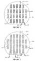
- FIG. 1Ais an enlarged schematic bottom view of a component constructed in accordance with the invention.
- FIG. 1Bis a enlarged schematic side elevation view of the component
- FIG. 1Cis an enlarged schematic cross sectional view of the component taken along section line 1 C— 1 C of FIG. 1A ;
- FIG. 1Dis an enlarged schematic cross sectional view of the component taken along section line 1 D— 1 D of FIG. 1C ;
- FIG. 1Eis an enlarged schematic cross sectional view of the component taken along section line 1 E— 1 E of FIG. 1C ;
- FIG. 1Fis an enlarged schematic cross sectional view of the component taken along section line 1 F— 1 F of FIG. 1C ;
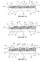
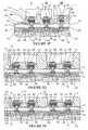
- FIG. 2is a plan view of a secondary wafer used in the fabrication of the component
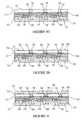
- FIGS. 2A-2Eare schematic cross sectional views taken along section line ( 2 A- 2 E)-( 2 A- 2 E) of FIG. 2 illustrating steps performed on dice on the secondary wafer during fabrication of the component;
- FIG. 3is a plan view of a base wafer used in the fabrication of the component
- FIGS. 3A-3Pare schematic cross sectional views taken along section line ( 3 A- 3 P)-( 3 A- 3 P) of FIG. 3 illustrating steps performed on a die on the base wafer during fabrication of the component with three different embodiments (I, II, III) illustrated in FIGS. 3M-3P ;
- FIGS. 3Q-3Vare schematic cross sectional views taken along section line ( 3 A- 3 P)-( 3 A- 3 P) of FIG. 3 illustrating steps performed on dice on the base wafer during fabrication of the component using embodiment II in FIGS. 3M-3P ;
- FIG. 4Ais a schematic cross sectional view equivalent to FIG. 1C of an alternate embodiment component having terminal contacts which comprise pins;
- FIG. 4Bis a schematic cross sectional view equivalent to FIG. 1C of an alternate embodiment component having two secondary dice stacked and bonded to one another and to a base die;
- FIG. 4Cis a schematic cross sectional view equivalent to FIG. 1C of an alternate embodiment component having direct connect base die with no redistribution layer;
- FIG. 4Dis a schematic cross sectional view equivalent to FIG. 1C of an alternate embodiment component having a center connect secondary die;
- FIG. 4Eis a schematic cross sectional view equivalent to FIG. 1C of an alternate embodiment component having an interconnect base die and stacked secondary dice;
- FIG. 4Fis a schematic cross sectional view equivalent to FIG. 1C of an alternate embodiment component having stacked base dice and a cap plate;
- FIG. 4Gis a schematic cross sectional view equivalent to FIG. 1C of an alternate embodiment component having an underfill layer configured as an encapsulant;
- FIG. 4His a schematic cross sectional view equivalent to FIG. 1C of an alternate embodiment component having stacked base dice and a cap plate with electronic components thereon;
- FIG. 5Ais a flow diagram illustrating broad steps in the fabrication method
- FIG. 5Bis a flow diagram illustrating steps performed on the secondary wafer in the fabrication method
- FIG. 5Cis a flow diagram illustrating steps performed on the base wafer in the fabrication method
- FIG. 5Dis a flow diagram illustrating steps for mounting the secondary dice to the base dice on the base wafer
- FIGS. 6A-6Gare flow diagrams illustrating steps of the fabrication method performed using different semiconductor fabrication equipment
- FIG. 7Ais a schematic plan view of a module system incorporating components constructed in accordance with the invention.
- FIG. 7Bis a schematic cross sectional view of the module system taken along section line 7 B— 7 B of FIG. 7A ;
- FIG. 8is a schematic cross sectional view of a system in a package incorporating components constructed in accordance with the invention.
- FIG. 9is a schematic cross sectional view of a computer system incorporating components constructed in accordance with the invention.
- FIG. 10is a schematic cross sectional view of a camcorder system incorporating components constructed in accordance with the invention.
- FIG. 11is a schematic cross sectional view of a camera system incorporating components constructed in accordance with the invention.
- FIG. 12is a schematic cross sectional view of a cellular phone system incorporating components constructed in accordance with the invention.
- FIG. 13is a schematic cross sectional view of a medical device system incorporating components constructed in accordance with the invention.
- semiconductor componentsrefers to an electronic element that includes a semiconductor die.
- Exemplary semiconductor componentsinclude semiconductor packages, semiconductor dice, BGA devices, and DDC devices.
- wafer level fabrication methodmeans a semiconductor fabrication method in which semiconductor wafers are used to make semiconductor components.
- the component 10includes a base die 12 (first die in the claims), and a secondary die 14 (second die in the claims). As will be further explained, the base die 12 and the secondary die 14 are stacked and bonded to one another.
- the base die 12 and the secondary die 14comprise active semiconductor dice having a desired electrical configuration.
- each die 12 , 14can comprise a high speed digital logic device, such as a dynamic random access memory (DRAM), a static random access memory (SRAM), a flash memory, a microprocessor, a digital signal processor (DSP), or an application specific integrated circuit (ASIC).
- each die 12 , 14can have a different configuration.
- the base die 12can comprise an application specific device
- the secondary die 14can comprise a memory device, such that the component 10 can be configured as a system in a package (SIP).
- SIPsystem in a package
- the base die 12can comprise an interconnect element with no integrated circuitry.
- component 10 E in FIG. 4Eincludes a base die 12 E with no integrated circuitry
- component 10 F in FIG. 4Fincludes a base die 12 F with no integrated circuitry.
- the component 10also includes an array of electrically conductive terminal contacts 18 configured for signal transmission to and from the component 10 .
- the terminal contacts 18are also sometimes referred to in the art as outer lead bonds (OLB).
- the terminal contacts 18comprise metal bumps or balls.
- the terminal contacts 18can also comprise pins, polymer bumps, spring contacts or any terminal contact or outer lead bond (OLB) known in the art.
- there are twelve terminal contacts 18arranged in a ball grid array (BGA) which includes two rows of six terminal contacts 18 each.
- BGAball grid array
- the terminal contacts 18can be arranged in any area array, such as a fine ball grid array (FBGA), an edge array or a peripheral array, containing any desired number of terminal contacts 18 .
- FBGAfine ball grid array
- FBGAfine ball grid array
- peripheral arraycontaining any desired number of terminal contacts 18 .
- the terminal contacts 18have outside diameters on the order of about 300 ⁇ m to 350 ⁇ m. This makes the terminal contacts 18 much larger in comparison to the other elements of the component 10 . However, for illustrative purposes the terminal contacts 18 are shown as being about the same size as other elements of the component 10 .
- the component 10also includes an encapsulant 16 formed on the base die 12 and on the edges of the secondary die 14 .
- the encapsulant 16can comprise a polymer material such as an epoxy, a silicone, a polyimide or a transfer molded underfill compound (MUF).
- these polymer materialscan include fillers such as silicates configured to reduce the coefficient of thermal expansion (CTE) and adjust the viscosity of the polymer material.
- the encapsulant 16can alternately comprise a laser imageable material, which can be patterned using a stereographic lithography process to be hereinafter described.
- the encapsulant 16can be eliminated.
- component 10 G in FIG. 4Gincludes an underfill layer 94 G which performs the function of the encapsulant 16 .
- the component 10also includes a polymer layer 20 formed on a circuit side 62 of the base die 12 proximate to the terminal contacts 18 .
- the polymer layer 20can comprise a polymer material such as an epoxy, a silicone, a polyimide, a photoimageable material such as a resist, or a laser imageable material.
- a polymer layer 20is sometimes referred to as a front side polymer (FSP).
- FSPfront side polymer
- the polymer layer 20performs a rigidifying function for the component 10 .
- the polymer layer 20can be configured as a polymer stencil for forming the terminal contacts 18 .
- the polymer layer 20can also be eliminated.
- a component 10 C in FIG. 4Chas no polymer layer 20 .
- the component 10also includes a plurality of interconnect contacts 22 , which function as internal signal transmission elements for transmitting signals between the base die 12 and the secondary die 14 .
- Each interconnect contact 22includes a bumped contact 24 on the secondary die 14 in electrical communication with a conductive via 26 on the base die 12 .
- Each interconnect contact 22also includes a bumped contact 86 on the base die 12 bonded to a conductive via 26 and to a bumped contact 24 on the secondary die 14 .
- the bumped contacts 24 and the bumped contacts 86are also referred to herein as inner lead bonds (ILB).
- the bumped contacts 24can have an outside diameter of only about 60 ⁇ m to 100 ⁇ m. This makes the bumped contacts 24 several times smaller than the terminal contacts 18 , which are about 300 ⁇ m to 350 ⁇ m in diameter. However, for illustrative purposes the bumped contacts 24 and the terminal contacts 18 are shown as being about the same size.
- the secondary die 14includes a plurality of die contacts 46 , such as interlevel bond pads, device bond pads, or redistribution pads, in electrical communication with the integrated circuits 32 ( FIG. 2A ) contained on the secondary die 14 .
- the bumped contacts 24are formed on the die contacts 46 , and the bumped contacts 24 are bonded to the conductive vias 26 .
- this arrangementis merely exemplary and the die contacts 46 can be formed in any desired pattern.
- a secondary die 14 Dincludes die contacts 46 formed along a center line of the die 14 D (center connect).
- the base die 12includes a plurality of die contacts 56 , such as interlevel bond pads, device bond pads, or redistribution pads, in electrical communication with the integrated circuits 60 ( FIG. 3A ) contained on the base die 12 .
- the pattern of the die contacts 56 on the base die 12matches the pattern of the die contacts 46 on the secondary die 14 .
- the component 10also includes a pattern of redistribution conductors 28 on the circuit side 62 of the base die 12 in electrical communication with the conductive vias 26 (FIG. 1 C), and with under bump metallization layers 58 for the terminal contacts 18 (FIG. 1 C).
- the redistribution conductors 28allow the pitch P1 of the terminal contacts 18 to be different than the pitch P2 of the die contacts 56 .
- the redistribution conductors 28can have a “fan out” configuration, such that the pitch P1 of the terminal contacts 18 can be greater than the pitch P2 of the die contacts 56 .
- the pitch P1 of the terminal contacts 18can be equal to, or less than, the pitch P2 of the die contacts 56 .
- the redistribution conductors 28change a standard pattern of the die contacts 56 to a customized pattern of the terminal contacts 18 .
- the redistribution conductors 28can be eliminated, and the terminal contacts 18 can be formed directly on the die contacts 56 .
- a component 10 C in FIG. 4Cdoes not have redistribution conductors 28 and the terminal contacts 18 are formed directly on the die contacts 56 on the base die 12 .
- the component 10also includes an underfill layer 94 which bonds the secondary die 14 to the base die 12 .
- the underfill layer 94can comprise a curable material or a tape material.
- the underfill layer 94can also perform the function of the encapsulant.
- a component 10 G in FIG. 4Gincludes an underfill layer 94 G which also functions as an encapsulant.
- FIGS. 2 and 3initial steps in a method for fabricating the component 10 are illustrated. Initially, as shown in FIG. 2 , a secondary wafer 30 containing a plurality of secondary dice 14 is provided. In addition, as shown in FIG. 3 , a base wafer 54 containing a plurality of base dice 12 is provided.
- each secondary die 14includes a plurality of integrated circuits 32 formed on a circuit side 34 thereof in a desired electrical configuration.
- the integrated circuits 32are formed in a silicon substrate 36 of the secondary wafer 30 using techniques that are well known in the art.
- the silicon substrate 36can comprise another semiconductor material such as gallium arsenide.
- the secondary wafer 30also includes an electrically insulating passivation layer 38 , such as a polymer, such as polyimide or BCB, an oxide such as silicon dioxide, or a glass, such as borophosphosilicate glass (BPSG).
- the passivation layer 38can be formed using techniques that are known in the art, such as by blanket deposition onto the secondary wafer 30 to a desired thickness.
- the passivation layer 38can include trenches 40 aligned with the streets between the secondary dice 14 .
- a mask layer 42is formed on the passivation layer 38 .
- the mask layer 42can comprise an electrically insulating polymer material, such as polyimide, photoimageable polyimide, BCB, epoxy or a resist formed with a pattern of openings 44 .
- the mask layer 42initially functions as a mask for etching the passivation layer 38 , and then as a permanent electrically insulating layer in the completed component 10 .
- the openings 44align with the die contacts 46 on the circuit side 34 of the secondary dice 14 . Following the etching step using the mask layer 42 , the openings 44 extend through the passivation layer 38 to the die contacts 46 .
- the secondary dice 14 on the secondary wafer 30can be probe tested using probes placed in the openings 44 in electrical communication with the die contacts 46 .
- the probe testingcan be performed using standard techniques and used to identify those secondary dice 14 on the secondary wafer 30 that are “good die”.
- each UBM layer 48includes an adhesion metal layer formed of a metal such as nickel, zinc, chromium, or palladium and a solder wettable metal layer formed of a metal such as palladium or gold.
- the UBM layers 48can be formed using a suitable deposition process such as electroless plating, electrolytic plating or chemical vapor deposition (CVD).
- the bumped contacts 24are formed on the UBM layers 48 .
- the bumped contacts 24can comprise a metal such as solder, deposited using a suitable process such as dipping, wave soldering, stenciling, or screen printing.
- a suitable processsuch as dipping, wave soldering, stenciling, or screen printing.
- One suitable process for forming the bumped contacts 24is described in U.S. Pat. No. 6,372,624 B1 to Farnworth et al., entitled “Method For Fabricating Solder Bumps By Wave Soldering”, which is incorporated herein by reference.
- the bumped contacts 24can also be formed using a bonding process such as ball bumping with a ball bumper apparatus or a wire bonder.
- the bumped contacts 24can comprise a conductive polymer formed using a suitable process such as stenciling or screen printing.
- the bumped contacts 24can comprise metal or metal plated pins formed on, or bonded to, the UBM layers 48 .
- the bumped contacts 24are referred to as inner lead bonds (ILB).
- the bumped contacts 24can be eliminated and the UBM layers 48 can be bonded directly to bumped contacts 86 ( FIG. 1C ) on the base die 12 .
- a singulating stepis performed to singulate or separate the secondary dice 14 from the secondary wafer 30 .
- One method for performing the singulating stepis to attach the secondary wafer 30 to a dicing tape 50 , and then cut kerfs 52 through the streets 31 ( FIG. 2 ) of the secondary wafer 30 using a dicing saw.
- the singulating stepalso controls the width of the secondary dice 14 .
- the singulating stepis illustrated as being performed to form the kerfs 52 ( FIG. 2D ) with a saw blade having a selected width SC1 (saw cut 1 ). As will be further explained, this width SC1 can be greater than the width of a saw blade SC2 ( FIG.
- the width of the secondary dice 14( FIG. 2 ) will thus be less than the width of the base dice 12 by an amount equal to the difference between the width SC1 ( FIG. 2 ) and the width SC2 (FIG. 3 ).
- the singulating stepcan be performed using another singulation method, such as cutting with a laser or a water jet, or be etching the secondary wafer 30 with a suitable wet or dry etchant.
- the secondary dice 14will be removed from the dicing tape 50 using a pick and place mechanism or other suitable apparatus and placed on the base wafer 54 (FIG. 3 ).
- the integrated circuits 32 on the secondary dice 14can be evaluated by wafer level testing of the secondary wafer 30 using equipment and techniques that are known in the art.
- the secondary wafer 30can be placed in a wafer prober having a probe card with probe contacts configured to electrically engage either the die contacts 46 or the bumped contacts 24 .
- the testingcan include functionality and parametric tests that are known in the art.
- the secondary dice 14can thus be evaluated and mapped prior to the singulating step.
- the singulated secondary dice 14can be further tested and burned-in, and certified as known good dice (KGD).
- each singulated secondary die 14includes the passivation layer 38 , the mask layer 42 and the bumped contacts 24 formed on the UBM layers 48 in electrical communication with the integrated circuits 32 .
- each base die 12includes a plurality of integrated circuits 60 formed on a circuit side 62 thereof in a desired electrical configuration.
- the integrated circuits 60are formed in a silicon substrate 64 of the base wafer 54 using techniques that are well known in the art.
- the silicon substrate 64can comprise another semiconductor material such as gallium arsenide.
- Each base die 12also includes the die contacts 56 in electrical communication with the integrated circuits 60 .
- the base wafer 54can be provided with no integrated circuits such that the base die 12 functions as an interconnect element but not as a active semiconductor device. For this reason the base wafer 54 is sometimes referred to in the description to follow as a through wafer interconnect (TWI).
- TWIthrough wafer interconnect
- the base wafer 54also includes an electrically insulating passivation layer 66 , such as a polymer, such as polyimide or BCB, an oxide such as silicon dioxide, or a glass, such as borophosphosilicate glass (BPSG).
- the passivation layer 66can be formed using techniques that are known in the art, such as by blanket deposition onto the base wafer 54 to a desired thickness.
- the redistribution conductors 28are formed in electrical communication with the die contacts 56 .
- the redistribution conductors 28can be formed using a subtractive process (e.g., etching) or an additive process (e.g., sputtering, or a combination of sputtering and plating) as is known in the art.
- Redistribution conductorsare widely used in semiconductor manufacture to customize the signal transmitting and terminal contact configuration of dice having standardized bond pad configurations.
- One suitable redistribution processis described in U.S. Pat. No. 5,851,911 to Farnworth, which is incorporated herein by reference.
- the redistribution conductors 28can be eliminated if the die contacts 56 have the required configuration.
- the die contacts 56can be made to accommodate the same pattern as the terminal contacts 18 (FIG. 1 C). In this case the redistribution conductors 28 can be eliminated.
- a first redistribution insulating layer 68is formed between the redistribution conductors 28 and the passivation layer 66
- a second redistribution insulating layer 70is formed on the redistribution conductors 28 .
- the first redistribution insulating layer 68 and the second redistribution insulating layer 70can comprise a polymer, such as polyimide or PBO (polybenzoxazole), deposited to a desired thickness using a suitable deposition process. If the redistribution conductors 28 are not formed, then the redistribution insulating layers 68 , 70 can be eliminated.
- the under bump metallization layers 58 for the terminal contacts 18are formed on the redistribution conductors 28 .
- the under bump metallization layers 58can comprise adhesion metal layers and solder wettable metal layers, formed substantially as previously described for under bump metallization layers 48 (FIG. 2 B).
- the under bump metallization layers 58have the pattern shown in FIG. 1 F.
- the polymer layer 20can be formed on the second redistribution insulating layer 70 .
- the polymer layer 20in addition to protecting the back side of the completed component 10 , also functions as a stiffener and rigidifying member as the base die 12 will subsequently be thinned.
- the polymer layer 20can be used as a stencil for forming the terminal contacts 18 .
- a representative thickness for the polymer layer 20can be from 25 ⁇ m to 150 ⁇ m. However, the polymer layer 20 is optional and can be omitted for some applications.
- the polymer layer 20can comprise a polymer patterned with openings 72 aligned with the under bump metallization layers 58 .
- One method for forming the polymer layer 20is with a stereo lithographic process.
- the polymer layer 20can comprise a laser imageable material, such as a “Cibatool SL 5530” resin manufactured by Ciba Specialty Chemicals Corporation, or an “SI40” laser imageable material manufactured by RPC Corporation.
- a layer of the laser imageable materialcan be blanket deposited on the base wafer 54 in viscous form using a suitable process such as spin on, and then exposed using a laser beam to define the openings 72 .
- the layercan then be developed to form the openings 72 in the exposed areas.
- the layercan then be rinsed, cleaned with a cleaning agent such as alcohol, and spun to remove excess material.
- the base water 54can then be placed in an oven, or alternately under a high intensity UV light, to cure the non-exposed material.
- a stereo lithography system for performing the imaging processis available from 3D Systems, Inc. of Valencia, Calif.
- stereographic lithographic processes(3-D) are described in U.S. application Ser. No. 09/259,142, to Farnworth et al. filed on Feb. 26, 1999, in U.S. application Ser. No. 09/652,340, to Farnworth et al. filed on Aug. 31, 2000, and in U.S. provisional application Ser. No. 60/425,567, to Farnworth et al. filed on Nov. 11, 2002, all of which are incorporated herein by reference.
- patterningcan be performed using a conventional photo tool configured to expose a photoimageable material using electromagnetic radiation in the G, H or I broadband.
- the polymer layer 20can be eliminated and the under fill layer 94 ( FIG. 3N ) can used to protect the base die 12 ( FIG. 1C ) and the edges of the secondary die 14 (FIG. 1 C).
- a protective tape 74is placed on the polymer layer 20 and covers the under bump metallization layers 58 .
- the protective tape 74protects the circuit side 62 of the base die 12 during the fabrication steps to be hereinafter described, and will be removed near the end of the fabrication process.
- the protective tape 74can comprise a high temperature chemical resistant tape, such as a polyimide or an epoxy tape, having an adhesive surface, such as an acrylic, and a desired thickness. Suitable tapes are manufactured by 3M Corporation and Dupont.
- vias 78are formed from a back side 76 of the base die 12 , and through the silicon substrate 64 to the die contacts 56 .
- the base die 12 in FIG. 3Ehas been flipped, such that the back side 76 faces up.
- One method for forming the vias 78uses laser machining to counter bore part way through the substrate 64 , followed by etching to complete the vias 78 .
- the vias 78align with the die contacts 56 , and with laser machining taper inward as the depth into the substrate 64 increases.
- the diameters of the vias 78can be from 10 ⁇ m to 2 mils or greater.
- the vias 78can also be laser machined or otherwise formed with a shape configured to facilitate deposition of a conductive material therein.
- the vias 78can include a large shallow portion, such as a trepan shaped counterbore, and a narrow portion which extends completely through the substrate 64 .
- the vias 78can then be filled with a metal such as nickel, and a solder alloy can be squeegeed, or otherwise deposited in the large shallow portion, to force the nickel through the narrow portion.
- a suitable laser system for performing the laser machining stepis manufactured by Electro Scientific, Inc., of Portland, Oreg and is designated a Model No. 2700.
- Another laser systemis manufactured by XSIL Corporation of Dublin, Ireland and is designated a Model No. “XCISE-200”.
- a representative laser fluence for forming the vias 78 through a silicon substrate having a thickness of about 28 mils (725 ⁇ m),is from 2 to 10 watts/per opening at a pulse duration of 20-25 ns, and at a repetition rate of up to several thousand per second.
- the wavelength of the laser beamcan be a standard UV wavelength (e.g., 355 nm).
- a thinning stepis performed in which the base wafer 54 is ground or polished from the back side 76 to thin the silicon substrate 64 .
- the thinning stepcan be performed using a mechanical planarization apparatus (e.g., a grinder).
- a mechanical planarization apparatuse.g., a grinder
- One suitable mechanical planarization apparatusis manufactured by Okamoto, and is designated a model no. VG502.
- the thinning stepcan also be performed using a chemical mechanical planarization (CMP) apparatus.
- CMPchemical mechanical planarization
- a suitable CMP apparatusis commercially available from a manufacturer such as Westech, SEZ, Plasma Polishing Systems, or TRUSI.
- the thinning stepcan also be performed using an etch back process, such as a wet etch process, a dry etch process or a plasma etching process either performed alone or in combination with mechanical planarization.
- the base wafer 54is thinned such that the silicon substrate 64 has a thickness Ts of about 280 ⁇ m.
- the thickness Tscan be as desired with from 100 ⁇ m to 600 ⁇ m being representative.
- an etching stepcan be performed, using a suitable wet or dry etchant, to extend the vias 78 completely through the silicon substrate 64 to the die contacts 56 .
- a suitable wet etchantis tetramethylammoniumhydroxide (TMAH).
- TMAHtetramethylammoniumhydroxide
- the wet etchantcan also further thin the silicon substrate 64 .
- the vias 78are laser machined to within about 10-50 ⁇ m of the die contacts 56 , and the etching step thins the base wafer 54 to a thickness Ts of about 250 ⁇ m.
- the etching stepalso cleans and enlarges the inside diameters of the vias 78 , and removes amorphous polysilicon and crystalline damaged silicon created in a heat affected zone (HAZ) due to heating by the laser beam.
- HAZheat affected zone
- insulating layers 80are formed on the inside diameters of the vies 78 , and on the back side 76 of the base wafer 54 .
- the insulating layers 80can be a grown or a deposited material.
- the insulating layers 80comprise a parylene polymer. Parylene polymers can be deposited from the vapor phase by a process similar to vacuum metallization at pressures of about 0.1 torr. Suitable polymers include parylene C, parylene N, and parylene D. Parylene is available from Advanced Coating of Tempe, Ariz.
- One suitable deposition apparatus for depositing parylene polymersis a portable parylene deposition system, designated a model PDS 2010 LABCOATER 2, manufactured by Specialty Coating Systems, of Indianapolis, Ind.
- the parylene polymeruniformly coat all exposed surfaces of the base wafer 54 to form the insulating layers 80 .
- a thickness range for the insulating layer 80can be from 0.10 to 76 ⁇ m or greater.
- the insulating layers 80can be an oxide, such as SiO 2 , formed by a growth process by exposure of the base wafer 54 to an O 2 atmosphere at an elevated temperature (e.g., 950° C.).
- the insulating layers 80can comprise an electrically insulating material, such as an oxide or a nitride, deposited using a deposition process such as CVD, or a polymer material deposited using a suitable deposition process such as screen printing.
- a subsequent laser drilling stepsubstantially as previously described, may be required to re-open the vias 78 .
- a resist layer 82is formed on the back side of the base wafer 54 , covering the insulating layers 80 and filling the vias 78 .
- the resist layer 82can comprise a suitable negative or positive tone polymer resist deposited to a desired thickness using a suitable deposition process, such as spin on.
- a suitable resist formulationis sold by, Shell Chemical under the trademark “EPON RESIN SU-8”.
- a laser machining processis performed to remove the resist layer 82 from the vias 78 , and to form indentations or openings in the die contacts 56 .
- the laser machining processcan be performed substantially as previously described and shown in FIG. 3E for initially forming the vias 78 .
- the vias 78are at least partially filled with a conductive material to form the conductive vias 26 .
- the conductive materialfills the indentations or openings formed in the contacts by the previous laser machining process.
- the conductive vias 78are thus in physical and electrical contact with the die contacts 56 .
- the conductive vias 26can be plugs that completely fill the vias 78 , or alternately, can be layers that cover just the inside surfaces or sidewalls of the vias 78 .
- the conductive materialcan comprise a highly conductive metal, such as aluminum, titanium, nickel, iridium, copper, gold, tungsten, silver, platinum, palladium, tantalum, molybdenum, tin, zinc and alloys of these metals including solder alloys.
- the above metalscan be deposited within the vias 78 using a deposition process, such as electroless deposition, CVD, or electrolytic deposition.
- the conductive vias 26can comprise a single metal or different layers of metal, such as a bonding layer and a non-oxidizing layer.
- the conductive materialcan comprise a conductive polymer, such as a metal filled silicone, or an isotropic epoxy.
- a conductive polymercan be deposited within the vias 78 , as a viscous material, and then cured as required.
- a suitable deposition processsuch as screen printing, or stenciling, can be used to deposit the conductive polymer into the vias 78 .
- Suitable conductive polymersare available from A.I. Technology, Trenton, N.J.; Sheldahl, Northfield, Minn.; and 3M, St. Paul, Minn.
- Another suitable conductive polymeris a nano-particle paste or ink, having metal nano-particles made of a highly conductive metal, such as aluminum. Nano-particle conductive polymers are commercially available from Superior Micropowders, of Albuquerque, N.Mex.
- the conductive vias 26can also be formed by depositing a metal such as nickel into the vias 78 , and then squeegeeing or otherwise forcing a solder allow into the vias 78 .
- the vias 78can include an enlarged portion, such as a trepan shaped counterbore, into which the solder can be squeegeed.
- the conductive vias 26can also be formed using the laser machining processes disclosed in U.S. Pat. No. 6,107,109 to Akram et al, U.S. Pat. No. 6,114,240 to Akram et al., and U.S. Pat. No. 6,294,837 B1 to Akram et al., all of which are incorporated herein by reference. Rather than a laser machining processes, the vias 78 can be formed using an etch mask and a suitable etchant. As another alternative, the conductive vias 26 can be formed as described in U.S. Pat. No. 6,313,531 B1 to Geusic et al., which is incorporated herein by reference.
- bumped contacts 86are formed on the conductive vias 26 .
- the bumped contacts 86can be formed using a deposition process or a bonding process, substantially as previously described for the terminal contacts 18 (FIG. 1 C).
- the bumped contacts 86comprise metal bumps or balls.
- the bumped contacts 86can also comprise metal pins, conductive polymer bumps, or other types of raised contacts that are known in the art.
- the bumped contacts 86can comprise one or more layers of material, such as under bump metal layers 87 and outer layers 98 made of a non-oxidizing metal such as gold.
- the bumped contacts 86are about the same size as the bumped contacts 24 ( FIG. 1C ) on the secondary dice 14 (60 ⁇ m to 100 ⁇ m in diameter).
- the bumped contacts 86 on the base dice 12can be omitted, and the bumped contacts 24 on the secondary dice 14 can be bonded directly to the under bump metal layers 87 using a bonding process to be hereinafter described.
- the base wafer 54can optionally be tested by placing probe contacts 84 in electrical communication with the bumped contacts 86 .
- Testing of the base wafer 54can be accomplished using wafer level testing techniques and equipment that are known in the art.
- the base wafer 54can be held in a wafer prober in electrical communication with a tester and having a probe card containing the probe contacts 84 .
- the testscan include functionality and parametric tests that are known in the art, and can identify and map defective base dice 12 contained on the base wafer 54 .
- U.S. Pat. No. 6,359,456 B1 to Husinee et al.describes exemplary wafer level testing equipment.
- the bumped contacts 86can be further processed to facilitate subsequent bonding to the mating bumped contacts 24 on the secondary dice 14 .
- Figure Millustrates three different embodiments designated I, II and III.
- the bumped contacts 86include solder tips 88 and the resist 82 remains on the base wafer 54 .
- the resist 82is stripped using a suitable stripper.
- solder bumps 90completely cover the bumped contacts 86 encircling and making physical contact with the conductive vias 26 .
- solder tips 88(embodiment I) or the solder bumps 90 (embodiment II) can be formed using a dipping, wave soldering, stenciling, or screen printing process substantially as previously described for bumped contacts 24 (FIG. 2 C).
- the resist 82is again stripped but the bumped contacts 86 are not covered with solder, such that outer layer 98 remains exposed.
- the underfill layer 94can be deposited on the base wafer 54 , and on the bumped contacts 86 with embodiments I or II, to facilitate subsequent bonding of the secondary dice 14 to the base wafer 54 .
- the underfill layer 94also functions to absorb thermal stresses generated between the secondary dice 14 and the base dice 12 in the completed component 10 .
- a conductive polymer adhesive 92can be used to bond the secondary dice 14 to the base wafer 54 .
- the underfill layer 94can comprise a conventional underfill polymer such as a curable silicone, epoxy or polyimide material.
- the underfill layer 94can also comprise a thermoset polymer underfill film, such as an underfill film manufactured by 3M Corporation of Minneapolis, Minn.
- the underfill layer 94can be deposited on the base wafer 54 in a viscous state using a conventional deposition apparatus, such as a material dispensing system having a computer controlled nozzle.
- a material dispensing systemhaving a computer controlled nozzle.
- One suitable systemis manufactured by Asymtek of Carlsbad, Calif.
- the conductive polymer adhesive 92can be deposited on the base wafer 54 to physically bond the secondary dice 14 to the base wafer 54 , and electrically connect the conductive vias 26 to the bumped contacts 24 on the secondary dice 14 .
- the conductive polymer adhesive 92can be deposited directly on embodiment III of the bumped contacts 86 .
- the conductive polymer adhesive 92includes electrically conductive particles 96 which make the electrical connections. Suitable conductive polymer adhesives are commercially available from A.I. Technology, Trenton, N.J.; and 3M, St. Paul, Minn.
- the good secondary dice 14are picked from the dicing tape 50 ( FIG. 2D ) and placed on the base wafer 54 .
- the bumped contacts 24 on the secondary dice 14are placed in proximity or physical contact with the solder tips 88 on the bumped contacts 86 on the base dice 12 .
- the bumped contacts 24 on the secondary dice 14are placed in proximity or physical contact with the solder bumps on the bumped contacts 86 on the base dice 12 .
- the bumped contacts 24 on the secondary dice 14are placed in proximity or physical contact with the bumped contacts 86 on the base dice 12 .
- a bonding stepis performed in which the base wafer 54 with the singulated secondary dice 14 thereon is heated in an oven to a selected temperature for a selected time period.
- the bonding stepis performed at a temperature sufficient to reflow the bumped contacts 24 on the secondary dice 14 and the bumped contacts 86 on the base dice 12 such that metallurgical bonds are formed there between.
- the bonding stepalso functions to cure the underfill layer 94 , and to adhesively bond the secondary dice 14 to the base dice 12 .
- the bonding stepis performed at a temperature sufficient to cure the conductive polymer adhesive 92 to adhesively bond the secondary dice 14 . If required curing can be performed by compressing the conductive polymer adhesive 92 to facilitate formation of separate electrical connections through the conductive particles 96 .
- FIG. 3Qis a cross section taken through a pair of secondary dice 14 , and a mating pair of base dice 12 on the base wafer 54 .
- the base dice 12have bumped contacts 86 configured as embodiment II, such that the resist layer 82 ( FIG. 3M ) has been stripped, and the solder bumps 90 ( FIG. 3M ) encircle the conductive vias 26 .
- the encapsulant 16can comprise a polymer material such as an epoxy, a silicone, a polyimide or a transfer molded underfill compound (MUF).
- these polymer materialscan include fillers such as silicates configured to reduce the coefficient of thermal expansion (CTE) and adjust the viscosity of the polymer material.
- the encapsulant 16can alternately comprise a laser imageable material, which can be patterned using a stereographic lithography substantially as previously described for polymer layer 20 . Alternately, the encapsulant 16 can comprise the underfill layer 94 .
- the thinning stepcan be performed by mechanically planarizing, and/or etching the adhesively bonded secondary dice 14 on the base wafer 54 .
- the secondary dice 14are ground, and/or etched, from the back side substantially as previously described and shown in the thinning step of FIG. 3F for the base dice 12 on the base wafer 54 .
- the resultant thickness Ts of the silicon substrate of the secondary dice 14can be as desired, with from 100 ⁇ m to 600 ⁇ m being representative.
- the protective tape 74( FIG. 3R ) is removed from the polymer layer 20 .
- the base wafer 54has been flipped such that the protective tape 74 faces up.
- the protective tape 74can be removed using a suitable stripper or by peeling it off of the base wafer 54 .
- a conductive material 100is deposited into the openings 72 in the polymer layer 20 and onto the die contacts 56 on the base dice 12 .
- the conductive material 100comprises solder or another metal deposited using a stenciling process.
- the conductive material 100is heated and reflows into balls or bumps which form the terminal contacts 18 .
- This reflow stepcan be performed by placing the base wafer 12 in an oven heated to a selected temperature for a selected time period.
- the polymer layer 20is optional, if it is not formed, another process such as screen printing, electroless deposition or electrolytic deposition can be employed to form the terminal contacts 18 .
- the polymer layer 20if used, also performs a protective and rigidifying function in the completed component 10 .
- a separate stencil(not shown) can be used in place of the polymer layer 20 .
- a singulating stepis performed to singulate the components 10 from the base wafer 54 .
- the singulating stepcan be performed such that the components 10 have symmetry in the X and Y directions.
- the encapsulant 16 for each component 10is symmetrical on either side of the secondary die 14 .
- the singulating stepcan be performed by placing the base wafer 54 on a dicing tape 104 , and singulating using a saw substantially as previously described for singulating the secondary wafer 30 (FIG. 2 D).
- the saw kerfs 102can be thinner than the saw kerfs 52 ( FIG. 2D ) to account for the size difference between the secondary dice 14 and the base dice 12 .
- Each secondary die 14has an outline (footprint) that is smaller than the outline (footprint) of its mating base die 12 .
- the component 10has an outline (footprint) that is substantially identical to that of the base die 12 contained therein.
- the component 10has a thickness T that is substantially equivalent to a conventional semiconductor die. In the illustrative embodiment the thickness T is from about 20 ⁇ m to 1500 ⁇ m.
- an alternate embodiment component 10 Pis illustrated.
- the component 10 Pis substantially similar to the component 10 (FIG. 1 C), and is constructed using substantially the same fabrication method to be hereinafter described.
- the component 10 Pincludes terminal contacts 18 P which comprise pins in an area array, such as a pin grid array, rather than bumps or balls as in component 10 (FIG. 1 C).
- the polymer layer 20FIG. 1C
- the terminal contacts 18 Pcan be welded, brazed, soldered, or otherwise bonded, to the under bump metallization layers 58 , using techniques and equipment that are known in the art.
- the component 10 Sis substantially similar to the component 10 (FIG. 1 C), and is constructed using substantially the same fabrication method illustrated in FIGS. 2A-2E and FIGS. 3A-3V .
- the component 10 Sincludes a first secondary die 14 S- 1 , and a second secondary die 14 S- 2 bonded to one another and to the base die 12 .
- the first secondary die 14 S- 1also includes conductive vias 26 S constructed substantially as previously described for the conductive vias 26 .
- bumped contacts 24 S on the second secondary die 14 S- 2are bonded to the conductive vias 26 S, substantially as previously described for bumped contacts 24 (FIG. 1 C).
- an encapsulant 16 Ssubstantially encapsulates the first secondary die 14 S- 1 and the second secondary die 14 S- 2 .
- the component 10 Scan include more than two stacked and bonded secondary dice 14 S- 1 , 14 S- 2 (e.g., 3 - 10 secondary dice).
- FIG. 4Can alternate embodiment component 10 C is illustrated.
- the component 10 Cis substantially similar to the component 10 (FIG. 1 C), and is constructed using substantially the same fabrication method illustrated in FIGS. 2A-2E and FIGS. 3A-3V .
- the component 10 Cdoes not include the redistribution conductors 56 (FIG. 1 C).
- the terminal contacts 18and the under bump metallization layers 58 for the terminal contacts 18 , are formed directly on the die contacts 56 for the base die 12 .
- the pattern of the terminal contacts 18matches the pattern of the die contacts 56 .
- the polymer layer 20FIG. 1C ) has been eliminated.
- FIG. 4Dan alternate embodiment component 10 D is illustrated.
- the component 10 Dis substantially similar to the component 10 (FIG. 1 C), and is constructed using substantially the same fabrication method illustrated in FIGS. 2A-2E and FIGS. 3A-3V .
- a secondary die 14 D of the component 10 Dincludes a single row of the die contacts 46 along a center line of the secondary die 14 D, rather than two rows of the die contacts 46 , as with the component 10 (FIG. 1 C).
- the terminal contacts 18fan out on either side of the die contacts 46 .
- FIG. 4Ean alternate embodiment component 10 E is illustrated.
- the component 10 Eis substantially similar to the component 10 S (FIG. 4 B), and is constructed using substantially the same fabrication method illustrated in FIGS. 2A-2E and FIGS. 3A-3V .
- a base interconnect 12 Eis not a semiconductor die and contains no integrated circuits, but merely performs a support and interconnect function.
- the base interconnect 12 Ecan comprise a semiconductor material, a ceramic material, or a plastic material.
- the base interconnect 12 Eincludes interconnect contacts 56 E, and conductive vias 26 E on which the under bump metallization layers 58 for the terminal contacts 18 are formed.
- the component 10 Fis substantially similar to the component 10 (FIG. 1 C), and is constructed using substantially the same fabrication method illustrated in FIGS. 2A-2E and FIGS. 3A-3V .
- the component 10 Fincludes two base dice 12 F 1 , 12 F 2 , which are stacked and bonded to one another.
- the base dice 12 F 1 , 12 F 2include conductive vias 26 F 1 , 26 F 2 , which function substantially as previously described for the conductive vias 26 ( FIG. 1C ) on the component 10 (FIG. 1 C).
- the component 10 Falso includes a cap plate 134 F bonded to the base die 12 F 2 using an underfill layer 94 F.
- the cap plate 134 Fcan comprise a material such as silicon, ceramic or plastic, on which patterns of conductors 136 F are formed.
- the cap plate 134 Fincludes bumped contacts 142 F in electrical communication with the conductors 136 F, and bonded to the conductive vias 26 F 2 on the base die 12 F 2 .
- the conductors 136 Felectrically connect (i.e., short) selected contacts 56 F (e.g., power and ground connections) on the base dice 12 F 1 , 12 F 2 to one another.
- the cap plate 134 Fcan comprise a semiconductor, a ceramic or a plastic material, on which the conductors 136 F and the bumped contacts 142 F can be formed using semiconductor fabrication techniques.
- the component 10 Gis substantially similar to the component 10 C (FIG. 4 C), and is constructed using substantially the same fabrication method illustrated in FIGS. 2A-2E and FIGS. 3A-3V .
- the component 10 Gincludes a base die 12 G and a secondary die 14 G.
- the component 10 Galso includes an underfill layer 84 G, which also functions as an encapsulant for the component 10 G.
- the underfill layer 84 Gcovers the back side of the base die 12 G and pots the secondary die 14 G to the base die 12 G.
- the component 10 His substantially similar to the component 10 F (FIG. 4 F), and is constructed using substantially the same fabrication method illustrated in FIGS. 2A-2E and FIGS. 3A-3V .
- the component 10 Hincludes two base dice 12 H 1 , 12 H 2 , which are stacked and bonded to one another.
- the base dice 12 H 1 , 12 H 2include conductive vias 26 H 1 , 26 H 2 , which function substantially as previously described for the conductive vias 26 ( FIG. 1C ) on the component 10 (FIG. 1 C).
- the component 10 Halso includes a cap plate 134 H bonded to the base die 12 H 2 using an underfill layer 94 H.
- the cap plate 134 Hcan comprise a material such as silicon, ceramic or plastic on which patterns of interlevel conductors 140 H are formed.
- the cap plate 134 Hincludes bumped contacts 142 H bonded to the conductive vias 26 H 2 on the base die 12 H 2 .
- the cap plate 134 Halso includes electronic components 138 H, such as capacitors, diodes or other electronic elements, in electrical communication with the interlevel conductors 140 H, and configured in a desired electronic circuit.
- the component 10 Halso includes an insulating layer 144 H, such as a deposited polymer, formed on the cap plate 134 H, and on the electronic components 138 H.
- FIGS. 5A-5Dflow charts of the fabrication method illustrated in FIGS. 2A-2E and 3 A- 3 V are shown.
- the fabrication methodis broken into three basic steps—Steps A, B and C.
- Step APrepare the secondary wafer 30 and singulate the secondary dice 14 from the secondary wafer 30 .
- Step BPrepare the base wafer 54 .
- Step CBond the secondary dice 14 to the base dice 12 on the base wafer 54 and singulate the components 10 from the base wafer 54 .
- the basic fabrication methodcan be modified by directly bonding the secondary wafer 30 to the base wafer 54 , and then singulating the components 10 from the bonded wafers.
- the base dice 12can be singulated, and the singulated secondary dice 14 can be bonded to the singulated base dice 12 .
- Step Ais broken into Steps A 1 -A 4 .
- Step A 1Form the mask layer 42 on the secondary wafer with the openings 44 therein aligned with the die contacts 46 (FIG. 2 A).
- Step A 2Provide test the secondary dice 14 on the secondary wafer 30 to identify “Good Dice” (FIG. 2 A).
- Step A 3 aForm the UBM layers 48 (FIG. 2 B).
- Step A 3 bForm the bumped contacts 24 on the UBM layers 48 (FIG. 2 C).
- Step A 4Singulate the secondary dice 14 from the secondary wafer 30 (FIG. 2 D).
- Step Bis broken into Steps B 1 -B 14 .
- Step B 1Form the RDL conductor 28 on the base wafer 54 (FIG. 3 A).
- Step B 2Form the UBM layers 58 on the RDL conductors 28 (FIG. 3 B).
- Step B 3Form the polymer layer 20 (optional) (FIG. 3 C).
- Step B 4Apply the protective tape 74 (FIG. 3 D).
- Step B 5Partially form the vias 78 (FIG. 3 E).
- Step 36Thin the base wafer 54 (FIG. 3 F).
- Step 37Etch to complete and clean the vias 78 (FIG. 3 G).
- Step B 8Form the insulating layers 80 (FIG. 3 H).
- Step B 9Form the resist layer 82 (FIG. 3 I).
- Step B 10Laser machine to open the insulated vias 78 (FIG. 3 J).
- Step B 11Form the conductive material in the vias 78 to form the conductive vias 26 (FIG. 3 K).
- Step B 12Form the bumped contacts 86 on the conductive vias 26 (FIG. 3 K).
- Step B 13Provide test the base dice 12 on the base wafer 54 (FIG. 3 K).
- Step 14Strip the resist 82 and form the solder tips 88 (FIG. 3 M).
- Step Cis broken into Steps C 1 a —C 8 .
- FIGS. 6A-6Gflow diagrams illustrating steps in the fabrication method performed using different semiconductor fabrication equipment are shown.
- the flow diagrams in FIGS. 6A-6Gdescribe exemplary equipment and processes used to align and bond the base dice 12 to the secondary dice 14 .
- the flow diagramsdescribe exemplary equipment and processes for forming the bumped contacts 24 (inner lead bonds—ILB) on the secondary dice 14 , the bumped contacts 86 (inner lead bonds—ILB) on the base dice 12 and the terminal contacts 18 (outer lead bonds—OLB) on the base dice 14 .
- the bumped contacts 24inner lead bonds—ILB
- the bumped contacts 86inner lead bonds—ILB
- OLBouter lead bonds
- FIG. 6Adescribes a die level bonding process using singulated base dice 12 and singulated secondary dice 14 .
- the processuses meniscus bumps for the bumped contacts 24 , 86 formed using a wave soldering process.
- the secondary wafer 30FIG. 2
- the UBM layers 48 ( FIG. 2B ) for the bumped contacts 24FIG. 2C
- the die contacts 46FIG. 2B
- a suitable processsuch as electroless deposition
- the bumped contacts 24FIG. 2C
- An exemplary wave soldering processis described in U.S.
- the secondary dice 14are singulated from the secondary wafer 30 using a suitable process such as sawing.
- the base wafer 54( FIG. 3 ) is provided.
- the base wafer 54can include the conductive vias 26 ( FIG. 3K ) and the insulating layers 80 ( FIG. 3H ) formed as previously described.
- the base wafer 54can include the redistribution conductors 28 . (FIG. 3 A), and the redistribution insulating layers 68 , 70 formed as previously described.
- the UBM layers 87 ( FIG. 3K ) for the bumped contacts 86 ( FIG. 3K )are formed on the conductive vias 26 .
- the base wafer 54is then singulated into the base dice 12 .
- the singulated dice 12 , 14are picked and placed into a tray, or onto a film frame tape, using a suitable manual or automated apparatus, such as a pick and place mechanism.
- a suitable manual or automated apparatussuch as a pick and place mechanism.
- the underfill layers 94are applied to the singulated base dice 12 using a suitable manual or automated apparatus.
- the singulated secondary dice 14 , and the singulated base dice 12are placed in a flip chip bonder.
- a flip chip bonderis described in U.S. Pat. No. 4,899,921 to Bendat et al., which is incorporated herein by reference.
- a suitable flip chip bonderis manufactured by Research Devices of Piscataway, N.J., and is designated an “M8 Visible Flip Chip Aligner Bonder”. As also shown in the middle portion of FIG. 6A , the flip chip bonder is used to bond the singulated base dice 12 to the singulated secondary dice 14 . Next, the terminal contacts 18 , are formed on the base dice 12 using a ball bumper and solder preforms.
- One suitable ball bumper, and the solder preforms as well,are manufactured by Pac Tech Packaging Technologies of Falkensee, Germany.
- FIG. 6Bdescribes a die level bonding process using singulated base dice 12 and singulated secondary dice 14 .
- the processuses a ball bumper to form the bumped contacts 24 , which are bonded directly to the UBM layers 87 on the base dice 12 .
- the secondary wafer 30FIG. 2
- the UBM layers 48 (FIG. 2 B) for the bumped contacts 24FIG. 2C
- the die contacts 46FIG. 2B
- a suitable processsuch as electroless deposition.
- the bumped contacts 24FIG. 2C
- One suitable ball bumpercapable of depositing solder bumps on the order of 80 ⁇ m or smaller, is manufactured by Pac Tech Packaging Technologies of Falkensee, Germany.
- the secondary dice 14are singulated from the secondary wafer 30 using a suitable process such as sawing.
- the singulated secondary dice 14are placed in a flip chip bonder such as the previously described “M8”, manufactured by Research Devices of Piscataway, N.J.
- the base wafer 54( FIG. 3 ) is provided.
- the base wafer 54can include the conductive vias 26 ( FIG. 3K ) and the insulating layers 80 ( FIG. 3H ) formed as previously described.
- the base wafer 54can include the redistribution conductors 28 (FIG. 3 A), and the redistribution insulating layers 68 , 70 formed as previously described.
- the UBM layers 87( FIG. 3K ) are formed on the conductive vias 26 .
- the base wafer 54is then singulated into the base dice 12 .
- the underfill layers 94are applied to the singulated base dice 12 using a suitable manual or automated apparatus.
- the singulated base dice 14are placed in the M8 flip chip bonder.
- the flip chip bonderis used to align and bond the bumped contacts 24 on the secondary dice 14 to the UBM layer 87 on the base dice 12 .
- the terminal contacts 18are formed on the base dice 12 using a ball bumper and solder preforms as previously described.
- FIG. 6Cdescribes a wafer level bonding process using singulated secondary dice 14 and the base wafer 54 .
- the processuses a first ball bumper to form the bumped contacts 24 on the secondary dice 14 , and a second ball bumper with a laser to bond the bumped contacts 24 to the UBM layers 87 on the base dice 12 .
- the secondary wafer 30FIG. 2
- the UBM layers 48FIG. 2B
- the bumped contacts 24FIG. 2C
- the bumped contacts 24FIG.
- the secondary dice 14are formed on the secondary dice 14 using a ball bumper.
- a ball bumperis the previously described 80 ⁇ m ball bumper manufactured by Pac Tech Packaging Technologies of Falkensee, Germany.
- the secondary dice 14are singulated from the secondary wafer 30 using a suitable process such as sawing.
- the base wafer 54( FIG. 3 ) is provided.
- the base wafer 54can include the conductive vias 26 (FIG. 3 K), and the insulating layers 80 ( FIG. 3H ) formed as previously described.
- the base wafer 54can include the redistribution conductors 28 (FIG. 3 A), and the redistribution insulating layers 68 , 70 formed as previously described.
- the UBM layers 87( FIG. 3K ) are formed on the conductive vias 26 .
- the base wafer 54is placed in a second ball bumper which includes a laser configured to heat through the base wafer 54 to heat and bond the bumped contacts 24 on the secondary dice 14 to the UBM layers 87 on the base dice 12 .
- a second ball bumperwhich includes a laser configured to heat through the base wafer 54 to heat and bond the bumped contacts 24 on the secondary dice 14 to the UBM layers 87 on the base dice 12 .
- One suitable ball bumperis manufacture by Pac Tech Packaging Technologies of Falkensee, Germany, and is designated the “LAPLACE”.
- the underfill layers 94are applied to the base wafer 54 mounted to the second ball bumper.
- the singulated secondary dice 14are aligned with and bonded to the base dice 12 on the base wafer 54 using the second ball bumper.
- the encapsulants 16are formed as previously described, and the terminal contacts 18 , are formed on the base dice 12 using a ball bumper and solder preforms as previously described.
- the components 10are singulated from the base wafer 54 , using a suitable process such as sawing.
- FIG. 6Ddescribes a wafer level bonding process using singulated secondary dice 14 which are bonded to the base wafer 54 .
- the process of FIG. 6Duses a ball bumper to form the bumped contacts 24 on the secondary dice 14 , and a flip chip bonder to bond the bumped contacts 24 on the secondary dice 14 to the UBM layers 87 on the base dice 12 on the base wafer 54 .
- the secondary wafer 30FIG. 2
- the UBM layers 48 ( FIG. 2B ) for the bumped contacts 24FIG. 2C
- the bumped contacts 24( FIG. 2C ) are formed on the secondary dice 14 using a ball bumper.
- a ball bumperis the previously described 80 ⁇ m ball bumper manufactured by Pac Tech Packaging Technologies of Falkensee, Germany.
- the secondary dice 14are singulated from the secondary wafer 30 using a suitable process such as sawing.
- the base wafer 54( FIG. 3 ) is provided.
- the base wafer 54can include the conductive vias 26 (FIG. 3 K), and the insulating layers 80 ( FIG. 3H ) formed as previously described.
- the base wafer 54can include the redistribution conductors 28 (FIG. 3 A), and the redistribution insulating layers 68 , 70 formed as previously described.
- the UBM layers 87( FIG. 3K ) are formed on the conductive vias 26 .
- the base wafer 54is placed in a flip chip bonder configured to bond the singulated secondary dice 14 to the base wafer 54 .
- One suitable wafer sized flip chip bonderis manufactured by Datacon Semiconductor Equipment GmbH, Radfeld, AT.
- the underfill layers 94are applied to the base wafer 54 mounted to the flip chip bonder.
- the singulated secondary dice 14are aligned with and bonded to the base dice 12 on the base wafer 54 using the flip chip bonder.
- the encapsulants 16are formed as previously described.
- the terminal contacts 18are formed on the base dice 12 using a ball bumper and solder preforms as previously described.
- the components 10are singulated from the base wafer 54 .
- FIG. 6Edescribes a wafer level bonding process in which the un-singulated secondary wafer 30 is bonded to the un-singulated base wafer 54 .
- the process described in FIG. 6Ealso uses a ball bumper to form the bumped contacts 24 on the secondary dice 14 on the secondary wafer 30 , and a wafer bonder to bond the bumped contacts 24 to the UBM layers 87 on the base dice 12 on the base wafer 54 .
- the secondary wafer 30FIG. 2
- the UBM layers 48 ( FIG. 2B ) for the bumped contacts 24FIG. 2C
- the bumped contacts 24are formed on the secondary dice 14 using a ball bumper.
- a ball bumperis the previously described 80 ⁇ m ball bumper manufactured by Pac Tech Packaging Technologies of Falkensee, Germany.
- the base wafer 54( FIG. 3 ) is provided.
- the base wafer 54can include the conductive vias 26 (FIG. 3 K), and the insulating layers 80 ( FIG. 3H ) formed as previously described.
- the base wafer 54can include the redistribution conductors 28 (FIG. 3 A), and the redistribution insulating layers 68 , 70 formed as previously described.
- the UBM layers 87( FIG. 3K ) are formed on the conductive vias 26 .
- the base wafer 54is placed in a wafer bonder configured to bond the secondary wafer 30 to the base wafer 54 .
- One suitable wafer bonderis a semiautomatic production bonder manufactured by EV Group Inc. of Phoenix, Ariz.
- the underfill layers 94are applied to the base wafer 54 mounted to the wafer bonder.
- the secondary wafer 30is aligned with and bonded to the base wafer using the wafer bonder.
- the terminal contacts 18are formed on the base dice 12 using a ball bumper and solder preforms as previously described.
- the components 10are singulated from the base wafer 54 using a suitable process such as sawing.
- FIG. 6Fdescribes a fabrication process for a three die component, such as component 10 E (FIG. 4 E), component 10 F ( FIG. 4F ) or component 10 H (FIG. 4 H).
- a die level bonding processis described using a pair of singulated base dice 12 and a singulated secondary dice 14 .
- the processcould be for a pair of secondary dice 14 and a single base die 12 .
- the processcould be for a single base die 12 , a single secondary die 14 and a cap plate 134 F ( FIG. 4F ) or 134 H (FIG. 4 H).
- the processuses meniscus bumps for the bumped contacts 24 on the secondary dice 14 and also for the bumped contacts 86 on one of the base dice 12 .
- the secondary wafer 30( FIG. 2 ) is provided.
- the UBM layers 48 ( FIG. 2B ) for the bumped contacts 24 ( FIG. 2C )are formed on the die contacts 46 ( FIG. 2B ) using a suitable process, such as electroless deposition.
- the bumped contacts 24 ( FIG. 2C )are formed on the secondary dice 14 using a wave soldering process, as previously described.
- the secondary dice 14are singulated from the secondary wafer 30 using a suitable process such as sawing.
- the base wafer 54 -# 1( FIG. 3 ) is provided.
- the base wafer 54 -# 1can include the conductive vias 26 ( FIG. 3K ) and the insulating layers 80 ( FIG. 3H ) formed as previously described.
- the base wafer 54 -# 1can include the redistribution conductors 28 (FIG. 3 A), and the redistribution insulating layers 68 , 70 formed as previously described.
- the UBM layers 87 ( FIG. 3K ) for the bumped contacts 86 ( FIG. 3K )are formed on the conductive vias 26 .
- the bumped contacts 86are formed as meniscus bumps using a wave soldering process as described above.
- Base wafer 54 -# 1is then singulated into the base dice 12 -# 1 , and the base dice 12 -# 1 are placed in the flip chip bonder, such as the previously described “M8” flip chip bonder manufactured by Research Devices of Piscataway, N.J.
- the base wafer 54 -# 2is provided, the UBM layers 87 are formed, and the base dice 12 -# 2 are singulated.
- the underfill layers 94are then formed on the base dice 12 -# 2 , and the base dice 12 -# 2 are placed in the flip chip bonder.
- the base dice 12 -# 1are then bonded to the base dice 12 -# 2 using the flip chip bonder to bond the bumped contacts 86 on the base dice 12 -# 1 to the UBM layers 87 on the base dice 12 -# 2 .
- the singulated secondary dice 14are placed in the flip chip bonder, and the secondary dice 14 are bonded to the bonded base dice 12 -# 1 and # 2 .
- the terminal contacts 18are formed on the base dice 12 -# 1 using a ball bumper and solder preforms as previously described.
- FIG. 6Gdescribes a fabrication process for a three die component, such as component 10 H ( FIG. 4H ) that also includes electronic components 138 H (FIG. 4 H), such as capacitors. Further, the process uses meniscus bumps for the bumped contacts 24 on the secondary dice 14 and also for the bumped contacts 86 on one of the base dice 12 .
- the secondary wafer 30( FIG. 2 ) is provided.
- the UBM layers 48 ( FIG. 2B ) for the bumped contacts 24 ( FIG. 2C )are formed on the die contacts 46 ( FIG. 2B ) using a suitable process, such as electroless deposition.
- the bumped contacts 24 ( FIG. 2C )are formed on the secondary dice 14 using a wave soldering process, as previously described.
- the secondary dice 14are singulated from the secondary wafer 30 using a suitable process such as sawing.
- the base wafer 54 -# 1( FIG. 3 ) is provided.
- the base wafer 54 -# 1can include the conductive vias 26 ( FIG. 3K ) and the insulating layers 80 ( FIG. 3H ) formed as previously described.
- the base wafer 54 -# 1can include the redistribution conductors 28 (FIG. 3 A), and the redistribution insulating layers 68 , 70 formed as previously described.
- the UBM layers 87 ( FIG. 3K ) for the bumped contacts 86 ( FIG. 3K )are formed on the conductive vias 26 .
- the bumped contacts 86are formed as meniscus bumps using a wave soldering process as described above.
- Base wafer 54 -# 1is then singulated into the base dice 12 -# 1 , and the base dice 12 -# 1 are placed in the flip chip bonder, such as the previously described “M8” flip chip bonder manufactured by Research Devices of Piscataway, N.J., or the flip chip bonder manufactured by Datacon Semiconductor Equipment GmbH, Radfeld, AT.
- the base wafer 54 -# 2is provided, the UBM layers 87 are formed, and the base dice 12 -# 2 are singulated.
- the underfill layer 94is then formed on the base dice 12 -# 2 , and the dice are placed in the flip chip bonder.
- the base dice 12 -# 1are then aligned and bonded to the base dice 12 -# 2 using the flip chip bonder to bond the bumped contacts 86 on the base dice 12 -# 1 to the UBM layers 87 on the base dice 12 -# 2 .
- pre-solder plated components 138 Hare bonded to the singulated secondary dice 14 .
- the singulated secondary dice 14are placed in the flip chip bonder, and the secondary dice 14 are bonded to the bonded base dice 12 -# 1 and # 2 .
- the terminal contacts 18are formed on the base dice 12 -# 1 using a ball bumper and solder preforms as previously described.
- the multi chip module system 106can be configured for performing a specific function such as memory storage.
- the multi chip module system 106includes a module substrate 108 having patterns of electrodes 114 ( FIG. 7B ) configured for flip chip mounting the components 10 to the module substrate 108 .
- the terminal contacts 18 on the components 10can be bonded to the electrodes 114 on the module substrate 108 using a suitable bonding process, such as solder reflow, thermode bonding or conductive polymer bonding.
- the electrodes 114are in electrical communication with conductors 110 formed on the module substrate 108 in a required circuit pattern.
- the conductors 110are in electrical communication with an edge connector 112 which provides connection points from the outside to the multi chip module system 106 .
- a system in a package 116that includes multiple components 10 is illustrated.
- the system in a package 116can be configured to perform a desired electrical function such as micro processing.
- each component 10can have a different electrical configuration, such as a micro controller, a microprocessor or a flash memory.
- the system in a package 116includes a package substrate 120 wherein the components 10 are flip chip mounted.
- the package substrate 120also includes electrodes and conductors (not shown) which electrically connect the components 10 in a required electrical configuration.
- the package substrate 120also includes package leads 118 in electrical communication with the components 10 .
- the system in a package 116also includes a package body 122 formed of a molded plastic, or other suitable material, which encapsulates the package substrate 120 and the components 10 .
- a computer system 124includes one or more components 10 , which can be mounted to the computer system 124 in a suitable manner.
- the components 10can be configured to perform a desired function in the computer system 124 such as memory, storage or micro processing.
- a digital camcorder system 126includes one or more components 10 , which can be mounted in a suitable manner, and configured to perform a desired circuit function in the camcorder system 126 .
- a camera system 128includes one or more components 10 , which can be mounted in a suitable manner, and configured to perform a desired circuit function in the camera system 128 .
- a cellular phone system 130includes one or more components 10 , which can be mounted to in a suitable manner, and configured to perform a desired circuit function in the cellular phone system 130 .
- a medical device system 132includes one or more components 10 , which can be mounted in a suitable manner, and configured to perform a desired circuit function in the medical device system 132 .
Landscapes
- Engineering & Computer Science (AREA)
- Microelectronics & Electronic Packaging (AREA)
- Power Engineering (AREA)
- Computer Hardware Design (AREA)
- General Physics & Mathematics (AREA)
- Physics & Mathematics (AREA)
- Condensed Matter Physics & Semiconductors (AREA)
- Manufacturing & Machinery (AREA)
- Chemical & Material Sciences (AREA)
- Materials Engineering (AREA)
- Internal Circuitry In Semiconductor Integrated Circuit Devices (AREA)
- Encapsulation Of And Coatings For Semiconductor Or Solid State Devices (AREA)
- Wire Bonding (AREA)
Abstract
Description
Claims (71)
Priority Applications (6)
| Application Number | Priority Date | Filing Date | Title |
|---|---|---|---|
| US10/403,937US6841883B1 (en) | 2003-03-31 | 2003-03-31 | Multi-dice chip scale semiconductor components and wafer level methods of fabrication |
| US10/730,333US7060526B2 (en) | 2003-03-31 | 2003-12-08 | Wafer level methods for fabricating multi-dice chip scale semiconductor components |
| US10/962,931US6998717B2 (en) | 2003-03-31 | 2004-10-11 | Multi-dice chip scale semiconductor components |
| US11/333,662US7224051B2 (en) | 2003-03-31 | 2006-01-17 | Semiconductor component having plate and stacked dice |
| US11/497,699US7459393B2 (en) | 2003-03-31 | 2006-08-02 | Method for fabricating semiconductor components with thinned substrate, circuit side contacts, conductive vias and backside contacts |
| US11/701,927US7498675B2 (en) | 2003-03-31 | 2007-02-02 | Semiconductor component having plate, stacked dice and conductive vias |
Applications Claiming Priority (1)
| Application Number | Priority Date | Filing Date | Title |
|---|---|---|---|
| US10/403,937US6841883B1 (en) | 2003-03-31 | 2003-03-31 | Multi-dice chip scale semiconductor components and wafer level methods of fabrication |
Related Child Applications (3)
| Application Number | Title | Priority Date | Filing Date |
|---|---|---|---|
| US10/730,333DivisionUS7060526B2 (en) | 2003-03-31 | 2003-12-08 | Wafer level methods for fabricating multi-dice chip scale semiconductor components |
| US10/962,931DivisionUS6998717B2 (en) | 2003-03-31 | 2004-10-11 | Multi-dice chip scale semiconductor components |
| US10/962,931ContinuationUS6998717B2 (en) | 2003-03-31 | 2004-10-11 | Multi-dice chip scale semiconductor components |
Publications (2)
| Publication Number | Publication Date |
|---|---|
| US20040256734A1 US20040256734A1 (en) | 2004-12-23 |
| US6841883B1true US6841883B1 (en) | 2005-01-11 |
Family
ID=32990079
Family Applications (6)
| Application Number | Title | Priority Date | Filing Date |
|---|---|---|---|
| US10/403,937Expired - Fee RelatedUS6841883B1 (en) | 2003-03-31 | 2003-03-31 | Multi-dice chip scale semiconductor components and wafer level methods of fabrication |
| US10/730,333Expired - Fee RelatedUS7060526B2 (en) | 2003-03-31 | 2003-12-08 | Wafer level methods for fabricating multi-dice chip scale semiconductor components |
| US10/962,931Expired - LifetimeUS6998717B2 (en) | 2003-03-31 | 2004-10-11 | Multi-dice chip scale semiconductor components |
| US11/333,662Expired - Fee RelatedUS7224051B2 (en) | 2003-03-31 | 2006-01-17 | Semiconductor component having plate and stacked dice |
| US11/497,699Expired - Fee RelatedUS7459393B2 (en) | 2003-03-31 | 2006-08-02 | Method for fabricating semiconductor components with thinned substrate, circuit side contacts, conductive vias and backside contacts |
| US11/701,927Expired - Fee RelatedUS7498675B2 (en) | 2003-03-31 | 2007-02-02 | Semiconductor component having plate, stacked dice and conductive vias |
Family Applications After (5)
| Application Number | Title | Priority Date | Filing Date |
|---|---|---|---|
| US10/730,333Expired - Fee RelatedUS7060526B2 (en) | 2003-03-31 | 2003-12-08 | Wafer level methods for fabricating multi-dice chip scale semiconductor components |
| US10/962,931Expired - LifetimeUS6998717B2 (en) | 2003-03-31 | 2004-10-11 | Multi-dice chip scale semiconductor components |
| US11/333,662Expired - Fee RelatedUS7224051B2 (en) | 2003-03-31 | 2006-01-17 | Semiconductor component having plate and stacked dice |
| US11/497,699Expired - Fee RelatedUS7459393B2 (en) | 2003-03-31 | 2006-08-02 | Method for fabricating semiconductor components with thinned substrate, circuit side contacts, conductive vias and backside contacts |
| US11/701,927Expired - Fee RelatedUS7498675B2 (en) | 2003-03-31 | 2007-02-02 | Semiconductor component having plate, stacked dice and conductive vias |
Country Status (1)
| Country | Link |
|---|---|
| US (6) | US6841883B1 (en) |
Cited By (248)
| Publication number | Priority date | Publication date | Assignee | Title |
|---|---|---|---|---|
| US20040080045A1 (en)* | 2002-10-28 | 2004-04-29 | Sharp Kabushiki Kaisha | Semiconductor device and chip-stack semiconductor device |
| US20040145051A1 (en)* | 2003-01-27 | 2004-07-29 | Klein Dean A. | Semiconductor components having stacked dice and methods of fabrication |
| US20040188819A1 (en)* | 2003-03-31 | 2004-09-30 | Farnworth Warren M. | Wafer level methods for fabricating multi-dice chip scale semiconductor components |
| US20050009329A1 (en)* | 2003-05-13 | 2005-01-13 | Kazumasa Tanida | Semiconductor chip production method, semiconductor device production method, semiconductor chip, and semiconductor device |
| US20050026335A1 (en)* | 2003-07-31 | 2005-02-03 | Fujitsu Limited | Method of fabricating semiconductor device and semiconductor device |
| US20050064624A1 (en)* | 2003-09-18 | 2005-03-24 | Minami Co., Ltd. | Method of manufacturing wafer level chip size package |
| US20050073035A1 (en)* | 2003-09-19 | 2005-04-07 | Moxham Stephen F. | Semiconductor component having stiffener and circuit decal and method of fabrication |
| US20050230804A1 (en)* | 2004-03-24 | 2005-10-20 | Kazumasa Tanida | Manufacturing method for semiconductor device, semiconductor device and semiconductor chip |
| US20060003547A1 (en)* | 2004-06-30 | 2006-01-05 | Kobrinsky Mauro J | Highly compliant plate for wafer bonding |
| US20060046468A1 (en)* | 2004-08-31 | 2006-03-02 | Salman Akram | Through-substrate interconnect fabrication methods and resulting structures and assemblies |
| US20060157853A1 (en)* | 2005-01-14 | 2006-07-20 | Ya-Ting Ho | Thermal bonding structure and manufacture process of flexible printed circuit board |
| US20060229097A1 (en)* | 2005-04-11 | 2006-10-12 | Microsoft Corporation | Computer-readable medium, method, and device for associating information with a contact |
| US20060228825A1 (en)* | 2005-04-08 | 2006-10-12 | Micron Technology, Inc. | Method and system for fabricating semiconductor components with through wire interconnects |
| US20060231927A1 (en)* | 2003-05-15 | 2006-10-19 | Kumamoto Technology & Industry Foundation | Semiconductor chip mounting body and manufacturing method thereof |
| US20060237843A1 (en)* | 2005-04-25 | 2006-10-26 | Masaaki Yanaka | BGA-type multilayer circuit wiring board |
| US20060261402A1 (en)* | 2005-05-20 | 2006-11-23 | Hang-Ting Lue | Air tunnel floating gate memory cell and method for making the same |
| US20060261446A1 (en)* | 2005-05-19 | 2006-11-23 | Micron Technology, Inc. | Backside method and system for fabricating semiconductor components with conductive interconnects |
| US20060267212A1 (en)* | 2005-05-09 | 2006-11-30 | Elpida Memory, Inc. | Semiconductor device |
| US20060281296A1 (en)* | 2005-06-14 | 2006-12-14 | Abhay Misra | Routingless chip architecture |
| US20060281219A1 (en)* | 2005-06-14 | 2006-12-14 | John Trezza | Chip-based thermo-stack |
| US20060278331A1 (en)* | 2005-06-14 | 2006-12-14 | Roger Dugas | Membrane-based chip tooling |
| US20060281363A1 (en)* | 2005-06-14 | 2006-12-14 | John Trezza | Remote chip attachment |
| US20060278996A1 (en)* | 2005-06-14 | 2006-12-14 | John Trezza | Active packaging |
| US20060278986A1 (en)* | 2005-06-14 | 2006-12-14 | John Trezza | Chip capacitive coupling |
| US20060278981A1 (en)* | 2005-06-14 | 2006-12-14 | John Trezza | Electronic chip contact structure |
| US20060281303A1 (en)* | 2005-06-14 | 2006-12-14 | John Trezza | Tack & fuse chip bonding |
| US20060278992A1 (en)* | 2005-06-14 | 2006-12-14 | John Trezza | Post & penetration interconnection |
| US20060289992A1 (en)* | 2005-06-27 | 2006-12-28 | Micron Technology, Inc. | Stacked semiconductor component, fabrication method and fabrication system |
| US20070001168A1 (en)* | 2004-08-27 | 2007-01-04 | Kirby Kyle K | Semiconductor components and assemblies including vias of varying lateral dimensions |
| US20070032061A1 (en)* | 2005-08-05 | 2007-02-08 | Farnworth Warren M | Methods of forming through-wafer interconnects and structures resulting therefrom |
| US20070048994A1 (en)* | 2005-09-01 | 2007-03-01 | Tuttle Mark E | Methods for forming through-wafer interconnects and structures resulting therefrom |
| US20070052094A1 (en)* | 2005-08-26 | 2007-03-08 | Samsung Electronics Co., Ltd. | Semiconductor wafer level chip package and method of manufacturing the same |
| US20070117264A1 (en)* | 2005-10-06 | 2007-05-24 | Texas Instruments Incorporated | Flip-Chip Semiconductor Device Manufacturing Method |
| US20070126091A1 (en)* | 2005-12-07 | 2007-06-07 | Wood Alan G | Semiconductor components having through wire interconnects (TWI) |
| US20070161235A1 (en)* | 2005-06-14 | 2007-07-12 | John Trezza | Back-to-front via process |
| WO2007092176A2 (en) | 2006-02-03 | 2007-08-16 | Micron Technology, Inc. | Methods for fabricating and filling conductive vias and conductive vias so formed |
| US20070235840A1 (en)* | 2006-03-30 | 2007-10-11 | Amram Eitan | Method, system, and apparatus for filling vias |
| US20070246819A1 (en)* | 2006-04-24 | 2007-10-25 | Micron Technology, Inc. | Semiconductor components and systems having encapsulated through wire interconnects (TWI) and wafer level methods of fabrication |
| US20070269994A1 (en)* | 2006-05-22 | 2007-11-22 | Micron Technology, Inc. | Methods of determining x-y spatial orientation of a semiconductor substrate comprising an integrated circuit, methods of positioning a semiconductor substrate comprising an integrated circuit, methods of processing a semiconductor substrate, and semiconductor devices |
| US20070271782A1 (en)* | 2004-07-01 | 2007-11-29 | Christian Block | Electrical Multilayer Component with Solder Contact |
| US20070281466A1 (en)* | 2006-06-06 | 2007-12-06 | John Trezza | Front-end processed wafer having through-chip connections |
| US20070281460A1 (en)* | 2006-06-06 | 2007-12-06 | Cubic Wafer, Inc. | Front-end processed wafer having through-chip connections |
| US20070278641A1 (en)* | 2005-06-14 | 2007-12-06 | John Trezza | Side Stacking Apparatus and Method |
| US20080006931A1 (en)* | 2006-07-06 | 2008-01-10 | Micron Technology, Inc. | Semiconductor constructions and assemblies, electronic systems, and methods of forming semiconductor constructions and assemblies |
| US20080030969A1 (en)* | 2006-07-19 | 2008-02-07 | Samsung Electro-Mechanics Co., Ltd. | Method for manufacturing a printed circuit board with a thin film capacitor embedded therein having a dielectric film by using laser lift-off, and printed circuit board with a thin film capacitor embedded therein manufactured thereby |
| US20080061441A1 (en)* | 2006-09-07 | 2008-03-13 | Chung-Shi Liu | Flexible via design to improve reliability |
| US20080138975A1 (en)* | 2006-12-08 | 2008-06-12 | Micron Technology, Inc. | Method and system for fabricating semiconductor components with through interconnects and back side redistribution conductors |
| US20080137439A1 (en)* | 2005-12-30 | 2008-06-12 | Micron Technology, Inc. | Configurable Inputs and Outputs for Memory Stacking System and Method |
| US20080157361A1 (en)* | 2006-12-28 | 2008-07-03 | Micron Technology, Inc. | Semiconductor components having through interconnects and methods of fabrication |
| US20080274589A1 (en)* | 2007-05-04 | 2008-11-06 | Chien-Hsiun Lee | Wafer-level flip-chip assembly methods |
| WO2008133943A1 (en)* | 2007-04-24 | 2008-11-06 | Flextronics Ap Llc | Small form factor modules using wafer level optics with bottom cavity and flip chip assembly |
| US20080272497A1 (en)* | 2007-05-04 | 2008-11-06 | Micron Technology, Inc. | Methods of forming conductive vias through substrates, and structures and assemblies resulting therefrom |
| US20080284970A1 (en)* | 2007-05-18 | 2008-11-20 | Semiconductor Energy Laboratory Co., Ltd. | Liquid crystal display device and manufacturing method thereof |
| US20080290435A1 (en)* | 2007-05-21 | 2008-11-27 | Micron Technology, Inc. | Wafer level lens arrays for image sensor packages and the like, image sensor packages, and related methods |
| US20090001600A1 (en)* | 2007-06-28 | 2009-01-01 | Freescale Semiconductor, Inc. | Electronic device including a plurality of singulated die and methods of forming the same |
| US20090002615A1 (en)* | 2007-06-15 | 2009-01-01 | Semiconductor Energy Laboratory Co., Ltd. | Display device |
| US20090015706A1 (en)* | 2007-04-24 | 2009-01-15 | Harpuneet Singh | Auto focus/zoom modules using wafer level optics |
| US20090014897A1 (en)* | 2003-05-15 | 2009-01-15 | Kumamoto Technology & Industry Foundation | Semiconductor chip package and method of manufacturing the same |
| US7521806B2 (en) | 2005-06-14 | 2009-04-21 | John Trezza | Chip spanning connection |
| US20090102021A1 (en)* | 2007-10-17 | 2009-04-23 | Chih-Hua Chen | Through-Silicon Vias and Methods for Forming the Same |
| US20090124072A1 (en)* | 2007-11-14 | 2009-05-14 | Samsung Electronics Co., Ltd. | Semiconductor device having through electrode and method of fabricating the same |
| US20090134500A1 (en)* | 2007-11-26 | 2009-05-28 | Chen-Cheng Kuo | Structures for Preventing Cross-talk Between Through-Silicon Vias and Integrated Circuits |
| US20090161402A1 (en)* | 2007-12-20 | 2009-06-25 | Hakjune Oh | Data storage and stackable configurations |
| US20090163790A1 (en)* | 2004-07-13 | 2009-06-25 | Dexcom, Inc. | Transcutaneous analyte sensor |
| US20090174079A1 (en)* | 2007-02-16 | 2009-07-09 | John Trezza | Plated pillar package formation |
| US20090186430A1 (en)* | 2007-05-24 | 2009-07-23 | Chih-Hua Chen | Test Patterns for Detecting Misalignment of Through-Wafer Vias |
| US20090193584A1 (en)* | 2008-02-05 | 2009-08-06 | Standard Textile Co., Inc. | Woven contoured bed sheet with elastomeric yarns |
| US20090213262A1 (en)* | 2008-02-22 | 2009-08-27 | Flextronics Ap, Llc | Attachment of wafer level optics |
| US20090236741A1 (en)* | 2008-03-19 | 2009-09-24 | Hsiang-Ming Huang | Conductive structure of a chip and method for manufacturing the same |
| US20090283871A1 (en)* | 2008-05-14 | 2009-11-19 | Hung-Pin Chang | System, Structure, and Method of Manufacturing a Semiconductor Substrate Stack |
| US20090283872A1 (en)* | 2008-05-13 | 2009-11-19 | Lin Chun-Te | Package structure of three-dimensional stacking dice and method for manufacturing the same |
| US20090321888A1 (en)* | 2007-12-06 | 2009-12-31 | Taiwan Semiconductor Manufacturing Company, Ltd. | Alignment for backside illumination sensor |
| US20100013077A1 (en)* | 2008-07-21 | 2010-01-21 | Samsaung Electronics Co., Ltd. | Semiconductor device |
| US20100038674A1 (en)* | 2008-08-18 | 2010-02-18 | Ding-Yuan Chen | Light-Emitting Diode With Current-Spreading Region |
| US20100044612A1 (en)* | 2008-08-20 | 2010-02-25 | Schuetz Udo | Tapping valve with a plastic valve housing for shipping and storage tanks for liquids |
| US20100062693A1 (en)* | 2008-09-05 | 2010-03-11 | Taiwan Semiconductor Manufacturing Co., Ltd. | Two step method and apparatus for polishing metal and other films in semiconductor manufacturing |
| US20100084747A1 (en)* | 2008-10-03 | 2010-04-08 | Chih-Hua Chen | Zigzag Pattern for TSV Copper Adhesion |
| US20100089578A1 (en)* | 2008-10-10 | 2010-04-15 | Nguyen Philip D | Prevention of Water Intrusion Into Particulates |
| US20100090304A1 (en)* | 2008-09-08 | 2010-04-15 | Taiwan Semiconductor Manufacturing Company, Ltd. | Bonding process for cmos image sensor |
| US20100096753A1 (en)* | 2008-10-21 | 2010-04-22 | Samsung Electronics Co., Ltd. | Through-silicon via structures providing reduced solder spreading and methods of fabricating the same |
| US20100117201A1 (en)* | 2008-11-13 | 2010-05-13 | Kai-Ming Ching | Cooling Channels in 3DIC Stacks |
| US20100144094A1 (en)* | 2008-12-05 | 2010-06-10 | Ming-Fa Chen | Method of Forming Stacked Dies |
| US20100140805A1 (en)* | 2008-12-10 | 2010-06-10 | Hung-Pin Chang | Bump Structure for Stacked Dies |
| US20100140776A1 (en)* | 2005-06-14 | 2010-06-10 | John Trezza | Triaxial through-chip connecton |
| US20100164109A1 (en)* | 2008-12-29 | 2010-07-01 | Wen-Chih Chiou | Backside Metal Treatment of Semiconductor Chips |
| US20100171203A1 (en)* | 2009-01-07 | 2010-07-08 | Taiwan Semiconductor Manufacturing Company | Robust TSV structure |
| US20100171197A1 (en)* | 2009-01-05 | 2010-07-08 | Hung-Pin Chang | Isolation Structure for Stacked Dies |
| US20100176494A1 (en)* | 2009-01-13 | 2010-07-15 | Ming-Fa Chen | Through-Silicon Via With Low-K Dielectric Liner |
| US20100187671A1 (en)* | 2009-01-26 | 2010-07-29 | Chuan-Yi Lin | Forming Seal Ring in an Integrated Circuit Die |
| US20100187670A1 (en)* | 2009-01-26 | 2010-07-29 | Chuan-Yi Lin | On-Chip Heat Spreader |
| US20100194014A1 (en)* | 2009-02-02 | 2010-08-05 | Jao Sheng Huang | Semiconductor Wafer Carrier |
| US20100193954A1 (en)* | 2009-02-04 | 2010-08-05 | Max Liu | Barrier Structures and Methods for Through Substrate Vias |
| US20100213560A1 (en)* | 2009-02-24 | 2010-08-26 | Taiwan Semiconductor Manufacturing Company, Ltd. | Pad design for backside illuminated image sensor |
| US20100214812A1 (en)* | 2009-02-24 | 2010-08-26 | Mosaid Technologies Incorporated | Stacked semiconductor devices including a master device |
| US20100220226A1 (en)* | 2009-02-24 | 2010-09-02 | Taiwan Semiconductor Manufacturing Company, Ltd. | Front side implanted guard ring structure for backside illuminated image sensor |
| US20100221873A1 (en)* | 2008-12-10 | 2010-09-02 | Stats Chippac, Ltd. | Semiconductor Device and Method of Forming an Interconnect Structure for 3-D Devices Using Encapsulant for Structural Support |
| US20100225002A1 (en)* | 2009-03-06 | 2010-09-09 | Taiwan Semiconductor Manufacturing Company, Ltd. | Three-Dimensional System-in-Package Architecture |
| US20100224966A1 (en)* | 2009-03-03 | 2010-09-09 | Taiwan Semiconductor Manufacturing Company, Ltd. | Stress Barrier Structures for Semiconductor Chips |
| US20100237502A1 (en)* | 2009-03-23 | 2010-09-23 | Taiwan Semiconductor Manufacturing Company, Ltd. | Barrier for Through-Silicon Via |
| US20100244284A1 (en)* | 2009-03-27 | 2010-09-30 | Taiwan Semiconductor Manufacturing Company, Ltd. | Method for ultra thin wafer handling and processing |
| US20100244247A1 (en)* | 2009-03-27 | 2010-09-30 | Taiwan Semiconductor Manufacturing Company, Ltd. | Via structure and via etching process of forming the same |
| US20100252934A1 (en)* | 2009-04-07 | 2010-10-07 | Taiwan Semiconductor Manufacturing Company, Ltd. | Three-Dimensional Semiconductor Architecture |
| US20100267217A1 (en)* | 2009-04-20 | 2010-10-21 | Taiwan Semiconductor Manufacturing Company, Ltd. | Backside Process for a Substrate |
| US20100276787A1 (en)* | 2009-04-30 | 2010-11-04 | Taiwan Semiconductor Manufacturing Company, Ltd. | Wafer Backside Structures Having Copper Pillars |
| US20100314758A1 (en)* | 2009-06-12 | 2010-12-16 | Taiwan Semiconductor Manufacturing Company, Ltd. | Through-silicon via structure and a process for forming the same |
| US20100330788A1 (en)* | 2009-06-30 | 2010-12-30 | Taiwan Semiconductor Manufacturing Company, Ltd. | Thin wafer handling structure and method |
| US20100330798A1 (en)* | 2009-06-26 | 2010-12-30 | Taiwan Semiconductor Manufacturing Company, Ltd. | Formation of TSV Backside Interconnects by Modifying Carrier Wafers |
| US20110006428A1 (en)* | 2009-07-08 | 2011-01-13 | Ching-Yu Lo | Liner Formation in 3DIC Structures |
| US20110027944A1 (en)* | 2009-07-30 | 2011-02-03 | Taiwan Semiconductor Maufacturing Company, Ltd. | Method of forming electrical connections |
| US20110035937A1 (en)* | 2009-08-14 | 2011-02-17 | Taiwan Semiconductor Manufacturing Company, Ltd. | Semiconductor Wafer Carrier and Method of Manufacturing |
| US20110037886A1 (en)* | 2009-08-14 | 2011-02-17 | Harpuneet Singh | Wafer level camera module with molded housing and method of manufacturing |
| US20110042825A1 (en)* | 2008-09-29 | 2011-02-24 | Hitachi, Ltd. | Semiconductor device |
| US20110049706A1 (en)* | 2009-09-03 | 2011-03-03 | Taiwan Semiconductor Manufacturing Company, Ltd. | Front Side Copper Post Joint Structure for Temporary Bond in TSV Application |
| US20110058340A1 (en)* | 2007-06-28 | 2011-03-10 | Yonggang Li | Method of forming a multilayer substrate core structure using sequential microvia laser drilling and substrate core structure formed according to the method |
| US20110065238A1 (en)* | 2009-09-14 | 2011-03-17 | Taiwan Semiconductor Manufacturing Company, Ltd. | Protection layer for adhesive material at wafer edge |
| US20110068466A1 (en)* | 2009-09-22 | 2011-03-24 | Taiwan Semiconductor Manufacturing Company, Ltd. | Wafer Backside Interconnect Structure Connected to TSVs |
| US20110078127A1 (en)* | 2009-09-27 | 2011-03-31 | Alibaba Group Holding Limited | Searching for information based on generic attributes of the query |
| US20110081749A1 (en)* | 2009-10-01 | 2011-04-07 | Taiwan Semiconductor Manufacturing Company, Ltd. | Surface modification for handling wafer thinning process |
| US20110084365A1 (en)* | 2009-10-09 | 2011-04-14 | Taiwan Semiconductor Manufacturing Company, Ltd. | Through Silicon Via (TSV) Wire Bond Architecture |
| US20110101527A1 (en)* | 2009-11-05 | 2011-05-05 | Taiwan Semiconductor Manufacturing Company, Ltd. | Mechanisms for forming copper pillar bumps |
| US20110108986A1 (en)* | 2009-11-09 | 2011-05-12 | Taiwan Semiconductor Manufacturing Company, Ltd. | Through-silicon via structure and a process for forming the same |
| US20110108940A1 (en)* | 2009-11-06 | 2011-05-12 | Taiwan Semiconductor Manufacturing Company, Ltd. | Method of fabricating backside-illuminated image sensor |
| US20110133335A1 (en)* | 2008-12-31 | 2011-06-09 | Taiwan Semiconductor Manufacturing Company, Ltd. | Through-Silicon Via With Air Gap |
| US20110133343A1 (en)* | 2008-08-06 | 2011-06-09 | Fujikura Ltd. | Semiconductor device |
| US20110168434A1 (en)* | 2010-01-12 | 2011-07-14 | International Business Machines Corporation | Bonded structure employing metal semiconductor alloy bonding |
| US20110169168A1 (en)* | 2009-02-24 | 2011-07-14 | Taiwan Semiconductor Manufacturing Company, Ltd. | Through-silicon via formed with a post passivation interconnect structure |
| US20110177655A1 (en)* | 2007-06-27 | 2011-07-21 | Taiwan Semiconductor Manufacturing Company, Ltd. | Formation of Through Via before Contact Processing |
| US20110193219A1 (en)* | 2010-02-09 | 2011-08-11 | Taiwan Seimconductor Manufacturing Company, Ltd. | Semiconductor device and semiconductor assembly with lead-free solder |
| US20110193221A1 (en)* | 2010-02-05 | 2011-08-11 | Taiwan Semiconductor Manufacturing Company, Ltd. | 3DIC Architecture with Interposer for Bonding Dies |
| US20110198721A1 (en)* | 2010-02-12 | 2011-08-18 | Taiwan Semiconductor Manufacturing Company, Ltd. | Method for thinning a wafer |
| US20110198747A1 (en)* | 2010-02-16 | 2011-08-18 | Taiwan Semicondcutor Manufactoring Company, Ltd. | Conductive pillar structure for semiconductor substrate and method of manufacture |
| US20110198638A1 (en)* | 2010-02-16 | 2011-08-18 | Taiwan Semiconductor Manufacturing Company, Ltd. | Light-emitting diode (led) package systems |
| US20110217841A1 (en)* | 2009-10-22 | 2011-09-08 | Taiwan Semiconductor Manufacturing Company, Ltd. | Method of forming through silicon via with dummy structure |
| US20110228154A1 (en)* | 2007-07-19 | 2011-09-22 | Flextronics Ap, Llc | Camera module back-focal length adjustment method and ultra compact components packaging |
| US20110233761A1 (en)* | 2009-07-30 | 2011-09-29 | Taiwan Semiconductor Manufacturing Company, Ltd. | Cu pillar bump with non-metal sidewall protection structure |
| US8174124B2 (en) | 2010-04-08 | 2012-05-08 | Taiwan Semiconductor Manufacturing Co., Ltd. | Dummy pattern in wafer backside routing |
| US8222139B2 (en) | 2010-03-30 | 2012-07-17 | Taiwan Semiconductor Manufacturing Company, Ltd. | Chemical mechanical polishing (CMP) processing of through-silicon via (TSV) and contact plug simultaneously |
| US8236584B1 (en) | 2011-02-11 | 2012-08-07 | Tsmc Solid State Lighting Ltd. | Method of forming a light emitting diode emitter substrate with highly reflective metal bonding |
| US8247906B2 (en) | 2009-07-06 | 2012-08-21 | Taiwan Semiconductor Manufacturing Company, Ltd. | Supplying power to integrated circuits using a grid matrix formed of through-silicon vias |
| US8319336B2 (en) | 2010-07-08 | 2012-11-27 | Taiwan Semiconductor Manufacturing Company, Ltd. | Reduction of etch microloading for through silicon vias |
| US8324738B2 (en) | 2009-09-01 | 2012-12-04 | Taiwan Semiconductor Manufacturing Company, Ltd. | Self-aligned protection layer for copper post structure |
| US8338939B2 (en) | 2010-07-12 | 2012-12-25 | Taiwan Semiconductor Manufacturing Company, Ltd. | TSV formation processes using TSV-last approach |
| US8362591B2 (en) | 2010-06-08 | 2013-01-29 | Taiwan Semiconductor Manufacturing Co., Ltd. | Integrated circuits and methods of forming the same |
| US8384215B2 (en) | 2010-12-30 | 2013-02-26 | Industrial Technology Research Institute | Wafer level molding structure |
| US8411459B2 (en) | 2010-06-10 | 2013-04-02 | Taiwan Semiconductor Manufacturing Company, Ltd | Interposer-on-glass package structures |
| US8441124B2 (en) | 2010-04-29 | 2013-05-14 | Taiwan Semiconductor Manufacturing Company, Ltd. | Cu pillar bump with non-metal sidewall protection structure |
| US8445296B2 (en) | 2011-07-22 | 2013-05-21 | Taiwan Semiconductor Manufacturing Company, Ltd. | Apparatus and methods for end point determination in reactive ion etching |
| US8456008B2 (en) | 2007-12-21 | 2013-06-04 | Taiwan Semiconductor Manufacturing Company, Ltd. | Structure and process for the formation of TSVs |
| US8455995B2 (en) | 2010-04-16 | 2013-06-04 | Taiwan Semiconductor Manufacturing Company, Ltd. | TSVs with different sizes in interposers for bonding dies |
| US8461045B2 (en) | 2008-10-09 | 2013-06-11 | Taiwan Semiconductor Manufacturing Company, Ltd. | Bond pad connection to redistribution lines having tapered profiles |
| US8466059B2 (en) | 2010-03-30 | 2013-06-18 | Taiwan Semiconductor Manufacturing Company, Ltd. | Multi-layer interconnect structure for stacked dies |
| US8471358B2 (en) | 2010-06-01 | 2013-06-25 | Taiwan Semiconductor Manufacturing Company, Ltd. | 3D inductor and transformer |
| US8476735B2 (en) | 2007-05-29 | 2013-07-02 | Taiwan Semiconductor Manufacturing Company, Ltd. | Programmable semiconductor interposer for electronic package and method of forming |
| WO2013103473A1 (en)* | 2012-01-06 | 2013-07-11 | Micron Technology, Inc. | Integrated circuit constructions having through substrate vias and methods of forming integrated circuit constructions having through substrate vias |
| US8487410B2 (en) | 2011-04-13 | 2013-07-16 | Taiwan Semiconductor Manufacturing Company, Ltd. | Through-silicon vias for semicondcutor substrate and method of manufacture |
| US8492260B2 (en) | 2010-08-30 | 2013-07-23 | Semionductor Components Industries, LLC | Processes of forming an electronic device including a feature in a trench |
| US8500182B2 (en) | 2010-06-17 | 2013-08-06 | Taiwan Semiconductor Manufacturing Company, Ltd. | Vacuum wafer carriers for strengthening thin wafers |
| US8502338B2 (en) | 2010-09-09 | 2013-08-06 | Taiwan Semiconductor Manufacturing Company, Ltd. | Through-substrate via waveguides |
| US8501587B2 (en) | 2009-01-13 | 2013-08-06 | Taiwan Semiconductor Manufacturing Company, Ltd. | Stacked integrated chips and methods of fabrication thereof |
| US8507940B2 (en) | 2010-04-05 | 2013-08-13 | Taiwan Semiconductor Manufacturing Company, Ltd. | Heat dissipation by through silicon plugs |
| US8507358B2 (en) | 2010-08-27 | 2013-08-13 | Taiwan Semiconductor Manufacturing Company, Ltd. | Composite wafer semiconductor |
| US8519538B2 (en) | 2010-04-28 | 2013-08-27 | Taiwan Semiconductor Manufacturing Company, Ltd. | Laser etch via formation |
| US8519409B2 (en) | 2010-11-15 | 2013-08-27 | Taiwan Semiconductor Manufacturing Company, Ltd. | Light emitting diode components integrated with thermoelectric devices |
| US20130223789A1 (en)* | 2012-02-23 | 2013-08-29 | Taiwan Semiconductor Manufacturing Company, Ltd. | Optical bench on substrate |
| US8525278B2 (en) | 2011-08-19 | 2013-09-03 | Taiwan Semiconductor Manufacturing Company, Ltd. | MEMS device having chip scale packaging |
| US8525343B2 (en) | 2010-09-28 | 2013-09-03 | Taiwan Semiconductor Manufacturing Company, Ltd. | Device with through-silicon via (TSV) and method of forming the same |
| US8531035B2 (en) | 2011-07-01 | 2013-09-10 | Taiwan Semiconductor Manufacturing Company, Ltd. | Interconnect barrier structure and method |
| US8546953B2 (en) | 2011-12-13 | 2013-10-01 | Taiwan Semiconductor Manufacturing Co., Ltd. | Through silicon via (TSV) isolation structures for noise reduction in 3D integrated circuit |
| US8545114B2 (en) | 2011-03-11 | 2013-10-01 | Digitaloptics Corporation | Auto focus-zoom actuator or camera module contamination reduction feature with integrated protective membrane |
| US8546235B2 (en) | 2011-05-05 | 2013-10-01 | Taiwan Semiconductor Manufacturing Company, Ltd. | Integrated circuits including metal-insulator-metal capacitors and methods of forming the same |
| US8546886B2 (en) | 2011-08-24 | 2013-10-01 | Taiwan Semiconductor Manufacturing Company, Ltd. | Controlling the device performance by forming a stressed backside dielectric layer |
| US8546254B2 (en) | 2010-08-19 | 2013-10-01 | Taiwan Semiconductor Manufacturing Company, Ltd. | Mechanisms for forming copper pillar bumps using patterned anodes |
| US8552485B2 (en) | 2011-06-15 | 2013-10-08 | Taiwan Semiconductor Manufacturing Company, Ltd. | Semiconductor structure having metal-insulator-metal capacitor structure |
| US8567837B2 (en) | 2010-11-24 | 2013-10-29 | Taiwan Semiconductor Manufacturing Company, Ltd. | Reconfigurable guide pin design for centering wafers having different sizes |
| US8580682B2 (en) | 2010-09-30 | 2013-11-12 | Taiwan Semiconductor Manufacturing Company, Ltd. | Cost-effective TSV formation |
| US8580647B2 (en) | 2011-12-19 | 2013-11-12 | Taiwan Semiconductor Manufacturing Company, Ltd. | Inductors with through VIAS |
| US8587127B2 (en) | 2011-06-15 | 2013-11-19 | Taiwan Semiconductor Manufacturing Company, Ltd. | Semiconductor structures and methods of forming the same |
| US20130313121A1 (en)* | 2012-05-25 | 2013-11-28 | Taiwan Semiconductor Manufacturing Company, Ltd. | Method of Forming Interconnects for Three Dimensional Integrated Circuit |
| US8604619B2 (en) | 2011-08-31 | 2013-12-10 | Taiwan Semiconductor Manufacturing Company, Ltd. | Through silicon via keep out zone formation along different crystal orientations |
| US8604491B2 (en) | 2011-07-21 | 2013-12-10 | Tsmc Solid State Lighting Ltd. | Wafer level photonic device die structure and method of making the same |
| US8610247B2 (en) | 2011-12-30 | 2013-12-17 | Taiwan Semiconductor Manufacturing Company, Ltd. | Structure and method for a transformer with magnetic features |
| US8618631B2 (en) | 2012-02-14 | 2013-12-31 | Taiwan Semiconductor Manufacturing Co., Ltd. | On-chip ferrite bead inductor |
| US8629563B2 (en) | 2007-07-16 | 2014-01-14 | Taiwan Semiconductor Manufacturing Company, Ltd. | Method for packaging semiconductor dies having through-silicon vias |
| US8629042B2 (en) | 2008-12-08 | 2014-01-14 | Taiwan Semiconductor Manufacturing Company, Ltd. | Method for stacking semiconductor dies |
| US20140021596A1 (en)* | 2012-07-18 | 2014-01-23 | Hong Kong Applied Science and Technology Research Institute Company Limited | Wafer-level device packaging |
| US8659126B2 (en) | 2011-12-07 | 2014-02-25 | Taiwan Semiconductor Manufacturing Company, Ltd. | Integrated circuit ground shielding structure |
| US8674883B2 (en) | 2011-05-24 | 2014-03-18 | Taiwan Semiconductor Manufacturing Company, Ltd. | Antenna using through-silicon via |
| US8674510B2 (en) | 2010-07-29 | 2014-03-18 | Taiwan Semiconductor Manufacturing Company, Ltd. | Three-dimensional integrated circuit structure having improved power and thermal management |
| US8693163B2 (en) | 2010-09-01 | 2014-04-08 | Taiwan Semiconductor Manufacturing Company, Ltd. | Cylindrical embedded capacitors |
| US8703609B2 (en) | 2007-08-24 | 2014-04-22 | Taiwan Semiconductor Manufacturing Company, Ltd. | Through-substrate via for semiconductor device |
| US8716128B2 (en) | 2011-04-14 | 2014-05-06 | Tsmc Solid State Lighting Ltd. | Methods of forming through silicon via openings |
| US8716131B2 (en) | 2008-08-05 | 2014-05-06 | Taiwan Semiconductor Manufacturing Company, Ltd. | Through silicon via layout |
| US8722540B2 (en) | 2010-07-22 | 2014-05-13 | Taiwan Semiconductor Manufacturing Company, Ltd. | Controlling defects in thin wafer handling |
| US20140145338A1 (en)* | 2011-05-24 | 2014-05-29 | Sony Corporation | Semiconductor device |
| US8748284B2 (en) | 2011-08-12 | 2014-06-10 | Taiwan Semiconductor Manufacturing Company, Ltd. | Method of manufacturing decoupling MIM capacitor designs for interposers |
| US8766409B2 (en) | 2011-06-24 | 2014-07-01 | Taiwan Semiconductor Manufacturing Co., Ltd. | Method and structure for through-silicon via (TSV) with diffused isolation well |
| US8773866B2 (en) | 2010-12-10 | 2014-07-08 | Taiwan Semiconductor Manufacturing Company, Ltd. | Radio-frequency packaging with reduced RF loss |
| US8803316B2 (en) | 2011-12-06 | 2014-08-12 | Taiwan Semiconductor Manufacturing Company, Ltd. | TSV structures and methods for forming the same |
| US8803322B2 (en) | 2011-10-13 | 2014-08-12 | Taiwan Semiconductor Manufacturing Company, Ltd. | Through substrate via structures and methods of forming the same |
| US8809073B2 (en) | 2011-08-03 | 2014-08-19 | Taiwan Semiconductor Manufacturing Company, Ltd. | Apparatus and methods for de-embedding through substrate vias |
| US8836116B2 (en) | 2010-10-21 | 2014-09-16 | Taiwan Semiconductor Manufacturing Company, Ltd. | Wafer level packaging of micro-electro-mechanical systems (MEMS) and complementary metal-oxide-semiconductor (CMOS) substrates |
| US8846499B2 (en) | 2010-08-17 | 2014-09-30 | Taiwan Semiconductor Manufacturing Company, Ltd. | Composite carrier structure |
| US8860114B2 (en) | 2012-03-02 | 2014-10-14 | Taiwan Semiconductor Manufacturing Company, Ltd. | Structure and method for a fishbone differential capacitor |
| US8866301B2 (en) | 2010-05-18 | 2014-10-21 | Taiwan Semiconductor Manufacturing Company, Ltd. | Package systems having interposers with interconnection structures |
| US8872345B2 (en) | 2011-07-07 | 2014-10-28 | Taiwan Semiconductor Manufacturing Company, Ltd. | Forming grounded through-silicon vias in a semiconductor substrate |
| US8890293B2 (en) | 2011-12-16 | 2014-11-18 | Taiwan Semiconductor Manufacturing Company, Ltd. | Guard ring for through vias |
| US8896136B2 (en) | 2010-06-30 | 2014-11-25 | Taiwan Semiconductor Manufacturing Company, Ltd. | Alignment mark and method of formation |
| US8896089B2 (en) | 2011-11-09 | 2014-11-25 | Taiwan Semiconductor Manufacturing Company, Ltd. | Interposers for semiconductor devices and methods of manufacture thereof |
| US8900994B2 (en) | 2011-06-09 | 2014-12-02 | Taiwan Semiconductor Manufacturing Company, Ltd. | Method for producing a protective structure |
| US8928159B2 (en) | 2010-09-02 | 2015-01-06 | Taiwan Semiconductor Manufacturing & Company, Ltd. | Alignment marks in substrate having through-substrate via (TSV) |
| US8928127B2 (en) | 2010-09-24 | 2015-01-06 | Taiwan Semiconductor Manufacturing Company, Ltd. | Noise decoupling structure with through-substrate vias |
| US8981533B2 (en) | 2012-09-13 | 2015-03-17 | Semiconductor Components Industries, Llc | Electronic device including a via and a conductive structure, a process of forming the same, and an interposer |
| US8994163B2 (en) | 2007-06-15 | 2015-03-31 | Micron Technology, Inc. | Semiconductor assemblies, stacked semiconductor devices, and methods of manufacturing semiconductor assemblies and stacked semiconductor devices |
| US8999179B2 (en) | 2010-07-13 | 2015-04-07 | Taiwan Semiconductor Manufacturing Company, Ltd. | Conductive vias in a substrate |
| US9018758B2 (en) | 2010-06-02 | 2015-04-28 | Taiwan Semiconductor Manufacturing Company, Ltd. | Cu pillar bump with non-metal sidewall spacer and metal top cap |
| US9041152B2 (en) | 2013-03-14 | 2015-05-26 | Taiwan Semiconductor Manufacturing Company, Ltd. | Inductor with magnetic material |
| US9048233B2 (en) | 2010-05-26 | 2015-06-02 | Taiwan Semiconductor Manufacturing Company, Ltd. | Package systems having interposers |
| US9059262B2 (en) | 2011-02-24 | 2015-06-16 | Taiwan Semiconductor Manufacturing Company, Ltd. | Integrated circuits including conductive structures through a substrate and methods of making the same |
| US9059026B2 (en) | 2010-06-01 | 2015-06-16 | Taiwan Semiconductor Manufacturing Company, Ltd. | 3-D inductor and transformer |
| KR101531181B1 (en)* | 2008-10-21 | 2015-06-25 | 삼성전자주식회사 | Stack package and method of manufacturing the same |
| US20150194400A1 (en)* | 2014-01-03 | 2015-07-09 | Taiwan Semiconductor Manufacturing Company, Ltd. | Barrier Structures Between External Electrical Connectors |
| US9087838B2 (en) | 2011-10-25 | 2015-07-21 | Taiwan Semiconductor Manufacturing Company, Ltd. | Structure and method for a high-K transformer with capacitive coupling |
| KR101553560B1 (en)* | 2008-11-26 | 2015-09-16 | 삼성전자주식회사 | Laminated package and method of manufacturing the same |
| US9139420B2 (en) | 2012-04-18 | 2015-09-22 | Taiwan Semiconductor Manufacturing Company, Ltd. | MEMS device structure and methods of forming same |
| US9153462B2 (en) | 2010-12-09 | 2015-10-06 | Taiwan Semiconductor Manufacturing Company, Ltd. | Spin chuck for thin wafer cleaning |
| US9159907B2 (en) | 2011-08-04 | 2015-10-13 | Taiwan Semiconductor Manufacturing Company, Ltd. | Hybrid film for protecting MTJ stacks of MRAM |
| US9184153B2 (en) | 2012-03-09 | 2015-11-10 | Industrial Technology Research Institute | Chip stack structure and method for fabricating the same |
| US9190325B2 (en) | 2010-09-30 | 2015-11-17 | Taiwan Semiconductor Manufacturing Company, Ltd. | TSV formation |
| US9293366B2 (en) | 2010-04-28 | 2016-03-22 | Taiwan Semiconductor Manufacturing Company, Ltd. | Through-substrate vias with improved connections |
| US9293521B2 (en) | 2012-03-02 | 2016-03-22 | Taiwan Semiconductor Manufacturing Co., Ltd. | Concentric capacitor structure |
| US9299594B2 (en) | 2010-07-27 | 2016-03-29 | Taiwan Semiconductor Manufacturing Company, Ltd. | Substrate bonding system and method of modifying the same |
| US9305769B2 (en) | 2009-06-30 | 2016-04-05 | Taiwan Semiconductor Manufacturing Company, Ltd. | Thin wafer handling method |
| US9312432B2 (en) | 2012-03-13 | 2016-04-12 | Tsmc Solid State Lighting Ltd. | Growing an improved P-GaN layer of an LED through pressure ramping |
| US9390949B2 (en) | 2011-11-29 | 2016-07-12 | Taiwan Semiconductor Manufacturing Company, Ltd. | Wafer debonding and cleaning apparatus and method of use |
| US9484211B2 (en) | 2013-01-24 | 2016-11-01 | Taiwan Semiconductor Manufacturing Company, Ltd. | Etchant and etching process |
| US9490133B2 (en) | 2013-01-24 | 2016-11-08 | Taiwan Semiconductor Manufacturing Company, Ltd. | Etching apparatus |
| US9524945B2 (en) | 2010-05-18 | 2016-12-20 | Taiwan Semiconductor Manufacturing Company, Ltd. | Cu pillar bump with L-shaped non-metal sidewall protection structure |
| US9618712B2 (en) | 2012-02-23 | 2017-04-11 | Taiwan Semiconductor Manufacturing Company, Ltd. | Optical bench on substrate and method of making the same |
| US9698105B2 (en) | 2014-10-11 | 2017-07-04 | Stmicroelectronics Pte Ltd | Electronic device with redistribution layer and stiffeners and related methods |
| US9812354B2 (en) | 2015-05-15 | 2017-11-07 | Semiconductor Components Industries, Llc | Process of forming an electronic device including a material defining a void |
| US10009528B2 (en) | 2011-02-24 | 2018-06-26 | Nan Chang O-Film Optoelectronics Technology Ltd | Autofocus camera module packaging with circuitry-integrated actuator system |
| US10381254B2 (en) | 2011-11-29 | 2019-08-13 | Taiwan Semiconductor Manufacturing Co., Ltd. | Wafer debonding and cleaning apparatus and method |
| US10879291B2 (en) | 2018-11-27 | 2020-12-29 | Raytheon Company | Stacked sensor with integrated capacitors |
| US11143961B1 (en)* | 2015-09-30 | 2021-10-12 | The University Of Manchester | Resist composition |
| US20220044998A1 (en)* | 2020-08-04 | 2022-02-10 | Micron Technology, Inc. | Low cost three-dimensional stacking semiconductor assemblies |
| US11264262B2 (en) | 2011-11-29 | 2022-03-01 | Taiwan Semiconductor Manufacturing Company, Ltd. | Wafer debonding and cleaning apparatus |
| US11521923B2 (en)* | 2018-05-24 | 2022-12-06 | Intel Corporation | Integrated circuit package supports |
| US12191221B2 (en) | 2021-07-05 | 2025-01-07 | Samsung Electronics Co., Ltd. | Semiconductor package |
Families Citing this family (446)
| Publication number | Priority date | Publication date | Assignee | Title |
|---|---|---|---|---|
| US7132741B1 (en)* | 2000-10-13 | 2006-11-07 | Bridge Semiconductor Corporation | Semiconductor chip assembly with carved bumped terminal |
| US7129575B1 (en)* | 2000-10-13 | 2006-10-31 | Bridge Semiconductor Corporation | Semiconductor chip assembly with bumped metal pillar |
| US6930256B1 (en) | 2002-05-01 | 2005-08-16 | Amkor Technology, Inc. | Integrated circuit substrate having laser-embedded conductive patterns and method therefor |
| US9691635B1 (en) | 2002-05-01 | 2017-06-27 | Amkor Technology, Inc. | Buildup dielectric layer having metallization pattern semiconductor package fabrication method |
| US7548430B1 (en) | 2002-05-01 | 2009-06-16 | Amkor Technology, Inc. | Buildup dielectric and metallization process and semiconductor package |
| US7633765B1 (en) | 2004-03-23 | 2009-12-15 | Amkor Technology, Inc. | Semiconductor package including a top-surface metal layer for implementing circuit features |
| US6791168B1 (en) | 2002-07-10 | 2004-09-14 | Micron Technology, Inc. | Semiconductor package with circuit side polymer layer and wafer level fabrication method |
| US6803303B1 (en) | 2002-07-11 | 2004-10-12 | Micron Technology, Inc. | Method of fabricating semiconductor component having encapsulated, bonded, interconnect contacts |
| JP4035034B2 (en)* | 2002-11-29 | 2008-01-16 | 株式会社ルネサステクノロジ | Semiconductor device and manufacturing method thereof |
| US8084866B2 (en) | 2003-12-10 | 2011-12-27 | Micron Technology, Inc. | Microelectronic devices and methods for filling vias in microelectronic devices |
| US7091124B2 (en) | 2003-11-13 | 2006-08-15 | Micron Technology, Inc. | Methods for forming vias in microelectronic devices, and methods for packaging microelectronic devices |
| KR100621992B1 (en)* | 2003-11-19 | 2006-09-13 | 삼성전자주식회사 | Wafer Level Stack Structure and Method of Heterogeneous Devices and System-in-Package Using the Same |
| US7425759B1 (en) | 2003-11-20 | 2008-09-16 | Bridge Semiconductor Corporation | Semiconductor chip assembly with bumped terminal and filler |
| US7538415B1 (en) | 2003-11-20 | 2009-05-26 | Bridge Semiconductor Corporation | Semiconductor chip assembly with bumped terminal, filler and insulative base |
| US7214886B2 (en)* | 2003-11-25 | 2007-05-08 | International Business Machines Corporation | High performance chip carrier substrate |
| US7098529B1 (en)* | 2004-01-07 | 2006-08-29 | Credence Systems Corporation | System and method for packaging a semiconductor device |
| DE102004008135A1 (en)* | 2004-02-18 | 2005-09-22 | Infineon Technologies Ag | Semiconductor device with a stack of semiconductor chips and method for producing the same |
| US7354863B2 (en)* | 2004-03-19 | 2008-04-08 | Micron Technology, Inc. | Methods of selectively removing silicon |
| US10811277B2 (en) | 2004-03-23 | 2020-10-20 | Amkor Technology, Inc. | Encapsulated semiconductor package |
| US11081370B2 (en) | 2004-03-23 | 2021-08-03 | Amkor Technology Singapore Holding Pte. Ltd. | Methods of manufacturing an encapsulated semiconductor device |
| US7229933B2 (en)* | 2004-03-31 | 2007-06-12 | Intel Corporation | Embossing processes for substrate imprinting, structures made thereby, and polymers used therefor |
| US20050247894A1 (en) | 2004-05-05 | 2005-11-10 | Watkins Charles M | Systems and methods for forming apertures in microfeature workpieces |
| US7232754B2 (en) | 2004-06-29 | 2007-06-19 | Micron Technology, Inc. | Microelectronic devices and methods for forming interconnects in microelectronic devices |
| TWI250596B (en)* | 2004-07-23 | 2006-03-01 | Ind Tech Res Inst | Wafer-level chip scale packaging method |
| US20070007637A1 (en)* | 2004-08-12 | 2007-01-11 | Marinov Valery R | Multi-layered substrate assembly with vialess electrical interconnect scheme |
| US7425499B2 (en) | 2004-08-24 | 2008-09-16 | Micron Technology, Inc. | Methods for forming interconnects in vias and microelectronic workpieces including such interconnects |
| SG120200A1 (en) | 2004-08-27 | 2006-03-28 | Micron Technology Inc | Slanted vias for electrical circuits on circuit boards and other substrates |
| US7300857B2 (en) | 2004-09-02 | 2007-11-27 | Micron Technology, Inc. | Through-wafer interconnects for photoimager and memory wafers |
| US7342312B2 (en) | 2004-09-29 | 2008-03-11 | Rohm Co., Ltd. | Semiconductor device |
| DE102004047730B4 (en)* | 2004-09-30 | 2017-06-22 | Advanced Micro Devices, Inc. | A method for thinning semiconductor substrates for the production of thin semiconductor wafers |
| KR100639702B1 (en)* | 2004-11-26 | 2006-10-30 | 삼성전자주식회사 | Packaged semiconductor die and manufacturing method thereof |
| JP4880218B2 (en)* | 2004-12-22 | 2012-02-22 | 三洋電機株式会社 | Circuit equipment |
| US7271482B2 (en) | 2004-12-30 | 2007-09-18 | Micron Technology, Inc. | Methods for forming interconnects in microelectronic workpieces and microelectronic workpieces formed using such methods |
| US7446422B1 (en)* | 2005-04-26 | 2008-11-04 | Amkor Technology, Inc. | Wafer level chip scale package and manufacturing method for the same |
| DE102005022017B3 (en)* | 2005-05-12 | 2006-10-26 | Infineon Technologies Ag | Semiconductor chip stack manufacturing method, involves holding stabilization layer at chemical mechanical polishing- or etched stop layer while thinning wafer of isolated semiconductor chips |
| US7351657B2 (en)* | 2005-06-10 | 2008-04-01 | Honeywell International Inc. | Method and apparatus for applying external coating to grid array packages for increased reliability and performance |
| US7795134B2 (en) | 2005-06-28 | 2010-09-14 | Micron Technology, Inc. | Conductive interconnect structures and formation methods using supercritical fluids |
| JP4659534B2 (en)* | 2005-07-04 | 2011-03-30 | 三菱電機株式会社 | Semiconductor device |
| US9601474B2 (en)* | 2005-07-22 | 2017-03-21 | Invensas Corporation | Electrically stackable semiconductor wafer and chip packages |
| DE102005042074A1 (en)* | 2005-08-31 | 2007-03-08 | Forschungsverbund Berlin E.V. | Method for producing plated-through holes in semiconductor wafers |
| US7622377B2 (en) | 2005-09-01 | 2009-11-24 | Micron Technology, Inc. | Microfeature workpiece substrates having through-substrate vias, and associated methods of formation |
| US7262134B2 (en) | 2005-09-01 | 2007-08-28 | Micron Technology, Inc. | Microfeature workpieces and methods for forming interconnects in microfeature workpieces |
| US7772115B2 (en)* | 2005-09-01 | 2010-08-10 | Micron Technology, Inc. | Methods for forming through-wafer interconnects, intermediate structures so formed, and devices and systems having at least one solder dam structure |
| US7863187B2 (en) | 2005-09-01 | 2011-01-04 | Micron Technology, Inc. | Microfeature workpieces and methods for forming interconnects in microfeature workpieces |
| US7348216B2 (en)* | 2005-10-04 | 2008-03-25 | International Business Machines Corporation | Rework process for removing residual UV adhesive from C4 wafer surfaces |
| US7637415B2 (en)* | 2005-10-31 | 2009-12-29 | General Electric Company | Methods and apparatus for assembling a printed circuit board |
| KR100753415B1 (en)* | 2006-03-17 | 2007-08-30 | 주식회사 하이닉스반도체 | Stack package |
| US7993972B2 (en) | 2008-03-04 | 2011-08-09 | Stats Chippac, Ltd. | Wafer level die integration and method therefor |
| JP3942190B1 (en)* | 2006-04-25 | 2007-07-11 | 国立大学法人九州工業大学 | Semiconductor device having double-sided electrode structure and manufacturing method thereof |
| US7670927B2 (en)* | 2006-05-16 | 2010-03-02 | International Business Machines Corporation | Double-sided integrated circuit chips |
| US8013342B2 (en)* | 2007-11-14 | 2011-09-06 | International Business Machines Corporation | Double-sided integrated circuit chips |
| US7557430B2 (en)* | 2006-05-25 | 2009-07-07 | Skyworks Solutions, Inc. | Semiconductor seal ring |
| KR100784498B1 (en)* | 2006-05-30 | 2007-12-11 | 삼성전자주식회사 | Laminated chip, manufacturing method thereof and semiconductor package having same |
| US7749899B2 (en) | 2006-06-01 | 2010-07-06 | Micron Technology, Inc. | Microelectronic workpieces and methods and systems for forming interconnects in microelectronic workpieces |
| JP4237207B2 (en)* | 2006-07-07 | 2009-03-11 | エルピーダメモリ株式会社 | Manufacturing method of semiconductor device |
| US7629249B2 (en) | 2006-08-28 | 2009-12-08 | Micron Technology, Inc. | Microfeature workpieces having conductive interconnect structures formed by chemically reactive processes, and associated systems and methods |
| US7902643B2 (en) | 2006-08-31 | 2011-03-08 | Micron Technology, Inc. | Microfeature workpieces having interconnects and conductive backplanes, and associated systems and methods |
| KR100750741B1 (en)* | 2006-09-15 | 2007-08-22 | 삼성전기주식회사 | Cap Wafer, Semiconductor Chip Having Same, and Manufacturing Method Thereof |
| KR100837554B1 (en)* | 2006-09-28 | 2008-06-12 | 동부일렉트로닉스 주식회사 | Semiconductor device and manufacturing method thereof |
| US7550857B1 (en) | 2006-11-16 | 2009-06-23 | Amkor Technology, Inc. | Stacked redistribution layer (RDL) die assembly package |
| US8569876B2 (en) | 2006-11-22 | 2013-10-29 | Tessera, Inc. | Packaged semiconductor chips with array |
| US7791199B2 (en)* | 2006-11-22 | 2010-09-07 | Tessera, Inc. | Packaged semiconductor chips |
| KR100817079B1 (en)* | 2006-12-05 | 2008-03-26 | 삼성전자주식회사 | Semiconductor chip module comprising a wafer level chip scale package, a method of manufacturing the same, and a wafer level chip scale package |
| US7727876B2 (en)* | 2006-12-21 | 2010-06-01 | Stats Chippac, Ltd. | Semiconductor device and method of protecting passivation layer in a solder bump process |
| JP2008160017A (en)* | 2006-12-26 | 2008-07-10 | Toshiba Corp | Semiconductor package and manufacturing method thereof |
| US7923823B2 (en)* | 2007-01-23 | 2011-04-12 | Infineon Technologies Ag | Semiconductor device with parylene coating |
| US8110906B2 (en)* | 2007-01-23 | 2012-02-07 | Infineon Technologies Ag | Semiconductor device including isolation layer |
| FR2911995B1 (en)* | 2007-01-30 | 2009-03-06 | 3D Plus Sa Sa | METHOD FOR INTERCONNECTING ELECTRONIC WAFERS |
| JP4269295B2 (en)* | 2007-02-20 | 2009-05-27 | セイコーエプソン株式会社 | Manufacturing method of fine structure |
| JP2008211125A (en) | 2007-02-28 | 2008-09-11 | Spansion Llc | Semiconductor device and its manufacturing method |
| US8405196B2 (en)* | 2007-03-05 | 2013-03-26 | DigitalOptics Corporation Europe Limited | Chips having rear contacts connected by through vias to front contacts |
| US7919410B2 (en)* | 2007-03-14 | 2011-04-05 | Aptina Imaging Corporation | Packaging methods for imager devices |
| US20090017576A1 (en)* | 2007-07-09 | 2009-01-15 | Swarnal Borthakur | Semiconductor Processing Methods |
| SG149710A1 (en) | 2007-07-12 | 2009-02-27 | Micron Technology Inc | Interconnects for packaged semiconductor devices and methods for manufacturing such devices |
| US20090026619A1 (en)* | 2007-07-24 | 2009-01-29 | Northrop Grumman Space & Mission Systems Corp. | Method for Backside Metallization for Semiconductor Substrate |
| KR100886712B1 (en)* | 2007-07-27 | 2009-03-04 | 주식회사 하이닉스반도체 | Semiconductor package and manufacturing method thereof |
| WO2009017835A2 (en)* | 2007-07-31 | 2009-02-05 | Tessera, Inc. | Semiconductor packaging process using through silicon vias |
| US8193092B2 (en) | 2007-07-31 | 2012-06-05 | Micron Technology, Inc. | Semiconductor devices including a through-substrate conductive member with an exposed end and methods of manufacturing such semiconductor devices |
| SG150410A1 (en) | 2007-08-31 | 2009-03-30 | Micron Technology Inc | Partitioned through-layer via and associated systems and methods |
| US8350382B2 (en)* | 2007-09-21 | 2013-01-08 | Infineon Technologies Ag | Semiconductor device including electronic component coupled to a backside of a chip |
| US7880310B2 (en)* | 2007-09-28 | 2011-02-01 | Intel Corporation | Direct device attachment on dual-mode wirebond die |
| US8815653B2 (en)* | 2007-12-03 | 2014-08-26 | Kolo Technologies, Inc. | Packaging and connecting electrostatic transducer arrays |
| US7884015B2 (en) | 2007-12-06 | 2011-02-08 | Micron Technology, Inc. | Methods for forming interconnects in microelectronic workpieces and microelectronic workpieces formed using such methods |
| US8084854B2 (en) | 2007-12-28 | 2011-12-27 | Micron Technology, Inc. | Pass-through 3D interconnect for microelectronic dies and associated systems and methods |
| US7948095B2 (en)* | 2008-02-12 | 2011-05-24 | United Test And Assembly Center Ltd. | Semiconductor package and method of making the same |
| US20090212420A1 (en)* | 2008-02-22 | 2009-08-27 | Harry Hedler | integrated circuit device and method for fabricating same |
| US20100053407A1 (en)* | 2008-02-26 | 2010-03-04 | Tessera, Inc. | Wafer level compliant packages for rear-face illuminated solid state image sensors |
| US20090212381A1 (en)* | 2008-02-26 | 2009-08-27 | Tessera, Inc. | Wafer level packages for rear-face illuminated solid state image sensors |
| EP2104138A1 (en)* | 2008-03-18 | 2009-09-23 | EV Group E. Thallner GmbH | Method for bonding chips onto a wafer |
| US8138577B2 (en)* | 2008-03-27 | 2012-03-20 | Hong Kong Applied Science And Technology Research Institute Co., Ltd. | Pulse-laser bonding method for through-silicon-via based stacking of electronic components |
| US8253230B2 (en) | 2008-05-15 | 2012-08-28 | Micron Technology, Inc. | Disabling electrical connections using pass-through 3D interconnects and associated systems and methods |
| US8829677B2 (en)* | 2010-10-14 | 2014-09-09 | Invensas Corporation | Semiconductor die having fine pitch electrical interconnects |
| US7678696B2 (en)* | 2008-08-08 | 2010-03-16 | International Business Machines Corporation | Method of making through wafer vias |
| US8138036B2 (en) | 2008-08-08 | 2012-03-20 | International Business Machines Corporation | Through silicon via and method of fabricating same |
| US8299566B2 (en) | 2008-08-08 | 2012-10-30 | International Business Machines Corporation | Through wafer vias and method of making same |
| US8035198B2 (en)* | 2008-08-08 | 2011-10-11 | International Business Machines Corporation | Through wafer via and method of making same |
| US8384224B2 (en) | 2008-08-08 | 2013-02-26 | International Business Machines Corporation | Through wafer vias and method of making same |
| JP5032456B2 (en)* | 2008-08-12 | 2012-09-26 | 新光電気工業株式会社 | Semiconductor device, interposer, and manufacturing method thereof |
| JP5350745B2 (en)* | 2008-10-21 | 2013-11-27 | 新光電気工業株式会社 | Wiring board |
| US8137995B2 (en)* | 2008-12-11 | 2012-03-20 | Stats Chippac, Ltd. | Double-sided semiconductor device and method of forming top-side and bottom-side interconnect structures |
| JP5420274B2 (en)* | 2009-03-02 | 2014-02-19 | パナソニック株式会社 | Semiconductor device and manufacturing method thereof |
| US7960827B1 (en) | 2009-04-09 | 2011-06-14 | Amkor Technology, Inc. | Thermal via heat spreader package and method |
| US8384426B2 (en) | 2009-04-14 | 2013-02-26 | Monolithic 3D Inc. | Semiconductor device and structure |
| US9577642B2 (en)* | 2009-04-14 | 2017-02-21 | Monolithic 3D Inc. | Method to form a 3D semiconductor device |
| US8058137B1 (en) | 2009-04-14 | 2011-11-15 | Monolithic 3D Inc. | Method for fabrication of a semiconductor device and structure |
| US9711407B2 (en) | 2009-04-14 | 2017-07-18 | Monolithic 3D Inc. | Method of manufacturing a three dimensional integrated circuit by transfer of a mono-crystalline layer |
| US8754533B2 (en) | 2009-04-14 | 2014-06-17 | Monolithic 3D Inc. | Monolithic three-dimensional semiconductor device and structure |
| US8362800B2 (en) | 2010-10-13 | 2013-01-29 | Monolithic 3D Inc. | 3D semiconductor device including field repairable logics |
| US8405420B2 (en) | 2009-04-14 | 2013-03-26 | Monolithic 3D Inc. | System comprising a semiconductor device and structure |
| US8378715B2 (en) | 2009-04-14 | 2013-02-19 | Monolithic 3D Inc. | Method to construct systems |
| US20110031997A1 (en)* | 2009-04-14 | 2011-02-10 | NuPGA Corporation | Method for fabrication of a semiconductor device and structure |
| US8362482B2 (en) | 2009-04-14 | 2013-01-29 | Monolithic 3D Inc. | Semiconductor device and structure |
| US8427200B2 (en)* | 2009-04-14 | 2013-04-23 | Monolithic 3D Inc. | 3D semiconductor device |
| US8395191B2 (en) | 2009-10-12 | 2013-03-12 | Monolithic 3D Inc. | Semiconductor device and structure |
| US8258810B2 (en) | 2010-09-30 | 2012-09-04 | Monolithic 3D Inc. | 3D semiconductor device |
| US9509313B2 (en)* | 2009-04-14 | 2016-11-29 | Monolithic 3D Inc. | 3D semiconductor device |
| US8669778B1 (en) | 2009-04-14 | 2014-03-11 | Monolithic 3D Inc. | Method for design and manufacturing of a 3D semiconductor device |
| US7986042B2 (en) | 2009-04-14 | 2011-07-26 | Monolithic 3D Inc. | Method for fabrication of a semiconductor device and structure |
| US8373439B2 (en)* | 2009-04-14 | 2013-02-12 | Monolithic 3D Inc. | 3D semiconductor device |
| US8187983B2 (en)* | 2009-04-16 | 2012-05-29 | Micron Technology, Inc. | Methods for fabricating semiconductor components using thinning and back side laser processing |
| WO2011153298A1 (en) | 2010-06-03 | 2011-12-08 | Hsio Technologies, Llc | Electrical connector insulator housing |
| US9276336B2 (en) | 2009-05-28 | 2016-03-01 | Hsio Technologies, Llc | Metalized pad to electrical contact interface |
| WO2010147939A1 (en) | 2009-06-17 | 2010-12-23 | Hsio Technologies, Llc | Semiconductor socket |
| US8955215B2 (en) | 2009-05-28 | 2015-02-17 | Hsio Technologies, Llc | High performance surface mount electrical interconnect |
| US9536815B2 (en) | 2009-05-28 | 2017-01-03 | Hsio Technologies, Llc | Semiconductor socket with direct selective metalization |
| US9414500B2 (en) | 2009-06-02 | 2016-08-09 | Hsio Technologies, Llc | Compliant printed flexible circuit |
| US9318862B2 (en) | 2009-06-02 | 2016-04-19 | Hsio Technologies, Llc | Method of making an electronic interconnect |
| US9276339B2 (en) | 2009-06-02 | 2016-03-01 | Hsio Technologies, Llc | Electrical interconnect IC device socket |
| WO2010147934A1 (en) | 2009-06-16 | 2010-12-23 | Hsio Technologies, Llc | Semiconductor die terminal |
| US8988093B2 (en) | 2009-06-02 | 2015-03-24 | Hsio Technologies, Llc | Bumped semiconductor wafer or die level electrical interconnect |
| US9613841B2 (en) | 2009-06-02 | 2017-04-04 | Hsio Technologies, Llc | Area array semiconductor device package interconnect structure with optional package-to-package or flexible circuit to package connection |
| US9603249B2 (en) | 2009-06-02 | 2017-03-21 | Hsio Technologies, Llc | Direct metalization of electrical circuit structures |
| WO2010141296A1 (en) | 2009-06-02 | 2010-12-09 | Hsio Technologies, Llc | Compliant printed circuit semiconductor package |
| WO2010141313A1 (en) | 2009-06-02 | 2010-12-09 | Hsio Technologies, Llc | Compliant printed circuit socket diagnostic tool |
| US9054097B2 (en) | 2009-06-02 | 2015-06-09 | Hsio Technologies, Llc | Compliant printed circuit area array semiconductor device package |
| WO2010141264A1 (en) | 2009-06-03 | 2010-12-09 | Hsio Technologies, Llc | Compliant wafer level probe assembly |
| US9232654B2 (en) | 2009-06-02 | 2016-01-05 | Hsio Technologies, Llc | High performance electrical circuit structure |
| WO2010141298A1 (en) | 2009-06-02 | 2010-12-09 | Hsio Technologies, Llc | Composite polymer-metal electrical contacts |
| WO2010141318A1 (en) | 2009-06-02 | 2010-12-09 | Hsio Technologies, Llc | Compliant printed circuit peripheral lead semiconductor test socket |
| US9320133B2 (en) | 2009-06-02 | 2016-04-19 | Hsio Technologies, Llc | Electrical interconnect IC device socket |
| US8987886B2 (en) | 2009-06-02 | 2015-03-24 | Hsio Technologies, Llc | Copper pillar full metal via electrical circuit structure |
| US9699906B2 (en) | 2009-06-02 | 2017-07-04 | Hsio Technologies, Llc | Hybrid printed circuit assembly with low density main core and embedded high density circuit regions |
| US8912812B2 (en) | 2009-06-02 | 2014-12-16 | Hsio Technologies, Llc | Compliant printed circuit wafer probe diagnostic tool |
| US8955216B2 (en) | 2009-06-02 | 2015-02-17 | Hsio Technologies, Llc | Method of making a compliant printed circuit peripheral lead semiconductor package |
| US9184145B2 (en) | 2009-06-02 | 2015-11-10 | Hsio Technologies, Llc | Semiconductor device package adapter |
| US9930775B2 (en) | 2009-06-02 | 2018-03-27 | Hsio Technologies, Llc | Copper pillar full metal via electrical circuit structure |
| US9136196B2 (en)* | 2009-06-02 | 2015-09-15 | Hsio Technologies, Llc | Compliant printed circuit wafer level semiconductor package |
| US8525346B2 (en) | 2009-06-02 | 2013-09-03 | Hsio Technologies, Llc | Compliant conductive nano-particle electrical interconnect |
| US9196980B2 (en) | 2009-06-02 | 2015-11-24 | Hsio Technologies, Llc | High performance surface mount electrical interconnect with external biased normal force loading |
| WO2012074963A1 (en) | 2010-12-01 | 2012-06-07 | Hsio Technologies, Llc | High performance surface mount electrical interconnect |
| US9231328B2 (en) | 2009-06-02 | 2016-01-05 | Hsio Technologies, Llc | Resilient conductive electrical interconnect |
| WO2011002709A1 (en) | 2009-06-29 | 2011-01-06 | Hsio Technologies, Llc | Compliant printed circuit semiconductor tester interface |
| WO2010147782A1 (en) | 2009-06-16 | 2010-12-23 | Hsio Technologies, Llc | Simulated wirebond semiconductor package |
| US8984748B2 (en) | 2009-06-29 | 2015-03-24 | Hsio Technologies, Llc | Singulated semiconductor device separable electrical interconnect |
| US8647963B2 (en)* | 2009-07-08 | 2014-02-11 | Taiwan Semiconductor Manufacturing Company, Ltd. | Structure and method of wafer level chip molded packaging |
| CN102034796B (en)* | 2009-10-01 | 2014-08-27 | 精材科技股份有限公司 | Chip package and manufacturing method thereof |
| US10366970B2 (en) | 2009-10-12 | 2019-07-30 | Monolithic 3D Inc. | 3D semiconductor device and structure |
| US10910364B2 (en) | 2009-10-12 | 2021-02-02 | Monolitaic 3D Inc. | 3D semiconductor device |
| US11018133B2 (en) | 2009-10-12 | 2021-05-25 | Monolithic 3D Inc. | 3D integrated circuit |
| US8581349B1 (en) | 2011-05-02 | 2013-11-12 | Monolithic 3D Inc. | 3D memory semiconductor device and structure |
| US12027518B1 (en) | 2009-10-12 | 2024-07-02 | Monolithic 3D Inc. | 3D semiconductor devices and structures with metal layers |
| US9099424B1 (en) | 2012-08-10 | 2015-08-04 | Monolithic 3D Inc. | Semiconductor system, device and structure with heat removal |
| US8148728B2 (en) | 2009-10-12 | 2012-04-03 | Monolithic 3D, Inc. | Method for fabrication of a semiconductor device and structure |
| US11374118B2 (en) | 2009-10-12 | 2022-06-28 | Monolithic 3D Inc. | Method to form a 3D integrated circuit |
| US10388863B2 (en) | 2009-10-12 | 2019-08-20 | Monolithic 3D Inc. | 3D memory device and structure |
| US10354995B2 (en) | 2009-10-12 | 2019-07-16 | Monolithic 3D Inc. | Semiconductor memory device and structure |
| US11984445B2 (en) | 2009-10-12 | 2024-05-14 | Monolithic 3D Inc. | 3D semiconductor devices and structures with metal layers |
| US8476145B2 (en) | 2010-10-13 | 2013-07-02 | Monolithic 3D Inc. | Method of fabricating a semiconductor device and structure |
| US10157909B2 (en) | 2009-10-12 | 2018-12-18 | Monolithic 3D Inc. | 3D semiconductor device and structure |
| US8536023B2 (en) | 2010-11-22 | 2013-09-17 | Monolithic 3D Inc. | Method of manufacturing a semiconductor device and structure |
| US10043781B2 (en) | 2009-10-12 | 2018-08-07 | Monolithic 3D Inc. | 3D semiconductor device and structure |
| US8742476B1 (en) | 2012-11-27 | 2014-06-03 | Monolithic 3D Inc. | Semiconductor device and structure |
| US8450804B2 (en) | 2011-03-06 | 2013-05-28 | Monolithic 3D Inc. | Semiconductor device and structure for heat removal |
| US7994062B2 (en)* | 2009-10-30 | 2011-08-09 | Sachem, Inc. | Selective silicon etch process |
| FR2953063B1 (en)* | 2009-11-20 | 2012-08-24 | St Microelectronics Tours Sas | METHOD FOR ENCAPSULATING ELECTRONIC COMPONENTS ON WAFER |
| TWI511253B (en)* | 2010-02-12 | 2015-12-01 | Xintec Inc | Chip package |
| US9099526B2 (en) | 2010-02-16 | 2015-08-04 | Monolithic 3D Inc. | Integrated circuit device and structure |
| US8026521B1 (en) | 2010-10-11 | 2011-09-27 | Monolithic 3D Inc. | Semiconductor device and structure |
| US8461035B1 (en) | 2010-09-30 | 2013-06-11 | Monolithic 3D Inc. | Method for fabrication of a semiconductor device and structure |
| US8298875B1 (en) | 2011-03-06 | 2012-10-30 | Monolithic 3D Inc. | Method for fabrication of a semiconductor device and structure |
| US8492886B2 (en) | 2010-02-16 | 2013-07-23 | Monolithic 3D Inc | 3D integrated circuit with logic |
| US8373230B1 (en) | 2010-10-13 | 2013-02-12 | Monolithic 3D Inc. | Method for fabrication of a semiconductor device and structure |
| US8541819B1 (en) | 2010-12-09 | 2013-09-24 | Monolithic 3D Inc. | Semiconductor device and structure |
| US8324511B1 (en)* | 2010-04-06 | 2012-12-04 | Amkor Technology, Inc. | Through via nub reveal method and structure |
| US20110248405A1 (en)* | 2010-04-09 | 2011-10-13 | Qualcomm Incorporated | Selective Patterning for Low Cost through Vias |
| TWI427753B (en)* | 2010-05-20 | 2014-02-21 | Advanced Semiconductor Eng | Package structure and package process |
| US8758067B2 (en) | 2010-06-03 | 2014-06-24 | Hsio Technologies, Llc | Selective metalization of electrical connector or socket housing |
| US9350093B2 (en) | 2010-06-03 | 2016-05-24 | Hsio Technologies, Llc | Selective metalization of electrical connector or socket housing |
| US9689897B2 (en) | 2010-06-03 | 2017-06-27 | Hsio Technologies, Llc | Performance enhanced semiconductor socket |
| US10159154B2 (en) | 2010-06-03 | 2018-12-18 | Hsio Technologies, Llc | Fusion bonded liquid crystal polymer circuit structure |
| KR101088824B1 (en)* | 2010-06-16 | 2011-12-06 | 주식회사 하이닉스반도체 | Module substrate, memory module having same and method for forming memory module |
| US20110309481A1 (en)* | 2010-06-18 | 2011-12-22 | Rui Huang | Integrated circuit packaging system with flip chip mounting and method of manufacture thereof |
| US8791575B2 (en) | 2010-07-23 | 2014-07-29 | Tessera, Inc. | Microelectronic elements having metallic pads overlying vias |
| US9640437B2 (en) | 2010-07-23 | 2017-05-02 | Tessera, Inc. | Methods of forming semiconductor elements using micro-abrasive particle stream |
| US8796135B2 (en) | 2010-07-23 | 2014-08-05 | Tessera, Inc. | Microelectronic elements with rear contacts connected with via first or via middle structures |
| US9219005B2 (en) | 2011-06-28 | 2015-12-22 | Monolithic 3D Inc. | Semiconductor system and device |
| US10217667B2 (en) | 2011-06-28 | 2019-02-26 | Monolithic 3D Inc. | 3D semiconductor device, fabrication method and system |
| US8901613B2 (en) | 2011-03-06 | 2014-12-02 | Monolithic 3D Inc. | Semiconductor device and structure for heat removal |
| US8642416B2 (en) | 2010-07-30 | 2014-02-04 | Monolithic 3D Inc. | Method of forming three dimensional integrated circuit devices using layer transfer technique |
| US9953925B2 (en) | 2011-06-28 | 2018-04-24 | Monolithic 3D Inc. | Semiconductor system and device |
| US8847380B2 (en) | 2010-09-17 | 2014-09-30 | Tessera, Inc. | Staged via formation from both sides of chip |
| US8610259B2 (en) | 2010-09-17 | 2013-12-17 | Tessera, Inc. | Multi-function and shielded 3D interconnects |
| US8884434B2 (en)* | 2010-09-27 | 2014-11-11 | Infineon Technologies Ag | Method and system for improving reliability of a semiconductor device |
| US8163581B1 (en) | 2010-10-13 | 2012-04-24 | Monolith IC 3D | Semiconductor and optoelectronic devices |
| US11482440B2 (en) | 2010-12-16 | 2022-10-25 | Monolithic 3D Inc. | 3D semiconductor device and structure with a built-in test circuit for repairing faulty circuits |
| US12362219B2 (en) | 2010-11-18 | 2025-07-15 | Monolithic 3D Inc. | 3D semiconductor memory device and structure |
| US10497713B2 (en) | 2010-11-18 | 2019-12-03 | Monolithic 3D Inc. | 3D semiconductor memory device and structure |
| US8273610B2 (en) | 2010-11-18 | 2012-09-25 | Monolithic 3D Inc. | Method of constructing a semiconductor device and structure |
| TW201216439A (en)* | 2010-10-08 | 2012-04-16 | Universal Scient Ind Co Ltd | Chip stacked structure |
| US11257867B1 (en) | 2010-10-11 | 2022-02-22 | Monolithic 3D Inc. | 3D semiconductor device and structure with oxide bonds |
| US10290682B2 (en) | 2010-10-11 | 2019-05-14 | Monolithic 3D Inc. | 3D IC semiconductor device and structure with stacked memory |
| US11227897B2 (en) | 2010-10-11 | 2022-01-18 | Monolithic 3D Inc. | Method for producing a 3D semiconductor memory device and structure |
| US11024673B1 (en) | 2010-10-11 | 2021-06-01 | Monolithic 3D Inc. | 3D semiconductor device and structure |
| US10896931B1 (en) | 2010-10-11 | 2021-01-19 | Monolithic 3D Inc. | 3D semiconductor device and structure |
| US8114757B1 (en) | 2010-10-11 | 2012-02-14 | Monolithic 3D Inc. | Semiconductor device and structure |
| US11469271B2 (en) | 2010-10-11 | 2022-10-11 | Monolithic 3D Inc. | Method to produce 3D semiconductor devices and structures with memory |
| US11600667B1 (en) | 2010-10-11 | 2023-03-07 | Monolithic 3D Inc. | Method to produce 3D semiconductor devices and structures with memory |
| US11158674B2 (en) | 2010-10-11 | 2021-10-26 | Monolithic 3D Inc. | Method to produce a 3D semiconductor device and structure |
| US11018191B1 (en) | 2010-10-11 | 2021-05-25 | Monolithic 3D Inc. | 3D semiconductor device and structure |
| US11315980B1 (en) | 2010-10-11 | 2022-04-26 | Monolithic 3D Inc. | 3D semiconductor device and structure with transistors |
| US8283215B2 (en) | 2010-10-13 | 2012-10-09 | Monolithic 3D Inc. | Semiconductor and optoelectronic devices |
| US11855114B2 (en) | 2010-10-13 | 2023-12-26 | Monolithic 3D Inc. | Multilevel semiconductor device and structure with image sensors and wafer bonding |
| US10978501B1 (en) | 2010-10-13 | 2021-04-13 | Monolithic 3D Inc. | Multilevel semiconductor device and structure with waveguides |
| US11043523B1 (en) | 2010-10-13 | 2021-06-22 | Monolithic 3D Inc. | Multilevel semiconductor device and structure with image sensors |
| US11984438B2 (en) | 2010-10-13 | 2024-05-14 | Monolithic 3D Inc. | Multilevel semiconductor device and structure with oxide bonding |
| US11694922B2 (en) | 2010-10-13 | 2023-07-04 | Monolithic 3D Inc. | Multilevel semiconductor device and structure with oxide bonding |
| US11437368B2 (en) | 2010-10-13 | 2022-09-06 | Monolithic 3D Inc. | Multilevel semiconductor device and structure with oxide bonding |
| US10833108B2 (en) | 2010-10-13 | 2020-11-10 | Monolithic 3D Inc. | 3D microdisplay device and structure |
| US12094892B2 (en) | 2010-10-13 | 2024-09-17 | Monolithic 3D Inc. | 3D micro display device and structure |
| US11163112B2 (en) | 2010-10-13 | 2021-11-02 | Monolithic 3D Inc. | Multilevel semiconductor device and structure with electromagnetic modulators |
| US11869915B2 (en) | 2010-10-13 | 2024-01-09 | Monolithic 3D Inc. | Multilevel semiconductor device and structure with image sensors and wafer bonding |
| US10998374B1 (en) | 2010-10-13 | 2021-05-04 | Monolithic 3D Inc. | Multilevel semiconductor device and structure |
| US11164898B2 (en) | 2010-10-13 | 2021-11-02 | Monolithic 3D Inc. | Multilevel semiconductor device and structure |
| US11855100B2 (en) | 2010-10-13 | 2023-12-26 | Monolithic 3D Inc. | Multilevel semiconductor device and structure with oxide bonding |
| US11327227B2 (en) | 2010-10-13 | 2022-05-10 | Monolithic 3D Inc. | Multilevel semiconductor device and structure with electromagnetic modulators |
| US10679977B2 (en) | 2010-10-13 | 2020-06-09 | Monolithic 3D Inc. | 3D microdisplay device and structure |
| US11063071B1 (en) | 2010-10-13 | 2021-07-13 | Monolithic 3D Inc. | Multilevel semiconductor device and structure with waveguides |
| US11929372B2 (en) | 2010-10-13 | 2024-03-12 | Monolithic 3D Inc. | Multilevel semiconductor device and structure with image sensors and wafer bonding |
| US12360310B2 (en) | 2010-10-13 | 2025-07-15 | Monolithic 3D Inc. | Multilevel semiconductor device and structure with oxide bonding |
| US11605663B2 (en) | 2010-10-13 | 2023-03-14 | Monolithic 3D Inc. | Multilevel semiconductor device and structure with image sensors and wafer bonding |
| US10943934B2 (en) | 2010-10-13 | 2021-03-09 | Monolithic 3D Inc. | Multilevel semiconductor device and structure |
| US8379458B1 (en) | 2010-10-13 | 2013-02-19 | Monolithic 3D Inc. | Semiconductor device and structure |
| US12080743B2 (en) | 2010-10-13 | 2024-09-03 | Monolithic 3D Inc. | Multilevel semiconductor device and structure with image sensors and wafer bonding |
| US11404466B2 (en) | 2010-10-13 | 2022-08-02 | Monolithic 3D Inc. | Multilevel semiconductor device and structure with image sensors |
| US9197804B1 (en) | 2011-10-14 | 2015-11-24 | Monolithic 3D Inc. | Semiconductor and optoelectronic devices |
| US11133344B2 (en) | 2010-10-13 | 2021-09-28 | Monolithic 3D Inc. | Multilevel semiconductor device and structure with image sensors |
| TWI501365B (en)* | 2010-10-13 | 2015-09-21 | Ind Tech Res Inst | Package unit, stacking structure thereof and manufacturing method thereof |
| CN102456673A (en)* | 2010-10-25 | 2012-05-16 | 环旭电子股份有限公司 | Stacked structure of chip |
| US8337657B1 (en) | 2010-10-27 | 2012-12-25 | Amkor Technology, Inc. | Mechanical tape separation package and method |
| US9748154B1 (en)* | 2010-11-04 | 2017-08-29 | Amkor Technology, Inc. | Wafer level fan out semiconductor device and manufacturing method thereof |
| US8653671B2 (en) | 2010-11-05 | 2014-02-18 | Stmicroelectronics, Inc. | System for relieving stress and improving heat management in a 3D chip stack |
| JP5760394B2 (en)* | 2010-11-05 | 2015-08-12 | 三菱電機株式会社 | Method for manufacturing via hole and method for manufacturing semiconductor element having via hole |
| US8564137B2 (en)* | 2010-11-05 | 2013-10-22 | Stmicroelectronics, Inc. | System for relieving stress and improving heat management in a 3D chip stack having an array of inter-stack connections |
| KR101059490B1 (en) | 2010-11-15 | 2011-08-25 | 테세라 리써치 엘엘씨 | Conductive pads constructed by embedded traces |
| US11615977B2 (en) | 2010-11-18 | 2023-03-28 | Monolithic 3D Inc. | 3D semiconductor memory device and structure |
| US11482438B2 (en) | 2010-11-18 | 2022-10-25 | Monolithic 3D Inc. | Methods for producing a 3D semiconductor memory device and structure |
| US11355380B2 (en) | 2010-11-18 | 2022-06-07 | Monolithic 3D Inc. | Methods for producing 3D semiconductor memory device and structure utilizing alignment marks |
| US11031275B2 (en) | 2010-11-18 | 2021-06-08 | Monolithic 3D Inc. | 3D semiconductor device and structure with memory |
| US11121021B2 (en) | 2010-11-18 | 2021-09-14 | Monolithic 3D Inc. | 3D semiconductor device and structure |
| US11211279B2 (en) | 2010-11-18 | 2021-12-28 | Monolithic 3D Inc. | Method for processing a 3D integrated circuit and structure |
| US11923230B1 (en) | 2010-11-18 | 2024-03-05 | Monolithic 3D Inc. | 3D semiconductor device and structure with bonding |
| US12125737B1 (en) | 2010-11-18 | 2024-10-22 | Monolithic 3D Inc. | 3D semiconductor device and structure with metal layers and memory cells |
| US11862503B2 (en) | 2010-11-18 | 2024-01-02 | Monolithic 3D Inc. | Method for producing a 3D semiconductor device and structure with memory cells and multiple metal layers |
| US11018042B1 (en) | 2010-11-18 | 2021-05-25 | Monolithic 3D Inc. | 3D semiconductor memory device and structure |
| US11804396B2 (en) | 2010-11-18 | 2023-10-31 | Monolithic 3D Inc. | Methods for producing a 3D semiconductor device and structure with memory cells and multiple metal layers |
| US12144190B2 (en) | 2010-11-18 | 2024-11-12 | Monolithic 3D Inc. | 3D semiconductor device and structure with bonding and memory cells preliminary class |
| US11854857B1 (en) | 2010-11-18 | 2023-12-26 | Monolithic 3D Inc. | Methods for producing a 3D semiconductor device and structure with memory cells and multiple metal layers |
| US11004719B1 (en) | 2010-11-18 | 2021-05-11 | Monolithic 3D Inc. | Methods for producing a 3D semiconductor memory device and structure |
| US11784082B2 (en) | 2010-11-18 | 2023-10-10 | Monolithic 3D Inc. | 3D semiconductor device and structure with bonding |
| US11508605B2 (en) | 2010-11-18 | 2022-11-22 | Monolithic 3D Inc. | 3D semiconductor memory device and structure |
| US11107721B2 (en) | 2010-11-18 | 2021-08-31 | Monolithic 3D Inc. | 3D semiconductor device and structure with NAND logic |
| US11495484B2 (en) | 2010-11-18 | 2022-11-08 | Monolithic 3D Inc. | 3D semiconductor devices and structures with at least two single-crystal layers |
| US11443971B2 (en) | 2010-11-18 | 2022-09-13 | Monolithic 3D Inc. | 3D semiconductor device and structure with memory |
| US11094576B1 (en) | 2010-11-18 | 2021-08-17 | Monolithic 3D Inc. | Methods for producing a 3D semiconductor memory device and structure |
| US11482439B2 (en) | 2010-11-18 | 2022-10-25 | Monolithic 3D Inc. | Methods for producing a 3D semiconductor memory device comprising charge trap junction-less transistors |
| US11610802B2 (en) | 2010-11-18 | 2023-03-21 | Monolithic 3D Inc. | Method for producing a 3D semiconductor device and structure with single crystal transistors and metal gate electrodes |
| US11355381B2 (en) | 2010-11-18 | 2022-06-07 | Monolithic 3D Inc. | 3D semiconductor memory device and structure |
| US11521888B2 (en) | 2010-11-18 | 2022-12-06 | Monolithic 3D Inc. | 3D semiconductor device and structure with high-k metal gate transistors |
| US12272586B2 (en) | 2010-11-18 | 2025-04-08 | Monolithic 3D Inc. | 3D semiconductor memory device and structure with memory and metal layers |
| KR101143637B1 (en)* | 2010-11-18 | 2012-05-09 | 에스케이하이닉스 주식회사 | Semiconductor device including inner-interconnection structure |
| US11901210B2 (en) | 2010-11-18 | 2024-02-13 | Monolithic 3D Inc. | 3D semiconductor device and structure with memory |
| US12243765B2 (en) | 2010-11-18 | 2025-03-04 | Monolithic 3D Inc. | 3D semiconductor device and structure with metal layers and memory cells |
| US12100611B2 (en) | 2010-11-18 | 2024-09-24 | Monolithic 3D Inc. | Methods for producing a 3D semiconductor device and structure with memory cells and multiple metal layers |
| US12154817B1 (en) | 2010-11-18 | 2024-11-26 | Monolithic 3D Inc. | Methods for producing a 3D semiconductor memory device and structure |
| US12033884B2 (en)* | 2010-11-18 | 2024-07-09 | Monolithic 3D Inc. | Methods for producing a 3D semiconductor device and structure with memory cells and multiple metal layers |
| US11164770B1 (en) | 2010-11-18 | 2021-11-02 | Monolithic 3D Inc. | Method for producing a 3D semiconductor memory device and structure |
| US12068187B2 (en) | 2010-11-18 | 2024-08-20 | Monolithic 3D Inc. | 3D semiconductor device and structure with bonding and DRAM memory cells |
| US11569117B2 (en) | 2010-11-18 | 2023-01-31 | Monolithic 3D Inc. | 3D semiconductor device and structure with single-crystal layers |
| US12136562B2 (en) | 2010-11-18 | 2024-11-05 | Monolithic 3D Inc. | 3D semiconductor device and structure with single-crystal layers |
| US11735462B2 (en) | 2010-11-18 | 2023-08-22 | Monolithic 3D Inc. | 3D semiconductor device and structure with single-crystal layers |
| US8587126B2 (en) | 2010-12-02 | 2013-11-19 | Tessera, Inc. | Stacked microelectronic assembly with TSVs formed in stages with plural active chips |
| US8637968B2 (en) | 2010-12-02 | 2014-01-28 | Tessera, Inc. | Stacked microelectronic assembly having interposer connecting active chips |
| US8736066B2 (en) | 2010-12-02 | 2014-05-27 | Tessera, Inc. | Stacked microelectronic assemby with TSVS formed in stages and carrier above chip |
| US8610264B2 (en) | 2010-12-08 | 2013-12-17 | Tessera, Inc. | Compliant interconnects in wafers |
| US8535961B1 (en) | 2010-12-09 | 2013-09-17 | Amkor Technology, Inc. | Light emitting diode (LED) package and method |
| US8835217B2 (en)* | 2010-12-22 | 2014-09-16 | Intel Corporation | Device packaging with substrates having embedded lines and metal defined pads |
| EP2482310B1 (en)* | 2011-01-27 | 2020-09-23 | Sensirion AG | Through vias in a sensor chip |
| US9721872B1 (en) | 2011-02-18 | 2017-08-01 | Amkor Technology, Inc. | Methods and structures for increasing the allowable die size in TMV packages |
| TWI441292B (en)* | 2011-03-02 | 2014-06-11 | 矽品精密工業股份有限公司 | Semiconductor structure and fabrication method thereof |
| US8975670B2 (en) | 2011-03-06 | 2015-03-10 | Monolithic 3D Inc. | Semiconductor device and structure for heat removal |
| US9013011B1 (en) | 2011-03-11 | 2015-04-21 | Amkor Technology, Inc. | Stacked and staggered die MEMS package and method |
| CN102751266B (en)* | 2011-04-21 | 2016-02-03 | 精材科技股份有限公司 | Chip package and method for forming the same |
| KR101140113B1 (en) | 2011-04-26 | 2012-04-30 | 앰코 테크놀로지 코리아 주식회사 | Semiconductor device |
| US10388568B2 (en) | 2011-06-28 | 2019-08-20 | Monolithic 3D Inc. | 3D semiconductor device and system |
| US20130044448A1 (en)* | 2011-08-18 | 2013-02-21 | Biotronik Se & Co. Kg | Method for Mounting a Component to an Electric Circuit Board, Electric Circuit Board and Electric Circuit Board Arrangement |
| US8324082B1 (en) | 2011-09-15 | 2012-12-04 | SemiLEDs Optoelectronics Co., Ltd. | Method for fabricating conductive substrates for electronic and optoelectronic devices |
| US8653674B1 (en) | 2011-09-15 | 2014-02-18 | Amkor Technology, Inc. | Electronic component package fabrication method and structure |
| US8994174B2 (en)* | 2011-09-30 | 2015-03-31 | Intel Corporation | Structure having a planar bonding surface |
| US8687399B2 (en) | 2011-10-02 | 2014-04-01 | Monolithic 3D Inc. | Semiconductor device and structure |
| US9029173B2 (en) | 2011-10-18 | 2015-05-12 | Monolithic 3D Inc. | Method for fabrication of a semiconductor device and structure |
| US8518796B2 (en) | 2012-01-09 | 2013-08-27 | Taiwan Semiconductor Manufacturing Company, Ltd. | Semiconductor die connection system and method |
| US9000557B2 (en) | 2012-03-17 | 2015-04-07 | Zvi Or-Bach | Semiconductor device and structure |
| US8557632B1 (en) | 2012-04-09 | 2013-10-15 | Monolithic 3D Inc. | Method for fabrication of a semiconductor device and structure |
| US11735501B1 (en) | 2012-04-09 | 2023-08-22 | Monolithic 3D Inc. | 3D semiconductor device and structure with metal layers and a connective path |
| US11476181B1 (en) | 2012-04-09 | 2022-10-18 | Monolithic 3D Inc. | 3D semiconductor device and structure with metal layers |
| US11616004B1 (en) | 2012-04-09 | 2023-03-28 | Monolithic 3D Inc. | 3D semiconductor device and structure with metal layers and a connective path |
| US11164811B2 (en) | 2012-04-09 | 2021-11-02 | Monolithic 3D Inc. | 3D semiconductor device with isolation layers and oxide-to-oxide bonding |
| US11088050B2 (en) | 2012-04-09 | 2021-08-10 | Monolithic 3D Inc. | 3D semiconductor device with isolation layers |
| US11694944B1 (en) | 2012-04-09 | 2023-07-04 | Monolithic 3D Inc. | 3D semiconductor device and structure with metal layers and a connective path |
| US11410912B2 (en) | 2012-04-09 | 2022-08-09 | Monolithic 3D Inc. | 3D semiconductor device with vias and isolation layers |
| US11594473B2 (en) | 2012-04-09 | 2023-02-28 | Monolithic 3D Inc. | 3D semiconductor device and structure with metal layers and a connective path |
| US10600888B2 (en) | 2012-04-09 | 2020-03-24 | Monolithic 3D Inc. | 3D semiconductor device |
| US11881443B2 (en) | 2012-04-09 | 2024-01-23 | Monolithic 3D Inc. | 3D semiconductor device and structure with metal layers and a connective path |
| US9761520B2 (en) | 2012-07-10 | 2017-09-12 | Hsio Technologies, Llc | Method of making an electrical connector having electrodeposited terminals |
| US9607862B2 (en)* | 2012-09-11 | 2017-03-28 | Globalfoundries Inc. | Extrusion-resistant solder interconnect structures and methods of forming |
| US8686428B1 (en) | 2012-11-16 | 2014-04-01 | Monolithic 3D Inc. | Semiconductor device and structure |
| US8574929B1 (en) | 2012-11-16 | 2013-11-05 | Monolithic 3D Inc. | Method to form a 3D semiconductor device and structure |
| US9799592B2 (en) | 2013-11-19 | 2017-10-24 | Amkor Technology, Inc. | Semicondutor device with through-silicon via-less deep wells |
| KR101366461B1 (en) | 2012-11-20 | 2014-02-26 | 앰코 테크놀로지 코리아 주식회사 | Semiconductor device and manufacturing method thereof |
| US11916045B2 (en) | 2012-12-22 | 2024-02-27 | Monolithic 3D Inc. | 3D semiconductor device and structure with metal layers |
| US11784169B2 (en) | 2012-12-22 | 2023-10-10 | Monolithic 3D Inc. | 3D semiconductor device and structure with metal layers |
| US11967583B2 (en) | 2012-12-22 | 2024-04-23 | Monolithic 3D Inc. | 3D semiconductor device and structure with metal layers |
| US11309292B2 (en) | 2012-12-22 | 2022-04-19 | Monolithic 3D Inc. | 3D semiconductor device and structure with metal layers |
| US11217565B2 (en) | 2012-12-22 | 2022-01-04 | Monolithic 3D Inc. | Method to form a 3D semiconductor device and structure |
| US11018116B2 (en) | 2012-12-22 | 2021-05-25 | Monolithic 3D Inc. | Method to form a 3D semiconductor device and structure |
| US11961827B1 (en) | 2012-12-22 | 2024-04-16 | Monolithic 3D Inc. | 3D semiconductor device and structure with metal layers |
| US11063024B1 (en) | 2012-12-22 | 2021-07-13 | Monlithic 3D Inc. | Method to form a 3D semiconductor device and structure |
| US12051674B2 (en) | 2012-12-22 | 2024-07-30 | Monolithic 3D Inc. | 3D semiconductor device and structure with metal layers |
| US8674470B1 (en) | 2012-12-22 | 2014-03-18 | Monolithic 3D Inc. | Semiconductor device and structure |
| US10115663B2 (en) | 2012-12-29 | 2018-10-30 | Monolithic 3D Inc. | 3D semiconductor device and structure |
| US10892169B2 (en) | 2012-12-29 | 2021-01-12 | Monolithic 3D Inc. | 3D semiconductor device and structure |
| US9871034B1 (en) | 2012-12-29 | 2018-01-16 | Monolithic 3D Inc. | Semiconductor device and structure |
| US10903089B1 (en) | 2012-12-29 | 2021-01-26 | Monolithic 3D Inc. | 3D semiconductor device and structure |
| US10600657B2 (en) | 2012-12-29 | 2020-03-24 | Monolithic 3D Inc | 3D semiconductor device and structure |
| US11004694B1 (en) | 2012-12-29 | 2021-05-11 | Monolithic 3D Inc. | 3D semiconductor device and structure |
| US11177140B2 (en) | 2012-12-29 | 2021-11-16 | Monolithic 3D Inc. | 3D semiconductor device and structure |
| US9385058B1 (en) | 2012-12-29 | 2016-07-05 | Monolithic 3D Inc. | Semiconductor device and structure |
| US11087995B1 (en) | 2012-12-29 | 2021-08-10 | Monolithic 3D Inc. | 3D semiconductor device and structure |
| US11430668B2 (en) | 2012-12-29 | 2022-08-30 | Monolithic 3D Inc. | 3D semiconductor device and structure with bonding |
| US10651054B2 (en) | 2012-12-29 | 2020-05-12 | Monolithic 3D Inc. | 3D semiconductor device and structure |
| US12249538B2 (en) | 2012-12-29 | 2025-03-11 | Monolithic 3D Inc. | 3D semiconductor device and structure including power distribution grids |
| US11430667B2 (en) | 2012-12-29 | 2022-08-30 | Monolithic 3D Inc. | 3D semiconductor device and structure with bonding |
| US12094965B2 (en) | 2013-03-11 | 2024-09-17 | Monolithic 3D Inc. | 3D semiconductor device and structure with metal layers and memory cells |
| US10325651B2 (en) | 2013-03-11 | 2019-06-18 | Monolithic 3D Inc. | 3D semiconductor device with stacked memory |
| US11935949B1 (en) | 2013-03-11 | 2024-03-19 | Monolithic 3D Inc. | 3D semiconductor device and structure with metal layers and memory cells |
| US8902663B1 (en) | 2013-03-11 | 2014-12-02 | Monolithic 3D Inc. | Method of maintaining a memory state |
| US11869965B2 (en) | 2013-03-11 | 2024-01-09 | Monolithic 3D Inc. | 3D semiconductor device and structure with metal layers and memory cells |
| US8994404B1 (en) | 2013-03-12 | 2015-03-31 | Monolithic 3D Inc. | Semiconductor device and structure |
| US11398569B2 (en) | 2013-03-12 | 2022-07-26 | Monolithic 3D Inc. | 3D semiconductor device and structure |
| US10840239B2 (en) | 2014-08-26 | 2020-11-17 | Monolithic 3D Inc. | 3D semiconductor device and structure |
| US11088130B2 (en) | 2014-01-28 | 2021-08-10 | Monolithic 3D Inc. | 3D semiconductor device and structure |
| US11923374B2 (en) | 2013-03-12 | 2024-03-05 | Monolithic 3D Inc. | 3D semiconductor device and structure with metal layers |
| US12100646B2 (en) | 2013-03-12 | 2024-09-24 | Monolithic 3D Inc. | 3D semiconductor device and structure with metal layers |
| US9799590B2 (en)* | 2013-03-13 | 2017-10-24 | STATS ChipPAC Pte. Ltd. | Semiconductor device and method of using partial wafer singulation for improved wafer level embedded system in package |
| US10224279B2 (en) | 2013-03-15 | 2019-03-05 | Monolithic 3D Inc. | Semiconductor device and structure |
| US8987734B2 (en)* | 2013-03-15 | 2015-03-24 | Advanced Semiconductor Engineering, Inc. | Semiconductor wafer, semiconductor process and semiconductor package |
| US9117749B1 (en) | 2013-03-15 | 2015-08-25 | Monolithic 3D Inc. | Semiconductor device and structure |
| KR101488590B1 (en) | 2013-03-29 | 2015-01-30 | 앰코 테크놀로지 코리아 주식회사 | Semiconductor device and manufacturing method thereof |
| US11574109B1 (en) | 2013-04-15 | 2023-02-07 | Monolithic 3D Inc | Automation methods for 3D integrated circuits and devices |
| US11487928B2 (en) | 2013-04-15 | 2022-11-01 | Monolithic 3D Inc. | Automation for monolithic 3D devices |
| US11030371B2 (en) | 2013-04-15 | 2021-06-08 | Monolithic 3D Inc. | Automation for monolithic 3D devices |
| US9021414B1 (en) | 2013-04-15 | 2015-04-28 | Monolithic 3D Inc. | Automation for monolithic 3D devices |
| US11270055B1 (en) | 2013-04-15 | 2022-03-08 | Monolithic 3D Inc. | Automation for monolithic 3D devices |
| US11720736B2 (en) | 2013-04-15 | 2023-08-08 | Monolithic 3D Inc. | Automation methods for 3D integrated circuits and devices |
| US11341309B1 (en) | 2013-04-15 | 2022-05-24 | Monolithic 3D Inc. | Automation for monolithic 3D devices |
| US9666557B2 (en)* | 2013-05-30 | 2017-05-30 | Infineon Technologies Ag | Small footprint semiconductor package |
| KR102077153B1 (en)* | 2013-06-21 | 2020-02-14 | 삼성전자주식회사 | Semiconductor packages having through electrodes and methods for fabricating the same |
| US10667410B2 (en) | 2013-07-11 | 2020-05-26 | Hsio Technologies, Llc | Method of making a fusion bonded circuit structure |
| US10506722B2 (en) | 2013-07-11 | 2019-12-10 | Hsio Technologies, Llc | Fusion bonded liquid crystal polymer electrical circuit structure |
| KR101607981B1 (en) | 2013-11-04 | 2016-03-31 | 앰코 테크놀로지 코리아 주식회사 | Interposer and method for manufacturing the same, and semiconductor package using the same |
| EP2871152B1 (en) | 2013-11-06 | 2017-05-24 | Sensirion AG | Sensor device |
| US10163828B2 (en)* | 2013-11-18 | 2018-12-25 | Taiwan Semiconductor Manufacturing Company Ltd. | Semiconductor device and fabricating method thereof |
| US10297586B2 (en) | 2015-03-09 | 2019-05-21 | Monolithic 3D Inc. | Methods for processing a 3D semiconductor device |
| US12094829B2 (en) | 2014-01-28 | 2024-09-17 | Monolithic 3D Inc. | 3D semiconductor device and structure |
| US11031394B1 (en) | 2014-01-28 | 2021-06-08 | Monolithic 3D Inc. | 3D semiconductor device and structure |
| US11107808B1 (en) | 2014-01-28 | 2021-08-31 | Monolithic 3D Inc. | 3D semiconductor device and structure |
| TWI550737B (en)* | 2014-08-11 | 2016-09-21 | 精材科技股份有限公司 | Chip package and method thereof |
| TWI575672B (en)* | 2014-08-11 | 2017-03-21 | 精材科技股份有限公司 | Chip package and method thereof |
| KR20160022603A (en)* | 2014-08-20 | 2016-03-02 | 삼성전기주식회사 | Flip chip package and method for manufacturing thereof |
| EP3001186B1 (en) | 2014-09-26 | 2018-06-06 | Sensirion AG | Sensor chip |
| EP3032227B1 (en) | 2014-12-08 | 2020-10-21 | Sensirion AG | Flow sensor package |
| US9559447B2 (en) | 2015-03-18 | 2017-01-31 | Hsio Technologies, Llc | Mechanical contact retention within an electrical connector |
| US10381328B2 (en) | 2015-04-19 | 2019-08-13 | Monolithic 3D Inc. | Semiconductor device and structure |
| US10825779B2 (en) | 2015-04-19 | 2020-11-03 | Monolithic 3D Inc. | 3D semiconductor device and structure |
| US11011507B1 (en) | 2015-04-19 | 2021-05-18 | Monolithic 3D Inc. | 3D semiconductor device and structure |
| US11056468B1 (en) | 2015-04-19 | 2021-07-06 | Monolithic 3D Inc. | 3D semiconductor device and structure |
| JP6502751B2 (en)* | 2015-05-29 | 2019-04-17 | 東芝メモリ株式会社 | Semiconductor device and method of manufacturing semiconductor device |
| US11956952B2 (en) | 2015-08-23 | 2024-04-09 | Monolithic 3D Inc. | Semiconductor memory device and structure |
| US12178055B2 (en) | 2015-09-21 | 2024-12-24 | Monolithic 3D Inc. | 3D semiconductor memory devices and structures |
| US12100658B2 (en) | 2015-09-21 | 2024-09-24 | Monolithic 3D Inc. | Method to produce a 3D multilayer semiconductor device and structure |
| US11114427B2 (en) | 2015-11-07 | 2021-09-07 | Monolithic 3D Inc. | 3D semiconductor processor and memory device and structure |
| US11937422B2 (en) | 2015-11-07 | 2024-03-19 | Monolithic 3D Inc. | Semiconductor memory device and structure |
| US12250830B2 (en) | 2015-09-21 | 2025-03-11 | Monolithic 3D Inc. | 3D semiconductor memory devices and structures |
| CN108401468A (en) | 2015-09-21 | 2018-08-14 | 莫诺利特斯3D有限公司 | 3D semiconductor devices and structures |
| US11978731B2 (en) | 2015-09-21 | 2024-05-07 | Monolithic 3D Inc. | Method to produce a multi-level semiconductor memory device and structure |
| US10522225B1 (en) | 2015-10-02 | 2019-12-31 | Monolithic 3D Inc. | Semiconductor device with non-volatile memory |
| US11991884B1 (en) | 2015-10-24 | 2024-05-21 | Monolithic 3D Inc. | 3D semiconductor device and structure with logic and memory |
| US12120880B1 (en) | 2015-10-24 | 2024-10-15 | Monolithic 3D Inc. | 3D semiconductor device and structure with logic and memory |
| US10418369B2 (en) | 2015-10-24 | 2019-09-17 | Monolithic 3D Inc. | Multi-level semiconductor memory device and structure |
| US12016181B2 (en) | 2015-10-24 | 2024-06-18 | Monolithic 3D Inc. | 3D semiconductor device and structure with logic and memory |
| US12035531B2 (en) | 2015-10-24 | 2024-07-09 | Monolithic 3D Inc. | 3D semiconductor device and structure with logic and memory |
| US10847540B2 (en) | 2015-10-24 | 2020-11-24 | Monolithic 3D Inc. | 3D semiconductor memory device and structure |
| US11114464B2 (en) | 2015-10-24 | 2021-09-07 | Monolithic 3D Inc. | 3D semiconductor device and structure |
| US12219769B2 (en) | 2015-10-24 | 2025-02-04 | Monolithic 3D Inc. | 3D semiconductor device and structure with logic and memory |
| US11296115B1 (en) | 2015-10-24 | 2022-04-05 | Monolithic 3D Inc. | 3D semiconductor device and structure |
| CN108701690B (en)* | 2016-04-01 | 2023-10-27 | 英特尔公司 | Techniques and associated configurations for die stacking |
| US10304802B2 (en) | 2016-05-02 | 2019-05-28 | International Business Machines Corporation | Integrated wafer-level processing system |
| WO2018030262A1 (en)* | 2016-08-09 | 2018-02-15 | 株式会社村田製作所 | Method for manufacturing module component |
| US9960328B2 (en) | 2016-09-06 | 2018-05-01 | Amkor Technology, Inc. | Semiconductor device and manufacturing method thereof |
| US10068866B2 (en)* | 2016-09-29 | 2018-09-04 | Intel Corporation | Integrated circuit package having rectangular aspect ratio |
| US11869591B2 (en) | 2016-10-10 | 2024-01-09 | Monolithic 3D Inc. | 3D memory devices and structures with control circuits |
| US11251149B2 (en) | 2016-10-10 | 2022-02-15 | Monolithic 3D Inc. | 3D memory device and structure |
| US11930648B1 (en) | 2016-10-10 | 2024-03-12 | Monolithic 3D Inc. | 3D memory devices and structures with metal layers |
| US11711928B2 (en) | 2016-10-10 | 2023-07-25 | Monolithic 3D Inc. | 3D memory devices and structures with control circuits |
| US12225704B2 (en) | 2016-10-10 | 2025-02-11 | Monolithic 3D Inc. | 3D memory devices and structures with memory arrays and metal layers |
| US11329059B1 (en) | 2016-10-10 | 2022-05-10 | Monolithic 3D Inc. | 3D memory devices and structures with thinned single crystal substrates |
| US11812620B2 (en) | 2016-10-10 | 2023-11-07 | Monolithic 3D Inc. | 3D DRAM memory devices and structures with control circuits |
| US12068246B2 (en)* | 2017-11-30 | 2024-08-20 | Taiwan Semiconductor Manufacturing Company, Ltd. | Redistribution layer layouts on integrated circuits and methods for manufacturing the same |
| US10319696B1 (en)* | 2018-05-10 | 2019-06-11 | Micron Technology, Inc. | Methods for fabricating 3D semiconductor device packages, resulting packages and systems incorporating such packages |
| US10886231B2 (en)* | 2018-06-29 | 2021-01-05 | Taiwan Semiconductor Manufacturing Company, Ltd. | Method of forming RDLS and structure formed thereof |
| US11496111B2 (en) | 2018-10-18 | 2022-11-08 | Skyworks Solutions, Inc. | Methods of plasma dicing bulk acoustic wave components |
| US11763864B2 (en) | 2019-04-08 | 2023-09-19 | Monolithic 3D Inc. | 3D memory semiconductor devices and structures with bit-line pillars |
| US11018156B2 (en) | 2019-04-08 | 2021-05-25 | Monolithic 3D Inc. | 3D memory semiconductor devices and structures |
| US11158652B1 (en) | 2019-04-08 | 2021-10-26 | Monolithic 3D Inc. | 3D memory semiconductor devices and structures |
| US10892016B1 (en) | 2019-04-08 | 2021-01-12 | Monolithic 3D Inc. | 3D memory semiconductor devices and structures |
| US11296106B2 (en) | 2019-04-08 | 2022-04-05 | Monolithic 3D Inc. | 3D memory semiconductor devices and structures |
| US11373963B2 (en) | 2019-04-12 | 2022-06-28 | Invensas Bonding Technologies, Inc. | Protective elements for bonded structures |
| US11610846B2 (en) | 2019-04-12 | 2023-03-21 | Adeia Semiconductor Bonding Technologies Inc. | Protective elements for bonded structures including an obstructive element |
| US11205625B2 (en) | 2019-04-12 | 2021-12-21 | Invensas Bonding Technologies, Inc. | Wafer-level bonding of obstructive elements |
| US11385278B2 (en) | 2019-05-23 | 2022-07-12 | Invensas Bonding Technologies, Inc. | Security circuitry for bonded structures |
| US20220165694A1 (en)* | 2020-11-26 | 2022-05-26 | Mediatek Inc. | Semiconductor structure |
| CN113066778B (en)* | 2021-03-23 | 2024-02-13 | 浙江集迈科微电子有限公司 | Interposer stack structure and process |
| CN113580557A (en)* | 2021-07-28 | 2021-11-02 | 沛顿科技(深圳)有限公司 | 3D printing method for replacing NCF in TSV process |
| KR20240036698A (en) | 2021-08-02 | 2024-03-20 | 아데이아 세미컨덕터 본딩 테크놀로지스 인코포레이티드 | Protective semiconductor elements for combined structures |
| US11973058B2 (en)* | 2021-11-25 | 2024-04-30 | International Business Machines Corporation | Multiple die assembly |
| US12249566B1 (en)* | 2023-08-21 | 2025-03-11 | Taiwan Semiconductor Manufacturing Co., Ltd. | 3DIC with gap-fill structures and the method of manufacturing the same |
Citations (54)
| Publication number | Priority date | Publication date | Assignee | Title |
|---|---|---|---|---|
| US4899921A (en) | 1988-10-28 | 1990-02-13 | The American Optical Corporation | Aligner bonder |
| US5138434A (en) | 1991-01-22 | 1992-08-11 | Micron Technology, Inc. | Packaging for semiconductor logic devices |
| JPH04320362A (en) | 1991-04-19 | 1992-11-11 | Hitachi Ltd | Resin-encapsulated semiconductor device |
| JPH04320365A (en) | 1991-04-19 | 1992-11-11 | Hitachi Ltd | Resin-encapsulated semiconductor devices and memory cards |
| JPH0567726A (en) | 1991-05-23 | 1993-03-19 | Hitachi Ltd | Resin sealed semiconductor device |
| JPH0582720A (en) | 1991-09-20 | 1993-04-02 | Hitachi Ltd | Resin-sealed semiconductor device |
| US5437915A (en) | 1992-01-17 | 1995-08-01 | Hitachi, Ltd. | Semiconductor leadframe and its production method and plastic encapsulated semiconductor device |
| US5495667A (en) | 1994-11-07 | 1996-03-05 | Micron Technology, Inc. | Method for forming contact pins for semiconductor dice and interconnects |
| US5543658A (en) | 1993-06-14 | 1996-08-06 | Kabushiki Kaisha Toshiba | Method of manufacturing resin-sealed semiconductor device, lead frame used in this method for mounting plurality of semiconductor elements, and resin-sealed semiconductor device |
| US5686317A (en) | 1991-06-04 | 1997-11-11 | Micron Technology, Inc. | Method for forming an interconnect having a penetration limited contact structure for establishing a temporary electrical connection with a semiconductor die |
| JPH1079362A (en) | 1996-07-12 | 1998-03-24 | Fujitsu Ltd | Semiconductor device manufacturing method, semiconductor device manufacturing mold, semiconductor device, and mounting method thereof |
| US5851911A (en) | 1996-03-07 | 1998-12-22 | Micron Technology, Inc. | Mask repattern process |
| US5888883A (en) | 1997-07-23 | 1999-03-30 | Kabushiki Kaisha Toshiba | Method of dividing a wafer and method of manufacturing a semiconductor device |
| US5897337A (en) | 1994-09-30 | 1999-04-27 | Nec Corporation | Process for adhesively bonding a semiconductor chip to a carrier film |
| JP2000031185A (en) | 1998-07-10 | 2000-01-28 | Citizen Watch Co Ltd | Manufacture of semiconductor device |
| US6080602A (en) | 1997-12-25 | 2000-06-27 | Sanyo Electric Co., Ltd. | Method of producing a semiconductor device using a reduced mounting area |
| US6087845A (en) | 1990-08-29 | 2000-07-11 | Micron Technology, Inc. | Universal wafer carrier for wafer level die burn-in |
| US6097087A (en) | 1997-10-31 | 2000-08-01 | Micron Technology, Inc. | Semiconductor package including flex circuit, interconnects and dense array external contacts |
| US6107109A (en) | 1997-12-18 | 2000-08-22 | Micron Technology, Inc. | Method for fabricating a semiconductor interconnect with laser machined electrical paths through substrate |
| US6114240A (en) | 1997-12-18 | 2000-09-05 | Micron Technology, Inc. | Method for fabricating semiconductor components using focused laser beam |
| US6118179A (en) | 1999-08-27 | 2000-09-12 | Micron Technology, Inc. | Semiconductor component with external contact polymer support member and method of fabrication |
| US6130111A (en) | 1996-07-18 | 2000-10-10 | Nec Corporation | Packaged semiconductor device and method of manufacturing the same |
| US6153448A (en) | 1997-05-14 | 2000-11-28 | Kabushiki Kaisha Toshiba | Semiconductor device manufacturing method |
| US6169329B1 (en) | 1996-04-02 | 2001-01-02 | Micron Technology, Inc. | Semiconductor devices having interconnections using standardized bonding locations and methods of designing |
| US6177295B1 (en) | 1998-03-16 | 2001-01-23 | U.S. Philips Corporation | Method of manufacturing semiconductor devices with “chip size package” |
| US6221751B1 (en) | 1997-01-24 | 2001-04-24 | Chipscale, Inc. | Wafer fabrication of die-bottom contacts for electronic devices |
| US6233185B1 (en) | 1997-08-21 | 2001-05-15 | Micron Technology, Inc. | Wafer level burn-in of memory integrated circuits |
| US6235554B1 (en) | 1995-11-27 | 2001-05-22 | Micron Technology, Inc. | Method for fabricating stackable chip scale semiconductor package |
| US6252299B1 (en) | 1997-09-29 | 2001-06-26 | Hitachi, Ltd. | Stacked semiconductor device including improved lead frame arrangement |
| US6271056B1 (en) | 1998-06-05 | 2001-08-07 | Micron Technology, Inc. | Stacked semiconductor package and method of fabrication |
| US6281131B1 (en) | 1998-02-27 | 2001-08-28 | Micron Technology, Inc. | Methods of forming electrical contacts |
| US6303981B1 (en) | 1999-09-01 | 2001-10-16 | Micron Technology, Inc. | Semiconductor package having stacked dice and leadframes and method of fabrication |
| US6303997B1 (en) | 1998-04-08 | 2001-10-16 | Anam Semiconductor, Inc. | Thin, stackable semiconductor packages |
| US6310390B1 (en) | 1999-04-08 | 2001-10-30 | Micron Technology, Inc. | BGA package and method of fabrication |
| US6313531B1 (en) | 1997-08-22 | 2001-11-06 | Micron Technology, Inc. | Coaxial integrated circuitry interconnect lines, and integrated circuitry |
| US6314013B1 (en) | 1998-11-23 | 2001-11-06 | Micron Technology, Inc. | Stacked integrated circuits |
| US6326698B1 (en) | 2000-06-08 | 2001-12-04 | Micron Technology, Inc. | Semiconductor devices having protective layers thereon through which contact pads are exposed and stereolithographic methods of fabricating such semiconductor devices |
| US6326242B1 (en) | 1997-12-29 | 2001-12-04 | Micron Technology, Inc. | Semiconductor package with heat sink and method of fabrication |
| US6330158B1 (en) | 1998-06-08 | 2001-12-11 | Micron Technology, Inc. | Semiconductor package having heat sinks and method of fabrication |
| US6338980B1 (en) | 1999-08-13 | 2002-01-15 | Citizen Watch Co., Ltd. | Method for manufacturing chip-scale package and manufacturing IC chip |
| US6340845B1 (en)* | 1999-01-22 | 2002-01-22 | Nec Corporation | Memory package implementing two-fold memory capacity and two different memory functions |
| US6359456B1 (en) | 1997-02-11 | 2002-03-19 | Micron Technology, Inc. | Probe card and test system for semiconductor wafers |
| US6362529B1 (en)* | 1999-10-26 | 2002-03-26 | Sharp Kabushiki Kaisha | Stacked semiconductor device |
| US6368930B1 (en) | 1998-10-02 | 2002-04-09 | Ziptronix | Self aligned symmetric process and device |
| US6372624B1 (en) | 1997-08-04 | 2002-04-16 | Micron Technology, Inc. | Method for fabricating solder bumps by wave soldering |
| US6384487B1 (en) | 1999-12-06 | 2002-05-07 | Micron Technology, Inc. | Bow resistant plastic semiconductor package and method of fabrication |
| US6441483B1 (en) | 2001-03-30 | 2002-08-27 | Micron Technology, Inc. | Die stacking scheme |
| US6451624B1 (en) | 1998-06-05 | 2002-09-17 | Micron Technology, Inc. | Stackable semiconductor package having conductive layer and insulating layers and method of fabrication |
| US6472735B2 (en)* | 2000-06-21 | 2002-10-29 | Harlan R. Isaak | Three-dimensional memory stacking using anisotropic epoxy interconnections |
| US6482674B1 (en) | 1998-07-06 | 2002-11-19 | Micron Technology, Inc. | Semiconductor package having metal foil die mounting plate |
| US6482576B1 (en) | 2000-08-08 | 2002-11-19 | Micron Technology, Inc. | Surface smoothing of stereolithographically formed 3-D objects |
| US6507114B2 (en) | 2001-01-30 | 2003-01-14 | Micron Technology, Inc. | BOC semiconductor package including a semiconductor die and a substrate bonded circuit side down to the die |
| US6577013B1 (en)* | 2000-09-05 | 2003-06-10 | Amkor Technology, Inc. | Chip size semiconductor packages with stacked dies |
| US6582992B2 (en) | 2001-11-16 | 2003-06-24 | Micron Technology, Inc. | Stackable semiconductor package and wafer level fabrication method |
Family Cites Families (26)
| Publication number | Priority date | Publication date | Assignee | Title |
|---|---|---|---|---|
| US3761782A (en) | 1971-05-19 | 1973-09-25 | Signetics Corp | Semiconductor structure, assembly and method |
| US4348253A (en)* | 1981-11-12 | 1982-09-07 | Rca Corporation | Method for fabricating via holes in a semiconductor wafer |
| US4808273A (en)* | 1988-05-10 | 1989-02-28 | Avantek, Inc. | Method of forming completely metallized via holes in semiconductors |
| US5399898A (en) | 1992-07-17 | 1995-03-21 | Lsi Logic Corporation | Multi-chip semiconductor arrangements using flip chip dies |
| US5468681A (en) | 1989-08-28 | 1995-11-21 | Lsi Logic Corporation | Process for interconnecting conductive substrates using an interposer having conductive plastic filled vias |
| US5229647A (en) | 1991-03-27 | 1993-07-20 | Micron Technology, Inc. | High density data storage using stacked wafers |
| US5686352A (en) | 1993-07-26 | 1997-11-11 | Motorola Inc. | Method for making a tab semiconductor device with self-aligning cavity and intrinsic standoff |
| US5950070A (en) | 1997-05-15 | 1999-09-07 | Kulicke & Soffa Investments | Method of forming a chip scale package, and a tool used in forming the chip scale package |
| US6620731B1 (en) | 1997-12-18 | 2003-09-16 | Micron Technology, Inc. | Method for fabricating semiconductor components and interconnects with contacts on opposing sides |
| FR2787241B1 (en) | 1998-12-14 | 2003-01-31 | Ela Medical Sa | COATED CMS MICROELECTRONIC COMPONENT, PARTICULARLY FOR AN ACTIVE IMPLANTABLE MEDICAL DEVICE, AND MANUFACTURING METHOD THEREOF |
| US6524346B1 (en) | 1999-02-26 | 2003-02-25 | Micron Technology, Inc. | Stereolithographic method for applying materials to electronic component substrates and resulting structures |
| US6544902B1 (en) | 1999-02-26 | 2003-04-08 | Micron Technology, Inc. | Energy beam patterning of protective layers for semiconductor devices |
| US6549821B1 (en) | 1999-02-26 | 2003-04-15 | Micron Technology, Inc. | Stereolithographic method and apparatus for packaging electronic components and resulting structures |
| US6326689B1 (en) | 1999-07-26 | 2001-12-04 | Stmicroelectronics, Inc. | Backside contact for touchchip |
| DE19954345A1 (en)* | 1999-11-11 | 2001-05-31 | Infineon Technologies Ag | Storage device |
| US6444576B1 (en) | 2000-06-16 | 2002-09-03 | Chartered Semiconductor Manufacturing, Ltd. | Three dimensional IC package module |
| JP3951091B2 (en) | 2000-08-04 | 2007-08-01 | セイコーエプソン株式会社 | Manufacturing method of semiconductor device |
| US6432752B1 (en) | 2000-08-17 | 2002-08-13 | Micron Technology, Inc. | Stereolithographic methods for fabricating hermetic semiconductor device packages and semiconductor devices including stereolithographically fabricated hermetic packages |
| JP2002270718A (en) | 2001-03-07 | 2002-09-20 | Seiko Epson Corp | Wiring board and its manufacturing method, semiconductor device and its manufacturing method, circuit board, and electronic equipment |
| US6352242B1 (en)* | 2001-08-10 | 2002-03-05 | Robert C. Medearis | Post removal device |
| US6908784B1 (en) | 2002-03-06 | 2005-06-21 | Micron Technology, Inc. | Method for fabricating encapsulated semiconductor components |
| TWI232560B (en) | 2002-04-23 | 2005-05-11 | Sanyo Electric Co | Semiconductor device and its manufacture |
| US6803303B1 (en) | 2002-07-11 | 2004-10-12 | Micron Technology, Inc. | Method of fabricating semiconductor component having encapsulated, bonded, interconnect contacts |
| US6903442B2 (en) | 2002-08-29 | 2005-06-07 | Micron Technology, Inc. | Semiconductor component having backside pin contacts |
| US6936913B2 (en) | 2002-12-11 | 2005-08-30 | Northrop Grumman Corporation | High performance vias for vertical IC packaging |
| US6841883B1 (en) | 2003-03-31 | 2005-01-11 | Micron Technology, Inc. | Multi-dice chip scale semiconductor components and wafer level methods of fabrication |
- 2003
- 2003-03-31USUS10/403,937patent/US6841883B1/ennot_activeExpired - Fee Related
- 2003-12-08USUS10/730,333patent/US7060526B2/ennot_activeExpired - Fee Related
- 2004
- 2004-10-11USUS10/962,931patent/US6998717B2/ennot_activeExpired - Lifetime
- 2006
- 2006-01-17USUS11/333,662patent/US7224051B2/ennot_activeExpired - Fee Related
- 2006-08-02USUS11/497,699patent/US7459393B2/ennot_activeExpired - Fee Related
- 2007
- 2007-02-02USUS11/701,927patent/US7498675B2/ennot_activeExpired - Fee Related
Patent Citations (64)
| Publication number | Priority date | Publication date | Assignee | Title |
|---|---|---|---|---|
| US4899921A (en) | 1988-10-28 | 1990-02-13 | The American Optical Corporation | Aligner bonder |
| US6087845A (en) | 1990-08-29 | 2000-07-11 | Micron Technology, Inc. | Universal wafer carrier for wafer level die burn-in |
| US5138434A (en) | 1991-01-22 | 1992-08-11 | Micron Technology, Inc. | Packaging for semiconductor logic devices |
| JPH04320362A (en) | 1991-04-19 | 1992-11-11 | Hitachi Ltd | Resin-encapsulated semiconductor device |
| JPH04320365A (en) | 1991-04-19 | 1992-11-11 | Hitachi Ltd | Resin-encapsulated semiconductor devices and memory cards |
| JPH0567726A (en) | 1991-05-23 | 1993-03-19 | Hitachi Ltd | Resin sealed semiconductor device |
| US5299092A (en) | 1991-05-23 | 1994-03-29 | Hitachi, Ltd. | Plastic sealed type semiconductor apparatus |
| US5686317A (en) | 1991-06-04 | 1997-11-11 | Micron Technology, Inc. | Method for forming an interconnect having a penetration limited contact structure for establishing a temporary electrical connection with a semiconductor die |
| JPH0582720A (en) | 1991-09-20 | 1993-04-02 | Hitachi Ltd | Resin-sealed semiconductor device |
| US5437915A (en) | 1992-01-17 | 1995-08-01 | Hitachi, Ltd. | Semiconductor leadframe and its production method and plastic encapsulated semiconductor device |
| US5543658A (en) | 1993-06-14 | 1996-08-06 | Kabushiki Kaisha Toshiba | Method of manufacturing resin-sealed semiconductor device, lead frame used in this method for mounting plurality of semiconductor elements, and resin-sealed semiconductor device |
| US5897337A (en) | 1994-09-30 | 1999-04-27 | Nec Corporation | Process for adhesively bonding a semiconductor chip to a carrier film |
| US5495667A (en) | 1994-11-07 | 1996-03-05 | Micron Technology, Inc. | Method for forming contact pins for semiconductor dice and interconnects |
| US6235554B1 (en) | 1995-11-27 | 2001-05-22 | Micron Technology, Inc. | Method for fabricating stackable chip scale semiconductor package |
| US5851911A (en) | 1996-03-07 | 1998-12-22 | Micron Technology, Inc. | Mask repattern process |
| US6169329B1 (en) | 1996-04-02 | 2001-01-02 | Micron Technology, Inc. | Semiconductor devices having interconnections using standardized bonding locations and methods of designing |
| JPH1079362A (en) | 1996-07-12 | 1998-03-24 | Fujitsu Ltd | Semiconductor device manufacturing method, semiconductor device manufacturing mold, semiconductor device, and mounting method thereof |
| US6130111A (en) | 1996-07-18 | 2000-10-10 | Nec Corporation | Packaged semiconductor device and method of manufacturing the same |
| US6221751B1 (en) | 1997-01-24 | 2001-04-24 | Chipscale, Inc. | Wafer fabrication of die-bottom contacts for electronic devices |
| US6359456B1 (en) | 1997-02-11 | 2002-03-19 | Micron Technology, Inc. | Probe card and test system for semiconductor wafers |
| US6153448A (en) | 1997-05-14 | 2000-11-28 | Kabushiki Kaisha Toshiba | Semiconductor device manufacturing method |
| US5888883A (en) | 1997-07-23 | 1999-03-30 | Kabushiki Kaisha Toshiba | Method of dividing a wafer and method of manufacturing a semiconductor device |
| US6372624B1 (en) | 1997-08-04 | 2002-04-16 | Micron Technology, Inc. | Method for fabricating solder bumps by wave soldering |
| US6233185B1 (en) | 1997-08-21 | 2001-05-15 | Micron Technology, Inc. | Wafer level burn-in of memory integrated circuits |
| US6313531B1 (en) | 1997-08-22 | 2001-11-06 | Micron Technology, Inc. | Coaxial integrated circuitry interconnect lines, and integrated circuitry |
| US6252299B1 (en) | 1997-09-29 | 2001-06-26 | Hitachi, Ltd. | Stacked semiconductor device including improved lead frame arrangement |
| US6368896B2 (en) | 1997-10-31 | 2002-04-09 | Micron Technology, Inc. | Method of wafer level chip scale packaging |
| US6097087A (en) | 1997-10-31 | 2000-08-01 | Micron Technology, Inc. | Semiconductor package including flex circuit, interconnects and dense array external contacts |
| US6465877B1 (en) | 1997-10-31 | 2002-10-15 | Micron Technology, Inc. | Semiconductor package including flex circuit, interconnects and dense array external contacts |
| US6400172B1 (en) | 1997-12-18 | 2002-06-04 | Micron Technology, Inc. | Semiconductor components having lasered machined conductive vias |
| US6114240A (en) | 1997-12-18 | 2000-09-05 | Micron Technology, Inc. | Method for fabricating semiconductor components using focused laser beam |
| US6107109A (en) | 1997-12-18 | 2000-08-22 | Micron Technology, Inc. | Method for fabricating a semiconductor interconnect with laser machined electrical paths through substrate |
| US6294837B1 (en) | 1997-12-18 | 2001-09-25 | Micron Technology, Inc. | Semiconductor interconnect having laser machined contacts |
| US6080602A (en) | 1997-12-25 | 2000-06-27 | Sanyo Electric Co., Ltd. | Method of producing a semiconductor device using a reduced mounting area |
| US6326242B1 (en) | 1997-12-29 | 2001-12-04 | Micron Technology, Inc. | Semiconductor package with heat sink and method of fabrication |
| US6281131B1 (en) | 1998-02-27 | 2001-08-28 | Micron Technology, Inc. | Methods of forming electrical contacts |
| US6177295B1 (en) | 1998-03-16 | 2001-01-23 | U.S. Philips Corporation | Method of manufacturing semiconductor devices with “chip size package” |
| US6303997B1 (en) | 1998-04-08 | 2001-10-16 | Anam Semiconductor, Inc. | Thin, stackable semiconductor packages |
| US6614104B2 (en) | 1998-06-05 | 2003-09-02 | Micron Technology, Inc. | Stackable semiconductor package having conductive layer and insulating layers |
| US6501165B1 (en) | 1998-06-05 | 2002-12-31 | Micron Technology, Inc. | Stackable semiconductor package having conductive layer and insulating layers and method of fabrication |
| US6271056B1 (en) | 1998-06-05 | 2001-08-07 | Micron Technology, Inc. | Stacked semiconductor package and method of fabrication |
| US6451624B1 (en) | 1998-06-05 | 2002-09-17 | Micron Technology, Inc. | Stackable semiconductor package having conductive layer and insulating layers and method of fabrication |
| US6330158B1 (en) | 1998-06-08 | 2001-12-11 | Micron Technology, Inc. | Semiconductor package having heat sinks and method of fabrication |
| US6482674B1 (en) | 1998-07-06 | 2002-11-19 | Micron Technology, Inc. | Semiconductor package having metal foil die mounting plate |
| US6060373A (en) | 1998-07-10 | 2000-05-09 | Citizen Watch Co., Ltd. | Method for manufacturing a flip chip semiconductor device |
| JP2000031185A (en) | 1998-07-10 | 2000-01-28 | Citizen Watch Co Ltd | Manufacture of semiconductor device |
| US6368930B1 (en) | 1998-10-02 | 2002-04-09 | Ziptronix | Self aligned symmetric process and device |
| US6314013B1 (en) | 1998-11-23 | 2001-11-06 | Micron Technology, Inc. | Stacked integrated circuits |
| US6340845B1 (en)* | 1999-01-22 | 2002-01-22 | Nec Corporation | Memory package implementing two-fold memory capacity and two different memory functions |
| US6310390B1 (en) | 1999-04-08 | 2001-10-30 | Micron Technology, Inc. | BGA package and method of fabrication |
| US6338980B1 (en) | 1999-08-13 | 2002-01-15 | Citizen Watch Co., Ltd. | Method for manufacturing chip-scale package and manufacturing IC chip |
| US6118179A (en) | 1999-08-27 | 2000-09-12 | Micron Technology, Inc. | Semiconductor component with external contact polymer support member and method of fabrication |
| US6303981B1 (en) | 1999-09-01 | 2001-10-16 | Micron Technology, Inc. | Semiconductor package having stacked dice and leadframes and method of fabrication |
| US6506625B1 (en) | 1999-09-01 | 2003-01-14 | Micron Technology, Inc. | Semiconductor package having stacked dice and leadframes and method of fabrication |
| US6362529B1 (en)* | 1999-10-26 | 2002-03-26 | Sharp Kabushiki Kaisha | Stacked semiconductor device |
| US6440772B1 (en) | 1999-12-06 | 2002-08-27 | Micron Technology, Inc. | Bow resistant plastic semiconductor package and method of fabrication |
| US6384487B1 (en) | 1999-12-06 | 2002-05-07 | Micron Technology, Inc. | Bow resistant plastic semiconductor package and method of fabrication |
| US6326698B1 (en) | 2000-06-08 | 2001-12-04 | Micron Technology, Inc. | Semiconductor devices having protective layers thereon through which contact pads are exposed and stereolithographic methods of fabricating such semiconductor devices |
| US6472735B2 (en)* | 2000-06-21 | 2002-10-29 | Harlan R. Isaak | Three-dimensional memory stacking using anisotropic epoxy interconnections |
| US6482576B1 (en) | 2000-08-08 | 2002-11-19 | Micron Technology, Inc. | Surface smoothing of stereolithographically formed 3-D objects |
| US6577013B1 (en)* | 2000-09-05 | 2003-06-10 | Amkor Technology, Inc. | Chip size semiconductor packages with stacked dies |
| US6507114B2 (en) | 2001-01-30 | 2003-01-14 | Micron Technology, Inc. | BOC semiconductor package including a semiconductor die and a substrate bonded circuit side down to the die |
| US6441483B1 (en) | 2001-03-30 | 2002-08-27 | Micron Technology, Inc. | Die stacking scheme |
| US6582992B2 (en) | 2001-11-16 | 2003-06-24 | Micron Technology, Inc. | Stackable semiconductor package and wafer level fabrication method |
Non-Patent Citations (12)
| Title |
|---|
| Advanced Coating Parylene Conformal Coating Specialists, advertising material, pp. 1-7, 1998. |
| David Francis & Linda Jardine, "Thin, Wafer-Level package is made Without Damaging Die", Chip Scale Review, May/Jun. 2002, p. 70. |
| Dexter Electronic Material, Hysol(R) FP 4450 Material Properties, spec sheet, pp. 1-2, Aug. 20, 1999. |
| Dexter Electronic Material, Hysol(R) FP4451 Material Properties, spec sheet, pp. 1-2, Aug. 20, 1999. |
| Jeffrey C Demmin, "More Thinning at ICAPS", Advanced Packaging, Mar. 13, 2002. |
| Parylene Coating, advertising for Specialty Coating Systems, pp. 1-2, date unknown. |
| U.S. Appl. No. 09/259,143, filed Feb. 26, 1999. |
| U.S. Appl. No. 09/640,801, filed Aug. 17, 2000. |
| U.S. Appl. No. 09/652,340, filed Aug. 31, 2000. |
| U.S. Appl. No. 10/094,161, filed Mar. 6, 2002. |
| U.S. Appl. No. 60/425,567, filed Nov. 11, 2002. |
| Wafer Size CSP Packaging by VPES, Japan Rec Co., Ltd., advertising material, pp. 1-4, 1998. |
Cited By (658)
| Publication number | Priority date | Publication date | Assignee | Title |
|---|---|---|---|---|
| US20040080045A1 (en)* | 2002-10-28 | 2004-04-29 | Sharp Kabushiki Kaisha | Semiconductor device and chip-stack semiconductor device |
| US20040145051A1 (en)* | 2003-01-27 | 2004-07-29 | Klein Dean A. | Semiconductor components having stacked dice and methods of fabrication |
| US7388294B2 (en) | 2003-01-27 | 2008-06-17 | Micron Technology, Inc. | Semiconductor components having stacked dice |
| US20040212099A1 (en)* | 2003-01-27 | 2004-10-28 | Klein Dean A. | Semiconductor components having stacked dice and methods of fabrication |
| US20060237833A1 (en)* | 2003-01-27 | 2006-10-26 | Klein Dean A | System having semiconductor component with multiple stacked dice |
| US7432600B2 (en) | 2003-01-27 | 2008-10-07 | Micron Technology, Inc. | System having semiconductor component with multiple stacked dice |
| US7335994B2 (en) | 2003-01-27 | 2008-02-26 | Micron Technology, Inc. | Semiconductor component having multiple stacked dice |
| US20050242422A1 (en)* | 2003-01-27 | 2005-11-03 | Klein Dean A | Semiconductor component having multiple stacked dice |
| US20060270108A1 (en)* | 2003-03-31 | 2006-11-30 | Farnworth Warren M | Method for fabricating semiconductor components with thinned substrate, circuit side contacts, conductive vias and backside contacts |
| US20060113682A1 (en)* | 2003-03-31 | 2006-06-01 | Farnworth Warren M | Semiconductor component having plate and stacked dice |
| US20040188819A1 (en)* | 2003-03-31 | 2004-09-30 | Farnworth Warren M. | Wafer level methods for fabricating multi-dice chip scale semiconductor components |
| US7459393B2 (en) | 2003-03-31 | 2008-12-02 | Micron Technology, Inc. | Method for fabricating semiconductor components with thinned substrate, circuit side contacts, conductive vias and backside contacts |
| US20070132104A1 (en)* | 2003-03-31 | 2007-06-14 | Farnworth Warren M | Semiconductor component having plate, stacked dice and conductive vias |
| US7224051B2 (en) | 2003-03-31 | 2007-05-29 | Micron Technology, Inc. | Semiconductor component having plate and stacked dice |
| US6998717B2 (en) | 2003-03-31 | 2006-02-14 | Micron Technology, Inc. | Multi-dice chip scale semiconductor components |
| US20050046038A1 (en)* | 2003-03-31 | 2005-03-03 | Farnworth Warren M. | Multi-dice chip scale semiconductor components |
| US7060526B2 (en) | 2003-03-31 | 2006-06-13 | Micron Technology, Inc. | Wafer level methods for fabricating multi-dice chip scale semiconductor components |
| US7498675B2 (en)* | 2003-03-31 | 2009-03-03 | Micron Technology, Inc. | Semiconductor component having plate, stacked dice and conductive vias |
| US20070018320A1 (en)* | 2003-05-13 | 2007-01-25 | Rohm Co., Ltd. | Semiconductor chip production method, semiconductor device production method, semiconductor chip, and semiconductor device |
| US7253527B2 (en)* | 2003-05-13 | 2007-08-07 | Rohm Co., Ltd. | Semiconductor chip production method, semiconductor device production method, semiconductor chip, and semiconductor device |
| US20050009329A1 (en)* | 2003-05-13 | 2005-01-13 | Kazumasa Tanida | Semiconductor chip production method, semiconductor device production method, semiconductor chip, and semiconductor device |
| US7122457B2 (en)* | 2003-05-13 | 2006-10-17 | Renesas Technology Corporation | Semiconductor chip production method, semiconductor device production method, semiconductor chip, and semiconductor device |
| US20060231927A1 (en)* | 2003-05-15 | 2006-10-19 | Kumamoto Technology & Industry Foundation | Semiconductor chip mounting body and manufacturing method thereof |
| US20090014897A1 (en)* | 2003-05-15 | 2009-01-15 | Kumamoto Technology & Industry Foundation | Semiconductor chip package and method of manufacturing the same |
| US7049229B2 (en)* | 2003-07-31 | 2006-05-23 | Fujitsu Limited | Method of fabricating semiconductor device and semiconductor device |
| US20050026335A1 (en)* | 2003-07-31 | 2005-02-03 | Fujitsu Limited | Method of fabricating semiconductor device and semiconductor device |
| US20050064624A1 (en)* | 2003-09-18 | 2005-03-24 | Minami Co., Ltd. | Method of manufacturing wafer level chip size package |
| US20080145973A1 (en)* | 2003-09-18 | 2008-06-19 | Minami Co., Ltd. | Method of manufacturing wafer level chip size package |
| US20060202316A1 (en)* | 2003-09-19 | 2006-09-14 | Moxham Stephen F | Semiconductor component having stiffener, circuit decal and terminal contacts |
| US20050179143A1 (en)* | 2003-09-19 | 2005-08-18 | Moxham Stephen F. | Semiconductor component having stiffener, circuit decal and terminal contacts |
| US7115982B2 (en) | 2003-09-19 | 2006-10-03 | Micron Technology, Inc. | Semiconductor component having stiffener, stacked dice and circuit decals |
| US7335978B2 (en) | 2003-09-19 | 2008-02-26 | Micron Technology, Inc. | Semiconductor component having stiffener, circuit decal and terminal contacts |
| US20050073035A1 (en)* | 2003-09-19 | 2005-04-07 | Moxham Stephen F. | Semiconductor component having stiffener and circuit decal and method of fabrication |
| US20050179124A1 (en)* | 2003-09-19 | 2005-08-18 | Moxham Stephen F. | Method for fabricating semiconductor component with stiffener and circuit decal |
| US7061085B2 (en) | 2003-09-19 | 2006-06-13 | Micron Technology, Inc. | Semiconductor component and system having stiffener and circuit decal |
| US7268018B2 (en) | 2003-09-19 | 2007-09-11 | Micron Technology, Inc. | Method for fabricating semiconductor component with stiffener and circuit decal |
| US8404586B2 (en)* | 2004-03-24 | 2013-03-26 | Rohm Co., Ltd. | Manufacturing method for semiconductor device |
| US8552545B2 (en) | 2004-03-24 | 2013-10-08 | Rohm Co., Ltd. | Manufacturing method for semiconductor device, semiconductor device and semiconductor chip |
| US20050230804A1 (en)* | 2004-03-24 | 2005-10-20 | Kazumasa Tanida | Manufacturing method for semiconductor device, semiconductor device and semiconductor chip |
| US20070080457A1 (en)* | 2004-03-24 | 2007-04-12 | Rohm Co., Ltd. | Manufacturing method for semiconductor device, semiconductor device and semiconductor chip |
| US20060003547A1 (en)* | 2004-06-30 | 2006-01-05 | Kobrinsky Mauro J | Highly compliant plate for wafer bonding |
| US7307005B2 (en)* | 2004-06-30 | 2007-12-11 | Intel Corporation | Wafer bonding with highly compliant plate having filler material enclosed hollow core |
| US20070271782A1 (en)* | 2004-07-01 | 2007-11-29 | Christian Block | Electrical Multilayer Component with Solder Contact |
| US20090163790A1 (en)* | 2004-07-13 | 2009-06-25 | Dexcom, Inc. | Transcutaneous analyte sensor |
| US7528491B2 (en) | 2004-08-27 | 2009-05-05 | Micron Technology, Inc. | Semiconductor components and assemblies including vias of varying lateral dimensions |
| US20070001168A1 (en)* | 2004-08-27 | 2007-01-04 | Kirby Kyle K | Semiconductor components and assemblies including vias of varying lateral dimensions |
| US20060170110A1 (en)* | 2004-08-31 | 2006-08-03 | Salman Akram | Through-substrate interconnect structures and assemblies |
| US7109068B2 (en) | 2004-08-31 | 2006-09-19 | Micron Technology, Inc. | Through-substrate interconnect fabrication methods |
| US20060046468A1 (en)* | 2004-08-31 | 2006-03-02 | Salman Akram | Through-substrate interconnect fabrication methods and resulting structures and assemblies |
| US20060157853A1 (en)* | 2005-01-14 | 2006-07-20 | Ya-Ting Ho | Thermal bonding structure and manufacture process of flexible printed circuit board |
| US7385143B2 (en)* | 2005-01-14 | 2008-06-10 | Au Optronics Corporation | Thermal bonding structure and manufacture process of flexible printed circuit board |
| US7371676B2 (en) | 2005-04-08 | 2008-05-13 | Micron Technology, Inc. | Method for fabricating semiconductor components with through wire interconnects |
| US8053909B2 (en) | 2005-04-08 | 2011-11-08 | Micron Technology, Inc. | Semiconductor component having through wire interconnect with compressed bump |
| US7728443B2 (en) | 2005-04-08 | 2010-06-01 | Micron Technology, Inc. | Semiconductor components with through wire interconnects |
| US20110108959A1 (en)* | 2005-04-08 | 2011-05-12 | Hembree David R | Semiconductor Component Having Through Wire Interconnect With Compressed Bump |
| US7919846B2 (en) | 2005-04-08 | 2011-04-05 | Micron Technology, Inc. | Stacked semiconductor component having through wire interconnect |
| US20070222054A1 (en)* | 2005-04-08 | 2007-09-27 | Hembree David R | Semiconductor components with through wire interconnects |
| US7682962B2 (en) | 2005-04-08 | 2010-03-23 | Micron Technology, Inc. | Method for fabricating stacked semiconductor components with through wire interconnects |
| US20070202617A1 (en)* | 2005-04-08 | 2007-08-30 | Hembree David R | Method for fabricating stacked semiconductor components with through wire interconnects |
| US7757385B2 (en) | 2005-04-08 | 2010-07-20 | Micron Technology, Inc. | System for fabricating semiconductor components with through wire interconnects |
| US20060228825A1 (en)* | 2005-04-08 | 2006-10-12 | Micron Technology, Inc. | Method and system for fabricating semiconductor components with through wire interconnects |
| US20060229097A1 (en)* | 2005-04-11 | 2006-10-12 | Microsoft Corporation | Computer-readable medium, method, and device for associating information with a contact |
| US20060237843A1 (en)* | 2005-04-25 | 2006-10-26 | Masaaki Yanaka | BGA-type multilayer circuit wiring board |
| US7459796B2 (en)* | 2005-04-25 | 2008-12-02 | Toppan Printing Co., Ltd. | BGA-type multilayer circuit wiring board |
| US20060267212A1 (en)* | 2005-05-09 | 2006-11-30 | Elpida Memory, Inc. | Semiconductor device |
| US7952201B2 (en) | 2005-05-09 | 2011-05-31 | Elpida Memory, Inc. | Semiconductor device including stacked semiconductor chips |
| US9640243B2 (en) | 2005-05-09 | 2017-05-02 | Longitude Semiconductor S.A.R.L. | Semiconductor device including stacked semiconductor chips |
| US9048239B2 (en) | 2005-05-09 | 2015-06-02 | Ps4 Luxco S.A.R.L. | Semiconductor device including stacked semiconductor chips |
| US7745919B2 (en)* | 2005-05-09 | 2010-06-29 | Elpida Memory, Inc. | Semiconductor device including a plurality of semiconductor chips and a plurality of through-line groups |
| US8907463B2 (en) | 2005-05-09 | 2014-12-09 | Ps4 Luxco S.A.R.L. | Semiconductor device including stacked semiconductor chips |
| US20100144139A1 (en)* | 2005-05-19 | 2010-06-10 | Wood Alan G | Methods For Fabricating Semiconductor Components With Conductive Interconnects Having Planar Surfaces |
| US8546931B2 (en)* | 2005-05-19 | 2013-10-01 | Micron Technology, Inc. | Stacked semiconductor components having conductive interconnects |
| US7393770B2 (en) | 2005-05-19 | 2008-07-01 | Micron Technology, Inc. | Backside method for fabricating semiconductor components with conductive interconnects |
| US20080206990A1 (en)* | 2005-05-19 | 2008-08-28 | Wood Alan G | Methods For Fabricating Semiconductor Components With Conductive Interconnects |
| US7768096B2 (en) | 2005-05-19 | 2010-08-03 | Micron Technology, Inc. | System for fabricating semiconductor components with conductive interconnects |
| US20110175223A1 (en)* | 2005-05-19 | 2011-07-21 | Wood Alan G | Stacked Semiconductor Components Having Conductive Interconnects |
| US7951702B2 (en) | 2005-05-19 | 2011-05-31 | Micron Technology, Inc. | Methods for fabricating semiconductor components with conductive interconnects having planar surfaces |
| US7935991B2 (en) | 2005-05-19 | 2011-05-03 | Micron Technology, Inc. | Semiconductor components with conductive interconnects |
| US7727872B2 (en) | 2005-05-19 | 2010-06-01 | Micron Technology, Inc. | Methods for fabricating semiconductor components with conductive interconnects |
| US20060261446A1 (en)* | 2005-05-19 | 2006-11-23 | Micron Technology, Inc. | Backside method and system for fabricating semiconductor components with conductive interconnects |
| US20060261402A1 (en)* | 2005-05-20 | 2006-11-23 | Hang-Ting Lue | Air tunnel floating gate memory cell and method for making the same |
| US20060281363A1 (en)* | 2005-06-14 | 2006-12-14 | John Trezza | Remote chip attachment |
| US20100140776A1 (en)* | 2005-06-14 | 2010-06-10 | John Trezza | Triaxial through-chip connecton |
| US20070278641A1 (en)* | 2005-06-14 | 2007-12-06 | John Trezza | Side Stacking Apparatus and Method |
| US8283778B2 (en) | 2005-06-14 | 2012-10-09 | Cufer Asset Ltd. L.L.C. | Thermally balanced via |
| US7884483B2 (en) | 2005-06-14 | 2011-02-08 | Cufer Asset Ltd. L.L.C. | Chip connector |
| US9324629B2 (en) | 2005-06-14 | 2016-04-26 | Cufer Asset Ltd. L.L.C. | Tooling for coupling multiple electronic chips |
| US7786592B2 (en) | 2005-06-14 | 2010-08-31 | John Trezza | Chip capacitive coupling |
| US7785931B2 (en) | 2005-06-14 | 2010-08-31 | John Trezza | Chip-based thermo-stack |
| US20100197134A1 (en)* | 2005-06-14 | 2010-08-05 | John Trezza | Coaxial through chip connection |
| US7785987B2 (en) | 2005-06-14 | 2010-08-31 | John Trezza | Isolating chip-to-chip contact |
| US7851348B2 (en) | 2005-06-14 | 2010-12-14 | Abhay Misra | Routingless chip architecture |
| US20070228576A1 (en)* | 2005-06-14 | 2007-10-04 | John Trezza | Isolating chip-to-chip contact |
| US7767493B2 (en) | 2005-06-14 | 2010-08-03 | John Trezza | Post & penetration interconnection |
| US20070196948A1 (en)* | 2005-06-14 | 2007-08-23 | John Trezza | Stacked chip-based system and method |
| US20070197013A1 (en)* | 2005-06-14 | 2007-08-23 | Cubic Wafer, Inc. | Processed Wafer Via |
| US9147635B2 (en) | 2005-06-14 | 2015-09-29 | Cufer Asset Ltd. L.L.C. | Contact-based encapsulation |
| US20070182020A1 (en)* | 2005-06-14 | 2007-08-09 | John Trezza | Chip connector |
| US20080171174A1 (en)* | 2005-06-14 | 2008-07-17 | John Trezza | Electrically conductive interconnect system and method |
| US20070172987A1 (en)* | 2005-06-14 | 2007-07-26 | Roger Dugas | Membrane-based chip tooling |
| US20070167004A1 (en)* | 2005-06-14 | 2007-07-19 | John Trezza | Triaxial through-chip connection |
| US7847412B2 (en) | 2005-06-14 | 2010-12-07 | John Trezza | Isolating chip-to-chip contact |
| US8643186B2 (en) | 2005-06-14 | 2014-02-04 | Cufer Asset Ltd. L.L.C. | Processed wafer via |
| US8456015B2 (en) | 2005-06-14 | 2013-06-04 | Cufer Asset Ltd. L.L.C. | Triaxial through-chip connection |
| US8232194B2 (en) | 2005-06-14 | 2012-07-31 | Cufer Asset Ltd. L.L.C. | Process for chip capacitive coupling |
| US20070161235A1 (en)* | 2005-06-14 | 2007-07-12 | John Trezza | Back-to-front via process |
| US8846445B2 (en) | 2005-06-14 | 2014-09-30 | Cufer Asset Ltd. L.L.C. | Inverse chip connector |
| US20070158839A1 (en)* | 2005-06-14 | 2007-07-12 | John Trezza | Thermally balanced via |
| US20070138562A1 (en)* | 2005-06-14 | 2007-06-21 | Cubic Wafer, Inc. | Coaxial through chip connection |
| US7838997B2 (en)* | 2005-06-14 | 2010-11-23 | John Trezza | Remote chip attachment |
| US20100148343A1 (en)* | 2005-06-14 | 2010-06-17 | John Trezza | Side stacking apparatus and method |
| US8197627B2 (en) | 2005-06-14 | 2012-06-12 | Cufer Asset Ltd. L.L.C. | Pin-type chip tooling |
| US8197626B2 (en) | 2005-06-14 | 2012-06-12 | Cufer Asset Ltd. L.L.C. | Rigid-backed, membrane-based chip tooling |
| US20070120241A1 (en)* | 2005-06-14 | 2007-05-31 | John Trezza | Pin-type chip tooling |
| US7808111B2 (en) | 2005-06-14 | 2010-10-05 | John Trezza | Processed wafer via |
| US20100261297A1 (en)* | 2005-06-14 | 2010-10-14 | John Trezza | Remote chip attachment |
| US7659202B2 (en) | 2005-06-14 | 2010-02-09 | John Trezza | Triaxial through-chip connection |
| US7781886B2 (en) | 2005-06-14 | 2010-08-24 | John Trezza | Electronic chip contact structure |
| US7521806B2 (en) | 2005-06-14 | 2009-04-21 | John Trezza | Chip spanning connection |
| US20060281296A1 (en)* | 2005-06-14 | 2006-12-14 | Abhay Misra | Routingless chip architecture |
| US20060278988A1 (en)* | 2005-06-14 | 2006-12-14 | John Trezza | Profiled contact |
| US20060278992A1 (en)* | 2005-06-14 | 2006-12-14 | John Trezza | Post & penetration interconnection |
| US8154131B2 (en) | 2005-06-14 | 2012-04-10 | Cufer Asset Ltd. L.L.C. | Profiled contact |
| US7534722B2 (en) | 2005-06-14 | 2009-05-19 | John Trezza | Back-to-front via process |
| US7919870B2 (en) | 2005-06-14 | 2011-04-05 | Cufer Asset Ltd. L.L.C. | Coaxial through chip connection |
| US20090137116A1 (en)* | 2005-06-14 | 2009-05-28 | Cufer Asset Ltd. L.L.C. | Isolating chip-to-chip contact |
| US20060281303A1 (en)* | 2005-06-14 | 2006-12-14 | John Trezza | Tack & fuse chip bonding |
| US8093729B2 (en) | 2005-06-14 | 2012-01-10 | Cufer Asset Ltd. L.L.C. | Electrically conductive interconnect system and method |
| US8084851B2 (en) | 2005-06-14 | 2011-12-27 | Cufer Asset Ltd. L.L.C. | Side stacking apparatus and method |
| US20060278981A1 (en)* | 2005-06-14 | 2006-12-14 | John Trezza | Electronic chip contact structure |
| US20060278993A1 (en)* | 2005-06-14 | 2006-12-14 | John Trezza | Chip connector |
| US8067312B2 (en) | 2005-06-14 | 2011-11-29 | Cufer Asset Ltd. L.L.C. | Coaxial through chip connection |
| US7932584B2 (en) | 2005-06-14 | 2011-04-26 | Cufer Asset Ltd. L.L.C. | Stacked chip-based system and method |
| US8053903B2 (en) | 2005-06-14 | 2011-11-08 | Cufer Asset Ltd. L.L.C. | Chip capacitive coupling |
| US7560813B2 (en) | 2005-06-14 | 2009-07-14 | John Trezza | Chip-based thermo-stack |
| US20060278966A1 (en)* | 2005-06-14 | 2006-12-14 | John Trezza | Contact-based encapsulation |
| US20060281292A1 (en)* | 2005-06-14 | 2006-12-14 | John Trezza | Rigid-backed, membrane-based chip tooling |
| US8021922B2 (en) | 2005-06-14 | 2011-09-20 | Cufer Asset Ltd. L.L.C. | Remote chip attachment |
| US20060278986A1 (en)* | 2005-06-14 | 2006-12-14 | John Trezza | Chip capacitive coupling |
| US20110212573A1 (en)* | 2005-06-14 | 2011-09-01 | John Trezza | Rigid-backed, membrane-based chip tooling |
| US7946331B2 (en) | 2005-06-14 | 2011-05-24 | Cufer Asset Ltd. L.L.C. | Pin-type chip tooling |
| US20060278996A1 (en)* | 2005-06-14 | 2006-12-14 | John Trezza | Active packaging |
| US7687400B2 (en) | 2005-06-14 | 2010-03-30 | John Trezza | Side stacking apparatus and method |
| US7942182B2 (en) | 2005-06-14 | 2011-05-17 | Cufer Asset Ltd. L.L.C. | Rigid-backed, membrane-based chip tooling |
| US7989958B2 (en) | 2005-06-14 | 2011-08-02 | Cufer Assett Ltd. L.L.C. | Patterned contact |
| US20060278331A1 (en)* | 2005-06-14 | 2006-12-14 | Roger Dugas | Membrane-based chip tooling |
| US7969015B2 (en) | 2005-06-14 | 2011-06-28 | Cufer Asset Ltd. L.L.C. | Inverse chip connector |
| US20060281219A1 (en)* | 2005-06-14 | 2006-12-14 | John Trezza | Chip-based thermo-stack |
| US7589406B2 (en)* | 2005-06-27 | 2009-09-15 | Micron Technology, Inc. | Stacked semiconductor component |
| US20060289992A1 (en)* | 2005-06-27 | 2006-12-28 | Micron Technology, Inc. | Stacked semiconductor component, fabrication method and fabrication system |
| US20090068791A1 (en)* | 2005-06-27 | 2009-03-12 | Wood Alan G | Method For Fabricating Stacked Semiconductor Components |
| US8258006B2 (en) | 2005-06-27 | 2012-09-04 | Micron Technology, Inc. | Method for fabricating stacked semiconductor components |
| US20070032061A1 (en)* | 2005-08-05 | 2007-02-08 | Farnworth Warren M | Methods of forming through-wafer interconnects and structures resulting therefrom |
| US7880307B2 (en) | 2005-08-05 | 2011-02-01 | Micron Technology, Inc. | Semiconductor device including through-wafer interconnect structure |
| US20080308910A1 (en)* | 2005-08-05 | 2008-12-18 | Micron Technology, Inc. | Seminconductor device including through-wafer interconnect structure |
| US7429529B2 (en) | 2005-08-05 | 2008-09-30 | Farnworth Warren M | Methods of forming through-wafer interconnects and structures resulting therefrom |
| US20070052094A1 (en)* | 2005-08-26 | 2007-03-08 | Samsung Electronics Co., Ltd. | Semiconductor wafer level chip package and method of manufacturing the same |
| US7898064B2 (en) | 2005-09-01 | 2011-03-01 | Micron Technology, Inc. | Methods for forming through wafer interconnects and structures resulting therefrom |
| US20110117739A1 (en)* | 2005-09-01 | 2011-05-19 | Micron Technology, Inc. | Methods for forming semiconductor device structures |
| US8268723B2 (en) | 2005-09-01 | 2012-09-18 | Micron Technology, Inc. | Methods for forming semiconductor device structures |
| US8405191B2 (en) | 2005-09-01 | 2013-03-26 | Micron Technology, Inc. | Semiconductor device structures |
| US7517798B2 (en) | 2005-09-01 | 2009-04-14 | Micron Technology, Inc. | Methods for forming through-wafer interconnects and structures resulting therefrom |
| US20070048994A1 (en)* | 2005-09-01 | 2007-03-01 | Tuttle Mark E | Methods for forming through-wafer interconnects and structures resulting therefrom |
| US8736028B2 (en) | 2005-09-01 | 2014-05-27 | Micron Technology, Inc. | Semiconductor device structures and printed circuit boards comprising semiconductor devices |
| US20090160030A1 (en)* | 2005-09-01 | 2009-06-25 | Micron Technology, Inc. | Methods for forming through wafer interconnects and structures resulting therefrom |
| US20070117264A1 (en)* | 2005-10-06 | 2007-05-24 | Texas Instruments Incorporated | Flip-Chip Semiconductor Device Manufacturing Method |
| US7459339B2 (en)* | 2005-10-06 | 2008-12-02 | Texas Instruments Incorporated | Flip-chip semiconductor device manufacturing method |
| US8513797B2 (en) | 2005-12-07 | 2013-08-20 | Micron Technology, Inc. | Stacked semiconductor component having through wire interconnect (TWI) with compressed wire |
| US20080042247A1 (en)* | 2005-12-07 | 2008-02-21 | Wood Alan G | Stacked Semiconductor Components With Through Wire Interconnects (TWI) |
| US20100264521A1 (en)* | 2005-12-07 | 2010-10-21 | Wood Alan G | Semiconductor Component Having Through Wire Interconnect (TWI) With Compressed Wire |
| US20070126091A1 (en)* | 2005-12-07 | 2007-06-07 | Wood Alan G | Semiconductor components having through wire interconnects (TWI) |
| US8193646B2 (en) | 2005-12-07 | 2012-06-05 | Micron Technology, Inc. | Semiconductor component having through wire interconnect (TWI) with compressed wire |
| US20070167000A1 (en)* | 2005-12-07 | 2007-07-19 | Wood Alan G | Methods and systems for fabricating semiconductor components with through wire interconnects (TWI) |
| US9013044B2 (en) | 2005-12-07 | 2015-04-21 | Micron Technology, Inc. | Through wire interconnect (TWI) for semiconductor components having wire in via and bonded connection with substrate contact |
| US7786605B2 (en) | 2005-12-07 | 2010-08-31 | Micron Technology, Inc. | Stacked semiconductor components with through wire interconnects (TWI) |
| US7307348B2 (en) | 2005-12-07 | 2007-12-11 | Micron Technology, Inc. | Semiconductor components having through wire interconnects (TWI) |
| US8559238B2 (en) | 2005-12-30 | 2013-10-15 | Round Rock Research, Llc | Configurable inputs and outputs for memory stacking system and method |
| US20100002485A1 (en)* | 2005-12-30 | 2010-01-07 | Micron Technology, Inc. | Configurable inputs and outputs for memory stacking system and method |
| US8098508B2 (en) | 2005-12-30 | 2012-01-17 | Round Rock Research, Llc | Configurable inputs and outputs for memory stacking system and method |
| US7602630B2 (en)* | 2005-12-30 | 2009-10-13 | Micron Technology, Inc. | Configurable inputs and outputs for memory stacking system and method |
| US20080137439A1 (en)* | 2005-12-30 | 2008-06-12 | Micron Technology, Inc. | Configurable Inputs and Outputs for Memory Stacking System and Method |
| US8324100B2 (en) | 2006-02-03 | 2012-12-04 | Micron Technology, Inc. | Methods of forming conductive vias |
| US20110136336A1 (en)* | 2006-02-03 | 2011-06-09 | Micron Technology, Inc. | Methods of forming conductive vias |
| US7892972B2 (en) | 2006-02-03 | 2011-02-22 | Micron Technology, Inc. | Methods for fabricating and filling conductive vias and conductive vias so formed |
| EP3474319A1 (en) | 2006-02-03 | 2019-04-24 | Micron Technology, Inc. | Methods for fabricating and filling conductive vias and conductive vias so formed |
| WO2007092176A2 (en) | 2006-02-03 | 2007-08-16 | Micron Technology, Inc. | Methods for fabricating and filling conductive vias and conductive vias so formed |
| US8294273B2 (en) | 2006-02-03 | 2012-10-23 | Micron Technology, Inc. | Methods for fabricating and filling conductive vias and conductive vias so formed |
| US20110095429A1 (en)* | 2006-02-03 | 2011-04-28 | Micron Technology, Inc. | Methods for fabricating and filling conductive vias and conductive vias so formed |
| US7557036B2 (en)* | 2006-03-30 | 2009-07-07 | Intel Corporation | Method, system, and apparatus for filling vias |
| US20070235840A1 (en)* | 2006-03-30 | 2007-10-11 | Amram Eitan | Method, system, and apparatus for filling vias |
| US8217510B2 (en) | 2006-04-24 | 2012-07-10 | Micron Technology, Inc. | Semiconductor module system having stacked components with encapsulated through wire interconnects (TWI) |
| US8404523B2 (en) | 2006-04-24 | 2013-03-26 | Micron Technoloy, Inc. | Method for fabricating stacked semiconductor system with encapsulated through wire interconnects (TWI) |
| US8741667B2 (en) | 2006-04-24 | 2014-06-03 | Micron Technology, Inc. | Method for fabricating a through wire interconnect (TWI) on a semiconductor substrate having a bonded connection and an encapsulating polymer layer |
| US20070246819A1 (en)* | 2006-04-24 | 2007-10-25 | Micron Technology, Inc. | Semiconductor components and systems having encapsulated through wire interconnects (TWI) and wafer level methods of fabrication |
| US8120167B2 (en) | 2006-04-24 | 2012-02-21 | Micron Technology, Inc. | System with semiconductor components having encapsulated through wire interconnects (TWI) |
| US9018751B2 (en) | 2006-04-24 | 2015-04-28 | Micron Technology, Inc. | Semiconductor module system having encapsulated through wire interconnect (TWI) |
| US7883908B2 (en) | 2006-04-24 | 2011-02-08 | Micron Technology, Inc. | Method for fabricating semiconductor component having encapsulated through wire interconnect (TWI) |
| US20100047934A1 (en)* | 2006-04-24 | 2010-02-25 | Hembree David R | Method For Fabricating Semiconductor Component Having Encapsulated Through Wire Interconnect (TWI) |
| US8581387B1 (en) | 2006-04-24 | 2013-11-12 | Micron Technology, Inc. | Through wire interconnect (TWI) having bonded connection and encapsulating polymer layer |
| US7659612B2 (en) | 2006-04-24 | 2010-02-09 | Micron Technology, Inc. | Semiconductor components having encapsulated through wire interconnects (TWI) |
| US20070269994A1 (en)* | 2006-05-22 | 2007-11-22 | Micron Technology, Inc. | Methods of determining x-y spatial orientation of a semiconductor substrate comprising an integrated circuit, methods of positioning a semiconductor substrate comprising an integrated circuit, methods of processing a semiconductor substrate, and semiconductor devices |
| US7955946B2 (en) | 2006-05-22 | 2011-06-07 | Micron Technology, Inc. | Methods of determining x-y spatial orientation of a semiconductor substrate comprising an integrated circuit, methods of positioning a semiconductor substrate comprising an integrated circuit, methods of processing a semiconductor substrate, and semiconductor devices |
| US20110204526A1 (en)* | 2006-05-22 | 2011-08-25 | Micron Technology, Inc. | Methods of Determining X-Y Spatial Orientation of a Semiconductor Substrate Comprising an Integrated Circuit, Methods of Positioning a Semiconductor Substrate Comprising an Integrated Circuit, Methods of Processing a Semiconductor Substrate, and Semiconductor Devices |
| US8531046B2 (en) | 2006-05-22 | 2013-09-10 | Micron Technology, Inc. | Semiconductor substrates comprising through substrate interconnects that are visible on the substrate backside |
| US20070281466A1 (en)* | 2006-06-06 | 2007-12-06 | John Trezza | Front-end processed wafer having through-chip connections |
| US7687397B2 (en) | 2006-06-06 | 2010-03-30 | John Trezza | Front-end processed wafer having through-chip connections |
| US20070281460A1 (en)* | 2006-06-06 | 2007-12-06 | Cubic Wafer, Inc. | Front-end processed wafer having through-chip connections |
| US7626269B2 (en) | 2006-07-06 | 2009-12-01 | Micron Technology, Inc. | Semiconductor constructions and assemblies, and electronic systems |
| US20080006931A1 (en)* | 2006-07-06 | 2008-01-10 | Micron Technology, Inc. | Semiconductor constructions and assemblies, electronic systems, and methods of forming semiconductor constructions and assemblies |
| US20100041180A1 (en)* | 2006-07-06 | 2010-02-18 | Micron Technology, Inc. | Methods of Forming Semiconductor Constructions and Assemblies |
| TWI383485B (en)* | 2006-07-06 | 2013-01-21 | Micron Technology Inc | Semiconductor constructions and assemblies, electronic systems, and methods of forming semiconductor constructions and assemblies |
| US8513113B2 (en)* | 2006-07-06 | 2013-08-20 | Micron Technology, Inc. | Methods of forming semiconductor constructions and assemblies |
| US20090223706A1 (en)* | 2006-07-19 | 2009-09-10 | Samsung Electro-Mechanics Co.,Ltd | Method for manufacturing a printed circuit board with a thin film capacitor embedded therein having a dielectric film by using laser lift-off, and printed circuit board with a thin film capacitor embedded therein manufactured thereby |
| US8049117B2 (en) | 2006-07-19 | 2011-11-01 | Samsung Electro-Mechanics Co., Ltd. | Method for manufacturing a printed circuit board with a thin film capacitor embedded therein having a dielectric film by using laser lift-off, and printed circuit board with a thin film capacitor embedded therein manufactured thereby |
| US8039759B2 (en)* | 2006-07-19 | 2011-10-18 | Samsung Electro-Mechanics Co., Ltd. | Method for manufacturing a printed circuit board with a thin film capacitor embedded therein having a dielectric film by using laser lift-off, and printed circuit board with a thin film capacitor embedded therein manufactured thereby |
| US20080030969A1 (en)* | 2006-07-19 | 2008-02-07 | Samsung Electro-Mechanics Co., Ltd. | Method for manufacturing a printed circuit board with a thin film capacitor embedded therein having a dielectric film by using laser lift-off, and printed circuit board with a thin film capacitor embedded therein manufactured thereby |
| US20090223045A1 (en)* | 2006-07-19 | 2009-09-10 | Samsung Electro-Mechanics Co., Ltd. | Method for manufacturing a printed circuit board with a thin film capacitor embedded therein having a dielectric film by using laser lift-off, and printed circuit board with a thin film capacitor embedded therein manufactured thereby |
| US7557449B2 (en)* | 2006-09-07 | 2009-07-07 | Taiwan Semiconductor Manufacturing Company, Ltd. | Flexible via design to improve reliability |
| US20080061441A1 (en)* | 2006-09-07 | 2008-03-13 | Chung-Shi Liu | Flexible via design to improve reliability |
| US20090152703A1 (en)* | 2006-12-08 | 2009-06-18 | Pratt David S | Semiconductor Components Having Through Interconnects And Backside Redistribution Conductors |
| US7531443B2 (en) | 2006-12-08 | 2009-05-12 | Micron Technology, Inc. | Method and system for fabricating semiconductor components with through interconnects and back side redistribution conductors |
| US7781868B2 (en) | 2006-12-08 | 2010-08-24 | Micron Technology, Inc. | Semiconductor components having through interconnects and backside redistribution conductors |
| US20100284139A1 (en)* | 2006-12-08 | 2010-11-11 | Pratt David S | System Including Semiconductor Components Having Through Interconnects And Back Side Redistribution Conductors |
| US20080138975A1 (en)* | 2006-12-08 | 2008-06-12 | Micron Technology, Inc. | Method and system for fabricating semiconductor components with through interconnects and back side redistribution conductors |
| US7952170B2 (en) | 2006-12-08 | 2011-05-31 | Micron Technology, Inc. | System including semiconductor components having through interconnects and back side redistribution conductors |
| US7538413B2 (en) | 2006-12-28 | 2009-05-26 | Micron Technology, Inc. | Semiconductor components having through interconnects |
| US7833832B2 (en) | 2006-12-28 | 2010-11-16 | Micron Technology, Inc. | Method of fabricating semiconductor components with through interconnects |
| US20080157361A1 (en)* | 2006-12-28 | 2008-07-03 | Micron Technology, Inc. | Semiconductor components having through interconnects and methods of fabrication |
| US20090174079A1 (en)* | 2007-02-16 | 2009-07-09 | John Trezza | Plated pillar package formation |
| US7670874B2 (en) | 2007-02-16 | 2010-03-02 | John Trezza | Plated pillar package formation |
| US20090015706A1 (en)* | 2007-04-24 | 2009-01-15 | Harpuneet Singh | Auto focus/zoom modules using wafer level optics |
| US8605208B2 (en) | 2007-04-24 | 2013-12-10 | Digitaloptics Corporation | Small form factor modules using wafer level optics with bottom cavity and flip-chip assembly |
| US20100053423A1 (en)* | 2007-04-24 | 2010-03-04 | Harpuneet Singh | Small form factor modules using wafer level optics with bottom cavity and flip-chip assembly |
| WO2008133943A1 (en)* | 2007-04-24 | 2008-11-06 | Flextronics Ap Llc | Small form factor modules using wafer level optics with bottom cavity and flip chip assembly |
| CN101730863B (en)* | 2007-04-24 | 2011-12-28 | 弗莱克斯电子有限责任公司 | Small form factor modules using wafer level optics with bottom cavity and flip chip assembly |
| US8835293B2 (en) | 2007-05-04 | 2014-09-16 | Micron Technology, Inc. | Methods for forming conductive elements and vias on substrates |
| US20080272497A1 (en)* | 2007-05-04 | 2008-11-06 | Micron Technology, Inc. | Methods of forming conductive vias through substrates, and structures and assemblies resulting therefrom |
| US7977155B2 (en)* | 2007-05-04 | 2011-07-12 | Taiwan Semiconductor Manufacturing Company, Ltd. | Wafer-level flip-chip assembly methods |
| US9153491B2 (en) | 2007-05-04 | 2015-10-06 | Micron Technology, Inc. | Methods for forming conductive elements and vias on substrates and for forming multi-chip modules |
| US20080274589A1 (en)* | 2007-05-04 | 2008-11-06 | Chien-Hsiun Lee | Wafer-level flip-chip assembly methods |
| US8183151B2 (en) | 2007-05-04 | 2012-05-22 | Micron Technology, Inc. | Methods of forming conductive vias through substrates, and structures and assemblies resulting therefrom |
| US8325310B2 (en)* | 2007-05-18 | 2012-12-04 | Semiconductor Energy Laboratory Co., Ltd. | Liquid crystal display device and manufacturing method thereof |
| US20080284970A1 (en)* | 2007-05-18 | 2008-11-20 | Semiconductor Energy Laboratory Co., Ltd. | Liquid crystal display device and manufacturing method thereof |
| US20080290435A1 (en)* | 2007-05-21 | 2008-11-27 | Micron Technology, Inc. | Wafer level lens arrays for image sensor packages and the like, image sensor packages, and related methods |
| US20090186430A1 (en)* | 2007-05-24 | 2009-07-23 | Chih-Hua Chen | Test Patterns for Detecting Misalignment of Through-Wafer Vias |
| US8431421B2 (en) | 2007-05-24 | 2013-04-30 | Taiwan Semiconductor Manufacturing Company, Ltd. | Test patterns for detecting misalignment of through-wafer vias |
| US8476735B2 (en) | 2007-05-29 | 2013-07-02 | Taiwan Semiconductor Manufacturing Company, Ltd. | Programmable semiconductor interposer for electronic package and method of forming |
| US8945998B2 (en) | 2007-05-29 | 2015-02-03 | Taiwan Semiconductor Manufacturing Company, Ltd. | Programmable semiconductor interposer for electronic package and method of forming |
| US9209166B2 (en) | 2007-06-15 | 2015-12-08 | Micron Technology, Inc. | Semiconductor assemblies, stacked semiconductor devices, and methods of manufacturing semiconductor assemblies and stacked semiconductor devices |
| US8994163B2 (en) | 2007-06-15 | 2015-03-31 | Micron Technology, Inc. | Semiconductor assemblies, stacked semiconductor devices, and methods of manufacturing semiconductor assemblies and stacked semiconductor devices |
| US20090002615A1 (en)* | 2007-06-15 | 2009-01-01 | Semiconductor Energy Laboratory Co., Ltd. | Display device |
| US9793192B2 (en) | 2007-06-27 | 2017-10-17 | Taiwan Semiconductor Manufacturing Company, Ltd. | Formation of through via before contact processing |
| US20110177655A1 (en)* | 2007-06-27 | 2011-07-21 | Taiwan Semiconductor Manufacturing Company, Ltd. | Formation of Through Via before Contact Processing |
| US9209157B2 (en) | 2007-06-27 | 2015-12-08 | Taiwan Semiconductor Manufacturing Company, Ltd. | Formation of through via before contact processing |
| US20090001600A1 (en)* | 2007-06-28 | 2009-01-01 | Freescale Semiconductor, Inc. | Electronic device including a plurality of singulated die and methods of forming the same |
| US8093102B2 (en) | 2007-06-28 | 2012-01-10 | Freescale Semiconductor, Inc. | Process of forming an electronic device including a plurality of singulated die |
| US20110058340A1 (en)* | 2007-06-28 | 2011-03-10 | Yonggang Li | Method of forming a multilayer substrate core structure using sequential microvia laser drilling and substrate core structure formed according to the method |
| US8629563B2 (en) | 2007-07-16 | 2014-01-14 | Taiwan Semiconductor Manufacturing Company, Ltd. | Method for packaging semiconductor dies having through-silicon vias |
| US8937681B2 (en) | 2007-07-19 | 2015-01-20 | Digitaloptics Corporation | Camera module back-focal length adjustment method and ultra compact components packaging |
| US20110228154A1 (en)* | 2007-07-19 | 2011-09-22 | Flextronics Ap, Llc | Camera module back-focal length adjustment method and ultra compact components packaging |
| US8703609B2 (en) | 2007-08-24 | 2014-04-22 | Taiwan Semiconductor Manufacturing Company, Ltd. | Through-substrate via for semiconductor device |
| US20090102021A1 (en)* | 2007-10-17 | 2009-04-23 | Chih-Hua Chen | Through-Silicon Vias and Methods for Forming the Same |
| US8476769B2 (en) | 2007-10-17 | 2013-07-02 | Taiwan Semiconductor Manufacturing Company, Ltd. | Through-silicon vias and methods for forming the same |
| US8288278B2 (en)* | 2007-11-14 | 2012-10-16 | Samsung Electronics Co., Ltd. | Semiconductor device having through electrode and method of fabricating the same |
| US20090124072A1 (en)* | 2007-11-14 | 2009-05-14 | Samsung Electronics Co., Ltd. | Semiconductor device having through electrode and method of fabricating the same |
| US9041218B2 (en) | 2007-11-14 | 2015-05-26 | Samsung Electronics Co., Ltd. | Semiconductor device having through electrode and method of fabricating the same |
| US8659163B2 (en) | 2007-11-14 | 2014-02-25 | Samsung Electronics Co., Ltd. | Semiconductor device having through electrode and method of fabricating the same |
| US8604594B2 (en) | 2007-11-26 | 2013-12-10 | Taiwan Semiconductor Manufacturing Company, Ltd. | Structures for preventing cross-talk between through-silicon vias and integrated circuits |
| US20090134500A1 (en)* | 2007-11-26 | 2009-05-28 | Chen-Cheng Kuo | Structures for Preventing Cross-talk Between Through-Silicon Vias and Integrated Circuits |
| US8227902B2 (en) | 2007-11-26 | 2012-07-24 | Taiwan Semiconductor Manufacturing Company, Ltd. | Structures for preventing cross-talk between through-silicon vias and integrated circuits |
| US8558351B2 (en) | 2007-12-06 | 2013-10-15 | Taiwan Semiconductor Manufacturing Company, Ltd. | Alignment for backside illumination sensor |
| US8227899B2 (en) | 2007-12-06 | 2012-07-24 | Taiwan Semiconductor Manufacturing Company, Ltd. | Alignment for backside illumination sensor |
| US8900966B2 (en) | 2007-12-06 | 2014-12-02 | Taiwan Semiconductor Manufacturing Company, Ltd. | Alignment for backside illumination sensor |
| US20090321888A1 (en)* | 2007-12-06 | 2009-12-31 | Taiwan Semiconductor Manufacturing Company, Ltd. | Alignment for backside illumination sensor |
| US8399973B2 (en) | 2007-12-20 | 2013-03-19 | Mosaid Technologies Incorporated | Data storage and stackable configurations |
| US20090161402A1 (en)* | 2007-12-20 | 2009-06-25 | Hakjune Oh | Data storage and stackable configurations |
| US9183892B2 (en) | 2007-12-20 | 2015-11-10 | Conversant Intellectual Property Management Inc. | Data storage and stackable chip configurations |
| US8456008B2 (en) | 2007-12-21 | 2013-06-04 | Taiwan Semiconductor Manufacturing Company, Ltd. | Structure and process for the formation of TSVs |
| US20090193584A1 (en)* | 2008-02-05 | 2009-08-06 | Standard Textile Co., Inc. | Woven contoured bed sheet with elastomeric yarns |
| US9118825B2 (en) | 2008-02-22 | 2015-08-25 | Nan Chang O-Film Optoelectronics Technology Ltd. | Attachment of wafer level optics |
| US20090213262A1 (en)* | 2008-02-22 | 2009-08-27 | Flextronics Ap, Llc | Attachment of wafer level optics |
| US20090236741A1 (en)* | 2008-03-19 | 2009-09-24 | Hsiang-Ming Huang | Conductive structure of a chip and method for manufacturing the same |
| US20090283872A1 (en)* | 2008-05-13 | 2009-11-19 | Lin Chun-Te | Package structure of three-dimensional stacking dice and method for manufacturing the same |
| US8531009B2 (en)* | 2008-05-13 | 2013-09-10 | Industrial Technology Research Institute | Package structure of three-dimensional stacking dice and method for manufacturing the same |
| US9728457B2 (en) | 2008-05-14 | 2017-08-08 | Taiwan Semiconductor Manufacturing Company, Ltd. | System, structure, and method of manufacturing a semiconductor substrate stack |
| US8853830B2 (en) | 2008-05-14 | 2014-10-07 | Taiwan Semiconductor Manufacturing Company, Ltd. | System, structure, and method of manufacturing a semiconductor substrate stack |
| US10515933B2 (en) | 2008-05-14 | 2019-12-24 | Taiwan Semiconductor Manufacturing Company, Ltd. | System, structure, and method of manufacturing a semiconductor substrate stack |
| US20090283871A1 (en)* | 2008-05-14 | 2009-11-19 | Hung-Pin Chang | System, Structure, and Method of Manufacturing a Semiconductor Substrate Stack |
| US11004832B2 (en) | 2008-05-14 | 2021-05-11 | Taiwan Semiconductor Manufacturing Company, Ltd. | System, structure, and method of manufacturing a semiconductor substrate stack |
| US20100013077A1 (en)* | 2008-07-21 | 2010-01-21 | Samsaung Electronics Co., Ltd. | Semiconductor device |
| US8207606B2 (en)* | 2008-07-21 | 2012-06-26 | Samsung Electronics Co., Ltd | Semiconductor device |
| US8716131B2 (en) | 2008-08-05 | 2014-05-06 | Taiwan Semiconductor Manufacturing Company, Ltd. | Through silicon via layout |
| US20110133343A1 (en)* | 2008-08-06 | 2011-06-09 | Fujikura Ltd. | Semiconductor device |
| US8823049B2 (en) | 2008-08-18 | 2014-09-02 | Tsmc Solid State Lighting Ltd. | Light-emitting diode with current-spreading region |
| US8399273B2 (en) | 2008-08-18 | 2013-03-19 | Tsmc Solid State Lighting Ltd. | Light-emitting diode with current-spreading region |
| US20100038674A1 (en)* | 2008-08-18 | 2010-02-18 | Ding-Yuan Chen | Light-Emitting Diode With Current-Spreading Region |
| US20100044612A1 (en)* | 2008-08-20 | 2010-02-25 | Schuetz Udo | Tapping valve with a plastic valve housing for shipping and storage tanks for liquids |
| US10676266B2 (en)* | 2008-08-20 | 2020-06-09 | Protechna S.A. | Tapping valve with a plastic valve housing for shipping and storage tanks for liquids |
| US20100062693A1 (en)* | 2008-09-05 | 2010-03-11 | Taiwan Semiconductor Manufacturing Co., Ltd. | Two step method and apparatus for polishing metal and other films in semiconductor manufacturing |
| US8278152B2 (en) | 2008-09-08 | 2012-10-02 | Taiwan Semiconductor Manufacturing Company, Ltd. | Bonding process for CMOS image sensor |
| US20100090304A1 (en)* | 2008-09-08 | 2010-04-15 | Taiwan Semiconductor Manufacturing Company, Ltd. | Bonding process for cmos image sensor |
| US7977781B2 (en)* | 2008-09-29 | 2011-07-12 | Hitachi, Ltd. | Semiconductor device |
| US20110042825A1 (en)* | 2008-09-29 | 2011-02-24 | Hitachi, Ltd. | Semiconductor device |
| US8653648B2 (en) | 2008-10-03 | 2014-02-18 | Taiwan Semiconductor Manufacturing Company, Ltd. | Zigzag pattern for TSV copper adhesion |
| US20100084747A1 (en)* | 2008-10-03 | 2010-04-08 | Chih-Hua Chen | Zigzag Pattern for TSV Copper Adhesion |
| US8461045B2 (en) | 2008-10-09 | 2013-06-11 | Taiwan Semiconductor Manufacturing Company, Ltd. | Bond pad connection to redistribution lines having tapered profiles |
| US20100089578A1 (en)* | 2008-10-10 | 2010-04-15 | Nguyen Philip D | Prevention of Water Intrusion Into Particulates |
| US8183673B2 (en)* | 2008-10-21 | 2012-05-22 | Samsung Electronics Co., Ltd. | Through-silicon via structures providing reduced solder spreading and methods of fabricating the same |
| KR101531181B1 (en)* | 2008-10-21 | 2015-06-25 | 삼성전자주식회사 | Stack package and method of manufacturing the same |
| US20100096753A1 (en)* | 2008-10-21 | 2010-04-22 | Samsung Electronics Co., Ltd. | Through-silicon via structures providing reduced solder spreading and methods of fabricating the same |
| US9355933B2 (en) | 2008-11-13 | 2016-05-31 | Taiwan Semiconductor Manufacturing Company, Ltd. | Cooling channels in 3DIC stacks |
| US20100117201A1 (en)* | 2008-11-13 | 2010-05-13 | Kai-Ming Ching | Cooling Channels in 3DIC Stacks |
| US9859252B2 (en) | 2008-11-13 | 2018-01-02 | Taiwan Semiconductor Manufacturing Company, Ltd. | Cooling channels in 3DIC stacks |
| US8624360B2 (en) | 2008-11-13 | 2014-01-07 | Taiwan Semiconductor Manufacturing Company, Ltd. | Cooling channels in 3DIC stacks |
| KR101553560B1 (en)* | 2008-11-26 | 2015-09-16 | 삼성전자주식회사 | Laminated package and method of manufacturing the same |
| US8158456B2 (en) | 2008-12-05 | 2012-04-17 | Taiwan Semiconductor Manufacturing Co., Ltd. | Method of forming stacked dies |
| US20100144094A1 (en)* | 2008-12-05 | 2010-06-10 | Ming-Fa Chen | Method of Forming Stacked Dies |
| US8629042B2 (en) | 2008-12-08 | 2014-01-14 | Taiwan Semiconductor Manufacturing Company, Ltd. | Method for stacking semiconductor dies |
| US9029193B2 (en)* | 2008-12-10 | 2015-05-12 | Stats Chippac, Ltd. | Semiconductor device and method of forming an interconnect structure for 3-D devices using encapsulant for structural support |
| US20100140805A1 (en)* | 2008-12-10 | 2010-06-10 | Hung-Pin Chang | Bump Structure for Stacked Dies |
| US9312225B2 (en) | 2008-12-10 | 2016-04-12 | Taiwan Semiconductor Manufacturing Company, Ltd. | Bump structure for stacked dies |
| US8513119B2 (en) | 2008-12-10 | 2013-08-20 | Taiwan Semiconductor Manufacturing Company, Ltd. | Method of forming bump structure having tapered sidewalls for stacked dies |
| US20100221873A1 (en)* | 2008-12-10 | 2010-09-02 | Stats Chippac, Ltd. | Semiconductor Device and Method of Forming an Interconnect Structure for 3-D Devices Using Encapsulant for Structural Support |
| US9349699B2 (en) | 2008-12-11 | 2016-05-24 | Taiwan Semiconductor Manufacturing Company, Ltd. | Front side copper post joint structure for temporary bond in TSV application |
| US8264077B2 (en) | 2008-12-29 | 2012-09-11 | Taiwan Semiconductor Manufacturing Company, Ltd. | Backside metal of redistribution line with silicide layer on through-silicon via of semiconductor chips |
| US20100164109A1 (en)* | 2008-12-29 | 2010-07-01 | Wen-Chih Chiou | Backside Metal Treatment of Semiconductor Chips |
| US8436448B2 (en) | 2008-12-31 | 2013-05-07 | Taiwan Semiconductor Manufacturing Company, Ltd. | Through-silicon via with air gap |
| US20110133335A1 (en)* | 2008-12-31 | 2011-06-09 | Taiwan Semiconductor Manufacturing Company, Ltd. | Through-Silicon Via With Air Gap |
| US10163756B2 (en) | 2009-01-05 | 2018-12-25 | Taiwan Semiconductor Manufacturing Company, Ltd. | Isolation structure for stacked dies |
| US20100171197A1 (en)* | 2009-01-05 | 2010-07-08 | Hung-Pin Chang | Isolation Structure for Stacked Dies |
| US8749027B2 (en) | 2009-01-07 | 2014-06-10 | Taiwan Semiconductor Manufacturing Company, Ltd. | Robust TSV structure |
| US20100171203A1 (en)* | 2009-01-07 | 2010-07-08 | Taiwan Semiconductor Manufacturing Company | Robust TSV structure |
| US10707149B2 (en) | 2009-01-13 | 2020-07-07 | Taiwan Semiconductor Manufacturing Company, Ltd. | Through-silicon via with low-K dielectric liner |
| US8816491B2 (en) | 2009-01-13 | 2014-08-26 | Taiwan Semiconductor Manufacturing Company, Ltd. | Stacked integrated chips and methods of fabrication thereof |
| US20100176494A1 (en)* | 2009-01-13 | 2010-07-15 | Ming-Fa Chen | Through-Silicon Via With Low-K Dielectric Liner |
| US8501587B2 (en) | 2009-01-13 | 2013-08-06 | Taiwan Semiconductor Manufacturing Company, Ltd. | Stacked integrated chips and methods of fabrication thereof |
| US9064940B2 (en) | 2009-01-13 | 2015-06-23 | Taiwan Semiconductor Manufacturing Company, Ltd. | Through-silicon via with low-K dielectric liner |
| US8399354B2 (en) | 2009-01-13 | 2013-03-19 | Taiwan Semiconductor Manufacturing Company, Ltd. | Through-silicon via with low-K dielectric liner |
| US11600551B2 (en) | 2009-01-13 | 2023-03-07 | Taiwan Semiconductor Manufacturing Company, Ltd. | Through-silicon via with low-K dielectric liner |
| US8609506B2 (en) | 2009-01-26 | 2013-12-17 | Taiwan Semiconductor Manufacturing Company, Ltd. | On-chip heat spreader |
| US8779572B2 (en) | 2009-01-26 | 2014-07-15 | Taiwan Semiconductor Manufacturing Company, Ltd. | On-chip heat spreader |
| US8742583B2 (en) | 2009-01-26 | 2014-06-03 | Taiwan Semiconductor Manufacturing Company, Ltd. | Seal ring in an integrated circuit die |
| US8314483B2 (en) | 2009-01-26 | 2012-11-20 | Taiwan Semiconductor Manufacturing Company, Ltd. | On-chip heat spreader |
| US20100187671A1 (en)* | 2009-01-26 | 2010-07-29 | Chuan-Yi Lin | Forming Seal Ring in an Integrated Circuit Die |
| US20100187670A1 (en)* | 2009-01-26 | 2010-07-29 | Chuan-Yi Lin | On-Chip Heat Spreader |
| US8168529B2 (en) | 2009-01-26 | 2012-05-01 | Taiwan Semiconductor Manufacturing Company, Ltd. | Forming seal ring in an integrated circuit die |
| US8820728B2 (en) | 2009-02-02 | 2014-09-02 | Taiwan Semiconductor Manufacturing Company, Ltd. | Semiconductor wafer carrier |
| US20100194014A1 (en)* | 2009-02-02 | 2010-08-05 | Jao Sheng Huang | Semiconductor Wafer Carrier |
| US20100193954A1 (en)* | 2009-02-04 | 2010-08-05 | Max Liu | Barrier Structures and Methods for Through Substrate Vias |
| US8704375B2 (en) | 2009-02-04 | 2014-04-22 | Taiwan Semiconductor Manufacturing Company, Ltd. | Barrier structures and methods for through substrate vias |
| US20100220226A1 (en)* | 2009-02-24 | 2010-09-02 | Taiwan Semiconductor Manufacturing Company, Ltd. | Front side implanted guard ring structure for backside illuminated image sensor |
| US10290671B2 (en) | 2009-02-24 | 2019-05-14 | Taiwan Semiconductor Manufacturing Co., Ltd. | Image sensor device and method of forming same |
| US10879297B2 (en) | 2009-02-24 | 2020-12-29 | Taiwan Semiconductor Manufacturing Co., Ltd. | Image sensor device and method of forming same |
| US20100213560A1 (en)* | 2009-02-24 | 2010-08-26 | Taiwan Semiconductor Manufacturing Company, Ltd. | Pad design for backside illuminated image sensor |
| US9773828B2 (en) | 2009-02-24 | 2017-09-26 | Taiwan Semiconductor Manufacturing Co., Ltd. | Image sensor device and method of forming same |
| US8810700B2 (en) | 2009-02-24 | 2014-08-19 | Taiwan Semiconductor Manufacturing Company, Ltd. | Front side implanted guard ring structure for backside |
| US8593847B2 (en) | 2009-02-24 | 2013-11-26 | Mosaid Technologies Incorporated | Stacked semiconductor devices including a master device |
| US7894230B2 (en) | 2009-02-24 | 2011-02-22 | Mosaid Technologies Incorporated | Stacked semiconductor devices including a master device |
| US20110169168A1 (en)* | 2009-02-24 | 2011-07-14 | Taiwan Semiconductor Manufacturing Company, Ltd. | Through-silicon via formed with a post passivation interconnect structure |
| US20100214812A1 (en)* | 2009-02-24 | 2010-08-26 | Mosaid Technologies Incorporated | Stacked semiconductor devices including a master device |
| US8339826B2 (en) | 2009-02-24 | 2012-12-25 | Mosaid Technologies Incorporated | Stacked semiconductor devices including a master device |
| US9142586B2 (en)* | 2009-02-24 | 2015-09-22 | Taiwan Semiconductor Manufacturing Company, Ltd. | Pad design for backside illuminated image sensor |
| US8531565B2 (en) | 2009-02-24 | 2013-09-10 | Taiwan Semiconductor Manufacturing Company, Ltd. | Front side implanted guard ring structure for backside illuminated image sensor |
| US8390125B2 (en) | 2009-02-24 | 2013-03-05 | Taiwan Semiconductor Manufacturing Company, Ltd. | Through-silicon via formed with a post passivation interconnect structure |
| US8643149B2 (en) | 2009-03-03 | 2014-02-04 | Taiwan Semiconductor Manufacturing Company, Ltd. | Stress barrier structures for semiconductor chips |
| US20100224966A1 (en)* | 2009-03-03 | 2010-09-09 | Taiwan Semiconductor Manufacturing Company, Ltd. | Stress Barrier Structures for Semiconductor Chips |
| US9099540B2 (en) | 2009-03-06 | 2015-08-04 | Taiwan Semiconductor Manufacturing Company, Ltd. | Three-dimensional system-in-package architecture |
| US20100225002A1 (en)* | 2009-03-06 | 2010-09-09 | Taiwan Semiconductor Manufacturing Company, Ltd. | Three-Dimensional System-in-Package Architecture |
| US8487444B2 (en) | 2009-03-06 | 2013-07-16 | Taiwan Semiconductor Manufacturing Company, Ltd. | Three-dimensional system-in-package architecture |
| US9287166B2 (en) | 2009-03-23 | 2016-03-15 | Taiwan Semiconductor Manufacturing Company, Ltd. | Barrier for through-silicon via |
| US8344513B2 (en) | 2009-03-23 | 2013-01-01 | Taiwan Semiconductor Manufacturing Company, Ltd. | Barrier for through-silicon via |
| US20100237502A1 (en)* | 2009-03-23 | 2010-09-23 | Taiwan Semiconductor Manufacturing Company, Ltd. | Barrier for Through-Silicon Via |
| US8680682B2 (en) | 2009-03-23 | 2014-03-25 | Taiwan Semiconductor Manufacturing Company, Ltd. | Barrier for through-silicon via |
| US8629565B2 (en) | 2009-03-27 | 2014-01-14 | Taiwan Semiconductor Manufacturing Company, Ltd. | Thin wafer protection device |
| US20100244247A1 (en)* | 2009-03-27 | 2010-09-30 | Taiwan Semiconductor Manufacturing Company, Ltd. | Via structure and via etching process of forming the same |
| US8896127B2 (en) | 2009-03-27 | 2014-11-25 | Taiwan Semiconductor Manufacturing Company, Ltd. | Via structure and via etching process of forming the same |
| US20100244284A1 (en)* | 2009-03-27 | 2010-09-30 | Taiwan Semiconductor Manufacturing Company, Ltd. | Method for ultra thin wafer handling and processing |
| US8232140B2 (en) | 2009-03-27 | 2012-07-31 | Taiwan Semiconductor Manufacturing Company, Ltd. | Method for ultra thin wafer handling and processing |
| US8329578B2 (en) | 2009-03-27 | 2012-12-11 | Taiwan Semiconductor Manufacturing Company, Ltd. | Via structure and via etching process of forming the same |
| US9111936B2 (en) | 2009-04-07 | 2015-08-18 | Taiwan Semiconductor Manufacturing Company, Ltd. | Three-dimensional semiconductor architecture |
| US8753939B2 (en) | 2009-04-07 | 2014-06-17 | Taiwan Semiconductor Manufacturing Company, Ltd. | Three-dimensional semiconductor architecture |
| US8552563B2 (en) | 2009-04-07 | 2013-10-08 | Taiwan Semiconductor Manufacturing Company, Ltd. | Three-dimensional semiconductor architecture |
| US20100252934A1 (en)* | 2009-04-07 | 2010-10-07 | Taiwan Semiconductor Manufacturing Company, Ltd. | Three-Dimensional Semiconductor Architecture |
| US9559003B2 (en) | 2009-04-07 | 2017-01-31 | Taiwan Semiconductor Manufacturing Company, Ltd. | Three-dimensional semiconductor architecture |
| US8691664B2 (en) | 2009-04-20 | 2014-04-08 | Taiwan Semiconductor Manufacturing Company, Ltd. | Backside process for a substrate |
| US20100267217A1 (en)* | 2009-04-20 | 2010-10-21 | Taiwan Semiconductor Manufacturing Company, Ltd. | Backside Process for a Substrate |
| US8759949B2 (en) | 2009-04-30 | 2014-06-24 | Taiwan Semiconductor Manufacturing Company, Ltd. | Wafer backside structures having copper pillars |
| US20100276787A1 (en)* | 2009-04-30 | 2010-11-04 | Taiwan Semiconductor Manufacturing Company, Ltd. | Wafer Backside Structures Having Copper Pillars |
| US20100314758A1 (en)* | 2009-06-12 | 2010-12-16 | Taiwan Semiconductor Manufacturing Company, Ltd. | Through-silicon via structure and a process for forming the same |
| US8846523B2 (en) | 2009-06-12 | 2014-09-30 | Taiwan Semiconductor Manufacturing Company, Ltd. | Process of forming through-silicon via structure |
| US8432038B2 (en) | 2009-06-12 | 2013-04-30 | Taiwan Semiconductor Manufacturing Company, Ltd. | Through-silicon via structure and a process for forming the same |
| US20100330798A1 (en)* | 2009-06-26 | 2010-12-30 | Taiwan Semiconductor Manufacturing Company, Ltd. | Formation of TSV Backside Interconnects by Modifying Carrier Wafers |
| US8158489B2 (en) | 2009-06-26 | 2012-04-17 | Taiwan Semiconductor Manufacturing Company, Ltd. | Formation of TSV backside interconnects by modifying carrier wafers |
| US20100330788A1 (en)* | 2009-06-30 | 2010-12-30 | Taiwan Semiconductor Manufacturing Company, Ltd. | Thin wafer handling structure and method |
| US8871609B2 (en) | 2009-06-30 | 2014-10-28 | Taiwan Semiconductor Manufacturing Company, Ltd. | Thin wafer handling structure and method |
| US9305769B2 (en) | 2009-06-30 | 2016-04-05 | Taiwan Semiconductor Manufacturing Company, Ltd. | Thin wafer handling method |
| US8247906B2 (en) | 2009-07-06 | 2012-08-21 | Taiwan Semiconductor Manufacturing Company, Ltd. | Supplying power to integrated circuits using a grid matrix formed of through-silicon vias |
| US20110006428A1 (en)* | 2009-07-08 | 2011-01-13 | Ching-Yu Lo | Liner Formation in 3DIC Structures |
| US8629066B2 (en) | 2009-07-08 | 2014-01-14 | Taiwan Semiconductor Manufacturing Company, Ltd. | Liner formation in 3DIC structures |
| US8264066B2 (en) | 2009-07-08 | 2012-09-11 | Taiwan Semiconductor Manufacturing Company, Ltd. | Liner formation in 3DIC structures |
| US20110027944A1 (en)* | 2009-07-30 | 2011-02-03 | Taiwan Semiconductor Maufacturing Company, Ltd. | Method of forming electrical connections |
| US8841766B2 (en) | 2009-07-30 | 2014-09-23 | Taiwan Semiconductor Manufacturing Company, Ltd. | Cu pillar bump with non-metal sidewall protection structure |
| US20110233761A1 (en)* | 2009-07-30 | 2011-09-29 | Taiwan Semiconductor Manufacturing Company, Ltd. | Cu pillar bump with non-metal sidewall protection structure |
| US8377816B2 (en) | 2009-07-30 | 2013-02-19 | Taiwan Semiconductor Manufacturing Company, Ltd. | Method of forming electrical connections |
| US20110035937A1 (en)* | 2009-08-14 | 2011-02-17 | Taiwan Semiconductor Manufacturing Company, Ltd. | Semiconductor Wafer Carrier and Method of Manufacturing |
| US9419032B2 (en) | 2009-08-14 | 2016-08-16 | Nanchang O-Film Optoelectronics Technology Ltd | Wafer level camera module with molded housing and method of manufacturing |
| US20110037886A1 (en)* | 2009-08-14 | 2011-02-17 | Harpuneet Singh | Wafer level camera module with molded housing and method of manufacturing |
| US8859424B2 (en) | 2009-08-14 | 2014-10-14 | Taiwan Semiconductor Manufacturing Company, Ltd. | Semiconductor wafer carrier and method of manufacturing |
| US10522382B2 (en) | 2009-08-14 | 2019-12-31 | Taiwan Semiconductor Manufacturing Company, Ltd. | Method of manufacturing a semiconductor device |
| US9786540B2 (en) | 2009-08-14 | 2017-10-10 | Taiwan Semiconductor Manufacturing Company, Ltd. | Method of manufacturing a semiconductor device |
| US8501616B2 (en) | 2009-09-01 | 2013-08-06 | Taiwan Semiconductor Manufacturing Company, Ltd. | Self-aligned protection layer for copper post structure |
| US8324738B2 (en) | 2009-09-01 | 2012-12-04 | Taiwan Semiconductor Manufacturing Company, Ltd. | Self-aligned protection layer for copper post structure |
| US9214428B2 (en) | 2009-09-01 | 2015-12-15 | Taiwan Semiconductor Manufacturing Company, Ltd. | Self-aligned protection layer for copper post structure |
| US8623755B2 (en) | 2009-09-01 | 2014-01-07 | Taiwan Semiconductor Manufacturing Company, Ltd. | Self-aligned protection layer for copper post structure |
| US20110049706A1 (en)* | 2009-09-03 | 2011-03-03 | Taiwan Semiconductor Manufacturing Company, Ltd. | Front Side Copper Post Joint Structure for Temporary Bond in TSV Application |
| US8736050B2 (en) | 2009-09-03 | 2014-05-27 | Taiwan Semiconductor Manufacturing Company, Ltd. | Front side copper post joint structure for temporary bond in TSV application |
| US8252665B2 (en) | 2009-09-14 | 2012-08-28 | Taiwan Semiconductor Manufacturing Company, Ltd. | Protection layer for adhesive material at wafer edge |
| US8441136B2 (en) | 2009-09-14 | 2013-05-14 | Taiwan Semiconductor Manufacturing Company, Ltd. | Protection layer for adhesive material at wafer edge |
| US20110065238A1 (en)* | 2009-09-14 | 2011-03-17 | Taiwan Semiconductor Manufacturing Company, Ltd. | Protection layer for adhesive material at wafer edge |
| US9997440B2 (en) | 2009-09-14 | 2018-06-12 | Taiwan Semiconductor Manufacturing Company, Ltd. | Protection layer for adhesive material at wafer edge |
| US20110068466A1 (en)* | 2009-09-22 | 2011-03-24 | Taiwan Semiconductor Manufacturing Company, Ltd. | Wafer Backside Interconnect Structure Connected to TSVs |
| US9716074B2 (en) | 2009-09-22 | 2017-07-25 | Taiwan Semiconductor Manufacturing Company, Ltd. | Wafer backside interconnect structure connected to TSVs |
| US9449875B2 (en) | 2009-09-22 | 2016-09-20 | Taiwan Semiconductor Manufacturing Company, Ltd. | Wafer backside interconnect structure connected to TSVs |
| US9978708B2 (en) | 2009-09-22 | 2018-05-22 | Taiwan Semiconductor Manufacturing Company, Ltd. | Wafer backside interconnect structure connected to TSVs |
| US8791549B2 (en) | 2009-09-22 | 2014-07-29 | Taiwan Semiconductor Manufacturing Company, Ltd. | Wafer backside interconnect structure connected to TSVs |
| US20110078127A1 (en)* | 2009-09-27 | 2011-03-31 | Alibaba Group Holding Limited | Searching for information based on generic attributes of the query |
| US8647925B2 (en) | 2009-10-01 | 2014-02-11 | Taiwan Semiconductor Manufacturing Company, Ltd. | Surface modification for handling wafer thinning process |
| US20110081749A1 (en)* | 2009-10-01 | 2011-04-07 | Taiwan Semiconductor Manufacturing Company, Ltd. | Surface modification for handling wafer thinning process |
| US8264067B2 (en) | 2009-10-09 | 2012-09-11 | Taiwan Semiconductor Manufacturing Company, Ltd. | Through silicon via (TSV) wire bond architecture |
| US20110084365A1 (en)* | 2009-10-09 | 2011-04-14 | Taiwan Semiconductor Manufacturing Company, Ltd. | Through Silicon Via (TSV) Wire Bond Architecture |
| US8202800B2 (en) | 2009-10-22 | 2012-06-19 | Taiwan Semiconductor Manufacturing Company, Ltd. | Method of forming through silicon via with dummy structure |
| US20110217841A1 (en)* | 2009-10-22 | 2011-09-08 | Taiwan Semiconductor Manufacturing Company, Ltd. | Method of forming through silicon via with dummy structure |
| US20110101527A1 (en)* | 2009-11-05 | 2011-05-05 | Taiwan Semiconductor Manufacturing Company, Ltd. | Mechanisms for forming copper pillar bumps |
| US8659155B2 (en) | 2009-11-05 | 2014-02-25 | Taiwan Semiconductor Manufacturing Company, Ltd. | Mechanisms for forming copper pillar bumps |
| US8791541B2 (en) | 2009-11-06 | 2014-07-29 | Taiwan Semiconductor Manufacturing Company, Ltd. | Backside-illuminated image sensor having a supporting substrate |
| US8283745B2 (en) | 2009-11-06 | 2012-10-09 | Taiwan Semiconductor Manufacturing Company, Ltd. | Method of fabricating backside-illuminated image sensor |
| US8952474B2 (en) | 2009-11-06 | 2015-02-10 | Taiwan Semiconductor Manufacturing Company, Ltd. | Method of fabricating backside-illuminated image sensor |
| US20110108940A1 (en)* | 2009-11-06 | 2011-05-12 | Taiwan Semiconductor Manufacturing Company, Ltd. | Method of fabricating backside-illuminated image sensor |
| US20110108986A1 (en)* | 2009-11-09 | 2011-05-12 | Taiwan Semiconductor Manufacturing Company, Ltd. | Through-silicon via structure and a process for forming the same |
| US8791011B2 (en) | 2009-11-09 | 2014-07-29 | Taiwan Semiconductor Manufacturing Company, Ltd. | Through-silicon via structure formation process |
| US8405201B2 (en) | 2009-11-09 | 2013-03-26 | Taiwan Semiconductor Manufacturing Company, Ltd. | Through-silicon via structure |
| US9214388B2 (en) | 2010-01-12 | 2015-12-15 | International Business Machines Corporation | Bonded structure employing metal semiconductor alloy bonding |
| US8841777B2 (en)* | 2010-01-12 | 2014-09-23 | International Business Machines Corporation | Bonded structure employing metal semiconductor alloy bonding |
| US20110168434A1 (en)* | 2010-01-12 | 2011-07-14 | International Business Machines Corporation | Bonded structure employing metal semiconductor alloy bonding |
| US12266612B2 (en) | 2010-02-05 | 2025-04-01 | Taiwan Semiconductor Manufacturing Company, Ltd. | Method for forming a semiconductor device including forming a first interconnect structure on one side of a substrate having first metal feature closer the substrate than second metal feature and forming first and second tsv on other side of substrate connecting to the metal features |
| US11854990B2 (en) | 2010-02-05 | 2023-12-26 | Taiwan Semiconductor Manufacturing Company, Ltd. | Method for forming a semiconductor device having TSV formed through a silicon interposer and a second silicon substrate with cavity covering a second die |
| US10923431B2 (en) | 2010-02-05 | 2021-02-16 | Taiwan Semiconductor Manufacturing Company, Ltd. | Method for forming a 3D IC architecture including forming a first die on a first side of a first interconnect structure and a second die in an opening formed in a second side |
| US20110193221A1 (en)* | 2010-02-05 | 2011-08-11 | Taiwan Semiconductor Manufacturing Company, Ltd. | 3DIC Architecture with Interposer for Bonding Dies |
| US10297550B2 (en) | 2010-02-05 | 2019-05-21 | Taiwan Semiconductor Manufacturing Company, Ltd. | 3D IC architecture with interposer and interconnect structure for bonding dies |
| US20110193219A1 (en)* | 2010-02-09 | 2011-08-11 | Taiwan Seimconductor Manufacturing Company, Ltd. | Semiconductor device and semiconductor assembly with lead-free solder |
| US8610270B2 (en) | 2010-02-09 | 2013-12-17 | Taiwan Semiconductor Manufacturing Company, Ltd. | Semiconductor device and semiconductor assembly with lead-free solder |
| US20110198721A1 (en)* | 2010-02-12 | 2011-08-18 | Taiwan Semiconductor Manufacturing Company, Ltd. | Method for thinning a wafer |
| US8252682B2 (en) | 2010-02-12 | 2012-08-28 | Taiwan Semiconductor Manufacturing Company, Ltd. | Method for thinning a wafer |
| US20110198638A1 (en)* | 2010-02-16 | 2011-08-18 | Taiwan Semiconductor Manufacturing Company, Ltd. | Light-emitting diode (led) package systems |
| US8390009B2 (en) | 2010-02-16 | 2013-03-05 | Taiwan Semiconductor Manufacturing Company, Ltd. | Light-emitting diode (LED) package systems |
| US8628984B2 (en) | 2010-02-16 | 2014-01-14 | Tsmc Solid State Lighting Ltd. | Light-emitting diode (LED) package systems |
| US8237272B2 (en) | 2010-02-16 | 2012-08-07 | Taiwan Semiconductor Manufacturing Company, Ltd. | Conductive pillar structure for semiconductor substrate and method of manufacture |
| US20110198747A1 (en)* | 2010-02-16 | 2011-08-18 | Taiwan Semicondcutor Manufactoring Company, Ltd. | Conductive pillar structure for semiconductor substrate and method of manufacture |
| US11257714B2 (en) | 2010-03-24 | 2022-02-22 | Taiwan Semiconductor Manufacturing Company, Ltd. | Method of making a pillar structure having a non-metal sidewall protection structure and integrated circuit including the same |
| US9136167B2 (en) | 2010-03-24 | 2015-09-15 | Taiwan Semiconductor Manufacturing Company, Ltd. | Method of making a pillar structure having a non-metal sidewall protection structure |
| US8222139B2 (en) | 2010-03-30 | 2012-07-17 | Taiwan Semiconductor Manufacturing Company, Ltd. | Chemical mechanical polishing (CMP) processing of through-silicon via (TSV) and contact plug simultaneously |
| US8841773B2 (en) | 2010-03-30 | 2014-09-23 | Taiwan Semiconductor Manufacturing Company, Ltd. | Multi-layer interconnect structure for stacked dies |
| US8466059B2 (en) | 2010-03-30 | 2013-06-18 | Taiwan Semiconductor Manufacturing Company, Ltd. | Multi-layer interconnect structure for stacked dies |
| US10049931B2 (en) | 2010-04-05 | 2018-08-14 | Taiwan Semicondutor Manufacturing Company, Ltd. | Method of manufacturing a semiconductor device including through silicon plugs |
| US8946742B2 (en) | 2010-04-05 | 2015-02-03 | Tsmc Solid State Lighting Ltd. | Semiconductor package with through silicon vias |
| US8507940B2 (en) | 2010-04-05 | 2013-08-13 | Taiwan Semiconductor Manufacturing Company, Ltd. | Heat dissipation by through silicon plugs |
| US10497619B2 (en) | 2010-04-05 | 2019-12-03 | Taiwan Semiconductor Manufacturing Company, Ltd. | Method of manufacturing a semiconductor device including through silicon plugs |
| US9287440B2 (en) | 2010-04-05 | 2016-03-15 | Taiwan Semiconductor Manufacturing Company, Ltd. | Method of manufacturing a semiconductor device including through silicon plugs |
| US8174124B2 (en) | 2010-04-08 | 2012-05-08 | Taiwan Semiconductor Manufacturing Co., Ltd. | Dummy pattern in wafer backside routing |
| US8455995B2 (en) | 2010-04-16 | 2013-06-04 | Taiwan Semiconductor Manufacturing Company, Ltd. | TSVs with different sizes in interposers for bonding dies |
| US8519538B2 (en) | 2010-04-28 | 2013-08-27 | Taiwan Semiconductor Manufacturing Company, Ltd. | Laser etch via formation |
| US12387996B2 (en) | 2010-04-28 | 2025-08-12 | Taiwan Semiconductor Manufacturing Company, Ltd. | Through-substrate vias with improved connections |
| US9293366B2 (en) | 2010-04-28 | 2016-03-22 | Taiwan Semiconductor Manufacturing Company, Ltd. | Through-substrate vias with improved connections |
| US11296011B2 (en) | 2010-04-28 | 2022-04-05 | Taiwan Semiconductor Manufacturing Company, Ltd. | Through-substrate vias with improved connections |
| US9704783B2 (en) | 2010-04-28 | 2017-07-11 | Taiwan Semiconductor Manufacturing Company, Ltd. | Through substrate vias with improved connections |
| US10340205B2 (en) | 2010-04-28 | 2019-07-02 | Taiwan Semiconductor Manufacturing Company, Ltd. | Through substrate vias with improved connections |
| US9287171B2 (en) | 2010-04-29 | 2016-03-15 | Taiwan Semiconductor Manufacturing Company, Ltd. | Method of making a conductive pillar bump with non-metal sidewall protection structure |
| US8441124B2 (en) | 2010-04-29 | 2013-05-14 | Taiwan Semiconductor Manufacturing Company, Ltd. | Cu pillar bump with non-metal sidewall protection structure |
| US8823167B2 (en) | 2010-04-29 | 2014-09-02 | Taiwan Semiconductor Manufacturing Company, Ltd. | Copper pillar bump with non-metal sidewall protection structure and method of making the same |
| US8866301B2 (en) | 2010-05-18 | 2014-10-21 | Taiwan Semiconductor Manufacturing Company, Ltd. | Package systems having interposers with interconnection structures |
| US9524945B2 (en) | 2010-05-18 | 2016-12-20 | Taiwan Semiconductor Manufacturing Company, Ltd. | Cu pillar bump with L-shaped non-metal sidewall protection structure |
| US9171815B2 (en) | 2010-05-18 | 2015-10-27 | Taiwan Semiconductor Manufacturing Company, Ltd. | Method of forming package systems having interposers |
| US10163837B2 (en) | 2010-05-18 | 2018-12-25 | Taiwan Semiconductor Manufacturing Company, Ltd. | Cu pillar bump with L-shaped non-metal sidewall protection structure |
| US9425067B2 (en) | 2010-05-18 | 2016-08-23 | Taiwan Semiconductor Manufacturing Company, Ltd. | Method for forming package systems having interposers |
| US11081372B2 (en) | 2010-05-26 | 2021-08-03 | Taiwan Semiconductor Manufacturing Company, Ltd. | Package system for integrated circuits |
| US10515829B2 (en) | 2010-05-26 | 2019-12-24 | Taiwan Semiconductor Manufacturing Company, Ltd. | Package system for integrated circuits |
| US9570324B2 (en) | 2010-05-26 | 2017-02-14 | Taiwan Semiconductor Manufacturing Company, Ltd. | Method of manufacturing package system |
| US9048233B2 (en) | 2010-05-26 | 2015-06-02 | Taiwan Semiconductor Manufacturing Company, Ltd. | Package systems having interposers |
| US9373673B2 (en) | 2010-06-01 | 2016-06-21 | Taiwan Semiconductor Manufacturing Company, Ltd. | 3-D inductor and transformer |
| US9059026B2 (en) | 2010-06-01 | 2015-06-16 | Taiwan Semiconductor Manufacturing Company, Ltd. | 3-D inductor and transformer |
| US8471358B2 (en) | 2010-06-01 | 2013-06-25 | Taiwan Semiconductor Manufacturing Company, Ltd. | 3D inductor and transformer |
| US9685372B2 (en) | 2010-06-02 | 2017-06-20 | Taiwan Semiconductor Manufacturing Company, Ltd. | Method of forming Cu pillar bump with non-metal sidewall spacer and metal top cap |
| US9018758B2 (en) | 2010-06-02 | 2015-04-28 | Taiwan Semiconductor Manufacturing Company, Ltd. | Cu pillar bump with non-metal sidewall spacer and metal top cap |
| US8362591B2 (en) | 2010-06-08 | 2013-01-29 | Taiwan Semiconductor Manufacturing Co., Ltd. | Integrated circuits and methods of forming the same |
| US8411459B2 (en) | 2010-06-10 | 2013-04-02 | Taiwan Semiconductor Manufacturing Company, Ltd | Interposer-on-glass package structures |
| US9287172B2 (en) | 2010-06-10 | 2016-03-15 | Taiwan Semiconductor Manufacturing Company, Ltd. | Interposer-on-glass package method |
| US8500182B2 (en) | 2010-06-17 | 2013-08-06 | Taiwan Semiconductor Manufacturing Company, Ltd. | Vacuum wafer carriers for strengthening thin wafers |
| US8896136B2 (en) | 2010-06-30 | 2014-11-25 | Taiwan Semiconductor Manufacturing Company, Ltd. | Alignment mark and method of formation |
| US9478480B2 (en) | 2010-06-30 | 2016-10-25 | Taiwan Semiconductor Manufacturing Company, Ltd. | Alignment mark and method of formation |
| US8476116B2 (en) | 2010-07-08 | 2013-07-02 | Taiwan Semiconductor Manufacturing Company, Ltd. | Reduction of etch microloading for through silicon vias |
| US8319336B2 (en) | 2010-07-08 | 2012-11-27 | Taiwan Semiconductor Manufacturing Company, Ltd. | Reduction of etch microloading for through silicon vias |
| US9343390B2 (en) | 2010-07-12 | 2016-05-17 | Taiwan Semiconductor Manufacturing Company, Ltd. | TSV formation processes using TSV-last approach |
| US8338939B2 (en) | 2010-07-12 | 2012-12-25 | Taiwan Semiconductor Manufacturing Company, Ltd. | TSV formation processes using TSV-last approach |
| US9847255B2 (en) | 2010-07-12 | 2017-12-19 | Taiwan Semiconductor Manufacturing Company, Ltd. | TSV formation processes using TSV-last approach |
| US8999179B2 (en) | 2010-07-13 | 2015-04-07 | Taiwan Semiconductor Manufacturing Company, Ltd. | Conductive vias in a substrate |
| US8722540B2 (en) | 2010-07-22 | 2014-05-13 | Taiwan Semiconductor Manufacturing Company, Ltd. | Controlling defects in thin wafer handling |
| US9978628B2 (en) | 2010-07-27 | 2018-05-22 | Taiwan Semiconductor Manufacturing Company, Ltd. | Bonding method including adjusting surface contours of a bonding system |
| US9299594B2 (en) | 2010-07-27 | 2016-03-29 | Taiwan Semiconductor Manufacturing Company, Ltd. | Substrate bonding system and method of modifying the same |
| US8674510B2 (en) | 2010-07-29 | 2014-03-18 | Taiwan Semiconductor Manufacturing Company, Ltd. | Three-dimensional integrated circuit structure having improved power and thermal management |
| US8846499B2 (en) | 2010-08-17 | 2014-09-30 | Taiwan Semiconductor Manufacturing Company, Ltd. | Composite carrier structure |
| US8581401B2 (en) | 2010-08-19 | 2013-11-12 | Taiwan Semiconductor Manufacturing Company, Ltd. | Mechanisms for forming copper pillar bumps using patterned anodes |
| US8546254B2 (en) | 2010-08-19 | 2013-10-01 | Taiwan Semiconductor Manufacturing Company, Ltd. | Mechanisms for forming copper pillar bumps using patterned anodes |
| US9346666B2 (en) | 2010-08-27 | 2016-05-24 | Taiwan Semiconductor Manufacturing Company, Ltd. | Composite wafer semiconductor |
| US8507358B2 (en) | 2010-08-27 | 2013-08-13 | Taiwan Semiconductor Manufacturing Company, Ltd. | Composite wafer semiconductor |
| US8492260B2 (en) | 2010-08-30 | 2013-07-23 | Semionductor Components Industries, LLC | Processes of forming an electronic device including a feature in a trench |
| US9117802B2 (en) | 2010-08-30 | 2015-08-25 | Semiconductor Components Industries, Llc | Electronic device including a feature in an opening |
| US9691840B2 (en) | 2010-09-01 | 2017-06-27 | Taiwan Semiconductor Manufacturing Company, Ltd. | Cylindrical embedded capacitors |
| US8693163B2 (en) | 2010-09-01 | 2014-04-08 | Taiwan Semiconductor Manufacturing Company, Ltd. | Cylindrical embedded capacitors |
| US8928159B2 (en) | 2010-09-02 | 2015-01-06 | Taiwan Semiconductor Manufacturing & Company, Ltd. | Alignment marks in substrate having through-substrate via (TSV) |
| US10910267B2 (en) | 2010-09-02 | 2021-02-02 | Taiwan Semiconductor Manufacturing Company, Ltd. | Alignment marks in substrate having through-substrate via (TSV) |
| US10692764B2 (en) | 2010-09-02 | 2020-06-23 | Taiwan Semiconductor Manufacturing Company, Ltd. | Alignment marks in substrate having through-substrate via (TSV) |
| US10163706B2 (en) | 2010-09-02 | 2018-12-25 | Taiwan Semiconductor Manufacturing Company, Ltd. | Alignment marks in substrate having through-substrate via (TSV) |
| US8502338B2 (en) | 2010-09-09 | 2013-08-06 | Taiwan Semiconductor Manufacturing Company, Ltd. | Through-substrate via waveguides |
| US8928127B2 (en) | 2010-09-24 | 2015-01-06 | Taiwan Semiconductor Manufacturing Company, Ltd. | Noise decoupling structure with through-substrate vias |
| US9087878B2 (en) | 2010-09-28 | 2015-07-21 | Taiwan Semiconductor Manufacturing Company, Ltd. | Device with through-silicon via (TSV) and method of forming the same |
| US8525343B2 (en) | 2010-09-28 | 2013-09-03 | Taiwan Semiconductor Manufacturing Company, Ltd. | Device with through-silicon via (TSV) and method of forming the same |
| US9633929B2 (en) | 2010-09-30 | 2017-04-25 | Taiwan Semiconductor Manufacturing Company, Ltd. | TSV formation |
| US9190325B2 (en) | 2010-09-30 | 2015-11-17 | Taiwan Semiconductor Manufacturing Company, Ltd. | TSV formation |
| US8836085B2 (en) | 2010-09-30 | 2014-09-16 | Taiwan Semiconductor Manufacturing Company, Ltd. | Cost-effective TSV formation |
| US8580682B2 (en) | 2010-09-30 | 2013-11-12 | Taiwan Semiconductor Manufacturing Company, Ltd. | Cost-effective TSV formation |
| US9502334B2 (en) | 2010-10-21 | 2016-11-22 | Taiwan Semiconductor Manufacturing Co., Ltd. | Method of making a semiconductor device package with dummy gate |
| US9240348B2 (en) | 2010-10-21 | 2016-01-19 | Taiwan Semiconductor Manufacturing Co., Ltd. | Method of making a semiconductor device package |
| US8836116B2 (en) | 2010-10-21 | 2014-09-16 | Taiwan Semiconductor Manufacturing Company, Ltd. | Wafer level packaging of micro-electro-mechanical systems (MEMS) and complementary metal-oxide-semiconductor (CMOS) substrates |
| US8519409B2 (en) | 2010-11-15 | 2013-08-27 | Taiwan Semiconductor Manufacturing Company, Ltd. | Light emitting diode components integrated with thermoelectric devices |
| US9099515B2 (en) | 2010-11-24 | 2015-08-04 | Taiwan Semiconductor Manufacturing Company, Ltd. | Reconfigurable guide pin design for centering wafers having different sizes |
| US8567837B2 (en) | 2010-11-24 | 2013-10-29 | Taiwan Semiconductor Manufacturing Company, Ltd. | Reconfigurable guide pin design for centering wafers having different sizes |
| US9153462B2 (en) | 2010-12-09 | 2015-10-06 | Taiwan Semiconductor Manufacturing Company, Ltd. | Spin chuck for thin wafer cleaning |
| US8773866B2 (en) | 2010-12-10 | 2014-07-08 | Taiwan Semiconductor Manufacturing Company, Ltd. | Radio-frequency packaging with reduced RF loss |
| US8384215B2 (en) | 2010-12-30 | 2013-02-26 | Industrial Technology Research Institute | Wafer level molding structure |
| US9099632B2 (en) | 2011-01-13 | 2015-08-04 | Tsmc Solid State Lighting Ltd. | Light emitting diode emitter substrate with highly reflective metal bonding |
| US8236584B1 (en) | 2011-02-11 | 2012-08-07 | Tsmc Solid State Lighting Ltd. | Method of forming a light emitting diode emitter substrate with highly reflective metal bonding |
| US10009528B2 (en) | 2011-02-24 | 2018-06-26 | Nan Chang O-Film Optoelectronics Technology Ltd | Autofocus camera module packaging with circuitry-integrated actuator system |
| US9059262B2 (en) | 2011-02-24 | 2015-06-16 | Taiwan Semiconductor Manufacturing Company, Ltd. | Integrated circuits including conductive structures through a substrate and methods of making the same |
| US9773701B2 (en) | 2011-02-24 | 2017-09-26 | Taiwan Semiconductor Manufacturing Company, Ltd. | Methods of making integrated circuits including conductive structures through substrates |
| US8545114B2 (en) | 2011-03-11 | 2013-10-01 | Digitaloptics Corporation | Auto focus-zoom actuator or camera module contamination reduction feature with integrated protective membrane |
| US10784162B2 (en) | 2011-04-13 | 2020-09-22 | Taiwan Semiconductor Manufacturing Company, Ltd. | Method of making a semiconductor component having through-silicon vias |
| US8575725B2 (en) | 2011-04-13 | 2013-11-05 | Taiwan Semiconductor Manufacturing Company, Ltd. | Through-silicon vias for semicondcutor substrate and method of manufacture |
| US10115634B2 (en) | 2011-04-13 | 2018-10-30 | Taiwan Semiconductor Manufacturing Company, Ltd. | Semiconductor component having through-silicon vias and method of manufacture |
| US8487410B2 (en) | 2011-04-13 | 2013-07-16 | Taiwan Semiconductor Manufacturing Company, Ltd. | Through-silicon vias for semicondcutor substrate and method of manufacture |
| US11545392B2 (en) | 2011-04-13 | 2023-01-03 | Taiwan Semiconductor Manufacturing Company, Ltd. | Semiconductor component having through-silicon vias |
| US9418923B2 (en) | 2011-04-13 | 2016-08-16 | Taiwan Semiconductor Manufacturing Company, Ltd. | Semiconductor component having through-silicon vias and method of manufacture |
| US8716128B2 (en) | 2011-04-14 | 2014-05-06 | Tsmc Solid State Lighting Ltd. | Methods of forming through silicon via openings |
| US9224636B2 (en) | 2011-04-14 | 2015-12-29 | Tsmc Solid State Lighting Ltd. | Methods of forming through silicon via openings |
| US8546235B2 (en) | 2011-05-05 | 2013-10-01 | Taiwan Semiconductor Manufacturing Company, Ltd. | Integrated circuits including metal-insulator-metal capacitors and methods of forming the same |
| US9799587B2 (en)* | 2011-05-24 | 2017-10-24 | Sony Corporation | Semiconductor device |
| US8674883B2 (en) | 2011-05-24 | 2014-03-18 | Taiwan Semiconductor Manufacturing Company, Ltd. | Antenna using through-silicon via |
| US9203146B2 (en) | 2011-05-24 | 2015-12-01 | Taiwan Semiconductor Manufacturing Company, Ltd. | Antenna using through-silicon via |
| US20180096915A1 (en)* | 2011-05-24 | 2018-04-05 | Sony Corporation | Semiconductor device |
| US20140145338A1 (en)* | 2011-05-24 | 2014-05-29 | Sony Corporation | Semiconductor device |
| US11923279B2 (en) | 2011-05-24 | 2024-03-05 | Sony Group Corporation | Semiconductor device |
| US10236238B2 (en)* | 2011-05-24 | 2019-03-19 | Sony Corporation | Semiconductor device |
| US11587857B2 (en) | 2011-05-24 | 2023-02-21 | Sony Corporation | Semiconductor device |
| US11626356B2 (en) | 2011-05-24 | 2023-04-11 | Sony Group Corporation | Semiconductor device |
| US8900994B2 (en) | 2011-06-09 | 2014-12-02 | Taiwan Semiconductor Manufacturing Company, Ltd. | Method for producing a protective structure |
| US9299676B2 (en) | 2011-06-09 | 2016-03-29 | Taiwan Semiconductor Manufacturing Company, Ltd. | Through silicon via structure |
| US9997497B2 (en) | 2011-06-09 | 2018-06-12 | Taiwan Semiconductor Manufacturing Company, Ltd. | Through silicon via structure |
| US9633900B2 (en) | 2011-06-09 | 2017-04-25 | Taiwan Semiconductor Manufacturing Company, Ltd. | Method for through silicon via structure |
| US8952506B2 (en) | 2011-06-09 | 2015-02-10 | Taiwan Semiconductor Manufacturing Company, Ltd. | Through silicon via structure |
| US8673775B2 (en) | 2011-06-15 | 2014-03-18 | Taiwan Semiconductor Manufacturing Company, Ltd. | Methods of forming semiconductor structures |
| US8895385B2 (en) | 2011-06-15 | 2014-11-25 | Taiwan Semiconductor Manufacturing Company, Ltd. | Methods of forming semiconductor structures |
| US8587127B2 (en) | 2011-06-15 | 2013-11-19 | Taiwan Semiconductor Manufacturing Company, Ltd. | Semiconductor structures and methods of forming the same |
| US8552485B2 (en) | 2011-06-15 | 2013-10-08 | Taiwan Semiconductor Manufacturing Company, Ltd. | Semiconductor structure having metal-insulator-metal capacitor structure |
| US8890224B2 (en) | 2011-06-15 | 2014-11-18 | Taiwan Semiconductor Manufacturing Company, Ltd. | Semiconductor structures having a metal-insulator-metal capacitor structure |
| US9214390B2 (en) | 2011-06-24 | 2015-12-15 | Taiwan Semiconductor Manufacturing Co., Ltd. | Method for forming through-silicon via (TSV) with diffused isolation well |
| US8766409B2 (en) | 2011-06-24 | 2014-07-01 | Taiwan Semiconductor Manufacturing Co., Ltd. | Method and structure for through-silicon via (TSV) with diffused isolation well |
| US8531035B2 (en) | 2011-07-01 | 2013-09-10 | Taiwan Semiconductor Manufacturing Company, Ltd. | Interconnect barrier structure and method |
| US8835313B2 (en) | 2011-07-01 | 2014-09-16 | Taiwan Semiconductor Manufacturing Company, Ltd. | Interconnect barrier structure and method |
| USRE47709E1 (en) | 2011-07-07 | 2019-11-05 | Taiwan Semiconductor Manufacturing Company, Ltd. | Forming grounded through-silicon vias in a semiconductor substrate |
| US8872345B2 (en) | 2011-07-07 | 2014-10-28 | Taiwan Semiconductor Manufacturing Company, Ltd. | Forming grounded through-silicon vias in a semiconductor substrate |
| US9224932B2 (en) | 2011-07-21 | 2015-12-29 | Tsmc Solid State Lighting Ltd. | Wafer level photonic device die structure and method of making the same |
| US9502627B2 (en) | 2011-07-21 | 2016-11-22 | Epistar Corporation | Wafer level photonic devices dies structure and method of making the same |
| US8604491B2 (en) | 2011-07-21 | 2013-12-10 | Tsmc Solid State Lighting Ltd. | Wafer level photonic device die structure and method of making the same |
| US8445296B2 (en) | 2011-07-22 | 2013-05-21 | Taiwan Semiconductor Manufacturing Company, Ltd. | Apparatus and methods for end point determination in reactive ion etching |
| US8809073B2 (en) | 2011-08-03 | 2014-08-19 | Taiwan Semiconductor Manufacturing Company, Ltd. | Apparatus and methods for de-embedding through substrate vias |
| US9121891B2 (en) | 2011-08-03 | 2015-09-01 | Taiwan Semiconductor Manufacturing Company, Ltd. | Apparatus and methods for de-embedding through substrate vias |
| US9159907B2 (en) | 2011-08-04 | 2015-10-13 | Taiwan Semiconductor Manufacturing Company, Ltd. | Hybrid film for protecting MTJ stacks of MRAM |
| US9257409B2 (en) | 2011-08-12 | 2016-02-09 | Taiwan Semiconductor Manufacturing Company, Ltd. | Decoupling MIM capacitor designs for interposers and methods of manufacture thereof |
| US9401395B2 (en) | 2011-08-12 | 2016-07-26 | Taiwan Semiconductor Manufacturing Company, Ltd. | Decoupling MIM capacitor designs for interposers and methods of manufacture thereof |
| US8748284B2 (en) | 2011-08-12 | 2014-06-10 | Taiwan Semiconductor Manufacturing Company, Ltd. | Method of manufacturing decoupling MIM capacitor designs for interposers |
| US9263415B2 (en) | 2011-08-12 | 2016-02-16 | Taiwan Semiconductor Manufacturing Company, Ltd. | Decoupling MIM capacitor designs for interposers and methods of manufacture thereof |
| US8525278B2 (en) | 2011-08-19 | 2013-09-03 | Taiwan Semiconductor Manufacturing Company, Ltd. | MEMS device having chip scale packaging |
| US8546886B2 (en) | 2011-08-24 | 2013-10-01 | Taiwan Semiconductor Manufacturing Company, Ltd. | Controlling the device performance by forming a stressed backside dielectric layer |
| US9236311B2 (en) | 2011-08-24 | 2016-01-12 | Taiwan Semiconductor Manufacturing Company, Ltd. | Controlling the device performance by forming a stressed backside dielectric layer |
| US8946084B2 (en) | 2011-08-24 | 2015-02-03 | Taiwan Semiconductor Manufacturing Company, Ltd. | Controlling the device performance by forming a stressed backside dielectric layer |
| US8604619B2 (en) | 2011-08-31 | 2013-12-10 | Taiwan Semiconductor Manufacturing Company, Ltd. | Through silicon via keep out zone formation along different crystal orientations |
| US9640490B2 (en) | 2011-08-31 | 2017-05-02 | Taiwan Semiconductor Manufacturing Company, Ltd. | Through silicon via keep out zone formation method and system |
| US9054166B2 (en) | 2011-08-31 | 2015-06-09 | Taiwan Semiconductor Manufacturing Company, Ltd. | Through silicon via keep out zone formation method and system |
| US8803322B2 (en) | 2011-10-13 | 2014-08-12 | Taiwan Semiconductor Manufacturing Company, Ltd. | Through substrate via structures and methods of forming the same |
| US9263382B2 (en) | 2011-10-13 | 2016-02-16 | Taiwan Semiconductor Manufacturing Company, Ltd. | Through substrate via structures and methods of forming the same |
| US9633940B2 (en) | 2011-10-25 | 2017-04-25 | Taiwan Semiconductor Manufacturing Company, Ltd. | Structure and method for a high-K transformer with capacitive coupling |
| US9087838B2 (en) | 2011-10-25 | 2015-07-21 | Taiwan Semiconductor Manufacturing Company, Ltd. | Structure and method for a high-K transformer with capacitive coupling |
| US8981526B2 (en) | 2011-10-25 | 2015-03-17 | Taiwan Semiconductor Manufacturing Company, Ltd. | Structure for a transformer with magnetic features |
| US9330830B2 (en) | 2011-10-25 | 2016-05-03 | Taiwan Semiconductor Manufacturing Company, Ltd. | Structure and method for a transformer with magnetic features |
| US8896089B2 (en) | 2011-11-09 | 2014-11-25 | Taiwan Semiconductor Manufacturing Company, Ltd. | Interposers for semiconductor devices and methods of manufacture thereof |
| US11264262B2 (en) | 2011-11-29 | 2022-03-01 | Taiwan Semiconductor Manufacturing Company, Ltd. | Wafer debonding and cleaning apparatus |
| US9390949B2 (en) | 2011-11-29 | 2016-07-12 | Taiwan Semiconductor Manufacturing Company, Ltd. | Wafer debonding and cleaning apparatus and method of use |
| US10381254B2 (en) | 2011-11-29 | 2019-08-13 | Taiwan Semiconductor Manufacturing Co., Ltd. | Wafer debonding and cleaning apparatus and method |
| US8803316B2 (en) | 2011-12-06 | 2014-08-12 | Taiwan Semiconductor Manufacturing Company, Ltd. | TSV structures and methods for forming the same |
| US9373575B2 (en) | 2011-12-06 | 2016-06-21 | Taiwan Semiconductor Manufacturing Company, Ltd. | TSV structures and methods for forming the same |
| US8956966B2 (en) | 2011-12-06 | 2015-02-17 | Taiwan Semiconductor Manufacturing Company, Ltd. | TSV structures and methods for forming the same |
| US8659126B2 (en) | 2011-12-07 | 2014-02-25 | Taiwan Semiconductor Manufacturing Company, Ltd. | Integrated circuit ground shielding structure |
| US8546953B2 (en) | 2011-12-13 | 2013-10-01 | Taiwan Semiconductor Manufacturing Co., Ltd. | Through silicon via (TSV) isolation structures for noise reduction in 3D integrated circuit |
| US9305864B2 (en) | 2011-12-13 | 2016-04-05 | Taiwan Semiconductor Manufacturing Co., Ltd. | Through silicon via (TSV) isolation structures for noise reduction in 3D integrated circuit |
| US8890293B2 (en) | 2011-12-16 | 2014-11-18 | Taiwan Semiconductor Manufacturing Company, Ltd. | Guard ring for through vias |
| US8580647B2 (en) | 2011-12-19 | 2013-11-12 | Taiwan Semiconductor Manufacturing Company, Ltd. | Inductors with through VIAS |
| US8610247B2 (en) | 2011-12-30 | 2013-12-17 | Taiwan Semiconductor Manufacturing Company, Ltd. | Structure and method for a transformer with magnetic features |
| WO2013103473A1 (en)* | 2012-01-06 | 2013-07-11 | Micron Technology, Inc. | Integrated circuit constructions having through substrate vias and methods of forming integrated circuit constructions having through substrate vias |
| US9123700B2 (en) | 2012-01-06 | 2015-09-01 | Micron Technology, Inc. | Integrated circuit constructions having through substrate vias and methods of forming integrated circuit constructions having through substrate vias |
| US8618631B2 (en) | 2012-02-14 | 2013-12-31 | Taiwan Semiconductor Manufacturing Co., Ltd. | On-chip ferrite bead inductor |
| US11415762B2 (en) | 2012-02-23 | 2022-08-16 | Taiwan Semiconductor Manufacturing Company, Ltd. | Optical bench, method of making and method of using |
| US20130223789A1 (en)* | 2012-02-23 | 2013-08-29 | Taiwan Semiconductor Manufacturing Company, Ltd. | Optical bench on substrate |
| US10866374B2 (en) | 2012-02-23 | 2020-12-15 | Taiwan Semiconductor Manufacturing Company, Ltd. | Optical bench on substrate and method of making the same |
| US10180547B2 (en)* | 2012-02-23 | 2019-01-15 | Taiwan Semiconductor Manufacturing Company, Ltd. | Optical bench on substrate |
| US10539751B2 (en) | 2012-02-23 | 2020-01-21 | Taiwan Semiconductor Manufacturing Company, Ltd. | Optical bench on substrate |
| US9618712B2 (en) | 2012-02-23 | 2017-04-11 | Taiwan Semiconductor Manufacturing Company, Ltd. | Optical bench on substrate and method of making the same |
| US9660019B2 (en) | 2012-03-02 | 2017-05-23 | Taiwan Semiconductor Manufacturing Co., Ltd. | Concentric capacitor structure |
| US8860114B2 (en) | 2012-03-02 | 2014-10-14 | Taiwan Semiconductor Manufacturing Company, Ltd. | Structure and method for a fishbone differential capacitor |
| US9293521B2 (en) | 2012-03-02 | 2016-03-22 | Taiwan Semiconductor Manufacturing Co., Ltd. | Concentric capacitor structure |
| US9184153B2 (en) | 2012-03-09 | 2015-11-10 | Industrial Technology Research Institute | Chip stack structure and method for fabricating the same |
| US9312432B2 (en) | 2012-03-13 | 2016-04-12 | Tsmc Solid State Lighting Ltd. | Growing an improved P-GaN layer of an LED through pressure ramping |
| US9802816B2 (en) | 2012-04-18 | 2017-10-31 | Taiwan Semiconductor Manufacturing Company, Ltd. | MEMS device structure and methods of forming same |
| US9139420B2 (en) | 2012-04-18 | 2015-09-22 | Taiwan Semiconductor Manufacturing Company, Ltd. | MEMS device structure and methods of forming same |
| US20130313121A1 (en)* | 2012-05-25 | 2013-11-28 | Taiwan Semiconductor Manufacturing Company, Ltd. | Method of Forming Interconnects for Three Dimensional Integrated Circuit |
| US9583365B2 (en)* | 2012-05-25 | 2017-02-28 | Taiwan Semiconductor Manufacturing Company, Ltd. | Method of forming interconnects for three dimensional integrated circuit |
| US9117715B2 (en)* | 2012-07-18 | 2015-08-25 | Hong Kong Applied Science and Technology Research Institute Company Limited | Wafer-level device packaging |
| US20140021596A1 (en)* | 2012-07-18 | 2014-01-23 | Hong Kong Applied Science and Technology Research Institute Company Limited | Wafer-level device packaging |
| US8981533B2 (en) | 2012-09-13 | 2015-03-17 | Semiconductor Components Industries, Llc | Electronic device including a via and a conductive structure, a process of forming the same, and an interposer |
| US9484211B2 (en) | 2013-01-24 | 2016-11-01 | Taiwan Semiconductor Manufacturing Company, Ltd. | Etchant and etching process |
| US9852915B2 (en) | 2013-01-24 | 2017-12-26 | Taiwan Semiconductor Manufacturing Company, Ltd. | Etching apparatus |
| US10866362B2 (en) | 2013-01-24 | 2020-12-15 | Taiwan Semiconductor Manufacturing Company, Ltd. | Etchant and etching process for substrate of a semiconductor device |
| US10353147B2 (en) | 2013-01-24 | 2019-07-16 | Taiwan Semiconductor Manufacturing Company, Ltd. | Etchant and etching process for substrate of a semiconductor device |
| US9490133B2 (en) | 2013-01-24 | 2016-11-08 | Taiwan Semiconductor Manufacturing Company, Ltd. | Etching apparatus |
| US9041152B2 (en) | 2013-03-14 | 2015-05-26 | Taiwan Semiconductor Manufacturing Company, Ltd. | Inductor with magnetic material |
| US9449917B2 (en) | 2013-03-14 | 2016-09-20 | Taiwan Semiconductor Manufacturing Company, Ltd. | Method of forming an inductor with magnetic material |
| US11296012B2 (en) | 2014-01-03 | 2022-04-05 | Taiwan Semiconductor Manufacturing Company, Ltd. | Barrier structures between external electrical connectors |
| US12218035B2 (en) | 2014-01-03 | 2025-02-04 | Taiwan Semiconductor Manufacturing Company, Ltd. | Barrier structures between external electrical connectors |
| US9698079B2 (en)* | 2014-01-03 | 2017-07-04 | Taiwan Semiconductor Manufacturing Company, Ltd. | Barrier structures between external electrical connectors |
| US20150194400A1 (en)* | 2014-01-03 | 2015-07-09 | Taiwan Semiconductor Manufacturing Company, Ltd. | Barrier Structures Between External Electrical Connectors |
| US10347563B2 (en) | 2014-01-03 | 2019-07-09 | Taiwan Semiconductor Manufacturing Company, Ltd. | Barrier structures between external electrical connectors |
| US9698105B2 (en) | 2014-10-11 | 2017-07-04 | Stmicroelectronics Pte Ltd | Electronic device with redistribution layer and stiffeners and related methods |
| US9812354B2 (en) | 2015-05-15 | 2017-11-07 | Semiconductor Components Industries, Llc | Process of forming an electronic device including a material defining a void |
| US11143961B1 (en)* | 2015-09-30 | 2021-10-12 | The University Of Manchester | Resist composition |
| US11521923B2 (en)* | 2018-05-24 | 2022-12-06 | Intel Corporation | Integrated circuit package supports |
| US10879291B2 (en) | 2018-11-27 | 2020-12-29 | Raytheon Company | Stacked sensor with integrated capacitors |
| US12062607B2 (en) | 2020-08-04 | 2024-08-13 | Micron Technology, Inc. | Low cost three-dimensional stacking semiconductor assemblies |
| US20220044998A1 (en)* | 2020-08-04 | 2022-02-10 | Micron Technology, Inc. | Low cost three-dimensional stacking semiconductor assemblies |
| US11462472B2 (en)* | 2020-08-04 | 2022-10-04 | Micron Technology, Inc. | Low cost three-dimensional stacking semiconductor assemblies |
| US12191221B2 (en) | 2021-07-05 | 2025-01-07 | Samsung Electronics Co., Ltd. | Semiconductor package |
Also Published As
| Publication number | Publication date |
|---|---|
| US7498675B2 (en) | 2009-03-03 |
| US20040188819A1 (en) | 2004-09-30 |
| US20060113682A1 (en) | 2006-06-01 |
| US20040256734A1 (en) | 2004-12-23 |
| US20070132104A1 (en) | 2007-06-14 |
| US7459393B2 (en) | 2008-12-02 |
| US7224051B2 (en) | 2007-05-29 |
| US20060270108A1 (en) | 2006-11-30 |
| US7060526B2 (en) | 2006-06-13 |
| US6998717B2 (en) | 2006-02-14 |
| US20050046038A1 (en) | 2005-03-03 |
Similar Documents
| Publication | Publication Date | Title |
|---|---|---|
| US6841883B1 (en) | Multi-dice chip scale semiconductor components and wafer level methods of fabrication | |
| US20220301889A1 (en) | Integrated Circuit Packages and Methods of Forming Same | |
| US20220384327A1 (en) | Semiconductor Device and Method of Manufacture | |
| US6908784B1 (en) | Method for fabricating encapsulated semiconductor components | |
| US7538413B2 (en) | Semiconductor components having through interconnects | |
| US7335994B2 (en) | Semiconductor component having multiple stacked dice | |
| CN110112115B (en) | Integrated circuit package and method of forming the same |
Legal Events
| Date | Code | Title | Description |
|---|---|---|---|
| AS | Assignment | Owner name:MICRON TECHNOLOGY, INC., IDAHO Free format text:ASSIGNMENT OF ASSIGNORS INTEREST;ASSIGNORS:FARNWORTH, WARREN M.;WOOD, ALAN G.;HIATT, WILLIAM M.;AND OTHERS;REEL/FRAME:013935/0572 Effective date:20030305 | |
| FEPP | Fee payment procedure | Free format text:PAYOR NUMBER ASSIGNED (ORIGINAL EVENT CODE: ASPN); ENTITY STATUS OF PATENT OWNER: LARGE ENTITY | |
| FPAY | Fee payment | Year of fee payment:4 | |
| REMI | Maintenance fee reminder mailed | ||
| AS | Assignment | Owner name:ROUND ROCK RESEARCH, LLC,NEW YORK Free format text:ASSIGNMENT OF ASSIGNORS INTEREST;ASSIGNOR:MICRON TECHNOLOGY, INC.;REEL/FRAME:023786/0416 Effective date:20091223 Owner name:ROUND ROCK RESEARCH, LLC, NEW YORK Free format text:ASSIGNMENT OF ASSIGNORS INTEREST;ASSIGNOR:MICRON TECHNOLOGY, INC.;REEL/FRAME:023786/0416 Effective date:20091223 | |
| FPAY | Fee payment | Year of fee payment:8 | |
| REMI | Maintenance fee reminder mailed | ||
| LAPS | Lapse for failure to pay maintenance fees | ||
| STCH | Information on status: patent discontinuation | Free format text:PATENT EXPIRED DUE TO NONPAYMENT OF MAINTENANCE FEES UNDER 37 CFR 1.362 | |
| FP | Lapsed due to failure to pay maintenance fee | Effective date:20170111 |