US6839114B2 - Substrate for in-plane switching mode liquid crystal display device with capacitors connected by extending lines and method for fabricating the same - Google Patents
Substrate for in-plane switching mode liquid crystal display device with capacitors connected by extending lines and method for fabricating the sameDownload PDFInfo
- Publication number
- US6839114B2 US6839114B2US10/025,902US2590201AUS6839114B2US 6839114 B2US6839114 B2US 6839114B2US 2590201 AUS2590201 AUS 2590201AUS 6839114 B2US6839114 B2US 6839114B2
- Authority
- US
- United States
- Prior art keywords
- common
- electrode
- gate
- line
- common line
- Prior art date
- Legal status (The legal status is an assumption and is not a legal conclusion. Google has not performed a legal analysis and makes no representation as to the accuracy of the status listed.)
- Expired - Lifetime, expires
Links
Images


Classifications
- G—PHYSICS
- G02—OPTICS
- G02F—OPTICAL DEVICES OR ARRANGEMENTS FOR THE CONTROL OF LIGHT BY MODIFICATION OF THE OPTICAL PROPERTIES OF THE MEDIA OF THE ELEMENTS INVOLVED THEREIN; NON-LINEAR OPTICS; FREQUENCY-CHANGING OF LIGHT; OPTICAL LOGIC ELEMENTS; OPTICAL ANALOGUE/DIGITAL CONVERTERS
- G02F1/00—Devices or arrangements for the control of the intensity, colour, phase, polarisation or direction of light arriving from an independent light source, e.g. switching, gating or modulating; Non-linear optics
- G02F1/01—Devices or arrangements for the control of the intensity, colour, phase, polarisation or direction of light arriving from an independent light source, e.g. switching, gating or modulating; Non-linear optics for the control of the intensity, phase, polarisation or colour
- G02F1/13—Devices or arrangements for the control of the intensity, colour, phase, polarisation or direction of light arriving from an independent light source, e.g. switching, gating or modulating; Non-linear optics for the control of the intensity, phase, polarisation or colour based on liquid crystals, e.g. single liquid crystal display cells
- G02F1/133—Constructional arrangements; Operation of liquid crystal cells; Circuit arrangements
- G02F1/136—Liquid crystal cells structurally associated with a semi-conducting layer or substrate, e.g. cells forming part of an integrated circuit
- G—PHYSICS
- G02—OPTICS
- G02F—OPTICAL DEVICES OR ARRANGEMENTS FOR THE CONTROL OF LIGHT BY MODIFICATION OF THE OPTICAL PROPERTIES OF THE MEDIA OF THE ELEMENTS INVOLVED THEREIN; NON-LINEAR OPTICS; FREQUENCY-CHANGING OF LIGHT; OPTICAL LOGIC ELEMENTS; OPTICAL ANALOGUE/DIGITAL CONVERTERS
- G02F1/00—Devices or arrangements for the control of the intensity, colour, phase, polarisation or direction of light arriving from an independent light source, e.g. switching, gating or modulating; Non-linear optics
- G02F1/01—Devices or arrangements for the control of the intensity, colour, phase, polarisation or direction of light arriving from an independent light source, e.g. switching, gating or modulating; Non-linear optics for the control of the intensity, phase, polarisation or colour
- G02F1/13—Devices or arrangements for the control of the intensity, colour, phase, polarisation or direction of light arriving from an independent light source, e.g. switching, gating or modulating; Non-linear optics for the control of the intensity, phase, polarisation or colour based on liquid crystals, e.g. single liquid crystal display cells
- G02F1/133—Constructional arrangements; Operation of liquid crystal cells; Circuit arrangements
- G02F1/1333—Constructional arrangements; Manufacturing methods
- G02F1/1343—Electrodes
- G02F1/134309—Electrodes characterised by their geometrical arrangement
- G02F1/134363—Electrodes characterised by their geometrical arrangement for applying an electric field parallel to the substrate, i.e. in-plane switching [IPS]
- G—PHYSICS
- G02—OPTICS
- G02F—OPTICAL DEVICES OR ARRANGEMENTS FOR THE CONTROL OF LIGHT BY MODIFICATION OF THE OPTICAL PROPERTIES OF THE MEDIA OF THE ELEMENTS INVOLVED THEREIN; NON-LINEAR OPTICS; FREQUENCY-CHANGING OF LIGHT; OPTICAL LOGIC ELEMENTS; OPTICAL ANALOGUE/DIGITAL CONVERTERS
- G02F1/00—Devices or arrangements for the control of the intensity, colour, phase, polarisation or direction of light arriving from an independent light source, e.g. switching, gating or modulating; Non-linear optics
- G02F1/01—Devices or arrangements for the control of the intensity, colour, phase, polarisation or direction of light arriving from an independent light source, e.g. switching, gating or modulating; Non-linear optics for the control of the intensity, phase, polarisation or colour
- G02F1/13—Devices or arrangements for the control of the intensity, colour, phase, polarisation or direction of light arriving from an independent light source, e.g. switching, gating or modulating; Non-linear optics for the control of the intensity, phase, polarisation or colour based on liquid crystals, e.g. single liquid crystal display cells
- G02F1/133—Constructional arrangements; Operation of liquid crystal cells; Circuit arrangements
- G02F1/136—Liquid crystal cells structurally associated with a semi-conducting layer or substrate, e.g. cells forming part of an integrated circuit
- G02F1/1362—Active matrix addressed cells
- G02F1/136213—Storage capacitors associated with the pixel electrode
Definitions
- the present inventionrelates to a liquid crystal display device, and more particularly to a liquid crystal display device implementing in-plane switching (IPS) where an electric field to be applied to liquid crystal is generated in a plane parallel to a substrate.
- IPSin-plane switching
- a conventional liquid crystal display (LCD) deviceuses optical anisotropy and polarization properties of liquid crystal molecules.
- the liquid crystal moleculeshave a definite orientational order in alignment resulting from their thin and long shapes.
- the alignment direction of the liquid crystal moleculescan be controlled by applying an electric field to the liquid crystal molecules. In other words, as the alignment direction of the electric field is changed, the alignment of the liquid crystal molecules also changes. Since the incident light is refracted to the orientation of the liquid crystal molecules due to the optical anisotropy of the aligned liquid crystal molecules, images are displayed.
- A-LCDsactive matrix LCDs
- Driving methods for such LCDstypically include a twisted nematic (TN) mode and a super twisted nematic (STN) mode.
- TNtwisted nematic
- STNsuper twisted nematic
- FIG. 1is a schematic perspective view of a conventional liquid crystal display device.
- the conventional LCD deviceis composed of upper and lower substrates 5 and 22 .
- a black matrix 6a color filter 7 , which includes sub-color filters (red, green, blue) 8 , and a transparent common electrode 18 , which is disposed above the color filter 7 , are formed on the upper substrate 5 .
- a liquid crystal layer 14is interposed between the upper and lower substrates 5 and 22 .
- the black matrix 6is formed by deposition and patterning of an opaque metallic material having a low reflectance or by coating and patterning an opaque photosensitive resin.
- the lower substrate 22is commonly referred to as an array substrate, where thin film transistors “T” are arranged in a matrix configuration and are located where gate and data lines 13 and 15 cross.
- the pixel region “P”is defined by the gate and data lines 13 and 15 , and a transparent conductive metal like indium-tin-oxide (ITO), for example, whose transmittance is relatively high, is used as pixel electrode 17 on the pixel region “P”.
- ITOindium-tin-oxide
- transmittance of the LCD deviceis changed according to an alignment state of the liquid crystal layer 14 so that images can be displayed.
- the conventional LCD device having the above-mentioned structurein which the liquid crystal layer is driven by the electric field perpendicular to the upper and lower substrates, has a high transmittance and a high aperture ratio.
- the common electrode of the upper substrateis grounded so that damage to the device due to the static electricity is prevented.
- the viewing angle of the conventional LCD device having the above-mentioned structureis narrow. Therefore, to overcome the drawback, new technologies are suggested.
- An in-plane switching (IPS) LCD deviceis one of the most researched new technologies. A detailed explanation about operation modes of a conventional IPS-LCD device will be provided with reference to FIGS. 2 to 3 D.
- FIG. 2is a schematic cross-sectional view of a conventional IPS-LCD device.
- upper and lower substrates 5 and 22are spaced apart from each other, and a liquid crystal layer 14 is interposed therebetween.
- Both pixel and common electrodes 17 and 18are disposed on the lower substrate 22 .
- a color filter 7is disposed on a surface of the upper substrate 5 and opposes the lower substrate 22 .
- the pixel and common electrodes 17 and 18apply an electric field 35 to the liquid crystal, in which the electric field 35 is parallel to the upper and lower substrates 5 and 22 .
- FIGS. 3A to 3 Dare schematic views conceptually showing operation modes of a conventional IPS-LCD device.
- FIGS. 3A and 3Bshow the off-state of the IPS-LCD device.
- the off-statethere is no electric field between the pixel and the common electrodes 17 and 18 , and the phase transition of the liquid crystal layer 14 does not occur.
- the liquid crystal layer 14has an angle of 45 degrees between the long axis and the direction parallel to upper and lower substrates 5 and 22 .
- FIGS. 3C and 3Dshow the on-state, in which a voltage is applied to the pixel and common electrodes 17 and 18 so that an electric field 35 parallel to the upper and lower substrates 5 and 22 is generated, and the phase transition of the liquid crystal layer 14 occurs.
- the liquid crystal layer 14is twisted so as to have an twist angle of 45 degrees with respect to the off-state of FIGS. 3A and 3B and aligned to the generated electric field 35 .
- the IPS-LCD devicedisplays images.
- the IPS-LCD devicehas a wide viewing angle and low color dispersion characteristic. Specifically, the viewing angle of the IPS-LCD device is about 85 degrees in direction of up, down, right, and left.
- the fabricating processes of this IPS-LCD deviceare simpler than other various LCD devices.
- the pixel and common electrodes 17 and 18are disposed on the same plane on the lower substrate, the transmittance and aperture ratio are low.
- response time according to a driving voltageshould be improved and a cell gap should be uniform because of the low alignment margin.
- the IPS-LCD devicecan be adopted considering the advantages and the disadvantages.
- FIG. 4is a schematic plan view of an array substrate for a conventional IPS-LCD device.
- row gate and common lines 50 and 54are disposed parallel to each other and a column data line 60 is disposed perpendicular to the row gate and common lines 50 and 54 .
- a gate electrode 52is formed at a specific portion of the gate line 50 .
- a source electrode 62is formed at a portion adjacent to the gate electrode 52 on the data line 60 and overlapping the gate electrode 52 .
- a drain electrode 64is formed at a portion corresponding to the source electrode 62 with a specific distance between the source electrode 62 and the drain electrode 64 .
- a plurality of common electrodes 55 extending from the common line 54 , a first pixel line 66 extending from the drain electrode 64 , a plurality of pixel electrodes 67 extending from the first pixel line 66 and a second pixel line 68 connecting the plurality of pixel electrodes 67are formed.
- the common and pixel electrodes 55 and 67are disposed parallel and alternating to each other.
- a storage capacitor “C”is formed on a specific region of the common line 54 by using the common line 54 and the second pixel line 68 as first and second electrodes of the storage capacitor C.
- the gate and common linescan be electrically connected by a fabrication error. To prevent this problem, the gate and common lines should have a specific distance. However, since the liquid crystal layer of the area “A” on the distance between the gate and common lines cannot be operated normally, the aperture ratio is remarkably decreased. Moreover, since the voltage difference between the gate and common lines always exists, the reliability of the IPS-LCD device is also decreased.
- the present inventionis directed to an in-plane switching liquid crystal display device and manufacturing method thereof that substantially obviates one or more of problems due to limitations and disadvantages of the related art.
- An advantage of the present inventionis to provide an in-plane switching liquid crystal display device that has a structure of preventing a short between the gate and common lines and improving an aperture ratio and a manufacturing method thereof.
- Another advantage of the present inventionis to provide an in-plane switching liquid crystal display device that has low color shift by adopting multi-domain structure and a manufacturing method thereof.
- an array substrate for an in-plane switching liquid crystal display deviceincludes a substrate, a gate line and a common line on the substrate, the gate and common lines disposed parallel to and spaced apart from each other, a gate insulator on the gate and common lines, a data line perpendicular to the gate and common lines on the gate insulator, a pixel region defined by the gate and data lines, the pixel region divided into first and second pixel region by the common line, a thin film transistor adjacent to a crossing portion of the gate and data lines, the thin film transistor having a drain electrode, a first storage electrode on the gate insulator over the common line, the first storage electrode connected to the drain electrode, a second storage electrode on the gate insulator over the gate line, the second storage electrode connected to the first storage electrode, a common electrode connected to the common line and having a plurality of extended portions at the first pixel region perpendicular to the common line and a
- a method of fabricating an array substrate for an in-plane switching liquid crystal display deviceincludes forming a substrate, forming a gate line and a common line on the substrate, the gate and common lines disposed parallel to and spaced apart from each other, forming a gate insulator on the gate and common lines, forming a data line perpendicular to the gate and common lines on the gate insulator, a pixel region defined by the gate and data lines and divided into first and second pixel region by the common line, forming a thin film transistor adjacent to a crossing portion of the gate and data lines, the thin film transistor having a drain electrode, forming a first storage electrode on the gate insulator over the common line, the first storage electrode connected to the drain electrode, forming a second storage electrode on the gate insulator over the gate line, the second storage electrode connected to the first storage electrode, forming a common electrode connected to the common line and having a plurality of extended portions at the first pixel region perpendicular to the common line and forming
- FIG. 1is a schematic perspective view of a conventional liquid crystal display device
- FIG. 2is a schematic cross-sectional view of a conventional in-plane switching liquid crystal display device
- FIGS. 3A to 3 Dare schematic views conceptually showing operation modes of a conventional in-plane switching liquid crystal display device
- FIG. 4is schematic plan view of an array substrate for a conventional in-plane switching liquid crystal display device
- FIG. 5is schematic plan view of an array substrate for an in-plane switching liquid crystal display device according to the present invention.
- FIGS. 6A and 6Care sequential cross-sectional views taken along a line “VI—VI” of FIG. 5 ;
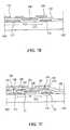
- FIGS. 7A to 7 Care sequential cross-sectional views taken along a line “VII—VII” of FIG. 5 .
- FIG. 5is a schematic plan view of an array substrate for an IPS-LCD device according to an embodiment.
- a pixel region “P”is defined by a row gate line 113 and a column data line 115 .
- a TFT “T” having a gate electrode 121 , an active layer 124 , a source electrode 123 and a drain electrode 125is disposed adjacent to a crossing portion of the gate and data lines 113 and 115 .
- a common line 117 of the same material as the gate line 113is disposed at the pixel region “P” parallel to the gate line 113 .
- the common line 117is spaced apart from the gate line 113 and is disposed in the middle of the (n)-th and (n ⁇ 1)-th gate lines so that the electrical shortage between the common and gate lines 117 and 113 cannot occur.
- the common line 117has a plurality of extended portions 118 and 119 at the boundary of the pixel region “P”, which are elongated nearly perpendicular to the common line 117 and disposed adjacent to the data line 115 as a auxiliary black matrix so that the light leakage between the data line 115 and an extended portion 136 of a common electrode 135 can be prevented.
- a first storage electrode 127 and a second storage electrode 129are disposed over the common line 117 and the gate line 113 , respectively.
- the first and second storage electrodes 127 and 129are connected to the drain electrode 125 through extended lines 126 and 128 so that first and second storage capacitors “C1” and “C2” are formed between the common line 117 and the first storage electrode 127 and between the gate line 113 and the second storage electrode 129 , respectively.
- the pixel region “P”can be divided into first and second regions “M” and “N”.
- a plurality of extended portions 136 of a common electrode 135 and a plurality of extended portions 132 and 134 of first and second pixel electrodes 131 and 133are disposed alternately at the first and second regions “M” and “N”.
- the common electrode 135is connected to the common line 117 through contact holes 145 and 147 and the plurality of extended portions 136 have a substantially zigzag shape and extend nearly perpendicular to the common electrode 135 .
- the first and second pixel electrodes 131 and 133 and their extended portions 132 and 134are independently disposed at the first and second regions “M” and “N”, respectively.
- the first pixel electrode 131 of the first region “M”is connected to the drain electrode 125 and the plurality of extended portions 132 have a substantially zigzag shape and extend nearly perpendicular to the first pixel electrode 131 .
- the second pixel electrode 133 of the second region “N”is connected to the second storage electrode 129 and the plurality of extended portions 134 have a substantially zigzag shape and extend nearly perpendicular to the second pixel electrode 133 . Therefore, the independent first and second pixel electrodes 131 and 133 are connected to the drain electrode 125 and the signal of the data line 115 can be transferred.
- FIGS. 6A to 6 C and 7 A to 7 Care sequential cross-sectional views taken along lines “VI—VI” and “VII—VII” of FIG. 5 , respectively.
- a gate line 113 , a gate electrode 121 , a common line 117 and a plurality of extended portions 118 and 119 (of FIG. 5 ) of the common line 117are formed on a substrate 111 by depositing and patterning one of conductive materials such as aluminum (Al), aluminum alloy, chromium (Cr), molybdenum (Mo) and tungsten (W). Then, a gate insulator 122 of inorganic materials such as silicon nitride (SiNx) and silicon oxide (SiO 2 ) or organic materials such as bezocyclobutene (BCB) and acrylic resin is formed on the entire surface of the substrate 111 .
- conductive materialssuch as aluminum (Al), aluminum alloy, chromium (Cr), molybdenum (Mo) and tungsten (W).
- a gate insulator 122 of inorganic materialssuch as silicon nitride (SiNx) and silicon oxide (SiO 2 ) or organic
- An active layer 124 of intrinsic amorphous silicon (a-Si:H) and an ohmic contact layer 128 of doped amorphous silicon (n+ or p+ a-Si:H)are subsequently formed on the gate insulator 122 over the gate electrode 121 .
- the ohmic contact layer 128can be formed by thinly doping n+ or p+ ions onto the active layer 124 .
- a data line 115 , a source electrode 123 and a drain electrode 125are formed by depositing and patterning one of conductive materials such as aluminum (Al), aluminum alloy, chromium (Cr), molybdenum (Mo) and tungsten (W).
- the source and drain electrodes 123 and 125contact the ohmic contact layer 128 and are spaced apart from each other.
- the source electrode 123extends from the crossing portion of the data line 115 with the gate line 113 .
- a first storage electrode 127 (not shown) and a second storage electrode 129are formed on the gate insulator 122 over the common line 135 and the gate line 113 with specific areas, respectively.
- the first storage electrode 127is connected to the drain electrode 125 through the first drain extended portions 126 at a first region “M” (of FIG. 5 ) and the second storage electrode 129 is connected to the first storage electrode 127 through the second drain extended portions 128 at a second region “N” (of FIG. 5 ). Therefore, the two storage capacitors are formed, i.e., a first storage capacitor “C1” between the common line 117 and the first storage electrode 127 and the second storage capacitor between the gate line 113 and the second storage electrode 129 .
- a passivation layer 130is formed on the entire surface of the substrate 111 by depositing one of organic materials such as benzocyclobutene (BCB) and acrylic resin or inorganic materials such as silicon nitride (SiNx) and silicon oxide (SiO 2 ). Then, a first contact hole 141 exposing the drain electrode 125 , a second contact hole 143 exposing the second storage electrode 129 and third and fourth contact holes 145 and 147 (of FIG. 5 ) exposing the common line 113 are formed.
- a common electrode 135 having a plurality of extended portions 136is formed on the common line 113 and connected to the common line 113 through the third and forth contact holes 145 and 147 (of FIG.
- first and second pixel electrodes 131 and 133 of the same material as the common electrode 135are formed at the first and second regions “M” and “N”, respectively.
- the first pixel electrode 131 having a plurality of extended portions 132is connected to the drain electrode 125 through the first contact hole 141 and the second pixel electrode 133 having a plurality of extended portions 134 is connected to the second storage electrode 129 through the second contact hole 143 .
- some of extended portions 132 and 134are formed over the first and second drain extended portions 126 and 128 .
- the first and second pixel electrodes 131 and 133are independently formed, the same data are transferred to the first and second pixel electrodes 131 and 133 due to the electric connection to the drain electrode 125 .
- each of extended portions 132 , 134 and 136 of the first and second pixel electrodes 131 and 133 and the common electrode 135has a substantially zigzag shape.
- the gate and common linesare spaced apart from each other or the common line is disposed in the middle of two adjacent gate lines, the electric short or leakage current between the gate and common lines can be prevented, and the reliability of the IPS-LCD device can be increased.
- the pixel and common electrodeshave extended portions at first and second pixel regions, the non-display region between the gate and common lines of the related art can be eliminated, and the aperture ratio and the brightness can be increased.
- the common and pixel electrodesare simultaneously formed on the same layer with a uniform distance, the electric field distribution can be uniform, and flicker can be prevented.
- the common and pixel electrodeshave a bent portion (i.e., have a substantially zigzag shape), the multi-domains can be realized, and the color shift can be decreased.
Landscapes
- Physics & Mathematics (AREA)
- Nonlinear Science (AREA)
- Mathematical Physics (AREA)
- Chemical & Material Sciences (AREA)
- Crystallography & Structural Chemistry (AREA)
- General Physics & Mathematics (AREA)
- Optics & Photonics (AREA)
- Geometry (AREA)
- Liquid Crystal (AREA)
- Engineering & Computer Science (AREA)
- Microelectronics & Electronic Packaging (AREA)
Abstract
Description
Claims (13)
Priority Applications (1)
| Application Number | Priority Date | Filing Date | Title |
|---|---|---|---|
| US10/995,223US7405794B2 (en) | 2000-12-29 | 2004-11-24 | Substrate for in-plane switching mode liquid crystal display device with particular common electrodes on two layer levels and method for fabricating the same |
Applications Claiming Priority (2)
| Application Number | Priority Date | Filing Date | Title |
|---|---|---|---|
| KR2000-85006 | 2000-12-29 | ||
| KR1020000085006AKR100587217B1 (en) | 2000-12-29 | 2000-12-29 | Array board for liquid crystal display device of transverse electric field method and manufacturing method |
Related Child Applications (1)
| Application Number | Title | Priority Date | Filing Date |
|---|---|---|---|
| US10/995,223DivisionUS7405794B2 (en) | 2000-12-29 | 2004-11-24 | Substrate for in-plane switching mode liquid crystal display device with particular common electrodes on two layer levels and method for fabricating the same |
Publications (2)
| Publication Number | Publication Date |
|---|---|
| US20020093614A1 US20020093614A1 (en) | 2002-07-18 |
| US6839114B2true US6839114B2 (en) | 2005-01-04 |
Family
ID=19703845
Family Applications (2)
| Application Number | Title | Priority Date | Filing Date |
|---|---|---|---|
| US10/025,902Expired - LifetimeUS6839114B2 (en) | 2000-12-29 | 2001-12-26 | Substrate for in-plane switching mode liquid crystal display device with capacitors connected by extending lines and method for fabricating the same |
| US10/995,223Expired - Fee RelatedUS7405794B2 (en) | 2000-12-29 | 2004-11-24 | Substrate for in-plane switching mode liquid crystal display device with particular common electrodes on two layer levels and method for fabricating the same |
Family Applications After (1)
| Application Number | Title | Priority Date | Filing Date |
|---|---|---|---|
| US10/995,223Expired - Fee RelatedUS7405794B2 (en) | 2000-12-29 | 2004-11-24 | Substrate for in-plane switching mode liquid crystal display device with particular common electrodes on two layer levels and method for fabricating the same |
Country Status (2)
| Country | Link |
|---|---|
| US (2) | US6839114B2 (en) |
| KR (1) | KR100587217B1 (en) |
Cited By (4)
| Publication number | Priority date | Publication date | Assignee | Title |
|---|---|---|---|---|
| US20040239866A1 (en)* | 2003-03-28 | 2004-12-02 | Fujitsu Display Technologies Corporation. | Liquid crystal display device |
| US20050052604A1 (en)* | 2003-09-08 | 2005-03-10 | Kim Woo Hyun | Array substrate for in plane switching mode liquid crystal display device and method for manufacturing the same |
| US20050110931A1 (en)* | 2003-11-04 | 2005-05-26 | Lg.Philips Lcd Co., Ltd. | Thin film transistor substrate using horizontal electric field and fabricating method thereof |
| US20050179846A1 (en)* | 2004-02-16 | 2005-08-18 | Lee Kyung H. | Fringe field switching liquid crystal display |
Families Citing this family (31)
| Publication number | Priority date | Publication date | Assignee | Title |
|---|---|---|---|---|
| KR100748442B1 (en)* | 2001-02-26 | 2007-08-10 | 엘지.필립스 엘시디 주식회사 | Array board for horizontal electric field drive type liquid crystal display device and manufacturing method thereof |
| US6876420B2 (en)* | 2002-06-25 | 2005-04-05 | Lg. Philips Lcd Co., Ltd. | In-plane switching mode liquid crystal display device |
| JP4199501B2 (en)* | 2002-09-13 | 2008-12-17 | Nec液晶テクノロジー株式会社 | Manufacturing method of liquid crystal display device |
| TW594301B (en)* | 2003-04-09 | 2004-06-21 | Chunghwa Picture Tubes Ltd | Method and structure for broadening cholesteric liquid crystals spectrum |
| JP4424925B2 (en)* | 2003-06-05 | 2010-03-03 | 株式会社 日立ディスプレイズ | Display device |
| JP4293867B2 (en)* | 2003-09-05 | 2009-07-08 | 奇美電子股▲ふん▼有限公司 | IPS liquid crystal display corresponding to pixel enlargement |
| KR101157223B1 (en)* | 2003-10-29 | 2012-06-15 | 엘지디스플레이 주식회사 | In plane switching mode liquid crystal display device and fabrication method threrof |
| KR100560404B1 (en)* | 2003-11-04 | 2006-03-14 | 엘지.필립스 엘시디 주식회사 | Horizontal field applied thin film transistor substrate and manufacturing method thereof |
| KR100643039B1 (en)* | 2003-12-11 | 2006-11-10 | 엘지.필립스 엘시디 주식회사 | Transverse electric field type liquid crystal display device |
| CN100483225C (en)* | 2004-05-28 | 2009-04-29 | 鸿富锦精密工业(深圳)有限公司 | Plane internally switched type liquid crystal display device |
| CN100483226C (en)* | 2004-05-28 | 2009-04-29 | 鸿富锦精密工业(深圳)有限公司 | Semi- transmissive liquid crystal display device |
| CN100483227C (en)* | 2004-05-28 | 2009-04-29 | 鸿富锦精密工业(深圳)有限公司 | Reflective liquid crystal display device |
| KR20060001662A (en)* | 2004-06-30 | 2006-01-06 | 엘지.필립스 엘시디 주식회사 | Horizontal field type liquid crystal display device and manufacturing method thereof |
| TWI379113B (en)* | 2004-07-07 | 2012-12-11 | Samsung Display Co Ltd | Array substrate, manufacturing method thereof and display device having the same |
| US20090027328A1 (en)* | 2004-08-23 | 2009-01-29 | Koninklijke Philips Electronics, N.V. | Active matrix devices |
| KR20060131013A (en)* | 2005-06-14 | 2006-12-20 | 비오이 하이디스 테크놀로지 주식회사 | Fringe field switching mode LCD |
| EP1793266B1 (en) | 2005-12-05 | 2017-03-08 | Semiconductor Energy Laboratory Co., Ltd. | Transflective Liquid Crystal Display with a Horizontal Electric Field Configuration |
| KR101229413B1 (en) | 2006-04-18 | 2013-02-04 | 엘지디스플레이 주식회사 | An array substrate for In-Plane switching mode LCD and method of fabricating of the same |
| KR20070109521A (en)* | 2006-05-11 | 2007-11-15 | 삼성전자주식회사 | A thin film transistor substrate, a liquid crystal display panel including the same, and a manufacturing method of the liquid crystal display panel |
| KR100978263B1 (en) | 2006-05-12 | 2010-08-26 | 엘지디스플레이 주식회사 | LCD and its manufacturing method |
| TWI545380B (en)* | 2006-05-16 | 2016-08-11 | 半導體能源研究所股份有限公司 | Liquid crystal display device and semiconductor device |
| US8351006B2 (en)* | 2007-05-14 | 2013-01-08 | Lg Display Co., Ltd. | Liquid crystal display device and fabricating method thereof |
| US8125603B2 (en)* | 2007-05-17 | 2012-02-28 | Lg Display Co., Ltd. | In-plane switching mode liquid crystal display device and method for fabricating the same |
| KR101377007B1 (en)* | 2007-08-14 | 2014-03-26 | 삼성디스플레이 주식회사 | Thin film transistor array substrate and liquid crystal display panel comprising the same |
| KR101443380B1 (en)* | 2007-11-23 | 2014-09-26 | 엘지디스플레이 주식회사 | Liquid crystal display |
| KR101579135B1 (en)* | 2008-12-03 | 2015-12-22 | 삼성디스플레이 주식회사 | Thin film transistor substrate and manufacturing method thereof |
| US8891050B2 (en)* | 2011-12-15 | 2014-11-18 | Lg Display Co., Ltd. | Liquid crystal display device and method for fabricating the same |
| CN103268041B (en)* | 2013-05-17 | 2015-11-25 | 京东方科技集团股份有限公司 | Display panels and driving method thereof |
| CN105242464B (en)* | 2015-11-13 | 2018-07-17 | 武汉华星光电技术有限公司 | A kind of method, the array substrate of liquid crystal display and its response time of raising |
| CN205247020U (en)* | 2015-12-28 | 2016-05-18 | 京东方科技集团股份有限公司 | Display substrate and display device |
| CN117157581A (en)* | 2022-03-31 | 2023-12-01 | 京东方科技集团股份有限公司 | Array substrate, display panel and display device |
Citations (21)
| Publication number | Priority date | Publication date | Assignee | Title |
|---|---|---|---|---|
| JPH095764A (en) | 1995-06-20 | 1997-01-10 | Hitachi Ltd | LCD display substrate |
| US5598285A (en) | 1992-09-18 | 1997-01-28 | Hitachi, Ltd. | Liquid crystal display device |
| JPH0973101A (en) | 1995-09-06 | 1997-03-18 | Hitachi Ltd | Liquid crystal display device and manufacturing method thereof |
| JPH09101538A (en) | 1995-10-04 | 1997-04-15 | Hitachi Ltd | Active matrix type liquid crystal display device and manufacturing method thereof |
| JPH09105908A (en) | 1995-10-09 | 1997-04-22 | Hitachi Ltd | Active matrix type liquid crystal display |
| US5745207A (en)* | 1995-11-30 | 1998-04-28 | Matsushita Electric Industrial Co., Ltd. | Active matrix liquid crystal display having electric fields parallel to substrates |
| US5838037A (en) | 1996-11-15 | 1998-11-17 | Mitsubishi Denki Kabushiki Kaisha | TFT-array and manufacturing method therefor |
| US5946060A (en) | 1996-06-03 | 1999-08-31 | Sharp Kabushiki Kaisha | Liquid crystal display device and method for driving the same |
| KR100218527B1 (en) | 1996-06-26 | 1999-09-01 | 윤종용 | Liquid crystal display device and its manufacturing method of in-plane switching mode |
| US5978059A (en)* | 1995-03-17 | 1999-11-02 | Hitachi, Ltd. | Liquid crystal display device with wide viewing angle characteristics |
| US5977562A (en)* | 1995-11-14 | 1999-11-02 | Semiconductor Energy Laboratory Co., Ltd. | Electro-optical device |
| US5990987A (en) | 1997-11-18 | 1999-11-23 | Nec Corporation | Transverse electrical field LCD with islands having a pattern the same as the combined pattern of gate electrodes, gate bus lines and counter electrodes |
| US6028653A (en) | 1996-06-21 | 2000-02-22 | Nec Corporation | Active matrix liquid crystal display panel having an improved numerical aperture and display reliability and wiring designing method therefor |
| KR100250972B1 (en) | 1996-10-31 | 2000-04-15 | 윤종용 | Liquid crystal display |
| US6097454A (en) | 1996-06-25 | 2000-08-01 | Semiconductor Energy Laboratory Co., Ltd. | Display device |
| US6288763B1 (en)* | 1996-04-16 | 2001-09-11 | Obayashiseikou Co., Ltd. | Liquid crystal display device having comblike bent interdigital electrodes |
| US6300995B1 (en)* | 1996-08-07 | 2001-10-09 | Hitachi, Ltd | Liquid crystal display device utilizing in-plane-switching system and having alignment film separating picture element electrode or counter electrode from liquid crystal layer |
| US20020044249A1 (en)* | 1996-04-16 | 2002-04-18 | Naoto Hirota | Liquid crystal display device |
| US6486934B2 (en)* | 1999-12-24 | 2002-11-26 | Hyundai Display Technology Inc. | Method for manufacturing fringe field switching mode liquid crystal display device |
| US6507383B1 (en)* | 2000-03-21 | 2003-01-14 | Hitachi, Ltd. | In-plane switching liquid crystal display apparatus with reduced capacitance between pixel electrodes and common electrodes |
| US20030063074A1 (en)* | 2000-04-24 | 2003-04-03 | Katsuhiko Kumagawa | Display unit and drive method therefor |
Family Cites Families (2)
| Publication number | Priority date | Publication date | Assignee | Title |
|---|---|---|---|---|
| KR100205522B1 (en)* | 1996-04-08 | 1999-07-01 | 구자홍 | Thin film transistor array substrate and manufacturing method thereof |
| JP4130490B2 (en)* | 1997-10-16 | 2008-08-06 | 三菱電機株式会社 | Liquid crystal display |
- 2000
- 2000-12-29KRKR1020000085006Apatent/KR100587217B1/ennot_activeExpired - Fee Related
- 2001
- 2001-12-26USUS10/025,902patent/US6839114B2/ennot_activeExpired - Lifetime
- 2004
- 2004-11-24USUS10/995,223patent/US7405794B2/ennot_activeExpired - Fee Related
Patent Citations (21)
| Publication number | Priority date | Publication date | Assignee | Title |
|---|---|---|---|---|
| US5598285A (en) | 1992-09-18 | 1997-01-28 | Hitachi, Ltd. | Liquid crystal display device |
| US5978059A (en)* | 1995-03-17 | 1999-11-02 | Hitachi, Ltd. | Liquid crystal display device with wide viewing angle characteristics |
| JPH095764A (en) | 1995-06-20 | 1997-01-10 | Hitachi Ltd | LCD display substrate |
| JPH0973101A (en) | 1995-09-06 | 1997-03-18 | Hitachi Ltd | Liquid crystal display device and manufacturing method thereof |
| JPH09101538A (en) | 1995-10-04 | 1997-04-15 | Hitachi Ltd | Active matrix type liquid crystal display device and manufacturing method thereof |
| JPH09105908A (en) | 1995-10-09 | 1997-04-22 | Hitachi Ltd | Active matrix type liquid crystal display |
| US5977562A (en)* | 1995-11-14 | 1999-11-02 | Semiconductor Energy Laboratory Co., Ltd. | Electro-optical device |
| US5745207A (en)* | 1995-11-30 | 1998-04-28 | Matsushita Electric Industrial Co., Ltd. | Active matrix liquid crystal display having electric fields parallel to substrates |
| US20020044249A1 (en)* | 1996-04-16 | 2002-04-18 | Naoto Hirota | Liquid crystal display device |
| US6288763B1 (en)* | 1996-04-16 | 2001-09-11 | Obayashiseikou Co., Ltd. | Liquid crystal display device having comblike bent interdigital electrodes |
| US5946060A (en) | 1996-06-03 | 1999-08-31 | Sharp Kabushiki Kaisha | Liquid crystal display device and method for driving the same |
| US6028653A (en) | 1996-06-21 | 2000-02-22 | Nec Corporation | Active matrix liquid crystal display panel having an improved numerical aperture and display reliability and wiring designing method therefor |
| US6097454A (en) | 1996-06-25 | 2000-08-01 | Semiconductor Energy Laboratory Co., Ltd. | Display device |
| KR100218527B1 (en) | 1996-06-26 | 1999-09-01 | 윤종용 | Liquid crystal display device and its manufacturing method of in-plane switching mode |
| US6300995B1 (en)* | 1996-08-07 | 2001-10-09 | Hitachi, Ltd | Liquid crystal display device utilizing in-plane-switching system and having alignment film separating picture element electrode or counter electrode from liquid crystal layer |
| KR100250972B1 (en) | 1996-10-31 | 2000-04-15 | 윤종용 | Liquid crystal display |
| US5838037A (en) | 1996-11-15 | 1998-11-17 | Mitsubishi Denki Kabushiki Kaisha | TFT-array and manufacturing method therefor |
| US5990987A (en) | 1997-11-18 | 1999-11-23 | Nec Corporation | Transverse electrical field LCD with islands having a pattern the same as the combined pattern of gate electrodes, gate bus lines and counter electrodes |
| US6486934B2 (en)* | 1999-12-24 | 2002-11-26 | Hyundai Display Technology Inc. | Method for manufacturing fringe field switching mode liquid crystal display device |
| US6507383B1 (en)* | 2000-03-21 | 2003-01-14 | Hitachi, Ltd. | In-plane switching liquid crystal display apparatus with reduced capacitance between pixel electrodes and common electrodes |
| US20030063074A1 (en)* | 2000-04-24 | 2003-04-03 | Katsuhiko Kumagawa | Display unit and drive method therefor |
Non-Patent Citations (6)
| Title |
|---|
| H. Wakemoto et al.; "An Advanced In-Plane Switching Mode TFT-LCD"; SID 97 Digest; pp. 929-932. |
| M. Oh-e, et al.; "Principles and Characteristics of Electro-Optical Behaviour with In-Plane Switching Mode"; Asis Display '95; pp. 557-580. |
| M. Ohta et al.; "Development of Super-TFT-LCDs with In-Plane Switching Display Mode"; Asia Display '95; pp. 707-710. |
| R. Kieler et al.; "In-Plane Switching of Nematic Liquid Crystals"; Japan Display '92; pp. 547-550. |
| S. Matsumoto et al.; Display Characteristics of In-Plane Switching (IPS) LCDs and a Wide-Viewing-Angle 14.5-in. OPS TFT-LCD; Euro Display '96; pp. 445-448. |
| S.H. Lee et al.; High-Transmittance, Wide-Viewing-Angle Nematic Liquid Crystal Display Controlled by Fringe-Field Switching; Asia Display '98; pp. 371-374. |
Cited By (7)
| Publication number | Priority date | Publication date | Assignee | Title |
|---|---|---|---|---|
| US20040239866A1 (en)* | 2003-03-28 | 2004-12-02 | Fujitsu Display Technologies Corporation. | Liquid crystal display device |
| US20050052604A1 (en)* | 2003-09-08 | 2005-03-10 | Kim Woo Hyun | Array substrate for in plane switching mode liquid crystal display device and method for manufacturing the same |
| US7277149B2 (en)* | 2003-09-08 | 2007-10-02 | Lg.Philips Lcd Co., Ltd. | Array substrate for in plane switching mode liquid crystal display device and method for manufacturing the same |
| US20050110931A1 (en)* | 2003-11-04 | 2005-05-26 | Lg.Philips Lcd Co., Ltd. | Thin film transistor substrate using horizontal electric field and fabricating method thereof |
| US7576822B2 (en)* | 2003-11-04 | 2009-08-18 | Lg Display Co., Ltd. | Thin film transistor substrate using horizontal electric field and fabricating method thereof |
| US20050179846A1 (en)* | 2004-02-16 | 2005-08-18 | Lee Kyung H. | Fringe field switching liquid crystal display |
| US7145621B2 (en)* | 2004-02-16 | 2006-12-05 | Boe Hydis Technology Co., Ltd. | Fringe field switching liquid crystal display having sawtooth edges on the common and pixel electrodes and on the conductive black matrix |
Also Published As
| Publication number | Publication date |
|---|---|
| US20020093614A1 (en) | 2002-07-18 |
| KR100587217B1 (en) | 2006-06-08 |
| US20050099569A1 (en) | 2005-05-12 |
| KR20020055784A (en) | 2002-07-10 |
| US7405794B2 (en) | 2008-07-29 |
Similar Documents
| Publication | Publication Date | Title |
|---|---|---|
| US6839114B2 (en) | Substrate for in-plane switching mode liquid crystal display device with capacitors connected by extending lines and method for fabricating the same | |
| US6784965B2 (en) | In-plane switching mode liquid crystal display device and manufacturing method thereof | |
| US6661492B2 (en) | In-plane switching LCD device | |
| US6710836B2 (en) | Array substrate for in-plane switching mode liquid crystal display device and manufacturing method thereof | |
| US7916258B2 (en) | In-plane switching LCD panel | |
| US6459465B1 (en) | Liquid crystal panel for IPS mode liquid crystal display device and method for fabricating the same | |
| US7342252B2 (en) | Thin film transistor array substrate and fabricating method thereof | |
| US6724454B2 (en) | Ips lcd device having a light shielding layer under at least one common or data electrodes so that light transmittance areas of the common and data electrodes are the same and a method of manufacturing the same | |
| US6911668B2 (en) | Array substrate for in-plane switching mode liquid crystal display device | |
| US7551257B2 (en) | In-plane switching mode liquid crystal display device and method of fabricating the same | |
| US7751009B2 (en) | Array substrate for in-plane switching mode liquid crystal display | |
| US20030043329A1 (en) | Array substrate for in-plane switching liquid crystal display device and manufacturing method of the same | |
| US6657694B2 (en) | In-plane switching LCD device having slanted corner portions | |
| US6583841B2 (en) | In-Plane switching LCD panel wherein pixel electrodes and common electrodes having plurality of first tips and second tips respectively | |
| US7180563B2 (en) | Array substrate and fabrication method for in-plane switching mode liquid crystal display device having pixel electrode overlapping common line and adjacent gate line | |
| US7289180B2 (en) | Liquid crystal display device of a horizontal electric field applying type comprising a storage capacitor substantially parallel to the data line and fabricating method thereof | |
| KR19980031798A (en) | Planar drive type liquid crystal display device and manufacturing method thereof | |
| US7006187B2 (en) | Array substrate for in-plane switching mode liquid crystal display device and method of fabricating the same |
Legal Events
| Date | Code | Title | Description |
|---|---|---|---|
| AS | Assignment | Owner name:LG.PHILIPS LCD CO., LTD., KOREA, REPUBLIC OF Free format text:ASSIGNMENT OF ASSIGNORS INTEREST;ASSIGNORS:MOON, HONG-MAN;PARK, SANG-CHOL;CHUNG, JAE-YOUNG;REEL/FRAME:012406/0491 Effective date:20011226 | |
| AS | Assignment | Owner name:LG.PHILIPS LCD CO., LTD., KOREA, REPUBLIC OF Free format text:CORRECTIVE ASSIGNMENT TO CORRECT THE EXECUTION DATE PREVIOUSLY RECORDED AT REEL 012406, FRAME 0491;ASSIGNORS:PARK, SANG-CHOL;CHUNG, JAE-YOUNG;REEL/FRAME:012739/0440;SIGNING DATES FROM 20020306 TO 20020312 | |
| STCF | Information on status: patent grant | Free format text:PATENTED CASE | |
| FPAY | Fee payment | Year of fee payment:4 | |
| AS | Assignment | Owner name:LG DISPLAY CO., LTD., KOREA, REPUBLIC OF Free format text:CHANGE OF NAME;ASSIGNOR:LG.PHILIPS LCD CO., LTD.;REEL/FRAME:021763/0177 Effective date:20080304 Owner name:LG DISPLAY CO., LTD.,KOREA, REPUBLIC OF Free format text:CHANGE OF NAME;ASSIGNOR:LG.PHILIPS LCD CO., LTD.;REEL/FRAME:021763/0177 Effective date:20080304 | |
| FEPP | Fee payment procedure | Free format text:PAYOR NUMBER ASSIGNED (ORIGINAL EVENT CODE: ASPN); ENTITY STATUS OF PATENT OWNER: LARGE ENTITY Free format text:PAYER NUMBER DE-ASSIGNED (ORIGINAL EVENT CODE: RMPN); ENTITY STATUS OF PATENT OWNER: LARGE ENTITY | |
| FPAY | Fee payment | Year of fee payment:8 | |
| FPAY | Fee payment | Year of fee payment:12 |