US6839104B2 - Common electrode substrate and liquid crystal display device having the same - Google Patents
Common electrode substrate and liquid crystal display device having the sameDownload PDFInfo
- Publication number
- US6839104B2 US6839104B2US09/923,076US92307601AUS6839104B2US 6839104 B2US6839104 B2US 6839104B2US 92307601 AUS92307601 AUS 92307601AUS 6839104 B2US6839104 B2US 6839104B2
- Authority
- US
- United States
- Prior art keywords
- common electrode
- regions
- liquid crystal
- pixel
- pixel electrodes
- Prior art date
- Legal status (The legal status is an assumption and is not a legal conclusion. Google has not performed a legal analysis and makes no representation as to the accuracy of the status listed.)
- Expired - Lifetime, expires
Links
Images


Classifications
- G—PHYSICS
- G02—OPTICS
- G02F—OPTICAL DEVICES OR ARRANGEMENTS FOR THE CONTROL OF LIGHT BY MODIFICATION OF THE OPTICAL PROPERTIES OF THE MEDIA OF THE ELEMENTS INVOLVED THEREIN; NON-LINEAR OPTICS; FREQUENCY-CHANGING OF LIGHT; OPTICAL LOGIC ELEMENTS; OPTICAL ANALOGUE/DIGITAL CONVERTERS
- G02F1/00—Devices or arrangements for the control of the intensity, colour, phase, polarisation or direction of light arriving from an independent light source, e.g. switching, gating or modulating; Non-linear optics
- G02F1/01—Devices or arrangements for the control of the intensity, colour, phase, polarisation or direction of light arriving from an independent light source, e.g. switching, gating or modulating; Non-linear optics for the control of the intensity, phase, polarisation or colour
- G02F1/13—Devices or arrangements for the control of the intensity, colour, phase, polarisation or direction of light arriving from an independent light source, e.g. switching, gating or modulating; Non-linear optics for the control of the intensity, phase, polarisation or colour based on liquid crystals, e.g. single liquid crystal display cells
- G02F1/133—Constructional arrangements; Operation of liquid crystal cells; Circuit arrangements
- G02F1/1333—Constructional arrangements; Manufacturing methods
- G02F1/1337—Surface-induced orientation of the liquid crystal molecules, e.g. by alignment layers
- G02F1/133707—Structures for producing distorted electric fields, e.g. bumps, protrusions, recesses, slits in pixel electrodes
- G—PHYSICS
- G02—OPTICS
- G02F—OPTICAL DEVICES OR ARRANGEMENTS FOR THE CONTROL OF LIGHT BY MODIFICATION OF THE OPTICAL PROPERTIES OF THE MEDIA OF THE ELEMENTS INVOLVED THEREIN; NON-LINEAR OPTICS; FREQUENCY-CHANGING OF LIGHT; OPTICAL LOGIC ELEMENTS; OPTICAL ANALOGUE/DIGITAL CONVERTERS
- G02F1/00—Devices or arrangements for the control of the intensity, colour, phase, polarisation or direction of light arriving from an independent light source, e.g. switching, gating or modulating; Non-linear optics
- G02F1/01—Devices or arrangements for the control of the intensity, colour, phase, polarisation or direction of light arriving from an independent light source, e.g. switching, gating or modulating; Non-linear optics for the control of the intensity, phase, polarisation or colour
- G02F1/13—Devices or arrangements for the control of the intensity, colour, phase, polarisation or direction of light arriving from an independent light source, e.g. switching, gating or modulating; Non-linear optics for the control of the intensity, phase, polarisation or colour based on liquid crystals, e.g. single liquid crystal display cells
- G02F1/137—Devices or arrangements for the control of the intensity, colour, phase, polarisation or direction of light arriving from an independent light source, e.g. switching, gating or modulating; Non-linear optics for the control of the intensity, phase, polarisation or colour based on liquid crystals, e.g. single liquid crystal display cells characterised by the electro-optical or magneto-optical effect, e.g. field-induced phase transition, orientation effect, guest-host interaction or dynamic scattering
- G02F1/139—Devices or arrangements for the control of the intensity, colour, phase, polarisation or direction of light arriving from an independent light source, e.g. switching, gating or modulating; Non-linear optics for the control of the intensity, phase, polarisation or colour based on liquid crystals, e.g. single liquid crystal display cells characterised by the electro-optical or magneto-optical effect, e.g. field-induced phase transition, orientation effect, guest-host interaction or dynamic scattering based on orientation effects in which the liquid crystal remains transparent
- G02F1/1393—Devices or arrangements for the control of the intensity, colour, phase, polarisation or direction of light arriving from an independent light source, e.g. switching, gating or modulating; Non-linear optics for the control of the intensity, phase, polarisation or colour based on liquid crystals, e.g. single liquid crystal display cells characterised by the electro-optical or magneto-optical effect, e.g. field-induced phase transition, orientation effect, guest-host interaction or dynamic scattering based on orientation effects in which the liquid crystal remains transparent the birefringence of the liquid crystal being electrically controlled, e.g. ECB-, DAP-, HAN-, PI-LC cells
- G—PHYSICS
- G02—OPTICS
- G02F—OPTICAL DEVICES OR ARRANGEMENTS FOR THE CONTROL OF LIGHT BY MODIFICATION OF THE OPTICAL PROPERTIES OF THE MEDIA OF THE ELEMENTS INVOLVED THEREIN; NON-LINEAR OPTICS; FREQUENCY-CHANGING OF LIGHT; OPTICAL LOGIC ELEMENTS; OPTICAL ANALOGUE/DIGITAL CONVERTERS
- G02F1/00—Devices or arrangements for the control of the intensity, colour, phase, polarisation or direction of light arriving from an independent light source, e.g. switching, gating or modulating; Non-linear optics
- G02F1/01—Devices or arrangements for the control of the intensity, colour, phase, polarisation or direction of light arriving from an independent light source, e.g. switching, gating or modulating; Non-linear optics for the control of the intensity, phase, polarisation or colour
- G02F1/13—Devices or arrangements for the control of the intensity, colour, phase, polarisation or direction of light arriving from an independent light source, e.g. switching, gating or modulating; Non-linear optics for the control of the intensity, phase, polarisation or colour based on liquid crystals, e.g. single liquid crystal display cells
- G02F1/133—Constructional arrangements; Operation of liquid crystal cells; Circuit arrangements
- G02F1/1333—Constructional arrangements; Manufacturing methods
- G02F1/1335—Structural association of cells with optical devices, e.g. polarisers or reflectors
- G02F1/133509—Filters, e.g. light shielding masks
- G02F1/133512—Light shielding layers, e.g. black matrix
Definitions
- the present inventionrelates to a common electrode substrate that is opposed to an array substrate as well as to a liquid crystal display device having the substrate.
- Liquid crystal display deviceshave a liquid crystal that is sealed between a pair of substrates. Each of the paired substrates has at least one electrode and an alignment film.
- TN (twisted nematic) mode liquid crystal display deviceswhich are widely used conventionally, have horizontal alignment films and a liquid crystal having positive dielectric anisotropy. Liquid crystal molecules are aligned approximately parallel with the horizontal alignment film when a voltage is applied. Liquid crystal molecules rise so as to become approximately perpendicular to the horizontal alignment film when a voltage is applied to those.
- TN mode liquid crystal display deviceshave such advantages that they can be made thin, they have a first disadvantage of a narrow viewing angle and a second disadvantage of low contrast.
- a method for solving the first disadvantage and obtaining a wide viewing angleis domain division.
- each pixelis divided into two domains. In one domain, liquid crystal molecules rise or fall toward one side. In the other domain, liquid crystal molecules rise or fall toward the other side.
- the domainshaving different view angle characteristics in each pixel, the view angle characteristic of the device as a whole is averaged, and a wide viewing angle can thereby be obtained.
- a usual method for controlling the alignment of a liquid crystalis to rub an alignment film.
- rubbingis performed in a first direction in one domain of each pixel by using a mask, and then, rubbing is performed in a second direction that is opposite to the first direction in the other domain by using a complementary mask.
- the entire alignment filmis rubbed in a first direction, and then, one domain or the other domain of each pixel is selectively irradiated with ultraviolet light by using a mask to produce a difference in the pre-tilt of liquid crystal molecules between the one domain and the other domain.
- Rubbingneeds to be performed in liquid crystal display devices having horizontal alignment films. Failures due to pollution and static electricity that occur during the rubbing are factors of lowering the yield.
- VA (vertically aligned) mode liquid crystal display devices having vertical alignment filmsliquid crystal molecules are aligned approximately perpendicular to the vertical alignment films when no voltage is applied. Liquid crystal molecules fall so as to become parallel with the vertical alignment films when a voltage is applied.
- Thisprovides high contrast and solves the second disadvantage (low contrast) of the TN mode liquid crystal display devices.
- the alignment filmsare usually rubbed to control, the liquid crystal alignment.
- Japanese Patent Application No. 185836/1998 of the present applicantproposes a liquid crystal display device in which the liquid crystal alignment can be controlled without rubbing.
- This liquid crystal display deviceis a VA mode liquid crystal display device having vertical alignment films and negative dielectric anisotropy.
- linear alignment regulating structuresprotrusions or slits
- VA mode liquid crystal display devicethis type of VA mode liquid crystal display device will be hereinafter referred to as “MVA (multi-domain vertical alignment) liquid crystal display device.”
- the MVA liquid crystal display devicehas advantages that the rubbing is not necessary and domain division can be attained by arranging linear alignment regulating structures. Therefore, the MVA liquid crystal display device can provide a wide viewing angle and high contrast. Since the rubbing is not necessary, the liquid crystal display device can be manufactured easily and is free of pollution due to dust, etc. that would otherwise be scraped off alignment films during rubbing, leading to an increase of the reliability of the liquid crystal display device.
- FIG. 21is a plan view showing the basic configuration of a conventional MVA liquid crystal display device and shows one pixel and a region in its vicinity.
- This MVA liquid crystal display deviceis an active matrix type liquid crystal display device in which each pixel is provided with a thin-film transistor (TFT) 102 as a switching element.
- TFTthin-film transistor
- Gate bus lines 104 extending in the right-left direction in FIG. 21 and drain bus lines 106 extending in the top-bottom direction in FIG. 21are formed on an array substrate 122 that is provided with the TFTs 102 .
- Each TFT 102is constructed of a drain electrode 108 that extends from the drain bus line 106 , a source electrode 110 that is opposed to the drain electrode 108 , and a portion (gate electrode) of the gate bus line 104 which overlaps with the drain electrode 108 and the source electrode 110 .
- channel layers made of, for example, an amorphous silicon ( ⁇ -Si) film,are formed on the respective gate bus lines 104 .
- the pixel electrodes 112 that are connected to the respective source electrodes 110are further formed on the array substrate 122 .
- Each pixel electrode 112is provided with slits 114 that are oblique with respect to the edges of the pixel electrode 112 .
- the slits 114are alignment regulating structures on the array substrate 122 side for controlling the liquid crystal alignment.
- Each pixel electrode 112is provided with connecting portions 116 so as not to be separated electrically by the slits 114 . Thus, the pixel electrode 112 in each pixel is electrically connected.
- a common electrode substrate 128that is provided with a common electrode and color filters (both not shown in FIG. 21 ) is formed a light shield film 136 (indicated by hatching in the top-left-to-bottom-right direction) in the regions where the TFTs 102 on the array substrate 122 are formed and other regions where neither the pixel electrodes 112 nor the alignment regulating structures (slits 114 in FIG. 21 ) are formed.
- the light shield film 136is formed to suppress leak current that is caused by light incident on the channel layer of each TFT 102 , prevent leakage of light from the adjacent pixel electrodes 112 , and prevent color mixing between the adjacent pixels.
- the light shield film 136is formed in such a manner that the edges approximately coincide with the edges of the pixel electrodes 112 when viewed in the direction perpendicular to the surfaces of the common electrode substrate 128 .
- protrusions 118are the alignment regulating structures together with the slits 114 that are formed on the opposite array substrate 122 .
- each pixelmeasures 99 ⁇ m ⁇ 297 ⁇ m.
- the width of the slits 114 and the protrusions 118is 10 ⁇ m, and the interval between the slits 114 and the protrusions 118 is 25 ⁇ m when viewed in the direction parallel with the substrate surfaces.
- the width of the connecting portions 116 of the pixel electrodes 112is 4 ⁇ m, and the distance between the end portions of the drain bus lines 106 and the edges of the pixel electrodes 112 is 7 ⁇ m.
- FIGS. 22 to 24which are simplified sectional views taken along line E—E in FIG. 21 , show functions of the slits 114 and the protrusions 118 that are the alignment regulating structures for controlling the liquid crystal alignment.
- FIG. 22shows a state of the liquid crystal when no voltage is applied between the pair of substrates 122 and 128 .
- the pixel electrodes 112are formed on a glass substrate 120
- the slits 114are formed on the pixel electrode 112 .
- an alignment film (vertical alignment film) 126is formed so as to cover the pixel electrodes 112 and the slits 114 .
- the common electrode 124is formed on the entire surface of the glass substrate 120 so as to be opposed to the pixel electrodes 112 .
- the protrusions 118 made of an insulator (dielectric) such as a resistare formed on the common electrode 124 .
- an alignment film 126is formed so as to cover the common electrode 124 and the protrusions 118 .
- a liquid crystal LCis sealed between the array substrate 122 and the common electrode substrate 128 .
- Liquid crystal molecules(indicated by ellipses in FIG. 22 ) are aligned perpendicular to the alignment films 126 . Therefore, the liquid crystal molecules are also aligned perpendicular to the alignment films 126 which are formed on the surfaces of the protrusions 118 , and the liquid crystal molecules in the vicinity of the surfaces of the protrusions 118 are inclined against the glass substrate 120 . However, strictly, the liquid crystal molecules in the vicinity of the protrusions 118 are not aligned perpendicular to the alignment films 126 .
- the liquid crystal moleculesare aligned approximately perpendicular to the glass substrates 120 by the alignment films 126 . Because of the continuity of the liquid crystal, the liquid crystal molecules in the vicinity of the surface of each protrusion 118 follow the liquid crystal molecules located in the major part of the pixel, and hence, are inclined from the direction perpendicular to the alignment film 126 toward the normal to the glass substrate 120 . Although not shown in FIG. 22 , a pair of polarizers are disposed outside the glass substrates 120 of the array substrate 122 and of the common electrode substrate 128 in the crossed Nicols state. Therefore, black display is obtained when no voltage is applied.
- FIG. 23shows equipotential lines when voltages are applied between the electrodes of the pair of substrates.
- FIG. 24shows a state of the liquid crystal in this condition.
- equipotential linesdashed lines in FIG. 23
- electric field distributions in the regions where the slits 114 or the protrusions 118 are formeddiffer from those in the other regions.
- the liquid crystal molecules in the vicinity of each protrusion 118fall in two directions that are approximately perpendicular to the direction where the protrusion 118 is provided, with the protrusion 118 being as the boundary. Since liquid crystal molecules in the vicinity of each protrusion 118 are slightly inclined from the direction perpendicular to the glass substrate 120 even when no voltage is applied, they fall quickly in response to the electric field. Nearby the liquid crystal molecules also fall quickly following the behavior of the liquid crystal molecules in the vicinity of the protrusion 118 while being influenced by the electric field. Similarly, where the slits 114 are provided in a linear state as shown in FIG. 21 , the liquid crystal molecules in the vicinity of each slit 114 fall in two directions that are approximately perpendicular to the direction where the slit 114 is provided, with the slit 114 being as the boundary.
- the liquid crystal moleculesfall in the same direction, that is, they are aligned in the same direction.
- symbols [A] to [D] in FIG. 21 in a typified mannerin the MVA liquid crystal display device, the four regions having different alignment directions are formed in each pixel, whereby a feature of a wide viewing angle is obtained.
- the above alignment control using the alignment regulating structuresis not limited to the case of the combinations of the slits 114 and the protrusions 118 shown in FIGS. 21 to 24 ; a similar alignment control can be performed by using, as the alignment regulating structures, the combination of protrusions and protrusions or the combination of slits and slits.
- the MVA liquid crystal display deviceprovides a wide viewing angle, it had a problem that there exist regions where the alignment of liquid crystal molecules is not stable, resulting in lowering the luminance. That is, when voltages are applied between the electrodes, alignment defective regions 130 occur as hatched in FIG. 21 .
- the alignment defective regions 130where the light transmittance is low, are a factor of lowering the luminance in white display.
- the alignment defective regions 130occur along the drain bus lines 106 on the side where the alignment regulating structures (protrusions 118 in FIG. 21 ) that are provided on the common electrode substrate 128 form obtuse angles with the edges of each pixel electrode 112 when viewed in the direction perpendicular to the substrate surfaces.
- the liquid crystal moleculeshave different alignment directions from the alignment directions that are controlled by the alignment regulating structures (protrusions 118 and slits 114 in FIG. 21 ) that are provided in the pair of substrates.
- FIG. 25is a plan view showing an MVA liquid crystal display device that solves the above problem and, more specifically, shows one pixel and a region in its vicinity.
- the components in FIG. 25 having the same functions as the corresponding components in FIG. 21are given the same reference symbols as the latter and will not be described below.
- the MVA liquid crystal display device of FIG. 25has auxiliary protrusions 132 that are alignment regulating structures for performing a strong alignment control in the alignment defective regions 130 shown in FIG. 21 .
- the auxiliary protrusions 132branch off the protrusions 118 and are formed along the end portions of each pixel electrode 112 , that is, the drain bus lines 106 .
- liquid crystal molecules (indicated by cylinders in FIG. 25 ) aare aligned continuously with liquid crystal molecules b, whereby the alignment of liquid crystal molecules is made stable in the alignment defective regions 130 .
- FIG. 26shows a display area in which a band-like black figure that is long in the top-bottom direction in FIG. 26 (hereinafter referred to as “black vertical band”) is displayed against a white background on the conventional MVA liquid crystal display device of FIG. 25 .
- black vertical banda band-like black figure that is long in the top-bottom direction in FIG. 26
- pixel Athat is part of the background
- pixel B in the black vertical banddisplays black.
- pixel Cthat is located under the black vertical band in FIG. 26 displays white, it is darker than pixel A.
- Pixel Cbecomes more darker than pixel A as the black vertical band becomes longer in the vertical direction in FIG. 26 .
- the conventional MVA liquid crystal display device of FIG. 25has the problem that when a black vertical band is displayed against a white background, a region displaying white under the black vertical band is displayed darker than the other region displaying white.
- FIG. 27shows a display area in which a band-like white figure that is long in the top-bottom direction in FIG. 26 (hereinafter referred to as “white vertical band”) is displayed against a black background on the conventional MVA liquid crystal display device of FIG. 25 .
- white vertical banda band-like white figure that is long in the top-bottom direction in FIG. 26
- pixel Athat is part of the background displays black
- pixel B in the white vertical banddisplays white.
- pixel Cthat is located under the white vertical band in FIG. 26 displays black, it is brighter than pixel A.
- Pixel Cbecomes more brighter than pixel A as the white vertical band becomes longer in the vertical direction in FIG. 26 .
- the vertical crosstalkoccurs in such a manner that horizontal electric fields that develop between the drain bus lines 106 and end portions of each pixel electrode 112 where the auxiliary protrusions 132 are not formed influence the alignment of liquid crystal molecules.
- An object of the present inventionis to provide a common electrode substrate capable of providing high luminance and good display characteristics as well as a liquid crystal display device having such a common electrode substrate.
- a common electrode substratecomprising a transparent insulating substrate to be arranged opposite to an array substrate having pixel electrodes formed in respective pixel regions that are defined by a plurality of gate bus lines and drain bus lines, and to hold a liquid crystal having negative dielectric anisotropy; a common electrode formed on the transparent insulating substrate; alignment regulating structures having linear protrusions formed on the common electrode; and a light shield film formed on the transparent insulating substrate and having overlap regions that overlap the pixel electrodes when viewed in the direction perpendicular to the surface of the transparent insulating substrate so as to shield, from light, alignment defective regions of the liquid crystal formed in regions of end portions of the pixel electrodes.
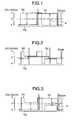
- FIGS. 1 to 3are graphs for description of the main reason for vertical crosstalk that occurs in a conventional liquid crystal display device as a basis of a first embodiment of the present invention
- FIGS. 4 and 5are schematic sectional views for description of the main reason for the vertical crosstalk that occurs in the conventional liquid crystal display device as a basis of the first embodiment of the invention
- FIG. 6is a plan view showing the configuration of the conventional liquid crystal display device as a basis of the first embodiment of the invention.
- FIGS. 7 to 9are graphs for description of the main reason for vertical crosstalk that occurs in the conventional liquid crystal display device as a basis of a first embodiment of the present invention.
- FIGS. 10 and 11are schematic sectional views for description of the main reason for the vertical crosstalk that occurs in the conventional liquid crystal display device as a basis of the first embodiment of the invention
- FIG. 12shows the entire configuration of a liquid crystal display device according to the first embodiment of the invention
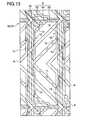
- FIG. 13is a plan view showing a common electrode substrate according to the first embodiment of the invention.
- FIG. 14is a graph showing a relationship between the effect and the overlap width of overlap regions of a light shield film as measured from the end portions of a pixel electrode;
- FIG. 15is a graph showing a relationship between the panel transmittance and the overlap width of the overlap regions of the light shield film as measured from the edges of the pixel electrode;
- FIG. 16is a plan view showing a common electrode substrate according to a modification of the first embodiment of the invention.
- FIGS. 17 and 18are schematic sectional views showing the common electrode substrate according to the modification of the first embodiment
- FIG. 19is a plan view showing a common electrode substrate according to a second embodiment of the invention.
- FIG. 20is a schematic sectional view showing the common electrode substrate according to the second embodiment of the invention.
- FIG. 21is a plan view showing the configuration of a conventional liquid crystal display device
- FIGS. 22 to 24are schematic sectional views showing the configuration of the conventional liquid crystal display device of FIG. 21 ;
- FIG. 25is a plan view showing the configuration of another conventional liquid crystal display device.
- FIGS. 26 and 27illustrate a problem of the conventional liquid crystal display device of FIG. 25 .
- FIGS. 1 to 3are graphs showing examples of a gate voltage, a drain voltage, a pixel voltage, and a common voltage in pixels A, B, and C shown in FIG. 26 , respectively.
- FIG. 1shows a gate voltage V g , a drain voltage V d , a pixel voltage V p , and a common voltage V com in pixel A.
- the abscissarepresents the time and covers about two frames (e.g., about ⁇ fraction (1/30) ⁇ sec) in FIG. 1 .
- the ordinaterepresents the voltage (V).
- Vthe voltage
- the drain voltage V dbecomes +5 V or ⁇ 5 V every frame cycle.
- the gate voltage V gis applied to the gate electrode
- +5 V or ⁇ 5 V of the drain voltage V dis written to pixel A as the pixel voltage V p .
- the pixel voltage V pis held until the next frame by a storage capacitor (not shown).
- the common voltage V comis always equal to 0 V.
- the potential difference e between the pixel voltage V p and the drain voltage V dis equal to 10 V in most of each frame period.
- FIG. 2shows a gate voltage V g , a drain voltage V d , a pixel voltage V p , and a common voltage V com , in pixel B shown in FIG. 26 .
- the abscissa of FIG. 2which represents the time, is the same as that of FIG. 1 and covers about two frames.
- the ordinaterepresents the voltage (V).
- Pixel Bdisplays black, and in FIG. 26 most of the pixels on the drain bus line including pixel B also display black. Therefore, the drain voltage V d is equal to +1 V or ⁇ 1 V in most of each frame period and is equal to +5 V or ⁇ 5 V in the other periods.
- the gate voltage V gis applied to the gate electrode, +1 V or ⁇ 1 V of the drain voltage V d is written to pixel B as the pixel voltage V p .
- FIG. 3shows a gate voltage V g , a drain voltage V d , a pixel voltage V p , and a common voltage V com in pixel C shown in FIG. 26 .
- the abscissa of FIG. 3represents the time and covers about two frames as in the cases of FIGS. 1 and 2 .
- the ordinaterepresents the voltage (V).
- pixel Cdisplays white
- the drain voltage V dis equal to +1 V or ⁇ 1 V in most of each frame period and is equal to +5 V or ⁇ 5 V in the other periods.
- the period when the drain voltage V d is equal to +1 V or ⁇ 1 Vincreases in proportion to the vertical length of the black vertical band.
- the gate voltage V gis applied to the gate electrode, +5 V or ⁇ 5 V of the drain voltage V d is written to pixel C as the pixel voltage V p .
- the potential difference e between the pixel voltage V p and the drain voltage V dis equal to 6 V in most of each frame period and is equal to 10 V in other periods.
- the actual potential difference e between the pixel electrode and the drain bus lineis equal to an average value of them.
- the actual potential difference eis approximately equal to 6 V if the vertical length of the black vertical band is long.
- FIG. 4is a schematic sectional view of an end portion of a pixel electrode 16 of pixel A along a drain bus line 42 .
- An array substrate 32has the drain bus line 42 and the pixel electrode 16 on a glass substrate 22 .
- a common electrode 34 that is opposed to the array substrate 32has a light shield film 6 that is generally formed in a region where the pixel electrode 16 is not formed, and a common electrode 24 that is formed on the almost entire surface of the substrate.
- Vertical alignment films(not shown) for orienting liquid crystal molecules perpendicular to the two substrates 32 and 34 when no voltage is applied are formed on the opposite surfaces of the two substrates 32 and 34 , respectively.
- a liquid crystal LC having negative dielectric anisotropyis sealed between the two substrates 32 and 34 .
- Many of the liquid crystal moleculesare inclined rightward in FIG. 4 by the electric field between the pixel electrodes 16 and the common electrode 24 , whereby a white display is obtained in pixel A.
- the drain voltage V d of the drain bus line 42becomes +5 V or ⁇ 5 V every frame cycle, and the pixel voltage V p of the pixel electrode 16 is equal to ⁇ 5 V or +5 V.
- the common voltage V com of the common electrode 24is equal to 0 V. Therefore, the potential difference between the pixel electrode 16 and the drain bus line 42 is approximately equal to 10 V, and the potential difference between the pixel electrode 16 and the common electrode 24 is equal to 5 V.
- Broken lines in FIG. 4indicate electric fields E 1 and E 2 that develop between the electrodes, and a relationship
- the liquid crystal molecules between the pixel electrode 16 and the drain bus line 42are aligned approximately perpendicular to the surfaces of the two substrates 32 and 34 .
- the light shield film 6shields from light the region from the drain bus line 42 to the end portion of the pixel electrode 16 , the alignment defect in this region does not affect the display.
- the liquid crystal molecules in the end portion of the pixel electrode 16are inclined being influenced by the horizontal electric field E 2 , this is not problematic because it displays white originally.
- FIG. 5is a schematic sectional view of an end portion of the pixel electrode 16 of pixel C extending along the drain bus line 42 .
- the components in FIG. 5having the same functions as the corresponding components in FIG. 4 are given the same reference symbols as the latter and will not be described below.
- pixel A shown in FIG. 4many of the liquid crystal molecules are inclined rightward in FIG. 5 by the electric field between the pixel electrode 16 and the common electrode 24 , whereby a substantially white display is obtained in pixel C.
- the drain voltage V d of the drain bus line 42is equal to +1 V or ⁇ 1 V in most of each frame period, and the pixel voltage V d of the pixel electrode 16 is equal to +5 V or ⁇ 5 V.
- the common voltage V com of the common electrode 24is equal to 0 V. Therefore, the potential difference e between the pixel electrode 16 and the drain bus line 42 is approximately equal to 6 V, and the potential difference between the pixel electrode 16 and the common electrode 24 is equal to 5 V.
- Broken lines in FIG. 5indicate electric fields E 1 and E 2 that develop between the electrodes, and a relationship
- the liquid crystal molecules between the pixel electrode 16 and the drain bus line 42are aligned approximately perpendicular to the surfaces of the two substrates 32 and 34 .
- the light shield film 6shields from light the region from the drain bus line 42 to the end portion of the pixel electrode 16 , the alignment defect in this region does not affect the display.
- the liquid crystal molecules in the end portion of the pixel electrode 16are not inclined sufficiently because they are influenced by the horizontal electric field E 2 that is approximately as strong as the electric field E 1 that is perpendicular to the two substrates 32 and 34 .
- FIG. 6is a plan view, similar to FIG. 25 , of one pixel of the liquid crystal display device where vertical crosstalk occurs.
- Alignment defective regions 56 where the above-described alignment defect occursare regions that correspond to end portions of the pixel electrode 112 extending along the drain bus lines 106 and where the auxiliary protrusions 132 are not formed.
- FIGS. 7 to 9are graphs showing examples of a gate voltage, a drain voltage, a pixel voltage, and a common voltage in pixels A, B, and C shown in FIG. 27 , respectively.
- FIGS. 7 to 9are similar to FIGS. 1 to 3 , and the abscissa represents the time and covers about two frames. The ordinate represents the voltage (V).
- FIG. 7shows a gate voltage V g , a drain voltage V d , a pixel voltage V p , and a common voltage V com in pixel A.
- the drain voltage V dbecomes +1 V or ⁇ 1 V every frame cycle.
- FIG. 8shows a gate voltage V g , a drain voltage V d , a pixel voltage V p , and a common voltage V com in pixel B shown in FIG. 27 .
- Pixel Bdisplays white.
- the drain voltage V dis equal to +5 V or ⁇ 5 V in most of each frame period and is equal to +1 V or ⁇ 1 V in the other periods.
- +5 V or ⁇ 5 V of the drain voltage V dis written to pixel B as the pixel voltage V p .
- FIG. 9shows a gate voltage V g , a drain voltage V d , a pixel voltage V p , and a common voltage V com in pixel C shown in FIG. 27 .
- pixel Cdisplays black
- the drain voltage V dis equal to +5 V or ⁇ 5 V in most of each frame period and is equal to +1 V or ⁇ 1 V in the other periods.
- the period when the drain voltage V d is equal to +5 V or ⁇ 5 Vincreases in proportion to the vertical length of the white vertical band.
- FIG. 10is a schematic sectional view of an end portion of the pixel electrode 16 of pixel A extending along the drain bus line 42 .
- the components in FIG. 10 having the same functions as the corresponding components in FIG. 4are given the same reference symbols as the latter and will not be described below.
- liquid crystal moleculesare aligned approximately perpendicular to the two substrates 32 and 34 by the vertical alignment films (not shown), whereby a black display is obtained in pixel A.
- the drain voltage V d of the drain bus line 42becomes +1 V or ⁇ 1 V every frame cycle, and the pixel voltage V p of the pixel electrode 16 is equal to ⁇ 1 V or +1 V.
- the common voltage V com of the common electrode 24is equal to 0 V. Therefore, the potential difference e between the pixel electrode 16 and the drain bus line 42 is approximately equal to 2 V, and the potential difference between the pixel electrode 16 and the common electrode 24 is equal to 1 V.
- a broken line in FIG. 10indicates an electric field E 2 that develops between the electrodes. No horizontal electric field that is stronger than the electric field between the pixel electrode 16 and the common electrode 24 develops between the pixel electrode 16 and the drain bus line 42 .
- FIG. 11is a schematic sectional view of an end portion of the pixel electrode 16 of pixel C extending along the drain bus line 42 .
- the components in FIG. 11having the same functions as the corresponding components in FIG. 4 are given the same reference symbols as the latter and will not be described below.
- pixel A shown in FIG. 10many of the liquid crystal molecules are aligned approximately perpendicular to the two substrates 32 and 34 by the vertical alignment films, whereby pixel C displays substantially black.
- the drain voltage V d of the drain bus line 42is equal to +5 V or ⁇ 5 V in most of each frame period, and the pixel voltage V p of the pixel electrode 16 is equal to +1 V or ⁇ 1 V.
- the common voltage V com of the common electrode 24is equal to 0 V. Therefore, the potential difference e between the pixel electrode 16 and the drain bus line 42 is approximately equal to 6 V, and the potential difference between the pixel electrode 16 and the common electrode 24 is equal to 1 V.
- the potential difference between the drain bus line 42 and the common electrode 24is equal to 5 V.
- Broken lines in FIG. 11indicate electric fields E 2 and E 3 that develop between the electrodes.
- the horizontal electric field E 2 that is stronger than the electric field between the pixel electrode 16 and the common electrode 24develops between the pixel electrode 16 and the drain bus line 42 . Also, the strong electric field E 3 also develops between the drain bus line 42 and the common electrode 24 .
- FIG. 12shows the entire configuration of the liquid crystal display device according to the first embodiment.
- a display area 86 in which a number of pixel regions 84 each having a TFT 2 , a storage capacitor 4 , and a pixel electrode that is a transparent conductive film made of, for example, indium tin oxide (ITO) are arranged in a matrix formis defined on an array substrate 32 .
- ITOindium tin oxide
- FIG. 12an equivalent circuit corresponding to one pixel of the liquid crystal display device is shown in the pixel region 84 .
- a gate bus line driving circuit 88is disposed on the left in the surrounding of the display area 86 , and a drain bus line driving circuit 90 is disposed in the upper portion of FIG. 12 .
- Input terminals 92 for receiving a dot clock signal, a horizontal synchronous signal (Hsync), a vertical synchronous signal (Vsync), and RGB data from the system sideare provided at a panel top portion (see FIG. 12 ).
- the array substrate 32is opposed to and attached to a common electrode substrate 34 via a sealing agent (not shown).
- a liquid crystal LC having negative dielectric anisotropyis sealed in a cell gap formed between the array substrate 32 and the common electrode substrate 34 .
- Each pixel electrode on the array substrate 32 , the common electrode on the common electrode substrate 34 , and the liquid crystal LC interposed therebetweenform a liquid crystal capacitor Clc.
- a display electrode and a storage capacitor bus line that are formed in the array substrate 32 sideform a storage capacitor 4 .
- a plurality of drain bus lines 42 extending in the top-bottom direction in FIG. 12are arranged parallel with each other in the right-left direction in FIG. 12 .
- the plurality of drain bus lines 42are each connected to the drain bus line driving circuit 90 , and prescribed gradation voltages are applied to the respective drain bus lines 42 .
- a plurality of gate bus lines 36 extending in a direction approximately perpendicular to the drain bus lines 42are arranged parallel with each other in the top-bottom direction in FIG. 12 .
- the plurality of gate bus lines 36are each connected to the gate bus line driving circuit 88 .
- the gate bus line driving circuit 88outputs gate pulses sequentially to the plurality of gate bus lines 36 in synchronism with bit outputs that are output from a built-in shift register.
- FIG. 13is a plan view showing the configurations of the common electrode substrate and the liquid crystal display device having the substrate according to the first embodiment.
- FIG. 13shows one pixel of the liquid crystal display device.
- the gate bus lines 42 extending in the right-left direction in FIG. 13 and the drain bus lines 36 extending in the top-bottom direction in FIG. 13are formed on the array substrate 32 that is provided with the TFTs 2 .
- Each TFT 2is composed of a drain electrode 52 that extends from the drain bus line 42 , a source electrode 54 that is arranged opposite to the drain electrode 52 , and a portion (gate electrode) of the gate bus line 36 which overlaps with the drain electrode 52 and the source electrode 54 .
- FIG. 13channel layers that are amorphous silicon ( ⁇ -Si) films, for example, are formed on the respective gate bus lines 36 .
- the pixel electrodes 16 that are connected to the respective source electrodes 54are further formed on the array substrate 32 .
- Each pixel electrode 16is provided with slits 12 that are oblique with respect to the edges of the pixel electrode 16 .
- the slits 12are alignment regulating structures on the array substrate 32 side for controlling the liquid crystal alignment.
- Each pixel electrode 16has connecting portions 14 so as not to be separated electrically by the slits 12 , whereby the pixel electrode 16 in each pixel is electrically connected.
- FIG. 13does not show a storage capacitor bus line that traverses the pixel at the center.
- the common electrode and color filtersare formed on the common electrode substrate 34 .
- a light shield film 6(indicated by hatching; made of a metal such as Cr) is formed in the regions where the TFTs 2 are formed on the array substrate 32 and other regions where neither the pixel electrodes 16 nor the alignment regulating structures (slits 12 in FIG. 13 ) are formed.
- the light shield film 6is formed in such a manner that the edges approximately coincide with the edges of the pixel electrodes 16 when viewed in the direction perpendicular to the surfaces of the common electrode substrate 34 .
- linear protrusions 8 as alignment regulating structuresare formed so as to be oblique with respect to the edges of the pixel electrode 16 .
- Auxiliary protrusions 10 as alignment regulating structuresare formed so as to branch off the protrusions 8 and extend along those portions of the drain bus lines 42 which are opposed to end portions of the pixel electrode 16 .
- the light shield film 6has overlap regions 18 that coextend with those portions of the pixel electrode 16 which extend along the drain bus lines 42 and where the auxiliary protrusions 10 are not formed, when viewed in the direction perpendicular to the surfaces of the common electrode substrate 34 .
- the overlap regions 18are formed so as to shield from light the alignment defective regions 56 that occur in the regions of the end portions of the pixel electrode 16 .
- FIG. 14is a graph showing a relationship between the shield effect and the width of the overlap regions 18 provided on the light shield film 6 .
- the abscissarepresents the width (in ⁇ m) of the overlap regions 18
- the ordinaterepresents the degree of crosstalk in terms of the easiness of recognition of a difference in brightness between pixels C and A shown in FIG. 26 or 27 .
- the width of the overlap regions 18is the distance between the edges of the overlap regions 18 extending along the direction of the drain bus lines 42 and the edges of the pixel electrodes 16 in the direction of the drain bus lines 42 when viewed in the direction perpendicular to the substrate surface. As shown in FIG.
- the vertical crosstalkcan be prevented by making the width of the overlap regions 18 greater than or equal to 2 ⁇ m when viewed in the direction perpendicular to the substrate surface, the effect of preventing the vertical crosstalk can be obtained.
- FIG. 15is a graph showing a relationship between the panel transmittance and the width of the overlap regions 18 of the light shield film 6 .
- the abscissarepresents the width (in ⁇ m) of the overlap regions 18
- the ordinaterepresents the panel transmittance (in %).
- the panel transmittanceis 5.0%.
- the panel transmittancedecreases as the width of the overlap regions 18 increases.
- the width of the overlap regions 18is 12 ⁇ m
- the panel transmittanceis 4.0%. Therefore, to secure the panel transmittance of 4.0% or more, the width of the overlap regions 18 should be 12 ⁇ m or less when viewed in the direction perpendicular to the substrate surface.
- the vertical crosstalkcan be prevented by shielding from light the alignment defective regions 56 with the overlap regions 18 of the light shield film 6 .
- FIG. 16is a plan view showing the shape of a light shield film 6 of the common electrode substrate 34 according to the modification of the first embodiment.
- the components in FIG. 16 having the same functions as the corresponding components in FIG. 13are given the same reference symbols as the latter and will not be described below.
- This modificationis characterized in that the light shield film 6 is formed outside the pixel electrode 16 when viewed in the direction perpendicular to the surface of the common electrode substrate 34 in the normal alignment regions where the auxiliary protrusions 10 are formed.
- edges 19 of the light shield film 6 in the regions where the auxiliary protrusions 10 are formedare located outside hidden lines representing edges 20 of the pixel electrode that are drawn in the auxiliary protrusions 10 .
- FIG. 17is a schematic sectional view taken along line D—D in FIG. 16 .
- the array substrate 32has an insulating film 30 that is formed on the glass substrate 22 as a transparent insulating substrate.
- the drain bus line 42is formed on the insulating film 30 on the right side in FIG. 17.
- a protective film 28is formed over the entire array substrate 32 on the drain bus line 42 .
- the pixel electrode 16is formed on the protective film 28 on the left side in FIG. 17 .
- the common electrode substrate 34 that is opposed to the array substrate 32has the light shield film 6 that is formed on the glass substrate 22 .
- the light shield film 6has the overlap region 18 that coextends with the right end portion (see FIG. 17 ) of the pixel electrode 16 when viewed in the direction perpendicular to the surface of the common electrode substrate 34 .
- Color filters 26are formed on the light shield film 6 .
- the common electrode 24is formed over the entire common electrode substrate 34 on the color filters 26 .
- FIG. 18is a schematic sectional view taken along line E—E in FIG. 16 .
- the components in FIG. 18 having the same functions as the corresponding components in FIG. 17are given the same reference symbols as the latter and will not described below.
- FIG. 18shows a normal alignment region where the auxiliary protrusion 10 is formed on the common electrode 24 at such a position as to be opposed to the end portion of the pixel electrode 16 .
- the light shield film 6is formed outside the pixel electrode 16 when viewed in the direction perpendicular to the surface of the common electrode substrate 34 .
- the distance between the end portions 19 of the light shield film 6 and the end portions 20 of the pixel electrode 16when viewed parallel with the surface of the common electrode substrate 34 , be smaller than or equal to the distance (e.g., 7 ⁇ m) between the pixel electrode 16 and the drain bus lines 42 .
- the aperture ratiocan be increased by aligning the light shield film 6 outside the pixel electrode between when viewed in the direction perpendicular to the surface of the common electrode substrate 34 in the regions where the auxiliary protrusions 10 are formed. Therefore, this modification can provide the same advantage as in the first embodiment, without decreasing the panel transmittance.
- FIGS. 19 and 20a common electrode substrate and a liquid crystal display device having the substrate according to a second embodiment of the invention will be described with reference to FIGS. 19 and 20 .
- the configuration of the common electrode substrate and the liquid crystal display device having it according to the second embodimentwill be described with reference to FIG. 19 .
- the entire configuration of the liquid crystal display deviceis the same as in the first embodiment shown in FIG. 12 , and hence, will not be described.
- FIG. 19is a plan view showing a one-pixel configuration of the common electrode substrate and the liquid crystal display device having it according to the second embodiment.
- the components in FIG. 19 having the same functions as the corresponding components in FIG. 13are given the same reference symbols as the latter and will not be described below.
- a red color filter Ris formed in the region between straight lines ⁇ and ⁇ .
- a green color filter Gis formed in the region on the right of the straight line ⁇ , and a blue color filter B is formed on the left of the straight line ⁇ (see FIG. 19 ).
- Resin double-layer portions 50 in which two or more layers of color filter forming materials are laminated one on another and that are hence thicker than that part of the color filter which is opposed to the pixel electrode 16are formed in those parts of the regions opposed to the regions between the drain bus lines 42 and the pixel electrode 16 , which exclude the normal alignment regions where the auxiliary protrusions 10 are formed.
- FIG. 20is a simplified sectional view taken along line F—F in FIG. 19 and shows pixel in FIG. 26 .
- the drain bus line 42 on the left sideis formed on the array substrate 32
- the pixel electrode 16is formed on the right side on the array substrate 32 (see FIG. 20 ).
- the common electrode substrate 34the light shield film 6 is formed in the region other than the region that is opposed to the pixel electrode 16 .
- the color filters R and Bare formed on the common electrode substrate 34 .
- the color filters B and Rare formed in an overlap state in the resin double-layer portion 50 , whereby a step is formed in the region that is opposed to the region between the pixel electrode 16 and the drain bus line 42 .
- the common electrode 24is formed on the color filters R and B and the elevated portion that is formed by the color filters R and B, whereby a conductive protrusion is formed.
- FIG. 20Broken lines in FIG. 20 indicate electric fields E 1 , E 2 , and E 4 that develop between the electrodes. Influenced by the step of the common electrode 24 , the strong, oblique electric field E 4 develops in the vicinity of the end portion of the pixel electrode 16 . Therefore, liquid crystal molecules in the vicinity of the end portion of the pixel electrode 16 are inclined rightward in FIG. 20 unlike the corresponding liquid crystal molecules shown in FIG. 5 , and are aligned in the same manner as the liquid crystal molecules in the vicinity of the end portion of the pixel electrode 16 of pixel A shown in FIG. 4 .
- liquid crystal molecules in the vicinity of the end portions of the pixel electrode 16can be alignment-restricted by the strong, oblique electric fields that develop due to the influence by the steps formed in the regions opposed to the regions between the pixel electrode 16 and the drain bus line 42 . Therefore, the vertical crosstalk that would otherwise occur due to the presence of the alignment defective regions 56 occurring in the regions of the end portions of the pixel electrode 16 can be prevented. Since the areas of the alignment defective regions 56 decrease, the overlap width of the overlap regions 18 can be decreased, and hence, the panel transmittance can be increased.
- the light shield film 6has the overlap regions 18 .
- the light shield film 6has the overlap regions 18 , and the light shield film 6 is formed outside the drain bus lines 42 between in the regions where the auxiliary protrusions 10 are formed.
- the inventionis not limited to those cases. For example, only the measure of forming the light shield film 6 outside the drain bus lines 42 in between in the regions where the auxiliary protrusions 10 are formed may be taken. Since no liquid crystal alignment defect occurs in the regions where the auxiliary protrusions 10 are formed, the panel transmittance can be increased without deteriorating the vertical crosstalk.
- the stepsthat is, the resin double-layer portions 50 are formed by laminating color filter forming materials one on another.
- the inventionis not limited to such a case. Steps may be formed by using another resin such as a black resin.
- the light shield film 6is made of a metal such as Cr, the invention is not limited to such a case.
- the light shield film 6may be formed by laminating the color filter forming materials one on another.
- the inventioncan realize a common electrode substrate capable of providing high luminance and good display characteristics as well as a liquid crystal display device having such a common electrode substrate.
Landscapes
- Physics & Mathematics (AREA)
- Nonlinear Science (AREA)
- Chemical & Material Sciences (AREA)
- Crystallography & Structural Chemistry (AREA)
- General Physics & Mathematics (AREA)
- Optics & Photonics (AREA)
- Spectroscopy & Molecular Physics (AREA)
- Mathematical Physics (AREA)
- Liquid Crystal (AREA)
- Devices For Indicating Variable Information By Combining Individual Elements (AREA)
Abstract
Description
Claims (20)
Applications Claiming Priority (2)
| Application Number | Priority Date | Filing Date | Title |
|---|---|---|---|
| JP2000356218AJP4402280B2 (en) | 2000-11-22 | 2000-11-22 | Liquid crystal display |
| JP2000-356218 | 2000-11-22 |
Publications (2)
| Publication Number | Publication Date |
|---|---|
| US20020060764A1 US20020060764A1 (en) | 2002-05-23 |
| US6839104B2true US6839104B2 (en) | 2005-01-04 |
Family
ID=18828504
Family Applications (1)
| Application Number | Title | Priority Date | Filing Date |
|---|---|---|---|
| US09/923,076Expired - LifetimeUS6839104B2 (en) | 2000-11-22 | 2001-08-06 | Common electrode substrate and liquid crystal display device having the same |
Country Status (4)
| Country | Link |
|---|---|
| US (1) | US6839104B2 (en) |
| JP (1) | JP4402280B2 (en) |
| KR (1) | KR100767770B1 (en) |
| TW (1) | TWI297409B (en) |
Cited By (96)
| Publication number | Priority date | Publication date | Assignee | Title |
|---|---|---|---|---|
| US20050062924A1 (en)* | 2002-08-21 | 2005-03-24 | Ahn Byung Chul | Liquid crystal display device |
| US20050073640A1 (en)* | 2003-10-07 | 2005-04-07 | American Panel Corporation | Flat panel display having integral heater, EMI shield, and thermal sensors |
| US20050073632A1 (en)* | 2003-10-07 | 2005-04-07 | American Panel Corporation | Flat panel display having integral heater, EMI shield, and thermal sensors |
| US20050105009A1 (en)* | 2003-10-07 | 2005-05-19 | American Panel Corporation, L.G. Philips Lcd | Flat panel display having an isolated EMI layer and integral heater and thermal sensors |
| US20050128396A1 (en)* | 2003-12-10 | 2005-06-16 | Seiko Epson Corporation | Liquid crystal display device, method of manufacturing liquid crystal display device, and electronic apparatus |
| US20050146663A1 (en)* | 2002-03-29 | 2005-07-07 | Jin-Yun Kim | Vertically aligned mode liquid crystal display |
| WO2005074577A3 (en)* | 2004-02-02 | 2006-02-16 | American Panel Corp | Flat panel display having integral heater, emi shield, and thermal sensors |
| US20060215097A1 (en)* | 2005-03-22 | 2006-09-28 | Au Optronics Corp. | Array substrate for liquid crystal display |
| US20060255337A1 (en)* | 2005-05-11 | 2006-11-16 | Samsung Electronics Co., Ltd. | Multi-domain member for a display device |
| US20060268211A1 (en)* | 2005-05-27 | 2006-11-30 | Innolux Display Corp. | In plane switching liquid crystal display with anti-crosstalk common electrode branches |
| US20070002244A1 (en)* | 2005-06-30 | 2007-01-04 | Lg Philips Lcd Co., Ltd. | In-plane switching mode liquid crystal display device |
| US20070020128A1 (en)* | 2005-06-30 | 2007-01-25 | Delta Electronics, Inc. | Dual fan and dual motor structure thereof |
| US20070177095A1 (en)* | 2006-01-27 | 2007-08-02 | Au Optronics Corp. | Optical compensated bend mode liquid crystal display |
| US20070182901A1 (en)* | 2006-02-09 | 2007-08-09 | Wintek Corporation | Multi-domain liquid crystal display |
| US20070268435A1 (en)* | 2006-05-19 | 2007-11-22 | Wintek Corporation | Multi-domain vertically aligned liquid crystal display device |
| US20070291208A1 (en)* | 2006-06-16 | 2007-12-20 | Wintek Corporation | Multi-domain liquid crystal display |
| US20080088775A1 (en)* | 2006-10-12 | 2008-04-17 | Wintek Corporation | Multi-domain transflective liquid crystal display |
| US20080106658A1 (en)* | 2006-11-03 | 2008-05-08 | Wintek Corporation | Multi-domain liquid crystal display |
| US20080180612A1 (en)* | 2002-01-25 | 2008-07-31 | Samsung Electronics Co. Ltd. | Liquid crystal display apparatus |
| US20080246898A1 (en)* | 2007-04-04 | 2008-10-09 | Wintek Corporation | Liquid crystal display panel and active matrix substrate thereof |
| US20080252802A1 (en)* | 2007-04-12 | 2008-10-16 | Wintek Corporation | Liquid crystal display and active matrix substrate thereof |
| US20080303999A1 (en)* | 2007-06-08 | 2008-12-11 | Wintek Corporation | Multi-domain liquid crystal display and array substrate thereof |
| WO2009024852A2 (en) | 2007-03-26 | 2009-02-26 | Superdimension, Ltd. | Ct-enhanced fluoroscopy |
| US20090059108A1 (en)* | 2007-08-30 | 2009-03-05 | Wintek Corporation | Multi-domain vertical alignment liquid crystal display panel, pixel array structure and driving methods thereof |
| US20090073368A1 (en)* | 2007-09-19 | 2009-03-19 | Wen-Chun Wang | Multi-domain liquid crystal display |
| US20090091669A1 (en)* | 2007-10-04 | 2009-04-09 | Wen-Chun Wang | Multi-domain liquid crystal display and array substrate thereof |
| US20090126907A1 (en)* | 2007-11-16 | 2009-05-21 | Manufacturing Resources International, Inc. | Isolated Gas Heating System for an Electronic Display |
| US20090126914A1 (en)* | 2007-11-16 | 2009-05-21 | Manufacturing Resources International, Inc. | Isolated Gas Cooling System for Cooling Electrical Components of an Electronic Display |
| US20090126906A1 (en)* | 2007-11-16 | 2009-05-21 | Manufacturing Resources International, Inc. | Isolated Gas Cooling System for an Electronic Display |
| US20090135365A1 (en)* | 2007-11-16 | 2009-05-28 | Manufacturing Resources International, Inc. | Isolated Cooling System Having an Insulator Gap and Front Polarizer |
| US20090244472A1 (en)* | 2008-03-03 | 2009-10-01 | Manufacturing Resources International, Inc. | Constricted Convection Cooling System for an Electronic Display |
| US20090289580A1 (en)* | 2008-05-21 | 2009-11-26 | Manufacturing Resources International, Inc. | Backlight adjustment system |
| US7663708B2 (en) | 2006-03-31 | 2010-02-16 | Wintek Corporation | Multi-domain liquid crystal display |
| US20100226091A1 (en)* | 2007-11-16 | 2010-09-09 | Manufacturing Resources International, Inc. | Shared Isolated Gas Cooling System for Oppositely Facing Electronic Displays |
| US20100232107A1 (en)* | 2007-11-16 | 2010-09-16 | Manufacturing Resources International, Inc. | Cooling System for Outdoor Electronic Displays |
| US20100238394A1 (en)* | 2008-03-03 | 2010-09-23 | Manufacturing Resources International, Inc. | System for Cooling an Electronic Display |
| US20100237697A1 (en)* | 2009-02-24 | 2010-09-23 | Manufacturing Resources International, Inc. | System and method for controlling the operation parameters of a display in response to current draw |
| US20100296245A1 (en)* | 2008-03-03 | 2010-11-25 | Manufacturing Resources International, Inc. | System for Using Constricted Convection with Closed Loop Plenum As the Convection Plate |
| US20110013114A1 (en)* | 2008-03-03 | 2011-01-20 | Manufacturing Resources International, Inc. | Heat Exchanger for an Electronic Display |
| US20110085301A1 (en)* | 2008-03-03 | 2011-04-14 | Manufacturing Resources International, Inc. | Heat Exchanger for Back to Back Electronic Displays |
| US20110116231A1 (en)* | 2009-11-13 | 2011-05-19 | Manufacturing Resources International, Inc. | Field serviceable electronic display |
| US20110116000A1 (en)* | 2009-11-13 | 2011-05-19 | Manufacturing Resources International, Inc. | Thermal plate with optional cooling loop in electronic display |
| US20110134356A1 (en)* | 2009-11-13 | 2011-06-09 | Manufacturing Resources International, Inc. | Isolated access assembly for back-to-back electronic display and static display |
| US20110163691A1 (en)* | 2008-05-21 | 2011-07-07 | Manufacturing Resources International, Inc. | System and Method for Managing Backlight Luminance Variations |
| US8369083B2 (en) | 2010-02-16 | 2013-02-05 | Manufacturing Resources International, Inc. | System and method for selectively engaging cooling fans within an electronic display |
| US8648993B2 (en) | 2008-03-03 | 2014-02-11 | Manufacturing Resources International, Inc. | Combined serial/parallel light configuration and single layer PCB containing the same |
| US8773633B2 (en) | 2008-03-03 | 2014-07-08 | Manufacturing Resources International, Inc. | Expanded heat sink for electronic displays |
| US9173325B2 (en) | 2008-03-26 | 2015-10-27 | Manufacturing Resources International, Inc. | Heat exchanger for back to back electronic displays |
| US9451733B2 (en) | 2010-08-20 | 2016-09-20 | Manufacturing Resources International, Inc. | System for thermally controlling an electronic display with reduced noise emissions |
| US9613548B2 (en) | 2015-01-06 | 2017-04-04 | Manufacturing Resources International, Inc. | Advanced cooling system for electronic display |
| US9723765B2 (en) | 2015-02-17 | 2017-08-01 | Manufacturing Resources International, Inc. | Perimeter ventilation system for electronic display |
| US9799306B2 (en) | 2011-09-23 | 2017-10-24 | Manufacturing Resources International, Inc. | System and method for environmental adaptation of display characteristics |
| US9924583B2 (en) | 2015-05-14 | 2018-03-20 | Mnaufacturing Resources International, Inc. | Display brightness control based on location data |
| US9950500B2 (en) | 2008-05-21 | 2018-04-24 | Manufacturing Resources International, Inc. | Glass assembly |
| US10088702B2 (en) | 2013-07-08 | 2018-10-02 | Manufacturing Resources International, Inc. | Figure eight closed loop cooling system for electronic display |
| US10194564B2 (en) | 2014-04-30 | 2019-01-29 | Manufacturing Resources International, Inc. | Back to back electronic display assembly |
| US10212845B2 (en) | 2014-03-11 | 2019-02-19 | Manufacturing Resources International, Inc. | Hybrid rear cover and mounting bracket for electronic display |
| US10314212B2 (en) | 2008-12-18 | 2019-06-04 | Manufacturing Resources International, Inc. | System for cooling an electronic image assembly with circulating gas and ambient gas |
| US10398066B2 (en) | 2017-04-27 | 2019-08-27 | Manufacturing Resources International, Inc. | System and method for preventing display bowing |
| US10420257B2 (en) | 2008-03-26 | 2019-09-17 | Manufacturing Resources International, Inc. | System and method for maintaining a consistent temperature gradient across an electronic display |
| US10485113B2 (en) | 2017-04-27 | 2019-11-19 | Manufacturing Resources International, Inc. | Field serviceable and replaceable display |
| US10524384B2 (en) | 2013-03-15 | 2019-12-31 | Manufacturing Resources International, Inc. | Cooling assembly for an electronic display |
| US10524397B2 (en) | 2013-03-15 | 2019-12-31 | Manufacturing Resources International, Inc. | Heat exchanger assembly for an electronic display |
| US10559965B2 (en) | 2017-09-21 | 2020-02-11 | Manufacturing Resources International, Inc. | Display assembly having multiple charging ports |
| US10578658B2 (en) | 2018-05-07 | 2020-03-03 | Manufacturing Resources International, Inc. | System and method for measuring power consumption of an electronic display assembly |
| US10586508B2 (en) | 2016-07-08 | 2020-03-10 | Manufacturing Resources International, Inc. | Controlling display brightness based on image capture device data |
| US10593255B2 (en) | 2015-05-14 | 2020-03-17 | Manufacturing Resources International, Inc. | Electronic display with environmental adaptation of display characteristics based on location |
| US10607520B2 (en) | 2015-05-14 | 2020-03-31 | Manufacturing Resources International, Inc. | Method for environmental adaptation of display characteristics based on location |
| US10660245B2 (en) | 2012-10-16 | 2020-05-19 | Manufacturing Resources International, Inc. | Back pan cooling assembly for electronic display |
| US10782276B2 (en) | 2018-06-14 | 2020-09-22 | Manufacturing Resources International, Inc. | System and method for detecting gas recirculation or airway occlusion |
| US10795413B1 (en) | 2019-04-03 | 2020-10-06 | Manufacturing Resources International, Inc. | Electronic display assembly with a channel for ambient air in an access panel |
| US10820445B2 (en) | 2016-03-04 | 2020-10-27 | Manufacturing Resources International, Inc. | Cooling system for double sided display assembly |
| US10827656B2 (en) | 2008-12-18 | 2020-11-03 | Manufacturing Resources International, Inc. | System for cooling an electronic image assembly with circulating gas and ambient gas |
| US11019735B2 (en) | 2018-07-30 | 2021-05-25 | Manufacturing Resources International, Inc. | Housing assembly for an integrated display unit |
| US11096317B2 (en) | 2019-02-26 | 2021-08-17 | Manufacturing Resources International, Inc. | Display assembly with loopback cooling |
| US11470749B2 (en) | 2020-10-23 | 2022-10-11 | Manufacturing Resources International, Inc. | Forced air cooling for display assemblies using centrifugal fans |
| US11477923B2 (en) | 2020-10-02 | 2022-10-18 | Manufacturing Resources International, Inc. | Field customizable airflow system for a communications box |
| US11526044B2 (en) | 2020-03-27 | 2022-12-13 | Manufacturing Resources International, Inc. | Display unit with orientation based operation |
| US11591261B2 (en) | 2008-05-21 | 2023-02-28 | Manufacturing Resources International, Inc. | Photoinitiated optical adhesive and method for using same |
| US11744054B2 (en) | 2021-08-23 | 2023-08-29 | Manufacturing Resources International, Inc. | Fan unit for providing improved airflow within display assemblies |
| US11762231B2 (en) | 2021-08-23 | 2023-09-19 | Manufacturing Resources International, Inc. | Display assemblies inducing turbulent flow |
| US11778757B2 (en) | 2020-10-23 | 2023-10-03 | Manufacturing Resources International, Inc. | Display assemblies incorporating electric vehicle charging equipment |
| US11919393B2 (en) | 2021-08-23 | 2024-03-05 | Manufacturing Resources International, Inc. | Display assemblies inducing relatively turbulent flow and integrating electric vehicle charging equipment |
| US11966263B2 (en) | 2021-07-28 | 2024-04-23 | Manufacturing Resources International, Inc. | Display assemblies for providing compressive forces at electronic display layers |
| US11968813B2 (en) | 2021-11-23 | 2024-04-23 | Manufacturing Resources International, Inc. | Display assembly with divided interior space |
| US12010813B2 (en) | 2022-07-22 | 2024-06-11 | Manufacturing Resources International, Inc. | Self-contained electronic display assembly, mounting structure and methods for the same |
| US12022635B2 (en) | 2021-03-15 | 2024-06-25 | Manufacturing Resources International, Inc. | Fan control for electronic display assemblies |
| US12027132B1 (en) | 2023-06-27 | 2024-07-02 | Manufacturing Resources International, Inc. | Display units with automated power governing |
| US12035486B1 (en) | 2022-07-25 | 2024-07-09 | Manufacturing Resources International, Inc. | Electronic display assembly with fabric panel communications box |
| US12055809B2 (en) | 2021-02-12 | 2024-08-06 | Manufacturing Resources International, Inc. | Display assembly using structural adhesive |
| US12072561B2 (en) | 2022-07-22 | 2024-08-27 | Manufacturing Resources International, Inc. | Self-contained electronic display assembly, mounting structure and methods for the same |
| US12105370B2 (en) | 2021-03-15 | 2024-10-01 | Manufacturing Resources International, Inc. | Fan control for electronic display assemblies |
| US12127383B2 (en) | 2007-11-16 | 2024-10-22 | Manufacturing Resources International, Inc. | Electronic display assembly with thermal management |
| US12350730B1 (en) | 2023-12-27 | 2025-07-08 | Manufacturing Resources International, Inc. | Bending mandril comprising ultra high molecular weight material, related bending machines, systems, and methods |
| US12408312B2 (en) | 2021-07-28 | 2025-09-02 | Manufacturing Resources International, Inc. | Display assemblies with vents |
| US12443067B2 (en) | 2023-07-14 | 2025-10-14 | Manufacturing Resources International, Inc. | Display assemblies inducing turbulent flow |
Families Citing this family (25)
| Publication number | Priority date | Publication date | Assignee | Title |
|---|---|---|---|---|
| US20010055074A1 (en)* | 1997-07-22 | 2001-12-27 | Hiroshi Komatsu | In-plane switching mode lcd with specific arrangement of common bus line, data electrode, and common electrode |
| JP3875125B2 (en)* | 2001-04-11 | 2007-01-31 | シャープ株式会社 | Liquid crystal display |
| KR20040002155A (en)* | 2002-06-29 | 2004-01-07 | 비오이 하이디스 테크놀로지 주식회사 | Vertical align mode liquid crystal display |
| CN100362405C (en)* | 2002-09-13 | 2008-01-16 | 奇美电子股份有限公司 | Liquid crystal display device with a light guide plate |
| US7133098B2 (en)* | 2002-10-16 | 2006-11-07 | Chi Mei Optoelectronics Corp. | Liquid crystal display including array of protrusions in a broken zigzag pattern all formed within area of light-shielding matrix |
| KR100900541B1 (en)* | 2002-11-14 | 2009-06-02 | 삼성전자주식회사 | Thin film transistor substrate for liquid crystal display |
| JP4338511B2 (en) | 2003-12-24 | 2009-10-07 | シャープ株式会社 | Liquid crystal display |
| KR100680103B1 (en)* | 2004-02-02 | 2007-02-28 | 샤프 가부시키가이샤 | Liquid crystal display |
| JP3891995B2 (en) | 2004-04-26 | 2007-03-14 | シャープ株式会社 | Liquid crystal display |
| JP4230425B2 (en)* | 2004-07-26 | 2009-02-25 | シャープ株式会社 | Color filter substrate and display device |
| TWI261712B (en)* | 2004-09-30 | 2006-09-11 | Chi Mei Optoelectronics Corp | Liquid crystal display |
| US7430032B2 (en)* | 2004-10-29 | 2008-09-30 | Lg Display Co., Ltd. | Multi-domain liquid crystal display device and fabrication method with central and peripheral control electrodes formed on same layer and plurality of field distortion slits formed in pixel electrode |
| JP2007052040A (en)* | 2005-08-12 | 2007-03-01 | Sharp Corp | Liquid crystal display |
| CN102436097A (en)* | 2005-09-19 | 2012-05-02 | 奇美电子股份有限公司 | Liquid crystal display device with a light guide plate |
| KR100738104B1 (en)* | 2006-02-08 | 2007-07-12 | 삼성전자주식회사 | Polarizing light guide plate, manufacturing method thereof, and lighting device for flat panel display device using the polarizing light guide plate |
| CN101443697A (en)* | 2006-07-18 | 2009-05-27 | 夏普株式会社 | Liquid crystal display panel |
| US8111356B2 (en) | 2006-09-12 | 2012-02-07 | Sharp Kabushiki Kaisha | Liquid crystal display panel provided with microlens array, method for manufacturing the liquid crystal display panel, and liquid crystal display device |
| JP4865801B2 (en) | 2006-09-28 | 2012-02-01 | シャープ株式会社 | Liquid crystal display panel with microlens array, manufacturing method thereof, and liquid crystal display device |
| US8068201B2 (en)* | 2006-12-18 | 2011-11-29 | Sharp Kabushiki Kaisha | Liquid crystal display having particular auxiliary electrode |
| WO2008084589A1 (en) | 2007-01-11 | 2008-07-17 | Sharp Kabushiki Kaisha | Liquid crystal display panel with micro-lens array and liquid crystal display device |
| US8077286B2 (en)* | 2007-08-10 | 2011-12-13 | Toshiba Matsushita Display Technology Co., Ltd. | Liquid crystal display device |
| WO2010098341A1 (en)* | 2009-02-26 | 2010-09-02 | 日本電気株式会社 | Liquid crystal shutter and liquid crystal shutter eye glasses |
| CN104166281A (en)* | 2014-08-13 | 2014-11-26 | 深圳市华星光电技术有限公司 | Liquid crystal display panel and manufacturing method thereof |
| US11586081B2 (en)* | 2019-02-22 | 2023-02-21 | Chongqing Boe Optoelectronics Technology Co., Ltd. | Array substrate and display device |
| US11054704B2 (en)* | 2019-10-28 | 2021-07-06 | Shanghai Tianma Micro-electronics Co., Ltd. | Light source device for display device and liquid crystal display device |
Citations (9)
| Publication number | Priority date | Publication date | Assignee | Title |
|---|---|---|---|---|
| US3967883A (en)* | 1975-05-22 | 1976-07-06 | Rca Corporation | Liquid crystal devices of the surface aligned type |
| US4878742A (en)* | 1986-08-04 | 1989-11-07 | Canon Kabushiki Kaisha | Liquid crystal optical modulator |
| EP0884626A2 (en) | 1997-06-12 | 1998-12-16 | Fujitsu Limited | Vertically-aligned (VA) liquid crystal display device |
| US6424397B1 (en)* | 2000-01-29 | 2002-07-23 | Chi Mei Optoelectronics Corp. | Method of forming wide-viewing angle liquid crystal display |
| US6545658B2 (en)* | 1995-10-04 | 2003-04-08 | Hitachi, Ltd. | In-plane field type liquid crystal display device comprising liquid crystal molecules with more than two kinds of reorientation directions |
| US6567144B1 (en)* | 1998-05-20 | 2003-05-20 | Samsung Electronics Co., Ltd. | Liquid crystal display having a wide viewing angle |
| US6583837B1 (en)* | 1999-11-05 | 2003-06-24 | Koninklijke Philips Electronics N.V. | Liquid crystal display device including pixel electrodes with slits and protrusion between common electrode and alignment film |
| US6600540B2 (en)* | 2001-01-25 | 2003-07-29 | Matsushita Electric Industrial Co., Ltd. | Liquid crystal display |
| US6600539B2 (en)* | 2000-06-13 | 2003-07-29 | Samsung Electronics Co., Ltd. | Vertically-aligned liquid crystal display with a small domain |
- 2000
- 2000-11-22JPJP2000356218Apatent/JP4402280B2/ennot_activeExpired - Lifetime
- 2001
- 2001-08-06USUS09/923,076patent/US6839104B2/ennot_activeExpired - Lifetime
- 2001-08-09TWTW090119518Apatent/TWI297409B/ennot_activeIP Right Cessation
- 2001-09-11KRKR1020010055718Apatent/KR100767770B1/ennot_activeExpired - Lifetime
Patent Citations (10)
| Publication number | Priority date | Publication date | Assignee | Title |
|---|---|---|---|---|
| US3967883A (en)* | 1975-05-22 | 1976-07-06 | Rca Corporation | Liquid crystal devices of the surface aligned type |
| US4878742A (en)* | 1986-08-04 | 1989-11-07 | Canon Kabushiki Kaisha | Liquid crystal optical modulator |
| US6545658B2 (en)* | 1995-10-04 | 2003-04-08 | Hitachi, Ltd. | In-plane field type liquid crystal display device comprising liquid crystal molecules with more than two kinds of reorientation directions |
| EP0884626A2 (en) | 1997-06-12 | 1998-12-16 | Fujitsu Limited | Vertically-aligned (VA) liquid crystal display device |
| JPH11242225A (en) | 1997-06-12 | 1999-09-07 | Fujitsu Ltd | Liquid crystal display |
| US6567144B1 (en)* | 1998-05-20 | 2003-05-20 | Samsung Electronics Co., Ltd. | Liquid crystal display having a wide viewing angle |
| US6583837B1 (en)* | 1999-11-05 | 2003-06-24 | Koninklijke Philips Electronics N.V. | Liquid crystal display device including pixel electrodes with slits and protrusion between common electrode and alignment film |
| US6424397B1 (en)* | 2000-01-29 | 2002-07-23 | Chi Mei Optoelectronics Corp. | Method of forming wide-viewing angle liquid crystal display |
| US6600539B2 (en)* | 2000-06-13 | 2003-07-29 | Samsung Electronics Co., Ltd. | Vertically-aligned liquid crystal display with a small domain |
| US6600540B2 (en)* | 2001-01-25 | 2003-07-29 | Matsushita Electric Industrial Co., Ltd. | Liquid crystal display |
Cited By (229)
| Publication number | Priority date | Publication date | Assignee | Title |
|---|---|---|---|---|
| US20080180612A1 (en)* | 2002-01-25 | 2008-07-31 | Samsung Electronics Co. Ltd. | Liquid crystal display apparatus |
| US7944528B2 (en)* | 2002-01-25 | 2011-05-17 | Samsung Electronics Co., Ltd. | Liquid crystal display apparatus |
| US20050146663A1 (en)* | 2002-03-29 | 2005-07-07 | Jin-Yun Kim | Vertically aligned mode liquid crystal display |
| US20050062924A1 (en)* | 2002-08-21 | 2005-03-24 | Ahn Byung Chul | Liquid crystal display device |
| US7151583B2 (en)* | 2002-08-21 | 2006-12-19 | Lg. Philips Lcd Co., Ltd. | Liquid crystal display device |
| WO2005048226A3 (en)* | 2003-10-07 | 2009-04-02 | American Panel Corp | Flat panel dispay having an isolated emi payer and integral heater and thermal sensors |
| US20050105009A1 (en)* | 2003-10-07 | 2005-05-19 | American Panel Corporation, L.G. Philips Lcd | Flat panel display having an isolated EMI layer and integral heater and thermal sensors |
| US7324176B2 (en)* | 2003-10-07 | 2008-01-29 | American Panel Corporation | Flat panel display having integral heater, EMI shield, and thermal sensors |
| US20100271570A1 (en)* | 2003-10-07 | 2010-10-28 | American Panel Corporation, Inc. | Flat panel display having an emi shield and thermal sensors |
| US7495714B2 (en)* | 2003-10-07 | 2009-02-24 | American Panel Corporation | Flat panel display having an isolated EMI layer and integral heater and thermal sensors |
| US7750994B2 (en)* | 2003-10-07 | 2010-07-06 | American Panel Corporation, Inc. | Flat panel display having integral metal heater optically hidden behind an EMI shield |
| US20050073640A1 (en)* | 2003-10-07 | 2005-04-07 | American Panel Corporation | Flat panel display having integral heater, EMI shield, and thermal sensors |
| US7265809B2 (en)* | 2003-10-07 | 2007-09-04 | Universal Avionics Systems Corporation | Flat panel display having integral metal heater optically hidden behind an EMI shield |
| US20050073632A1 (en)* | 2003-10-07 | 2005-04-07 | American Panel Corporation | Flat panel display having integral heater, EMI shield, and thermal sensors |
| US20080049183A1 (en)* | 2003-10-07 | 2008-02-28 | American Panel Corporation | Flat panel display having integral metal heater optically hiddien behind an emi shield |
| US20070024785A1 (en)* | 2003-12-10 | 2007-02-01 | Seiko Epson Corporation | Liquid crystal display device, method of manufacturing liquid crystal display device, and electronic apparatus |
| US7460199B2 (en) | 2003-12-10 | 2008-12-02 | Seiko Epson Corporation | Liquid crystal display device, method of manufacturing liquid crystal display device, and electronic apparatus |
| US20050128396A1 (en)* | 2003-12-10 | 2005-06-16 | Seiko Epson Corporation | Liquid crystal display device, method of manufacturing liquid crystal display device, and electronic apparatus |
| US7480022B2 (en) | 2003-12-10 | 2009-01-20 | Seiko Epson Corporation | Liquid crystal display device, method of manufacturing liquid crystal display device, and electronic apparatus |
| WO2005076056A1 (en)* | 2004-02-02 | 2005-08-18 | American Panel Corporation | Flat panel display having integral heater, emi shield, and thermal sensors |
| WO2005074577A3 (en)* | 2004-02-02 | 2006-02-16 | American Panel Corp | Flat panel display having integral heater, emi shield, and thermal sensors |
| US20060215097A1 (en)* | 2005-03-22 | 2006-09-28 | Au Optronics Corp. | Array substrate for liquid crystal display |
| US7359025B2 (en)* | 2005-03-22 | 2008-04-15 | Au Optronics Corp. | Array substrate for liquid crystal display with particular storage capacitor electrodes |
| US20060255337A1 (en)* | 2005-05-11 | 2006-11-16 | Samsung Electronics Co., Ltd. | Multi-domain member for a display device |
| US20060268211A1 (en)* | 2005-05-27 | 2006-11-30 | Innolux Display Corp. | In plane switching liquid crystal display with anti-crosstalk common electrode branches |
| US8203681B2 (en)* | 2005-06-30 | 2012-06-19 | Lg Display Co., Ltd. | IPS LCD method and device comprising an outermost common electrode that is wider in a lower portion |
| US20070020128A1 (en)* | 2005-06-30 | 2007-01-25 | Delta Electronics, Inc. | Dual fan and dual motor structure thereof |
| US20070002244A1 (en)* | 2005-06-30 | 2007-01-04 | Lg Philips Lcd Co., Ltd. | In-plane switching mode liquid crystal display device |
| US20070177095A1 (en)* | 2006-01-27 | 2007-08-02 | Au Optronics Corp. | Optical compensated bend mode liquid crystal display |
| US20110037930A1 (en)* | 2006-01-27 | 2011-02-17 | Chia-Yu Lee | Optical compensated bend mode liquid crystal display |
| US7847890B2 (en)* | 2006-01-27 | 2010-12-07 | Au Optronics Corp. | OCB mode liquid crystal display comprising edges of adjacent color filters being sawtoothed so as to form a sawtoothed step structure |
| US7619707B2 (en) | 2006-02-09 | 2009-11-17 | Wintek Corporation | Multi-domain liquid crystal display |
| US20070182901A1 (en)* | 2006-02-09 | 2007-08-09 | Wintek Corporation | Multi-domain liquid crystal display |
| US7663708B2 (en) | 2006-03-31 | 2010-02-16 | Wintek Corporation | Multi-domain liquid crystal display |
| US20070268435A1 (en)* | 2006-05-19 | 2007-11-22 | Wintek Corporation | Multi-domain vertically aligned liquid crystal display device |
| US7973897B2 (en) | 2006-06-16 | 2011-07-05 | Wintek Corporation | Multi-domain liquid crystal display |
| US20070291208A1 (en)* | 2006-06-16 | 2007-12-20 | Wintek Corporation | Multi-domain liquid crystal display |
| US20080088775A1 (en)* | 2006-10-12 | 2008-04-17 | Wintek Corporation | Multi-domain transflective liquid crystal display |
| US20080106658A1 (en)* | 2006-11-03 | 2008-05-08 | Wintek Corporation | Multi-domain liquid crystal display |
| WO2009024852A2 (en) | 2007-03-26 | 2009-02-26 | Superdimension, Ltd. | Ct-enhanced fluoroscopy |
| US20080246898A1 (en)* | 2007-04-04 | 2008-10-09 | Wintek Corporation | Liquid crystal display panel and active matrix substrate thereof |
| US7855771B2 (en) | 2007-04-04 | 2010-12-21 | Wintek Corporation | Liquid crystal display panel and active matrix substrate thereof |
| US7808565B2 (en) | 2007-04-12 | 2010-10-05 | Wintek Corporation | Liquid crystal display and active matrix substrate thereof |
| US20080252802A1 (en)* | 2007-04-12 | 2008-10-16 | Wintek Corporation | Liquid crystal display and active matrix substrate thereof |
| US20080303999A1 (en)* | 2007-06-08 | 2008-12-11 | Wintek Corporation | Multi-domain liquid crystal display and array substrate thereof |
| US7978271B2 (en) | 2007-06-08 | 2011-07-12 | Wintek Corporation | Multi-domain liquid crystal display and array substrate thereof comprising a storage capacitor having an auxiliary electrode controlled by a preceding scan line or signal line |
| US20090059108A1 (en)* | 2007-08-30 | 2009-03-05 | Wintek Corporation | Multi-domain vertical alignment liquid crystal display panel, pixel array structure and driving methods thereof |
| US8330923B2 (en) | 2007-09-19 | 2012-12-11 | Wintek Corporation | Multi-domain liquid crystal display |
| US20090073368A1 (en)* | 2007-09-19 | 2009-03-19 | Wen-Chun Wang | Multi-domain liquid crystal display |
| US20090091669A1 (en)* | 2007-10-04 | 2009-04-09 | Wen-Chun Wang | Multi-domain liquid crystal display and array substrate thereof |
| US20100226091A1 (en)* | 2007-11-16 | 2010-09-09 | Manufacturing Resources International, Inc. | Shared Isolated Gas Cooling System for Oppositely Facing Electronic Displays |
| US8767165B2 (en) | 2007-11-16 | 2014-07-01 | Manufacturing Resources International, Inc. | Isolated gas cooling system for an electronic display |
| US12207452B2 (en) | 2007-11-16 | 2025-01-21 | Manufacturing Resources International, Inc. | Electronic display assembly with thermal management |
| US20100232107A1 (en)* | 2007-11-16 | 2010-09-16 | Manufacturing Resources International, Inc. | Cooling System for Outdoor Electronic Displays |
| US20090135365A1 (en)* | 2007-11-16 | 2009-05-28 | Manufacturing Resources International, Inc. | Isolated Cooling System Having an Insulator Gap and Front Polarizer |
| US8879042B2 (en) | 2007-11-16 | 2014-11-04 | Manufacturing Resources International, Inc. | Isolated cooling system having an insulator gap and front polarizer |
| US20090126907A1 (en)* | 2007-11-16 | 2009-05-21 | Manufacturing Resources International, Inc. | Isolated Gas Heating System for an Electronic Display |
| US12207453B1 (en) | 2007-11-16 | 2025-01-21 | Manufacturing Resources International, Inc. | Electronic display assembly with thermal management |
| US20090126914A1 (en)* | 2007-11-16 | 2009-05-21 | Manufacturing Resources International, Inc. | Isolated Gas Cooling System for Cooling Electrical Components of an Electronic Display |
| US8379182B2 (en) | 2007-11-16 | 2013-02-19 | Manufacturing Resources International, Inc. | Cooling system for outdoor electronic displays |
| US8373841B2 (en) | 2007-11-16 | 2013-02-12 | Manufacturing Resources International, Inc. | Shared isolated gas cooling system for oppositely facing electronic displays |
| US12185512B2 (en) | 2007-11-16 | 2024-12-31 | Manufacturing Resources International, Inc. | Electronic display assembly with thermal management |
| US20090126906A1 (en)* | 2007-11-16 | 2009-05-21 | Manufacturing Resources International, Inc. | Isolated Gas Cooling System for an Electronic Display |
| US12127383B2 (en) | 2007-11-16 | 2024-10-22 | Manufacturing Resources International, Inc. | Electronic display assembly with thermal management |
| US8274622B2 (en) | 2008-03-03 | 2012-09-25 | Manufacturing Resources International, Inc. | System for using constricted convection with closed loop plenum as the convection plate |
| US20100296245A1 (en)* | 2008-03-03 | 2010-11-25 | Manufacturing Resources International, Inc. | System for Using Constricted Convection with Closed Loop Plenum As the Convection Plate |
| US11013142B2 (en) | 2008-03-03 | 2021-05-18 | Manufacturing Resources International, Inc. | Electronic display with cooling |
| US10721836B2 (en) | 2008-03-03 | 2020-07-21 | Manufacturing Resources International, Inc. | Electronic display with cooling |
| US11540418B2 (en) | 2008-03-03 | 2022-12-27 | Manufacturing Resources International, Inc. | Electronic display with cooling |
| US11596081B2 (en) | 2008-03-03 | 2023-02-28 | Manufacturing Resources International, Inc. | Electronic display with cooling |
| US8351014B2 (en) | 2008-03-03 | 2013-01-08 | Manufacturing Resources International, Inc. | Heat exchanger for back to back electronic displays |
| US8358397B2 (en) | 2008-03-03 | 2013-01-22 | Manufacturing Resources International, Inc. | System for cooling an electronic display |
| US10506738B2 (en) | 2008-03-03 | 2019-12-10 | Manufacturing Resources International, Inc. | Constricted convection cooling for an electronic display |
| US10506740B2 (en) | 2008-03-03 | 2019-12-10 | Manufacturing Resources International, Inc. | Electronic display with cooling |
| US12108562B2 (en) | 2008-03-03 | 2024-10-01 | Manufacturing Resources International, Inc. | Electronic display with cooling |
| US20090244472A1 (en)* | 2008-03-03 | 2009-10-01 | Manufacturing Resources International, Inc. | Constricted Convection Cooling System for an Electronic Display |
| US8482695B2 (en) | 2008-03-03 | 2013-07-09 | Manufacturing Resources International, Inc. | System for using constricted convection with closed loop cooling system as the convection plate |
| US12207438B2 (en) | 2008-03-03 | 2025-01-21 | Manufacturing Resources International, Inc. | Electronic display with cooling |
| US20100238394A1 (en)* | 2008-03-03 | 2010-09-23 | Manufacturing Resources International, Inc. | System for Cooling an Electronic Display |
| US8648993B2 (en) | 2008-03-03 | 2014-02-11 | Manufacturing Resources International, Inc. | Combined serial/parallel light configuration and single layer PCB containing the same |
| US12207437B2 (en) | 2008-03-03 | 2025-01-21 | Manufacturing Resources International, Inc. | Electronic display with cooling |
| US8654302B2 (en) | 2008-03-03 | 2014-02-18 | Manufacturing Resources International, Inc. | Heat exchanger for an electronic display |
| US20110085301A1 (en)* | 2008-03-03 | 2011-04-14 | Manufacturing Resources International, Inc. | Heat Exchanger for Back to Back Electronic Displays |
| US8773633B2 (en) | 2008-03-03 | 2014-07-08 | Manufacturing Resources International, Inc. | Expanded heat sink for electronic displays |
| US9894800B2 (en) | 2008-03-03 | 2018-02-13 | Manufacturing Resources International, Inc. | Constricted convection cooling system for an electronic display |
| US8854595B2 (en) | 2008-03-03 | 2014-10-07 | Manufacturing Resources International, Inc. | Constricted convection cooling system for an electronic display |
| US8854572B2 (en) | 2008-03-03 | 2014-10-07 | Manufacturing Resources International, Inc. | System for using constricted convection with closed loop cooling system as the convection plate |
| US20110013114A1 (en)* | 2008-03-03 | 2011-01-20 | Manufacturing Resources International, Inc. | Heat Exchanger for an Electronic Display |
| US9835893B2 (en) | 2008-03-03 | 2017-12-05 | Manufacturing Resources International, Inc. | Heat exchanger for back to back electronics displays |
| US9801305B2 (en) | 2008-03-03 | 2017-10-24 | Manufacturing Resources International, Inc. | Heat exchanger for an electronic display |
| US9030641B2 (en) | 2008-03-03 | 2015-05-12 | Manufacturing Resources International, Inc. | Heat exchanger for back to back electronic displays |
| US9797588B2 (en) | 2008-03-03 | 2017-10-24 | Manufacturing Resources International, Inc. | Expanded heat sink for electronic displays |
| US9089079B2 (en) | 2008-03-03 | 2015-07-21 | Manufacturing Resources International, Inc. | System for using constricted convection with closed loop cooling system as the convection plate |
| US9119325B2 (en) | 2008-03-03 | 2015-08-25 | Manufacturing Resources International, Inc. | Heat exchanger for an electronic display |
| US12274022B2 (en) | 2008-03-03 | 2025-04-08 | Manufacturing Resources International, Inc. | Electronic display with cooling |
| US9370127B2 (en) | 2008-03-03 | 2016-06-14 | Manufacturing Resources International, Inc. | System for using constricted convection with closed loop cooling system as the convection plate |
| US9173322B2 (en) | 2008-03-03 | 2015-10-27 | Manufacturing Resources International, Inc. | Constricted convection cooling system for an electronic display |
| US9173325B2 (en) | 2008-03-26 | 2015-10-27 | Manufacturing Resources International, Inc. | Heat exchanger for back to back electronic displays |
| US10420257B2 (en) | 2008-03-26 | 2019-09-17 | Manufacturing Resources International, Inc. | System and method for maintaining a consistent temperature gradient across an electronic display |
| US11591261B2 (en) | 2008-05-21 | 2023-02-28 | Manufacturing Resources International, Inc. | Photoinitiated optical adhesive and method for using same |
| US20110163691A1 (en)* | 2008-05-21 | 2011-07-07 | Manufacturing Resources International, Inc. | System and Method for Managing Backlight Luminance Variations |
| US9167655B2 (en) | 2008-05-21 | 2015-10-20 | Manufacturing Resources International, Inc. | Backlight adjustment system |
| US8125163B2 (en) | 2008-05-21 | 2012-02-28 | Manufacturing Resources International, Inc. | Backlight adjustment system |
| US20090289580A1 (en)* | 2008-05-21 | 2009-11-26 | Manufacturing Resources International, Inc. | Backlight adjustment system |
| US9030129B2 (en) | 2008-05-21 | 2015-05-12 | Manufacturing Resources International, Inc. | Backlight adjustment system |
| US12071372B2 (en) | 2008-05-21 | 2024-08-27 | Manufacturing Resources International, Inc. | Photoinitiated optical adhesive and method for using same |
| US8988011B2 (en) | 2008-05-21 | 2015-03-24 | Manufacturing Resources International, Inc. | System and method for managing backlight luminance variations |
| US9867253B2 (en) | 2008-05-21 | 2018-01-09 | Manufacturing Resources International, Inc. | Backlight adjustment system |
| US8829815B2 (en) | 2008-05-21 | 2014-09-09 | Manufacturing Resources International, Inc. | Backlight adjustment system |
| US10440790B2 (en) | 2008-05-21 | 2019-10-08 | Manufacturing Resources International, Inc. | Electronic display system with illumination control |
| US9950500B2 (en) | 2008-05-21 | 2018-04-24 | Manufacturing Resources International, Inc. | Glass assembly |
| US10730269B2 (en) | 2008-05-21 | 2020-08-04 | Manufacturing Resources International, Inc. | Glass assembly |
| US10314212B2 (en) | 2008-12-18 | 2019-06-04 | Manufacturing Resources International, Inc. | System for cooling an electronic image assembly with circulating gas and ambient gas |
| US10827656B2 (en) | 2008-12-18 | 2020-11-03 | Manufacturing Resources International, Inc. | System for cooling an electronic image assembly with circulating gas and ambient gas |
| US11191193B2 (en) | 2008-12-18 | 2021-11-30 | Manufacturing Resources International, Inc. | System for cooling an electronic image assembly with circulating gas and ambient gas |
| US20100237697A1 (en)* | 2009-02-24 | 2010-09-23 | Manufacturing Resources International, Inc. | System and method for controlling the operation parameters of a display in response to current draw |
| US8569910B2 (en) | 2009-02-24 | 2013-10-29 | Manufacturing Resources International, Inc. | System and method for controlling the operation parameters response to current draw |
| US8310824B2 (en) | 2009-11-13 | 2012-11-13 | Manufacturing Resources International, Inc. | Field serviceable electronic display |
| US20110134356A1 (en)* | 2009-11-13 | 2011-06-09 | Manufacturing Resources International, Inc. | Isolated access assembly for back-to-back electronic display and static display |
| US10736245B2 (en) | 2009-11-13 | 2020-08-04 | Manufacturing Resources International, Inc. | Electronic display assembly with combined conductive and convective cooling |
| US8418387B2 (en) | 2009-11-13 | 2013-04-16 | Manufacturing Resources International, Inc. | Isolated access assembly for back-to-back electronic display and static display |
| US20110116231A1 (en)* | 2009-11-13 | 2011-05-19 | Manufacturing Resources International, Inc. | Field serviceable electronic display |
| US10080316B2 (en) | 2009-11-13 | 2018-09-18 | Manufacturing Resources International, Inc. | Electronic display assembly having thermal cooling plate and optional convective air cooling loop |
| US9313917B2 (en) | 2009-11-13 | 2016-04-12 | Manufacturing Resources International, Inc. | Thermal plate with optional cooling loop in electronic display |
| US9313447B2 (en) | 2009-11-13 | 2016-04-12 | Manufacturing Resources International, Inc. | Field serviceable electronic display |
| US9072166B2 (en) | 2009-11-13 | 2015-06-30 | Manufacturing Resources International, Inc. | Field serviceable electronic display |
| US20110116000A1 (en)* | 2009-11-13 | 2011-05-19 | Manufacturing Resources International, Inc. | Thermal plate with optional cooling loop in electronic display |
| US8497972B2 (en) | 2009-11-13 | 2013-07-30 | Manufacturing Resources International, Inc. | Thermal plate with optional cooling loop in electronic display |
| US8369083B2 (en) | 2010-02-16 | 2013-02-05 | Manufacturing Resources International, Inc. | System and method for selectively engaging cooling fans within an electronic display |
| US8649170B2 (en) | 2010-02-16 | 2014-02-11 | Manufacturing Resources International, Inc. | System and method for selectively engaging cooling fans within an electronic display |
| US9451733B2 (en) | 2010-08-20 | 2016-09-20 | Manufacturing Resources International, Inc. | System for thermally controlling an electronic display with reduced noise emissions |
| US10255884B2 (en) | 2011-09-23 | 2019-04-09 | Manufacturing Resources International, Inc. | System and method for environmental adaptation of display characteristics |
| US9799306B2 (en) | 2011-09-23 | 2017-10-24 | Manufacturing Resources International, Inc. | System and method for environmental adaptation of display characteristics |
| US10660245B2 (en) | 2012-10-16 | 2020-05-19 | Manufacturing Resources International, Inc. | Back pan cooling assembly for electronic display |
| US10524397B2 (en) | 2013-03-15 | 2019-12-31 | Manufacturing Resources International, Inc. | Heat exchanger assembly for an electronic display |
| US10524384B2 (en) | 2013-03-15 | 2019-12-31 | Manufacturing Resources International, Inc. | Cooling assembly for an electronic display |
| US10088702B2 (en) | 2013-07-08 | 2018-10-02 | Manufacturing Resources International, Inc. | Figure eight closed loop cooling system for electronic display |
| US10359659B2 (en) | 2013-07-08 | 2019-07-23 | Manufactruing Resources Internatonal, Inc. | Cooling system for electronic display |
| US10212845B2 (en) | 2014-03-11 | 2019-02-19 | Manufacturing Resources International, Inc. | Hybrid rear cover and mounting bracket for electronic display |
| US10973156B2 (en) | 2014-04-30 | 2021-04-06 | Manufacturing Resources International, Inc. | Dual electronic display assembly |
| US10687446B2 (en) | 2014-04-30 | 2020-06-16 | Manufacturing Resources International, Inc. | Back to back electronic display assembly |
| US10194564B2 (en) | 2014-04-30 | 2019-01-29 | Manufacturing Resources International, Inc. | Back to back electronic display assembly |
| US9613548B2 (en) | 2015-01-06 | 2017-04-04 | Manufacturing Resources International, Inc. | Advanced cooling system for electronic display |
| US9723765B2 (en) | 2015-02-17 | 2017-08-01 | Manufacturing Resources International, Inc. | Perimeter ventilation system for electronic display |
| US10548247B2 (en) | 2015-02-17 | 2020-01-28 | Manufacturing Resources International, Inc. | Perimeter ventilation system |
| US10278311B2 (en) | 2015-02-17 | 2019-04-30 | Manufacturing Resources International, Inc. | Perimeter ventilation system |
| US10607520B2 (en) | 2015-05-14 | 2020-03-31 | Manufacturing Resources International, Inc. | Method for environmental adaptation of display characteristics based on location |
| US10593255B2 (en) | 2015-05-14 | 2020-03-17 | Manufacturing Resources International, Inc. | Electronic display with environmental adaptation of display characteristics based on location |
| US9924583B2 (en) | 2015-05-14 | 2018-03-20 | Mnaufacturing Resources International, Inc. | Display brightness control based on location data |
| US10321549B2 (en) | 2015-05-14 | 2019-06-11 | Manufacturing Resources International, Inc. | Display brightness control based on location data |
| US10412816B2 (en) | 2015-05-14 | 2019-09-10 | Manufacturing Resources International, Inc. | Display brightness control based on location data |
| US10820445B2 (en) | 2016-03-04 | 2020-10-27 | Manufacturing Resources International, Inc. | Cooling system for double sided display assembly |
| US11744036B2 (en) | 2016-03-04 | 2023-08-29 | Manufacturing Resources International, Inc. | Cooling system for double sided display assembly |
| US10586508B2 (en) | 2016-07-08 | 2020-03-10 | Manufacturing Resources International, Inc. | Controlling display brightness based on image capture device data |
| US11822171B2 (en) | 2017-04-27 | 2023-11-21 | Manufacturing Resources International, Inc. | Field serviceable and replaceable assembly |
| US10925174B2 (en) | 2017-04-27 | 2021-02-16 | Manufacturing Resources International, Inc. | Field serviceable and replaceable assembly |
| US10716224B2 (en) | 2017-04-27 | 2020-07-14 | Manufacturing Resources International, Inc. | Field serviceable and replaceable assembly |
| US10485113B2 (en) | 2017-04-27 | 2019-11-19 | Manufacturing Resources International, Inc. | Field serviceable and replaceable display |
| US10624218B2 (en) | 2017-04-27 | 2020-04-14 | Manufacturing Resources International, Inc. | Field serviceable and replaceable display assembly |
| US11934054B2 (en) | 2017-04-27 | 2024-03-19 | Manufacturing Resources International, Inc. | Field serviceable and replaceable assembly |
| US11032923B2 (en) | 2017-04-27 | 2021-06-08 | Manufacturing Resources International, Inc. | Field serviceable display assembly |
| US10398066B2 (en) | 2017-04-27 | 2019-08-27 | Manufacturing Resources International, Inc. | System and method for preventing display bowing |
| US10499516B2 (en) | 2017-04-27 | 2019-12-03 | Manufacturing Resources International, Inc. | Field serviceable and replaceable assembly |
| US10757844B2 (en) | 2017-04-27 | 2020-08-25 | Manufacturing Resources International, Inc. | System and method for reducing or combating display bowing |
| US10559965B2 (en) | 2017-09-21 | 2020-02-11 | Manufacturing Resources International, Inc. | Display assembly having multiple charging ports |
| US11022635B2 (en) | 2018-05-07 | 2021-06-01 | Manufacturing Resources International, Inc. | Measuring power consumption of an electronic display assembly |
| US10578658B2 (en) | 2018-05-07 | 2020-03-03 | Manufacturing Resources International, Inc. | System and method for measuring power consumption of an electronic display assembly |
| US11656255B2 (en) | 2018-05-07 | 2023-05-23 | Manufacturing Resources International, Inc. | Measuring power consumption of a display assembly |
| US10782276B2 (en) | 2018-06-14 | 2020-09-22 | Manufacturing Resources International, Inc. | System and method for detecting gas recirculation or airway occlusion |
| US11977065B2 (en) | 2018-06-14 | 2024-05-07 | Manufacturing Resources International, Inc. | System and method for detecting gas recirculation or airway occlusion |
| US11293908B2 (en) | 2018-06-14 | 2022-04-05 | Manufacturing Resources International, Inc. | System and method for detecting gas recirculation or airway occlusion |
| US11774428B2 (en) | 2018-06-14 | 2023-10-03 | Manufacturing Resources International, Inc. | System and method for detecting gas recirculation or airway occlusion |
| US11019735B2 (en) | 2018-07-30 | 2021-05-25 | Manufacturing Resources International, Inc. | Housing assembly for an integrated display unit |
| US11889636B2 (en) | 2018-07-30 | 2024-01-30 | Manufacturing Resources International, Inc. | Housing assembly for an integrated display unit |
| US12004311B2 (en) | 2018-07-30 | 2024-06-04 | Manufacturing Resources International, Inc. | Housing assembly for an integrated display unit |
| US12010824B2 (en) | 2019-02-26 | 2024-06-11 | Manufacturing Resources International, Inc. | Display assembly with loopback cooling |
| US11096317B2 (en) | 2019-02-26 | 2021-08-17 | Manufacturing Resources International, Inc. | Display assembly with loopback cooling |
| US12096607B1 (en) | 2019-02-26 | 2024-09-17 | Manufacturing Resources International, Inc. | Display assembly with loopback cooling |
| US11617287B2 (en) | 2019-02-26 | 2023-03-28 | Manufacturing Resources International, Inc. | Display assembly with loopback cooling |
| US11507141B2 (en) | 2019-04-03 | 2022-11-22 | Manufacturing Resources International, Inc. | Electronic display assembly with a channel for ambient air in an access panel |
| US11989059B2 (en) | 2019-04-03 | 2024-05-21 | Manufacturing Resources International, Inc. | Electronic display assembly with a channel for ambient air in an access panel |
| US12271229B2 (en) | 2019-04-03 | 2025-04-08 | Manufacturing Resources International, Inc. | Electronic display assembly with a channel for ambient air in an access panel |
| US10795413B1 (en) | 2019-04-03 | 2020-10-06 | Manufacturing Resources International, Inc. | Electronic display assembly with a channel for ambient air in an access panel |
| US12007637B2 (en) | 2020-03-27 | 2024-06-11 | Manufacturing Resources International, Inc. | Display unit with orientation based operation |
| US12298614B2 (en) | 2020-03-27 | 2025-05-13 | Manufacturing Resources International, Inc. | Display unit with monitoring features |
| US11526044B2 (en) | 2020-03-27 | 2022-12-13 | Manufacturing Resources International, Inc. | Display unit with orientation based operation |
| US11815755B2 (en) | 2020-03-27 | 2023-11-14 | Manufacturing Resources International, Inc. | Display unit with orientation based operation |
| US12117684B2 (en) | 2020-03-27 | 2024-10-15 | Manufacturing Resources International, Inc. | Display unit with orientation based operation |
| US12326626B2 (en) | 2020-03-27 | 2025-06-10 | Manufacturing Resources International, Inc. | Display unit with monitoring features |
| US11477923B2 (en) | 2020-10-02 | 2022-10-18 | Manufacturing Resources International, Inc. | Field customizable airflow system for a communications box |
| US12052850B2 (en) | 2020-10-02 | 2024-07-30 | Manufacturing Resources International, Inc. | Field customizable airflow system for a communications box |
| US12004310B2 (en) | 2020-10-23 | 2024-06-04 | Manufacturing Resources International, Inc. | Display assemblies incorporating electric vehicle charging equipment |
| US12200877B2 (en) | 2020-10-23 | 2025-01-14 | Manufacturing Resources International, Inc. | Display assemblies incorporating electric vehicle charging equipment |
| US11470749B2 (en) | 2020-10-23 | 2022-10-11 | Manufacturing Resources International, Inc. | Forced air cooling for display assemblies using centrifugal fans |
| US12022624B2 (en) | 2020-10-23 | 2024-06-25 | Manufacturing Resources International, Inc. | Display assemblies incorporating electric vehicle charging equipment |
| US11778757B2 (en) | 2020-10-23 | 2023-10-03 | Manufacturing Resources International, Inc. | Display assemblies incorporating electric vehicle charging equipment |
| US12055809B2 (en) | 2021-02-12 | 2024-08-06 | Manufacturing Resources International, Inc. | Display assembly using structural adhesive |
| US12197060B2 (en) | 2021-02-12 | 2025-01-14 | Manufacturing Resources International, Inc. | Display assembly using structural adhesive |
| US12436422B2 (en) | 2021-02-12 | 2025-10-07 | Manufacturing Resources International, Inc. | Display assembly using structural adhesive |
| US12245399B2 (en) | 2021-03-15 | 2025-03-04 | Manufacturing Resources International, Inc. | Fan control for electronic display assemblies |
| US12105370B2 (en) | 2021-03-15 | 2024-10-01 | Manufacturing Resources International, Inc. | Fan control for electronic display assemblies |
| US12022635B2 (en) | 2021-03-15 | 2024-06-25 | Manufacturing Resources International, Inc. | Fan control for electronic display assemblies |
| US12416829B2 (en) | 2021-03-15 | 2025-09-16 | Manufacturing Resources International, Inc. | Display assemblies with condensation mitigation and related systems and methods |
| US12321058B2 (en) | 2021-03-15 | 2025-06-03 | Manufacturing Resources International, Inc. | Display assemblies with condensation mitigation and related systems and methods |
| US11966263B2 (en) | 2021-07-28 | 2024-04-23 | Manufacturing Resources International, Inc. | Display assemblies for providing compressive forces at electronic display layers |
| US12314093B2 (en) | 2021-07-28 | 2025-05-27 | Manufacturing Resources International, Inc. | Display assemblies for providing compressive forces at electronic display layers |
| US12153479B2 (en) | 2021-07-28 | 2024-11-26 | Manufacturing Resources International, Inc. | Display assemblies for providing compressive forces at electronic display layers |
| US12408312B2 (en) | 2021-07-28 | 2025-09-02 | Manufacturing Resources International, Inc. | Display assemblies with vents |
| US12317461B2 (en) | 2021-08-23 | 2025-05-27 | Manufacturing Resources International, Inc. | Fan unit for providing improved airflow within display assemblies |
| US11762231B2 (en) | 2021-08-23 | 2023-09-19 | Manufacturing Resources International, Inc. | Display assemblies inducing turbulent flow |
| US11744054B2 (en) | 2021-08-23 | 2023-08-29 | Manufacturing Resources International, Inc. | Fan unit for providing improved airflow within display assemblies |
| US11919393B2 (en) | 2021-08-23 | 2024-03-05 | Manufacturing Resources International, Inc. | Display assemblies inducing relatively turbulent flow and integrating electric vehicle charging equipment |
| US12185513B2 (en) | 2021-11-23 | 2024-12-31 | Manufacturing Resources International, Inc. | Display assembly with divided interior space |
| US11968813B2 (en) | 2021-11-23 | 2024-04-23 | Manufacturing Resources International, Inc. | Display assembly with divided interior space |
| US12089382B2 (en) | 2021-11-23 | 2024-09-10 | Manufacturing Resources International, Inc. | Display assembly with divided interior space |
| US12197058B2 (en) | 2022-07-22 | 2025-01-14 | Manufacturing Resources International, Inc. | Self-contained electronic display assembly, mounting structure and methods for the same |
| US12072561B2 (en) | 2022-07-22 | 2024-08-27 | Manufacturing Resources International, Inc. | Self-contained electronic display assembly, mounting structure and methods for the same |
| US12222592B2 (en) | 2022-07-22 | 2025-02-11 | Manufacturing Resources International, Inc. | Self-contained electronic display assembly, mounting structure and methods for the same |
| US12010813B2 (en) | 2022-07-22 | 2024-06-11 | Manufacturing Resources International, Inc. | Self-contained electronic display assembly, mounting structure and methods for the same |
| US12193187B2 (en) | 2022-07-22 | 2025-01-07 | Manufacturing Resources International, Inc. | Self-contained electronic display assembly, mounting structure and methods for the same |
| US12393069B2 (en) | 2022-07-22 | 2025-08-19 | Manufacturing Resources International, Inc. | Self-contained electronic display assembly, mounting structure and methods for the same |
| US12108546B1 (en) | 2022-07-25 | 2024-10-01 | Manufacturing Resources International, Inc. | Electronic display assembly with fabric panel communications box |
| US12035486B1 (en) | 2022-07-25 | 2024-07-09 | Manufacturing Resources International, Inc. | Electronic display assembly with fabric panel communications box |
| US12118953B1 (en) | 2023-06-27 | 2024-10-15 | Manufacturing Resources International, Inc. | Display units with automated power governing |
| US12400613B2 (en) | 2023-06-27 | 2025-08-26 | Manufacturing Resources International, Inc. | Display units with automated power governing |
| US12217713B2 (en) | 2023-06-27 | 2025-02-04 | Manufacturing Resources International, Inc. | Display units with automated power governing |
| US12027132B1 (en) | 2023-06-27 | 2024-07-02 | Manufacturing Resources International, Inc. | Display units with automated power governing |
| US12443067B2 (en) | 2023-07-14 | 2025-10-14 | Manufacturing Resources International, Inc. | Display assemblies inducing turbulent flow |
| US12350730B1 (en) | 2023-12-27 | 2025-07-08 | Manufacturing Resources International, Inc. | Bending mandril comprising ultra high molecular weight material, related bending machines, systems, and methods |
Also Published As
| Publication number | Publication date |
|---|---|
| KR100767770B1 (en) | 2007-10-17 |
| JP4402280B2 (en) | 2010-01-20 |
| TWI297409B (en) | 2008-06-01 |
| KR20020040544A (en) | 2002-05-30 |
| JP2002162643A (en) | 2002-06-07 |
| US20020060764A1 (en) | 2002-05-23 |
Similar Documents
| Publication | Publication Date | Title |
|---|---|---|
| US6839104B2 (en) | Common electrode substrate and liquid crystal display device having the same | |
| US11774809B2 (en) | Liquid crystal display panel | |
| US7944534B2 (en) | Liquid crystal display device | |
| US6721028B2 (en) | Apparatus for fringe field switching liquid crystal display | |
| US7688393B2 (en) | Liquid crystal display device with a buffer capacitor electrode disposed in a non-pixel electrode region | |
| US6879353B2 (en) | Array substrate for IPS mode liquid crystal display device | |
| US7161649B2 (en) | Method for aligning polarizer and rubbing axes in a fringe field switching liquid crystal display device | |
| US7471348B2 (en) | Liquid crystal display device with control capacitance section | |
| CN109343263B (en) | COA type liquid crystal display | |
| KR20000053522A (en) | Vertical-orientation type liquid crystal display | |
| WO2011040080A1 (en) | Liquid crystal display device | |
| JPH11109391A (en) | Liquid crystal display device | |
| US6704084B2 (en) | Liquid-crystal display wherein a common potential is supplied to an alignment film | |
| JP3754179B2 (en) | Liquid crystal display | |
| JP2010286575A (en) | LCD panel | |
| US7528894B2 (en) | LCD having storage capacitor electrodes with wider portions located within triangular areas of pixel regions and with spacers disposed in regions corresponding to the triangular areas to mitigate dark-state light leakage | |
| JP2979458B2 (en) | Matrix type liquid crystal display | |
| US7719651B2 (en) | In-plane switching liquid crystal display device | |
| JP2858499B2 (en) | Driving method of liquid crystal element | |
| KR20010011946A (en) | Multi-Domain Liquid Crystal Display Device | |
| JP2000162627A (en) | Liquid crystal display | |
| JPH09171175A (en) | Liquid crystal display device | |
| JPH07301813A (en) | Matrix type liquid crystal display device | |
| JP2006072387A (en) | Liquid crystal display |
Legal Events
| Date | Code | Title | Description |
|---|---|---|---|
| AS | Assignment | Owner name:FUJITSU LIMITED, JAPAN Free format text:ASSIGNMENT OF ASSIGNORS INTEREST;ASSIGNORS:TANIGUCHI, YOJI;INOUE, HIROYASU;REEL/FRAME:012063/0234 Effective date:20010731 | |
| AS | Assignment | Owner name:FUJITSU DISPLAY TECHNOLOGIES CORPORATION, JAPAN Free format text:ASSIGNMENT OF ASSIGNORS INTEREST;ASSIGNOR:FUJITSU LIMITED;REEL/FRAME:013552/0107 Effective date:20021024 Owner name:FUJITSU DISPLAY TECHNOLOGIES CORPORATION,JAPAN Free format text:ASSIGNMENT OF ASSIGNORS INTEREST;ASSIGNOR:FUJITSU LIMITED;REEL/FRAME:013552/0107 Effective date:20021024 | |
| FEPP | Fee payment procedure | Free format text:PAYOR NUMBER ASSIGNED (ORIGINAL EVENT CODE: ASPN); ENTITY STATUS OF PATENT OWNER: LARGE ENTITY | |
| STCF | Information on status: patent grant | Free format text:PATENTED CASE | |
| AS | Assignment | Owner name:FUJITSU LIMITED,JAPAN Free format text:ASSIGNMENT OF ASSIGNORS INTEREST;ASSIGNOR:FUJITSU DISPLAY TECHNOLOGIES CORPORATION;REEL/FRAME:016345/0310 Effective date:20050630 Owner name:FUJITSU LIMITED, JAPAN Free format text:ASSIGNMENT OF ASSIGNORS INTEREST;ASSIGNOR:FUJITSU DISPLAY TECHNOLOGIES CORPORATION;REEL/FRAME:016345/0310 Effective date:20050630 | |
| AS | Assignment | Owner name:SHARP KABUSHIKI KAISHA,JAPAN Free format text:ASSIGNMENT OF ASSIGNORS INTEREST;ASSIGNOR:FUJITSU LIMITED;REEL/FRAME:016345/0210 Effective date:20050701 Owner name:SHARP KABUSHIKI KAISHA, JAPAN Free format text:ASSIGNMENT OF ASSIGNORS INTEREST;ASSIGNOR:FUJITSU LIMITED;REEL/FRAME:016345/0210 Effective date:20050701 | |
| FPAY | Fee payment | Year of fee payment:4 | |
| FPAY | Fee payment | Year of fee payment:8 | |
| AS | Assignment | Owner name:UNIFIED INNOVATIVE TECHNOLOGY, LLC, DELAWARE Free format text:ASSIGNMENT OF ASSIGNORS INTEREST;ASSIGNOR:SHARP KABUSHIKI KAISHA;REEL/FRAME:032874/0655 Effective date:20140421 | |
| FEPP | Fee payment procedure | Free format text:PAYER NUMBER DE-ASSIGNED (ORIGINAL EVENT CODE: RMPN); ENTITY STATUS OF PATENT OWNER: LARGE ENTITY Free format text:PAYOR NUMBER ASSIGNED (ORIGINAL EVENT CODE: ASPN); ENTITY STATUS OF PATENT OWNER: LARGE ENTITY | |
| FPAY | Fee payment | Year of fee payment:12 |