US6838902B1 - Synchronous first-in/first-out block memory for a field programmable gate array - Google Patents
Synchronous first-in/first-out block memory for a field programmable gate arrayDownload PDFInfo
- Publication number
- US6838902B1 US6838902B1US10/448,259US44825903AUS6838902B1US 6838902 B1US6838902 B1US 6838902B1US 44825903 AUS44825903 AUS 44825903AUS 6838902 B1US6838902 B1US 6838902B1
- Authority
- US
- United States
- Prior art keywords
- random access
- access memory
- coupled
- clusters
- field programmable
- Prior art date
- Legal status (The legal status is an assumption and is not a legal conclusion. Google has not performed a legal analysis and makes no representation as to the accuracy of the status listed.)
- Expired - Lifetime
Links
Images


Classifications
- H—ELECTRICITY
- H03—ELECTRONIC CIRCUITRY
- H03K—PULSE TECHNIQUE
- H03K19/00—Logic circuits, i.e. having at least two inputs acting on one output; Inverting circuits
- H03K19/02—Logic circuits, i.e. having at least two inputs acting on one output; Inverting circuits using specified components
- H03K19/173—Logic circuits, i.e. having at least two inputs acting on one output; Inverting circuits using specified components using elementary logic circuits as components
- H03K19/177—Logic circuits, i.e. having at least two inputs acting on one output; Inverting circuits using specified components using elementary logic circuits as components arranged in matrix form
- H03K19/17748—Structural details of configuration resources
- H03K19/1776—Structural details of configuration resources for memories
- H—ELECTRICITY
- H03—ELECTRONIC CIRCUITRY
- H03K—PULSE TECHNIQUE
- H03K19/00—Logic circuits, i.e. having at least two inputs acting on one output; Inverting circuits
- H03K19/02—Logic circuits, i.e. having at least two inputs acting on one output; Inverting circuits using specified components
- H03K19/173—Logic circuits, i.e. having at least two inputs acting on one output; Inverting circuits using specified components using elementary logic circuits as components
- H03K19/177—Logic circuits, i.e. having at least two inputs acting on one output; Inverting circuits using specified components using elementary logic circuits as components arranged in matrix form
- H03K19/1778—Structural details for adapting physical parameters
Definitions
- the present systemrelates to field programmable gate array (FPGA) devices. More specifically, the system relates to a synchronous first-in/first out memory module for an FPGA.
- FPGAfield programmable gate array
- FPGAsare known in the art.
- An FPGAcomprises any number of logic modules, an interconnect routing architecture and programmable elements that may be programmed to selectively interconnect the logic modules to one another and to define the functions of the logic modules. To implement a particular circuit function, the circuit is mapped into the array and the appropriate programmable elements are programmed to implement the necessary wiring connections that form the user circuit.
- An FPGA core tilemay be employed as a stand-alone FPGA, repeated in a rectangular array of core tiles, or included with other functions in a system-on-a-chip (SOC).
- the core FPGA tilemay include an array of logic modules, and input/output modules.
- An FPGA circuitmay also include other components such as static random access memory (SRAM) blocks.
- SRAMstatic random access memory
- Horizontal and vertical routing channelsprovide interconnections between the various components within an FPGA core tile. Programmable connections are provided by programmable elements between the routing resources.
- An FPGA circuitcan be programmed to implement virtually any set of digital functions. Input signals are processed by the programmed circuit to produce the desired set of outputs. Such inputs flow from the user's system, through input buffers and through the circuit, and finally back out to the user's system via output buffers.
- the bonding pad, input buffer and output buffer combinationis referred to as an input/output port (I/O).
- Such buffersprovide any or all of the following input/output (I/O) functions: voltage gain, current gain, level translation, delay, signal isolation or hysteresis.
- a FIFOis basically a SRAM memory with automatic read and write address generation and some additional control logic.
- the logic needed to implement a FIFO, in addition to the SRAM blocks,consists of address generating logic and flag generating logic.
- Countersare used for address generation. Two separate counters are used in this application for independent read and write operations.
- a counter circuitproduces a deterministic sequence of unique states.
- the sequence of states generated by a counteris circular such that after the last state has been reached the sequence repeats starting at the first state.
- the circular characteristic of a counteris utilized to generate the SRAM's write and read addresses so that data is sequenced as the first data written to the SRAM is the first data read.
- the size of the sequence produced by the countersis matched to the SRAM address space size. Assuming no read operation, when the write counter sequence has reached the last count, the SRAM has data written to all its addresses. Without additional control logic, further write operations would overwrite existing data starting at the first address.
- the control logicenables and disables the counters when appropriate and generates status flags.
- the read and write countersare initialized to produce a common start location.
- the control logicinhibits reading at any location until a write operation has been performed.
- the write counterpulls ahead of the read counter by the entire length of the address space, the SRAM has data written to all its addresses.
- the control logicinhibits overwriting an address until its data has been read. Once the data has been read, the control permits overwriting at that address.
- the read countercatches up to the write counter, the SRAM no longer contains valid data and the control logic inhibits reading until a write operation is performed.
- Output signalsknown to those of ordinary skill in the art as flags, provide the system with status on the SRAM capacity available. The full and empty conditions are indicated through full and empty flags. Two additional flags are generated to warn of approaching empty or full conditions.
- FPGAshave programmable logic to implement this control logic.
- an FPGA applicationmay be configured to operate as a FIFO memory.
- Many prior art FPGAsuse this approach.
- considerable FPGA gatesare consumed when implementing the control logic for a FIFO in this manner and this increases the cost of the application.
- the performance of the FIFOis likely to be limited by the speed of the control logic and not the SRAM.
- the FIFO logicmay included among the SRAM components in an FPGA core tile.
- the resultis improved performance and a decrease in silicon area needed to implement the functions with respect to implementing the FIFO-function with FPGA gates.
- a field programmable gate array having a plurality of random access memory blocks coupled to a plurality of dedicated first-in/first-out memory logic components and a plurality of random access memory clusters programmably coupled to the rest of the FPGAis described.
- FIG. 1is a block diagram of a one-tile FPGA of the present system.
- FIG. 2is a block diagram of an FPGA including multiple core tiles 102 as shown in FIG. 1 .
- FIG. 3is a simplified block diagram of a synchronous random access memory (SRAM) module of the present system.
- SRAMsynchronous random access memory
- FIG. 4is a simplified schematic diagram illustrating the FIFO logic component of the present system.
- FIG. 5is a simplified block diagram illustrating the architecture of a RAM cluster of the present system.
- FIG. 6is a simplified schematic diagram illustrating RT module, RN module, RI module and RO module of a RAM cluster of FIG. 5 .
- FIG. 7is a simplified schematic diagram illustrating RC module of a ram cluster of FIG. 5 .
- Vccis used to define the positive power supply for the digital circuit as designed.
- the size of a digital circuitmay vary greatly depending on a user's particular circuit requirements.
- Vccmay change depending on the size of the circuit elements used.
- a “signal” as used in this disclosuremay represent the application, or pulling “high” of a voltage to a node in a circuit where there was low or no voltage before, or it may represent the termination, or the bringing “low” of a voltage to the node, depending on the particular implementation of the invention.
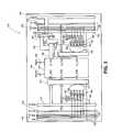
- FIG. 1is a block diagram of an illustrative core tile 102 in an FPGA 100 of the present system.
- FPGA core tile 102comprises an array of logic clusters 104 , static random access memory (SRAM) clusters 106 and static random access memory (SRAM) modules 108 .
- Logic clusters 104 and SRAM clusters 106are connected together by a routing interconnect architecture (not shown) that may comprise multiple levels of routing interconnects.
- FPGA core tile 102is surrounded by input/output ( 110 ) clusters 110 , input/output (I/O) FIFO control blocks 114 and input/output banks 112 .
- I/O clusters 110There are two rows of I/O clusters 110 on the top and bottom edges of FPGA 100 and one column of I/O clusters on the left and right edge of FPGA 100 .
- FIG. 2is a block diagram of an illustrative FPGA including multiple core tiles 102 as shown as an example in FIG. 1 .
- FPGA 120comprises four core tiles 102 , though other numbers of tiles are possible.
- Core tiles 102are surrounded by 110 clusters 110 , input/output FIFO control blocks 114 and I/O banks 112 .
- FIG. 3is a simplified block diagram of a static random access memory (SRAM) block 108 of the present system.
- the present systemcombines dedicated control logic with a two port SRAM to produce a FIFO.
- SRAMstatic random access memory
- FIGS. 1 and 2there are four SRAM blocks 108 along the one side of FPGA tile 102 .
- Each SRAM block 108may be configured to operate as an individual SRAM module or modules may be cascaded together to produce wider or deeper memory combinations.
- dedicated FIFO control logichas been added to each SRAM block.
- SRAM block 108comprises a SRAM component 150 .
- SRAM component 150is a memory component. Memory components are well known to those of ordinary skill in the relevant art and can vary greatly depending on the application.
- Write data bus 152 and write address bus 156are coupled to SRAM component 150 through register 154 .
- Write data enable signal lines 158are each coupled to SRAM component 150 through one input of two-input XOR gates 160 , 162 , 164 , 166 , 168 , AND gate 170 and register 154 .
- the second input of two-input XNOR gates 160 , 162 , 164 , 166 , 168is provided by write enable control lines 172 .
- Register 154receives a clock signal through write clock signal line 159 .
- Read address bus 174is coupled to SRAM component through register 176 .
- Read enable signal lines 178are each coupled to SRAM component 150 through one input of XOR gates 180 , 182 , 184 , 186 , 188 , AND gate 190 and register 176 .
- the second input of register 176receives a clock signal through read clock signal line 192 .
- Input signal busses 194 and 196provide the signals for determining the write word width and read word width respectively.
- Read data bus 198is coupled to the output of SRAM component 150 through register 199 and two-input multiplexer 197 .
- SRAM block 108has multiple bits accessible by two independent ports: a read only port (all circuitry on the right of SRAM block 108 ) and a write only port (all circuitry on the left of SRAM block 108 ). Both ports may be independently configured in multiple words by bits per words combinations. For example, both ports may be configured as 4,096 ⁇ 1, 2,048 ⁇ 2, 1,024 ⁇ 4, 512 ⁇ 9, 256 ⁇ 18 and 128 ⁇ 36. In addition, a plurality of SRAM blocks may be cascaded together by means of busses 152 , 156 , 158 , 174 , 178 , 198 .
- the present examplethere are five enable lines for each port, one for real enable and four for higher order address bits.
- the ten XOR gatesare used to invert or not invert the lines on a block-by-block basis effectively making AND gates 170 and 190 decoders with programmable bubbles on the inputs.
- the write portis synchronous to the write clock and the read port is synchronous to the read clock.
- the above exampleis illustrative only, many other configurations or memory blocks could be used.
- FIG. 4is a simplified schematic diagram illustrating the FIFO logic component 200 of the present invention.
- FIFO logic component 200is coupled between static random access memory (SRAM) clusters 106 and static random access memory (SRAM) block 108 .
- SRAMstatic random access memory
- FIFO logic component 200is coupled between seven static random access memory (SRAM) clusters 106 and static random access memory (SRAM) block 108 .
- Two input AND gate 202has its non-inverting and inverting inputs coupled to random access memory cluster 106 via signal lines 240 and 242 respectively and an output coupled to address comparator 238 , and to subtractor circuit 222 through counter 210 and to address comparator 232 through registers 218 and 220 .
- the output of two-input AND gate 202may also be coupled to RAM module 108 through tri-state buffer 206 .
- the output of counter 210may also be coupled to SRAM block 108 through tri-state buffer 214 .
- Two input AND gate 204has its non-inverting and inverting inputs coupled to SRAM cluster 106 through signal lines 244 and 246 respectively and its output coupled to address comparator 232 through counter 212 .
- Two input AND gate 204also has its output coupled to address comparator 238 through counter 212 , register 224 and register 226 and its output is also coupled to subtracter 222 through counter 212 .
- the output of two-input AND gate 204may also be coupled to SRAM module 108 through tri-state buffer 208 .
- the output of counter 212may also be coupled to SRAM block 108 through tri-state buffer 216 .
- Buffers 206 , 208 , 214 and 216receive their control signals from SRAM clusters 106 programmable configuration bits 248
- subtractor circuit 222has its output coupled to one input of magnitude comparators 234 and 236 .
- Magnitude comparators 234 and 236receive their second input from the programmable configuration bits 228 and 230 respectively.
- the configuration bits in 228 and 230are programmable threshold values need to generate the almost full and almost empty flags respectively.
- Read data bus 250 and write data bus 252are coupled directly to SRAM block 108 .
- controller bits 248are set at 0 disabling the tri-state buffers 206 , 208 214 and 216 .
- all input signalsoriginate from adjacent SRAM clusters 106 .
- a select set of signals from the RAM cluster modulesare set to high impedance and FIFO logic component 200 seizes control of the signal lines.
- FIFO logic component 200seizes control of the write enable signals 158 , the read enable signals 178 and the read and write address lines 174 and 156 respectively as shown in FIG. 3 .
- Counters 210 and 212are binary counters, however, they also generate gray code.
- Gray code or “single distance code”is an ordering of 2 n binary numbers such that only one bit changes between any two consecutive elements.
- the binary valueis sent to subtractor 222 to calculate the difference between the read and write counters for the almost full and almost empty flags.
- the gray codeis sent to address comparators 232 and 238 as well as to tri-state buffers 214 and 216 . In gray code, one and only one bit changes between any two consecutive codes in the sequence.
- the purpose of registers 218 and 220is to synchronize the read counter address in 210 to write clock signal and the purpose of registers 224 and 226 is to synchronize the write counter address to read clock signal for comparison purposes.
- each comparator 232 and 238compares the read and write MSBs. When the two MSBs are equal and the read and write addresses are equal in comparator 238 , this implies a possible empty condition. When the two MSBs are not equal and the read and write addresses are equal in comparator 232 , this implies a possible full condition.
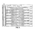
- FIG. 5is a simplified block diagram illustrating the architecture of a RAM cluster 106 of the present system.
- RAM cluster 106may comprise any number of the logic components as indicated below. The examples set forth below are for illustrative purposes only and in no way limit the scope of the present invention.
- Random access memory clusters 106( 0 - 6 ) further comprise two sub-clusters 300 and 302 . Each sub cluster 300 and 302 has two transmitter modules 314 and two receiver modules 312 .
- Right sub cluster 302has a buffer module 316 .
- receiver modules 312 , transmitter modules 314 and buffer module 316are not described in detail herein.
- the implementation of receiver modules 312 and transmitter modules 314 suitable for use according to the present systemis disclosed in U. S. patent application Ser. No. 10/323,613, filed on Dec. 18, 2002, by inventor Arunangshu Kundu, William C. Plants, John McCollum and Venkatesh Narayanan, entitled “A ROUTING ARCHITECHTURE HAVING RECEIVERS AND TRANSMITTERS FOR A FIELD PROGRAMMABLE GATE ARRAY”, having attorney docket number ACT-327, and hereby incorporated herein by reference.
- buffer modules 316suitable for use according to the present system is disclosed in U. S. patent application Ser. No. 10/293,895, filed on Nov. 12, 2002, by inventor William C. Plants, entitled “A FIELD PROGRAMMABLE GATE ARRAY ARCHITECHTURE INCLUDING A BUFFER MODULE AND A METHOD OF DISTRIBUTING BUFFER MODULES IN A FIELD PROGRAMMABLE GATE ARRAY”, having attorney docket number ACT-337, and hereby incorporated herein by reference.
- each SRAM block 108is logically one RAM cluster 106 wide and seven rows long.
- Sub-clusters 300 and 302 of RAM cluster 106 ( 0 )each have one RAM clock interface input (RC) module 304 , six single ended input (RT) modules 306 and two RAM interface output (RO) modules 308 in addition to the two transmitter modules 314 and two receiver modules 312 as set forth above.
- Right sub cluster 302also has a buffer module 316 .
- RC modules 304 in RAM cluster 106select the write and read clock signals from all the HCLK and RCLK networks or from signals in either of two adjacent two routed channels and determine their polarity. RC modules 304 will be discussed in greater detail below.
- Each RT module 306provides a control signal to SRAM module 108 which is either routed from a single channel or tied off to logic 1 or logic 0 .
- RO modules 308transmit read-data or FIFO flags from SRAM module 108 into an individual output track. RT modules 306 and RO modules 308 will be discussed in greater detail below.
- Sub-lusters 300 and 302 of RAM clusters 106each have three two-input RAM channel-up/channel-down non-cascadable signal (RN) modules 310 , three RO modules 308 and six two-input RAM channel-up/channel-down cascadable signal (RI) modules 309 in addition to the two transmitter modules 314 and two receiver modules 312 as set forth above.
- Right sub cluster 302also has a buffer module 316 .
- RN modules 310 and RI modules 309provide an input signal to SRAM module 108 that can be routed from two rows, the one in which it is located and the row immediately above it.
- FIG. 6is a simplified schematic diagram illustrating RT module 306 , RN module 310 , RI module 309 and RO module 308 of a RAM cluster of FIG. 5 .
- RT module 306comprises a buffer 354 that has an input programmably coupled to a horizontal routing track in routing architecture row 352 .
- programmable elementsinclude, but are not limited to, MOS transistors, flash memory cell and antifuses.
- Buffer 354has an output that is coupled to SRAM block 108 .
- RN module 310comprises a two-input AND gate 356 and a buffer 358 .
- One input of two-input AND gate 356is programmably coupled to a horizontal routing track in routing architecture row 350 .
- the second input of two-input AND gate 356is programmably coupled to a horizontal routing track in routing architecture row 352 .
- the output of two-input AND gate 356is coupled to SRAM module 108 through buffer 358 .
- RI module 309comprises a two-input NAND gate 376 having the ability to select a signal from routing architecture row 150 or 152 .
- Two-input NAND gate 376has an output coupled to SRAM block 108 through tri-state buffer 380 and one inverted signal input of a two-input OR gate 378 .
- Two-input OR gatehas a second input coupled to Vcc or ground and its output coupled to SRAM module 108 through tri-state buffer 380 .
- Vccis used to define the positive power supply for the digital circuit as designed.
- the size of a digital circuitmay vary greatly depending on a user's particular circuit requirements. Thus, Vcc may change depending on the size of the circuit elements used.
- RO module 308comprises a buffer 360 having an input coupled to FIFO control block 200 or SRAM block 108 .
- the output of buffer 360requires programming voltage protection and drives an output track which in routing architecture row 352 .
- FIG. 7is a simplified schematic diagram illustrating RC module 304 of a ram cluster of FIG. 5 .
- RC module 304comprises a four input multiplexer 362 having inputs coupled to the clock network bus 370 (not shown).
- Multiplexer 362has an output coupled to a first input of a two-input multiplexer 365 .
- the second input of two-input multiplexer 365is selectively programmably coupled to the routing architecture in rows 372 and 374 through two-input AND gate 364 .
- Two-input multiplexer 365has an output coupled to an input of a two-input XNOR gate that has a second input programmably coupled to Vcc ground in routing architecture row 372 .
- the output of XNOR gate 366is coupled to SRAM block 108 through buffer 368 .
Landscapes
- Physics & Mathematics (AREA)
- Mathematical Physics (AREA)
- Engineering & Computer Science (AREA)
- Computer Hardware Design (AREA)
- Computing Systems (AREA)
- General Engineering & Computer Science (AREA)
- Logic Circuits (AREA)
- Static Random-Access Memory (AREA)
Abstract
Description
Claims (6)
Priority Applications (5)
| Application Number | Priority Date | Filing Date | Title |
|---|---|---|---|
| US10/448,259US6838902B1 (en) | 2003-05-28 | 2003-05-28 | Synchronous first-in/first-out block memory for a field programmable gate array |
| US10/948,010US6980027B2 (en) | 2003-05-28 | 2004-09-22 | Synchronous first-in/first-out block memory for a field programmable gate array |
| US11/297,088US7227380B2 (en) | 2003-05-28 | 2005-12-07 | Synchronous first-in/first-out block memory for a field programmable gate array |
| US11/737,030US7394289B2 (en) | 2003-05-28 | 2007-04-18 | Synchronous first-in/first-out block memory for a field programmable gate array |
| US12/111,648US20080218207A1 (en) | 2003-05-28 | 2008-04-29 | Synchronous first-in/first-out block memory for a field programmable gate array |
Applications Claiming Priority (1)
| Application Number | Priority Date | Filing Date | Title |
|---|---|---|---|
| US10/448,259US6838902B1 (en) | 2003-05-28 | 2003-05-28 | Synchronous first-in/first-out block memory for a field programmable gate array |
Related Child Applications (1)
| Application Number | Title | Priority Date | Filing Date |
|---|---|---|---|
| US10/948,010ContinuationUS6980027B2 (en) | 2003-05-28 | 2004-09-22 | Synchronous first-in/first-out block memory for a field programmable gate array |
Publications (1)
| Publication Number | Publication Date |
|---|---|
| US6838902B1true US6838902B1 (en) | 2005-01-04 |
Family
ID=33538944
Family Applications (5)
| Application Number | Title | Priority Date | Filing Date |
|---|---|---|---|
| US10/448,259Expired - LifetimeUS6838902B1 (en) | 2003-05-28 | 2003-05-28 | Synchronous first-in/first-out block memory for a field programmable gate array |
| US10/948,010Expired - LifetimeUS6980027B2 (en) | 2003-05-28 | 2004-09-22 | Synchronous first-in/first-out block memory for a field programmable gate array |
| US11/297,088Expired - Fee RelatedUS7227380B2 (en) | 2003-05-28 | 2005-12-07 | Synchronous first-in/first-out block memory for a field programmable gate array |
| US11/737,030Expired - LifetimeUS7394289B2 (en) | 2003-05-28 | 2007-04-18 | Synchronous first-in/first-out block memory for a field programmable gate array |
| US12/111,648AbandonedUS20080218207A1 (en) | 2003-05-28 | 2008-04-29 | Synchronous first-in/first-out block memory for a field programmable gate array |
Family Applications After (4)
| Application Number | Title | Priority Date | Filing Date |
|---|---|---|---|
| US10/948,010Expired - LifetimeUS6980027B2 (en) | 2003-05-28 | 2004-09-22 | Synchronous first-in/first-out block memory for a field programmable gate array |
| US11/297,088Expired - Fee RelatedUS7227380B2 (en) | 2003-05-28 | 2005-12-07 | Synchronous first-in/first-out block memory for a field programmable gate array |
| US11/737,030Expired - LifetimeUS7394289B2 (en) | 2003-05-28 | 2007-04-18 | Synchronous first-in/first-out block memory for a field programmable gate array |
| US12/111,648AbandonedUS20080218207A1 (en) | 2003-05-28 | 2008-04-29 | Synchronous first-in/first-out block memory for a field programmable gate array |
Country Status (1)
| Country | Link |
|---|---|
| US (5) | US6838902B1 (en) |
Cited By (78)
| Publication number | Priority date | Publication date | Assignee | Title |
|---|---|---|---|---|
| US7038952B1 (en) | 2004-05-04 | 2006-05-02 | Xilinx, Inc. | Block RAM with embedded FIFO buffer |
| US20060140188A1 (en)* | 2004-12-28 | 2006-06-29 | International Business Machines Corporation | Self-healing link sequence counts within a circular buffer |
| US7106098B1 (en)* | 2004-05-04 | 2006-09-12 | Xilinx, Inc. | Split FIFO configuration of block RAM |
| US7126373B1 (en) | 2004-02-14 | 2006-10-24 | Herman Schmit | Configurable logic circuits with commutative properties |
| US7126381B1 (en) | 2004-02-14 | 2006-10-24 | Herman Schmit | VPA interconnect circuit |
| US20060256636A1 (en)* | 2005-03-31 | 2006-11-16 | Stmicroelectronics Pvt.Ltd. | Configurable length first-in first-out memory |
| US7145361B1 (en) | 2004-06-30 | 2006-12-05 | Andre Rohe | Configurable integrated circuit with different connection schemes |
| US7157933B1 (en) | 2004-02-14 | 2007-01-02 | Herman Schmit | Configurable circuits, IC's, and systems |
| US7161849B1 (en) | 2004-05-04 | 2007-01-09 | Xilinx, Inc. | First-in, first-out buffer system in an integrated circuit |
| US7167025B1 (en)* | 2004-02-14 | 2007-01-23 | Herman Schmit | Non-sequentially configurable IC |
| US7193440B1 (en) | 2004-02-14 | 2007-03-20 | Herman Schmit | Configurable circuits, IC's, and systems |
| US7193432B1 (en) | 2004-02-14 | 2007-03-20 | Herman Schmit | VPA logic circuits |
| US7193438B1 (en) | 2004-06-30 | 2007-03-20 | Andre Rohe | Configurable integrated circuit with offset connection |
| US20070075737A1 (en)* | 2004-02-14 | 2007-04-05 | Herman Schmit | Configurable Circuits, IC's, and Systems |
| US7224182B1 (en) | 2005-03-15 | 2007-05-29 | Brad Hutchings | Hybrid configurable circuit for a configurable IC |
| US7224181B1 (en) | 2004-11-08 | 2007-05-29 | Herman Schmit | Clock distribution in a configurable IC |
| US7227380B2 (en) | 2003-05-28 | 2007-06-05 | Actel Corporation | Synchronous first-in/first-out block memory for a field programmable gate array |
| US7242216B1 (en) | 2004-11-08 | 2007-07-10 | Herman Schmit | Embedding memory between tile arrangement of a configurable IC |
| US20070164784A1 (en)* | 2006-01-19 | 2007-07-19 | Altera Corporation | Modular I/O bank architecture |
| US20070165478A1 (en)* | 2006-01-19 | 2007-07-19 | Jeffrey Tyhach | Modular i/o bank architecture |
| US7254677B1 (en) | 2004-05-04 | 2007-08-07 | Xilinx, Inc. | First-in, first-out memory system with reduced cycle latency |
| US7259587B1 (en) | 2004-11-08 | 2007-08-21 | Tabula, Inc. | Configurable IC's with configurable logic resources that have asymetric inputs and/or outputs |
| US7268586B1 (en) | 2004-11-08 | 2007-09-11 | Tabula, Inc. | Method and apparatus for accessing stored data in a reconfigurable IC |
| US7276933B1 (en) | 2004-11-08 | 2007-10-02 | Tabula, Inc. | Reconfigurable IC that has sections running at different looperness |
| US7284222B1 (en) | 2004-06-30 | 2007-10-16 | Tabula, Inc. | Method and apparatus for identifying connections between configurable nodes in a configurable integrated circuit |
| US7282950B1 (en) | 2004-11-08 | 2007-10-16 | Tabula, Inc. | Configurable IC's with logic resources with offset connections |
| US20070244959A1 (en)* | 2005-03-15 | 2007-10-18 | Steven Teig | Configurable IC's with dual carry chains |
| US20070244961A1 (en)* | 2004-11-08 | 2007-10-18 | Herman Schmit | Configurable IC with configurable routing resources that have asymmetric Input and/or outputs |
| US20070241787A1 (en)* | 2004-06-30 | 2007-10-18 | Herman Schmit | Configurable Circuits, IC's, and Systems |
| US20070241788A1 (en)* | 2004-06-30 | 2007-10-18 | Herman Schmit | VPA Logic Circuits |
| US20070241781A1 (en)* | 2005-03-15 | 2007-10-18 | Brad Hutchings | Variable width management for a memory of a configurable IC |
| US20070241784A1 (en)* | 2005-03-15 | 2007-10-18 | Brad Hutchings | Configurable ic with interconnect circuits that have select lines driven by user signals |
| US20070241776A1 (en)* | 2004-06-30 | 2007-10-18 | Herman Schmit | Configurable Logic Circuits with Commutative Properties |
| US20070241773A1 (en)* | 2005-03-15 | 2007-10-18 | Brad Hutchings | Hybrid logic/interconnect circuit in a configurable ic |
| US20070257700A1 (en)* | 2005-03-15 | 2007-11-08 | Andrew Caldwell | Method and apparatus for decomposing functions in a configurable IC |
| US7295037B2 (en) | 2004-11-08 | 2007-11-13 | Tabula, Inc. | Configurable IC with routing circuits with offset connections |
| US7301368B2 (en) | 2005-03-15 | 2007-11-27 | Tabula, Inc. | Embedding memory within tile arrangement of a configurable IC |
| US7312630B2 (en) | 2004-06-30 | 2007-12-25 | Tabula, Inc. | Configurable integrated circuit with built-in turns |
| US7317331B2 (en) | 2004-11-08 | 2008-01-08 | Tabula, Inc. | Reconfigurable IC that has sections running at different reconfiguration rates |
| US7330050B2 (en) | 2004-11-08 | 2008-02-12 | Tabula, Inc. | Storage elements for a configurable IC and method and apparatus for accessing data stored in the storage elements |
| US7342415B2 (en) | 2004-11-08 | 2008-03-11 | Tabula, Inc. | Configurable IC with interconnect circuits that also perform storage operations |
| US7346739B1 (en) | 2004-11-19 | 2008-03-18 | Xilinx, Inc. | First-in-first-out memory system and method for providing same |
| US7359276B1 (en) | 2005-09-27 | 2008-04-15 | Xilinx, Inc. | Multi-port system for communication between processing elements |
| US7425841B2 (en) | 2004-02-14 | 2008-09-16 | Tabula Inc. | Configurable circuits, IC's, and systems |
| US20080231315A1 (en)* | 2007-03-20 | 2008-09-25 | Steven Teig | Configurable IC Having A Routing Fabric With Storage Elements |
| US20080231319A1 (en)* | 2003-05-30 | 2008-09-25 | Actel Corporation | Dedicated input/output first in/first out module for a field programmable gate array |
| US7461362B1 (en) | 2005-12-01 | 2008-12-02 | Tabula, Inc. | Replacing circuit design elements with their equivalents |
| US7489162B1 (en) | 2005-12-01 | 2009-02-10 | Tabula, Inc. | Users registers in a reconfigurable IC |
| US7504858B1 (en) | 2006-03-08 | 2009-03-17 | Tabula, Inc. | Configurable integrated circuit with parallel non-neighboring offset connections |
| US7518400B1 (en) | 2006-03-08 | 2009-04-14 | Tabula, Inc. | Barrel shifter implemented on a configurable integrated circuit |
| US7529992B1 (en) | 2006-03-27 | 2009-05-05 | Tabula, Inc. | Configurable integrated circuit with error correcting circuitry |
| US7535252B1 (en) | 2007-03-22 | 2009-05-19 | Tabula, Inc. | Configurable ICs that conditionally transition through configuration data sets |
| US20090146689A1 (en)* | 2007-09-06 | 2009-06-11 | Trevis Chandler | Configuration Context Switcher with a Clocked Storage Element |
| US7587698B1 (en) | 2004-12-01 | 2009-09-08 | Tabula Inc. | Operational time extension |
| US7587697B1 (en) | 2006-12-12 | 2009-09-08 | Tabula, Inc. | System and method of mapping memory blocks in a configurable integrated circuit |
| US7609085B1 (en) | 2006-03-08 | 2009-10-27 | Tabula, Inc. | Configurable integrated circuit with a 4-to-1 multiplexer |
| US20090327987A1 (en)* | 2008-06-26 | 2009-12-31 | Steven Teig | Timing operations in an IC with configurable circuits |
| US7669097B1 (en) | 2006-03-27 | 2010-02-23 | Tabula, Inc. | Configurable IC with error detection and correction circuitry |
| US7676661B1 (en) | 2004-10-05 | 2010-03-09 | Xilinx, Inc. | Method and system for function acceleration using custom instructions |
| US7679401B1 (en) | 2005-12-01 | 2010-03-16 | Tabula, Inc. | User registers implemented with routing circuits in a configurable IC |
| US7694083B1 (en) | 2006-03-08 | 2010-04-06 | Tabula, Inc. | System and method for providing a virtual memory architecture narrower and deeper than a physical memory architecture |
| US20100097099A1 (en)* | 2004-11-01 | 2010-04-22 | Deboleena Minz | FPGA Having a Direct Routing Structure |
| US7743085B2 (en) | 2004-11-08 | 2010-06-22 | Tabula, Inc. | Configurable IC with large carry chains |
| US7765249B1 (en) | 2005-11-07 | 2010-07-27 | Tabula, Inc. | Use of hybrid interconnect/logic circuits for multiplication |
| US7797497B1 (en) | 2006-03-08 | 2010-09-14 | Tabula, Inc. | System and method for providing more logical memory ports than physical memory ports |
| US7804730B2 (en) | 2005-03-15 | 2010-09-28 | Tabula, Inc. | Method and apparatus for accessing contents of memory cells |
| US7818361B1 (en) | 2005-11-07 | 2010-10-19 | Tabula, Inc. | Method and apparatus for performing two's complement multiplication |
| US7917559B2 (en) | 2004-11-08 | 2011-03-29 | Tabula, Inc. | Configurable IC's with configurable logic circuits that perform adder and/or subtractor operations |
| US7930666B1 (en) | 2006-12-12 | 2011-04-19 | Tabula, Inc. | System and method of providing a memory hierarchy |
| US7971172B1 (en) | 2005-11-07 | 2011-06-28 | Tabula, Inc. | IC that efficiently replicates a function to save logic and routing resources |
| US8463836B1 (en) | 2005-11-07 | 2013-06-11 | Tabula, Inc. | Performing mathematical and logical operations in multiple sub-cycles |
| US8611173B1 (en) | 2011-12-02 | 2013-12-17 | Altera Corporation | Buffer circuitry with multiport memory cells |
| US8760193B2 (en) | 2011-07-01 | 2014-06-24 | Tabula, Inc. | Configurable storage elements |
| US8863067B1 (en) | 2008-02-06 | 2014-10-14 | Tabula, Inc. | Sequential delay analysis by placement engines |
| US8912820B2 (en) | 2010-04-02 | 2014-12-16 | Tabula, Inc. | System and method for reducing reconfiguration power |
| US9148151B2 (en) | 2011-07-13 | 2015-09-29 | Altera Corporation | Configurable storage elements |
| US9203397B1 (en) | 2011-12-16 | 2015-12-01 | Altera Corporation | Delaying start of user design execution |
| US9583190B2 (en) | 2011-11-11 | 2017-02-28 | Altera Corporation | Content addressable memory in integrated circuit |
Families Citing this family (5)
| Publication number | Priority date | Publication date | Assignee | Title |
|---|---|---|---|---|
| US6150837A (en)* | 1997-02-28 | 2000-11-21 | Actel Corporation | Enhanced field programmable gate array |
| US7495970B1 (en)* | 2006-06-02 | 2009-02-24 | Lattice Semiconductor Corporation | Flexible memory architectures for programmable logic devices |
| US7539789B1 (en) | 2006-08-14 | 2009-05-26 | Xilinx, Inc. | Circuits providing greater depth and/or asymmetric access ports for first-in first-out memory circuits (FIFOs) |
| US7535789B1 (en)* | 2006-09-27 | 2009-05-19 | Xilinx, Inc. | Circuits and methods of concatenating FIFOs |
| US8446170B2 (en) | 2011-05-05 | 2013-05-21 | Actel Corporation | FPGA RAM blocks optimized for use as register files |
Citations (117)
| Publication number | Priority date | Publication date | Assignee | Title |
|---|---|---|---|---|
| US4255748A (en) | 1979-02-12 | 1981-03-10 | Automation Systems, Inc. | Bus fault detector |
| US4625313A (en) | 1984-07-06 | 1986-11-25 | Tektronix, Inc. | Method and apparatus for testing electronic equipment |
| US4638187A (en) | 1985-10-01 | 1987-01-20 | Vtc Incorporated | CMOS output buffer providing high drive current with minimum output signal distortion |
| US4638243A (en) | 1985-06-05 | 1987-01-20 | Monolithic Memories, Inc. | Short detector for fusible link array using single reference fuse |
| US4684830A (en) | 1985-03-22 | 1987-08-04 | Monolithic Memories, Inc. | Output circuit for a programmable logic array |
| US4700130A (en) | 1980-03-12 | 1987-10-13 | U.S. Philips Corporation | Current-measuring arrangement with overload protection |
| US4706216A (en) | 1985-02-27 | 1987-11-10 | Xilinx, Inc. | Configurable logic element |
| US4713557A (en) | 1984-09-26 | 1987-12-15 | Xilinx, Inc. | Bidirectional buffer amplifier |
| US4718042A (en) | 1985-12-23 | 1988-01-05 | Ncr Corporation | Non-destructive method and circuit to determine the programmability of a one time programmable device |
| US4717912A (en) | 1982-10-07 | 1988-01-05 | Advanced Micro Devices, Inc. | Apparatus for producing any one of a plurality of signals at a single output |
| US4742252A (en) | 1985-03-29 | 1988-05-03 | Advanced Micro Devices, Inc. | Multiple array customizable logic device |
| US4772812A (en) | 1981-07-27 | 1988-09-20 | Data General Corporation | Tri-state output buffer circuit including a capacitor and dynamic depletion mode switching device |
| US4800176A (en) | 1987-05-29 | 1989-01-24 | Kabushiki Kaisha Toshiba | Method for forming contact portion in semiconductor integrated circuit devices |
| US4857774A (en) | 1986-09-19 | 1989-08-15 | Actel Corporation | Testing apparatus and diagnostic method for use with programmable interconnect architecture |
| US4870302A (en) | 1984-03-12 | 1989-09-26 | Xilinx, Inc. | Configurable electrical circuit having configurable logic elements and configurable interconnects |
| US4870300A (en) | 1986-08-06 | 1989-09-26 | Mitsubishi Denki Kabushiki Kaisha | Standard cell system large scale integrated circuit with heavy load lines passing through the cells |
| US4873459A (en) | 1986-09-19 | 1989-10-10 | Actel Corporation | Programmable interconnect architecture |
| US4928023A (en) | 1987-08-27 | 1990-05-22 | Texas Instruments Incorporated | Improved output buffer having reduced noise characteristics |
| US4930097A (en) | 1988-12-30 | 1990-05-29 | Intel Corporation | Architecture for an improved performance of a programmable logic device |
| US4935645A (en) | 1988-03-02 | 1990-06-19 | Dallas Semiconductor Corporation | Fusing and detection circuit |
| US4959561A (en) | 1989-01-04 | 1990-09-25 | Motorola, Inc. | MOS output buffer with reduced supply line disturbance |
| US4978905A (en) | 1989-10-31 | 1990-12-18 | Cypress Semiconductor Corp. | Noise reduction output buffer |
| EP0415542A2 (en) | 1989-08-15 | 1991-03-06 | Advanced Micro Devices, Inc. | Programmable gate array with improved interconnect structure, input/output structure and configurable logic block |
| US5008855A (en) | 1989-07-18 | 1991-04-16 | Actel Corporation | Method of programming anti-fuse element |
| US5046035A (en) | 1987-08-26 | 1991-09-03 | Ict International Cmos Tech., Inc. | High-performance user programmable logic device (PLD) |
| US5083083A (en) | 1986-09-19 | 1992-01-21 | Actel Corporation | Testability architecture and techniques for programmable interconnect architecture |
| US5121394A (en) | 1989-12-20 | 1992-06-09 | Bull Hn Information Systems Inc. | Method of organizing programmable logic array devices for board testability |
| US5122685A (en) | 1991-03-06 | 1992-06-16 | Quicklogic Corporation | Programmable application specific integrated circuit and logic cell therefor |
| US5126282A (en) | 1990-05-16 | 1992-06-30 | Actel Corporation | Methods of reducing anti-fuse resistance during programming |
| US5132571A (en) | 1990-08-01 | 1992-07-21 | Actel Corporation | Programmable interconnect architecture having interconnects disposed above function modules |
| US5144166A (en) | 1990-11-02 | 1992-09-01 | Concurrent Logic, Inc. | Programmable logic cell and array |
| US5187392A (en) | 1991-07-31 | 1993-02-16 | Intel Corporation | Programmable logic device with limited signal swing |
| US5198705A (en) | 1990-05-11 | 1993-03-30 | Actel Corporation | Logic module with configurable combinational and sequential blocks |
| US5208491A (en) | 1992-01-07 | 1993-05-04 | Washington Research Foundation | Field programmable gate array |
| US5220213A (en) | 1991-03-06 | 1993-06-15 | Quicklogic Corporation | Programmable application specific integrated circuit and logic cell therefor |
| US5220215A (en) | 1992-05-15 | 1993-06-15 | Micron Technology, Inc. | Field programmable logic array with two or planes |
| US5221865A (en) | 1991-06-21 | 1993-06-22 | Crosspoint Solutions, Inc. | Programmable input/output buffer circuit with test capability |
| US5222066A (en) | 1990-12-26 | 1993-06-22 | Motorola, Inc. | Modular self-test for embedded SRAMS |
| US5258319A (en) | 1988-02-19 | 1993-11-02 | Mitsubishi Denki Kabushiki Kaisha | Method of manufacturing a MOS type field effect transistor using an oblique ion implantation step |
| US5272388A (en) | 1992-06-09 | 1993-12-21 | Actel Corporation | High-yield methods for programming antifuses |
| US5293133A (en) | 1992-08-27 | 1994-03-08 | Quicklogic Corporation | Method of determining an electrical characteristic of an antifuse and apparatus therefor |
| US5300832A (en) | 1992-11-10 | 1994-04-05 | Sun Microsystems, Inc. | Voltage interfacing buffer with isolation transistors used for overvoltage protection |
| US5300830A (en) | 1992-05-15 | 1994-04-05 | Micron Semiconductor, Inc. | Programmable logic device macrocell with an exclusive feedback and exclusive external input lines for registered and combinatorial modes using a dedicated product term for control |
| US5317698A (en) | 1992-08-18 | 1994-05-31 | Actel Corporation | FPGA architecture including direct logic function circuit to I/O interconnections |
| US5365485A (en) | 1993-11-22 | 1994-11-15 | Texas Instruments Incorporated | Fifo with fast retransmit mode |
| US5367207A (en) | 1990-12-04 | 1994-11-22 | Xilinx, Inc. | Structure and method for programming antifuses in an integrated circuit array |
| US5375089A (en) | 1993-10-05 | 1994-12-20 | Advanced Micro Devices, Inc. | Plural port memory system utilizing a memory having a read port and a write port |
| US5394034A (en) | 1992-07-27 | 1995-02-28 | Siemens Aktiengesellschaft | Programmable logic array having programmable output driver drive capacity |
| US5394033A (en) | 1993-09-01 | 1995-02-28 | Lattice Semiconductor Corporation | Structure and method for implementing hierarchical routing pools in a programmable logic circuit |
| US5396128A (en) | 1993-09-13 | 1995-03-07 | Motorola, Inc. | Output circuit for interfacing integrated circuits having different power supply potentials |
| US5397939A (en) | 1991-07-31 | 1995-03-14 | Quicklogic Corporation | Programming of antifuses |
| US5400262A (en) | 1989-09-20 | 1995-03-21 | Aptix Corporation | Universal interconnect matrix array |
| US5399920A (en) | 1993-11-09 | 1995-03-21 | Texas Instruments Incorporated | CMOS driver which uses a higher voltage to compensate for threshold loss of the pull-up NFET |
| US5430335A (en) | 1991-05-15 | 1995-07-04 | Oki Electric Industry Co., Ltd. | Simplified low-noise output buffer circuit |
| US5430687A (en) | 1994-04-01 | 1995-07-04 | Xilinx, Inc. | Programmable logic device including a parallel input device for loading memory cells |
| US5469396A (en) | 1994-06-07 | 1995-11-21 | Actel Corporation | Apparatus and method determining the resistance of antifuses in an array |
| US5469003A (en) | 1992-11-05 | 1995-11-21 | Xilinx, Inc. | Hierarchically connectable configurable cellular array |
| US5473268A (en) | 1992-05-18 | 1995-12-05 | Ecole Polytechnique Federale De Lausanne | Intermediary circuit between a low voltage logic circuit and a high voltage output stage in standard CMOS technology |
| US5485103A (en) | 1991-09-03 | 1996-01-16 | Altera Corporation | Programmable logic array with local and global conductors |
| US5486775A (en) | 1993-11-22 | 1996-01-23 | Altera Corporation | Multiplexer structures for use in making controllable interconnections in integrated circuits. |
| US5537057A (en) | 1995-02-14 | 1996-07-16 | Altera Corporation | Programmable logic array device with grouped logic regions and three types of conductors |
| US5546019A (en) | 1995-08-24 | 1996-08-13 | Taiwan Semiconductor Manufacture Company | CMOS I/O circuit with 3.3 volt output and tolerance of 5 volt input |
| US5559464A (en) | 1993-07-06 | 1996-09-24 | Seiko Epson Corporation | Signal voltage level conversion circuit and output buffer circuit |
| US5602780A (en)* | 1993-10-20 | 1997-02-11 | Texas Instruments Incorporated | Serial to parallel and parallel to serial architecture for a RAM based FIFO memory |
| US5666322A (en) | 1995-09-21 | 1997-09-09 | Nec Electronics, Inc. | Phase-locked loop timing controller in an integrated circuit memory |
| US5670905A (en) | 1994-07-20 | 1997-09-23 | Micron Technology, Inc. | Low-to-high voltage CMOS driver circuit for driving capacitive loads |
| US5744979A (en) | 1992-07-23 | 1998-04-28 | Xilinx, Inc. | FPGA having logic cells configured by SRAM memory cells and interconnect configured by antifuses |
| US5744980A (en)* | 1996-02-16 | 1998-04-28 | Actel Corporation | Flexible, high-performance static RAM architecture for field-programmable gate arrays |
| US5801547A (en) | 1996-03-01 | 1998-09-01 | Xilinx, Inc. | Embedded memory for field programmable gate array |
| US5809281A (en) | 1993-03-30 | 1998-09-15 | Altera Corporation | Field programmable gate array with high speed SRAM based configurable function block configurable as high performance logic or block of SRAM |
| US5815004A (en) | 1995-10-16 | 1998-09-29 | Xilinx, Inc. | Multi-buffered configurable logic block output lines in a field programmable gate array |
| US5815003A (en) | 1994-11-04 | 1998-09-29 | Altera Corporation | Programmable logic integrated circuits with partitioned logic element using shared lab-wide signals |
| US5821776A (en) | 1997-01-31 | 1998-10-13 | Actel Corporation | Field programmable gate array with mask programmed analog function circuits |
| US5825662A (en) | 1995-08-18 | 1998-10-20 | Xilinx, Inc. | Computer-implemented method of optimizing a time multiplexed programmable logic device |
| US5825202A (en) | 1996-09-26 | 1998-10-20 | Xilinx, Inc. | Integrated circuit with field programmable and application specific logic areas |
| US5825200A (en) | 1996-06-21 | 1998-10-20 | Quicklogic Corporation | Programming architecture for a programmable integrated circuit employing antifuses |
| US5828230A (en) | 1997-01-09 | 1998-10-27 | Xilinx, Inc. | FPGA two turn routing structure with lane changing and minimum diffusion area |
| US5828538A (en) | 1996-06-21 | 1998-10-27 | Quicklogic Corporation | Power-up circuit for field programmable gate arrays |
| US5835998A (en) | 1996-04-04 | 1998-11-10 | Altera Corporation | Logic cell for programmable logic devices |
| US5832892A (en) | 1996-10-11 | 1998-11-10 | Yaoita; Yasuhito | Spark ignition internal combustion engine |
| US5835165A (en) | 1995-06-07 | 1998-11-10 | Lsi Logic Corporation | Reduction of false locking code words in concatenated decoders |
| US5838167A (en) | 1995-05-26 | 1998-11-17 | Xilinx, Inc. | Method and structure for loading data into several IC devices |
| US5838954A (en) | 1995-08-18 | 1998-11-17 | Xilinx, Inc. | Computer-implemented method of optimizing a time multiplexed programmable logic device |
| US5838584A (en) | 1995-01-27 | 1998-11-17 | Altera Corporation | Optimizing chain placement in a programmable logic device |
| US5848005A (en) | 1991-09-03 | 1998-12-08 | Altera Corporation | Programmable logic array integrated circuits |
| US5847441A (en) | 1996-05-10 | 1998-12-08 | Micron Technology, Inc. | Semiconductor junction antifuse circuit |
| US5848006A (en) | 1995-12-06 | 1998-12-08 | Nec Corporation | Redundant semiconductor memory device using a single now address decoder for driving both sub-wordlines and redundant sub-wordlines |
| US5847577A (en) | 1995-02-24 | 1998-12-08 | Xilinx, Inc. | DRAM memory cell for programmable logic devices |
| US5850152A (en) | 1995-05-17 | 1998-12-15 | Altera Corporation | Programmable logic array integrated circuit devices |
| US5850564A (en) | 1995-05-03 | 1998-12-15 | Btr, Inc, | Scalable multiple level tab oriented interconnect architecture |
| US5852608A (en) | 1996-06-06 | 1998-12-22 | Sun Microsystems, Inc. | Structure and method for bi-directional data transfer between asynchronous clock domains |
| US5854763A (en) | 1997-01-31 | 1998-12-29 | Mosaid Technologies Inc. | Integrated circuit with non-binary decoding and data access |
| EP0889593A1 (en) | 1994-05-19 | 1999-01-07 | Actel Corporation | Programmable logic module for field programmable gate array device |
| US5859544A (en) | 1996-09-05 | 1999-01-12 | Altera Corporation | Dynamic configurable elements for programmable logic devices |
| US5870586A (en) | 1996-01-31 | 1999-02-09 | Xilinx, Inc. | Configuration emulation of a programmable logic device |
| US5869981A (en) | 1985-03-29 | 1999-02-09 | Advanced Micro Devices, Inc. | High density programmable logic device |
| US5880492A (en) | 1995-10-16 | 1999-03-09 | Xilinx, Inc. | Dedicated local line interconnect layout |
| US5880597A (en) | 1996-09-18 | 1999-03-09 | Altera Corporation | Interleaved interconnect for programmable logic array devices |
| US5880512A (en) | 1991-04-26 | 1999-03-09 | Quicklogic Corporation | Programmable interconnect structures and programmable integrated circuits |
| US5880598A (en) | 1997-01-10 | 1999-03-09 | Xilinx, Inc. | Tile-based modular routing resources for high density programmable logic device |
| US5883526A (en) | 1997-04-17 | 1999-03-16 | Altera Corporation | Hierarchical interconnect for programmable logic devices |
| US5883850A (en) | 1991-09-03 | 1999-03-16 | Altera Corporation | Programmable logic array integrated circuits |
| US5949719A (en) | 1995-12-20 | 1999-09-07 | International Business Machines Corporation | Field programmable memory array |
| US5952847A (en) | 1996-06-25 | 1999-09-14 | Actel Corporation | Multiple logic family compatible output driver |
| US5994934A (en) | 1998-01-13 | 1999-11-30 | Mitsubishi Denki Kabushiki Kaisha | Delay locked loop circuit |
| US6011744A (en) | 1997-07-16 | 2000-01-04 | Altera Corporation | Programmable logic device with multi-port memory |
| US6034677A (en) | 1997-10-17 | 2000-03-07 | Sony Corporation | Method and apparatus for displaying an electronic program guide |
| US6038627A (en) | 1998-03-16 | 2000-03-14 | Actel Corporation | SRAM bus architecture and interconnect to an FPGA |
| US6049487A (en) | 1998-03-16 | 2000-04-11 | Actel Corporation | Embedded static random access memory for field programmable gate array |
| US6111448A (en) | 1997-09-10 | 2000-08-29 | Nec Corporation | Clock signal distribution circuit |
| US6181174B1 (en) | 1998-09-24 | 2001-01-30 | Fujitsu Limited | Semiconductor integrated circuit device |
| US6191996B1 (en)* | 1998-10-01 | 2001-02-20 | Nec Corporation | Semiconductor memory device and data transmission method |
| US6289068B1 (en) | 1998-06-22 | 2001-09-11 | Xilinx, Inc. | Delay lock loop with clock phase shifter |
| US6292016B1 (en) | 1995-10-16 | 2001-09-18 | Altera Corporation | Programmable logic with on-chip DLL or PLL to distribute clock |
| EP1137188A2 (en) | 2000-03-24 | 2001-09-26 | STMicroelectronics, Inc. | Digital phase lock loop |
| US6329839B1 (en) | 1996-09-04 | 2001-12-11 | Advantage Logic, Inc. | Method and apparatus for universal program controlled bus architecture |
| US6437650B1 (en) | 1999-01-08 | 2002-08-20 | Altera Corporation | Phase-locked loop or delay-locked loop circuitry for programmable logic devices |
Family Cites Families (39)
| Publication number | Priority date | Publication date | Assignee | Title |
|---|---|---|---|---|
| US5208530A (en) | 1986-09-19 | 1993-05-04 | Actel Corporation | Testability architecture and techniques for programmable interconnect architecture |
| US5365165A (en)* | 1986-09-19 | 1994-11-15 | Actel Corporation | Testability architecture and techniques for programmable interconnect architecture |
| US5309091A (en) | 1986-09-19 | 1994-05-03 | Actel Corporation | Testability architecture and techniques for programmable interconnect architecture |
| US5341092A (en)* | 1986-09-19 | 1994-08-23 | Actel Corporation | Testability architecture and techniques for programmable interconnect architecture |
| US5223792A (en) | 1986-09-19 | 1993-06-29 | Actel Corporation | Testability architecture and techniques for programmable interconnect architecture |
| IL96808A (en)* | 1990-04-18 | 1996-03-31 | Rambus Inc | Integrated circuit i/o using a high performance bus interface |
| US5191241A (en) | 1990-08-01 | 1993-03-02 | Actel Corporation | Programmable interconnect architecture |
| US5286992A (en)* | 1990-09-28 | 1994-02-15 | Actel Corporation | Low voltage device in a high voltage substrate |
| US5361165A (en)* | 1992-01-03 | 1994-11-01 | General Motors Corporation | Reflective cluster display with stowable viewing screen |
| US5286922A (en)* | 1992-07-14 | 1994-02-15 | Curtiss Thomas E | Fluorescent coated wire |
| US5304871A (en) | 1992-07-24 | 1994-04-19 | Actel Corporation | Programmable interconnect architecture employing leaky programmable elements |
| US5294846A (en) | 1992-08-17 | 1994-03-15 | Paivinen John O | Method and apparatus for programming anti-fuse devices |
| EP0587406B1 (en)* | 1992-09-09 | 1997-11-12 | Matsushita Electric Industrial Co., Ltd. | Combination push switch device |
| US5455525A (en)* | 1993-12-06 | 1995-10-03 | Intelligent Logic Systems, Inc. | Hierarchically-structured programmable logic array and system for interconnecting logic elements in the logic array |
| US5495181A (en)* | 1994-12-01 | 1996-02-27 | Quicklogic Corporation | Integrated circuit facilitating simultaneous programming of multiple antifuses |
| US6049223A (en)* | 1995-03-22 | 2000-04-11 | Altera Corporation | Programmable logic array integrated circuit with general-purpose memory configurable as a random access or FIFO memory |
| US5757207A (en)* | 1995-03-22 | 1998-05-26 | Altera Corporation | Programmable logic array integrated circuit incorporating a first-in first-out memory |
| US5594363A (en)* | 1995-04-07 | 1997-01-14 | Zycad Corporation | Logic cell and routing architecture in a field programmable gate array |
| US5600264A (en)* | 1995-10-16 | 1997-02-04 | Xilinx, Inc. | Programmable single buffered six pass transistor configuration |
| US5804986A (en)* | 1995-12-29 | 1998-09-08 | Cypress Semiconductor Corp. | Memory in a programmable logic device |
| US5977791A (en)* | 1996-04-15 | 1999-11-02 | Altera Corporation | Embedded memory block with FIFO mode for programmable logic device |
| US5742181A (en)* | 1996-06-04 | 1998-04-21 | Hewlett-Packard Co. | FPGA with hierarchical interconnect structure and hyperlinks |
| US5870327A (en)* | 1996-07-19 | 1999-02-09 | Xilinx, Inc. | Mixed mode RAM/ROM cell using antifuses |
| US6100715A (en)* | 1998-12-15 | 2000-08-08 | Vantis Corporation | Methods for configuring FPGA's having variable grain blocks and logic for providing time-shared access to interconnect resources |
| US6260182B1 (en)* | 1998-03-27 | 2001-07-10 | Xilinx, Inc. | Method for specifying routing in a logic module by direct module communication |
| US6216258B1 (en)* | 1998-03-27 | 2001-04-10 | Xilinx, Inc. | FPGA modules parameterized by expressions |
| US6292925B1 (en)* | 1998-03-27 | 2001-09-18 | Xilinx, Inc. | Context-sensitive self implementing modules |
| US6157213A (en) | 1998-10-19 | 2000-12-05 | Xilinx, Inc. | Layout architecture and method for fabricating PLDs including multiple discrete devices formed on a single chip |
| US6242943B1 (en)* | 1998-12-31 | 2001-06-05 | Khaled Ahmad El-Ayat | Programmable multi-standard I/O architecture for FPGAS |
| US6353334B1 (en)* | 2000-01-27 | 2002-03-05 | Xilinx, Inc. | Circuit for converting a logic signal on an output node to a pair of low-voltage differential signals |
| US6535043B2 (en) | 2000-05-26 | 2003-03-18 | Lattice Semiconductor Corp | Clock signal selection system, method of generating a clock signal and programmable clock manager including same |
| US6418059B1 (en)* | 2000-06-26 | 2002-07-09 | Intel Corporation | Method and apparatus for non-volatile memory bit sequence program controller |
| US6501295B1 (en) | 2001-06-01 | 2002-12-31 | Sun Microsystems, Inc. | Overdriven pass transistors |
| US6891394B1 (en)* | 2002-06-04 | 2005-05-10 | Actel Corporation | Field-programmable gate array low voltage differential signaling driver utilizing two complimentary output buffers |
| US6734702B1 (en)* | 2002-11-12 | 2004-05-11 | Texas Instruments Incorporated | Impedance calibration circuit |
| US6727726B1 (en)* | 2002-11-12 | 2004-04-27 | Actel Corporation | Field programmable gate array architecture including a buffer module and a method of distributing buffer modules in a field programmable gate array |
| US6838902B1 (en)* | 2003-05-28 | 2005-01-04 | Actel Corporation | Synchronous first-in/first-out block memory for a field programmable gate array |
| US7199609B1 (en)* | 2003-05-30 | 2007-04-03 | Actel Corporation | Dedicated input/output first in/first out module for a field programmable gate array |
| US6867615B1 (en)* | 2003-05-30 | 2005-03-15 | Actel Corporation | Dedicated input/output first in/first out module for a field programmable gate array |
- 2003
- 2003-05-28USUS10/448,259patent/US6838902B1/ennot_activeExpired - Lifetime
- 2004
- 2004-09-22USUS10/948,010patent/US6980027B2/ennot_activeExpired - Lifetime
- 2005
- 2005-12-07USUS11/297,088patent/US7227380B2/ennot_activeExpired - Fee Related
- 2007
- 2007-04-18USUS11/737,030patent/US7394289B2/ennot_activeExpired - Lifetime
- 2008
- 2008-04-29USUS12/111,648patent/US20080218207A1/ennot_activeAbandoned
Patent Citations (130)
| Publication number | Priority date | Publication date | Assignee | Title |
|---|---|---|---|---|
| US4255748A (en) | 1979-02-12 | 1981-03-10 | Automation Systems, Inc. | Bus fault detector |
| US4700130A (en) | 1980-03-12 | 1987-10-13 | U.S. Philips Corporation | Current-measuring arrangement with overload protection |
| US4772812A (en) | 1981-07-27 | 1988-09-20 | Data General Corporation | Tri-state output buffer circuit including a capacitor and dynamic depletion mode switching device |
| US4717912A (en) | 1982-10-07 | 1988-01-05 | Advanced Micro Devices, Inc. | Apparatus for producing any one of a plurality of signals at a single output |
| US4870302A (en) | 1984-03-12 | 1989-09-26 | Xilinx, Inc. | Configurable electrical circuit having configurable logic elements and configurable interconnects |
| US4625313A (en) | 1984-07-06 | 1986-11-25 | Tektronix, Inc. | Method and apparatus for testing electronic equipment |
| US4713557A (en) | 1984-09-26 | 1987-12-15 | Xilinx, Inc. | Bidirectional buffer amplifier |
| US4706216A (en) | 1985-02-27 | 1987-11-10 | Xilinx, Inc. | Configurable logic element |
| US4684830A (en) | 1985-03-22 | 1987-08-04 | Monolithic Memories, Inc. | Output circuit for a programmable logic array |
| US4742252A (en) | 1985-03-29 | 1988-05-03 | Advanced Micro Devices, Inc. | Multiple array customizable logic device |
| US5869981A (en) | 1985-03-29 | 1999-02-09 | Advanced Micro Devices, Inc. | High density programmable logic device |
| US4638243A (en) | 1985-06-05 | 1987-01-20 | Monolithic Memories, Inc. | Short detector for fusible link array using single reference fuse |
| US4638187A (en) | 1985-10-01 | 1987-01-20 | Vtc Incorporated | CMOS output buffer providing high drive current with minimum output signal distortion |
| US4638187B1 (en) | 1985-10-01 | 1993-03-02 | Cypress Semiconductor Minnesot | |
| US4718042A (en) | 1985-12-23 | 1988-01-05 | Ncr Corporation | Non-destructive method and circuit to determine the programmability of a one time programmable device |
| US4870300A (en) | 1986-08-06 | 1989-09-26 | Mitsubishi Denki Kabushiki Kaisha | Standard cell system large scale integrated circuit with heavy load lines passing through the cells |
| US4873459B1 (en) | 1986-09-19 | 1995-01-10 | Actel Corp | Programmable interconnect architecture |
| US5083083A (en) | 1986-09-19 | 1992-01-21 | Actel Corporation | Testability architecture and techniques for programmable interconnect architecture |
| US4857774A (en) | 1986-09-19 | 1989-08-15 | Actel Corporation | Testing apparatus and diagnostic method for use with programmable interconnect architecture |
| US4873459A (en) | 1986-09-19 | 1989-10-10 | Actel Corporation | Programmable interconnect architecture |
| US4800176A (en) | 1987-05-29 | 1989-01-24 | Kabushiki Kaisha Toshiba | Method for forming contact portion in semiconductor integrated circuit devices |
| US5046035A (en) | 1987-08-26 | 1991-09-03 | Ict International Cmos Tech., Inc. | High-performance user programmable logic device (PLD) |
| US4928023A (en) | 1987-08-27 | 1990-05-22 | Texas Instruments Incorporated | Improved output buffer having reduced noise characteristics |
| US5258319A (en) | 1988-02-19 | 1993-11-02 | Mitsubishi Denki Kabushiki Kaisha | Method of manufacturing a MOS type field effect transistor using an oblique ion implantation step |
| US4935645A (en) | 1988-03-02 | 1990-06-19 | Dallas Semiconductor Corporation | Fusing and detection circuit |
| US4930097A (en) | 1988-12-30 | 1990-05-29 | Intel Corporation | Architecture for an improved performance of a programmable logic device |
| US4959561A (en) | 1989-01-04 | 1990-09-25 | Motorola, Inc. | MOS output buffer with reduced supply line disturbance |
| US5008855A (en) | 1989-07-18 | 1991-04-16 | Actel Corporation | Method of programming anti-fuse element |
| EP0415542A3 (en) | 1989-08-15 | 1991-10-02 | Advanced Micro Devices, Inc. | Programmable gate array with improved interconnect structure, input/output structure and configurable logic block |
| EP0415542A2 (en) | 1989-08-15 | 1991-03-06 | Advanced Micro Devices, Inc. | Programmable gate array with improved interconnect structure, input/output structure and configurable logic block |
| US5400262A (en) | 1989-09-20 | 1995-03-21 | Aptix Corporation | Universal interconnect matrix array |
| US4978905A (en) | 1989-10-31 | 1990-12-18 | Cypress Semiconductor Corp. | Noise reduction output buffer |
| US5121394A (en) | 1989-12-20 | 1992-06-09 | Bull Hn Information Systems Inc. | Method of organizing programmable logic array devices for board testability |
| US5198705A (en) | 1990-05-11 | 1993-03-30 | Actel Corporation | Logic module with configurable combinational and sequential blocks |
| US5126282A (en) | 1990-05-16 | 1992-06-30 | Actel Corporation | Methods of reducing anti-fuse resistance during programming |
| US5132571A (en) | 1990-08-01 | 1992-07-21 | Actel Corporation | Programmable interconnect architecture having interconnects disposed above function modules |
| US5144166A (en) | 1990-11-02 | 1992-09-01 | Concurrent Logic, Inc. | Programmable logic cell and array |
| US5367207A (en) | 1990-12-04 | 1994-11-22 | Xilinx, Inc. | Structure and method for programming antifuses in an integrated circuit array |
| US5222066A (en) | 1990-12-26 | 1993-06-22 | Motorola, Inc. | Modular self-test for embedded SRAMS |
| US5220213A (en) | 1991-03-06 | 1993-06-15 | Quicklogic Corporation | Programmable application specific integrated circuit and logic cell therefor |
| US5122685A (en) | 1991-03-06 | 1992-06-16 | Quicklogic Corporation | Programmable application specific integrated circuit and logic cell therefor |
| US5880512A (en) | 1991-04-26 | 1999-03-09 | Quicklogic Corporation | Programmable interconnect structures and programmable integrated circuits |
| US5430335A (en) | 1991-05-15 | 1995-07-04 | Oki Electric Industry Co., Ltd. | Simplified low-noise output buffer circuit |
| US5221865A (en) | 1991-06-21 | 1993-06-22 | Crosspoint Solutions, Inc. | Programmable input/output buffer circuit with test capability |
| US5397939A (en) | 1991-07-31 | 1995-03-14 | Quicklogic Corporation | Programming of antifuses |
| US5187392A (en) | 1991-07-31 | 1993-02-16 | Intel Corporation | Programmable logic device with limited signal swing |
| US5883850A (en) | 1991-09-03 | 1999-03-16 | Altera Corporation | Programmable logic array integrated circuits |
| US5848005A (en) | 1991-09-03 | 1998-12-08 | Altera Corporation | Programmable logic array integrated circuits |
| US5485103A (en) | 1991-09-03 | 1996-01-16 | Altera Corporation | Programmable logic array with local and global conductors |
| US5208491A (en) | 1992-01-07 | 1993-05-04 | Washington Research Foundation | Field programmable gate array |
| US5300830A (en) | 1992-05-15 | 1994-04-05 | Micron Semiconductor, Inc. | Programmable logic device macrocell with an exclusive feedback and exclusive external input lines for registered and combinatorial modes using a dedicated product term for control |
| US5220215A (en) | 1992-05-15 | 1993-06-15 | Micron Technology, Inc. | Field programmable logic array with two or planes |
| US5473268A (en) | 1992-05-18 | 1995-12-05 | Ecole Polytechnique Federale De Lausanne | Intermediary circuit between a low voltage logic circuit and a high voltage output stage in standard CMOS technology |
| US5272388A (en) | 1992-06-09 | 1993-12-21 | Actel Corporation | High-yield methods for programming antifuses |
| US5744979A (en) | 1992-07-23 | 1998-04-28 | Xilinx, Inc. | FPGA having logic cells configured by SRAM memory cells and interconnect configured by antifuses |
| US5394034A (en) | 1992-07-27 | 1995-02-28 | Siemens Aktiengesellschaft | Programmable logic array having programmable output driver drive capacity |
| US5317698A (en) | 1992-08-18 | 1994-05-31 | Actel Corporation | FPGA architecture including direct logic function circuit to I/O interconnections |
| US5293133A (en) | 1992-08-27 | 1994-03-08 | Quicklogic Corporation | Method of determining an electrical characteristic of an antifuse and apparatus therefor |
| US5861761A (en) | 1992-11-05 | 1999-01-19 | Xilinx, Inc. | Hierarchically connectable configurable cellular array |
| US5469003A (en) | 1992-11-05 | 1995-11-21 | Xilinx, Inc. | Hierarchically connectable configurable cellular array |
| US5831448A (en) | 1992-11-05 | 1998-11-03 | Xilinx, Inc. | Function unit for fine-gained FPGA |
| US5300832A (en) | 1992-11-10 | 1994-04-05 | Sun Microsystems, Inc. | Voltage interfacing buffer with isolation transistors used for overvoltage protection |
| US5809281A (en) | 1993-03-30 | 1998-09-15 | Altera Corporation | Field programmable gate array with high speed SRAM based configurable function block configurable as high performance logic or block of SRAM |
| US5559464A (en) | 1993-07-06 | 1996-09-24 | Seiko Epson Corporation | Signal voltage level conversion circuit and output buffer circuit |
| US5394033A (en) | 1993-09-01 | 1995-02-28 | Lattice Semiconductor Corporation | Structure and method for implementing hierarchical routing pools in a programmable logic circuit |
| US5396128A (en) | 1993-09-13 | 1995-03-07 | Motorola, Inc. | Output circuit for interfacing integrated circuits having different power supply potentials |
| US5375089A (en) | 1993-10-05 | 1994-12-20 | Advanced Micro Devices, Inc. | Plural port memory system utilizing a memory having a read port and a write port |
| US5602780A (en)* | 1993-10-20 | 1997-02-11 | Texas Instruments Incorporated | Serial to parallel and parallel to serial architecture for a RAM based FIFO memory |
| US5399920A (en) | 1993-11-09 | 1995-03-21 | Texas Instruments Incorporated | CMOS driver which uses a higher voltage to compensate for threshold loss of the pull-up NFET |
| US5486775A (en) | 1993-11-22 | 1996-01-23 | Altera Corporation | Multiplexer structures for use in making controllable interconnections in integrated circuits. |
| US5365485A (en) | 1993-11-22 | 1994-11-15 | Texas Instruments Incorporated | Fifo with fast retransmit mode |
| US5430687A (en) | 1994-04-01 | 1995-07-04 | Xilinx, Inc. | Programmable logic device including a parallel input device for loading memory cells |
| EP0889593A1 (en) | 1994-05-19 | 1999-01-07 | Actel Corporation | Programmable logic module for field programmable gate array device |
| US5526312A (en) | 1994-06-07 | 1996-06-11 | Actel Corporation | Apparatus and method for determining the resistance of antifuses in an array |
| US5469396A (en) | 1994-06-07 | 1995-11-21 | Actel Corporation | Apparatus and method determining the resistance of antifuses in an array |
| US5572476A (en) | 1994-06-07 | 1996-11-05 | Actel Corporation | Apparatus and method for determining the resistance of antifuses in an array |
| US5670905A (en) | 1994-07-20 | 1997-09-23 | Micron Technology, Inc. | Low-to-high voltage CMOS driver circuit for driving capacitive loads |
| US5859542A (en) | 1994-11-04 | 1999-01-12 | Altera Corporation | Programmable logic array integrated circuits with enhanced cascade |
| US5815003A (en) | 1994-11-04 | 1998-09-29 | Altera Corporation | Programmable logic integrated circuits with partitioned logic element using shared lab-wide signals |
| US5838584A (en) | 1995-01-27 | 1998-11-17 | Altera Corporation | Optimizing chain placement in a programmable logic device |
| US5537057A (en) | 1995-02-14 | 1996-07-16 | Altera Corporation | Programmable logic array device with grouped logic regions and three types of conductors |
| US5847577A (en) | 1995-02-24 | 1998-12-08 | Xilinx, Inc. | DRAM memory cell for programmable logic devices |
| US5850564A (en) | 1995-05-03 | 1998-12-15 | Btr, Inc, | Scalable multiple level tab oriented interconnect architecture |
| US5850152A (en) | 1995-05-17 | 1998-12-15 | Altera Corporation | Programmable logic array integrated circuit devices |
| US5850151A (en) | 1995-05-17 | 1998-12-15 | Altera Corporation | Programmable logic array intergrated circuit devices |
| US5838167A (en) | 1995-05-26 | 1998-11-17 | Xilinx, Inc. | Method and structure for loading data into several IC devices |
| US5835165A (en) | 1995-06-07 | 1998-11-10 | Lsi Logic Corporation | Reduction of false locking code words in concatenated decoders |
| US5838954A (en) | 1995-08-18 | 1998-11-17 | Xilinx, Inc. | Computer-implemented method of optimizing a time multiplexed programmable logic device |
| US5825662A (en) | 1995-08-18 | 1998-10-20 | Xilinx, Inc. | Computer-implemented method of optimizing a time multiplexed programmable logic device |
| US5546019A (en) | 1995-08-24 | 1996-08-13 | Taiwan Semiconductor Manufacture Company | CMOS I/O circuit with 3.3 volt output and tolerance of 5 volt input |
| US5666322A (en) | 1995-09-21 | 1997-09-09 | Nec Electronics, Inc. | Phase-locked loop timing controller in an integrated circuit memory |
| US5815004A (en) | 1995-10-16 | 1998-09-29 | Xilinx, Inc. | Multi-buffered configurable logic block output lines in a field programmable gate array |
| US5880492A (en) | 1995-10-16 | 1999-03-09 | Xilinx, Inc. | Dedicated local line interconnect layout |
| US6292016B1 (en) | 1995-10-16 | 2001-09-18 | Altera Corporation | Programmable logic with on-chip DLL or PLL to distribute clock |
| US5848006A (en) | 1995-12-06 | 1998-12-08 | Nec Corporation | Redundant semiconductor memory device using a single now address decoder for driving both sub-wordlines and redundant sub-wordlines |
| US5949719A (en) | 1995-12-20 | 1999-09-07 | International Business Machines Corporation | Field programmable memory array |
| US5870586A (en) | 1996-01-31 | 1999-02-09 | Xilinx, Inc. | Configuration emulation of a programmable logic device |
| US5744980A (en)* | 1996-02-16 | 1998-04-28 | Actel Corporation | Flexible, high-performance static RAM architecture for field-programmable gate arrays |
| US5801547A (en) | 1996-03-01 | 1998-09-01 | Xilinx, Inc. | Embedded memory for field programmable gate array |
| US5835998A (en) | 1996-04-04 | 1998-11-10 | Altera Corporation | Logic cell for programmable logic devices |
| US5847441A (en) | 1996-05-10 | 1998-12-08 | Micron Technology, Inc. | Semiconductor junction antifuse circuit |
| US5852608A (en) | 1996-06-06 | 1998-12-22 | Sun Microsystems, Inc. | Structure and method for bi-directional data transfer between asynchronous clock domains |
| US5828538A (en) | 1996-06-21 | 1998-10-27 | Quicklogic Corporation | Power-up circuit for field programmable gate arrays |
| US5825200A (en) | 1996-06-21 | 1998-10-20 | Quicklogic Corporation | Programming architecture for a programmable integrated circuit employing antifuses |
| US5825201A (en) | 1996-06-21 | 1998-10-20 | Quicklogic Corporation | Programming architecture for a programmable integrated circuit employing antifuses |
| US5859543A (en) | 1996-06-21 | 1999-01-12 | Quicklogic Corporation | Programming architecture for a programmable integrated circuit employing antifuses |
| US5952847A (en) | 1996-06-25 | 1999-09-14 | Actel Corporation | Multiple logic family compatible output driver |
| US6329839B1 (en) | 1996-09-04 | 2001-12-11 | Advantage Logic, Inc. | Method and apparatus for universal program controlled bus architecture |
| US5859544A (en) | 1996-09-05 | 1999-01-12 | Altera Corporation | Dynamic configurable elements for programmable logic devices |
| US5880597A (en) | 1996-09-18 | 1999-03-09 | Altera Corporation | Interleaved interconnect for programmable logic array devices |
| US5825202A (en) | 1996-09-26 | 1998-10-20 | Xilinx, Inc. | Integrated circuit with field programmable and application specific logic areas |
| US5832892A (en) | 1996-10-11 | 1998-11-10 | Yaoita; Yasuhito | Spark ignition internal combustion engine |
| US5828230A (en) | 1997-01-09 | 1998-10-27 | Xilinx, Inc. | FPGA two turn routing structure with lane changing and minimum diffusion area |
| US5880598A (en) | 1997-01-10 | 1999-03-09 | Xilinx, Inc. | Tile-based modular routing resources for high density programmable logic device |
| US5854763A (en) | 1997-01-31 | 1998-12-29 | Mosaid Technologies Inc. | Integrated circuit with non-binary decoding and data access |
| US5821776A (en) | 1997-01-31 | 1998-10-13 | Actel Corporation | Field programmable gate array with mask programmed analog function circuits |
| US5883526A (en) | 1997-04-17 | 1999-03-16 | Altera Corporation | Hierarchical interconnect for programmable logic devices |
| US6011744A (en) | 1997-07-16 | 2000-01-04 | Altera Corporation | Programmable logic device with multi-port memory |
| US6111448A (en) | 1997-09-10 | 2000-08-29 | Nec Corporation | Clock signal distribution circuit |
| US6034677A (en) | 1997-10-17 | 2000-03-07 | Sony Corporation | Method and apparatus for displaying an electronic program guide |
| US5994934A (en) | 1998-01-13 | 1999-11-30 | Mitsubishi Denki Kabushiki Kaisha | Delay locked loop circuit |
| US6049487A (en) | 1998-03-16 | 2000-04-11 | Actel Corporation | Embedded static random access memory for field programmable gate array |
| US6038627A (en) | 1998-03-16 | 2000-03-14 | Actel Corporation | SRAM bus architecture and interconnect to an FPGA |
| US6430088B1 (en) | 1998-03-16 | 2002-08-06 | Actel Corporation | Embedded static random access memory for field programmable gate array |
| US6496887B1 (en) | 1998-03-16 | 2002-12-17 | Actel Corporation | SRAM bus architecture and interconnect to an FPGA |
| US6289068B1 (en) | 1998-06-22 | 2001-09-11 | Xilinx, Inc. | Delay lock loop with clock phase shifter |
| US6181174B1 (en) | 1998-09-24 | 2001-01-30 | Fujitsu Limited | Semiconductor integrated circuit device |
| US6191996B1 (en)* | 1998-10-01 | 2001-02-20 | Nec Corporation | Semiconductor memory device and data transmission method |
| US6437650B1 (en) | 1999-01-08 | 2002-08-20 | Altera Corporation | Phase-locked loop or delay-locked loop circuitry for programmable logic devices |
| EP1137188A2 (en) | 2000-03-24 | 2001-09-26 | STMicroelectronics, Inc. | Digital phase lock loop |
Non-Patent Citations (13)
| Title |
|---|
| "3200DX Dual-Port Random Access Memory (RAM)", Actel Corp. Application Note, pp. 5-67-5-68, Sep. 1997. |
| "APEX 20KC Programmable Logic Device Data Sheet", Altera Corp. Version 2.1, DS-APEX20KC-2.1, pp. 1-87, Apr. 2002. |
| "APEX II Programmable Logic Device Family Data Sheet", Altera Corp. Version 3.0, DS-APEXII-3.0, pp. 1-99, Aug., 2002. |
| "AV9170 Application Note", AvaSem, pp. 1-7, Jan. 1993. |
| "AV9170 Clock Synchronizer and Multiplier", pp. 1-4, Nov. 1992. |
| A. Efendovich et al., "Multi-Frequency Zero-Jitter Delay-Locked Loop", IEEE 1993 Custom Integrated Circuits Conference, pp. 27.1.1-27.1.4, Conf. Date: May 9-12, 1993. |
| D. Bursky, "Memories Hit New Highs And Clocks Run Jitter-Free", Electronic Design, pp. 79-80, 84-85, 89-93, Feb. 19, 1996. |
| J. Chen, "PLL-based clock systems span the system spectrum from green PCs to Alpha", EDN, pp. 147-148, 150, 152, 154-155, Nov. 9, 1995. |
| L. Ashby, "ASIC Clock Distribution using a Phase Locked Loop (PLL)", Proceedings Fourth Annual IEEE International ASIC Conference and Exhibit, pp. 6.1-6.3, Sep. 1991. |
| P. Sevalia, "Straightforward techniques cut jitter in PLL-based clock drivers", EDN, pp. 119-123, 125, Nov. 23, 1995. |
| R. Quinnell, "Blending gate arrays with dedicated circuits sweetens ASIC development", EDN, pp. 29-32, Mar. 31, 1994. |
| U. Ko, "A 30-ps JITTER, 3.6mus Locking, 3.3-Volt Digital PLL for CMOS Gate Arrays", IEEE 1993 Custom Integrated Circuits Conference, pp. 23.3.1-23.3.4, Conf. Date: May 9-12, 1993. |
| U. Ko, "A 30-ps JITTER, 3.6μs Locking, 3.3-Volt Digital PLL for CMOS Gate Arrays", IEEE 1993 Custom Integrated Circuits Conference, pp. 23.3.1-23.3.4, Conf. Date: May 9-12, 1993. |
Cited By (196)
| Publication number | Priority date | Publication date | Assignee | Title |
|---|---|---|---|---|
| US7227380B2 (en) | 2003-05-28 | 2007-06-05 | Actel Corporation | Synchronous first-in/first-out block memory for a field programmable gate array |
| US7394289B2 (en) | 2003-05-28 | 2008-07-01 | Actel Corporation | Synchronous first-in/first-out block memory for a field programmable gate array |
| US20070182446A1 (en)* | 2003-05-28 | 2007-08-09 | Actel Corporation | Synchronous first-in/first-out block memory for a field programmable gate array |
| US20080231319A1 (en)* | 2003-05-30 | 2008-09-25 | Actel Corporation | Dedicated input/output first in/first out module for a field programmable gate array |
| US7564260B1 (en) | 2004-02-14 | 2009-07-21 | Tabula Inc. | VPA interconnect circuit |
| US7948266B2 (en) | 2004-02-14 | 2011-05-24 | Tabula, Inc. | Non-sequentially configurable IC |
| US8810277B2 (en) | 2004-02-14 | 2014-08-19 | Tbula, Inc. | Non-sequentially configurable IC |
| US7157933B1 (en) | 2004-02-14 | 2007-01-02 | Herman Schmit | Configurable circuits, IC's, and systems |
| US7425841B2 (en) | 2004-02-14 | 2008-09-16 | Tabula Inc. | Configurable circuits, IC's, and systems |
| US7167025B1 (en)* | 2004-02-14 | 2007-01-23 | Herman Schmit | Non-sequentially configurable IC |
| US7193440B1 (en) | 2004-02-14 | 2007-03-20 | Herman Schmit | Configurable circuits, IC's, and systems |
| US7193432B1 (en) | 2004-02-14 | 2007-03-20 | Herman Schmit | VPA logic circuits |
| US7532032B2 (en) | 2004-02-14 | 2009-05-12 | Tabula, Inc. | Configurable circuits, IC's, and systems |
| US20070075737A1 (en)* | 2004-02-14 | 2007-04-05 | Herman Schmit | Configurable Circuits, IC's, and Systems |
| US20090160481A9 (en)* | 2004-02-14 | 2009-06-25 | Herman Schmit | Configurable Circuits, IC's and Systems |
| US8305110B2 (en) | 2004-02-14 | 2012-11-06 | Tabula, Inc. | Non-sequentially configurable IC |
| US7126381B1 (en) | 2004-02-14 | 2006-10-24 | Herman Schmit | VPA interconnect circuit |
| US20090167354A9 (en)* | 2004-02-14 | 2009-07-02 | Herman Schmit | Non-Sequentially Configurable IC |
| US8193830B2 (en) | 2004-02-14 | 2012-06-05 | Tabula, Inc. | Configurable circuits, IC's, and systems |
| US7616027B2 (en) | 2004-02-14 | 2009-11-10 | Tabula, Inc. | Configurable circuits, IC's and systems |
| US7667486B2 (en) | 2004-02-14 | 2010-02-23 | Tabula, Inc. | Non-sequentially configurable IC |
| US7126373B1 (en) | 2004-02-14 | 2006-10-24 | Herman Schmit | Configurable logic circuits with commutative properties |
| US20070241777A1 (en)* | 2004-02-14 | 2007-10-18 | Herman Schmit | Configurable Circuits, IC's and Systems |
| US20070241791A1 (en)* | 2004-02-14 | 2007-10-18 | Herman Schmit | Non-Sequentially Configurable IC |
| US20100219859A1 (en)* | 2004-02-14 | 2010-09-02 | Herman Schmit | Non-Sequentially Configurable IC |
| US7872496B2 (en) | 2004-02-14 | 2011-01-18 | Tabula, Inc. | Method of mapping a user design defined for a user design cycle to an IC with multiple sub-cycle reconfigurable circuits |
| US7254677B1 (en) | 2004-05-04 | 2007-08-07 | Xilinx, Inc. | First-in, first-out memory system with reduced cycle latency |
| US7038952B1 (en) | 2004-05-04 | 2006-05-02 | Xilinx, Inc. | Block RAM with embedded FIFO buffer |
| US7161849B1 (en) | 2004-05-04 | 2007-01-09 | Xilinx, Inc. | First-in, first-out buffer system in an integrated circuit |
| US7106098B1 (en)* | 2004-05-04 | 2006-09-12 | Xilinx, Inc. | Split FIFO configuration of block RAM |
| US20110163781A1 (en)* | 2004-06-30 | 2011-07-07 | Andre Rohe | Method and apparatus for identifying connections between configurable nodes in a configurable integrated circuit |
| US7557609B2 (en) | 2004-06-30 | 2009-07-07 | Tabula, Inc. | Configurable integrated circuit with different connection schemes |
| US8415973B2 (en) | 2004-06-30 | 2013-04-09 | Tabula, Inc. | Configurable integrated circuit with built-in turns |
| US7145361B1 (en) | 2004-06-30 | 2006-12-05 | Andre Rohe | Configurable integrated circuit with different connection schemes |
| US20080061823A1 (en)* | 2004-06-30 | 2008-03-13 | Herman Schmit | Configurable ic's with logic resources with offset connections |
| US20070241786A1 (en)* | 2004-06-30 | 2007-10-18 | Andre Rohe | Configurable Integrated Circuit with Different Connection Schemes |
| US20100210077A1 (en)* | 2004-06-30 | 2010-08-19 | Andre Rohe | Configurable integrated circuit with built-in turns |
| US7737722B2 (en) | 2004-06-30 | 2010-06-15 | Tabula, Inc. | Configurable integrated circuit with built-in turns |
| US20070245287A1 (en)* | 2004-06-30 | 2007-10-18 | Andre Rohe | Method and apparatus for identifying connections between configurable nodes in a configurable integrated circuit |
| US20070241776A1 (en)* | 2004-06-30 | 2007-10-18 | Herman Schmit | Configurable Logic Circuits with Commutative Properties |
| US7994817B2 (en) | 2004-06-30 | 2011-08-09 | Tabula, Inc. | Configurable integrated circuit with built-in turns |
| US20070241788A1 (en)* | 2004-06-30 | 2007-10-18 | Herman Schmit | VPA Logic Circuits |
| US7408382B2 (en) | 2004-06-30 | 2008-08-05 | Tabula, Inc. | Configurable circuits, IC's, and systems |
| US20070241789A1 (en)* | 2004-06-30 | 2007-10-18 | Andre Rohe | Configurable Integrated Circuit with Offset Connection |
| US20070241787A1 (en)* | 2004-06-30 | 2007-10-18 | Herman Schmit | Configurable Circuits, IC's, and Systems |
| US20110202586A1 (en)* | 2004-06-30 | 2011-08-18 | Steven Teig | Configurable ic's with dual carry chains |
| US8350591B2 (en) | 2004-06-30 | 2013-01-08 | Tabula, Inc. | Configurable IC's with dual carry chains |
| US8281273B2 (en) | 2004-06-30 | 2012-10-02 | Tabula, Inc. | Method and apparatus for identifying connections between configurable nodes in a configurable integrated circuit |
| US20080129333A1 (en)* | 2004-06-30 | 2008-06-05 | Andre Rohe | Configurable Integrated Circuit with Built-in Turns |
| US7193438B1 (en) | 2004-06-30 | 2007-03-20 | Andre Rohe | Configurable integrated circuit with offset connection |
| US7312630B2 (en) | 2004-06-30 | 2007-12-25 | Tabula, Inc. | Configurable integrated circuit with built-in turns |
| US7839166B2 (en) | 2004-06-30 | 2010-11-23 | Tabula, Inc. | Configurable IC with logic resources with offset connections |
| US7468614B2 (en) | 2004-06-30 | 2008-12-23 | Tabula, Inc. | Configurable integrated circuit with offset connections |
| US7449915B2 (en) | 2004-06-30 | 2008-11-11 | Tabula Inc. | VPA logic circuits |
| US7439766B2 (en) | 2004-06-30 | 2008-10-21 | Tabula, Inc. | Configurable logic circuits with commutative properties |
| US7849434B2 (en) | 2004-06-30 | 2010-12-07 | Tabula, Inc. | Method and apparatus for identifying connections between configurable nodes in a configurable integrated circuit |
| US7284222B1 (en) | 2004-06-30 | 2007-10-16 | Tabula, Inc. | Method and apparatus for identifying connections between configurable nodes in a configurable integrated circuit |
| US20080059937A1 (en)* | 2004-06-30 | 2008-03-06 | Andre Rohe | Method and apparatus for identifying connections between configurable nodes in a configurable integrated circuit |
| US7676661B1 (en) | 2004-10-05 | 2010-03-09 | Xilinx, Inc. | Method and system for function acceleration using custom instructions |
| US7961004B2 (en)* | 2004-11-01 | 2011-06-14 | Sicronic Remote Kg, Llc | FPGA having a direct routing structure |
| US20100097099A1 (en)* | 2004-11-01 | 2010-04-22 | Deboleena Minz | FPGA Having a Direct Routing Structure |
| US7532030B2 (en) | 2004-11-08 | 2009-05-12 | Tabula, Inc. | Method and apparatus for accessing stored data in a reconfigurable IC |
| US20070244961A1 (en)* | 2004-11-08 | 2007-10-18 | Herman Schmit | Configurable IC with configurable routing resources that have asymmetric Input and/or outputs |
| US20080100339A1 (en)* | 2004-11-08 | 2008-05-01 | Herman Schmit | Configurable ic with routing circuits with offset connections |
| US20080116931A1 (en)* | 2004-11-08 | 2008-05-22 | Herman Schmit | Embedding Memory within Tile Arrangement of a Configurable IC |
| US9048833B2 (en) | 2004-11-08 | 2015-06-02 | Tabula, Inc. | Storage elements for a configurable IC and method and apparatus for accessing data stored in the storage elements |
| US20100007376A1 (en)* | 2004-11-08 | 2010-01-14 | Jason Redgrave | Storage elements for a configurable ic and method and apparatus for accessing data stored in the storage elements |
| US8797062B2 (en) | 2004-11-08 | 2014-08-05 | Tabula, Inc. | Configurable IC's with large carry chains |
| US8698518B2 (en) | 2004-11-08 | 2014-04-15 | Tabula, Inc. | Storage elements for a configurable IC and method and apparatus for accessing data stored in the storage elements |
| US7652499B2 (en) | 2004-11-08 | 2010-01-26 | Tabula, Inc. | Embedding memory within tile arrangement of an integrated circuit |
| US20080164906A1 (en)* | 2004-11-08 | 2008-07-10 | Jason Redgrave | Storage Elements for a Configurable IC and Method and Apparatus for Accessing Data Stored in the Storage Elements |
| US20080180131A1 (en)* | 2004-11-08 | 2008-07-31 | Steven Teig | Configurable IC with Interconnect Circuits that also Perform Storage Operations |
| US7342415B2 (en) | 2004-11-08 | 2008-03-11 | Tabula, Inc. | Configurable IC with interconnect circuits that also perform storage operations |
| US7420389B2 (en) | 2004-11-08 | 2008-09-02 | Tabula, Inc. | Clock distribution in a configurable IC |
| US20080036494A1 (en)* | 2004-11-08 | 2008-02-14 | Steven Teig | Reconfigurable ic that has sections running at different looperness |
| US7656188B2 (en) | 2004-11-08 | 2010-02-02 | Tabula, Inc. | Reconfigurable IC that has sections running at different reconfiguration rates |
| US7224181B1 (en) | 2004-11-08 | 2007-05-29 | Herman Schmit | Clock distribution in a configurable IC |
| US7242216B1 (en) | 2004-11-08 | 2007-07-10 | Herman Schmit | Embedding memory between tile arrangement of a configurable IC |
| US7330050B2 (en) | 2004-11-08 | 2008-02-12 | Tabula, Inc. | Storage elements for a configurable IC and method and apparatus for accessing data stored in the storage elements |
| US20080030227A1 (en)* | 2004-11-08 | 2008-02-07 | Steven Teig | Reconfigurable IC that has Sections Running at Different Reconfiguration Rates |
| US20080018359A1 (en)* | 2004-11-08 | 2008-01-24 | Herman Schmit | Configurable IC's With Configurable Logic Resources That Have Asymmetric Inputs And/Or Outputs |
| US8248102B2 (en) | 2004-11-08 | 2012-08-21 | Tabula, Inc. | Configurable IC'S with large carry chains |
| US8183882B2 (en) | 2004-11-08 | 2012-05-22 | Tabula, Inc. | Reconfigurable IC that has sections running at different reconfiguration rates |
| US8159264B2 (en) | 2004-11-08 | 2012-04-17 | Tabula, Inc. | Storage elements for a configurable IC and method and apparatus for accessing data stored in the storage elements |
| US7576564B2 (en) | 2004-11-08 | 2009-08-18 | Tabula Inc. | Configurable IC with routing circuits with offset connections |
| US7259587B1 (en) | 2004-11-08 | 2007-08-21 | Tabula, Inc. | Configurable IC's with configurable logic resources that have asymetric inputs and/or outputs |
| US7573296B2 (en) | 2004-11-08 | 2009-08-11 | Tabula Inc. | Configurable IC with configurable routing resources that have asymmetric input and/or outputs |
| US7570077B2 (en) | 2004-11-08 | 2009-08-04 | Tabula Inc. | Storage elements for a configurable IC and method and apparatus for accessing data stored in the storage elements |
| US7518402B2 (en) | 2004-11-08 | 2009-04-14 | Tabula, Inc. | Configurable IC with configuration logic resources that have asymmetric inputs and/or outputs |
| US7564261B2 (en) | 2004-11-08 | 2009-07-21 | Tabula Inc. | Embedding memory between tile arrangement of a configurable IC |
| US7268586B1 (en) | 2004-11-08 | 2007-09-11 | Tabula, Inc. | Method and apparatus for accessing stored data in a reconfigurable IC |
| US7276933B1 (en) | 2004-11-08 | 2007-10-02 | Tabula, Inc. | Reconfigurable IC that has sections running at different looperness |
| US7525342B2 (en) | 2004-11-08 | 2009-04-28 | Tabula, Inc. | Reconfigurable IC that has sections running at different looperness |
| US7282950B1 (en) | 2004-11-08 | 2007-10-16 | Tabula, Inc. | Configurable IC's with logic resources with offset connections |
| US20110115523A1 (en)* | 2004-11-08 | 2011-05-19 | Jason Redgrave | Storage elements for a configurable ic and method and apparatus for accessing data stored in the storage elements |
| US7917559B2 (en) | 2004-11-08 | 2011-03-29 | Tabula, Inc. | Configurable IC's with configurable logic circuits that perform adder and/or subtractor operations |
| US7743085B2 (en) | 2004-11-08 | 2010-06-22 | Tabula, Inc. | Configurable IC with large carry chains |
| US7317331B2 (en) | 2004-11-08 | 2008-01-08 | Tabula, Inc. | Reconfigurable IC that has sections running at different reconfiguration rates |
| US20110031998A1 (en)* | 2004-11-08 | 2011-02-10 | Jason Redgrave | Configurable ic's with large carry chains |
| US20070241774A1 (en)* | 2004-11-08 | 2007-10-18 | Steven Teig | Reconfigurable ic that has sections running at different looperness |
| US7545167B2 (en) | 2004-11-08 | 2009-06-09 | Tabula, Inc. | Configurable IC with interconnect circuits that also perform storage operations |
| US7295037B2 (en) | 2004-11-08 | 2007-11-13 | Tabula, Inc. | Configurable IC with routing circuits with offset connections |
| US20070285125A1 (en)* | 2004-11-08 | 2007-12-13 | Jason Redgrave | Method and Apparatus for Accessing Stored Data in a Reconfigurable IC |
| US7825687B2 (en) | 2004-11-08 | 2010-11-02 | Tabula, Inc. | Storage elements for a configurable IC and method and apparatus for accessing data stored in the storage elements |
| US20070241778A1 (en)* | 2004-11-08 | 2007-10-18 | Herman Schmit | IC with configurable storage circuits |
| US7346739B1 (en) | 2004-11-19 | 2008-03-18 | Xilinx, Inc. | First-in-first-out memory system and method for providing same |
| US7898291B2 (en) | 2004-12-01 | 2011-03-01 | Tabula, Inc. | Operational time extension |
| US20110181317A1 (en)* | 2004-12-01 | 2011-07-28 | Andre Rohe | Operational time extension |
| US7587698B1 (en) | 2004-12-01 | 2009-09-08 | Tabula Inc. | Operational time extension |
| US8664974B2 (en) | 2004-12-01 | 2014-03-04 | Tabula, Inc. | Operational time extension |
| US7978705B2 (en)* | 2004-12-28 | 2011-07-12 | International Business Machines Corporation | Self-healing link sequence counts within a circular buffer |
| US20090077433A1 (en)* | 2004-12-28 | 2009-03-19 | Shearer Robert A | Self-healing link sequence counts within a circular buffer |
| US7499452B2 (en)* | 2004-12-28 | 2009-03-03 | International Business Machines Corporation | Self-healing link sequence counts within a circular buffer |
| US20060140188A1 (en)* | 2004-12-28 | 2006-06-29 | International Business Machines Corporation | Self-healing link sequence counts within a circular buffer |
| US20070241781A1 (en)* | 2005-03-15 | 2007-10-18 | Brad Hutchings | Variable width management for a memory of a configurable IC |
| US7298169B2 (en) | 2005-03-15 | 2007-11-20 | Tabula, Inc | Hybrid logic/interconnect circuit in a configurable IC |
| US7932742B2 (en) | 2005-03-15 | 2011-04-26 | Tabula, Inc. | Configurable IC with interconnect circuits that have select lines driven by user signals |
| US7307449B1 (en) | 2005-03-15 | 2007-12-11 | Tabula, Inc | Sub-cycle configurable hybrid logic/interconnect circuit |
| US20080129337A1 (en)* | 2005-03-15 | 2008-06-05 | Jason Redgrave | Method and apparatus for performing shifting in an integrated circuit |
| US8726213B2 (en) | 2005-03-15 | 2014-05-13 | Tabula, Inc. | Method and apparatus for decomposing functions in a configurable IC |
| US20070257702A1 (en)* | 2005-03-15 | 2007-11-08 | Brad Hutchings | Hybrid Configurable Circuit for a Configurable IC |
| US20080129335A1 (en)* | 2005-03-15 | 2008-06-05 | Brad Hutchings | Configurable IC with interconnect circuits that have select lines driven by user signals |
| US20070257700A1 (en)* | 2005-03-15 | 2007-11-08 | Andrew Caldwell | Method and apparatus for decomposing functions in a configurable IC |
| US7521958B2 (en) | 2005-03-15 | 2009-04-21 | Tabula, Inc. | Hybrid configurable circuit for a configurable IC |
| US7530033B2 (en) | 2005-03-15 | 2009-05-05 | Tabula, Inc. | Method and apparatus for decomposing functions in a configurable IC |
| US20070241773A1 (en)* | 2005-03-15 | 2007-10-18 | Brad Hutchings | Hybrid logic/interconnect circuit in a configurable ic |
| US20070241784A1 (en)* | 2005-03-15 | 2007-10-18 | Brad Hutchings | Configurable ic with interconnect circuits that have select lines driven by user signals |
| US7825684B2 (en) | 2005-03-15 | 2010-11-02 | Tabula, Inc. | Variable width management for a memory of a configurable IC |
| US7528627B2 (en) | 2005-03-15 | 2009-05-05 | Tabula, Inc. | Method and apparatus for performing shifting in an integrated circuit |
| US20080100336A1 (en)* | 2005-03-15 | 2008-05-01 | Brad Hutchings | Hybrid Logic/Interconnect Circuit in a Configurable IC |
| US7310003B2 (en) | 2005-03-15 | 2007-12-18 | Tabula, Inc. | Configurable IC with interconnect circuits that have select lines driven by user signals |
| US7301368B2 (en) | 2005-03-15 | 2007-11-27 | Tabula, Inc. | Embedding memory within tile arrangement of a configurable IC |
| US7816944B2 (en) | 2005-03-15 | 2010-10-19 | Tabula, Inc. | Variable width writing to a memory of an IC |
| US7224182B1 (en) | 2005-03-15 | 2007-05-29 | Brad Hutchings | Hybrid configurable circuit for a configurable IC |
| US7804730B2 (en) | 2005-03-15 | 2010-09-28 | Tabula, Inc. | Method and apparatus for accessing contents of memory cells |
| US20070244959A1 (en)* | 2005-03-15 | 2007-10-18 | Steven Teig | Configurable IC's with dual carry chains |
| US20060256636A1 (en)* | 2005-03-31 | 2006-11-16 | Stmicroelectronics Pvt.Ltd. | Configurable length first-in first-out memory |
| US7321520B2 (en)* | 2005-03-31 | 2008-01-22 | Stmicroelectronics Pvt. Ltd. | Configurable length first-in first-out memory |
| US7359276B1 (en) | 2005-09-27 | 2008-04-15 | Xilinx, Inc. | Multi-port system for communication between processing elements |
| US8463836B1 (en) | 2005-11-07 | 2013-06-11 | Tabula, Inc. | Performing mathematical and logical operations in multiple sub-cycles |
| US7818361B1 (en) | 2005-11-07 | 2010-10-19 | Tabula, Inc. | Method and apparatus for performing two's complement multiplication |
| US7765249B1 (en) | 2005-11-07 | 2010-07-27 | Tabula, Inc. | Use of hybrid interconnect/logic circuits for multiplication |
| US7971172B1 (en) | 2005-11-07 | 2011-06-28 | Tabula, Inc. | IC that efficiently replicates a function to save logic and routing resources |
| US7461362B1 (en) | 2005-12-01 | 2008-12-02 | Tabula, Inc. | Replacing circuit design elements with their equivalents |
| US7489162B1 (en) | 2005-12-01 | 2009-02-10 | Tabula, Inc. | Users registers in a reconfigurable IC |
| US20100213977A1 (en)* | 2005-12-01 | 2010-08-26 | Jason Redgrave | Users registers implemented with routing circuits in a configurable ic |
| US8089300B2 (en) | 2005-12-01 | 2012-01-03 | Tabula, Inc. | Users registers implemented with routing circuits in a configurable IC |
| US7679401B1 (en) | 2005-12-01 | 2010-03-16 | Tabula, Inc. | User registers implemented with routing circuits in a configurable IC |
| US20070164784A1 (en)* | 2006-01-19 | 2007-07-19 | Altera Corporation | Modular I/O bank architecture |
| US20070165478A1 (en)* | 2006-01-19 | 2007-07-19 | Jeffrey Tyhach | Modular i/o bank architecture |
| US7378868B2 (en) | 2006-01-19 | 2008-05-27 | Altera Corporation | Modular I/O bank architecture |
| US7962705B2 (en) | 2006-03-08 | 2011-06-14 | Tabula, Inc. | System and method for providing a virtual memory architecture narrower and deeper than a physical memory architecture |
| US7694083B1 (en) | 2006-03-08 | 2010-04-06 | Tabula, Inc. | System and method for providing a virtual memory architecture narrower and deeper than a physical memory architecture |
| US20100241800A1 (en)* | 2006-03-08 | 2010-09-23 | Herman Schmit | System and method for providing a virtual memory architecture narrower and deeper than a physical memory architecture |
| US7609085B1 (en) | 2006-03-08 | 2009-10-27 | Tabula, Inc. | Configurable integrated circuit with a 4-to-1 multiplexer |
| US7797497B1 (en) | 2006-03-08 | 2010-09-14 | Tabula, Inc. | System and method for providing more logical memory ports than physical memory ports |
| US8230182B2 (en) | 2006-03-08 | 2012-07-24 | Tabula, Inc. | System and method for providing more logical memory ports than physical memory ports |
| US7518400B1 (en) | 2006-03-08 | 2009-04-14 | Tabula, Inc. | Barrel shifter implemented on a configurable integrated circuit |
| US20110004734A1 (en)* | 2006-03-08 | 2011-01-06 | Herman Schmit | System and method for providing more logical memory ports than physical memory ports |
| US7504858B1 (en) | 2006-03-08 | 2009-03-17 | Tabula, Inc. | Configurable integrated circuit with parallel non-neighboring offset connections |
| US7529992B1 (en) | 2006-03-27 | 2009-05-05 | Tabula, Inc. | Configurable integrated circuit with error correcting circuitry |
| US7669097B1 (en) | 2006-03-27 | 2010-02-23 | Tabula, Inc. | Configurable IC with error detection and correction circuitry |
| US7587697B1 (en) | 2006-12-12 | 2009-09-08 | Tabula, Inc. | System and method of mapping memory blocks in a configurable integrated circuit |
| US7930666B1 (en) | 2006-12-12 | 2011-04-19 | Tabula, Inc. | System and method of providing a memory hierarchy |
| US8434045B1 (en) | 2006-12-12 | 2013-04-30 | Tabula, Inc. | System and method of providing a memory hierarchy |
| US20080231315A1 (en)* | 2007-03-20 | 2008-09-25 | Steven Teig | Configurable IC Having A Routing Fabric With Storage Elements |
| US7514957B2 (en) | 2007-03-20 | 2009-04-07 | Tabula, Inc | Configurable IC having a routing fabric with storage elements |
| US20080231314A1 (en)* | 2007-03-20 | 2008-09-25 | Steven Teig | Configurable IC Having A Routing Fabric With Storage Elements |
| US7525344B2 (en) | 2007-03-20 | 2009-04-28 | Tabula, Inc. | Configurable IC having a routing fabric with storage elements |
| US7521959B2 (en) | 2007-03-20 | 2009-04-21 | Tabula, Inc. | Configurable IC having a routing fabric with storage elements |
| US8093922B2 (en) | 2007-03-20 | 2012-01-10 | Tabula, Inc. | Configurable IC having a routing fabric with storage elements |
| US20100001759A1 (en)* | 2007-03-20 | 2010-01-07 | Steven Teig | Configurable ic having a routing fabric with storage elements |
| US20080231318A1 (en)* | 2007-03-20 | 2008-09-25 | Herman Schmit | Configurable ic having a routing fabric with storage elements |
| US8112468B1 (en) | 2007-03-22 | 2012-02-07 | Tabula, Inc. | Method and apparatus for performing an operation with a plurality of sub-operations in a configurable IC |
| US7535252B1 (en) | 2007-03-22 | 2009-05-19 | Tabula, Inc. | Configurable ICs that conditionally transition through configuration data sets |
| US7610566B1 (en) | 2007-03-22 | 2009-10-27 | Tabula, Inc. | Method and apparatus for function decomposition |
| US20110089970A1 (en)* | 2007-09-06 | 2011-04-21 | Tabula, Inc. | Configuration context switcher |
| US8248101B2 (en) | 2007-09-06 | 2012-08-21 | Tabula, Inc. | Reading configuration data from internal storage node of configuration storage circuit |
| US20090146689A1 (en)* | 2007-09-06 | 2009-06-11 | Trevis Chandler | Configuration Context Switcher with a Clocked Storage Element |
| US7825685B2 (en) | 2007-09-06 | 2010-11-02 | Tabula, Inc. | Configuration context switcher with a clocked storage element |
| US8324931B2 (en) | 2007-09-06 | 2012-12-04 | Tabula, Inc. | Configuration context switcher with a latch |
| US8138789B2 (en) | 2007-09-06 | 2012-03-20 | Tabula, Inc. | Configuration context switcher with a clocked storage element |
| US7928761B2 (en) | 2007-09-06 | 2011-04-19 | Tabula, Inc. | Configuration context switcher with a latch |
| US8970250B2 (en) | 2007-09-06 | 2015-03-03 | Tabula, Inc. | Configuration context switcher with a latch |
| US8344755B2 (en) | 2007-09-06 | 2013-01-01 | Tabula, Inc. | Configuration context switcher |
| US8901956B2 (en) | 2007-09-06 | 2014-12-02 | Tabula, Inc. | Configuration context switcher |
| US8863067B1 (en) | 2008-02-06 | 2014-10-14 | Tabula, Inc. | Sequential delay analysis by placement engines |
| US8166435B2 (en) | 2008-06-26 | 2012-04-24 | Tabula, Inc. | Timing operations in an IC with configurable circuits |
| US20090327987A1 (en)* | 2008-06-26 | 2009-12-31 | Steven Teig | Timing operations in an IC with configurable circuits |
| US8912820B2 (en) | 2010-04-02 | 2014-12-16 | Tabula, Inc. | System and method for reducing reconfiguration power |
| US8760193B2 (en) | 2011-07-01 | 2014-06-24 | Tabula, Inc. | Configurable storage elements |
| US9148151B2 (en) | 2011-07-13 | 2015-09-29 | Altera Corporation | Configurable storage elements |
| US9583190B2 (en) | 2011-11-11 | 2017-02-28 | Altera Corporation | Content addressable memory in integrated circuit |
| US8611173B1 (en) | 2011-12-02 | 2013-12-17 | Altera Corporation | Buffer circuitry with multiport memory cells |
| US9203397B1 (en) | 2011-12-16 | 2015-12-01 | Altera Corporation | Delaying start of user design execution |
| US10354706B1 (en) | 2011-12-16 | 2019-07-16 | Altera Corporation | Delaying start of user design execution |
Also Published As
| Publication number | Publication date |
|---|---|
| US7394289B2 (en) | 2008-07-01 |
| US7227380B2 (en) | 2007-06-05 |
| US20060082385A1 (en) | 2006-04-20 |
| US20070182446A1 (en) | 2007-08-09 |
| US20080218207A1 (en) | 2008-09-11 |
| US20050036398A1 (en) | 2005-02-17 |
| US6980027B2 (en) | 2005-12-27 |
Similar Documents
| Publication | Publication Date | Title |
|---|---|---|
| US6838902B1 (en) | Synchronous first-in/first-out block memory for a field programmable gate array | |
| US6867615B1 (en) | Dedicated input/output first in/first out module for a field programmable gate array | |
| US6661733B1 (en) | Dual-port SRAM in a programmable logic device | |
| US6430088B1 (en) | Embedded static random access memory for field programmable gate array | |
| US10243882B1 (en) | Network on chip switch interconnect | |
| EP2965429B1 (en) | Integrated circuit devices having memory and methods of implementing memory in an integrated circuit device | |
| US5804986A (en) | Memory in a programmable logic device | |
| KR100232316B1 (en) | A system for implementing write, initialization, and reset in a memory array using a single cell write port | |
| US6815981B2 (en) | Programmable logic array integrated circuit devices | |
| US7193437B2 (en) | Architecture for a connection block in reconfigurable gate arrays | |
| US6462577B1 (en) | Configurable memory structures in a programmable logic device | |
| US7023238B1 (en) | Input buffer with selectable threshold and hysteresis option | |
| US5450330A (en) | Diagnostic circuitry | |
| US20140198595A1 (en) | Multiple read port memory system with a single port memory cell | |
| EP0830799B1 (en) | Programmable data port for atm memory | |
| JP2005004895A (en) | Synchronous bank type memory | |
| US7304499B1 (en) | Distributed random access memory in a programmable logic device | |
| US9478272B1 (en) | Configurable storage blocks with embedded first-in first-out and last-in first-out circuitry | |
| US20070182600A1 (en) | Sram bus architecture and interconnect to an fpga | |
| CN105356875B (en) | A kind of single-particle reinforces the lut circuits of FPGA | |
| US7385419B1 (en) | Dedicated input/output first in/first out module for a field programmable gate array | |
| US7199609B1 (en) | Dedicated input/output first in/first out module for a field programmable gate array | |
| JP2000030460A (en) | Pipelined dual port integrated circuit memory | |
| US6356110B1 (en) | Multifunction memory array in a programmable logic device | |
| JP2529554B2 (en) | memory |
Legal Events
| Date | Code | Title | Description |
|---|---|---|---|
| AS | Assignment | Owner name:ACTEL CORPROATION, CALIFORNIA Free format text:ASSIGNMENT OF ASSIGNORS INTEREST;ASSIGNORS:ELFTMANN, DANIEL;SPEERS, THEODORE;KUNDU, ARUNANGSHU;REEL/FRAME:014645/0610;SIGNING DATES FROM 20030911 TO 20030912 | |
| STCF | Information on status: patent grant | Free format text:PATENTED CASE | |
| FPAY | Fee payment | Year of fee payment:4 | |
| REMI | Maintenance fee reminder mailed | ||
| AS | Assignment | Owner name:MORGAN STANLEY & CO. INCORPORATED, NEW YORK Free format text:PATENT SECURITY AGREEMENT;ASSIGNORS:WHITE ELECTRONIC DESIGNS CORP.;ACTEL CORPORATION;MICROSEMI CORPORATION;REEL/FRAME:025783/0613 Effective date:20110111 | |
| FPAY | Fee payment | Year of fee payment:8 | |
| AS | Assignment | Owner name:BANK OF AMERICA, N.A., AS SUCCESSOR AGENT, NORTH C Free format text:NOTICE OF SUCCESSION OF AGENCY;ASSIGNOR:ROYAL BANK OF CANADA (AS SUCCESSOR TO MORGAN STANLEY & CO. LLC);REEL/FRAME:035657/0223 Effective date:20150402 | |
| AS | Assignment | Owner name:MICROSEMI SOC CORP., CALIFORNIA Free format text:CHANGE OF NAME;ASSIGNOR:ACTEL CORPORATION;REEL/FRAME:037393/0562 Effective date:20120823 | |
| AS | Assignment | Owner name:MICROSEMI FREQUENCY AND TIME CORPORATION, A DELAWA Free format text:RELEASE BY SECURED PARTY;ASSIGNOR:BANK OF AMERICA, N.A.;REEL/FRAME:037558/0711 Effective date:20160115 Owner name:MICROSEMI COMMUNICATIONS, INC. (F/K/A VITESSE SEMI Free format text:RELEASE BY SECURED PARTY;ASSIGNOR:BANK OF AMERICA, N.A.;REEL/FRAME:037558/0711 Effective date:20160115 Owner name:MICROSEMI CORPORATION, CALIFORNIA Free format text:RELEASE BY SECURED PARTY;ASSIGNOR:BANK OF AMERICA, N.A.;REEL/FRAME:037558/0711 Effective date:20160115 Owner name:MICROSEMI CORP.-ANALOG MIXED SIGNAL GROUP, A DELAW Free format text:RELEASE BY SECURED PARTY;ASSIGNOR:BANK OF AMERICA, N.A.;REEL/FRAME:037558/0711 Effective date:20160115 Owner name:MICROSEMI SEMICONDUCTOR (U.S.) INC., A DELAWARE CO Free format text:RELEASE BY SECURED PARTY;ASSIGNOR:BANK OF AMERICA, N.A.;REEL/FRAME:037558/0711 Effective date:20160115 Owner name:MICROSEMI SOC CORP., A CALIFORNIA CORPORATION, CAL Free format text:RELEASE BY SECURED PARTY;ASSIGNOR:BANK OF AMERICA, N.A.;REEL/FRAME:037558/0711 Effective date:20160115 Owner name:MICROSEMI CORP.-MEMORY AND STORAGE SOLUTIONS (F/K/ Free format text:RELEASE BY SECURED PARTY;ASSIGNOR:BANK OF AMERICA, N.A.;REEL/FRAME:037558/0711 Effective date:20160115 | |
| AS | Assignment | Owner name:MORGAN STANLEY SENIOR FUNDING, INC., NEW YORK Free format text:PATENT SECURITY AGREEMENT;ASSIGNORS:MICROSEMI CORPORATION;MICROSEMI SEMICONDUCTOR (U.S.) INC. (F/K/A LEGERITY, INC., ZARLINK SEMICONDUCTOR (V.N.) INC., CENTELLAX, INC., AND ZARLINK SEMICONDUCTOR (U.S.) INC.);MICROSEMI FREQUENCY AND TIME CORPORATION (F/K/A SYMMETRICON, INC.);AND OTHERS;REEL/FRAME:037691/0697 Effective date:20160115 | |
| FPAY | Fee payment | Year of fee payment:12 | |
| AS | Assignment | Owner name:MICROSEMI CORP. - POWER PRODUCTS GROUP, CALIFORNIA Free format text:RELEASE BY SECURED PARTY;ASSIGNOR:MORGAN STANLEY SENIOR FUNDING, INC.;REEL/FRAME:046251/0391 Effective date:20180529 Owner name:MICROSEMI CORP. - RF INTEGRATED SOLUTIONS, CALIFOR Free format text:RELEASE BY SECURED PARTY;ASSIGNOR:MORGAN STANLEY SENIOR FUNDING, INC.;REEL/FRAME:046251/0391 Effective date:20180529 Owner name:MICROSEMI SEMICONDUCTOR (U.S.), INC., CALIFORNIA Free format text:RELEASE BY SECURED PARTY;ASSIGNOR:MORGAN STANLEY SENIOR FUNDING, INC.;REEL/FRAME:046251/0391 Effective date:20180529 Owner name:MICROSEMI FREQUENCY AND TIME CORPORATION, CALIFORN Free format text:RELEASE BY SECURED PARTY;ASSIGNOR:MORGAN STANLEY SENIOR FUNDING, INC.;REEL/FRAME:046251/0391 Effective date:20180529 Owner name:MICROSEMI CORPORATION, CALIFORNIA Free format text:RELEASE BY SECURED PARTY;ASSIGNOR:MORGAN STANLEY SENIOR FUNDING, INC.;REEL/FRAME:046251/0391 Effective date:20180529 Owner name:MICROSEMI SOC CORP., CALIFORNIA Free format text:RELEASE BY SECURED PARTY;ASSIGNOR:MORGAN STANLEY SENIOR FUNDING, INC.;REEL/FRAME:046251/0391 Effective date:20180529 Owner name:MICROSEMI COMMUNICATIONS, INC., CALIFORNIA Free format text:RELEASE BY SECURED PARTY;ASSIGNOR:MORGAN STANLEY SENIOR FUNDING, INC.;REEL/FRAME:046251/0391 Effective date:20180529 |