US6838890B2 - Membrane probing system - Google Patents
Membrane probing systemDownload PDFInfo
- Publication number
- US6838890B2 US6838890B2US09/637,527US63752700AUS6838890B2US 6838890 B2US6838890 B2US 6838890B2US 63752700 AUS63752700 AUS 63752700AUS 6838890 B2US6838890 B2US 6838890B2
- Authority
- US
- United States
- Prior art keywords
- conductor
- elongate
- support
- conductors
- probing
- Prior art date
- Legal status (The legal status is an assumption and is not a legal conclusion. Google has not performed a legal analysis and makes no representation as to the accuracy of the status listed.)
- Expired - Lifetime, expires
Links
Images


Classifications
- G—PHYSICS
- G01—MEASURING; TESTING
- G01R—MEASURING ELECTRIC VARIABLES; MEASURING MAGNETIC VARIABLES
- G01R31/00—Arrangements for testing electric properties; Arrangements for locating electric faults; Arrangements for electrical testing characterised by what is being tested not provided for elsewhere
- G01R31/28—Testing of electronic circuits, e.g. by signal tracer
- G01R31/2851—Testing of integrated circuits [IC]
- G01R31/2886—Features relating to contacting the IC under test, e.g. probe heads; chucks
- G01R31/2889—Interfaces, e.g. between probe and tester
- G—PHYSICS
- G01—MEASURING; TESTING
- G01R—MEASURING ELECTRIC VARIABLES; MEASURING MAGNETIC VARIABLES
- G01R1/00—Details of instruments or arrangements of the types included in groups G01R5/00 - G01R13/00 and G01R31/00
- G01R1/02—General constructional details
- G01R1/06—Measuring leads; Measuring probes
- G01R1/067—Measuring probes
- G01R1/073—Multiple probes
- G01R1/07307—Multiple probes with individual probe elements, e.g. needles, cantilever beams or bump contacts, fixed in relation to each other, e.g. bed of nails fixture or probe card
- G01R1/0735—Multiple probes with individual probe elements, e.g. needles, cantilever beams or bump contacts, fixed in relation to each other, e.g. bed of nails fixture or probe card arranged on a flexible frame or film
- G—PHYSICS
- G01—MEASURING; TESTING
- G01R—MEASURING ELECTRIC VARIABLES; MEASURING MAGNETIC VARIABLES
- G01R1/00—Details of instruments or arrangements of the types included in groups G01R5/00 - G01R13/00 and G01R31/00
- G01R1/02—General constructional details
- G01R1/06—Measuring leads; Measuring probes
- G01R1/067—Measuring probes
- G01R1/06772—High frequency probes
Definitions
- the present inventionrelates to probe assemblies of the type commonly used for testing integrated circuits (IC).
- One typical procedureis to support the wafer on a flat stage or “chuck” and to move the wafer in X, Y and Z directions relative to the head of the probing assembly so that the contacts on the probing assembly move from die to die for consecutive engagement with each die. Respective signal, power and ground lines are run to the probing assembly from the test instrumentation thus enabling each circuit to be sequentially connected to the test instrumentation.
- One conventional type of probing assembly used for testing integrated circuitsprovides contacts that are configured as needle-like tips. These tips are mounted about a central opening formed in a probe card so as to radially converge inwardly and downwardly through the opening. When the wafer is raised beyond that point where the pads on the wafer first come into contact with these tips, the tips flex upwardly so as to skate forwardly across their respective pads thereby removing oxide buildup on the pads.
- a second type of probing assemblyuses a flexible membrane structure for supporting the probing contacts.
- lead lines of well-defined geometryare formed on one or more plies of flexible insulative film, such as polyimide or MYLARTM. If separate plies are used, these plies are bonded together to form, for example, a multilayered transmission line structure.
- each conductive lineis terminated by a respective probing contact which is formed on, and projects outwardly from, an outer face of the membrane.
- These probing contactsare arranged in a predetermined pattern that matches the pattern of the device pads and typically are formed as upraised bumps for probing the flat surfaces conventionally defined by the pads.
- the inner face of the membraneis supported on a supporting structure.
- This structurecan take the form, for example, of a truncated pyramid, in which case the inner face of the center portion of the membrane is supported on the truncated end of the support while the marginal portions of the membrane are drawn away from the center portion at an angle thereto so as to clear any upright components that may surround the pads on the device.
- 4,918,383shows a closely related device wherein radially extending leaf springs permit vertical axis movement of the rigid support while preventing it from tilting so that there is no slippage or “misalignment” of the contact bumps on the pads and further so that the entire membrane will shift slightly in the horizontal plane to allow the contacts to “scrub” across their respective pads in order to clear surface oxides from these pads.
- a second conventional form of membrane probing assemblyis exemplified by the device shown in Barsotti European Patent Pub. No. 304,868A2.
- This deviceprovides a flexible backing for the central or contact-carrying portion of the flexible membrane.
- the membraneIn Barsotti, the membrane is directly backed by an elastomeric member and this member, in turn, is backed by a rigid support so that minor height variations between the contacts or pads can be accommodated.
- the contactsmay be limited to movement along the Z-axis in order to prevent slippage and resulting misalignment between the contacts and pads during engagement.
- the rigid support underlying the elastomeric memberis fixed in position although it is also possible to mount the support for Z-axis movement in the manner shown in Huff U.S. Pat. No. 4,980,637.
- Pad damageis likely to occur with this type of design, however, because a certain amount of tilt is typically present between the contacts and the device, and those contacts angled closest to the device will ordinarily develop much higher contact pressures than those which are angled away.
- each row of contactsis supported by the end of a respective L-shaped arm so that when the contacts in a row engage their respective pads, the corresponding arm flexes upwardly and causes the row of contacts to laterally scrub simultaneously across their respective pads.
- this tiltwill cause the contacts angled closest to the device to scrub further than those angled further away.
- the shorter contactswill be forced to move in their scrub directions before they have had the opportunity to engage their respective pads due to the controlling scrub action of their neighboring contacts.
- a further disadvantage of the Crumly deviceis that the contacts nearer to the center of the membrane will scrub less than those nearer to the periphery so that scrub effectiveness will vary with contact position.
- each contactconstitutes a spring metal finger, and each finger is mounted so as to extend in a cantilevered manner away from the underlying membrane at a predetermined angle relative to the membrane.
- a similar configurationis shown in Higgins U.S. Pat. No. 5,521,518. It is difficult, however, to originally position these fingers so that they all terminate in a common plane, particularly if a high density pattern is required. Moreover, these fingers are easily bent out of position during use and cannot easily be rebent back to their original position. Hence, certain ones of the fingers are likely to touch down before other ones of the fingers, and scrub pressures and distances are likely to be different for different fingers.
- Evansat least, is there an adequate mechanism for tolerating a minor degree of tilt between the fingers and pads.
- Evanssuggests roughening the surface of each finger to improve the quality of electrical connection, this roughening can cause undue abrasion and damage to the pad surfaces.
- Yet a further disadvantage of the contact fingers shown in both Evans and Higginsis that such fingers are subject to fatigue and failure after a relatively low number of “touchdowns” or duty cycles due to repeated bending and stressing.
- Cascade Microtech, Inc. of Beaverton, Oreg.has developed a probe head 40 for mounting a membrane probing assembly 42 .
- the high-speed digital lines 48 and/or shielded transmission lines 50 of the probe headare connected to the input/output ports of the test instrumentation by a suitable cable assembly, and the chuck 51 which supports the wafer is moved in mutually perpendicular X,Y,Z directions in order to bring the pads of the die area into pressing engagement with the contacts included on the lower contacting portion of the membrane probing assembly.
- the probe head 40includes a probe card 52 on which the data/signal lines 48 and 50 are arranged.
- the membrane probing assembly 42includes a support element 54 formed of incompressible material such as a hard polymer. This element is detachably connected to the upper side of the probe card by four Allen screws 56 and corresponding nuts 58 (each screw passes through a respective attachment arm 60 of the support element, and a separate backing element 62 evenly distributes the clamping pressure of the screws over the entire back side of the supporting element).
- different probing assemblies having different contact arrangementscan be quickly substituted for each other as needed for probing different devices.
- the support element 54includes a rearward base portion 64 to which the attachment arms 60 are integrally joined. Also included on the support element 54 is a forward support or plunger 66 that projects outwardly from the flat base portion. This forward support has angled sides 68 that converge toward a flat support surface 70 so as to give the forward support the shape of a truncated pyramid.
- a flexible membrane assembly 72is attached to the support after being aligned by means of alignment pins 74 included on the base portion.
- This flexible membrane assemblyis formed by one or more plies of insulative sheeting such as KAPTONTM sold by E.I. Du Pont de Nemours or other polyimide film, and flexible conductive layers or strips are provided between or on these plies to form the data/signal lines 76 .
- the forward support 66protrudes through a central opening 78 in the probe card so as to present the contacts which are arranged on a central region 80 of the flexible membrane assembly in suitable position for pressing engagement with the pads of the device under test.
- the membrane assemblyincludes radially extending arm segments 82 that are separated by inwardly curving edges 84 that give the assembly the shape of a formee cross, and these segments extend in an inclined manner along the angled sides 68 thereby clearing any upright components surrounding the pads.
- a series of contact pads 86terminate the data/signal lines 76 so that when the support element is mounted, these pads electrically engage corresponding termination pads provided on the upper side of the probe card so that the data/signal lines 48 on the probe card are electrically connected to the contacts on the central region.
- a feature of the probing assembly 42is its capability for probing a somewhat dense arrangement of contact pads over a large number of contact cycles in a manner that provides generally reliable electrical connection between the contacts and pads in each cycle despite oxide buildup on the pads.
- This capabilityis a function of the construction of the support element 54 , the flexible membrane assembly 72 and their manner of interconnection.
- the membrane assemblyis so constructed and connected to the support element that the contacts on the membrane assembly preferably wipe or scrub, in a locally controlled manner, laterally across the pads when brought into pressing engagement with these pads.
- the preferred mechanism for producing this scrubbing actionis described in connection with the construction and interconnection of a preferred membrane assembly 72 a as best depicted in FIGS. 6 and 7 a - 7 b.
- FIG. 6shows an enlarged view of the central region 80 a of the membrane assembly 72 a.
- the contacts 88are arranged in a square-like pattern suitable for engagement with a square-like arrangement of pads.
- FIG. 7 awhich represents a sectional view taken along lines 7 a - 7 a in FIG. 6
- each contactcomprises a relatively thick rigid beam 90 at one end of which is formed a rigid contact bump 92 .
- the contact bumpincludes thereon a contacting portion 93 which comprises a nub of rhodium fused to the contact bump.
- each beamis formed in an overlapping connection with the end of a flexible conductive trace 76 a to form a joint therewith.
- This conductive trace in conjunction with a back-plane conductive layer 94effectively provides a controlled impedance data/signal line to the contact because its dimensions are established using a photolithographic process.
- the backplane layerpreferably includes openings therein to assist, for example, with gas venting during fabrication.
- the membrane assemblyis interconnected to the flat support surface 70 by an interposed elastomeric layer 98 , which layer is coextensive with the support surface and can be formed by a silicone rubber compound such as ELMER'S STICK-ALLTM made by the Borden Company or Sylgard 182 by Dow Corning Corporation. This compound can be conveniently applied in a paste-like phase which hardens as it sets.
- the flat support surfaceas previously mentioned, is made of incompressible material and is preferably a hard dielectric such as polysulfone or glass.
- FIG. 8shows, in dashed line view, the relative positions of the contact 88 and pad 100 at the moment of initial engagement or touchdown and, in solid-line view, these same elements after “overtravel” of the pad by a distance 106 in a vertical direction directly toward the flat support surface 70 .
- the distance 108 of lateral scrubbing movementis directly dependent on the vertical deflection of the contact 88 or, equivalently, on the overtravel distance 106 moved by the pad 100 .
- the overtravel distance for each contact on the central region 80 awill be substantially the same (with differences arising from variations in contact height), the distance of lateral scrubbing movement by each contact on the central region will be substantially uniform and will not, in particular, be affected by the relative position of each contact on the central region.
- the elastomeric layer 98is backed by the incompressible support surface 70 , the elastomeric layer exerts a recovery force on each tilting beam 90 and thus each contact 93 to maintain contact-to-pad pressure during scrubbing. At the same time, the elastomeric layer accommodates some height variations between the respective contacts.
- FIG. 9 awhen a relatively shorter contact 88 a is situated between an immediately adjacent pair of relatively taller contacts 88 b and these taller contacts are brought into engagement with their respective pads, then, as indicated in FIG. 9 b, deformation by the elastomeric layer allows the smaller contact to be brought into engagement with its pad after some further overtravel by the pads.
- the tilting action of each contactis locally controlled, and the larger contacts are able, in particular, to tilt independently of the smaller contact so that the smaller contact is not urged into lateral movement until it has actually touched down on its pad.
- the electroplating process to construct such a beam structureincludes the incompressible material 68 defining the support surface 70 and the substrate material attached thereon, such as the elastomeric layer 98 .
- the flexible conductive trace 76 ais then patterned on a sacrificial substrate.
- a polyimide layer 77is patterned to cover the entire surface of the sacrificial substrate and of the traces 76 a, except for the desired location of the beams 90 on a portion of the traces 76 a.
- the beams 90are then electroplated within the openings in the polyimide layer 77 .
- a layer of photoresist 79is patterned on both the surface of the polyimide 77 and beams 90 to leave openings for the desired location of the contact bumps 92 .
- the contact bumps 92are then electroplated within the openings in the photoresist layer 79 .
- the photoresist layer 79is removed and a thicker photoresist layer 81 is patterned to cover the exposed surfaces, except for the desired locations for the contacting portions 93 .
- the contacting portions 93are then electroplated within the openings in the photoresist layer 81 .
- the photoresist layer 81is then removed.
- the sacrificial substrate layeris removed and the remaining Layers are attached to the elastomeric layer 98 .
- the resulting beams 90 , contact bumps 92 , and contacting portions 93provides the independent tilting and scrubbing functions of the device.
- the present inventionovercomes the aforementioned drawbacks of the prior art by providing a membrane probing assembly with a probe card that includes conductors supported thereon, wherein the conductors include at least a signal conductor located between a pair of spaced apart guard conductors.
- a membrane assemblyincludes a membrane with contacts thereon, and supporting at least a signal conductor located between a pair of spaced apart guard conductors.
- the guard conductors of the probe cardare electrically interconnected proximate the interconnection between the probe card and the membrane assembly.
- the guard conductors of the membrane assemblyare electrically interconnected proximate the interconnection between the probe card and the membrane assembly.
- FIG. 1is a perspective view of a membrane probing assembly bolted to a probe head and a wafer supported on a chuck in suitable position for probing by this assembly.
- FIG. 2is a bottom elevational view showing various parts of the probing assembly of FIG. 1 , including a support element and flexible membrane assembly, and a fragmentary view of a probe card having data/signal lines connected with corresponding lines on the membrane assembly.
- FIG. 3is a side elevational view of the membrane probing assembly of FIG. 1 where a portion of the membrane assembly has been cut away to expose hidden portions of the support element.
- FIG. 4is a top elevational view of an exemplary support element.
- FIGS. 5 a - 5 bare schematic side elevational views illustrating how the support element and membrane assembly are capable of tilting to match the orientation of the device under test.
- FIG. 6is an enlarged top elevational view of the central region of the construction of the membrane assembly of FIG. 2 .
- FIGS. 7 a - 7 bare sectional views taken along lines 7 a — 7 a in FIG. 6 first showing a contact before touchdown and then showing the same contact after touchdown and scrub movement across its respective pad.
- FIG. 8is a schematic side view showing, in dashed-line representation, the contact of FIGS. 7 a - 7 b at the moment of initial touchdown and, in solid-line representation, the same contact after further vertical overtravel by the pad.
- FIGS. 9 a and 9 billustrate the deformation of the elastomeric layer to bring the contacts into contact with its pad.
- FIG. 10is a longitudinal sectional view of the device of FIG. 8 .
- FIG. 11is a cross sectional view of the device of FIG. 8 .
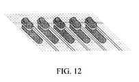
- FIG. 12is a more accurate pictorial view of the device shown in FIGS. 10 and 11 .
- FIG. 13is partial plan view of a membrane assembly and a probe card.
- FIG. 14Ais a partial pictorial view of the traces of a membrane assembly.
- FIG. 14Bis a partial plan view of the interconnection between a membrane assembly and a probe card.
- FIG. 14Cis a partial sectional side view of the interconnection between the membrane assembly and the probe card of FIG. 14 B.
- FIG. 15is a partial sectional view of a probe card illustrating the leakage currents from the end portions of the signal and guard conductors.
- FIG. 16is a partial sectional view of a probe card illustrating the interconnecting of a pair of guard conductors together with a signal conductor therebetween.
- FIG. 17is a partial plan view of a portion of a probe card illustrating power conductors, signal conductors, force conductors, sense conductors, removed interconnecting portions, and interconnected guard conductors.
- FIGS. 18A-18Dis a partial plan view of a portion of a membrane assembly illustrating signal conductors, force conductors, sense conductors, and interconnected guard conductors.
- FIG. 19is a partial plan view of a probe card and a membrane assembly suitable for a Kelvin connection.
- FIG. 20is a partial plan view of a probe card illustrating different geometries for the interconnection to a membrane assembly.
- FIG. 21is a partial plan view of a membrane assembly illustrating a guard conductor looping around a respective probing device.
- FIGS. 22A-22Cis a plan view of a “pogo-pin” probe card constructed in accordance with aspects of the present invention, where the connections to the probe card are normally electrical contacts from a probe ahead positioned above the probe card.
- probe card designershave been concerned with developing techniques for controlling(e.g., minimizing) leakage currents.
- Unwanted currents that flow into a particular cable (or conductor)from surrounding cables (or conductors)may distort the current measured in that particular cable (or conductor).
- the amount of leakage current that will flow between themwill vary depending upon the volume resistivity of the insulating material that separates the conductors. In other words, if a relatively lower-resistance insulator is used, this will result in a relatively higher leakage current.
- One technique that has been used for suppressing inter-channel leakage currentsis positioning the signal conductor between a pair of guard conductors, where each guard conductor is maintained at the same potential as the signal conductor by a feedback circuit in the output channel of the test instrument. Because the voltage potentials of the guard conductors and the respective signal conductor are made to substantially track each other, negligible leakage current will flow from the signal conductor to the corresponding guard conductors. Although leakage current can still flow between different sets of guard conductors, this is typically not a problem because the guard conductors, unlike the signal conductors, are at low impedance. By using this guarding technique, significant improvements may be realized in the low-level current measuring capability of certain probe card designs by reducing the capacitance between signal and guard, and increasing the resistance between signal and guard.
- the membrane assemblyis constructed so as to likewise minimize leakage currents between the individual probing devices.
- this minimizationinvolves the selection of membrane materials and likewise providing limited guarding of the signal conductor by a pair of guard conductors to a location proximate the probing device.
- each respective signal conductor 200is located between a pair of respective guard conductors 202 , 204 on the probe card 52 , and the membrane assembly 72 likewise has a matching set of signal conductors 206 and guard conductors 208 , 210 .
- the probe card or the interconnecting linescan serve as pickup sites for ac fields, which ac fields can be rectified by the input circuit of the test instrument so as to cause errors in the indicated dc values.
- each conductive path of the membraneis normally encapsulated within at least one layer of material ( FIG. 14A illustrates multiple conductive paths without additional membrane materials).
- Thisprovides a structure for routing conductive paths, such as the signal and guard conductors, to a location proximate the probing device without being on the exterior (lower surface) of the membrane assembly which may result in inadvertent contact with the device under test.
- conductive pathssuch as the signal and guard conductors
- FIGS. 14B-14Cthe signal and guard lines are actually interconnected between the probe card 52 and the membrane assembly 72 by conductive structures 220 that pass through the outer layer 222 of the membrane assembly 72 to the interior conductive paths 206 , 208 , 210 of the membrane assembly 72 .
- the probe card 52 and membrane assembly 72are mechanically aligned, and accordingly respective conductive structures 220 of the membrane assembly 72 are interconnected with the conductors 200 , 202 , 204 of the probe card 52 .
- the present inventorscame the realization that this extension of the signal and/or guard conductors beyond the location of electrical connection results in significant additional leakage paths.
- the region 216 beyond the end of the guard conductorsprovides for surface leakage paths 218 , which are primarily DC in nature with the characteristic of an added resistance between the respective conductive paths. This surface leakage path from a signal conductor around the end of the adjacent guard conductors reduces the accuracy of measurements by increasing the leakage currents.
- the present inventorslikewise realized that the region 216 beyond the end of the guard conductors provides for a bulk leakage path, which is primarily AC (e.g., not DC) in nature with the characteristic of an added capacitance, between the signal conductor and the conductors beyond the adjacent guard conductors.
- This bulk leakage path from the signal conductor around the end of the adjacent guard conductorsreduces the accuracy of measurements by increasing the leakage currents.
- the guard conductorsin effect, impose a guard voltage into the bulk of the probe card in a region generally underneath the respective guard conductor. This reduces the bulk capacitive leakage currents from the interposed signal conductor in regions with an adjacent guard conductor.
- the opening 230 into which the membrane assembly 72 is supportedincludes a conductive surface 232 therein (e.g., guard, shield, ground) to further isolate the membrane assembly 72 from the probe card 52 .
- a conductive surface 232e.g., guard, shield, ground
- the conductive surface 232results in significant fringe fields 234 (on the surface and in the bulk of the probe card 52 ) at the end of the signal conductors 200 and guard conductors 202 , 204 .
- These fringe fields 234appear to the measuring device as an additional parallel capacitance and resistance. This fringe leakage path at the end of the guard and signal conductors 200 , 202 , 204 reduces the accuracy of measurements by increasing the leakage currents.
- the width of the conductors of the membrane assembly 72 and the probe card 52may be decreased together with the spacing between the conductors. While decreasing the size of the conductor increases the number of interconnections for a given circumferential edge, this unfortunately results in an increased difficultly of aligning the respective conductive traces together. Further, the greater density increases the manufacturing expense of the device.
- the membrane assembly 72is suitable for a higher density of conductive paths than the probe card 52 . Accordingly, the initial limit to the number of interconnects is the ability to fabricate an increasingly greater number of conductive traces on the probe card 52 .
- the interconnecting portion 240 for each respective pair of guard conductorsis preferably on the same plane, such as the top surface of the probe card 52 , together with the guard conductors and signal conductors.
- the interconnecting portion 240reduces the surface leakage path from the signal conductor by interposing a guarded path around the end of the signal conductor.
- the interconnecting portion 240likewise decreases the bulk leakage path from a signal conductor by imposing a guard voltage in a region of the bulk of the probe card completely enclosing the end of the signal conductor. Also, the fringe leakage path to the central conductive surface 232 from the end of the signal conductor is substantially reduced, or otherwise eliminated, by providing the guarded interconnecting portion 240 around the end of the signal conductor. Reducing the leakage currents by including the additional interconnecting guard portion 240 results in the measurements made from the measuring device to be more accurate because less leakage currents are erroneously included in the measurements. In addition, a decrease in the settling time of the signals is achieved which reduces the time required to obtain a set of accurate measurements.
- One or more of the aforementioned drawbacks and/or advantagesmay be present and/or achieved depending upon the particular device and implementation.
- the interconnecting portion 240electrically interconnecting together a pair of guard conductors 202 , 204 another benefit is more achievable, namely, increasing the number of potential interconnections, without necessarily changing the size of the membrane assembly 72 , without: necessarily changing the geometry of the individual conductors, and without necessarily decreasing the spacing between adjacent conductors.
- the contacting region 250 for the contacts 220 of the membrane assembly 72 on the probe card 52are provided on at least one side of the interconnected guard conductor 202 , 204 , 240 . This permits easier alignment of the membrane assembly 72 and the probe card 52 .
- the width of the guard conductor on the side generally opposite the contacting regionmay be considerably thinner because there is no contact by the membrane assembly 72 with that portion of the guard conductor.
- the different widths of the guard conductors proximate the end of the signal conductorpermits a greater density of conductors to be achieved, if desired, without decreasing the mechanical tolerances required.
- a pair of contactsmay be used, if desired. As a result, the density of the interconnect between the probe card 52 and the membrane assembly 72 is closer to the capability of the membrane assembly 72 .
- the guard conductors of the membrane assembly 72preferably include an interconnecting guard portion 260 with the inderdisposed signal conductor, in a manner similar to the interconnecting guard portion 240 .
- the interconnecting membrane guard portion 260provides many of the same advantages as described above with respect to the interconnecting probe guard portion 240 . By including the interconnecting membrane guard portion 260 , only a single conductive structure 220 needs to be provided between the membrane assembly 72 and the probe card 52 for each set of guard conductors.
- a “true Kelvin” connectionis constructed. This involves using what is generally referred to as a force signal and a sense signal.
- the signal conductor from one of the two conductorsis considered the force conductor, while the signal conductor from the other of the two conductors is considered the sense conductor.
- the force conductoris brought into contact with a test pad on the wafer.
- the force conductoris a low impedance connection, so a current is forced through the force conductor for testing purposes.
- the sense conductoris a high impedance connection and is also brought into contact with the same test pad (or a different test pad) on the wafer, preferably in close proximity to the sense conductor, in order to sense the voltage. As such the current versus voltage characteristics of the test device can be obtained using the force and sense conductors.
- one potential technique to achieve a Kelvin connection with the membrane probing systemis to design the probe card 52 to include multiple sets of a force conductor, a sense conductor, and a corresponding pair of guard connectors on opposing sides of the force/sense conductors (preferably with the interconnection portion).
- the membrane assembly 72likewise includes corresponding sets of a force conductor, a sense conductor, and guard conductors (preferably with the interconnecting portion).
- Thisprovides a potential technique for achieving a Kelvin connection but unfortunately this wastes interconnection space on the probe card 52 in the event that a Kelvin connection for any particular device under test is not necessary.
- the probe card 52may be redesigned for each membrane probing assembly, which is typically unique for each application. However, redesigning the probe card 52 for each application is expensive and not generally an acceptable solution.
- the present inventorsWhile considering how to maintain one or more standard probe cards 52 , together with providing Kelvin connections for each line, the present inventors initially observed that the probe card 52 has more available surface area for routing the conductors further from the interconnection between the probe card 52 and the membrane assembly 72 . With the additional surface area at regions not proximate the interconnection between the probe card 52 and the membrane assembly 72 , a pair of conductive traces 280 , 282 are easily routed, the pair being located between a pair of guard conductors 284 , 286 , to a location generally proximate the interconnection (see FIG. 17 ). For non-Kelvin measurements, one of the conductors may be used as the signal line with the remaining interconnected conductor not used.
- the interconnection 270 between the two interconnected signal conductorsmay be removed (open-circuited) for low noise measurements.
- the two signal conductorse.g. force and sense
- the interconnection portionmay be maintained and one of the pair of conductors 280 , 282 would be used as a force conductor and the other conductor of the pair would be used as a sense conductor.
- Quasi-Kelvin connectionsare generally formed by the interconnection of a sense conductor and a force conductor at a point before the device under test.
- typically low impedance power conductors 300are provided on the probe card 52 to supply power to the probing devices of the membrane assembly 72 .
- the present inventorsdetermined that the interconnection 270 between the pair of conductors may be removed and the force conductor 280 may be jumpered with a wire bond 302 (or any other suitable technique) to an unused power conductor on the probe card 52 .
- Each of the power conductors 300 on the probe card 52are preferably conductive members within the bulk of the probe card 52 , electrically connected to the surface of the probe card 52 by using a set of vias 304 , 306 .
- Each power conductoris routed to a location proximate the interconnection between the probe card 52 and the membrane assembly 72 .
- the power conductoris normally a low impedance conductor. Because the force conductor is a low-impedance connection designed to carry significant current it is preferable to locate the force conductor outside of the guards 284 , 286 of its corresponding sense conductor. In addition, because the force conductor is a low-impedance path carrying significant (non-negligible) current levels it does not necessarily require the guarding provided by the guard conductors 284 , 286 on opposing sides of the sense conductor 282 .
- the power conductorsto which force conductors may be interconnected with, are preferably routed within the bulk of the probe card 52 in a region directly underneath the corresponding sense conductor.
- the conductive power conductorprovides additional protection for the sense conductor to minimize leakage currents.
- the power conductormay be routed on the top surface (or bottom surface) of the probe card, if desired.
- the power conductoris preferably routed to a point “interior” to the end of the corresponding signal conductor using a “via” 306 to the upper surface of the probe card 52 . Accordingly, the power conductor is available at a location suitable for interconnection to the membrane assembly 72 , if desired, while likewise being available for interconnection as a force conductor. In this manner, the same power conductor may be used to provide power to the device under test, while likewise providing a force connection, both of which in a manner that maintains the density of the interconnection of the interface between the probe card 52 and the membrane assembly 72 . The actual use of the power conductors depends on the application and the particular design of the membrane assembly 72 .
- Another technique suitable to provide a greater density of interconnects, and their corresponding interconnecting regionsis to align the interconnects of the probe card 52 in a non-linear fashion (e.g., some closer and some farther from the edge of the probe card 52 ) around the circumference of the membrane assembly 72 , as shown in FIG. 20.
- a further technique suitable to provide a greater density of interconnectsis to align the interconnecting regions in an overlapping manner with respect to a direction perpendicular to the adjacent membrane assembly 72 .
- the membrane assembly 72would likewise have corresponding structures suitable to interconnect to the two-dimensional structure of the conductors of the probe card 52 .
- the present inventorscame to the realization that the membrane assembly is susceptible to absorption of moisture which increases the leakage currents within the membrane assembly.
- FIG. 21another structure suitable to reduce leakage currents for the probing devices is shown.
- the guarded conductors 310 of the membrane assembly 72encircle the end of the probing device 312 , with the signal conductor connected thereto 314 .
- the guarded conductors 310are within the bulk of the membrane assembly 72 to prevent their inadvertent contact with the device under test. Providing the guarded probing devices significantly reduces the effects of leakage currents between the probing devices, especially due to the effects of humidity.
- the present inventorsdetermined that the surface leakage currents between adjacent probing devices may be reduced by removing at least a portion of the membrane material (dielectric) 316 in a location proximate a portion of the guard conductors 310 and between the probing devices 312 . In this manner, a portion of the guard conductor 310 will be exposed to the surface, albeit somewhat recessed from the surface of the membrane assembly 72 , thereby impeding the passage of surface leakage between probing devices 312 .
- a pogo pin probe cardin one embodiment of the present invention includes guarded signal paths and is suitable for receiving a progo pin probe head for connection thereto.
Landscapes
- Physics & Mathematics (AREA)
- General Physics & Mathematics (AREA)
- Engineering & Computer Science (AREA)
- Computer Hardware Design (AREA)
- Microelectronics & Electronic Packaging (AREA)
- General Engineering & Computer Science (AREA)
- Measuring Leads Or Probes (AREA)
- Testing Or Measuring Of Semiconductors Or The Like (AREA)
- Testing Of Individual Semiconductor Devices (AREA)
Abstract
Description
Claims (36)
Priority Applications (7)
| Application Number | Priority Date | Filing Date | Title |
|---|---|---|---|
| US09/637,527US6838890B2 (en) | 2000-02-25 | 2000-11-29 | Membrane probing system |
| PCT/US2001/005430WO2001063308A1 (en) | 2000-02-25 | 2001-02-20 | Membrane probing system |
| AU2001238550AAU2001238550A1 (en) | 2000-02-25 | 2001-02-20 | Membrane probing system |
| US10/909,229US6930498B2 (en) | 2000-02-25 | 2004-07-29 | Membrane probing system |
| US11/144,852US7148711B2 (en) | 2000-02-25 | 2005-06-03 | Membrane probing system |
| US11/509,176US7403025B2 (en) | 2000-02-25 | 2006-08-23 | Membrane probing system |
| US12/214,001US20080252316A1 (en) | 2000-02-25 | 2008-06-16 | Membrane probing system |
Applications Claiming Priority (2)
| Application Number | Priority Date | Filing Date | Title |
|---|---|---|---|
| US18485100P | 2000-02-25 | 2000-02-25 | |
| US09/637,527US6838890B2 (en) | 2000-02-25 | 2000-11-29 | Membrane probing system |
Related Child Applications (1)
| Application Number | Title | Priority Date | Filing Date |
|---|---|---|---|
| US10/909,229ContinuationUS6930498B2 (en) | 2000-02-25 | 2004-07-29 | Membrane probing system |
Publications (2)
| Publication Number | Publication Date |
|---|---|
| US20030132767A1 US20030132767A1 (en) | 2003-07-17 |
| US6838890B2true US6838890B2 (en) | 2005-01-04 |
Family
ID=26880533
Family Applications (5)
| Application Number | Title | Priority Date | Filing Date |
|---|---|---|---|
| US09/637,527Expired - LifetimeUS6838890B2 (en) | 2000-02-25 | 2000-11-29 | Membrane probing system |
| US10/909,229Expired - Fee RelatedUS6930498B2 (en) | 2000-02-25 | 2004-07-29 | Membrane probing system |
| US11/144,852Expired - Fee RelatedUS7148711B2 (en) | 2000-02-25 | 2005-06-03 | Membrane probing system |
| US11/509,176Expired - Fee RelatedUS7403025B2 (en) | 2000-02-25 | 2006-08-23 | Membrane probing system |
| US12/214,001AbandonedUS20080252316A1 (en) | 2000-02-25 | 2008-06-16 | Membrane probing system |
Family Applications After (4)
| Application Number | Title | Priority Date | Filing Date |
|---|---|---|---|
| US10/909,229Expired - Fee RelatedUS6930498B2 (en) | 2000-02-25 | 2004-07-29 | Membrane probing system |
| US11/144,852Expired - Fee RelatedUS7148711B2 (en) | 2000-02-25 | 2005-06-03 | Membrane probing system |
| US11/509,176Expired - Fee RelatedUS7403025B2 (en) | 2000-02-25 | 2006-08-23 | Membrane probing system |
| US12/214,001AbandonedUS20080252316A1 (en) | 2000-02-25 | 2008-06-16 | Membrane probing system |
Country Status (3)
| Country | Link |
|---|---|
| US (5) | US6838890B2 (en) |
| AU (1) | AU2001238550A1 (en) |
| WO (1) | WO2001063308A1 (en) |
Cited By (18)
| Publication number | Priority date | Publication date | Assignee | Title |
|---|---|---|---|---|
| US20030090278A1 (en)* | 2001-08-21 | 2003-05-15 | Kenneth Smith | Membrane probing system |
| US20040196059A1 (en)* | 2003-04-07 | 2004-10-07 | Gabriel Martin J. | Variable inductance test socket and method of manufacturing using such a test socket |
| US20050046433A1 (en)* | 2003-08-25 | 2005-03-03 | Valts Treibergs | Integrated printed circuit board and test contactor for high speed semiconductor testing |
| US20070245536A1 (en)* | 1998-07-14 | 2007-10-25 | Cascade Microtech,, Inc. | Membrane probing system |
| US20080054927A1 (en)* | 2006-08-22 | 2008-03-06 | Kabushiki Kaisha Nihon Micronics | Probe assembly |
| US20080157795A1 (en)* | 2004-07-07 | 2008-07-03 | Cascade Microtech, Inc. | Probe head having a membrane suspended probe |
| US7403025B2 (en) | 2000-02-25 | 2008-07-22 | Cascade Microtech, Inc. | Membrane probing system |
| US7533462B2 (en) | 1999-06-04 | 2009-05-19 | Cascade Microtech, Inc. | Method of constructing a membrane probe |
| US7541821B2 (en) | 1996-08-08 | 2009-06-02 | Cascade Microtech, Inc. | Membrane probing system with local contact scrub |
| US20100085069A1 (en)* | 2008-10-06 | 2010-04-08 | Smith Kenneth R | Impedance optimized interface for membrane probe application |
| US20100127725A1 (en)* | 2008-11-21 | 2010-05-27 | Smith Kenneth R | Replaceable coupon for a probing apparatus |
| WO2015130573A1 (en)* | 2014-02-25 | 2015-09-03 | Cascade Microtech, Inc. | Systems and methods for on-wafer dynamic testing of electronic devices |
| US9435855B2 (en) | 2013-11-19 | 2016-09-06 | Teradyne, Inc. | Interconnect for transmitting signals between a device and a tester |
| US9594114B2 (en) | 2014-06-26 | 2017-03-14 | Teradyne, Inc. | Structure for transmitting signals in an application space between a device under test and test electronics |
| US9977052B2 (en) | 2016-10-04 | 2018-05-22 | Teradyne, Inc. | Test fixture |
| US10677815B2 (en) | 2018-06-08 | 2020-06-09 | Teradyne, Inc. | Test system having distributed resources |
| US11363746B2 (en) | 2019-09-06 | 2022-06-14 | Teradyne, Inc. | EMI shielding for a signal trace |
| US11862901B2 (en) | 2020-12-15 | 2024-01-02 | Teradyne, Inc. | Interposer |
Families Citing this family (27)
| Publication number | Priority date | Publication date | Assignee | Title |
|---|---|---|---|---|
| US6232789B1 (en) | 1997-05-28 | 2001-05-15 | Cascade Microtech, Inc. | Probe holder for low current measurements |
| DE20114544U1 (en) | 2000-12-04 | 2002-02-21 | Cascade Microtech, Inc., Beaverton, Oreg. | wafer probe |
| EP1329730A1 (en)* | 2002-01-17 | 2003-07-23 | Siemens Aktiengesellschaft | Eddy current probe on a flexible substrat |
| KR100864916B1 (en) | 2002-05-23 | 2008-10-22 | 캐스케이드 마이크로테크 인코포레이티드 | Probes for Testing Devices Under Test |
| US6724205B1 (en) | 2002-11-13 | 2004-04-20 | Cascade Microtech, Inc. | Probe for combined signals |
| US7057404B2 (en) | 2003-05-23 | 2006-06-06 | Sharp Laboratories Of America, Inc. | Shielded probe for testing a device under test |
| WO2005065258A2 (en) | 2003-12-24 | 2005-07-21 | Cascade Microtech, Inc. | Active wafer probe |
| EP1789812A2 (en) | 2004-09-13 | 2007-05-30 | Cascade Microtech, Inc. | Double sided probing structures |
| US7656172B2 (en) | 2005-01-31 | 2010-02-02 | Cascade Microtech, Inc. | System for testing semiconductors |
| US7535247B2 (en) | 2005-01-31 | 2009-05-19 | Cascade Microtech, Inc. | Interface for testing semiconductors |
| US7449899B2 (en) | 2005-06-08 | 2008-11-11 | Cascade Microtech, Inc. | Probe for high frequency signals |
| JP5080459B2 (en) | 2005-06-13 | 2012-11-21 | カスケード マイクロテック インコーポレイテッド | Wideband active / passive differential signal probe |
| TWI298794B (en)* | 2006-02-15 | 2008-07-11 | Via Tech Inc | Plunger and chip-testing module applying the same |
| US7609077B2 (en) | 2006-06-09 | 2009-10-27 | Cascade Microtech, Inc. | Differential signal probe with integral balun |
| US7764072B2 (en) | 2006-06-12 | 2010-07-27 | Cascade Microtech, Inc. | Differential signal probing system |
| US7403028B2 (en) | 2006-06-12 | 2008-07-22 | Cascade Microtech, Inc. | Test structure and probe for differential signals |
| US7443186B2 (en) | 2006-06-12 | 2008-10-28 | Cascade Microtech, Inc. | On-wafer test structures for differential signals |
| US7723999B2 (en) | 2006-06-12 | 2010-05-25 | Cascade Microtech, Inc. | Calibration structures for differential signal probing |
| US8130005B2 (en)* | 2006-12-14 | 2012-03-06 | Formfactor, Inc. | Electrical guard structures for protecting a signal trace from electrical interference |
| WO2008120302A1 (en)* | 2007-03-28 | 2008-10-09 | Fujitsu Microelectronics Limited | Test device for semiconductor device |
| US7876114B2 (en) | 2007-08-08 | 2011-01-25 | Cascade Microtech, Inc. | Differential waveguide probe |
| US8622752B2 (en)* | 2011-04-13 | 2014-01-07 | Teradyne, Inc. | Probe-card interposer constructed using hexagonal modules |
| US8917106B2 (en)* | 2011-11-09 | 2014-12-23 | Advantest America, Inc. | Fine pitch microelectronic contact array and method of making same |
| SG11201610578WA (en) | 2014-06-20 | 2017-01-27 | Xcerra Corp | Test socket assembly and related methods |
| TWI652484B (en) | 2018-03-06 | 2019-03-01 | 均豪精密工業股份有限公司 | Probe card on line needle tuning repair system and method thereof |
| CN112444724A (en)* | 2019-09-05 | 2021-03-05 | 英业达科技有限公司 | Test equipment |
| TWI712809B (en)* | 2019-09-10 | 2020-12-11 | 英業達股份有限公司 | Testing apparatus |
Citations (77)
| Publication number | Priority date | Publication date | Assignee | Title |
|---|---|---|---|---|
| US3401126A (en) | 1965-06-18 | 1968-09-10 | Ibm | Method of rendering noble metal conductive composition non-wettable by solder |
| US3429040A (en) | 1965-06-18 | 1969-02-25 | Ibm | Method of joining a component to a substrate |
| US3541222A (en) | 1969-01-13 | 1970-11-17 | Bunker Ramo | Connector screen for interconnecting adjacent surfaces of laminar circuits and method of making |
| US3596228A (en) | 1969-05-29 | 1971-07-27 | Ibm | Fluid actuated contactor |
| US3634807A (en) | 1969-03-28 | 1972-01-11 | Siemens Ag | Detachable electrical contact arrangement |
| US3654585A (en) | 1970-03-11 | 1972-04-04 | Brooks Research And Mfg Inc | Coordinate conversion for the testing of printed circuit boards |
| US3680037A (en) | 1970-11-05 | 1972-07-25 | Tech Wire Prod Inc | Electrical interconnector |
| US3806801A (en) | 1972-12-26 | 1974-04-23 | Ibm | Probe contactor having buckling beam probes |
| US3839672A (en)* | 1973-02-05 | 1974-10-01 | Belden Corp | Method and apparatus for measuring the effectiveness of the shield in a coaxial cable |
| US3862790A (en) | 1971-07-22 | 1975-01-28 | Plessey Handel Investment Ag | Electrical interconnectors and connector assemblies |
| US3971610A (en) | 1974-05-10 | 1976-07-27 | Technical Wire Products, Inc. | Conductive elastomeric contacts and connectors |
| US4027935A (en) | 1976-06-21 | 1977-06-07 | International Business Machines Corporation | Contact for an electrical contactor assembly |
| US4038599A (en) | 1974-12-30 | 1977-07-26 | International Business Machines Corporation | High density wafer contacting and test system |
| US4184729A (en) | 1977-10-13 | 1980-01-22 | Bunker Ramo Corporation | Flexible connector cable |
| US4581679A (en) | 1983-05-31 | 1986-04-08 | Trw Inc. | Multi-element circuit construction |
| US4636722A (en) | 1984-05-21 | 1987-01-13 | Probe-Rite, Inc. | High density probe-head with isolated and shielded transmission lines |
| US4636772A (en) | 1985-01-17 | 1987-01-13 | Riken Denshi Co. Ltd. | Multiple function type D/A converter |
| US4649339A (en) | 1984-04-25 | 1987-03-10 | Honeywell Inc. | Integrated circuit interface |
| US4663840A (en) | 1984-12-11 | 1987-05-12 | U.S. Philips Corporation | Method of interconnecting conductors of different layers of a multilayer printed circuit board |
| EP0230348A2 (en) | 1986-01-07 | 1987-07-29 | Hewlett-Packard Company | Test probe |
| US4707657A (en) | 1984-06-13 | 1987-11-17 | Boegh Petersen Allan | Connector assembly for a circuit board testing machine, a circuit board testing machine, and a method of testing a circuit board by means of a circuit board testing machine |
| EP0259163A2 (en) | 1986-09-05 | 1988-03-09 | Tektronix, Inc. | Semiconductor wafer probe |
| US4793814A (en) | 1986-07-21 | 1988-12-27 | Rogers Corporation | Electrical circuit board interconnect |
| US4837507A (en) | 1984-06-08 | 1989-06-06 | American Telephone And Telegraph Company At&T Technologies, Inc. | High frequency in-circuit test fixture |
| US4906920A (en) | 1988-10-11 | 1990-03-06 | Hewlett-Packard Company | Self-leveling membrane probe |
| US4912399A (en)* | 1987-06-09 | 1990-03-27 | Tektronix, Inc. | Multiple lead probe for integrated circuits in wafer form |
| US4918383A (en) | 1987-01-20 | 1990-04-17 | Huff Richard E | Membrane probe with automatic contact scrub action |
| US4922192A (en) | 1988-09-06 | 1990-05-01 | Unisys Corporation | Elastic membrane probe |
| US4975638A (en) | 1989-12-18 | 1990-12-04 | Wentworth Laboratories | Test probe assembly for testing integrated circuit devices |
| US4980637A (en) | 1988-03-01 | 1990-12-25 | Hewlett-Packard Company | Force delivery system for improved precision membrane probe |
| US4987100A (en) | 1988-05-26 | 1991-01-22 | International Business Machines Corporation | Flexible carrier for an electronic device |
| US4991290A (en) | 1988-07-21 | 1991-02-12 | Microelectronics And Computer Technology | Flexible electrical interconnect and method of making |
| US5020219A (en) | 1988-05-16 | 1991-06-04 | Leedy Glenn J | Method of making a flexible tester surface for testing integrated circuits |
| US5059898A (en) | 1990-08-09 | 1991-10-22 | Tektronix, Inc. | Wafer probe with transparent loading member |
| US5061192A (en) | 1990-12-17 | 1991-10-29 | International Business Machines Corporation | High density connector |
| US5069628A (en) | 1990-03-13 | 1991-12-03 | Hughes Aircraft Company | Flexible electrical cable connector with double sided dots |
| US5097101A (en) | 1991-02-05 | 1992-03-17 | Tektronix, Inc. | Method of forming a conductive contact bump on a flexible substrate and a flexible substrate |
| US5126286A (en) | 1990-10-05 | 1992-06-30 | Micron Technology, Inc. | Method of manufacturing edge connected semiconductor die |
| US5133119A (en) | 1991-02-28 | 1992-07-28 | Hewlett-Packard Company | Shearing stress interconnection apparatus and method |
| US5134365A (en) | 1989-07-11 | 1992-07-28 | Nihon Denshizairyo Kabushiki Kaisha | Probe card in which contact pressure and relative position of each probe end are correctly maintained |
| US5172050A (en) | 1991-02-15 | 1992-12-15 | Motorola, Inc. | Micromachined semiconductor probe card |
| US5177438A (en) | 1991-08-02 | 1993-01-05 | Motorola, Inc. | Low resistance probe for semiconductor |
| US5180977A (en) | 1991-12-02 | 1993-01-19 | Hoya Corporation Usa | Membrane probe contact bump compliancy system |
| DE4223658A1 (en) | 1991-07-18 | 1993-01-21 | Gold Star Electronics | Test appts. for semiconductor chips with relatively many connectors - uses tape automated bonding band with adhesive surface for connecting lines to test card and dendritically grown metal test points |
| US5207585A (en) | 1990-10-31 | 1993-05-04 | International Business Machines Corporation | Thin interface pellicle for dense arrays of electrical interconnects |
| US5225037A (en) | 1991-06-04 | 1993-07-06 | Texas Instruments Incorporated | Method for fabrication of probe card for testing of semiconductor devices |
| US5293175A (en) | 1991-07-19 | 1994-03-08 | Conifer Corporation | Stacked dual dipole MMDS feed |
| US5313157A (en)* | 1990-10-31 | 1994-05-17 | Hughes Aircraft Company | Probe for jesting an electrical circuit chip |
| US5355079A (en) | 1993-01-07 | 1994-10-11 | Wentworth Laboratories, Inc. | Probe assembly for testing integrated circuit devices |
| US5389885A (en) | 1992-01-27 | 1995-02-14 | Everett Charles Technologies, Inc. | Expandable diaphragm test modules and connectors |
| US5395253A (en) | 1993-04-29 | 1995-03-07 | Hughes Aircraft Company | Membrane connector with stretch induced micro scrub |
| US5412866A (en) | 1993-07-01 | 1995-05-09 | Hughes Aircraft Company | Method of making a cast elastomer/membrane test probe assembly |
| US5453404A (en) | 1992-10-13 | 1995-09-26 | Leedy; Glenn | Method for making an interconnection structure for integrated circuits |
| US5506515A (en) | 1994-07-20 | 1996-04-09 | Cascade Microtech, Inc. | High-frequency probe tip assembly |
| US5517126A (en) | 1993-03-18 | 1996-05-14 | Tokyo Electron Limited | Probe apparatus |
| US5521518A (en) | 1990-09-20 | 1996-05-28 | Higgins; H. Dan | Probe card apparatus |
| US5537372A (en) | 1991-11-15 | 1996-07-16 | International Business Machines Corporation | High density data storage system with topographic contact sensor |
| US5584120A (en) | 1992-02-14 | 1996-12-17 | Research Organization For Circuit Knowledge | Method of manufacturing printed circuits |
| US5589781A (en) | 1990-09-20 | 1996-12-31 | Higgins; H. Dan | Die carrier apparatus |
| US5623214A (en) | 1994-10-14 | 1997-04-22 | Hughes Aircraft Company | Multiport membrane probe for full-wafer testing |
| US5623213A (en) | 1994-09-09 | 1997-04-22 | Micromodule Systems | Membrane probing of circuits |
| WO1998007040A1 (en) | 1996-08-08 | 1998-02-19 | Cascade Microtech, Inc. | Membrane probing system with local contact scrub |
| US5720098A (en) | 1995-05-12 | 1998-02-24 | Probe Technology | Method for making a probe preserving a uniform stress distribution under deflection |
| US5723347A (en) | 1993-09-30 | 1998-03-03 | International Business Machines Corp. | Semi-conductor chip test probe and process for manufacturing the probe |
| US5742174A (en) | 1995-11-03 | 1998-04-21 | Probe Technology | Membrane for holding a probe tip in proper location |
| US5813847A (en) | 1995-10-02 | 1998-09-29 | Abb Research Ltd. | Device and method for injecting fuels into compressed gaseous media |
| US5814847A (en) | 1996-02-02 | 1998-09-29 | National Semiconductor Corp. | General purpose assembly programmable multi-chip package substrate |
| US5869974A (en) | 1996-04-01 | 1999-02-09 | Micron Technology, Inc. | Micromachined probe card having compliant contact members for testing semiconductor wafers |
| US5876082A (en) | 1996-02-15 | 1999-03-02 | Singulus Technologies Gmbh | Device for gripping and holding substrates |
| US5896038A (en) | 1996-11-08 | 1999-04-20 | W. L. Gore & Associates, Inc. | Method of wafer level burn-in |
| US5926029A (en) | 1997-05-27 | 1999-07-20 | International Business Machines Corporation | Ultra fine probe contacts |
| US5973504A (en) | 1994-10-28 | 1999-10-26 | Kulicke & Soffa Industries, Inc. | Programmable high-density electronic device testing |
| US5974662A (en) | 1993-11-16 | 1999-11-02 | Formfactor, Inc. | Method of planarizing tips of probe elements of a probe card assembly |
| US6059982A (en) | 1997-09-30 | 2000-05-09 | International Business Machines Corporation | Micro probe assembly and method of fabrication |
| US6114864A (en) | 1996-04-15 | 2000-09-05 | Nec Corporation | Probe card with plural probe tips on a unitary flexible tongue |
| US6174744B1 (en) | 1995-11-22 | 2001-01-16 | Advantest Corp. | Method of producing micro contact structure and contact probe using same |
| US6256882B1 (en) | 1998-07-14 | 2001-07-10 | Cascade Microtech, Inc. | Membrane probing system |
Family Cites Families (832)
| Publication number | Priority date | Publication date | Assignee | Title |
|---|---|---|---|---|
| US1337866A (en) | 1917-09-27 | 1920-04-20 | Griffiths Ethel Grace | System for protecting electric cables |
| US2142625A (en) | 1932-07-06 | 1939-01-03 | Hollandsche Draad En Kabelfab | High tension cable |
| US2376101A (en) | 1942-04-01 | 1945-05-15 | Ferris Instr Corp | Electrical energy transmission |
| US2389668A (en) | 1943-03-04 | 1945-11-27 | Barnes Drill Co | Indexing mechanism for machine tables |
| US3193712A (en) | 1962-03-21 | 1965-07-06 | Clarence A Harris | High voltage cable |
| US3230299A (en) | 1962-07-18 | 1966-01-18 | Gen Cable Corp | Electrical cable with chemically bonded rubber layers |
| US3445770A (en) | 1965-12-27 | 1969-05-20 | Philco Ford Corp | Microelectronic test probe with defect marker access |
| US3442831A (en) | 1966-04-21 | 1969-05-06 | Borden Co | Vinyl chloride polymerization process and latex |
| US3484679A (en) | 1966-10-03 | 1969-12-16 | North American Rockwell | Electrical apparatus for changing the effective capacitance of a cable |
| US3441315A (en) | 1967-07-07 | 1969-04-29 | Artnell Co | Seat and method for manufacturing the same |
| US3609539A (en) | 1968-09-28 | 1971-09-28 | Ibm | Self-aligning kelvin probe |
| US3595228A (en) | 1968-11-27 | 1971-07-27 | Robert C Simon | Flow line break alarm device |
| US3740900A (en) | 1970-07-01 | 1973-06-26 | Signetics Corp | Vacuum chuck assembly for semiconductor manufacture |
| US3700998A (en) | 1970-08-20 | 1972-10-24 | Computer Test Corp | Sample and hold circuit with switching isolation |
| US3714572A (en) | 1970-08-21 | 1973-01-30 | Rca Corp | Alignment and test fixture apparatus |
| US3710251A (en) | 1971-04-07 | 1973-01-09 | Collins Radio Co | Microelectric heat exchanger pedestal |
| US3829076A (en) | 1972-06-08 | 1974-08-13 | H Sofy | Dial index machine |
| US3858212A (en) | 1972-08-29 | 1974-12-31 | L Tompkins | Multi-purpose information gathering and distribution system |
| US3952156A (en) | 1972-09-07 | 1976-04-20 | Xerox Corporation | Signal processing system |
| CA970849A (en) | 1972-09-18 | 1975-07-08 | Malcolm P. Macmartin | Low leakage isolating transformer for electromedical apparatus |
| JPS5337077Y2 (en) | 1973-08-18 | 1978-09-08 | ||
| US3849728A (en) | 1973-08-21 | 1974-11-19 | Wentworth Labor Inc | Fixed point probe card and an assembly and repair fixture therefor |
| US3936743A (en) | 1974-03-05 | 1976-02-03 | Electroglas, Inc. | High speed precision chuck assembly |
| JPS5352354Y2 (en) | 1974-05-23 | 1978-12-14 | ||
| US3976959A (en) | 1974-07-22 | 1976-08-24 | Gaspari Russell A | Planar balun |
| US3970934A (en) | 1974-08-12 | 1976-07-20 | Akin Aksu | Printed circuit board testing means |
| JPS5750068Y2 (en) | 1974-10-31 | 1982-11-02 | ||
| JPS5166893U (en) | 1974-11-22 | 1976-05-26 | ||
| US4038894A (en) | 1975-07-18 | 1977-08-02 | Springfield Tool And Die, Inc. | Piercing apparatus |
| JPS567439Y2 (en) | 1975-09-20 | 1981-02-18 | ||
| SE407115B (en) | 1975-10-06 | 1979-03-12 | Kabi Ab | PROCEDURES AND METAL ELECTRODES FOR THE STUDY OF ENZYMATIC AND OTHER BIOCHEMICAL REACTIONS |
| US3992073A (en) | 1975-11-24 | 1976-11-16 | Technical Wire Products, Inc. | Multi-conductor probe |
| US4049252A (en) | 1976-02-04 | 1977-09-20 | Bell Theodore F | Index table |
| US4008900A (en) | 1976-03-15 | 1977-02-22 | John Freedom | Indexing chuck |
| US4099120A (en) | 1976-04-19 | 1978-07-04 | Akin Aksu | Probe head for testing printed circuit boards |
| US4115735A (en) | 1976-10-14 | 1978-09-19 | Faultfinders, Inc. | Test fixture employing plural platens for advancing some or all of the probes of the test fixture |
| US4093988A (en) | 1976-11-08 | 1978-06-06 | General Electric Company | High speed frequency response measurement |
| US4312117A (en) | 1977-09-01 | 1982-01-26 | Raytheon Company | Integrated test and assembly device |
| US4135131A (en) | 1977-10-14 | 1979-01-16 | The United States Of America As Represented By The Secretary Of The Army | Microwave time delay spectroscopic methods and apparatus for remote interrogation of biological targets |
| DE2849119A1 (en) | 1978-11-13 | 1980-05-14 | Siemens Ag | METHOD AND CIRCUIT FOR DAMPING MEASUREMENT, ESPECIALLY FOR DETERMINING THE DAMPING AND / OR GROUP DISTANCE DISTORTION OF A MEASURED OBJECT |
| US4383217A (en) | 1979-01-02 | 1983-05-10 | Shiell Thomas J | Collinear four-point probe head and mount for resistivity measurements |
| JPS55115383A (en) | 1979-02-27 | 1980-09-05 | Mitsubishi Electric Corp | Bias circuit for laser diode |
| US4287473A (en) | 1979-05-25 | 1981-09-01 | The United States Of America As Represented By The United States Department Of Energy | Nondestructive method for detecting defects in photodetector and solar cell devices |
| FI58719C (en) | 1979-06-01 | 1981-04-10 | Instrumentarium Oy | DIAGNOSTISERINGSANORDNING FOER BROESTKANCER |
| US4277741A (en) | 1979-06-25 | 1981-07-07 | General Motors Corporation | Microwave acoustic spectrometer |
| SU843040A1 (en) | 1979-08-06 | 1981-06-30 | Физико-Технический Институт Низкихтемператур Ah Украинской Ccp | Straightway rejection filter |
| US4327180A (en) | 1979-09-14 | 1982-04-27 | Board Of Governors, Wayne State Univ. | Method and apparatus for electromagnetic radiation of biological material |
| US4284033A (en) | 1979-10-31 | 1981-08-18 | Rca Corporation | Means to orbit and rotate target wafers supported on planet member |
| US4330783A (en) | 1979-11-23 | 1982-05-18 | Toia Michael J | Coaxially fed dipole antenna |
| JPS6016996Y2 (en) | 1979-12-10 | 1985-05-25 | 横河電機株式会社 | Address selection device for input/output interface device |
| JPS56134590A (en) | 1980-03-18 | 1981-10-21 | Sumitomo Chemical Co | Manufacture of highly nonstatic ammonium nitrate oil explosive |
| US4284682A (en) | 1980-04-30 | 1981-08-18 | Nasa | Heat sealable, flame and abrasion resistant coated fabric |
| US4357575A (en) | 1980-06-17 | 1982-11-02 | Dit-Mco International Corporation | Apparatus for use in testing printed circuit process boards having means for positioning such boards in proper juxtaposition with electrical contacting assemblies |
| US4552033A (en) | 1980-07-08 | 1985-11-12 | Gebr. Marzhauser Wetzlar oHG | Drive system for a microscope stage or the like |
| JPS6211243Y2 (en) | 1980-09-17 | 1987-03-17 | ||
| JPS5775480U (en) | 1980-10-24 | 1982-05-10 | ||
| US4376920A (en) | 1981-04-01 | 1983-03-15 | Smith Kenneth L | Shielded radio frequency transmission cable |
| JPS6238032Y2 (en) | 1981-04-06 | 1987-09-29 | ||
| US4425395A (en) | 1981-04-30 | 1984-01-10 | Fujikura Rubber Works, Ltd. | Base fabrics for polyurethane-coated fabrics, polyurethane-coated fabrics and processes for their production |
| US4401945A (en) | 1981-04-30 | 1983-08-30 | The Valeron Corporation | Apparatus for detecting the position of a probe relative to a workpiece |
| US4453142A (en) | 1981-11-02 | 1984-06-05 | Motorola Inc. | Microstrip to waveguide transition |
| DE3202461C1 (en) | 1982-01-27 | 1983-06-09 | Fa. Carl Zeiss, 7920 Heidenheim | Attachment of microscope objectives |
| US4468629A (en) | 1982-05-27 | 1984-08-28 | Trw Inc. | NPN Operational amplifier |
| US4528504A (en) | 1982-05-27 | 1985-07-09 | Harris Corporation | Pulsed linear integrated circuit tester |
| US4705447A (en) | 1983-08-11 | 1987-11-10 | Intest Corporation | Electronic test head positioner for test systems |
| SU1392603A1 (en) | 1982-11-19 | 1988-04-30 | Физико-технический институт низких температур АН УССР | Band-rejection filter |
| US4487996A (en) | 1982-12-02 | 1984-12-11 | Electric Power Research Institute, Inc. | Shielded electrical cable |
| JPH0685044B2 (en) | 1983-02-28 | 1994-10-26 | キヤノン株式会社 | Image reproduction output device |
| JPS59226167A (en) | 1983-06-04 | 1984-12-19 | Dainippon Screen Mfg Co Ltd | Surface treating device for circuit board |
| FR2547945B1 (en) | 1983-06-21 | 1986-05-02 | Raffinage Cie Francaise | NEW STRUCTURE OF ELECTRIC CABLE AND ITS APPLICATIONS |
| JPS6071425U (en) | 1983-10-25 | 1985-05-20 | 株式会社アマダ | Mounting structure of upper apron in press machine |
| JPS6060042U (en) | 1983-09-30 | 1985-04-26 | 日本電気ホームエレクトロニクス株式会社 | disk clamp device |
| US4588950A (en) | 1983-11-15 | 1986-05-13 | Data Probe Corporation | Test system for VLSI digital circuit and method of testing |
| JPS60136006U (en) | 1984-02-20 | 1985-09-10 | 株式会社 潤工社 | flat cable |
| US4646005A (en) | 1984-03-16 | 1987-02-24 | Motorola, Inc. | Signal probe |
| US4697143A (en) | 1984-04-30 | 1987-09-29 | Cascade Microtech, Inc. | Wafer probe |
| JPS60235304A (en) | 1984-05-08 | 1985-11-22 | 株式会社フジクラ | DC power cable |
| US4515133A (en) | 1984-05-31 | 1985-05-07 | Frank Roman | Fuel economizing device |
| US4755747A (en) | 1984-06-15 | 1988-07-05 | Canon Kabushiki Kaisha | Wafer prober and a probe card to be used therewith |
| DE3428087A1 (en) | 1984-07-30 | 1986-01-30 | Kraftwerk Union AG, 4330 Mülheim | CONCENTRIC THREE-WIRE CABLE |
| US4593243A (en) | 1984-08-29 | 1986-06-03 | Magnavox Government And Industrial Electronics Company | Coplanar and stripline probe card apparatus |
| US4713347A (en) | 1985-01-14 | 1987-12-15 | Sensor Diagnostics, Inc. | Measurement of ligand/anti-ligand interactions using bulk conductance |
| US4651115A (en) | 1985-01-31 | 1987-03-17 | Rca Corporation | Waveguide-to-microstrip transition |
| US4780670A (en) | 1985-03-04 | 1988-10-25 | Xerox Corporation | Active probe card for high resolution/low noise wafer level testing |
| US4744041A (en) | 1985-03-04 | 1988-05-10 | International Business Machines Corporation | Method for testing DC motors |
| US4691163A (en) | 1985-03-19 | 1987-09-01 | Elscint Ltd. | Dual frequency surface probes |
| US4755746A (en) | 1985-04-24 | 1988-07-05 | Prometrix Corporation | Apparatus and methods for semiconductor wafer testing |
| US4684883A (en) | 1985-05-13 | 1987-08-04 | American Telephone And Telegraph Company, At&T Bell Laboratories | Method of manufacturing high-quality semiconductor light-emitting devices |
| FR2585513B1 (en) | 1985-07-23 | 1987-10-09 | Thomson Csf | COUPLING DEVICE BETWEEN A METAL WAVEGUIDE, A DIELECTRIC WAVEGUIDE AND A SEMICONDUCTOR COMPONENT, AND MIXER USING THE SAME |
| EP0213825A3 (en) | 1985-08-22 | 1989-04-26 | Molecular Devices Corporation | Multiple chemically modulated capacitance |
| DE3531893A1 (en) | 1985-09-06 | 1987-03-19 | Siemens Ag | METHOD FOR DETERMINING THE DISTRIBUTION OF DIELECTRICITY CONSTANTS IN AN EXAMINATION BODY, AND MEASURING ARRANGEMENT FOR IMPLEMENTING THE METHOD |
| US4746857A (en) | 1985-09-13 | 1988-05-24 | Danippon Screen Mfg. Co. Ltd. | Probing apparatus for measuring electrical characteristics of semiconductor device formed on wafer |
| US4749942A (en) | 1985-09-26 | 1988-06-07 | Tektronix, Inc. | Wafer probe head |
| JPH0326643Y2 (en) | 1985-09-30 | 1991-06-10 | ||
| US5917707A (en) | 1993-11-16 | 1999-06-29 | Formfactor, Inc. | Flexible contact structure with an electrically conductive shell |
| US6330164B1 (en) | 1985-10-18 | 2001-12-11 | Formfactor, Inc. | Interconnect assemblies and methods including ancillary electronic component connected in immediate proximity of semiconductor device |
| US5829128A (en) | 1993-11-16 | 1998-11-03 | Formfactor, Inc. | Method of mounting resilient contact structures to semiconductor devices |
| US6043563A (en) | 1997-05-06 | 2000-03-28 | Formfactor, Inc. | Electronic components with terminals and spring contact elements extending from areas which are remote from the terminals |
| US5476211A (en) | 1993-11-16 | 1995-12-19 | Form Factor, Inc. | Method of manufacturing electrical contacts, using a sacrificial member |
| JPH06102313B2 (en) | 1985-10-31 | 1994-12-14 | メドマン株式会社 | Self-aligning mating tool |
| JPS62139000A (en) | 1985-12-12 | 1987-06-22 | 日本電気株式会社 | Frame id check system for telemeter |
| JPS6298634U (en) | 1985-12-12 | 1987-06-23 | ||
| US4853627A (en) | 1985-12-23 | 1989-08-01 | Triquint Semiconductor, Inc. | Wafer probes |
| JPS62107937U (en) | 1985-12-25 | 1987-07-10 | ||
| DE3785681T2 (en) | 1986-01-24 | 1993-08-12 | Fuji Photo Film Co Ltd | SHEET FILM CASSETTE AND DEVICE FOR LOADING SHEET FILMS. |
| JPS62239050A (en) | 1986-04-10 | 1987-10-19 | Kobe Steel Ltd | Eddy current test equipment |
| US4757255A (en) | 1986-03-03 | 1988-07-12 | National Semiconductor Corporation | Environmental box for automated wafer probing |
| US4766384A (en) | 1986-06-20 | 1988-08-23 | Schlumberger Technology Corp. | Well logging apparatus for determining dip, azimuth, and invaded zone conductivity |
| US5095891A (en) | 1986-07-10 | 1992-03-17 | Siemens Aktiengesellschaft | Connecting cable for use with a pulse generator and a shock wave generator |
| DE3625631A1 (en) | 1986-07-29 | 1988-02-04 | Gore W L & Co Gmbh | ELECTROMAGNETIC SHIELDING |
| JP2609232B2 (en) | 1986-09-04 | 1997-05-14 | 日本ヒューレット・パッカード株式会社 | Floating drive circuit |
| US4904933A (en) | 1986-09-08 | 1990-02-27 | Tektronix, Inc. | Integrated circuit probe station |
| US4673839A (en) | 1986-09-08 | 1987-06-16 | Tektronix, Inc. | Piezoelectric pressure sensing apparatus for integrated circuit testing stations |
| DE3637549A1 (en) | 1986-11-04 | 1988-05-11 | Hans Dr Med Rosenberger | Measuring device for testing the dielectric properties of biological tissues |
| US4754239A (en) | 1986-12-19 | 1988-06-28 | The United States Of America As Represented By The Secretary Of The Air Force | Waveguide to stripline transition assembly |
| US4772846A (en) | 1986-12-29 | 1988-09-20 | Hughes Aircraft Company | Wafer alignment and positioning apparatus for chip testing by voltage contrast electron microscopy |
| JPH0625332Y2 (en) | 1987-01-06 | 1994-07-06 | ブラザー工業株式会社 | Printer |
| US4812754A (en) | 1987-01-07 | 1989-03-14 | Tracy Theodore A | Circuit board interfacing apparatus |
| US4727637A (en) | 1987-01-20 | 1988-03-01 | The Boeing Company | Computer aided connector assembly method and apparatus |
| US4827211A (en)* | 1987-01-30 | 1989-05-02 | Cascade Microtech, Inc. | Wafer probe |
| US4711563A (en) | 1987-02-11 | 1987-12-08 | Lass Bennett D | Portable collapsible darkroom |
| JPS63129640U (en) | 1987-02-17 | 1988-08-24 | ||
| US4864227A (en) | 1987-02-27 | 1989-09-05 | Canon Kabushiki Kaisha | Wafer prober |
| JPS63143814U (en) | 1987-03-12 | 1988-09-21 | ||
| US5082627A (en) | 1987-05-01 | 1992-01-21 | Biotronic Systems Corporation | Three dimensional binding site array for interfering with an electrical field |
| JPH07111987B2 (en) | 1987-06-22 | 1995-11-29 | 東京エレクトロン株式会社 | Probe device |
| US4894612A (en)* | 1987-08-13 | 1990-01-16 | Hypres, Incorporated | Soft probe for providing high speed on-wafer connections to a circuit |
| EP0304868A3 (en) | 1987-08-28 | 1990-10-10 | Tektronix Inc. | Multiple lead probe for integrated circuits in wafer form |
| US4755874A (en) | 1987-08-31 | 1988-07-05 | Kla Instruments Corporation | Emission microscopy system |
| US5198752A (en) | 1987-09-02 | 1993-03-30 | Tokyo Electron Limited | Electric probing-test machine having a cooling system |
| US5084671A (en) | 1987-09-02 | 1992-01-28 | Tokyo Electron Limited | Electric probing-test machine having a cooling system |
| JPH0660912B2 (en) | 1987-09-07 | 1994-08-10 | 浜松ホトニクス株式会社 | Voltage detector |
| US4791363A (en) | 1987-09-28 | 1988-12-13 | Logan John K | Ceramic microstrip probe blade |
| US4929893A (en) | 1987-10-06 | 1990-05-29 | Canon Kabushiki Kaisha | Wafer prober |
| US4818383A (en)* | 1987-11-02 | 1989-04-04 | Wang Robert O | Apparatus and method for inspecting and grading samples of grain |
| JP2554669Y2 (en) | 1987-11-10 | 1997-11-17 | 博 寺町 | Rotary positioning device |
| US4859989A (en) | 1987-12-01 | 1989-08-22 | W. L. Gore & Associates, Inc. | Security system and signal carrying member thereof |
| US4891584A (en) | 1988-03-21 | 1990-01-02 | Semitest, Inc. | Apparatus for making surface photovoltage measurements of a semiconductor |
| JPH01214038A (en) | 1988-02-22 | 1989-08-28 | Mitsubishi Electric Corp | probe card |
| JPH06103333B2 (en) | 1988-02-27 | 1994-12-14 | アンリツ株式会社 | High frequency characteristic measuring device |
| US5021186A (en) | 1988-03-25 | 1991-06-04 | Nissan Chemical Industries, Ltd. | Chloroisocyanuric acid composition having storage stability |
| US4839587A (en) | 1988-03-29 | 1989-06-13 | Digital Equipment Corporation | Test fixture for tab circuits and devices |
| US4871964A (en) | 1988-04-12 | 1989-10-03 | G. G. B. Industries, Inc. | Integrated circuit probing apparatus |
| JPH01165968U (en) | 1988-05-10 | 1989-11-21 | ||
| US5354695A (en) | 1992-04-08 | 1994-10-11 | Leedy Glenn J | Membrane dielectric isolation IC fabrication |
| US4983910A (en) | 1988-05-20 | 1991-01-08 | Stanford University | Millimeter-wave active probe |
| US5003253A (en) | 1988-05-20 | 1991-03-26 | The Board Of Trustees Of The Leland Stanford Junior University | Millimeter-wave active probe system |
| JP2634191B2 (en) | 1988-05-24 | 1997-07-23 | 三菱電機株式会社 | Probe card |
| US4831494A (en) | 1988-06-27 | 1989-05-16 | International Business Machines Corporation | Multilayer capacitor |
| JPH075078Y2 (en) | 1988-09-29 | 1995-02-08 | シャープ株式会社 | Image forming apparatus having media cartridge |
| US4893914A (en) | 1988-10-12 | 1990-01-16 | The Micromanipulator Company, Inc. | Test station |
| JPH02191352A (en) | 1988-10-24 | 1990-07-27 | Tokyo Electron Ltd | Probe device |
| US4998062A (en) | 1988-10-25 | 1991-03-05 | Tokyo Electron Limited | Probe device having micro-strip line structure |
| JPH02124469A (en) | 1988-11-01 | 1990-05-11 | Nec Kyushu Ltd | Probe card |
| CA1278106C (en) | 1988-11-02 | 1990-12-18 | Gordon Glen Rabjohn | Tunable microwave wafer probe |
| US4849689A (en) | 1988-11-04 | 1989-07-18 | Cascade Microtech, Inc. | Microwave wafer probe having replaceable probe tip |
| JP2648945B2 (en) | 1988-11-07 | 1997-09-03 | 富士通株式会社 | Method for manufacturing semiconductor device |
| US4904935A (en) | 1988-11-14 | 1990-02-27 | Eaton Corporation | Electrical circuit board text fixture having movable platens |
| US5142224A (en) | 1988-12-13 | 1992-08-25 | Comsat | Non-destructive semiconductor wafer probing system using laser pulses to generate and detect millimeter wave signals |
| US4916398A (en) | 1988-12-21 | 1990-04-10 | Spectroscopy Imaging Systems Corp. | Efficient remote transmission line probe tuning for NMR apparatus |
| US4916002A (en)* | 1989-01-13 | 1990-04-10 | The Board Of Trustees Of The Leland Jr. University | Microcasting of microminiature tips |
| US4922128A (en) | 1989-01-13 | 1990-05-01 | Ibm Corporation | Boost clock circuit for driving redundant wordlines and sample wordlines |
| US5232789A (en) | 1989-03-09 | 1993-08-03 | Mtu Motoren- Und Turbinen-Union Muenchen Gmbh | Structural component with a protective coating having a nickel or cobalt basis and method for making such a coating |
| US5159752A (en) | 1989-03-22 | 1992-11-03 | Texas Instruments Incorporated | Scanning electron microscope based parametric testing method and apparatus |
| JPH0712871Y2 (en) | 1989-03-28 | 1995-03-29 | 北斗工機株式会社 | Grain drying equipment |
| US5304924A (en) | 1989-03-29 | 1994-04-19 | Canon Kabushiki Kaisha | Edge detector |
| US5030907A (en) | 1989-05-19 | 1991-07-09 | Knights Technology, Inc. | CAD driven microprobe integrated circuit tester |
| US5045781A (en) | 1989-06-08 | 1991-09-03 | Cascade Microtech, Inc. | High-frequency active probe having replaceable contact needles |
| US5041782A (en) | 1989-09-20 | 1991-08-20 | Design Technique International, Inc. | Microstrip probe |
| US5166606A (en) | 1989-11-03 | 1992-11-24 | John H. Blanz Company, Inc. | High efficiency cryogenic test station |
| US5097207A (en) | 1989-11-03 | 1992-03-17 | John H. Blanz Company, Inc. | Temperature stable cryogenic probe station |
| US5160883A (en) | 1989-11-03 | 1992-11-03 | John H. Blanz Company, Inc. | Test station having vibrationally stabilized X, Y and Z movable integrated circuit receiving support |
| US5267088A (en) | 1989-11-10 | 1993-11-30 | Asahi Kogaku Kogyo Kabushiki Kaisha | Code plate mounting device |
| JPH03175367A (en) | 1989-12-04 | 1991-07-30 | Sharp Corp | Measuring jig for dc characteristic of semiconductor device |
| US5145552A (en)* | 1989-12-21 | 1992-09-08 | Canon Kabushiki Kaisha | Process for preparing electrical connecting member |
| JP2759116B2 (en) | 1989-12-25 | 1998-05-28 | 東京エレクトロン株式会社 | Heat treatment method and heat treatment apparatus |
| US5089774A (en) | 1989-12-26 | 1992-02-18 | Sharp Kabushiki Kaisha | Apparatus and a method for checking a semiconductor |
| JPH03209737A (en) | 1990-01-11 | 1991-09-12 | Tokyo Electron Ltd | Probe equipment |
| US5066357A (en) | 1990-01-11 | 1991-11-19 | Hewlett-Packard Company | Method for making flexible circuit card with laser-contoured vias and machined capacitors |
| US5298972A (en) | 1990-01-22 | 1994-03-29 | Hewlett-Packard Company | Method and apparatus for measuring polarization sensitivity of optical devices |
| US5001423A (en)* | 1990-01-24 | 1991-03-19 | International Business Machines Corporation | Dry interface thermal chuck temperature control system for semiconductor wafer testing |
| JP2873598B2 (en) | 1990-02-02 | 1999-03-24 | 東芝セラミックス株式会社 | Vacuum chuck for semiconductor wafer |
| US5408189A (en) | 1990-05-25 | 1995-04-18 | Everett Charles Technologies, Inc. | Test fixture alignment system for printed circuit boards |
| US5245292A (en) | 1990-06-12 | 1993-09-14 | Iniziative Marittime 1991, S.R.L. | Method and apparatus for sensing a fluid handling |
| US5198753A (en) | 1990-06-29 | 1993-03-30 | Digital Equipment Corporation | Integrated circuit test fixture and method |
| US5061823A (en) | 1990-07-13 | 1991-10-29 | W. L. Gore & Associates, Inc. | Crush-resistant coaxial transmission line |
| US5187443A (en) | 1990-07-24 | 1993-02-16 | Bereskin Alexander B | Microwave test fixtures for determining the dielectric properties of a material |
| US5569591A (en) | 1990-08-03 | 1996-10-29 | University College Of Wales Aberystwyth | Analytical or monitoring apparatus and method |
| KR0138754B1 (en) | 1990-08-06 | 1998-06-15 | 이노우에 아키라 | Touch sensor unit of probe for testing electric circuit and electric circuit testing apparatus using the touch sensor unit |
| US5363050A (en) | 1990-08-31 | 1994-11-08 | Guo Wendy W | Quantitative dielectric imaging system |
| US5091732A (en) | 1990-09-07 | 1992-02-25 | The United States Of America As Represented By The Secretary Of The Navy | Lightweight deployable antenna system |
| US6037785A (en) | 1990-09-20 | 2000-03-14 | Higgins; H. Dan | Probe card apparatus |
| JPH04130639A (en) | 1990-09-20 | 1992-05-01 | Fuji Electric Co Ltd | Method and device for detecting contact of needle of probe card with wafer |
| US5159267A (en) | 1990-09-28 | 1992-10-27 | Sematech, Inc. | Pneumatic energy fluxmeter |
| GB9021448D0 (en) | 1990-10-03 | 1990-11-14 | Renishaw Plc | Capacitance sensing probe |
| JP2544015Y2 (en) | 1990-10-15 | 1997-08-13 | 株式会社アドバンテスト | IC test equipment |
| JPH04159043A (en) | 1990-10-24 | 1992-06-02 | Hitachi Ltd | vacuum chuck |
| JPH04165361A (en) | 1990-10-30 | 1992-06-11 | Toshiba Corp | Semiconductor processing method |
| JP2588060B2 (en) | 1990-11-30 | 1997-03-05 | 住友シチックス株式会社 | Polishing chuck for semiconductor wafer |
| JP3699349B2 (en) | 1990-12-25 | 2005-09-28 | 日本碍子株式会社 | Wafer adsorption heating device |
| US5280156A (en) | 1990-12-25 | 1994-01-18 | Ngk Insulators, Ltd. | Wafer heating apparatus and with ceramic substrate and dielectric layer having electrostatic chucking means |
| US5107076A (en) | 1991-01-08 | 1992-04-21 | W. L. Gore & Associates, Inc. | Easy strip composite dielectric coaxial signal cable |
| JPH04340248A (en) | 1991-01-22 | 1992-11-26 | Tokyo Electron Yamanashi Kk | Wafer prober |
| US5136237A (en) | 1991-01-29 | 1992-08-04 | Tektronix, Inc. | Double insulated floating high voltage test probe |
| US5233306A (en) | 1991-02-13 | 1993-08-03 | The Board Of Regents Of The University Of Wisconsin System | Method and apparatus for measuring the permittivity of materials |
| DE4109908C2 (en)* | 1991-03-26 | 1994-05-05 | Erich Reitinger | Arrangement for testing semiconductor wafers |
| US5172051A (en) | 1991-04-24 | 1992-12-15 | Hewlett-Packard Company | Wide bandwidth passive probe |
| US5487999A (en) | 1991-06-04 | 1996-01-30 | Micron Technology, Inc. | Method for fabricating a penetration limited contact having a rough textured surface |
| US5686317A (en) | 1991-06-04 | 1997-11-11 | Micron Technology, Inc. | Method for forming an interconnect having a penetration limited contact structure for establishing a temporary electrical connection with a semiconductor die |
| US5233197A (en) | 1991-07-15 | 1993-08-03 | University Of Massachusetts Medical Center | High speed digital imaging microscope |
| US5321352A (en) | 1991-08-01 | 1994-06-14 | Tokyo Electron Yamanashi Limited | Probe apparatus and method of alignment for the same |
| US5321453A (en) | 1991-08-03 | 1994-06-14 | Tokyo Electron Limited | Probe apparatus for probing an object held above the probe card |
| US5404111A (en) | 1991-08-03 | 1995-04-04 | Tokyo Electron Limited | Probe apparatus with a swinging holder for an object of examination |
| US5420516A (en) | 1991-09-20 | 1995-05-30 | Audio Precision, Inc. | Method and apparatus for fast response and distortion measurement |
| US5159264A (en) | 1991-10-02 | 1992-10-27 | Sematech, Inc. | Pneumatic energy fluxmeter |
| US5214243A (en) | 1991-10-11 | 1993-05-25 | Endevco Corporation | High-temperature, low-noise coaxial cable assembly with high strength reinforcement braid |
| US5200585A (en)* | 1991-11-06 | 1993-04-06 | Westinghouse Electric Corp. | Drawout switchgear with improved levering-in mechanism and interlock |
| US5846708A (en) | 1991-11-19 | 1998-12-08 | Massachusetts Institiute Of Technology | Optical and electrical methods and apparatus for molecule detection |
| IL103674A0 (en) | 1991-11-19 | 1993-04-04 | Houston Advanced Res Center | Method and apparatus for molecule detection |
| US5414565A (en) | 1991-11-27 | 1995-05-09 | Sullivan; Mark T. | Tilting kinematic mount |
| US5214374A (en) | 1991-12-12 | 1993-05-25 | Everett/Charles Contact Products, Inc. | Dual level test fixture |
| US5274336A (en) | 1992-01-14 | 1993-12-28 | Hewlett-Packard Company | Capacitively-coupled test probe |
| US5367165A (en)* | 1992-01-17 | 1994-11-22 | Olympus Optical Co., Ltd. | Cantilever chip for scanning probe microscope |
| US5374938A (en) | 1992-01-21 | 1994-12-20 | Sharp Kabushiki Kaisha | Waveguide to microstrip conversion means in a satellite broadcasting adaptor |
| US5202558A (en) | 1992-03-04 | 1993-04-13 | Barker Lynn M | Flexible fiber optic probe for high-pressure shock experiments |
| US5672816A (en) | 1992-03-13 | 1997-09-30 | Park Scientific Instruments | Large stage system for scanning probe microscopes and other instruments |
| US5376790A (en) | 1992-03-13 | 1994-12-27 | Park Scientific Instruments | Scanning probe microscope |
| US5254939A (en) | 1992-03-20 | 1993-10-19 | Xandex, Inc. | Probe card system |
| US5478748A (en) | 1992-04-01 | 1995-12-26 | Thomas Jefferson University | Protein assay using microwave energy |
| DE4211362C2 (en) | 1992-04-04 | 1995-04-20 | Berthold Lab Prof Dr | Device for determining material parameters by microwave measurements |
| TW212252B (en) | 1992-05-01 | 1993-09-01 | Martin Marietta Corp | |
| US5266889A (en)* | 1992-05-29 | 1993-11-30 | Cascade Microtech, Inc. | Wafer probe station with integrated environment control enclosure |
| US5479109A (en) | 1992-06-03 | 1995-12-26 | Trw Inc. | Testing device for integrated circuits on wafer |
| US5345170A (en) | 1992-06-11 | 1994-09-06 | Cascade Microtech, Inc. | Wafer probe station having integrated guarding, Kelvin connection and shielding systems |
| US6380751B2 (en)* | 1992-06-11 | 2002-04-30 | Cascade Microtech, Inc. | Wafer probe station having environment control enclosure |
| JPH0634715A (en) | 1992-07-17 | 1994-02-10 | Mitsubishi Electric Corp | High-frequency band probe head |
| US5292175A (en)* | 1992-09-04 | 1994-03-08 | Babystar | Inflatable child vehicle seat |
| FR2695508B1 (en) | 1992-09-08 | 1994-10-21 | Filotex Sa | Low noise cable. |
| US5227730A (en) | 1992-09-14 | 1993-07-13 | Kdc Technology Corp. | Microwave needle dielectric sensors |
| US5371654A (en) | 1992-10-19 | 1994-12-06 | International Business Machines Corporation | Three dimensional high performance interconnection package |
| US6295729B1 (en) | 1992-10-19 | 2001-10-02 | International Business Machines Corporation | Angled flying lead wire bonding process |
| JPH06132709A (en) | 1992-10-20 | 1994-05-13 | Fujitsu General Ltd | Waveguide / stripline converter |
| US5479108A (en) | 1992-11-25 | 1995-12-26 | David Cheng | Method and apparatus for handling wafers |
| JPH06151532A (en) | 1992-11-13 | 1994-05-31 | Tokyo Electron Yamanashi Kk | Prober |
| US5684669A (en) | 1995-06-07 | 1997-11-04 | Applied Materials, Inc. | Method for dechucking a workpiece from an electrostatic chuck |
| US5326412A (en)* | 1992-12-22 | 1994-07-05 | Hughes Aircraft Company | Method for electrodepositing corrosion barrier on isolated circuitry |
| US5512835A (en) | 1992-12-22 | 1996-04-30 | Hughes Aircraft Company | Electrical probe and method for measuring gaps and other discontinuities in enclosures using electrical inductance for RF shielding assessment |
| US5422574A (en) | 1993-01-14 | 1995-06-06 | Probe Technology Corporation | Large scale protrusion membrane for semiconductor devices under test with very high pin counts |
| US5390412A (en) | 1993-04-08 | 1995-02-21 | Gregoire; George D. | Method for making printed circuit boards |
| US5539676A (en) | 1993-04-15 | 1996-07-23 | Tokyo Electron Limited | Method of identifying probe position and probing method in prober |
| US6329827B1 (en) | 1997-10-07 | 2001-12-11 | International Business Machines Corporation | High density cantilevered probe for electronic devices |
| US5810607A (en) | 1995-09-13 | 1998-09-22 | International Business Machines Corporation | Interconnector with contact pads having enhanced durability |
| US5914614A (en) | 1996-03-12 | 1999-06-22 | International Business Machines Corporation | High density cantilevered probe for electronic devices |
| US5811982A (en) | 1995-11-27 | 1998-09-22 | International Business Machines Corporation | High density cantilevered probe for electronic devices |
| US6054651A (en) | 1996-06-21 | 2000-04-25 | International Business Machines Corporation | Foamed elastomers for wafer probing applications and interposer connectors |
| US6722032B2 (en) | 1995-11-27 | 2004-04-20 | International Business Machines Corporation | Method of forming a structure for electronic devices contact locations |
| US5357211A (en) | 1993-05-03 | 1994-10-18 | Raytheon Company | Pin driver amplifier |
| US5539323A (en) | 1993-05-07 | 1996-07-23 | Brooks Automation, Inc. | Sensor for articles such as wafers on end effector |
| US5467021A (en) | 1993-05-24 | 1995-11-14 | Atn Microwave, Inc. | Calibration method and apparatus |
| US5657394A (en) | 1993-06-04 | 1997-08-12 | Integrated Technology Corporation | Integrated circuit probe card inspection system |
| US5373231A (en) | 1993-06-10 | 1994-12-13 | G. G. B. Industries, Inc. | Integrated circuit probing apparatus including a capacitor bypass structure |
| US5412330A (en) | 1993-06-16 | 1995-05-02 | Tektronix, Inc. | Optical module for an optically based measurement system |
| JPH0714898A (en) | 1993-06-23 | 1995-01-17 | Mitsubishi Electric Corp | Semiconductor wafer test analysis apparatus and analysis method |
| JP3346838B2 (en) | 1993-06-29 | 2002-11-18 | 有限会社創造庵 | Rotary movement mechanism |
| US5441690A (en) | 1993-07-06 | 1995-08-15 | International Business Machines Corporation | Process of making pinless connector |
| JP3395264B2 (en) | 1993-07-26 | 2003-04-07 | 東京応化工業株式会社 | Rotating cup type coating device |
| US5368634A (en) | 1993-07-26 | 1994-11-29 | Hughes Aircraft Company | Removing bubbles from small cavities |
| JP3442822B2 (en) | 1993-07-28 | 2003-09-02 | アジレント・テクノロジー株式会社 | Measurement cable and measurement system |
| US5451884A (en) | 1993-08-04 | 1995-09-19 | Transat Corp. | Electronic component temperature test system with flat ring revolving carriage |
| US5792668A (en) | 1993-08-06 | 1998-08-11 | Solid State Farms, Inc. | Radio frequency spectral analysis for in-vitro or in-vivo environments |
| US5494030A (en) | 1993-08-12 | 1996-02-27 | Trustees Of Dartmouth College | Apparatus and methodology for determining oxygen in biological systems |
| US5326428A (en)* | 1993-09-03 | 1994-07-05 | Micron Semiconductor, Inc. | Method for testing semiconductor circuitry for operability and method of forming apparatus for testing semiconductor circuitry for operability |
| US5600258A (en) | 1993-09-15 | 1997-02-04 | Intest Corporation | Method and apparatus for automated docking of a test head to a device handler |
| US5500606A (en) | 1993-09-16 | 1996-03-19 | Compaq Computer Corporation | Completely wireless dual-access test fixture |
| JP3089150B2 (en) | 1993-10-19 | 2000-09-18 | キヤノン株式会社 | Positioning stage device |
| US5467024A (en) | 1993-11-01 | 1995-11-14 | Motorola, Inc. | Integrated circuit test with programmable source for both AC and DC modes of operation |
| US6336269B1 (en) | 1993-11-16 | 2002-01-08 | Benjamin N. Eldridge | Method of fabricating an interconnection element |
| US6727580B1 (en) | 1993-11-16 | 2004-04-27 | Formfactor, Inc. | Microelectronic spring contact elements |
| US6442831B1 (en) | 1993-11-16 | 2002-09-03 | Formfactor, Inc. | Method for shaping spring elements |
| US5912046A (en) | 1993-11-16 | 1999-06-15 | Form Factor, Inc. | Method and apparatus for applying a layer of flowable coating material to a surface of an electronic component |
| US6029344A (en) | 1993-11-16 | 2000-02-29 | Formfactor, Inc. | Composite interconnection element for microelectronic components, and method of making same |
| US6624648B2 (en) | 1993-11-16 | 2003-09-23 | Formfactor, Inc. | Probe card assembly |
| US5878486A (en) | 1993-11-16 | 1999-03-09 | Formfactor, Inc. | Method of burning-in semiconductor devices |
| US5806181A (en) | 1993-11-16 | 1998-09-15 | Formfactor, Inc. | Contact carriers (tiles) for populating larger substrates with spring contacts |
| US6741085B1 (en) | 1993-11-16 | 2004-05-25 | Formfactor, Inc. | Contact carriers (tiles) for populating larger substrates with spring contacts |
| US6525555B1 (en) | 1993-11-16 | 2003-02-25 | Formfactor, Inc. | Wafer-level burn-in and test |
| US6023103A (en) | 1994-11-15 | 2000-02-08 | Formfactor, Inc. | Chip-scale carrier for semiconductor devices including mounted spring contacts |
| US6835898B2 (en) | 1993-11-16 | 2004-12-28 | Formfactor, Inc. | Electrical contact structures formed by configuring a flexible wire to have a springable shape and overcoating the wire with at least one layer of a resilient conductive material, methods of mounting the contact structures to electronic components, and applications for employing the contact structures |
| US5772451A (en) | 1993-11-16 | 1998-06-30 | Form Factor, Inc. | Sockets for electronic components and methods of connecting to electronic components |
| US6836962B2 (en) | 1993-11-16 | 2005-01-04 | Formfactor, Inc. | Method and apparatus for shaping spring elements |
| US6184053B1 (en) | 1993-11-16 | 2001-02-06 | Formfactor, Inc. | Method of making microelectronic spring contact elements |
| US5820014A (en) | 1993-11-16 | 1998-10-13 | Form Factor, Inc. | Solder preforms |
| US5832601A (en) | 1993-11-16 | 1998-11-10 | Form Factor, Inc. | Method of making temporary connections between electronic components |
| US6246247B1 (en) | 1994-11-15 | 2001-06-12 | Formfactor, Inc. | Probe card assembly and kit, and methods of using same |
| US5983493A (en) | 1993-11-16 | 1999-11-16 | Formfactor, Inc. | Method of temporarily, then permanently, connecting to a semiconductor device |
| US5601740A (en) | 1993-11-16 | 1997-02-11 | Formfactor, Inc. | Method and apparatus for wirebonding, for severing bond wires, and for forming balls on the ends of bond wires |
| US6064213A (en) | 1993-11-16 | 2000-05-16 | Formfactor, Inc. | Wafer-level burn-in and test |
| US6482013B2 (en) | 1993-11-16 | 2002-11-19 | Formfactor, Inc. | Microelectronic spring contact element and electronic component having a plurality of spring contact elements |
| US5798652A (en) | 1993-11-23 | 1998-08-25 | Semicoa Semiconductors | Method of batch testing surface mount devices using a substrate edge connector |
| US5669316A (en) | 1993-12-10 | 1997-09-23 | Sony Corporation | Turntable for rotating a wafer carrier |
| KR100248569B1 (en) | 1993-12-22 | 2000-03-15 | 히가시 데쓰로 | Probe system |
| US20020011859A1 (en) | 1993-12-23 | 2002-01-31 | Kenneth R. Smith | Method for forming conductive bumps for the purpose of contrructing a fine pitch test device |
| US6064217A (en) | 1993-12-23 | 2000-05-16 | Epi Technologies, Inc. | Fine pitch contact device employing a compliant conductive polymer bump |
| US5475316A (en) | 1993-12-27 | 1995-12-12 | Hypervision, Inc. | Transportable image emission microscope |
| US5510792A (en) | 1993-12-27 | 1996-04-23 | Tdk Corporation | Anechoic chamber and wave absorber |
| US5583445A (en) | 1994-02-04 | 1996-12-10 | Hughes Aircraft Company | Opto-electronic membrane probe |
| JP3565893B2 (en) | 1994-02-04 | 2004-09-15 | アジレント・テクノロジーズ・インク | Probe device and electric circuit element measuring device |
| US5642298A (en) | 1994-02-16 | 1997-06-24 | Ade Corporation | Wafer testing and self-calibration system |
| US5611946A (en) | 1994-02-18 | 1997-03-18 | New Wave Research | Multi-wavelength laser system, probe station and laser cutter system using the same |
| US5477011A (en) | 1994-03-03 | 1995-12-19 | W. L. Gore & Associates, Inc. | Low noise signal transmission cable |
| US5565881A (en) | 1994-03-11 | 1996-10-15 | Motorola, Inc. | Balun apparatus including impedance transformer having transformation length |
| JP3578232B2 (en) | 1994-04-07 | 2004-10-20 | インターナショナル・ビジネス・マシーンズ・コーポレーション | Electrical contact forming method, probe structure and device including the electrical contact |
| US5523694A (en) | 1994-04-08 | 1996-06-04 | Cole, Jr.; Edward I. | Integrated circuit failure analysis by low-energy charge-induced voltage alteration |
| US5528158A (en) | 1994-04-11 | 1996-06-18 | Xandex, Inc. | Probe card changer system and method |
| US5530372A (en) | 1994-04-15 | 1996-06-25 | Schlumberger Technologies, Inc. | Method of probing a net of an IC at an optimal probe-point |
| IL109492A (en) | 1994-05-01 | 1999-06-20 | Sirotech Ltd | Method and apparatus for evaluating bacterial populations |
| US5715819A (en) | 1994-05-26 | 1998-02-10 | The Carolinas Heart Institute | Microwave tomographic spectroscopy system and method |
| US5511010A (en) | 1994-06-10 | 1996-04-23 | Texas Instruments Incorporated | Method and apparatus of eliminating interference in an undersettled electrical signal |
| US5505150A (en) | 1994-06-14 | 1996-04-09 | L&P Property Management Company | Method and apparatus for facilitating loop take time adjustment in multi-needle quilting machine |
| US5829437A (en) | 1994-07-01 | 1998-11-03 | Interstitial, Inc. | Microwave method and system to detect and locate cancers in heterogenous tissues |
| US5704355A (en) | 1994-07-01 | 1998-01-06 | Bridges; Jack E. | Non-invasive system for breast cancer detection |
| DE69532367T2 (en) | 1994-07-01 | 2004-10-21 | Interstitial Llc | Detection and representation of breast cancer by electromagnetic millimeter waves |
| US5584608A (en) | 1994-07-05 | 1996-12-17 | Gillespie; Harvey D. | Anchored cable sling system |
| US5565788A (en) | 1994-07-20 | 1996-10-15 | Cascade Microtech, Inc. | Coaxial wafer probe with tip shielding |
| JPH0835987A (en) | 1994-07-21 | 1996-02-06 | Hitachi Denshi Ltd | probe |
| GB9417450D0 (en) | 1994-08-25 | 1994-10-19 | Symmetricom Inc | An antenna |
| US5488954A (en) | 1994-09-09 | 1996-02-06 | Georgia Tech Research Corp. | Ultrasonic transducer and method for using same |
| GB9418183D0 (en) | 1994-09-09 | 1994-10-26 | Chan Tsing Y A | Non-destructive method for determination of polar molecules on rigid and semi-rigid substrates |
| AU3890095A (en) | 1994-09-19 | 1996-04-09 | Terry Lee Mauney | Plant growing system |
| US5469324A (en) | 1994-10-07 | 1995-11-21 | Storage Technology Corporation | Integrated decoupling capacitive core for a printed circuit board and method of making same |
| US5481196A (en) | 1994-11-08 | 1996-01-02 | Nebraska Electronics, Inc. | Process and apparatus for microwave diagnostics and therapy |
| US6727579B1 (en) | 1994-11-16 | 2004-04-27 | Formfactor, Inc. | Electrical contact structures formed by configuring a flexible wire to have a springable shape and overcoating the wire with at least one layer of a resilient conductive material, methods of mounting the contact structures to electronic components, and applications for employing the contact structures |
| MY112945A (en) | 1994-12-20 | 2001-10-31 | Ibm | Electronic devices comprising dielectric foamed polymers |
| US5583733A (en) | 1994-12-21 | 1996-12-10 | Polaroid Corporation | Electrostatic discharge protection device |
| US5731920A (en) | 1994-12-22 | 1998-03-24 | Canon Kabushiki Kaisha | Converting adapter for interchangeable lens assembly |
| JPH08179008A (en) | 1994-12-22 | 1996-07-12 | Advantest Corp | Test head cooling device |
| US5792562A (en) | 1995-01-12 | 1998-08-11 | Applied Materials, Inc. | Electrostatic chuck with polymeric impregnation and method of making |
| DE19605214A1 (en) | 1995-02-23 | 1996-08-29 | Bosch Gmbh Robert | Ultrasonic drive element |
| US5508515A (en) | 1995-03-06 | 1996-04-16 | Enge; Harald A. | Mass recombinator for accelerator mass spectrometry |
| JPH08261898A (en) | 1995-03-17 | 1996-10-11 | Nec Corp | Sample for transmission electron microscope and its preparation |
| US5777485A (en) | 1995-03-20 | 1998-07-07 | Tokyo Electron Limited | Probe method and apparatus with improved probe contact |
| WO1996031801A1 (en) | 1995-04-03 | 1996-10-10 | Baker Gary H | A flexible darkness adapting viewer |
| US5532608A (en)* | 1995-04-06 | 1996-07-02 | International Business Machines Corporation | Ceramic probe card and method for reducing leakage current |
| US6232789B1 (en) | 1997-05-28 | 2001-05-15 | Cascade Microtech, Inc. | Probe holder for low current measurements |
| US5610529A (en) | 1995-04-28 | 1997-03-11 | Cascade Microtech, Inc. | Probe station having conductive coating added to thermal chuck insulator |
| DE19517330C2 (en) | 1995-05-11 | 2002-06-13 | Helmuth Heigl | handling device |
| US6090261A (en) | 1995-05-26 | 2000-07-18 | Formfactor, Inc. | Method and apparatus for controlling plating over a face of a substrate |
| US6150186A (en) | 1995-05-26 | 2000-11-21 | Formfactor, Inc. | Method of making a product with improved material properties by moderate heat-treatment of a metal incorporating a dilute additive |
| US6685817B1 (en) | 1995-05-26 | 2004-02-03 | Formfactor, Inc. | Method and apparatus for controlling plating over a face of a substrate |
| US5998864A (en) | 1995-05-26 | 1999-12-07 | Formfactor, Inc. | Stacking semiconductor devices, particularly memory chips |
| US5804982A (en) | 1995-05-26 | 1998-09-08 | International Business Machines Corporation | Miniature probe positioning actuator |
| US6042712A (en) | 1995-05-26 | 2000-03-28 | Formfactor, Inc. | Apparatus for controlling plating over a face of a substrate |
| JPH08330401A (en) | 1995-06-02 | 1996-12-13 | Sony Corp | Wafer chuck |
| EP0776530A4 (en) | 1995-06-21 | 1998-06-10 | Motorola Inc | Method and antenna for providing an omnidirectional pattern |
| DE19522774A1 (en) | 1995-06-27 | 1997-01-02 | Ifu Gmbh | Appliance for spectroscopic examination of specimens taken from human body |
| US5659421A (en) | 1995-07-05 | 1997-08-19 | Neuromedical Systems, Inc. | Slide positioning and holding device |
| US6002109A (en) | 1995-07-10 | 1999-12-14 | Mattson Technology, Inc. | System and method for thermal processing of a semiconductor substrate |
| US5676360A (en) | 1995-07-11 | 1997-10-14 | Boucher; John N. | Machine tool rotary table locking apparatus |
| US5656942A (en) | 1995-07-21 | 1997-08-12 | Electroglas, Inc. | Prober and tester with contact interface for integrated circuits-containing wafer held docked in a vertical plane |
| JP3458586B2 (en) | 1995-08-21 | 2003-10-20 | 松下電器産業株式会社 | Microwave mixer circuit and down converter |
| US5807107A (en) | 1995-10-20 | 1998-09-15 | Barrier Supply | Dental infection control system |
| US5892539A (en) | 1995-11-08 | 1999-04-06 | Alpha Innotech Corporation | Portable emission microscope workstation for failure analysis |
| US6483328B1 (en) | 1995-11-09 | 2002-11-19 | Formfactor, Inc. | Probe card for probing wafers with raised contact elements |
| US5744383A (en) | 1995-11-17 | 1998-04-28 | Altera Corporation | Integrated circuit package fabrication method |
| JP2970505B2 (en) | 1995-11-21 | 1999-11-02 | 日本電気株式会社 | Semiconductor device wiring current observation method, inspection method and apparatus |
| US5785538A (en) | 1995-11-27 | 1998-07-28 | International Business Machines Corporation | High density test probe with rigid surface structure |
| US5910727A (en) | 1995-11-30 | 1999-06-08 | Tokyo Electron Limited | Electrical inspecting apparatus with ventilation system |
| US5729150A (en) | 1995-12-01 | 1998-03-17 | Cascade Microtech, Inc. | Low-current probe card with reduced triboelectric current generating cables |
| CN1084878C (en) | 1996-02-06 | 2002-05-15 | 艾利森电话股份有限公司 | Apparatus and method for testing integrated circuit devices |
| US5841288A (en) | 1996-02-12 | 1998-11-24 | Microwave Imaging System Technologies, Inc. | Two-dimensional microwave imaging apparatus and methods |
| US5994152A (en) | 1996-02-21 | 1999-11-30 | Formfactor, Inc. | Fabricating interconnects and tips using sacrificial substrates |
| US6327034B1 (en) | 1999-09-20 | 2001-12-04 | Rex Hoover | Apparatus for aligning two objects |
| US5628057A (en) | 1996-03-05 | 1997-05-06 | Motorola, Inc. | Multi-port radio frequency signal transformation network |
| US5726211A (en) | 1996-03-21 | 1998-03-10 | International Business Machines Corporation | Process for making a foamed elastometric polymer |
| US5804607A (en) | 1996-03-21 | 1998-09-08 | International Business Machines Corporation | Process for making a foamed elastomeric polymer |
| JP2900877B2 (en) | 1996-03-22 | 1999-06-02 | 日本電気株式会社 | Semiconductor device wiring current observation method, wiring system defect inspection method, and apparatus therefor |
| JP3457495B2 (en) | 1996-03-29 | 2003-10-20 | 日本碍子株式会社 | Aluminum nitride sintered body, metal buried product, electronic functional material and electrostatic chuck |
| US5631571A (en) | 1996-04-03 | 1997-05-20 | The United States Of America As Represented By The Secretary Of The Air Force | Infrared receiver wafer level probe testing |
| US5700844A (en) | 1996-04-09 | 1997-12-23 | International Business Machines Corporation | Process for making a foamed polymer |
| US5818084A (en) | 1996-05-15 | 1998-10-06 | Siliconix Incorporated | Pseudo-Schottky diode |
| KR100471341B1 (en) | 1996-05-23 | 2005-07-21 | 제네시스 테크놀로지 가부시키가이샤 | Contact Probe and Probe Device with It |
| US5748506A (en) | 1996-05-28 | 1998-05-05 | Motorola, Inc. | Calibration technique for a network analyzer |
| US5669318A (en) | 1996-06-06 | 1997-09-23 | Airtek Industry Corp. | Portable lock stitch sewing machine |
| US6268016B1 (en)* | 1996-06-28 | 2001-07-31 | International Business Machines Corporation | Manufacturing computer systems with fine line circuitized substrates |
| US6822443B1 (en) | 2000-09-11 | 2004-11-23 | Albany Instruments, Inc. | Sensors and probes for mapping electromagnetic fields |
| US5802856A (en)* | 1996-07-31 | 1998-09-08 | Stanford University | Multizone bake/chill thermal cycling module |
| US5793213A (en) | 1996-08-01 | 1998-08-11 | Motorola, Inc. | Method and apparatus for calibrating a network analyzer |
| JP2962234B2 (en) | 1996-08-07 | 1999-10-12 | 日本電気株式会社 | Parasitic MIM structure location analysis method for semiconductor device and parasitic MIM structure location analysis method for Si semiconductor device |
| US5847569A (en) | 1996-08-08 | 1998-12-08 | The Board Of Trustees Of The Leland Stanford Junior University | Electrical contact probe for sampling high frequency electrical signals |
| US6050829A (en) | 1996-08-28 | 2000-04-18 | Formfactor, Inc. | Making discrete power connections to a space transformer of a probe card assembly |
| US5869326A (en) | 1996-09-09 | 1999-02-09 | Genetronics, Inc. | Electroporation employing user-configured pulsing scheme |
| US6307161B1 (en) | 1996-09-10 | 2001-10-23 | Formfactor, Inc. | Partially-overcoated elongate contact structures |
| DE19636890C1 (en) | 1996-09-11 | 1998-02-12 | Bosch Gmbh Robert | Transition from a waveguide to a strip line |
| JP2000502810A (en) | 1996-09-13 | 2000-03-07 | インターナシヨナル・ビジネス・マシーンズ・コーポレーシヨン | Probe structure having a plurality of individual insulated probe tips protruding from a support surface, apparatus and method for using the same |
| EP0925510B1 (en) | 1996-09-13 | 2007-04-11 | International Business Machines Corporation | Integrated compliant probe for wafer level test and burn-in |
| US6181149B1 (en) | 1996-09-26 | 2001-01-30 | Delaware Capital Formation, Inc. | Grid array package test contactor |
| JPH10116866A (en) | 1996-10-09 | 1998-05-06 | Nikon Corp | Semiconductor device and method for positioning semiconductor device and probe card |
| US5999268A (en) | 1996-10-18 | 1999-12-07 | Tokyo Electron Limited | Apparatus for aligning a semiconductor wafer with an inspection contactor |
| US5666063A (en) | 1996-10-23 | 1997-09-09 | Motorola, Inc. | Method and apparatus for testing an integrated circuit |
| US5945836A (en) | 1996-10-29 | 1999-08-31 | Hewlett-Packard Company | Loaded-board, guided-probe test fixture |
| US5883522A (en) | 1996-11-07 | 1999-03-16 | National Semiconductor Corporation | Apparatus and method for retaining a semiconductor wafer during testing |
| US6104201A (en) | 1996-11-08 | 2000-08-15 | International Business Machines Corporation | Method and apparatus for passive characterization of semiconductor substrates subjected to high energy (MEV) ion implementation using high-injection surface photovoltage |
| US6184845B1 (en) | 1996-11-27 | 2001-02-06 | Symmetricom, Inc. | Dielectric-loaded antenna |
| US6603322B1 (en)* | 1996-12-12 | 2003-08-05 | Ggb Industries, Inc. | Probe card for high speed testing |
| JP3364401B2 (en) | 1996-12-27 | 2003-01-08 | 東京エレクトロン株式会社 | Probe card clamp mechanism and probe device |
| US6307672B1 (en) | 1996-12-31 | 2001-10-23 | The United States Of America As Represented By The Department Of Energy | Microscope collision protection apparatus |
| US5852232A (en) | 1997-01-02 | 1998-12-22 | Kla-Tencor Corporation | Acoustic sensor as proximity detector |
| US5848500A (en) | 1997-01-07 | 1998-12-15 | Eastman Kodak Company | Light-tight enclosure and joint connectors for enclosure framework |
| US6826422B1 (en) | 1997-01-13 | 2004-11-30 | Medispectra, Inc. | Spectral volume microprobe arrays |
| US6429029B1 (en) | 1997-01-15 | 2002-08-06 | Formfactor, Inc. | Concurrent design and subsequent partitioning of product and test die |
| US6690185B1 (en) | 1997-01-15 | 2004-02-10 | Formfactor, Inc. | Large contactor with multiple, aligned contactor units |
| US6551844B1 (en) | 1997-01-15 | 2003-04-22 | Formfactor, Inc. | Test assembly including a test die for testing a semiconductor product die |
| US5982166A (en) | 1997-01-27 | 1999-11-09 | Motorola, Inc. | Method for measuring a characteristic of a semiconductor wafer using cylindrical control |
| JPH10204102A (en) | 1997-01-27 | 1998-08-04 | Mitsubishi Gas Chem Co Inc | Method for producing water-soluble tricarboxy polysaccharide |
| US5888075A (en) | 1997-02-10 | 1999-03-30 | Kabushiki Kaisha Nihon Micronics | Auxiliary apparatus for testing device |
| US6019612A (en) | 1997-02-10 | 2000-02-01 | Kabushiki Kaisha Nihon Micronics | Electrical connecting apparatus for electrically connecting a device to be tested |
| US6060891A (en) | 1997-02-11 | 2000-05-09 | Micron Technology, Inc. | Probe card for semiconductor wafers and method and system for testing wafers |
| US6798224B1 (en) | 1997-02-11 | 2004-09-28 | Micron Technology, Inc. | Method for testing semiconductor wafers |
| US6520778B1 (en) | 1997-02-18 | 2003-02-18 | Formfactor, Inc. | Microelectronic contact structures, and methods of making same |
| US5905421A (en) | 1997-02-18 | 1999-05-18 | Wiltron Company | Apparatus for measuring and/or injecting high frequency signals in integrated systems |
| JP2934202B2 (en)* | 1997-03-06 | 1999-08-16 | 山一電機株式会社 | Method for forming conductive bumps on wiring board |
| US6064218A (en) | 1997-03-11 | 2000-05-16 | Primeyield Systems, Inc. | Peripherally leaded package test contactor |
| US6127831A (en) | 1997-04-21 | 2000-10-03 | Motorola, Inc. | Method of testing a semiconductor device by automatically measuring probe tip parameters |
| US6091236A (en) | 1997-04-28 | 2000-07-18 | Csi Technology, Inc. | System and method for measuring and analyzing electrical signals on the shaft of a machine |
| US5883523A (en) | 1997-04-29 | 1999-03-16 | Credence Systems Corporation | Coherent switching power for an analog circuit tester |
| CN1261259A (en) | 1997-05-23 | 2000-07-26 | 卡罗莱纳心脏研究所 | Electromagnetical imaging and therpeutic (Emit) systems |
| JPH10335395A (en) | 1997-05-28 | 1998-12-18 | Advantest Corp | Contact position detecting method for probe card |
| US5981268A (en) | 1997-05-30 | 1999-11-09 | Board Of Trustees, Leland Stanford, Jr. University | Hybrid biosensors |
| US6229327B1 (en) | 1997-05-30 | 2001-05-08 | Gregory G. Boll | Broadband impedance matching probe |
| US6034533A (en) | 1997-06-10 | 2000-03-07 | Tervo; Paul A. | Low-current pogo probe card |
| SE9702235L (en) | 1997-06-11 | 1998-06-22 | Saab Marine Electronics | Horn Antenna |
| JPH114001A (en) | 1997-06-11 | 1999-01-06 | Semiconductor Energy Lab Co Ltd | Semiconductor device and manufacture thereof |
| AU8280398A (en) | 1997-06-30 | 1999-01-19 | Formfactor, Inc. | Sockets for semiconductor devices with spring contact elements |
| US6215196B1 (en) | 1997-06-30 | 2001-04-10 | Formfactor, Inc. | Electronic component with terminals and spring contact elements extending from areas which are remote from the terminals |
| JPH1123975A (en) | 1997-07-01 | 1999-01-29 | Nikon Corp | microscope |
| US6002426A (en) | 1997-07-02 | 1999-12-14 | Cerprobe Corporation | Inverted alignment station and method for calibrating needles of probe card for probe testing of integrated circuits |
| US6052653A (en) | 1997-07-11 | 2000-04-18 | Solid State Measurements, Inc. | Spreading resistance profiling system |
| US5959461A (en) | 1997-07-14 | 1999-09-28 | Wentworth Laboratories, Inc. | Probe station adapter for backside emission inspection |
| WO1999004273A1 (en) | 1997-07-15 | 1999-01-28 | Wentworth Laboratories, Inc. | Probe station with multiple adjustable probe supports |
| US6828566B2 (en) | 1997-07-22 | 2004-12-07 | Hitachi Ltd | Method and apparatus for specimen fabrication |
| US6215295B1 (en) | 1997-07-25 | 2001-04-10 | Smith, Iii Richard S. | Photonic field probe and calibration means thereof |
| US6104206A (en) | 1997-08-05 | 2000-08-15 | Verkuil; Roger L. | Product wafer junction leakage measurement using corona and a kelvin probe |
| US5998768A (en) | 1997-08-07 | 1999-12-07 | Massachusetts Institute Of Technology | Active thermal control of surfaces by steering heating beam in response to sensed thermal radiation |
| US5970429A (en) | 1997-08-08 | 1999-10-19 | Lucent Technologies, Inc. | Method and apparatus for measuring electrical noise in devices |
| US6292760B1 (en) | 1997-08-11 | 2001-09-18 | Texas Instruments Incorporated | Method and apparatus to measure non-coherent signals |
| JP2001514921A (en) | 1997-08-13 | 2001-09-18 | サークス, インコーポレイテッド | Non-invasive devices, methods, and systems for tissue contraction |
| US6233613B1 (en) | 1997-08-18 | 2001-05-15 | 3Com Corporation | High impedance probe for monitoring fast ethernet LAN links |
| JPH1189130A (en) | 1997-09-08 | 1999-03-30 | Minebea Co Ltd | Motor construction |
| US6573702B2 (en) | 1997-09-12 | 2003-06-03 | New Wave Research | Method and apparatus for cleaning electronic test contacts |
| US5993611A (en) | 1997-09-24 | 1999-11-30 | Sarnoff Corporation | Capacitive denaturation of nucleic acid |
| US6013586A (en) | 1997-10-09 | 2000-01-11 | Dimension Polyant Sailcloth, Inc. | Tent material product and method of making tent material product |
| US6278051B1 (en) | 1997-10-09 | 2001-08-21 | Vatell Corporation | Differential thermopile heat flux transducer |
| US5949383A (en) | 1997-10-20 | 1999-09-07 | Ericsson Inc. | Compact antenna structures including baluns |
| JPH11125646A (en) | 1997-10-21 | 1999-05-11 | Mitsubishi Electric Corp | Vertical needle probe card, method of manufacturing the same, and method of replacing defective probe needle |
| US6049216A (en) | 1997-10-27 | 2000-04-11 | Industrial Technology Research Institute | Contact type prober automatic alignment |
| JP3112873B2 (en) | 1997-10-31 | 2000-11-27 | 日本電気株式会社 | High frequency probe |
| JPH11142433A (en) | 1997-11-10 | 1999-05-28 | Mitsubishi Electric Corp | Probe needle for vertical needle type probe card and manufacturing method thereof |
| DE19822123C2 (en) | 1997-11-21 | 2003-02-06 | Meinhard Knoll | Method and device for the detection of analytes |
| JPH11163066A (en) | 1997-11-29 | 1999-06-18 | Tokyo Electron Ltd | Wafer tester |
| US6096567A (en) | 1997-12-01 | 2000-08-01 | Electroglas, Inc. | Method and apparatus for direct probe sensing |
| US6118287A (en) | 1997-12-09 | 2000-09-12 | Boll; Gregory George | Probe tip structure |
| US6100815A (en) | 1997-12-24 | 2000-08-08 | Electro Scientific Industries, Inc. | Compound switching matrix for probing and interconnecting devices under test to measurement equipment |
| US5944093A (en) | 1997-12-30 | 1999-08-31 | Intel Corporation | Pickup chuck with an integral heat pipe |
| US6415858B1 (en) | 1997-12-31 | 2002-07-09 | Temptronic Corporation | Temperature control system for a workpiece chuck |
| US6166333A (en) | 1998-01-14 | 2000-12-26 | Packard Hughes Interconnect Company | Bumps with plural under-bump dielectric layers |
| US5990695A (en) | 1998-01-16 | 1999-11-23 | Packard Hughes Interconnect Co. | Membrane test probe |
| US6287776B1 (en) | 1998-02-02 | 2001-09-11 | Signature Bioscience, Inc. | Method for detecting and classifying nucleic acid hybridization |
| US6395480B1 (en) | 1999-02-01 | 2002-05-28 | Signature Bioscience, Inc. | Computer program and database structure for detecting molecular binding events |
| US6338968B1 (en) | 1998-02-02 | 2002-01-15 | Signature Bioscience, Inc. | Method and apparatus for detecting molecular binding events |
| US6287874B1 (en) | 1998-02-02 | 2001-09-11 | Signature Bioscience, Inc. | Methods for analyzing protein binding events |
| US7083985B2 (en) | 1998-02-02 | 2006-08-01 | Hefti John J | Coplanar waveguide biosensor for detecting molecular or cellular events |
| JP3862845B2 (en)* | 1998-02-05 | 2006-12-27 | セイコーインスツル株式会社 | Near-field optical probe |
| US6807734B2 (en) | 1998-02-13 | 2004-10-26 | Formfactor, Inc. | Microelectronic contact structures, and methods of making same |
| US6181144B1 (en) | 1998-02-25 | 2001-01-30 | Micron Technology, Inc. | Semiconductor probe card having resistance measuring circuitry and method fabrication |
| US6078183A (en) | 1998-03-03 | 2000-06-20 | Sandia Corporation | Thermally-induced voltage alteration for integrated circuit analysis |
| US6054869A (en) | 1998-03-19 | 2000-04-25 | H+W Test Products, Inc. | Bi-level test fixture for testing printed circuit boards |
| DE29805631U1 (en) | 1998-03-27 | 1998-06-25 | Ebinger, Klaus, 51149 Köln | Magnetometer |
| JPH11281675A (en) | 1998-03-31 | 1999-10-15 | Hewlett Packard Japan Ltd | Signal measuring probe |
| JP3553791B2 (en)* | 1998-04-03 | 2004-08-11 | 株式会社ルネサステクノロジ | CONNECTION DEVICE AND ITS MANUFACTURING METHOD, INSPECTION DEVICE, AND SEMICONDUCTOR ELEMENT MANUFACTURING METHOD |
| US6147502A (en) | 1998-04-10 | 2000-11-14 | Bechtel Bwxt Idaho, Llc | Method and apparatus for measuring butterfat and protein content using microwave absorption techniques |
| US6181416B1 (en) | 1998-04-14 | 2001-01-30 | Optometrix, Inc. | Schlieren method for imaging semiconductor device properties |
| US6720501B1 (en) | 1998-04-14 | 2004-04-13 | Formfactor, Inc. | PC board having clustered blind vias |
| US6060888A (en) | 1998-04-24 | 2000-05-09 | Hewlett-Packard Company | Error correction method for reflection measurements of reciprocal devices in vector network analyzers |
| US6032714A (en) | 1998-05-01 | 2000-03-07 | Fenton; Jay Thomas | Repeatably positionable nozzle assembly |
| US6091255A (en) | 1998-05-08 | 2000-07-18 | Advanced Micro Devices, Inc. | System and method for tasking processing modules based upon temperature |
| US6078500A (en) | 1998-05-12 | 2000-06-20 | International Business Machines Inc. | Pluggable chip scale package |
| US6257564B1 (en) | 1998-05-15 | 2001-07-10 | Applied Materials, Inc | Vacuum chuck having vacuum-nipples wafer support |
| US6281691B1 (en) | 1998-06-09 | 2001-08-28 | Nec Corporation | Tip portion structure of high-frequency probe and method for fabrication probe tip portion composed by coaxial cable |
| TW440699B (en) | 1998-06-09 | 2001-06-16 | Advantest Corp | Test apparatus for electronic parts |
| US6251595B1 (en) | 1998-06-18 | 2001-06-26 | Agilent Technologies, Inc. | Methods and devices for carrying out chemical reactions |
| US6194720B1 (en) | 1998-06-24 | 2001-02-27 | Micron Technology, Inc. | Preparation of transmission electron microscope samples |
| US6166553A (en) | 1998-06-29 | 2000-12-26 | Xandex, Inc. | Prober-tester electrical interface for semiconductor test |
| US7304486B2 (en) | 1998-07-08 | 2007-12-04 | Capres A/S | Nano-drive for high resolution positioning and for positioning of a multi-point probe |
| US6664628B2 (en) | 1998-07-13 | 2003-12-16 | Formfactor, Inc. | Electronic component overlapping dice of unsingulated semiconductor wafer |
| AU4991899A (en)* | 1998-07-14 | 2000-02-07 | Schlumberger Technologies, Inc. | Apparatus, method and system of liquid-based, wide range, fast response temperature cycling control of electronic devices |
| US6744268B2 (en) | 1998-08-27 | 2004-06-01 | The Micromanipulator Company, Inc. | High resolution analytical probe station |
| US6529844B1 (en) | 1998-09-02 | 2003-03-04 | Anritsu Company | Vector network measurement system |
| US6937341B1 (en) | 1998-09-29 | 2005-08-30 | J. A. Woollam Co. Inc. | System and method enabling simultaneous investigation of sample with two beams of electromagnetic radiation |
| GB2342148B (en) | 1998-10-01 | 2000-12-20 | Nippon Kokan Kk | Method and apparatus for preventing snow from melting and for packing snow in artificial ski facility |
| US6175228B1 (en) | 1998-10-30 | 2001-01-16 | Agilent Technologies | Electronic probe for measuring high impedance tri-state logic circuits |
| US6236223B1 (en) | 1998-11-09 | 2001-05-22 | Intermec Ip Corp. | Method and apparatus for wireless radio frequency testing of RFID integrated circuits |
| US6169410B1 (en) | 1998-11-09 | 2001-01-02 | Anritsu Company | Wafer probe with built in RF frequency conversion module |
| US6441315B1 (en) | 1998-11-10 | 2002-08-27 | Formfactor, Inc. | Contact structures with blades having a wiping motion |
| US6332270B2 (en) | 1998-11-23 | 2001-12-25 | International Business Machines Corporation | Method of making high density integral test probe |
| US6268015B1 (en) | 1998-12-02 | 2001-07-31 | Formfactor | Method of making and using lithographic contact springs |
| US6491968B1 (en) | 1998-12-02 | 2002-12-10 | Formfactor, Inc. | Methods for making spring interconnect structures |
| US6255126B1 (en) | 1998-12-02 | 2001-07-03 | Formfactor, Inc. | Lithographic contact elements |
| US6672875B1 (en) | 1998-12-02 | 2004-01-06 | Formfactor, Inc. | Spring interconnect structures |
| US6887723B1 (en) | 1998-12-04 | 2005-05-03 | Formfactor, Inc. | Method for processing an integrated circuit including placing dice into a carrier and testing |
| US6608494B1 (en) | 1998-12-04 | 2003-08-19 | Advanced Micro Devices, Inc. | Single point high resolution time resolved photoemission microscopy system and method |
| US6456099B1 (en) | 1998-12-31 | 2002-09-24 | Formfactor, Inc. | Special contact points for accessing internal circuitry of an integrated circuit |
| US6232787B1 (en) | 1999-01-08 | 2001-05-15 | Schlumberger Technologies, Inc. | Microstructure defect detection |
| JP2000206146A (en) | 1999-01-19 | 2000-07-28 | Mitsubishi Electric Corp | Probe needle |
| US6583638B2 (en) | 1999-01-26 | 2003-06-24 | Trio-Tech International | Temperature-controlled semiconductor wafer chuck system |
| US6300775B1 (en) | 1999-02-02 | 2001-10-09 | Com Dev Limited | Scattering parameter calibration system and method |
| US6147851A (en) | 1999-02-05 | 2000-11-14 | Anderson; Karl F. | Method for guarding electrical regions having potential gradients |
| GB9902765D0 (en) | 1999-02-08 | 1999-03-31 | Symmetricom Inc | An antenna |
| US6206273B1 (en) | 1999-02-17 | 2001-03-27 | International Business Machines Corporation | Structures and processes to create a desired probetip contact geometry on a wafer test probe |
| FR2790097B1 (en) | 1999-02-18 | 2001-04-27 | St Microelectronics Sa | METHOD FOR CALIBRATING AN INTEGRATED RF CIRCUIT PROBE |
| WO2000050867A2 (en) | 1999-02-22 | 2000-08-31 | Paul Bryant | Programmable active microwave ultrafine resonance spectrometer (pamurs) method and systems |
| US6459343B1 (en) | 1999-02-25 | 2002-10-01 | Formfactor, Inc. | Integrated circuit interconnect system forming a multi-pole filter |
| US6218910B1 (en) | 1999-02-25 | 2001-04-17 | Formfactor, Inc. | High bandwidth passive integrated circuit tester probe card assembly |
| US6538538B2 (en) | 1999-02-25 | 2003-03-25 | Formfactor, Inc. | High frequency printed circuit board via |
| US6208225B1 (en) | 1999-02-25 | 2001-03-27 | Formfactor, Inc. | Filter structures for integrated circuit interfaces |
| US6539531B2 (en) | 1999-02-25 | 2003-03-25 | Formfactor, Inc. | Method of designing, fabricating, testing and interconnecting an IC to external circuit nodes |
| US6448865B1 (en) | 1999-02-25 | 2002-09-10 | Formfactor, Inc. | Integrated circuit interconnect system |
| US6499121B1 (en) | 1999-03-01 | 2002-12-24 | Formfactor, Inc. | Distributed interface for parallel testing of multiple devices using a single tester channel |
| US6452411B1 (en) | 1999-03-01 | 2002-09-17 | Formfactor, Inc. | Efficient parallel testing of integrated circuit devices using a known good device to generate expected responses |
| US6480978B1 (en) | 1999-03-01 | 2002-11-12 | Formfactor, Inc. | Parallel testing of integrated circuit devices using cross-DUT and within-DUT comparisons |
| US6710798B1 (en) | 1999-03-09 | 2004-03-23 | Applied Precision Llc | Methods and apparatus for determining the relative positions of probe tips on a printed circuit board probe card |
| US20010043073A1 (en) | 1999-03-09 | 2001-11-22 | Thomas T. Montoya | Prober interface plate |
| US6211837B1 (en) | 1999-03-10 | 2001-04-03 | Raytheon Company | Dual-window high-power conical horn antenna |
| US6225816B1 (en) | 1999-04-08 | 2001-05-01 | Agilent Technologies, Inc. | Split resistor probe and method |
| US6400166B2 (en) | 1999-04-15 | 2002-06-04 | International Business Machines Corporation | Micro probe and method of fabricating same |
| US6114865A (en) | 1999-04-21 | 2000-09-05 | Semiconductor Diagnostics, Inc. | Device for electrically contacting a floating semiconductor wafer having an insulating film |
| US6456152B1 (en) | 1999-05-17 | 2002-09-24 | Hitachi, Ltd. | Charge pump with improved reliability |
| JP2000329664A (en) | 1999-05-18 | 2000-11-30 | Nkk Corp | Transmission electron microscope observation method and holding jig |
| US6448788B1 (en) | 1999-05-26 | 2002-09-10 | Microwave Imaging System Technologies, Inc. | Fixed array microwave imaging apparatus and method |
| US6812718B1 (en) | 1999-05-27 | 2004-11-02 | Nanonexus, Inc. | Massively parallel interface for electronic circuits |
| US6917525B2 (en) | 2001-11-27 | 2005-07-12 | Nanonexus, Inc. | Construction structures and manufacturing processes for probe card assemblies and packages having wafer level springs |
| JP2003501819A (en) | 1999-05-27 | 2003-01-14 | ナノネクサス インコーポレイテッド | Massively parallel processing interface for electronic circuits |
| US6409724B1 (en) | 1999-05-28 | 2002-06-25 | Gyrus Medical Limited | Electrosurgical instrument |
| US6211663B1 (en) | 1999-05-28 | 2001-04-03 | The Aerospace Corporation | Baseband time-domain waveform measurement method |
| US6578264B1 (en) | 1999-06-04 | 2003-06-17 | Cascade Microtech, Inc. | Method for constructing a membrane probe using a depression |
| US7215131B1 (en) | 1999-06-07 | 2007-05-08 | Formfactor, Inc. | Segmented contactor |
| US6445202B1 (en) | 1999-06-30 | 2002-09-03 | Cascade Microtech, Inc. | Probe station thermal chuck with shielding for capacitive current |
| US6320372B1 (en) | 1999-07-09 | 2001-11-20 | Electroglas, Inc. | Apparatus and method for testing a substrate having a plurality of terminals |
| JP4104099B2 (en) | 1999-07-09 | 2008-06-18 | 東京エレクトロン株式会社 | Probe card transport mechanism |
| US6340895B1 (en) | 1999-07-14 | 2002-01-22 | Aehr Test Systems, Inc. | Wafer-level burn-in and test cartridge |
| US6580283B1 (en) | 1999-07-14 | 2003-06-17 | Aehr Test Systems | Wafer level burn-in and test methods |
| US7013221B1 (en)* | 1999-07-16 | 2006-03-14 | Rosetta Inpharmatics Llc | Iterative probe design and detailed expression profiling with flexible in-situ synthesis arrays |
| CN1174836C (en) | 1999-07-21 | 2004-11-10 | 卡斯卡德微技术公司 | Diaphragm Test System |
| US6407562B1 (en) | 1999-07-29 | 2002-06-18 | Agilent Technologies, Inc. | Probe tip terminating device providing an easily changeable feed-through termination |
| US6888362B2 (en) | 2000-11-09 | 2005-05-03 | Formfactor, Inc. | Test head assembly for electronic components with plurality of contoured microelectronic spring contacts |
| US6780001B2 (en) | 1999-07-30 | 2004-08-24 | Formfactor, Inc. | Forming tool for forming a contoured microelectronic spring mold |
| US6713374B2 (en) | 1999-07-30 | 2004-03-30 | Formfactor, Inc. | Interconnect assemblies and methods |
| KR20010021204A (en) | 1999-08-06 | 2001-03-15 | 이데이 노부유끼 | Antenna apparatus and portable radio communication apparatus |
| JP2001053517A (en) | 1999-08-06 | 2001-02-23 | Sony Corp | Antenna device and portable wireless device |
| US6468098B1 (en) | 1999-08-17 | 2002-10-22 | Formfactor, Inc. | Electrical contactor especially wafer level contactor using fluid pressure |
| US6275738B1 (en) | 1999-08-19 | 2001-08-14 | Kai Technologies, Inc. | Microwave devices for medical hyperthermia, thermotherapy and diagnosis |
| US6809533B1 (en) | 1999-09-10 | 2004-10-26 | University Of Maryland, College Park | Quantitative imaging of dielectric permittivity and tunability |
| CN1083975C (en) | 1999-09-10 | 2002-05-01 | 北京航空工艺研究所 | Method and device for arc light sensing plasma arc welding small hole behavior |
| US6545492B1 (en) | 1999-09-20 | 2003-04-08 | Europaisches Laboratorium Fur Molekularbiologie (Embl) | Multiple local probe measuring device and method |
| US6483327B1 (en) | 1999-09-30 | 2002-11-19 | Advanced Micro Devices, Inc. | Quadrant avalanche photodiode time-resolved detection |
| US7009415B2 (en)* | 1999-10-06 | 2006-03-07 | Tokyo Electron Limited | Probing method and probing apparatus |
| US6352454B1 (en) | 1999-10-20 | 2002-03-05 | Xerox Corporation | Wear-resistant spring contacts |
| JP2001124676A (en) | 1999-10-25 | 2001-05-11 | Hitachi Ltd | Sample support for electron microscope observation |
| US6245692B1 (en) | 1999-11-23 | 2001-06-12 | Agere Systems Guardian Corp. | Method to selectively heat semiconductor wafers |
| US6528993B1 (en) | 1999-11-29 | 2003-03-04 | Korea Advanced Institute Of Science & Technology | Magneto-optical microscope magnetometer |
| US6724928B1 (en) | 1999-12-02 | 2004-04-20 | Advanced Micro Devices, Inc. | Real-time photoemission detection system |
| US6771806B1 (en) | 1999-12-14 | 2004-08-03 | Kla-Tencor | Multi-pixel methods and apparatus for analysis of defect information from test structures on semiconductor devices |
| US6633174B1 (en) | 1999-12-14 | 2003-10-14 | Kla-Tencor | Stepper type test structures and methods for inspection of semiconductor integrated circuits |
| JP2001174482A (en)* | 1999-12-21 | 2001-06-29 | Toshiba Corp | Contact needle for electrical property evaluation, probe structure, probe card, and method of manufacturing contact needle for electrical property evaluation |
| US6827584B2 (en) | 1999-12-28 | 2004-12-07 | Formfactor, Inc. | Interconnect for microelectronic structures with enhanced spring characteristics |
| US6459739B1 (en) | 1999-12-30 | 2002-10-01 | Tioga Technologies Inc. | Method and apparatus for RF common-mode noise rejection in a DSL receiver |
| DE10000324A1 (en) | 2000-01-07 | 2001-07-19 | Roesler Hans Joachim | Analysis apparatus for use in clinical-chemical analysis and laboratory diagnosis methods comprises equipment for simultaneous FIR- and microwave spectroscopy of vaporized liquid sample |
| US6657455B2 (en) | 2000-01-18 | 2003-12-02 | Formfactor, Inc. | Predictive, adaptive power supply for an integrated circuit under test |
| US6339338B1 (en) | 2000-01-18 | 2002-01-15 | Formfactor, Inc. | Apparatus for reducing power supply noise in an integrated circuit |
| US6384614B1 (en) | 2000-02-05 | 2002-05-07 | Fluke Corporation | Single tip Kelvin probe |
| WO2001058828A1 (en) | 2000-02-07 | 2001-08-16 | Ibiden Co., Ltd. | Ceramic substrate for semiconductor production/inspection device |
| US6838890B2 (en) | 2000-02-25 | 2005-01-04 | Cascade Microtech, Inc. | Membrane probing system |
| KR20020092968A (en) | 2000-02-25 | 2002-12-12 | 퍼스널 케미스트리 아이 업살라 에이비 | Microwave heating apparatus |
| US6734687B1 (en) | 2000-02-25 | 2004-05-11 | Hitachi, Ltd. | Apparatus for detecting defect in device and method of detecting defect |
| JP3389914B2 (en) | 2000-03-03 | 2003-03-24 | 日本電気株式会社 | Sampling method and device for power supply current value of integrated circuit, and storage medium storing control program therefor |
| US6927586B2 (en) | 2000-03-06 | 2005-08-09 | Wentworth Laboratories, Inc. | Temperature compensated vertical pin probing device |
| WO2001066488A1 (en) | 2000-03-07 | 2001-09-13 | Ibiden Co., Ltd. | Ceramic substrate for manufacture/inspection of semiconductor |
| US6488405B1 (en) | 2000-03-08 | 2002-12-03 | Advanced Micro Devices, Inc. | Flip chip defect analysis using liquid crystal |
| US6509751B1 (en) | 2000-03-17 | 2003-01-21 | Formfactor, Inc. | Planarizer for a semiconductor contactor |
| US7037797B1 (en) | 2000-03-17 | 2006-05-02 | Mattson Technology, Inc. | Localized heating and cooling of substrates |
| AU2001247806A1 (en) | 2000-03-24 | 2001-10-08 | Surgi-Vision | Endoluminal mri probe |
| US6640432B1 (en) | 2000-04-12 | 2003-11-04 | Formfactor, Inc. | Method of fabricating shaped springs |
| US6677744B1 (en) | 2000-04-13 | 2004-01-13 | Formfactor, Inc. | System for measuring signal path resistance for an integrated circuit tester interconnect structure |
| US6476630B1 (en) | 2000-04-13 | 2002-11-05 | Formfactor, Inc. | Method for testing signal paths between an integrated circuit wafer and a wafer tester |
| US20020050828A1 (en) | 2000-04-14 | 2002-05-02 | General Dielectric, Inc. | Multi-feed microwave reflective resonant sensors |
| US6396298B1 (en) | 2000-04-14 | 2002-05-28 | The Aerospace Corporation | Active feedback pulsed measurement method |
| US20020070745A1 (en) | 2000-04-27 | 2002-06-13 | Johnson James E. | Cooling system for burn-in unit |
| US6396296B1 (en) | 2000-05-15 | 2002-05-28 | Advanced Micro Devices, Inc. | Method and apparatus for electrical characterization of an integrated circuit package using a vertical probe station |
| US20010044152A1 (en) | 2000-05-18 | 2001-11-22 | Gale Burnett | Dual beam, pulse propagation analyzer, medical profiler interferometer |
| US6420722B2 (en) | 2000-05-22 | 2002-07-16 | Omniprobe, Inc. | Method for sample separation and lift-out with one cut |
| WO2001091166A1 (en) | 2000-05-26 | 2001-11-29 | Ibiden Co., Ltd. | Semiconductor manufacturing and inspecting device |
| US6549022B1 (en) | 2000-06-02 | 2003-04-15 | Sandia Corporation | Apparatus and method for analyzing functional failures in integrated circuits |
| US6379130B1 (en) | 2000-06-09 | 2002-04-30 | Tecumseh Products Company | Motor cover retention |
| US6622103B1 (en) | 2000-06-20 | 2003-09-16 | Formfactor, Inc. | System for calibrating timing of an integrated circuit wafer tester |
| US6768110B2 (en) | 2000-06-21 | 2004-07-27 | Gatan, Inc. | Ion beam milling system and method for electron microscopy specimen preparation |
| JP2002005960A (en) | 2000-06-21 | 2002-01-09 | Ando Electric Co Ltd | Probe card and its manufacturing method |
| JP2002022775A (en) | 2000-07-05 | 2002-01-23 | Ando Electric Co Ltd | Electro-optic and magneto-optic probes |
| US6603323B1 (en) | 2000-07-10 | 2003-08-05 | Formfactor, Inc. | Closed-grid bus architecture for wafer interconnect structure |
| US6424141B1 (en) | 2000-07-13 | 2002-07-23 | The Micromanipulator Company, Inc. | Wafer probe station |
| US6731128B2 (en)* | 2000-07-13 | 2004-05-04 | International Business Machines Corporation | TFI probe I/O wrap test method |
| US6906539B2 (en) | 2000-07-19 | 2005-06-14 | Texas Instruments Incorporated | High density, area array probe card apparatus |
| JP2002039091A (en) | 2000-07-21 | 2002-02-06 | Minebea Co Ltd | Blower |
| JP4408538B2 (en) | 2000-07-24 | 2010-02-03 | 株式会社日立製作所 | Probe device |
| DE10036127B4 (en) | 2000-07-25 | 2007-03-01 | Fraunhofer-Gesellschaft zur Förderung der angewandten Forschung e.V. | Device for supply voltage decoupling for RF amplifier circuits |
| IT1318734B1 (en) | 2000-08-04 | 2003-09-10 | Technoprobe S R L | VERTICAL PROBE MEASUREMENT HEAD. |
| DE10040988A1 (en) | 2000-08-22 | 2002-03-21 | Evotec Biosystems Ag | Measurement of chemical and/or biological samples, useful for screening interactions between two bio-molecules, comprises excitement of a marker with electromagnetic radiation of one wavelength or polarization from a pulsed transmitter |
| US6970005B2 (en)* | 2000-08-24 | 2005-11-29 | Texas Instruments Incorporated | Multiple-chip probe and universal tester contact assemblage |
| GB0021975D0 (en)* | 2000-09-07 | 2000-10-25 | Optomed As | Filter optic probes |
| US6920407B2 (en) | 2000-09-18 | 2005-07-19 | Agilent Technologies, Inc. | Method and apparatus for calibrating a multiport test system for measurement of a DUT |
| US6418009B1 (en) | 2000-09-28 | 2002-07-09 | Nortel Networks Limited | Broadband multi-layer capacitor |
| US6731804B1 (en) | 2000-09-28 | 2004-05-04 | The United States Of America As Represented By The Secretary Of The Army | Thermal luminescence liquid monitoring system and method |
| US20030072549A1 (en) | 2000-10-26 | 2003-04-17 | The Trustees Of Princeton University | Method and apparatus for dielectric spectroscopy of biological solutions |
| DE10151288B4 (en) | 2000-11-02 | 2004-10-07 | Eads Deutschland Gmbh | Structure antenna for aircraft or aircraft |
| US6753699B2 (en) | 2000-11-13 | 2004-06-22 | Standard Microsystems Corporation | Integrated circuit and method of controlling output impedance |
| US6586946B2 (en) | 2000-11-13 | 2003-07-01 | Signature Bioscience, Inc. | System and method for detecting and identifying molecular events in a test sample using a resonant test structure |
| US6582979B2 (en) | 2000-11-15 | 2003-06-24 | Skyworks Solutions, Inc. | Structure and method for fabrication of a leadless chip carrier with embedded antenna |
| US7139547B2 (en) | 2000-11-29 | 2006-11-21 | Broadcom Corporation | Integrated direct conversion satellite tuner |
| US6927079B1 (en) | 2000-12-06 | 2005-08-09 | Lsi Logic Corporation | Method for probing a semiconductor wafer |
| US6605951B1 (en) | 2000-12-11 | 2003-08-12 | Lsi Logic Corporation | Interconnector and method of connecting probes to a die for functional analysis |
| DE20021685U1 (en) | 2000-12-21 | 2001-03-15 | Rosenberger Hochfrequenztechnik GmbH & Co, 83413 Fridolfing | High frequency probe tip |
| WO2002052674A1 (en) | 2000-12-21 | 2002-07-04 | Paratek Microwave, Inc. | Waveguide to microstrip transition |
| JP4071629B2 (en)* | 2000-12-22 | 2008-04-02 | 東京エレクトロン株式会社 | Probe cartridge assembly and multi-probe assembly |
| US6541993B2 (en) | 2000-12-26 | 2003-04-01 | Ericsson, Inc. | Transistor device testing employing virtual device fixturing |
| JP3543765B2 (en) | 2000-12-28 | 2004-07-21 | Jsr株式会社 | Probe device for wafer inspection |
| WO2002056070A1 (en) | 2001-01-16 | 2002-07-18 | Japan Science And Technology Corporation | Optical fiber for transmitting ultraviolet ray, optical fiber probe, and method of manufacturing the optical fiber and optical fiber probe |
| US6707548B2 (en) | 2001-02-08 | 2004-03-16 | Array Bioscience Corporation | Systems and methods for filter based spectrographic analysis |
| JP2002243502A (en) | 2001-02-09 | 2002-08-28 | Olympus Optical Co Ltd | Encoder device |
| US20020168659A1 (en) | 2001-02-12 | 2002-11-14 | Signature Bioscience Inc. | System and method for characterizing the permittivity of molecular events |
| US7006046B2 (en)* | 2001-02-15 | 2006-02-28 | Integral Technologies, Inc. | Low cost electronic probe devices manufactured from conductive loaded resin-based materials |
| US6628503B2 (en) | 2001-03-13 | 2003-09-30 | Nikon Corporation | Gas cooled electrostatic pin chuck for vacuum applications |
| GB0106245D0 (en) | 2001-03-14 | 2001-05-02 | Renishaw Plc | Calibration of an analogue probe |
| JP4721247B2 (en) | 2001-03-16 | 2011-07-13 | 東京エレクトロン株式会社 | PROBE METHOD AND PROBE DEVICE |
| US6512482B1 (en) | 2001-03-20 | 2003-01-28 | Xilinx, Inc. | Method and apparatus using a semiconductor die integrated antenna structure |
| US6611417B2 (en) | 2001-03-22 | 2003-08-26 | Winbond Electronics Corporation | Wafer chuck system |
| JP2002286755A (en) | 2001-03-23 | 2002-10-03 | Yamaha Corp | Method of manufacturing for probe unit |
| US6910268B2 (en) | 2001-03-27 | 2005-06-28 | Formfactor, Inc. | Method for fabricating an IC interconnect system including an in-street integrated circuit wafer via |
| US6856150B2 (en) | 2001-04-10 | 2005-02-15 | Formfactor, Inc. | Probe card with coplanar daughter card |
| US6811406B2 (en) | 2001-04-12 | 2004-11-02 | Formfactor, Inc. | Microelectronic spring with additional protruding member |
| US6627980B2 (en) | 2001-04-12 | 2003-09-30 | Formfactor, Inc. | Stacked semiconductor device assembly with microelectronic spring contacts |
| JP2002311052A (en) | 2001-04-13 | 2002-10-23 | Agilent Technologies Japan Ltd | Blade-like connecting needle |
| US6627461B2 (en) | 2001-04-18 | 2003-09-30 | Signature Bioscience, Inc. | Method and apparatus for detection of molecular events using temperature control of detection environment |
| DE20106745U1 (en) | 2001-04-19 | 2002-08-29 | Robert Bosch Gmbh, 70469 Stuttgart | Small coupling connector, especially for a planar broadband lamda probe with loss protection for single wire seals |
| US6549396B2 (en) | 2001-04-19 | 2003-04-15 | Gennum Corporation | Multiple terminal capacitor structure |
| US6943563B2 (en) | 2001-05-02 | 2005-09-13 | Anritsu Company | Probe tone S-parameter measurements |
| US6882239B2 (en) | 2001-05-08 | 2005-04-19 | Formfactor, Inc. | Electromagnetically coupled interconnect system |
| JP2002343879A (en) | 2001-05-15 | 2002-11-29 | Nec Corp | Semiconductor device and manufacturing method thereof |
| JP3979793B2 (en)* | 2001-05-29 | 2007-09-19 | 日立ソフトウエアエンジニアリング株式会社 | Probe design apparatus and probe design method |
| EP1407254B1 (en) | 2001-05-31 | 2005-12-28 | IntelScan örbylgjutaekni ehf. | Apparatus and method for microwave determination of at least one physical parameter of a substance |
| EP1394847A1 (en) | 2001-06-06 | 2004-03-03 | Ibiden Co., Ltd. | Wafer prober |
| US6906506B1 (en) | 2001-06-08 | 2005-06-14 | The Regents Of The University Of Michigan | Method and apparatus for simultaneous measurement of electric field and temperature using an electrooptic semiconductor probe |
| US6911826B2 (en) | 2001-06-12 | 2005-06-28 | General Electric Company | Pulsed eddy current sensor probes and inspection methods |
| JP4610798B2 (en) | 2001-06-19 | 2011-01-12 | エスアイアイ・ナノテクノロジー株式会社 | Scanning electron microscope with laser defect detection function and its autofocus method |
| US6649402B2 (en) | 2001-06-22 | 2003-11-18 | Wisconsin Alumni Research Foundation | Microfabricated microbial growth assay method and apparatus |
| WO2003003907A2 (en) | 2001-07-06 | 2003-01-16 | Wisconsin Alumni Research Foundation | Space-time microwave imaging for cancer detection |
| US6729019B2 (en) | 2001-07-11 | 2004-05-04 | Formfactor, Inc. | Method of manufacturing a probe card |
| CA2353024C (en) | 2001-07-12 | 2005-12-06 | Ibm Canada Limited-Ibm Canada Limitee | Anti-vibration and anti-tilt microscope stand |
| GB0117715D0 (en) | 2001-07-19 | 2001-09-12 | Mrbp Res Ltd | Microwave biochemical analysis |
| US6908364B2 (en) | 2001-08-02 | 2005-06-21 | Kulicke & Soffa Industries, Inc. | Method and apparatus for probe tip cleaning and shaping pad |
| IL144806A (en) | 2001-08-08 | 2005-11-20 | Nova Measuring Instr Ltd | Method and apparatus for process control in semiconductor manufacturing |
| JP4064921B2 (en) | 2001-08-10 | 2008-03-19 | 株式会社アドバンテスト | Probe module and test apparatus |
| US20030032000A1 (en) | 2001-08-13 | 2003-02-13 | Signature Bioscience Inc. | Method for analyzing cellular events |
| US20040147034A1 (en) | 2001-08-14 | 2004-07-29 | Gore Jay Prabhakar | Method and apparatus for measuring a substance in a biological sample |
| US6643597B1 (en) | 2001-08-24 | 2003-11-04 | Agilent Technologies, Inc. | Calibrating a test system using unknown standards |
| US6678876B2 (en) | 2001-08-24 | 2004-01-13 | Formfactor, Inc. | Process and apparatus for finding paths through a routing space |
| US6481939B1 (en) | 2001-08-24 | 2002-11-19 | Robb S. Gillespie | Tool tip conductivity contact sensor and method |
| US6862727B2 (en) | 2001-08-24 | 2005-03-01 | Formfactor, Inc. | Process and apparatus for adjusting traces |
| US6639461B1 (en) | 2001-08-30 | 2003-10-28 | Sierra Monolithics, Inc. | Ultra-wideband power amplifier module apparatus and method for optical and electronic communications |
| US6549106B2 (en) | 2001-09-06 | 2003-04-15 | Cascade Microtech, Inc. | Waveguide with adjustable backshort |
| US6764869B2 (en) | 2001-09-12 | 2004-07-20 | Formfactor, Inc. | Method of assembling and testing an electronics module |
| US6714828B2 (en) | 2001-09-17 | 2004-03-30 | Formfactor, Inc. | Method and system for designing a probe card |
| US6998602B2 (en)* | 2001-09-24 | 2006-02-14 | Jpk Instruments Ag | Method of and an apparatus for measuring a specimen by means of a scanning probe microscope |
| US6636063B2 (en) | 2001-10-02 | 2003-10-21 | Texas Instruments Incorporated | Probe card with contact apparatus and method of manufacture |
| US6882546B2 (en) | 2001-10-03 | 2005-04-19 | Formfactor, Inc. | Multiple die interconnect system |
| US20030139662A1 (en) | 2001-10-16 | 2003-07-24 | Seidman Abraham Neil | Method and apparatus for detecting, identifying and performing operations on microstructures including, anthrax spores, brain cells, cancer cells, living tissue cells, and macro-objects including stereotactic neurosurgery instruments, weapons and explosives |
| KR100442822B1 (en) | 2001-10-23 | 2004-08-02 | 삼성전자주식회사 | Methods for detecting binding of biomolecules using shear stress measurements |
| US6759311B2 (en) | 2001-10-31 | 2004-07-06 | Formfactor, Inc. | Fan out of interconnect elements attached to semiconductor wafer |
| US7071714B2 (en)* | 2001-11-02 | 2006-07-04 | Formfactor, Inc. | Method and system for compensating for thermally induced motion of probe cards |
| US6817052B2 (en) | 2001-11-09 | 2004-11-16 | Formfactor, Inc. | Apparatuses and methods for cleaning test probes |
| US7020360B2 (en)* | 2001-11-13 | 2006-03-28 | Advantest Corporation | Wavelength dispersion probing system |
| US6816031B1 (en) | 2001-12-04 | 2004-11-09 | Formfactor, Inc. | Adjustable delay transmission line |
| AU2002360540A1 (en) | 2001-12-04 | 2003-06-17 | University Of Southern California | Method for intracellular modifications within living cells using pulsed electric fields |
| US6447339B1 (en) | 2001-12-12 | 2002-09-10 | Tektronix, Inc. | Adapter for a multi-channel signal probe |
| JP4123408B2 (en) | 2001-12-13 | 2008-07-23 | 東京エレクトロン株式会社 | Probe card changer |
| US6770955B1 (en) | 2001-12-15 | 2004-08-03 | Skyworks Solutions, Inc. | Shielded antenna in a semiconductor package |
| US6777319B2 (en) | 2001-12-19 | 2004-08-17 | Formfactor, Inc. | Microelectronic spring contact repair |
| JP4148677B2 (en)* | 2001-12-19 | 2008-09-10 | 富士通株式会社 | Dynamic burn-in equipment |
| US20030119057A1 (en) | 2001-12-20 | 2003-06-26 | Board Of Regents | Forming and modifying dielectrically-engineered microparticles |
| US6822463B1 (en)* | 2001-12-21 | 2004-11-23 | Lecroy Corporation | Active differential test probe with a transmission line input structure |
| US6657601B2 (en) | 2001-12-21 | 2003-12-02 | Tdk Rf Solutions | Metrology antenna system utilizing two-port, sleeve dipole and non-radiating balancing network |
| US6479308B1 (en) | 2001-12-27 | 2002-11-12 | Formfactor, Inc. | Semiconductor fuse covering |
| US6891385B2 (en) | 2001-12-27 | 2005-05-10 | Formfactor, Inc. | Probe card cooling assembly with direct cooling of active electronic components |
| JP2003195087A (en) | 2001-12-28 | 2003-07-09 | Fujitsu Ltd | Optical function device connection method and optical device |
| US6741092B2 (en) | 2001-12-28 | 2004-05-25 | Formfactor, Inc. | Method and system for detecting an arc condition |
| US7020363B2 (en) | 2001-12-28 | 2006-03-28 | Intel Corporation | Optical probe for wafer testing |
| US7186990B2 (en) | 2002-01-22 | 2007-03-06 | Microbiosystems, Limited Partnership | Method and apparatus for detecting and imaging the presence of biological materials |
| US6911834B2 (en) | 2002-01-25 | 2005-06-28 | Texas Instruments Incorporated | Multiple contact vertical probe solution enabling Kelvin connection benefits for conductive bump probing |
| JP2003222654A (en) | 2002-01-30 | 2003-08-08 | Tokyo Electron Ltd | Probe device |
| US6907149B2 (en) | 2002-02-01 | 2005-06-14 | Kaiser Optical Systems, Inc. | Compact optical measurement probe |
| US6771086B2 (en) | 2002-02-19 | 2004-08-03 | Lucas/Signatone Corporation | Semiconductor wafer electrical testing with a mobile chiller plate for rapid and precise test temperature control |
| KR100608521B1 (en) | 2002-02-22 | 2006-08-03 | 마츠시타 덴끼 산교 가부시키가이샤 | Helical antenna device and wireless communication device having same |
| US6617862B1 (en) | 2002-02-27 | 2003-09-09 | Advanced Micro Devices, Inc. | Laser intrusive technique for locating specific integrated circuit current paths |
| US6701265B2 (en) | 2002-03-05 | 2004-03-02 | Tektronix, Inc. | Calibration for vector network analyzer |
| US6828767B2 (en)* | 2002-03-20 | 2004-12-07 | Santronics, Inc. | Hand-held voltage detection probe |
| US7015707B2 (en)* | 2002-03-20 | 2006-03-21 | Gabe Cherian | Micro probe |
| DE10213692B4 (en) | 2002-03-27 | 2013-05-23 | Weinmann Diagnostics Gmbh & Co. Kg | Method for controlling a device and device for measuring ingredients in the blood |
| US6806697B2 (en)* | 2002-04-05 | 2004-10-19 | Agilent Technologies, Inc. | Apparatus and method for canceling DC errors and noise generated by ground shield current in a probe |
| DE10216786C5 (en)* | 2002-04-15 | 2009-10-15 | Ers Electronic Gmbh | Method and apparatus for conditioning semiconductor wafers and / or hybrids |
| US6737920B2 (en) | 2002-05-03 | 2004-05-18 | Atheros Communications, Inc. | Variable gain amplifier |
| DE10220343B4 (en)* | 2002-05-07 | 2007-04-05 | Atg Test Systems Gmbh & Co. Kg Reicholzheim | Apparatus and method for testing printed circuit boards and probes |
| US6784674B2 (en) | 2002-05-08 | 2004-08-31 | Formfactor, Inc. | Test signal distribution system for IC tester |
| US6798225B2 (en) | 2002-05-08 | 2004-09-28 | Formfactor, Inc. | Tester channel to multiple IC terminals |
| US6911835B2 (en) | 2002-05-08 | 2005-06-28 | Formfactor, Inc. | High performance probe system |
| US6909300B2 (en) | 2002-05-09 | 2005-06-21 | Taiwan Semiconductor Manufacturing Co., Ltd | Method for fabricating microelectronic fabrication electrical test apparatus electrical probe tip having pointed tips |
| EP1504245A1 (en) | 2002-05-16 | 2005-02-09 | VEGA Grieshaber KG | Planar antenna and antenna system |
| US6587327B1 (en) | 2002-05-17 | 2003-07-01 | Daniel Devoe | Integrated broadband ceramic capacitor array |
| KR100864916B1 (en) | 2002-05-23 | 2008-10-22 | 캐스케이드 마이크로테크 인코포레이티드 | Probes for Testing Devices Under Test |
| US7343185B2 (en) | 2002-06-21 | 2008-03-11 | Nir Diagnostics Inc. | Measurement of body compounds |
| KR100470970B1 (en) | 2002-07-05 | 2005-03-10 | 삼성전자주식회사 | Probe needle fixing apparatus and method for semiconductor device test equipment |
| US6856129B2 (en) | 2002-07-09 | 2005-02-15 | Intel Corporation | Current probe device having an integrated amplifier |
| US6812691B2 (en) | 2002-07-12 | 2004-11-02 | Formfactor, Inc. | Compensation for test signal degradation due to DUT fault |
| JP4335497B2 (en) | 2002-07-12 | 2009-09-30 | エスアイアイ・ナノテクノロジー株式会社 | Ion beam apparatus and ion beam processing method |
| US6937045B2 (en) | 2002-07-18 | 2005-08-30 | Aries Electronics, Inc. | Shielded integrated circuit probe |
| US6788093B2 (en) | 2002-08-07 | 2004-09-07 | International Business Machines Corporation | Methodology and apparatus using real-time optical signal for wafer-level device dielectrical reliability studies |
| JP4357813B2 (en) | 2002-08-23 | 2009-11-04 | 東京エレクトロン株式会社 | Probe apparatus and probe method |
| US6924653B2 (en) | 2002-08-26 | 2005-08-02 | Micron Technology, Inc. | Selectively configurable microelectronic probes |
| JP3574444B2 (en) | 2002-08-27 | 2004-10-06 | 沖電気工業株式会社 | Method of measuring contact resistance of probe and method of testing semiconductor device |
| US6902416B2 (en) | 2002-08-29 | 2005-06-07 | 3M Innovative Properties Company | High density probe device |
| JP2004090534A (en)* | 2002-09-02 | 2004-03-25 | Tokyo Electron Ltd | Processing apparatus and processing method for substrate |
| CN1669182A (en) | 2002-09-10 | 2005-09-14 | 弗拉克托斯股份有限公司 | Coupled Multiband Antennas |
| JP2004132971A (en) | 2002-09-17 | 2004-04-30 | Iwasaki Correspond Industry Co Ltd | Probe card |
| US6784679B2 (en) | 2002-09-30 | 2004-08-31 | Teradyne, Inc. | Differential coaxial contact array for high-density, high-speed signals |
| US6881072B2 (en)* | 2002-10-01 | 2005-04-19 | International Business Machines Corporation | Membrane probe with anchored elements |
| US7046025B2 (en) | 2002-10-02 | 2006-05-16 | Suss Microtec Testsystems Gmbh | Test apparatus for testing substrates at low temperatures |
| US6768328B2 (en) | 2002-10-09 | 2004-07-27 | Agilent Technologies, Inc. | Single point probe structure and method |
| US6927598B2 (en) | 2002-10-15 | 2005-08-09 | General Electric Company | Test probe for electrical devices having low or no wedge depression |
| US7026832B2 (en)* | 2002-10-28 | 2006-04-11 | Dainippon Screen Mfg. Co., Ltd. | Probe mark reading device and probe mark reading method |
| JP2004152916A (en) | 2002-10-29 | 2004-05-27 | Nec Corp | Inspecting device and inspecting method of semiconductor device |
| US6864694B2 (en) | 2002-10-31 | 2005-03-08 | Agilent Technologies, Inc. | Voltage probe |
| JP2004205487A (en) | 2002-11-01 | 2004-07-22 | Tokyo Electron Ltd | Probe card fixing mechanism |
| US6724205B1 (en) | 2002-11-13 | 2004-04-20 | Cascade Microtech, Inc. | Probe for combined signals |
| US6853198B2 (en) | 2002-11-14 | 2005-02-08 | Agilent Technologies, Inc. | Method and apparatus for performing multiport through-reflect-line calibration and measurement |
| US7020383B2 (en)* | 2002-11-14 | 2006-03-28 | Light Elliott D | Detecting and thwarting imaging systems at theatrical performances |
| US7019895B2 (en) | 2002-11-15 | 2006-03-28 | Dmetrix, Inc. | Microscope stage providing improved optical performance |
| US20040100276A1 (en) | 2002-11-25 | 2004-05-27 | Myron Fanton | Method and apparatus for calibration of a vector network analyzer |
| EP1569570B1 (en) | 2002-11-27 | 2006-11-15 | Medical Device Innovations Limited | Tissue ablation apparatus |
| US6727716B1 (en) | 2002-12-16 | 2004-04-27 | Newport Fab, Llc | Probe card and probe needle for high frequency testing |
| US7084650B2 (en) | 2002-12-16 | 2006-08-01 | Formfactor, Inc. | Apparatus and method for limiting over travel in a probe card assembly |
| TW594899B (en) | 2002-12-18 | 2004-06-21 | Star Techn Inc | Detection card for semiconductor measurement |
| JP2004199796A (en)* | 2002-12-19 | 2004-07-15 | Shinka Jitsugyo Kk | Method for connecting probe pin for measuring characteristics of thin-film magnetic head and method for measuring characteristics of thin-film magnetic head |
| ATE447171T1 (en) | 2002-12-19 | 2009-11-15 | Oerlikon Trading Ag | DEVICE AND METHOD FOR GENERATING ELECTROMAGNETIC FIELD DISTRIBUTIONS |
| US6753679B1 (en) | 2002-12-23 | 2004-06-22 | Nortel Networks Limited | Test point monitor using embedded passive resistance |
| US7132839B2 (en)* | 2002-12-31 | 2006-11-07 | Intel Corporation | Ultra-short low-force vertical probe test head and method |
| JP4133777B2 (en) | 2003-01-06 | 2008-08-13 | 日本電子株式会社 | Nuclear magnetic resonance probe |
| KR100702003B1 (en) | 2003-01-18 | 2007-03-30 | 삼성전자주식회사 | Probe card |
| WO2004065944A2 (en) | 2003-01-21 | 2004-08-05 | Evotec Technologies Gmbh | Method for analyzing the luminescence of chemical and/or biological samples |
| JP3827159B2 (en) | 2003-01-23 | 2006-09-27 | 株式会社ヨコオ | In-vehicle antenna device |
| US6937020B2 (en) | 2003-02-04 | 2005-08-30 | The University Of Kansas | Solid-state nuclear magnetic resonance probe |
| US7107170B2 (en) | 2003-02-18 | 2006-09-12 | Agilent Technologies, Inc. | Multiport network analyzer calibration employing reciprocity of a device |
| US6970001B2 (en) | 2003-02-20 | 2005-11-29 | Hewlett-Packard Development Company, L.P. | Variable impedance test probe |
| JP2004265942A (en)* | 2003-02-20 | 2004-09-24 | Okutekku:Kk | Method for detecting zero point of probe pin and probe |
| US6987483B2 (en) | 2003-02-21 | 2006-01-17 | Kyocera Wireless Corp. | Effectively balanced dipole microstrip antenna |
| FR2851823B1 (en) | 2003-02-27 | 2005-09-02 | Ecole Superieure Electricite | METHOD AND SYSTEM FOR MEASURING SPECIFIC ABSORPTION RATE DAS |
| US6838885B2 (en) | 2003-03-05 | 2005-01-04 | Murata Manufacturing Co., Ltd. | Method of correcting measurement error and electronic component characteristic measurement apparatus |
| US6778140B1 (en) | 2003-03-06 | 2004-08-17 | D-Link Corporation | Atch horn antenna of dual frequency |
| US6902941B2 (en) | 2003-03-11 | 2005-06-07 | Taiwan Semiconductor Manufacturing Co., Ltd. | Probing of device elements |
| US6946859B2 (en) | 2003-03-12 | 2005-09-20 | Celerity Research, Inc. | Probe structures using clamped substrates with compliant interconnectors |
| US6914427B2 (en) | 2003-03-14 | 2005-07-05 | The Boeing Company | Eddy current probe having sensing elements defined by first and second elongated coils and an associated inspection method |
| US6943571B2 (en) | 2003-03-18 | 2005-09-13 | International Business Machines Corporation | Reduction of positional errors in a four point probe resistance measurement |
| US6940283B2 (en) | 2003-03-20 | 2005-09-06 | Snap-On Incorporated | Detecting field from different ignition coils using adjustable probe |
| US6948391B2 (en) | 2003-03-21 | 2005-09-27 | Nuclear Filter Technology | Probe with integral vent, sampling port and filter element |
| US7130756B2 (en) | 2003-03-28 | 2006-10-31 | Suss Microtec Test System Gmbh | Calibration method for carrying out multiport measurements on semiconductor wafers |
| GB2399948B (en) | 2003-03-28 | 2006-06-21 | Sarantel Ltd | A dielectrically-loaded antenna |
| US7022976B1 (en)* | 2003-04-02 | 2006-04-04 | Advanced Micro Devices, Inc. | Dynamically adjustable probe tips |
| US6823276B2 (en) | 2003-04-04 | 2004-11-23 | Agilent Technologies, Inc. | System and method for determining measurement errors of a testing device |
| US7002133B2 (en)* | 2003-04-11 | 2006-02-21 | Hewlett-Packard Development Company, L.P. | Detecting one or more photons from their interactions with probe photons in a matter system |
| KR20040089244A (en) | 2003-04-11 | 2004-10-21 | 주식회사 유림하이테크산업 | Needle assembly of probe card |
| US7023225B2 (en)* | 2003-04-16 | 2006-04-04 | Lsi Logic Corporation | Wafer-mounted micro-probing platform |
| TWI220163B (en)* | 2003-04-24 | 2004-08-11 | Ind Tech Res Inst | Manufacturing method of high-conductivity nanometer thin-film probe card |
| US7057404B2 (en)* | 2003-05-23 | 2006-06-06 | Sharp Laboratories Of America, Inc. | Shielded probe for testing a device under test |
| US6937039B2 (en) | 2003-05-28 | 2005-08-30 | Hewlett-Packard Development Company, L.P. | Tip and tip assembly for a signal probe |
| US6882160B2 (en) | 2003-06-12 | 2005-04-19 | Anritsu Company | Methods and computer program products for full N-port vector network analyzer calibrations |
| US6900652B2 (en) | 2003-06-13 | 2005-05-31 | Solid State Measurements, Inc. | Flexible membrane probe and method of use thereof |
| KR100523139B1 (en)* | 2003-06-23 | 2005-10-20 | 주식회사 하이닉스반도체 | Semiconductor device for reducing the number of probing pad used during wafer testing and method for testing the same |
| US6956388B2 (en)* | 2003-06-24 | 2005-10-18 | Agilent Technologies, Inc. | Multiple two axis floating probe assembly using split probe block |
| US6870381B2 (en) | 2003-06-27 | 2005-03-22 | Formfactor, Inc. | Insulative covering of probe tips |
| US6911814B2 (en) | 2003-07-01 | 2005-06-28 | Formfactor, Inc. | Apparatus and method for electromechanical testing and validation of probe cards |
| US7015708B2 (en)* | 2003-07-11 | 2006-03-21 | Gore Enterprise Holdings, Inc. | Method and apparatus for a high frequency, impedance controlled probing device with flexible ground contacts |
| US20050026276A1 (en) | 2003-07-29 | 2005-02-03 | Northrop Grumman Corporation | Remote detection and analysis of chemical and biological aerosols |
| US7068049B2 (en) | 2003-08-05 | 2006-06-27 | Agilent Technologies, Inc. | Method and apparatus for measuring a device under test using an improved through-reflect-line measurement calibration |
| US7015703B2 (en)* | 2003-08-12 | 2006-03-21 | Scientific Systems Research Limited | Radio frequency Langmuir probe |
| US7025628B2 (en)* | 2003-08-13 | 2006-04-11 | Agilent Technologies, Inc. | Electronic probe extender |
| US6912468B2 (en) | 2003-08-14 | 2005-06-28 | Westerngeco, L.L.C. | Method and apparatus for contemporaneous utilization of a higher order probe in pre-stack and post-stack seismic domains |
| US6924655B2 (en) | 2003-09-03 | 2005-08-02 | Micron Technology, Inc. | Probe card for use with microelectronic components, and methods for making same |
| US7088189B2 (en) | 2003-09-09 | 2006-08-08 | Synergy Microwave Corporation | Integrated low noise microwave wideband push-push VCO |
| JP3812559B2 (en)* | 2003-09-18 | 2006-08-23 | Tdk株式会社 | Eddy current probe |
| US7286013B2 (en) | 2003-09-18 | 2007-10-23 | Avago Technologies Wireless Ip (Singapore) Pte Ltd | Coupled-inductance differential amplifier |
| JP2007506981A (en) | 2003-09-23 | 2007-03-22 | ザイベックス コーポレーション | Method, system, and apparatus for microscopy using an element that grips a sample prepared with FIB |
| US6946860B2 (en) | 2003-10-08 | 2005-09-20 | Chipmos Technologies (Bermuda) Ltd. | Modularized probe head |
| US7009452B2 (en) | 2003-10-16 | 2006-03-07 | Solarflare Communications, Inc. | Method and apparatus for increasing the linearity and bandwidth of an amplifier |
| US7020506B2 (en) | 2003-11-06 | 2006-03-28 | Orsense Ltd. | Method and system for non-invasive determination of blood-related parameters |
| US7034553B2 (en)* | 2003-12-05 | 2006-04-25 | Prodont, Inc. | Direct resistance measurement corrosion probe |
| DE10361903A1 (en) | 2003-12-22 | 2005-07-28 | Carl Zeiss Jena Gmbh | Method for the spectroscopic analysis of a biological or chemical substance |
| US7187188B2 (en) | 2003-12-24 | 2007-03-06 | Cascade Microtech, Inc. | Chuck with integrated wafer support |
| US7157987B2 (en) | 2003-12-24 | 2007-01-02 | Molex Incorporated | Transmission line having a transforming impedance |
| US6933725B2 (en) | 2004-01-16 | 2005-08-23 | Bruker Biospin Corporation | NMR probe circuit for generating close frequency resonances |
| US7254425B2 (en) | 2004-01-23 | 2007-08-07 | Abbott Laboratories | Method for detecting artifacts in data |
| US6933713B2 (en) | 2004-01-26 | 2005-08-23 | Agilent Technologies, Inc. | High bandwidth oscilloscope probe with replaceable cable |
| US6940264B2 (en) | 2004-01-29 | 2005-09-06 | The United States Of America As Represented By The Secretary Of The Navy | Near field probe |
| US7009188B2 (en)* | 2004-05-04 | 2006-03-07 | Micron Technology, Inc. | Lift-out probe having an extension tip, methods of making and using, and analytical instruments employing same |
| US7015709B2 (en)* | 2004-05-12 | 2006-03-21 | Delphi Technologies, Inc. | Ultra-broadband differential voltage probes |
| US7023231B2 (en)* | 2004-05-14 | 2006-04-04 | Solid State Measurements, Inc. | Work function controlled probe for measuring properties of a semiconductor wafer and method of use thereof |
| US7019541B2 (en)* | 2004-05-14 | 2006-03-28 | Crown Products, Inc. | Electric conductivity water probe |
| US7015690B2 (en)* | 2004-05-27 | 2006-03-21 | General Electric Company | Omnidirectional eddy current probe and inspection system |
| TWI252925B (en)* | 2004-07-05 | 2006-04-11 | Yulim Hitech Inc | Probe card for testing a semiconductor device |
| US7188037B2 (en) | 2004-08-20 | 2007-03-06 | Microcraft | Method and apparatus for testing circuit boards |
| US20060052075A1 (en) | 2004-09-07 | 2006-03-09 | Rajeshwar Galivanche | Testing integrated circuits using high bandwidth wireless technology |
| DE102004057215B4 (en)* | 2004-11-26 | 2008-12-18 | Erich Reitinger | Method and apparatus for testing semiconductor wafers using a probe card using a tempered fluid jet |
| US7001785B1 (en)* | 2004-12-06 | 2006-02-21 | Veeco Instruments, Inc. | Capacitance probe for thin dielectric film characterization |
| DE102005001163B3 (en)* | 2005-01-10 | 2006-05-18 | Erich Reitinger | Semiconductor wafers` testing method, involves testing wafer by probes, and reducing heating energy with constant cooling efficiency, under consideration of detected increase of temperature of fluids flowing via tempered chuck device |
| US7005879B1 (en)* | 2005-03-01 | 2006-02-28 | International Business Machines Corporation | Device for probe card power bus noise reduction |
| US7279920B2 (en) | 2005-04-06 | 2007-10-09 | Texas Instruments Incoporated | Expeditious and low cost testing of RFID ICs |
| US7096133B1 (en) | 2005-05-17 | 2006-08-22 | National Semiconductor Corporation | Method of establishing benchmark for figure of merit indicative of amplifier flicker noise |
| US7733287B2 (en) | 2005-07-29 | 2010-06-08 | Sony Corporation | Systems and methods for high frequency parallel transmissions |
- 2000
- 2000-11-29USUS09/637,527patent/US6838890B2/ennot_activeExpired - Lifetime
- 2001
- 2001-02-20WOPCT/US2001/005430patent/WO2001063308A1/enactiveApplication Filing
- 2001-02-20AUAU2001238550Apatent/AU2001238550A1/ennot_activeAbandoned
- 2004
- 2004-07-29USUS10/909,229patent/US6930498B2/ennot_activeExpired - Fee Related
- 2005
- 2005-06-03USUS11/144,852patent/US7148711B2/ennot_activeExpired - Fee Related
- 2006
- 2006-08-23USUS11/509,176patent/US7403025B2/ennot_activeExpired - Fee Related
- 2008
- 2008-06-16USUS12/214,001patent/US20080252316A1/ennot_activeAbandoned
Patent Citations (80)
| Publication number | Priority date | Publication date | Assignee | Title |
|---|---|---|---|---|
| US3429040A (en) | 1965-06-18 | 1969-02-25 | Ibm | Method of joining a component to a substrate |
| US3401126A (en) | 1965-06-18 | 1968-09-10 | Ibm | Method of rendering noble metal conductive composition non-wettable by solder |
| US3541222A (en) | 1969-01-13 | 1970-11-17 | Bunker Ramo | Connector screen for interconnecting adjacent surfaces of laminar circuits and method of making |
| US3634807A (en) | 1969-03-28 | 1972-01-11 | Siemens Ag | Detachable electrical contact arrangement |
| US3596228A (en) | 1969-05-29 | 1971-07-27 | Ibm | Fluid actuated contactor |
| US3654585A (en) | 1970-03-11 | 1972-04-04 | Brooks Research And Mfg Inc | Coordinate conversion for the testing of printed circuit boards |
| US3680037A (en) | 1970-11-05 | 1972-07-25 | Tech Wire Prod Inc | Electrical interconnector |
| US3862790A (en) | 1971-07-22 | 1975-01-28 | Plessey Handel Investment Ag | Electrical interconnectors and connector assemblies |
| US3806801A (en) | 1972-12-26 | 1974-04-23 | Ibm | Probe contactor having buckling beam probes |
| US3839672A (en)* | 1973-02-05 | 1974-10-01 | Belden Corp | Method and apparatus for measuring the effectiveness of the shield in a coaxial cable |
| US3971610A (en) | 1974-05-10 | 1976-07-27 | Technical Wire Products, Inc. | Conductive elastomeric contacts and connectors |
| US4038599A (en) | 1974-12-30 | 1977-07-26 | International Business Machines Corporation | High density wafer contacting and test system |
| US4027935A (en) | 1976-06-21 | 1977-06-07 | International Business Machines Corporation | Contact for an electrical contactor assembly |
| US4184729A (en) | 1977-10-13 | 1980-01-22 | Bunker Ramo Corporation | Flexible connector cable |
| US4581679A (en) | 1983-05-31 | 1986-04-08 | Trw Inc. | Multi-element circuit construction |
| US4649339A (en) | 1984-04-25 | 1987-03-10 | Honeywell Inc. | Integrated circuit interface |
| US4636722A (en) | 1984-05-21 | 1987-01-13 | Probe-Rite, Inc. | High density probe-head with isolated and shielded transmission lines |
| US4837507A (en) | 1984-06-08 | 1989-06-06 | American Telephone And Telegraph Company At&T Technologies, Inc. | High frequency in-circuit test fixture |
| US4707657A (en) | 1984-06-13 | 1987-11-17 | Boegh Petersen Allan | Connector assembly for a circuit board testing machine, a circuit board testing machine, and a method of testing a circuit board by means of a circuit board testing machine |
| US4663840A (en) | 1984-12-11 | 1987-05-12 | U.S. Philips Corporation | Method of interconnecting conductors of different layers of a multilayer printed circuit board |
| US4636772A (en) | 1985-01-17 | 1987-01-13 | Riken Denshi Co. Ltd. | Multiple function type D/A converter |
| EP0230348A2 (en) | 1986-01-07 | 1987-07-29 | Hewlett-Packard Company | Test probe |
| US4793814A (en) | 1986-07-21 | 1988-12-27 | Rogers Corporation | Electrical circuit board interconnect |
| EP0259163A2 (en) | 1986-09-05 | 1988-03-09 | Tektronix, Inc. | Semiconductor wafer probe |
| US4918383A (en) | 1987-01-20 | 1990-04-17 | Huff Richard E | Membrane probe with automatic contact scrub action |
| US4912399A (en)* | 1987-06-09 | 1990-03-27 | Tektronix, Inc. | Multiple lead probe for integrated circuits in wafer form |
| US4980637A (en) | 1988-03-01 | 1990-12-25 | Hewlett-Packard Company | Force delivery system for improved precision membrane probe |
| US5020219A (en) | 1988-05-16 | 1991-06-04 | Leedy Glenn J | Method of making a flexible tester surface for testing integrated circuits |
| US4987100A (en) | 1988-05-26 | 1991-01-22 | International Business Machines Corporation | Flexible carrier for an electronic device |
| US4991290A (en) | 1988-07-21 | 1991-02-12 | Microelectronics And Computer Technology | Flexible electrical interconnect and method of making |
| US4922192A (en) | 1988-09-06 | 1990-05-01 | Unisys Corporation | Elastic membrane probe |
| US4906920A (en) | 1988-10-11 | 1990-03-06 | Hewlett-Packard Company | Self-leveling membrane probe |
| US5134365A (en) | 1989-07-11 | 1992-07-28 | Nihon Denshizairyo Kabushiki Kaisha | Probe card in which contact pressure and relative position of each probe end are correctly maintained |
| US4975638A (en) | 1989-12-18 | 1990-12-04 | Wentworth Laboratories | Test probe assembly for testing integrated circuit devices |
| US5069628A (en) | 1990-03-13 | 1991-12-03 | Hughes Aircraft Company | Flexible electrical cable connector with double sided dots |
| US5059898A (en) | 1990-08-09 | 1991-10-22 | Tektronix, Inc. | Wafer probe with transparent loading member |
| US5589781A (en) | 1990-09-20 | 1996-12-31 | Higgins; H. Dan | Die carrier apparatus |
| US5521518A (en) | 1990-09-20 | 1996-05-28 | Higgins; H. Dan | Probe card apparatus |
| US5126286A (en) | 1990-10-05 | 1992-06-30 | Micron Technology, Inc. | Method of manufacturing edge connected semiconductor die |
| US5207585A (en) | 1990-10-31 | 1993-05-04 | International Business Machines Corporation | Thin interface pellicle for dense arrays of electrical interconnects |
| US5313157A (en)* | 1990-10-31 | 1994-05-17 | Hughes Aircraft Company | Probe for jesting an electrical circuit chip |
| US5061192A (en) | 1990-12-17 | 1991-10-29 | International Business Machines Corporation | High density connector |
| US5097101A (en) | 1991-02-05 | 1992-03-17 | Tektronix, Inc. | Method of forming a conductive contact bump on a flexible substrate and a flexible substrate |
| US5172050A (en) | 1991-02-15 | 1992-12-15 | Motorola, Inc. | Micromachined semiconductor probe card |
| US5133119A (en) | 1991-02-28 | 1992-07-28 | Hewlett-Packard Company | Shearing stress interconnection apparatus and method |
| US5225037A (en) | 1991-06-04 | 1993-07-06 | Texas Instruments Incorporated | Method for fabrication of probe card for testing of semiconductor devices |
| DE4223658A1 (en) | 1991-07-18 | 1993-01-21 | Gold Star Electronics | Test appts. for semiconductor chips with relatively many connectors - uses tape automated bonding band with adhesive surface for connecting lines to test card and dendritically grown metal test points |
| US5293175A (en) | 1991-07-19 | 1994-03-08 | Conifer Corporation | Stacked dual dipole MMDS feed |
| US5177438A (en) | 1991-08-02 | 1993-01-05 | Motorola, Inc. | Low resistance probe for semiconductor |
| US5537372A (en) | 1991-11-15 | 1996-07-16 | International Business Machines Corporation | High density data storage system with topographic contact sensor |
| US5180977A (en) | 1991-12-02 | 1993-01-19 | Hoya Corporation Usa | Membrane probe contact bump compliancy system |
| US5389885A (en) | 1992-01-27 | 1995-02-14 | Everett Charles Technologies, Inc. | Expandable diaphragm test modules and connectors |
| US5584120A (en) | 1992-02-14 | 1996-12-17 | Research Organization For Circuit Knowledge | Method of manufacturing printed circuits |
| US5453404A (en) | 1992-10-13 | 1995-09-26 | Leedy; Glenn | Method for making an interconnection structure for integrated circuits |
| US5355079A (en) | 1993-01-07 | 1994-10-11 | Wentworth Laboratories, Inc. | Probe assembly for testing integrated circuit devices |
| US5517126A (en) | 1993-03-18 | 1996-05-14 | Tokyo Electron Limited | Probe apparatus |
| US5395253A (en) | 1993-04-29 | 1995-03-07 | Hughes Aircraft Company | Membrane connector with stretch induced micro scrub |
| US5412866A (en) | 1993-07-01 | 1995-05-09 | Hughes Aircraft Company | Method of making a cast elastomer/membrane test probe assembly |
| US5723347A (en) | 1993-09-30 | 1998-03-03 | International Business Machines Corp. | Semi-conductor chip test probe and process for manufacturing the probe |
| US5974662A (en) | 1993-11-16 | 1999-11-02 | Formfactor, Inc. | Method of planarizing tips of probe elements of a probe card assembly |
| US5506515A (en) | 1994-07-20 | 1996-04-09 | Cascade Microtech, Inc. | High-frequency probe tip assembly |
| US5623213A (en) | 1994-09-09 | 1997-04-22 | Micromodule Systems | Membrane probing of circuits |
| US5623214A (en) | 1994-10-14 | 1997-04-22 | Hughes Aircraft Company | Multiport membrane probe for full-wafer testing |
| US5973504A (en) | 1994-10-28 | 1999-10-26 | Kulicke & Soffa Industries, Inc. | Programmable high-density electronic device testing |
| US5720098A (en) | 1995-05-12 | 1998-02-24 | Probe Technology | Method for making a probe preserving a uniform stress distribution under deflection |
| US5813847A (en) | 1995-10-02 | 1998-09-29 | Abb Research Ltd. | Device and method for injecting fuels into compressed gaseous media |
| US5742174A (en) | 1995-11-03 | 1998-04-21 | Probe Technology | Membrane for holding a probe tip in proper location |
| US6174744B1 (en) | 1995-11-22 | 2001-01-16 | Advantest Corp. | Method of producing micro contact structure and contact probe using same |
| US5814847A (en) | 1996-02-02 | 1998-09-29 | National Semiconductor Corp. | General purpose assembly programmable multi-chip package substrate |
| US5876082A (en) | 1996-02-15 | 1999-03-02 | Singulus Technologies Gmbh | Device for gripping and holding substrates |
| US5869974A (en) | 1996-04-01 | 1999-02-09 | Micron Technology, Inc. | Micromachined probe card having compliant contact members for testing semiconductor wafers |
| US6114864A (en) | 1996-04-15 | 2000-09-05 | Nec Corporation | Probe card with plural probe tips on a unitary flexible tongue |
| US5914613A (en) | 1996-08-08 | 1999-06-22 | Cascade Microtech, Inc. | Membrane probing system with local contact scrub |
| WO1998007040A1 (en) | 1996-08-08 | 1998-02-19 | Cascade Microtech, Inc. | Membrane probing system with local contact scrub |
| US5896038A (en) | 1996-11-08 | 1999-04-20 | W. L. Gore & Associates, Inc. | Method of wafer level burn-in |
| US5926029A (en) | 1997-05-27 | 1999-07-20 | International Business Machines Corporation | Ultra fine probe contacts |
| US6059982A (en) | 1997-09-30 | 2000-05-09 | International Business Machines Corporation | Micro probe assembly and method of fabrication |
| US6256882B1 (en) | 1998-07-14 | 2001-07-10 | Cascade Microtech, Inc. | Membrane probing system |
| US20010009061A1 (en) | 1998-07-14 | 2001-07-26 | Reed Gleason | Membrane probing system |
| US20010030549A1 (en) | 1998-07-14 | 2001-10-18 | Reed Gleason | Membrane probing system |
Non-Patent Citations (2)
| Title |
|---|
| Fink, Donald G., Bridge Circuits, Detectors, and Amplifiers, Electronic Engineers' Handbook, First Edition, 1975, pp. 17-22 -17-27, McGraw-Hill, Inc., New York. |
| Kim, Yong-Dae, et al.: Fabrication of a Silicon Micro-Probe for Vertical Probe Card Application, In: Japan J. Appl. Phys., vol. 37, 1998, S. 7070-7073. |
Cited By (34)
| Publication number | Priority date | Publication date | Assignee | Title |
|---|---|---|---|---|
| US7893704B2 (en) | 1996-08-08 | 2011-02-22 | Cascade Microtech, Inc. | Membrane probing structure with laterally scrubbing contacts |
| US20090224783A1 (en)* | 1996-08-08 | 2009-09-10 | Cascade Microtech, Inc. | Membrane probing system with local contact scrub |
| US7541821B2 (en) | 1996-08-08 | 2009-06-02 | Cascade Microtech, Inc. | Membrane probing system with local contact scrub |
| US8451017B2 (en) | 1998-07-14 | 2013-05-28 | Cascade Microtech, Inc. | Membrane probing method using improved contact |
| US7681312B2 (en) | 1998-07-14 | 2010-03-23 | Cascade Microtech, Inc. | Membrane probing system |
| US20070245536A1 (en)* | 1998-07-14 | 2007-10-25 | Cascade Microtech,, Inc. | Membrane probing system |
| US20070283555A1 (en)* | 1998-07-14 | 2007-12-13 | Cascade Microtech, Inc. | Membrane probing system |
| US7533462B2 (en) | 1999-06-04 | 2009-05-19 | Cascade Microtech, Inc. | Method of constructing a membrane probe |
| US7403025B2 (en) | 2000-02-25 | 2008-07-22 | Cascade Microtech, Inc. | Membrane probing system |
| US7355420B2 (en)* | 2001-08-21 | 2008-04-08 | Cascade Microtech, Inc. | Membrane probing system |
| US7492175B2 (en) | 2001-08-21 | 2009-02-17 | Cascade Microtech, Inc. | Membrane probing system |
| US20030090278A1 (en)* | 2001-08-21 | 2003-05-15 | Kenneth Smith | Membrane probing system |
| US6909298B2 (en)* | 2003-04-07 | 2005-06-21 | Silicon Laboratories, Inc. | Test socket with integral inductor and method of manufacturing using such a test socket |
| US20040196059A1 (en)* | 2003-04-07 | 2004-10-07 | Gabriel Martin J. | Variable inductance test socket and method of manufacturing using such a test socket |
| US7173442B2 (en)* | 2003-08-25 | 2007-02-06 | Delaware Capital Formation, Inc. | Integrated printed circuit board and test contactor for high speed semiconductor testing |
| US20050046433A1 (en)* | 2003-08-25 | 2005-03-03 | Valts Treibergs | Integrated printed circuit board and test contactor for high speed semiconductor testing |
| US20080157795A1 (en)* | 2004-07-07 | 2008-07-03 | Cascade Microtech, Inc. | Probe head having a membrane suspended probe |
| US7514944B2 (en) | 2004-07-07 | 2009-04-07 | Cascade Microtech, Inc. | Probe head having a membrane suspended probe |
| US7474111B2 (en)* | 2006-08-22 | 2009-01-06 | Kabushiki Kaisha Nihon Micronics | Electrical probe assembly with guard members for the probes |
| US20080054927A1 (en)* | 2006-08-22 | 2008-03-06 | Kabushiki Kaisha Nihon Micronics | Probe assembly |
| US20100085069A1 (en)* | 2008-10-06 | 2010-04-08 | Smith Kenneth R | Impedance optimized interface for membrane probe application |
| US7888957B2 (en) | 2008-10-06 | 2011-02-15 | Cascade Microtech, Inc. | Probing apparatus with impedance optimized interface |
| US8410806B2 (en) | 2008-11-21 | 2013-04-02 | Cascade Microtech, Inc. | Replaceable coupon for a probing apparatus |
| US20100127725A1 (en)* | 2008-11-21 | 2010-05-27 | Smith Kenneth R | Replaceable coupon for a probing apparatus |
| US9429638B2 (en) | 2008-11-21 | 2016-08-30 | Cascade Microtech, Inc. | Method of replacing an existing contact of a wafer probing assembly |
| US10267848B2 (en) | 2008-11-21 | 2019-04-23 | Formfactor Beaverton, Inc. | Method of electrically contacting a bond pad of a device under test with a probe |
| US9435855B2 (en) | 2013-11-19 | 2016-09-06 | Teradyne, Inc. | Interconnect for transmitting signals between a device and a tester |
| WO2015130573A1 (en)* | 2014-02-25 | 2015-09-03 | Cascade Microtech, Inc. | Systems and methods for on-wafer dynamic testing of electronic devices |
| US10281518B2 (en) | 2014-02-25 | 2019-05-07 | Formfactor Beaverton, Inc. | Systems and methods for on-wafer dynamic testing of electronic devices |
| US9594114B2 (en) | 2014-06-26 | 2017-03-14 | Teradyne, Inc. | Structure for transmitting signals in an application space between a device under test and test electronics |
| US9977052B2 (en) | 2016-10-04 | 2018-05-22 | Teradyne, Inc. | Test fixture |
| US10677815B2 (en) | 2018-06-08 | 2020-06-09 | Teradyne, Inc. | Test system having distributed resources |
| US11363746B2 (en) | 2019-09-06 | 2022-06-14 | Teradyne, Inc. | EMI shielding for a signal trace |
| US11862901B2 (en) | 2020-12-15 | 2024-01-02 | Teradyne, Inc. | Interposer |
Also Published As
| Publication number | Publication date |
|---|---|
| US20050248359A1 (en) | 2005-11-10 |
| AU2001238550A1 (en) | 2001-09-03 |
| US20050007131A1 (en) | 2005-01-13 |
| US20060284630A1 (en) | 2006-12-21 |
| US20030132767A1 (en) | 2003-07-17 |
| US20080252316A1 (en) | 2008-10-16 |
| US7148711B2 (en) | 2006-12-12 |
| US7403025B2 (en) | 2008-07-22 |
| US6930498B2 (en) | 2005-08-16 |
| WO2001063308A1 (en) | 2001-08-30 |
Similar Documents
| Publication | Publication Date | Title |
|---|---|---|
| US6838890B2 (en) | Membrane probing system | |
| US7492175B2 (en) | Membrane probing system | |
| US6437584B1 (en) | Membrane probing system with local contact scrub | |
| US7888957B2 (en) | Probing apparatus with impedance optimized interface | |
| US9500673B2 (en) | Electrically conductive kelvin contacts for microcircuit tester | |
| US8410806B2 (en) | Replaceable coupon for a probing apparatus | |
| US5189363A (en) | Integrated circuit testing system having a cantilevered contact lead probe pattern mounted on a flexible tape for interconnecting an integrated circuit to a tester | |
| JPH0517705B2 (en) | ||
| EP1509776A2 (en) | Probe for testing a device under test |
Legal Events
| Date | Code | Title | Description |
|---|---|---|---|
| AS | Assignment | Owner name:CASCADE MICROTECH, INC., OREGON Free format text:ASSIGNMENT OF ASSIGNORS INTEREST;ASSIGNOR:TERVO, PAUL;REEL/FRAME:011012/0654 Effective date:20000521 Owner name:CASCADE MICROTECH, INC., OREGON Free format text:ASSIGNMENT OF ASSIGNORS INTEREST;ASSIGNORS:SMITH, KENNETH;DAUPHINAIS, MIKE;KOXXY, MARTIN;REEL/FRAME:011012/0581 Effective date:20000517 Owner name:CASCADE MICROTECH, INC., OREGON Free format text:ASSIGNMENT OF ASSIGNORS INTEREST;ASSIGNOR:COWAN, CLARENCE;REEL/FRAME:011012/0527 Effective date:20000515 | |
| STCF | Information on status: patent grant | Free format text:PATENTED CASE | |
| CC | Certificate of correction | ||
| FPAY | Fee payment | Year of fee payment:4 | |
| FEPP | Fee payment procedure | Free format text:PAT HOLDER CLAIMS SMALL ENTITY STATUS, ENTITY STATUS SET TO SMALL (ORIGINAL EVENT CODE: LTOS); ENTITY STATUS OF PATENT OWNER: LARGE ENTITY | |
| REMI | Maintenance fee reminder mailed | ||
| FPAY | Fee payment | Year of fee payment:8 | |
| SULP | Surcharge for late payment | Year of fee payment:7 | |
| FEPP | Fee payment procedure | Free format text:PAT HOLDER NO LONGER CLAIMS SMALL ENTITY STATUS, ENTITY STATUS SET TO UNDISCOUNTED (ORIGINAL EVENT CODE: STOL); ENTITY STATUS OF PATENT OWNER: LARGE ENTITY | |
| FPAY | Fee payment | Year of fee payment:12 | |
| AS | Assignment | Owner name:HSBC BANK USA, NATIONAL ASSOCIATION, CALIFORNIA Free format text:SECURITY INTEREST IN UNITED STATES PATENTS AND TRADEMARKS;ASSIGNORS:FORMFACTOR, INC.;ASTRIA SEMICONDUCTOR HOLDINGS, INC.;CASCADE MICROTECH, INC.;AND OTHERS;REEL/FRAME:039184/0280 Effective date:20160624 | |
| AS | Assignment | Owner name:FORMFACTOR BEAVERTON, INC., OREGON Free format text:CHANGE OF NAME;ASSIGNOR:CASCADE MICROTECH, INC.;REEL/FRAME:046573/0664 Effective date:20180514 | |
| AS | Assignment | Owner name:FORMFACTOR, INC., CALIFORNIA Free format text:ASSIGNMENT OF ASSIGNORS INTEREST;ASSIGNOR:FORMFACTOR BEAVERTON, INC.;REEL/FRAME:057393/0609 Effective date:20210826 | |
| AS | Assignment | Owner name:WELLS FARGO BANK, NATIONAL ASSOCIATION, AS ADMINISTRATIVE AGENT, TEXAS Free format text:SECURITY INTEREST;ASSIGNOR:FORMFACTOR, INC.;REEL/FRAME:072263/0272 Effective date:20250729 |