US6838769B1 - Dual damascene bond pad structure for lowering stress and allowing circuitry under pads - Google Patents
Dual damascene bond pad structure for lowering stress and allowing circuitry under padsDownload PDFInfo
- Publication number
- US6838769B1 US6838769B1US09/465,089US46508999AUS6838769B1US 6838769 B1US6838769 B1US 6838769B1US 46508999 AUS46508999 AUS 46508999AUS 6838769 B1US6838769 B1US 6838769B1
- Authority
- US
- United States
- Prior art keywords
- bond pad
- semiconductor device
- barrier layer
- film
- layer
- Prior art date
- Legal status (The legal status is an assumption and is not a legal conclusion. Google has not performed a legal analysis and makes no representation as to the accuracy of the status listed.)
- Expired - Lifetime
Links
Images


Classifications
- H—ELECTRICITY
- H01—ELECTRIC ELEMENTS
- H01L—SEMICONDUCTOR DEVICES NOT COVERED BY CLASS H10
- H01L24/00—Arrangements for connecting or disconnecting semiconductor or solid-state bodies; Methods or apparatus related thereto
- H01L24/01—Means for bonding being attached to, or being formed on, the surface to be connected, e.g. chip-to-package, die-attach, "first-level" interconnects; Manufacturing methods related thereto
- H01L24/42—Wire connectors; Manufacturing methods related thereto
- H01L24/47—Structure, shape, material or disposition of the wire connectors after the connecting process
- H01L24/48—Structure, shape, material or disposition of the wire connectors after the connecting process of an individual wire connector
- H—ELECTRICITY
- H01—ELECTRIC ELEMENTS
- H01L—SEMICONDUCTOR DEVICES NOT COVERED BY CLASS H10
- H01L21/00—Processes or apparatus adapted for the manufacture or treatment of semiconductor or solid state devices or of parts thereof
- H01L21/70—Manufacture or treatment of devices consisting of a plurality of solid state components formed in or on a common substrate or of parts thereof; Manufacture of integrated circuit devices or of parts thereof
- H01L21/71—Manufacture of specific parts of devices defined in group H01L21/70
- H01L21/768—Applying interconnections to be used for carrying current between separate components within a device comprising conductors and dielectrics
- H01L21/76801—Applying interconnections to be used for carrying current between separate components within a device comprising conductors and dielectrics characterised by the formation and the after-treatment of the dielectrics, e.g. smoothing
- H01L21/76802—Applying interconnections to be used for carrying current between separate components within a device comprising conductors and dielectrics characterised by the formation and the after-treatment of the dielectrics, e.g. smoothing by forming openings in dielectrics
- H01L21/76807—Applying interconnections to be used for carrying current between separate components within a device comprising conductors and dielectrics characterised by the formation and the after-treatment of the dielectrics, e.g. smoothing by forming openings in dielectrics for dual damascene structures
- H01L21/76813—Applying interconnections to be used for carrying current between separate components within a device comprising conductors and dielectrics characterised by the formation and the after-treatment of the dielectrics, e.g. smoothing by forming openings in dielectrics for dual damascene structures involving a partial via etch
- H—ELECTRICITY
- H01—ELECTRIC ELEMENTS
- H01L—SEMICONDUCTOR DEVICES NOT COVERED BY CLASS H10
- H01L23/00—Details of semiconductor or other solid state devices
- H01L23/52—Arrangements for conducting electric current within the device in operation from one component to another, i.e. interconnections, e.g. wires, lead frames
- H01L23/522—Arrangements for conducting electric current within the device in operation from one component to another, i.e. interconnections, e.g. wires, lead frames including external interconnections consisting of a multilayer structure of conductive and insulating layers inseparably formed on the semiconductor body
- H01L23/532—Arrangements for conducting electric current within the device in operation from one component to another, i.e. interconnections, e.g. wires, lead frames including external interconnections consisting of a multilayer structure of conductive and insulating layers inseparably formed on the semiconductor body characterised by the materials
- H01L23/53204—Conductive materials
- H01L23/53209—Conductive materials based on metals, e.g. alloys, metal silicides
- H—ELECTRICITY
- H01—ELECTRIC ELEMENTS
- H01L—SEMICONDUCTOR DEVICES NOT COVERED BY CLASS H10
- H01L24/00—Arrangements for connecting or disconnecting semiconductor or solid-state bodies; Methods or apparatus related thereto
- H01L24/01—Means for bonding being attached to, or being formed on, the surface to be connected, e.g. chip-to-package, die-attach, "first-level" interconnects; Manufacturing methods related thereto
- H01L24/02—Bonding areas ; Manufacturing methods related thereto
- H01L24/04—Structure, shape, material or disposition of the bonding areas prior to the connecting process
- H01L24/05—Structure, shape, material or disposition of the bonding areas prior to the connecting process of an individual bonding area
- H—ELECTRICITY
- H01—ELECTRIC ELEMENTS
- H01L—SEMICONDUCTOR DEVICES NOT COVERED BY CLASS H10
- H01L24/00—Arrangements for connecting or disconnecting semiconductor or solid-state bodies; Methods or apparatus related thereto
- H01L24/01—Means for bonding being attached to, or being formed on, the surface to be connected, e.g. chip-to-package, die-attach, "first-level" interconnects; Manufacturing methods related thereto
- H01L24/10—Bump connectors ; Manufacturing methods related thereto
- H01L24/11—Manufacturing methods
- H—ELECTRICITY
- H01—ELECTRIC ELEMENTS
- H01L—SEMICONDUCTOR DEVICES NOT COVERED BY CLASS H10
- H01L2224/00—Indexing scheme for arrangements for connecting or disconnecting semiconductor or solid-state bodies and methods related thereto as covered by H01L24/00
- H01L2224/01—Means for bonding being attached to, or being formed on, the surface to be connected, e.g. chip-to-package, die-attach, "first-level" interconnects; Manufacturing methods related thereto
- H01L2224/02—Bonding areas; Manufacturing methods related thereto
- H01L2224/04—Structure, shape, material or disposition of the bonding areas prior to the connecting process
- H01L2224/0401—Bonding areas specifically adapted for bump connectors, e.g. under bump metallisation [UBM]
- H—ELECTRICITY
- H01—ELECTRIC ELEMENTS
- H01L—SEMICONDUCTOR DEVICES NOT COVERED BY CLASS H10
- H01L2224/00—Indexing scheme for arrangements for connecting or disconnecting semiconductor or solid-state bodies and methods related thereto as covered by H01L24/00
- H01L2224/01—Means for bonding being attached to, or being formed on, the surface to be connected, e.g. chip-to-package, die-attach, "first-level" interconnects; Manufacturing methods related thereto
- H01L2224/02—Bonding areas; Manufacturing methods related thereto
- H01L2224/04—Structure, shape, material or disposition of the bonding areas prior to the connecting process
- H01L2224/04042—Bonding areas specifically adapted for wire connectors, e.g. wirebond pads
- H—ELECTRICITY
- H01—ELECTRIC ELEMENTS
- H01L—SEMICONDUCTOR DEVICES NOT COVERED BY CLASS H10
- H01L2224/00—Indexing scheme for arrangements for connecting or disconnecting semiconductor or solid-state bodies and methods related thereto as covered by H01L24/00
- H01L2224/01—Means for bonding being attached to, or being formed on, the surface to be connected, e.g. chip-to-package, die-attach, "first-level" interconnects; Manufacturing methods related thereto
- H01L2224/02—Bonding areas; Manufacturing methods related thereto
- H01L2224/04—Structure, shape, material or disposition of the bonding areas prior to the connecting process
- H01L2224/05—Structure, shape, material or disposition of the bonding areas prior to the connecting process of an individual bonding area
- H01L2224/05001—Internal layers
- H01L2224/05075—Plural internal layers
- H01L2224/0508—Plural internal layers being stacked
- H01L2224/05085—Plural internal layers being stacked with additional elements, e.g. vias arrays, interposed between the stacked layers
- H01L2224/05089—Disposition of the additional element
- H01L2224/05093—Disposition of the additional element of a plurality of vias
- H01L2224/05096—Uniform arrangement, i.e. array
- H—ELECTRICITY
- H01—ELECTRIC ELEMENTS
- H01L—SEMICONDUCTOR DEVICES NOT COVERED BY CLASS H10
- H01L2224/00—Indexing scheme for arrangements for connecting or disconnecting semiconductor or solid-state bodies and methods related thereto as covered by H01L24/00
- H01L2224/01—Means for bonding being attached to, or being formed on, the surface to be connected, e.g. chip-to-package, die-attach, "first-level" interconnects; Manufacturing methods related thereto
- H01L2224/02—Bonding areas; Manufacturing methods related thereto
- H01L2224/04—Structure, shape, material or disposition of the bonding areas prior to the connecting process
- H01L2224/05—Structure, shape, material or disposition of the bonding areas prior to the connecting process of an individual bonding area
- H01L2224/05001—Internal layers
- H01L2224/05099—Material
- H01L2224/051—Material with a principal constituent of the material being a metal or a metalloid, e.g. boron [B], silicon [Si], germanium [Ge], arsenic [As], antimony [Sb], tellurium [Te] and polonium [Po], and alloys thereof
- H01L2224/05163—Material with a principal constituent of the material being a metal or a metalloid, e.g. boron [B], silicon [Si], germanium [Ge], arsenic [As], antimony [Sb], tellurium [Te] and polonium [Po], and alloys thereof the principal constituent melting at a temperature of greater than 1550°C
- H01L2224/05166—Titanium [Ti] as principal constituent
- H—ELECTRICITY
- H01—ELECTRIC ELEMENTS
- H01L—SEMICONDUCTOR DEVICES NOT COVERED BY CLASS H10
- H01L2224/00—Indexing scheme for arrangements for connecting or disconnecting semiconductor or solid-state bodies and methods related thereto as covered by H01L24/00
- H01L2224/01—Means for bonding being attached to, or being formed on, the surface to be connected, e.g. chip-to-package, die-attach, "first-level" interconnects; Manufacturing methods related thereto
- H01L2224/02—Bonding areas; Manufacturing methods related thereto
- H01L2224/04—Structure, shape, material or disposition of the bonding areas prior to the connecting process
- H01L2224/05—Structure, shape, material or disposition of the bonding areas prior to the connecting process of an individual bonding area
- H01L2224/05001—Internal layers
- H01L2224/05099—Material
- H01L2224/05186—Material with a principal constituent of the material being a non metallic, non metalloid inorganic material
- H01L2224/05187—Ceramics, e.g. crystalline carbides, nitrides or oxides
- H—ELECTRICITY
- H01—ELECTRIC ELEMENTS
- H01L—SEMICONDUCTOR DEVICES NOT COVERED BY CLASS H10
- H01L2224/00—Indexing scheme for arrangements for connecting or disconnecting semiconductor or solid-state bodies and methods related thereto as covered by H01L24/00
- H01L2224/01—Means for bonding being attached to, or being formed on, the surface to be connected, e.g. chip-to-package, die-attach, "first-level" interconnects; Manufacturing methods related thereto
- H01L2224/02—Bonding areas; Manufacturing methods related thereto
- H01L2224/04—Structure, shape, material or disposition of the bonding areas prior to the connecting process
- H01L2224/05—Structure, shape, material or disposition of the bonding areas prior to the connecting process of an individual bonding area
- H01L2224/0554—External layer
- H01L2224/05541—Structure
- H01L2224/05546—Dual damascene structure
- H—ELECTRICITY
- H01—ELECTRIC ELEMENTS
- H01L—SEMICONDUCTOR DEVICES NOT COVERED BY CLASS H10
- H01L2224/00—Indexing scheme for arrangements for connecting or disconnecting semiconductor or solid-state bodies and methods related thereto as covered by H01L24/00
- H01L2224/01—Means for bonding being attached to, or being formed on, the surface to be connected, e.g. chip-to-package, die-attach, "first-level" interconnects; Manufacturing methods related thereto
- H01L2224/02—Bonding areas; Manufacturing methods related thereto
- H01L2224/04—Structure, shape, material or disposition of the bonding areas prior to the connecting process
- H01L2224/05—Structure, shape, material or disposition of the bonding areas prior to the connecting process of an individual bonding area
- H01L2224/0554—External layer
- H01L2224/0555—Shape
- H01L2224/05552—Shape in top view
- H01L2224/05554—Shape in top view being square
- H—ELECTRICITY
- H01—ELECTRIC ELEMENTS
- H01L—SEMICONDUCTOR DEVICES NOT COVERED BY CLASS H10
- H01L2224/00—Indexing scheme for arrangements for connecting or disconnecting semiconductor or solid-state bodies and methods related thereto as covered by H01L24/00
- H01L2224/01—Means for bonding being attached to, or being formed on, the surface to be connected, e.g. chip-to-package, die-attach, "first-level" interconnects; Manufacturing methods related thereto
- H01L2224/02—Bonding areas; Manufacturing methods related thereto
- H01L2224/04—Structure, shape, material or disposition of the bonding areas prior to the connecting process
- H01L2224/05—Structure, shape, material or disposition of the bonding areas prior to the connecting process of an individual bonding area
- H01L2224/0554—External layer
- H01L2224/0555—Shape
- H01L2224/05556—Shape in side view
- H—ELECTRICITY
- H01—ELECTRIC ELEMENTS
- H01L—SEMICONDUCTOR DEVICES NOT COVERED BY CLASS H10
- H01L2224/00—Indexing scheme for arrangements for connecting or disconnecting semiconductor or solid-state bodies and methods related thereto as covered by H01L24/00
- H01L2224/01—Means for bonding being attached to, or being formed on, the surface to be connected, e.g. chip-to-package, die-attach, "first-level" interconnects; Manufacturing methods related thereto
- H01L2224/02—Bonding areas; Manufacturing methods related thereto
- H01L2224/04—Structure, shape, material or disposition of the bonding areas prior to the connecting process
- H01L2224/05—Structure, shape, material or disposition of the bonding areas prior to the connecting process of an individual bonding area
- H01L2224/0554—External layer
- H01L2224/05599—Material
- H01L2224/056—Material with a principal constituent of the material being a metal or a metalloid, e.g. boron [B], silicon [Si], germanium [Ge], arsenic [As], antimony [Sb], tellurium [Te] and polonium [Po], and alloys thereof
- H01L2224/05617—Material with a principal constituent of the material being a metal or a metalloid, e.g. boron [B], silicon [Si], germanium [Ge], arsenic [As], antimony [Sb], tellurium [Te] and polonium [Po], and alloys thereof the principal constituent melting at a temperature of greater than or equal to 400°C and less than 950°C
- H01L2224/05624—Aluminium [Al] as principal constituent
- H—ELECTRICITY
- H01—ELECTRIC ELEMENTS
- H01L—SEMICONDUCTOR DEVICES NOT COVERED BY CLASS H10
- H01L2224/00—Indexing scheme for arrangements for connecting or disconnecting semiconductor or solid-state bodies and methods related thereto as covered by H01L24/00
- H01L2224/01—Means for bonding being attached to, or being formed on, the surface to be connected, e.g. chip-to-package, die-attach, "first-level" interconnects; Manufacturing methods related thereto
- H01L2224/02—Bonding areas; Manufacturing methods related thereto
- H01L2224/04—Structure, shape, material or disposition of the bonding areas prior to the connecting process
- H01L2224/05—Structure, shape, material or disposition of the bonding areas prior to the connecting process of an individual bonding area
- H01L2224/0554—External layer
- H01L2224/05599—Material
- H01L2224/056—Material with a principal constituent of the material being a metal or a metalloid, e.g. boron [B], silicon [Si], germanium [Ge], arsenic [As], antimony [Sb], tellurium [Te] and polonium [Po], and alloys thereof
- H01L2224/05638—Material with a principal constituent of the material being a metal or a metalloid, e.g. boron [B], silicon [Si], germanium [Ge], arsenic [As], antimony [Sb], tellurium [Te] and polonium [Po], and alloys thereof the principal constituent melting at a temperature of greater than or equal to 950°C and less than 1550°C
- H01L2224/05647—Copper [Cu] as principal constituent
- H—ELECTRICITY
- H01—ELECTRIC ELEMENTS
- H01L—SEMICONDUCTOR DEVICES NOT COVERED BY CLASS H10
- H01L2224/00—Indexing scheme for arrangements for connecting or disconnecting semiconductor or solid-state bodies and methods related thereto as covered by H01L24/00
- H01L2224/01—Means for bonding being attached to, or being formed on, the surface to be connected, e.g. chip-to-package, die-attach, "first-level" interconnects; Manufacturing methods related thereto
- H01L2224/02—Bonding areas; Manufacturing methods related thereto
- H01L2224/04—Structure, shape, material or disposition of the bonding areas prior to the connecting process
- H01L2224/05—Structure, shape, material or disposition of the bonding areas prior to the connecting process of an individual bonding area
- H01L2224/0554—External layer
- H01L2224/05599—Material
- H01L2224/056—Material with a principal constituent of the material being a metal or a metalloid, e.g. boron [B], silicon [Si], germanium [Ge], arsenic [As], antimony [Sb], tellurium [Te] and polonium [Po], and alloys thereof
- H01L2224/05663—Material with a principal constituent of the material being a metal or a metalloid, e.g. boron [B], silicon [Si], germanium [Ge], arsenic [As], antimony [Sb], tellurium [Te] and polonium [Po], and alloys thereof the principal constituent melting at a temperature of greater than 1550°C
- H01L2224/05684—Tungsten [W] as principal constituent
- H—ELECTRICITY
- H01—ELECTRIC ELEMENTS
- H01L—SEMICONDUCTOR DEVICES NOT COVERED BY CLASS H10
- H01L2224/00—Indexing scheme for arrangements for connecting or disconnecting semiconductor or solid-state bodies and methods related thereto as covered by H01L24/00
- H01L2224/01—Means for bonding being attached to, or being formed on, the surface to be connected, e.g. chip-to-package, die-attach, "first-level" interconnects; Manufacturing methods related thereto
- H01L2224/10—Bump connectors; Manufacturing methods related thereto
- H01L2224/12—Structure, shape, material or disposition of the bump connectors prior to the connecting process
- H01L2224/13—Structure, shape, material or disposition of the bump connectors prior to the connecting process of an individual bump connector
- H01L2224/13001—Core members of the bump connector
- H01L2224/13099—Material
- H—ELECTRICITY
- H01—ELECTRIC ELEMENTS
- H01L—SEMICONDUCTOR DEVICES NOT COVERED BY CLASS H10
- H01L2224/00—Indexing scheme for arrangements for connecting or disconnecting semiconductor or solid-state bodies and methods related thereto as covered by H01L24/00
- H01L2224/01—Means for bonding being attached to, or being formed on, the surface to be connected, e.g. chip-to-package, die-attach, "first-level" interconnects; Manufacturing methods related thereto
- H01L2224/42—Wire connectors; Manufacturing methods related thereto
- H01L2224/47—Structure, shape, material or disposition of the wire connectors after the connecting process
- H01L2224/48—Structure, shape, material or disposition of the wire connectors after the connecting process of an individual wire connector
- H01L2224/484—Connecting portions
- H01L2224/48463—Connecting portions the connecting portion on the bonding area of the semiconductor or solid-state body being a ball bond
- H—ELECTRICITY
- H01—ELECTRIC ELEMENTS
- H01L—SEMICONDUCTOR DEVICES NOT COVERED BY CLASS H10
- H01L2224/00—Indexing scheme for arrangements for connecting or disconnecting semiconductor or solid-state bodies and methods related thereto as covered by H01L24/00
- H01L2224/80—Methods for connecting semiconductor or other solid state bodies using means for bonding being attached to, or being formed on, the surface to be connected
- H01L2224/85—Methods for connecting semiconductor or other solid state bodies using means for bonding being attached to, or being formed on, the surface to be connected using a wire connector
- H01L2224/8538—Bonding interfaces outside the semiconductor or solid-state body
- H01L2224/85399—Material
- H—ELECTRICITY
- H01—ELECTRIC ELEMENTS
- H01L—SEMICONDUCTOR DEVICES NOT COVERED BY CLASS H10
- H01L2924/00—Indexing scheme for arrangements or methods for connecting or disconnecting semiconductor or solid-state bodies as covered by H01L24/00
- H01L2924/0001—Technical content checked by a classifier
- H01L2924/00014—Technical content checked by a classifier the subject-matter covered by the group, the symbol of which is combined with the symbol of this group, being disclosed without further technical details
- H—ELECTRICITY
- H01—ELECTRIC ELEMENTS
- H01L—SEMICONDUCTOR DEVICES NOT COVERED BY CLASS H10
- H01L2924/00—Indexing scheme for arrangements or methods for connecting or disconnecting semiconductor or solid-state bodies as covered by H01L24/00
- H01L2924/01—Chemical elements
- H01L2924/01005—Boron [B]
- H—ELECTRICITY
- H01—ELECTRIC ELEMENTS
- H01L—SEMICONDUCTOR DEVICES NOT COVERED BY CLASS H10
- H01L2924/00—Indexing scheme for arrangements or methods for connecting or disconnecting semiconductor or solid-state bodies as covered by H01L24/00
- H01L2924/01—Chemical elements
- H01L2924/01006—Carbon [C]
- H—ELECTRICITY
- H01—ELECTRIC ELEMENTS
- H01L—SEMICONDUCTOR DEVICES NOT COVERED BY CLASS H10
- H01L2924/00—Indexing scheme for arrangements or methods for connecting or disconnecting semiconductor or solid-state bodies as covered by H01L24/00
- H01L2924/01—Chemical elements
- H01L2924/01013—Aluminum [Al]
- H—ELECTRICITY
- H01—ELECTRIC ELEMENTS
- H01L—SEMICONDUCTOR DEVICES NOT COVERED BY CLASS H10
- H01L2924/00—Indexing scheme for arrangements or methods for connecting or disconnecting semiconductor or solid-state bodies as covered by H01L24/00
- H01L2924/01—Chemical elements
- H01L2924/01014—Silicon [Si]
- H—ELECTRICITY
- H01—ELECTRIC ELEMENTS
- H01L—SEMICONDUCTOR DEVICES NOT COVERED BY CLASS H10
- H01L2924/00—Indexing scheme for arrangements or methods for connecting or disconnecting semiconductor or solid-state bodies as covered by H01L24/00
- H01L2924/01—Chemical elements
- H01L2924/01022—Titanium [Ti]
- H—ELECTRICITY
- H01—ELECTRIC ELEMENTS
- H01L—SEMICONDUCTOR DEVICES NOT COVERED BY CLASS H10
- H01L2924/00—Indexing scheme for arrangements or methods for connecting or disconnecting semiconductor or solid-state bodies as covered by H01L24/00
- H01L2924/01—Chemical elements
- H01L2924/01029—Copper [Cu]
- H—ELECTRICITY
- H01—ELECTRIC ELEMENTS
- H01L—SEMICONDUCTOR DEVICES NOT COVERED BY CLASS H10
- H01L2924/00—Indexing scheme for arrangements or methods for connecting or disconnecting semiconductor or solid-state bodies as covered by H01L24/00
- H01L2924/01—Chemical elements
- H01L2924/01033—Arsenic [As]
- H—ELECTRICITY
- H01—ELECTRIC ELEMENTS
- H01L—SEMICONDUCTOR DEVICES NOT COVERED BY CLASS H10
- H01L2924/00—Indexing scheme for arrangements or methods for connecting or disconnecting semiconductor or solid-state bodies as covered by H01L24/00
- H01L2924/01—Chemical elements
- H01L2924/0105—Tin [Sn]
- H—ELECTRICITY
- H01—ELECTRIC ELEMENTS
- H01L—SEMICONDUCTOR DEVICES NOT COVERED BY CLASS H10
- H01L2924/00—Indexing scheme for arrangements or methods for connecting or disconnecting semiconductor or solid-state bodies as covered by H01L24/00
- H01L2924/01—Chemical elements
- H01L2924/01073—Tantalum [Ta]
- H—ELECTRICITY
- H01—ELECTRIC ELEMENTS
- H01L—SEMICONDUCTOR DEVICES NOT COVERED BY CLASS H10
- H01L2924/00—Indexing scheme for arrangements or methods for connecting or disconnecting semiconductor or solid-state bodies as covered by H01L24/00
- H01L2924/01—Chemical elements
- H01L2924/01074—Tungsten [W]
- H—ELECTRICITY
- H01—ELECTRIC ELEMENTS
- H01L—SEMICONDUCTOR DEVICES NOT COVERED BY CLASS H10
- H01L2924/00—Indexing scheme for arrangements or methods for connecting or disconnecting semiconductor or solid-state bodies as covered by H01L24/00
- H01L2924/01—Chemical elements
- H01L2924/01082—Lead [Pb]
- H—ELECTRICITY
- H01—ELECTRIC ELEMENTS
- H01L—SEMICONDUCTOR DEVICES NOT COVERED BY CLASS H10
- H01L2924/00—Indexing scheme for arrangements or methods for connecting or disconnecting semiconductor or solid-state bodies as covered by H01L24/00
- H01L2924/049—Nitrides composed of metals from groups of the periodic table
- H01L2924/0494—4th Group
- H01L2924/04941—TiN
- H—ELECTRICITY
- H01—ELECTRIC ELEMENTS
- H01L—SEMICONDUCTOR DEVICES NOT COVERED BY CLASS H10
- H01L2924/00—Indexing scheme for arrangements or methods for connecting or disconnecting semiconductor or solid-state bodies as covered by H01L24/00
- H01L2924/049—Nitrides composed of metals from groups of the periodic table
- H01L2924/0495—5th Group
- H01L2924/04953—TaN
- H—ELECTRICITY
- H01—ELECTRIC ELEMENTS
- H01L—SEMICONDUCTOR DEVICES NOT COVERED BY CLASS H10
- H01L2924/00—Indexing scheme for arrangements or methods for connecting or disconnecting semiconductor or solid-state bodies as covered by H01L24/00
- H01L2924/10—Details of semiconductor or other solid state devices to be connected
- H01L2924/102—Material of the semiconductor or solid state bodies
- H01L2924/1025—Semiconducting materials
- H01L2924/10251—Elemental semiconductors, i.e. Group IV
- H01L2924/10253—Silicon [Si]
- H—ELECTRICITY
- H01—ELECTRIC ELEMENTS
- H01L—SEMICONDUCTOR DEVICES NOT COVERED BY CLASS H10
- H01L2924/00—Indexing scheme for arrangements or methods for connecting or disconnecting semiconductor or solid-state bodies as covered by H01L24/00
- H01L2924/10—Details of semiconductor or other solid state devices to be connected
- H01L2924/11—Device type
- H01L2924/14—Integrated circuits
Definitions
- This inventionrelates generally to the field of integrated circuits and particularly to such integrated circuits having at least a portion of the active circuitry positioned under the bond pads.
- An integrated circuit deviceis also known as a chip especially when it is still included within the semiconductor substrate on which it is formed. Chip size is determined, in large part, by the density and number of individual devices which combine to form a completed integrated circuit device. By minimizing or reducing chip size, more chips can be created within a substrate of a fixed dimension, and production costs are therefore decreased.
- Each integrated circuit deviceincludes a number of bond pads which are used to provide for electrical connection to external components. More specifically, the electrical connections between the external pins of an assembled integrated circuit package and the integrated circuit itself, are made through bond pads which are generally located on the periphery of the chip. Bond pads are metal areas which are electrically connected to the multitude of individual devices which combine to form the integrated circuit, via buffers and other electrically conducting interconnects. Due to conventional bonding technology used to couple external conductive wires to the bond pads, and also due to design constraints, the bond pads have relatively large dimensions when compared to other features such as transistors or other individual devices which combine to form the integrated circuit device. Therefore, bond pads occupy or cover a significant portion of the chip surface.
- the area underneath the bond padsthus occupies a substantial fraction of the surface of the substrate comprising the chip.
- the area used to form the bond padscame at the expense of area which could be used to form other devices of the integrated circuit. It can be therefore understood that providing active devices beneath the bond pads increases the level of integration of the integrated circuit device and may also allow for a reduced chip size.
- the electrical connection between the package and the bond padrequires physical integrity as well as high electrical conductivity.
- the conventional bonding processes used to bond an external wire of the package to the bond pad of the integrated circuittypically require either elevated temperatures, high pressures, or both, as well as ultrasonic energy. These effects are required to produce a connection between the bond pad and the external wire which is of high physical integrity and low electrical resistance. These conditions used for coupling the wire to the bond pad, however, can cause defects in a dielectric film over which the bond pad is typically formed.
- Bond padsare conventionally formed over dielectric materials to electrically insulate the bond pad metal from the substrate and from other electrical devices which may be formed beneath the bond pads.
- the conditions of conventional methods used to couple external wires to bond padscan produce mechanical stresses in the dielectric film formed beneath the bond pad. The stresses may cause defects which can result in leakage currents through the dielectric formed between the bond pads and the underlying substrate, which is frequently electrically conducting, and other devices if they are formed beneath the bond pads.
- these leakage currentspreclude incorporating active devices beneath the bond pads. This limitation decreases the level of integration and the efficient use of substrate space for device purposes.
- the present inventionaddresses the shortcomings of previous techniques, and provides a bond pad structure which utilizes the area beneath the bond pads for active devices, and does so without requiring a separate metal film directed to accommodating the stresses produced using conventional wire bonding techniques.
- a dual damascene bond pad structureis formed over active devices within an integrated circuit device.
- the upper section of the bond pad openingincludes a lower surface formed of a barrier layer film and a plurality of via holes extending through the barrier layer film and through the dielectric film beneath the barrier layer.
- the bond padis formed of metal and the via holes provide for electrical connection between the bond pad metal and other features, some of which are active devices formed beneath the bond pad.
- FIG. 1is a cross-sectional view of an exemplary embodiment of the bond pad structure according to the present invention
- FIG. 2is a cross-sectional view of another exemplary embodiment of the bond pad structure according to the present invention.
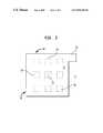
- FIG. 3is a plan view of a bond pad according to the present invention.
- FIGS. 4A-4Jare cross-sectional views of the various sequences of process operations used to form exemplary embodiments of the present invention.
- FIG. 1is a cross-sectional view showing the bond pad structure of the present invention.
- Bond pad 27is formed within bond pad region 40 formed over substrate 1 .
- active devicessuch as transistor 7 may be formed within bond pad region 40 and beneath bond pad 27 .
- FIG. 1shows bond pad 27 formed within bond pad region 40 over substrate 1 .
- Substrate 1may be any suitable substrate on which semiconductor devices and integrated circuits are formed.
- substrate 1may be a silicon wafer.
- Bond pad 27is formed of metal film 17 .
- Metal film 17may be any suitable metal film used as a conductive film within an integrated circuit. Examples of such conductive films include tungsten, aluminum, copper and their alloys such as AlCuSi. In other exemplary embodiments (not shown), metal film 17 may be a composite film including one of the metal films described above, and another film such as a barrier layer film.
- Bond pad 27includes lower surface 14 which is formed of a barrier layer film 13 .
- barrier layer film 13also extends peripherally beyond bond pad region 40 .
- Top surface 24 of bond pad 27is essentially coplanar with top surface 23 of upper dielectric film 15 , within which bond pad opening 20 is formed.
- Beneath barrier layer 13is lower dielectric film 11 which generally insulates bond pad 27 from conductive film 5 and other active devices which may be formed beneath the bond pad 27 and within bond pad region 40 .
- via holes 19hereinafter, “vias” provide direct electrical connection between bond pad 27 and conductive film 5 .
- conductive film 5may be a metal film such as aluminum or copper which may be patterned, a polysilicon or other semiconductor film, or a patterned semiconductor film.
- conductive film 5may be a patterned metal alloy film such as AlCuSi or another aluminum or copper alloy.
- Metal film 17is included within opening 20 formed within upper dielectric film 15 . Electrical connection is provided between bond pad 27 and conductive film 5 through vias 19 formed through barrier layer film 13 which forms the bottom surface 14 of the bond pad, and through lower dielectric film 11 . Together, opening 20 and vias 19 form a dual damascene structure.
- conductive film 5is further coupled, by means of contact 9 formed in insulating film 3 , to transistor 7 formed on substrate 1 within bond pad region 40 . In other exemplary embodiments, conductive film 5 may be additionally or alternatively connected laterally to other devices not included within bond pad region 40 .
- FIG. 1shows vias 19 each directly extending to surface 6 of conductive film 5 , it should be understood that, in embodiments where the conductive film is a patterned film, vias 19 may additionally or alternatively extend down to areas within bond pad region 40 where patterned conductive film 5 is not present.
- Insulating film 3generally insulates conductive film 5 from other devices formed on and within substrate 1 within bond pad region 40 .
- transistor 7is shown including source region S and drain region D formed within substrate 1 beneath bond pad 27 and within bond pad region 40 , other active devices may be used. It is an advantage of the present invention that any of various active devices may be formed in or on substrate 1 within bond pad region 40 and beneath bond pad 27 because of the dual damascene structure of the bond pad and the presence of barrier layer film 13 forming the lower surface of the bond pad opening within bond pad region 40 . It should be further understood that more than one active device may be included within the bond pad region 40 .
- the completed structure shown in FIG. 1also includes conductive external wire 25 bonded to top surface 24 of bond pad 27 . Because of the structure of the bond pad of the present invention, when external wire 25 is bonded to top surface 24 using conventional bonding methods which typically stress the underlying substrate, cracks are prevented from forming in underlying dielectric films such as lower dielectric film 11 . As such, the effects of the stress associated with the bonding process, are reduced. Leakage through the underlying dielectric film is suppressed, allowing for active devices such as transistor 7 to be included beneath bond pad 27 within bond pad region 40 .
- FIG. 2shows another exemplary embodiment of the bond pad structure according to the present invention.
- the structure shown in FIG. 2is substantially the same as the bond pad structure shown in FIG. 1 , with the exception being that, in FIG. 2 , barrier layer film 13 does not extend peripherally beyond bond pad region 40 .
- the presence of barrier layer film 13 within bond pad region 40 and the dual damascene structure of bond pad 27 including vias 19suffices to suppress stress related defects in the underlying films during the bonding process by which external conductive wire 25 is bonded to top surface 24 of bond pad 27 .
- Other features of FIG. 2are identical to the features in FIG. 1 and are as described in conjunction with FIG. 1 .
- FIG. 3is a plan view which represents a top view of each of the cross-sectional structures shown in FIGS. 1 and 2 .
- dashed lines 19represent vias shown in FIGS. 1 and 2 which extend down from the bond pad and which may provide connection to features formed beneath the bond pad and within bond pad region 40 .
- Lead line 29provides electrical connection to other features formed on or within substrate 1 .
- the configuration of bond pad 27is not intended to be limited to the square structure shown in FIG. 3 . Rather, bond pad 27 may take on various shapes. For example, the shape of bond pad 27 may be rectangular, trapezoidal, or rounded.
- the bond pad structure of the present inventionis not intended to be limited to the number and arrangement of vias 19 shown in FIG. 3 .
- the nine vias shown in FIG. 3are intended to be exemplary only.
- the dual damascene bond pad structure formed according to the present inventionmay include any number of via openings 19 , including a single via within bond pad region 40 .
- FIGS. 1 , 2 and 3With respect to each of FIGS. 1 , 2 and 3 , it should be stressed that various features have been expanded or reduced for clarity.
- the relative dimensions of the features shown in FIGS. 1-3are not intended to accurately represent the actual relative dimensions of the features in the physical embodiment; rather, they are primarily illustrative.
- the thickness of each of the films shownhas been increased with respect to the lateral dimension of the bond pad structure, in order to illustrate the relative arrangement of the films.
- FIGS. 4A-4Jshow the sequence of process operations used to form various exemplary embodiments of the bond pad structure.
- FIG. 4Ais a cross-sectional view showing conductive film 5 , over which the bond pad structure of the present invention will be formed.
- conductive film 5is formed within the bond pad region and over a substrate which includes active devices formed beneath conductive film 5 within the bond pad region.
- bond pad region 40includes active devices formed on or within the substrate and beneath the bond pad.
- conductive film 5may be a metal film such as tungsten, aluminum, copper, an aluminum alloy, or a copper alloy, or it may be a semiconductor film such as polysilicon or the like.
- Conductive film 5may be a patterned film, and in an exemplary embodiment will be patterned within the region (bond pad region 40 ) above which the bond pad will be formed.
- Lower dielectric film 11may be an oxide, oxynitride, or other insulating film, and may be formed by conventional methods such as chemical vapor deposition (CVD).
- FIG. 4Cshows barrier layer film 13 formed over lower dielectric film 11 .
- Barrier layer film 13may be formed by conventional methods such as CVD, sputtering or evaporation.
- Barrier layer film 13includes top surface 14 which will ultimately form the lower surface of a bond pad opening which will be formed in a subsequently deposited, superjacent dielectric film.
- Barrier layer film 13is shown as formed within bond pad region 40 and also extending laterally beyond bond pad region 40 .
- barrier layer filmmay be patterned using conventional methods and will remain only within bond pad region 40 .
- barrier layer film 13may be a film formed of tantalum (Ta), tantalum silicide (TaSi), tantalum nitride (TaN), titanium (Ti), titanium silicide (TiSi), titanium nitride (TiN), tungsten silicide (WSi), or tungsten silicide nitride (WSiN).
- barrier layer film 13may represent a composite film formed using any of the above barrier layer films in combination. Thickness 21 of barrier layer film 13 may be any suitable thickness as determined by device requirements, but will preferably be within the range of 500 to 2000 angstroms.
- upper dielectric film 15is formed over top surface 14 of barrier layer film 13 .
- Upper dielectric film 15may be an oxide, oxynitride, or other insulating film, and may be the same or a different film than lower dielectric film 11 .
- Thickness 16 of upper dielectric film 15may be any suitable thickness as determined by device requirements. In various exemplary embodiments, thickness 16 may range from 200 to 20,000 angstroms.
- Upper dielectric film 15includes top surface 23 , and may be formed using conventional methods such as CVD or plasma enhanced-CVD.
- FIG. 4Eshows bond pad opening 20 formed within bond pad region 40 by removing the portions of upper dielectric film 15 which are in bond pad region 40 . This is accomplished by forming a masking pattern within a masking film 31 formed over top surface 23 of upper dielectric film 15 . Conventional processing techniques, such as by coating a photosensitive masking film 31 such as photoresist, over top surface 23 , then subsequently patterning the film using conventional methods, may be used. After a pattern is formed in masking film 31 , opening 20 is then formed by etching methods. Wet, chemical etching methods may be used, or dry, RIE (reactive ion etching) plasma etching methods may be employed.
- RIEreactive ion etching
- any suitable etching procedure which selectively removes upper dielectric film 15 from bond pad region 40 , and which does not significantly attack barrier layer film 13may be used.
- the entire thickness 16 of upper dielectric film 15is removed by etching, producing opening 20 which includes lower surface 14 which is also the top surface of barrier layer film 13 .
- at least one active deviceis formed (as shown in FIGS. 1 and 2 ). After opening 20 is formed, masking film 31 may be removed by conventional methods.
- FIG. 4Fshows the subsequent patterning step used in the dual damascene processing sequence.
- masking film 33is formed and patterned using conventional methods.
- masking film 33may be a photosensitive film similar or identical to the photosensitive film 31 shown in FIG. 4E.
- a patternis formed which includes vias 19 which may provide for electrical contact between the metal bond pad to be formed within bond pad opening 20 (as will be shown in FIG. 4H ) and conductive film 5 .
- RIE or plasma etching techniqueswill be used to remove portions of barrier layer film 13 which are not covered by masking film 33 .
- FIG. 4Gshows via openings 19 extending from bond pad opening 20 to exposed surface 6 of underlying conductive film 5 .
- masking film 33may be removed using conventional methods. It should be understood that, in various exemplary embodiments, conductive film 5 may be a patterned film.
- vias 19may extend down to surface 6 of the patterned conductive film 5 , thereby exposing a region of patterned conductive film 5 , or the vias may alternatively extend down to other features within bond pad region 40 , in areas where patterned conductive film 5 is not present. It should be further understood that any number of vias may be formed through the bottom of bond pad opening 20 , according to various exemplary embodiments.
- the via or viasare first formed within the bond pad region. Via openings are formed by patterning a first masking film to produce a pattern similar to that of masking film 33 shown in FIG. 4F , then etching through the entire thickness of the upper dielectric, and barrier layer films. After the first masking film is removed, another pattern is formed using a second masking film and exposing the entire bond pad region, which is then etched to remove the entire thickness of the upper dielectric film from the bond pad region.
- This dielectric etchsimultaneously etches the via openings down to the upper surface of the underlying conductive film, producing the vias and the structure shown in FIG. 4G after the second masking film is removed.
- a different process sequenceis used to according to this exemplary embodiment, the resulting structure as shown in FIG. 4G , is the same.
- FIG. 4Hshows metal film 17 formed within bond pad opening 20 and within vias 19 thereby providing electrical contact from bond pad 27 to underlying features such as conductive film 5 .
- Metal film 17may be a tungsten film, a copper film, an aluminum film, alloys such as an aluminum silicon film or an aluminum copper silicon film, or other suitable metal films.
- Bond pad metal film 17may be formed by sputter deposition, evaporation, chemical vapor deposition or other means. Upon deposition, metal film 17 is a continuous film including portions formed above top surface 23 of upper dielectric film 15 . In one exemplary embodiment, the thickness 18 of metal film 17 is chosen to be greater than the depth of the bond pad opening 20 (thickness 16 of upper dielectric film 15 as shown in FIG.
- Thickness 18 of metal film 17may vary according to the thickness of upper dielectric film 15 , but may be as great as 2 microns.
- polishing methodssuch as chemical mechanical polishing (CMP) may be used to remove portions of metal film 17 which lie above top surface 23 , thereby producing the bond pad structure shown in FIG. 4 I. It can be seen that top surface 23 and upper surface 24 of bond pad 27 , form a smooth continuous surface and are substantially coplanar. Top surface 23 of bond pad 27 may be subsequently bonded to an external conductive wire, as shown in FIG. 1 .
- FIG. 4Jshows another exemplary embodiment of the bond pad of the present invention.
- the bond pad shown in FIG. 4Jincludes upper barrier film 35 .
- Upper barrier film 35is added to the structure in the following manner. Instead of depositing metal film 17 having a thickness sufficient to completely fill bond pad opening 20 (as used to form the structure shown in FIG. 4 H), the deposition of metal film 17 is stopped before metal film 17 completely fills bond pad opening 20 . At this point, upper barrier layer film 35 is formed over the top surface of bond pad metal film 17 , including a portion within bond pad opening 20 .
- Upper barrier layer film 35may include any of the films listed in conjunction with barrier layer film 13 and may have a thickness as great as 1000 angstroms.
- Upper barrier layer film 35may be formed using sputtering techniques, or chemical vapor deposition or other deposition processes. After upper barrier layer film 35 is formed over bond pad metal film 17 and within bond pad region 20 , a polishing technique such as CMP is used to remove portions of both bond pad metal film 17 and upper barrier film 35 which lie above top surface 23 of upper dielectric film 15 .
- CMPpolishing technique
- the bond pad of the exemplary embodiment shown in FIG. 4Jwill also include active devices formed beneath the bond pad. This feature is shown in the completed bond pad structures shown in the exemplary embodiments of FIGS. 1 and 2 . Furthermore, this exemplary embodiment may alternatively include barrier layer film 13 being removed from regions outside bond pad region 40 . It should be further understood that the exemplary embodiment shown in FIG. 4J , may also be bonded to an external conductive wire as shown in each of FIGS. 1 and 2 .
- the process and structureencompass a plurality of bond pads formed simultaneously within a plurality of integrated circuit devices formed on a substrate.
- the inventionis not intended to be limited to a particular structure beneath the bond pads; rather, the present invention covers bond pads formed within a bond pad opening having a barrier layer film as a bottom surface, with any number of vias extending vertically beneath the bottom surface within the bond pad region.
- Beneath the bond padmay be a conductive film which may be patterned, and any number of different active devices within the bond pad area.
- the viasmay provide electrical connection to the conductive film or other subjacent active devices.
- the conductive film beneath the bond padmay be coupled to active devices within or external to the bond pad region.
- the individual bond pads which combine to form an individual integrated circuit devicemay also vary from one another in structure.
Landscapes
- Engineering & Computer Science (AREA)
- Computer Hardware Design (AREA)
- Microelectronics & Electronic Packaging (AREA)
- Power Engineering (AREA)
- Physics & Mathematics (AREA)
- Condensed Matter Physics & Semiconductors (AREA)
- General Physics & Mathematics (AREA)
- Manufacturing & Machinery (AREA)
- Internal Circuitry In Semiconductor Integrated Circuit Devices (AREA)
Abstract
Description
Claims (23)
Priority Applications (5)
| Application Number | Priority Date | Filing Date | Title |
|---|---|---|---|
| US09/465,089US6838769B1 (en) | 1999-12-16 | 1999-12-16 | Dual damascene bond pad structure for lowering stress and allowing circuitry under pads |
| GB0030319AGB2364170B (en) | 1999-12-16 | 2000-12-12 | Dual damascene bond pad structure for lowering stress and allowing circuitry under pads and a process to form the same |
| JP2000381501AJP4138232B2 (en) | 1999-12-16 | 2000-12-15 | Dual etched bond pad structure for reducing stress and allowing circuitry to be placed under the pad and method for forming the same |
| KR1020000076794AKR100691051B1 (en) | 1999-12-16 | 2000-12-15 | Semiconductor Device and Bond Pad Formation Process |
| TW089126837ATW477000B (en) | 1999-12-16 | 2001-01-03 | Dual damascene bond pad structure for lowering stress and allowing circuitry under pads and a process to form same |
Applications Claiming Priority (1)
| Application Number | Priority Date | Filing Date | Title |
|---|---|---|---|
| US09/465,089US6838769B1 (en) | 1999-12-16 | 1999-12-16 | Dual damascene bond pad structure for lowering stress and allowing circuitry under pads |
Publications (1)
| Publication Number | Publication Date |
|---|---|
| US6838769B1true US6838769B1 (en) | 2005-01-04 |
Family
ID=33539010
Family Applications (1)
| Application Number | Title | Priority Date | Filing Date |
|---|---|---|---|
| US09/465,089Expired - LifetimeUS6838769B1 (en) | 1999-12-16 | 1999-12-16 | Dual damascene bond pad structure for lowering stress and allowing circuitry under pads |
Country Status (1)
| Country | Link |
|---|---|
| US (1) | US6838769B1 (en) |
Cited By (10)
| Publication number | Priority date | Publication date | Assignee | Title |
|---|---|---|---|---|
| US20040150112A1 (en)* | 2003-01-30 | 2004-08-05 | Nec Electronics Corporation | Semiconductor device and method of fabrication same |
| US20040201102A1 (en)* | 2003-04-09 | 2004-10-14 | Sharp Kabushiki Kaisha | Semiconductor device |
| US20070262460A1 (en)* | 1998-12-21 | 2007-11-15 | Mou-Shiung Lin | Top layers of metal for high performance IC's |
| US20080105947A1 (en)* | 2006-10-24 | 2008-05-08 | Denso Corporation | Semiconductor device, wiring of semiconductor device, and method of forming wiring |
| US7405149B1 (en)* | 1998-12-21 | 2008-07-29 | Megica Corporation | Post passivation method for semiconductor chip or wafer |
| US7741716B1 (en) | 2005-11-08 | 2010-06-22 | Altera Corporation | Integrated circuit bond pad structures |
| US8304907B2 (en) | 1998-12-21 | 2012-11-06 | Megica Corporation | Top layers of metal for integrated circuits |
| US20130048982A1 (en)* | 2011-08-31 | 2013-02-28 | Stmicroelectronics S.R.I. | Bond pad monitoring structure and related method of detecting significant alterations |
| US20170110429A1 (en)* | 2015-10-19 | 2017-04-20 | Taiwan Semiconductor Manufacturing Company Ltd. | Semiconductor device with an anti-pad peeling structure and associated method |
| CN113539945A (en)* | 2020-04-16 | 2021-10-22 | 长鑫存储技术有限公司 | Semiconductor structure and forming method thereof |
Citations (15)
| Publication number | Priority date | Publication date | Assignee | Title |
|---|---|---|---|---|
| EP0224013A2 (en) | 1985-10-28 | 1987-06-03 | International Business Machines Corporation | Method for producing coplanar multi-level metal/insulator films on a substrate |
| US5229645A (en) | 1990-06-21 | 1993-07-20 | Mitsubishi Denki Kabushiki Kaisha | Semiconductor device and manufacturing method thereof |
| US5451551A (en) | 1993-06-09 | 1995-09-19 | Krishnan; Ajay | Multilevel metallization process using polishing |
| US5741626A (en) | 1996-04-15 | 1998-04-21 | Motorola, Inc. | Method for forming a dielectric tantalum nitride layer as an anti-reflective coating (ARC) |
| US5751065A (en)* | 1993-08-05 | 1998-05-12 | Lucent Technologies Inc. | Integrated circuit with active devices under bond pads |
| US5824599A (en)* | 1996-01-16 | 1998-10-20 | Cornell Research Foundation, Inc. | Protected encapsulation of catalytic layer for electroless copper interconnect |
| US5932487A (en) | 1998-03-12 | 1999-08-03 | Worldwide Semiconductor Manufacturing Corporation | Method for forming a planar intermetal dielectric layer |
| US6033984A (en) | 1997-12-23 | 2000-03-07 | Siemens Aktiengesellschaft | Dual damascene with bond pads |
| US6054383A (en) | 1995-11-21 | 2000-04-25 | Nec Corporation | Fabrication method of semiconductor device |
| US6093630A (en) | 1996-07-25 | 2000-07-25 | International Business Machines Corporation | Semi-conductor personalization structure and method |
| US6103616A (en) | 1998-08-19 | 2000-08-15 | Advanced Micro Devices, Inc. | Method to manufacture dual damascene structures by utilizing short resist spacers |
| US6144099A (en) | 1999-03-30 | 2000-11-07 | Advanced Micro Devices, Inc. | Semiconductor metalization barrier |
| US6143646A (en) | 1997-06-03 | 2000-11-07 | Motorola Inc. | Dual in-laid integrated circuit structure with selectively positioned low-K dielectric isolation and method of formation |
| US6180506B1 (en) | 1998-09-14 | 2001-01-30 | International Business Machines Corporation | Upper redundant layer for damascene metallization |
| US6239494B1 (en)* | 1999-04-21 | 2001-05-29 | Advanced Micro Devices, Inc. | Wire bonding CU interconnects |
- 1999
- 1999-12-16USUS09/465,089patent/US6838769B1/ennot_activeExpired - Lifetime
Patent Citations (15)
| Publication number | Priority date | Publication date | Assignee | Title |
|---|---|---|---|---|
| EP0224013A2 (en) | 1985-10-28 | 1987-06-03 | International Business Machines Corporation | Method for producing coplanar multi-level metal/insulator films on a substrate |
| US5229645A (en) | 1990-06-21 | 1993-07-20 | Mitsubishi Denki Kabushiki Kaisha | Semiconductor device and manufacturing method thereof |
| US5451551A (en) | 1993-06-09 | 1995-09-19 | Krishnan; Ajay | Multilevel metallization process using polishing |
| US5751065A (en)* | 1993-08-05 | 1998-05-12 | Lucent Technologies Inc. | Integrated circuit with active devices under bond pads |
| US6054383A (en) | 1995-11-21 | 2000-04-25 | Nec Corporation | Fabrication method of semiconductor device |
| US5824599A (en)* | 1996-01-16 | 1998-10-20 | Cornell Research Foundation, Inc. | Protected encapsulation of catalytic layer for electroless copper interconnect |
| US5741626A (en) | 1996-04-15 | 1998-04-21 | Motorola, Inc. | Method for forming a dielectric tantalum nitride layer as an anti-reflective coating (ARC) |
| US6093630A (en) | 1996-07-25 | 2000-07-25 | International Business Machines Corporation | Semi-conductor personalization structure and method |
| US6143646A (en) | 1997-06-03 | 2000-11-07 | Motorola Inc. | Dual in-laid integrated circuit structure with selectively positioned low-K dielectric isolation and method of formation |
| US6033984A (en) | 1997-12-23 | 2000-03-07 | Siemens Aktiengesellschaft | Dual damascene with bond pads |
| US5932487A (en) | 1998-03-12 | 1999-08-03 | Worldwide Semiconductor Manufacturing Corporation | Method for forming a planar intermetal dielectric layer |
| US6103616A (en) | 1998-08-19 | 2000-08-15 | Advanced Micro Devices, Inc. | Method to manufacture dual damascene structures by utilizing short resist spacers |
| US6180506B1 (en) | 1998-09-14 | 2001-01-30 | International Business Machines Corporation | Upper redundant layer for damascene metallization |
| US6144099A (en) | 1999-03-30 | 2000-11-07 | Advanced Micro Devices, Inc. | Semiconductor metalization barrier |
| US6239494B1 (en)* | 1999-04-21 | 2001-05-29 | Advanced Micro Devices, Inc. | Wire bonding CU interconnects |
Cited By (51)
| Publication number | Priority date | Publication date | Assignee | Title |
|---|---|---|---|---|
| US7456100B2 (en) | 1998-12-21 | 2008-11-25 | Mou-Shiung Lin | Top layers of metal for high performance IC's |
| US8471384B2 (en) | 1998-12-21 | 2013-06-25 | Megica Corporation | Top layers of metal for high performance IC's |
| US20070262458A1 (en)* | 1998-12-21 | 2007-11-15 | Mou-Shiung Lin | Top layers of metal for high performance IC's |
| US20070278688A1 (en)* | 1998-12-21 | 2007-12-06 | Mou-Shiung Lin | Top layers of metal for high performance IC's |
| US20070288880A1 (en)* | 1998-12-21 | 2007-12-13 | Mou-Shiung Lin | Top layers of metal for high performance IC's |
| US20070290349A1 (en)* | 1998-12-21 | 2007-12-20 | Mou-Shiung Lin | Top layers of metal for high performance IC's |
| US20070290351A1 (en)* | 1998-12-21 | 2007-12-20 | Mou-Shiung Lin | Top layers of metal for high performance IC's |
| US20070290350A1 (en)* | 1998-12-21 | 2007-12-20 | Mou-Shiung Lin | Top layers of metal for high performance IC's |
| US20070290358A1 (en)* | 1998-12-21 | 2007-12-20 | Mou-Shiung Lin | Top layers of metal for high performance IC's |
| US20080083988A1 (en)* | 1998-12-21 | 2008-04-10 | Mou-Shiung Lin | Top layers of metal for high performance IC's |
| US7358610B2 (en) | 1998-12-21 | 2008-04-15 | Mou-Shiung Lin | Top layers of metal for high performance IC's |
| US7382058B2 (en) | 1998-12-21 | 2008-06-03 | Mou-Shiung Lin | Top layers of metal for high performance IC's |
| US7385292B2 (en) | 1998-12-21 | 2008-06-10 | Mou-Shiung Lin | Top layers of metal for high performance IC's |
| US7385291B2 (en) | 1998-12-21 | 2008-06-10 | Mou-Shiung Lin | Top layers of metal for high performance IC's |
| US8531038B2 (en) | 1998-12-21 | 2013-09-10 | Megica Corporation | Top layers of metal for high performance IC's |
| US8415800B2 (en) | 1998-12-21 | 2013-04-09 | Megica Corporation | Top layers of metal for high performance IC's |
| US7388292B2 (en) | 1998-12-21 | 2008-06-17 | Mou-Shiung Lin | Top layers of metal for high performance IC's |
| US7396756B2 (en) | 1998-12-21 | 2008-07-08 | Mou-Shiung Lin | Top layers of metal for high performance IC's |
| US7397135B2 (en) | 1998-12-21 | 2008-07-08 | Mou-Shiung Lin | Top layers of metal for high performance IC's |
| US8350386B2 (en) | 1998-12-21 | 2013-01-08 | Megica Corporation | Top layers of metal for high performance IC's |
| US7405149B1 (en)* | 1998-12-21 | 2008-07-29 | Megica Corporation | Post passivation method for semiconductor chip or wafer |
| US7425764B2 (en) | 1998-12-21 | 2008-09-16 | Mou-Shiung Lin | Top layers of metal for high performance IC's |
| US20080246154A1 (en)* | 1998-12-21 | 2008-10-09 | Megica Corporation | Top layers of metal for high performance IC's |
| US7442969B2 (en) | 1998-12-21 | 2008-10-28 | Mou-Shiung Lin | Top layers of metal for high performance IC's |
| US20070262459A1 (en)* | 1998-12-21 | 2007-11-15 | Mou-Shiung Lin | Top layers of metal for high performance IC's |
| US20070262460A1 (en)* | 1998-12-21 | 2007-11-15 | Mou-Shiung Lin | Top layers of metal for high performance IC's |
| US7863654B2 (en) | 1998-12-21 | 2011-01-04 | Megica Corporation | Top layers of metal for high performance IC's |
| US7482693B2 (en) | 1998-12-21 | 2009-01-27 | Mou-Shiung Lin | Top layers of metal for high performance IC's |
| US8304907B2 (en) | 1998-12-21 | 2012-11-06 | Megica Corporation | Top layers of metal for integrated circuits |
| US8022545B2 (en) | 1998-12-21 | 2011-09-20 | Megica Corporation | Top layers of metal for high performance IC's |
| US8022546B2 (en) | 1998-12-21 | 2011-09-20 | Megica Corporation | Top layers of metal for high performance IC's |
| US7999384B2 (en) | 1998-12-21 | 2011-08-16 | Megica Corporation | Top layers of metal for high performance IC's |
| US7884479B2 (en) | 1998-12-21 | 2011-02-08 | Megica Corporation | Top layers of metal for high performance IC's |
| US20100117236A1 (en)* | 1998-12-21 | 2010-05-13 | Megica Corporation | Top layers of metal for high performance ic's |
| US7465975B2 (en) | 1998-12-21 | 2008-12-16 | Mou-Shiung Lin | Top layers of metal for high performance IC's |
| US7397125B2 (en)* | 2003-01-30 | 2008-07-08 | Nec Electronics Corporation | Semiconductor device with bonding pad support structure |
| US7714449B2 (en) | 2003-01-30 | 2010-05-11 | Nec Electronics Corporation | Semiconductor device with bonding pad support structure |
| US20040150112A1 (en)* | 2003-01-30 | 2004-08-05 | Nec Electronics Corporation | Semiconductor device and method of fabrication same |
| US20080088023A1 (en)* | 2003-01-30 | 2008-04-17 | Nec Electronics Corporation | Semiconductor device with bonding pad support structure |
| US20080290516A1 (en)* | 2003-01-30 | 2008-11-27 | Nec Electronics Corporation | Semiconductor device with bonding pad support structure |
| US7385289B2 (en)* | 2003-04-09 | 2008-06-10 | Sharp Kabushiki Kaisha | Semiconductor device using inorganic film between wiring layer and bonding pad |
| US20040201102A1 (en)* | 2003-04-09 | 2004-10-14 | Sharp Kabushiki Kaisha | Semiconductor device |
| US7741716B1 (en) | 2005-11-08 | 2010-06-22 | Altera Corporation | Integrated circuit bond pad structures |
| US20080105947A1 (en)* | 2006-10-24 | 2008-05-08 | Denso Corporation | Semiconductor device, wiring of semiconductor device, and method of forming wiring |
| US7642653B2 (en) | 2006-10-24 | 2010-01-05 | Denso Corporation | Semiconductor device, wiring of semiconductor device, and method of forming wiring |
| US20130048982A1 (en)* | 2011-08-31 | 2013-02-28 | Stmicroelectronics S.R.I. | Bond pad monitoring structure and related method of detecting significant alterations |
| US8803145B2 (en)* | 2011-08-31 | 2014-08-12 | Stmicroelectronics S.R.L. | Bond pad monitoring structure and related method of detecting significant alterations |
| US20170110429A1 (en)* | 2015-10-19 | 2017-04-20 | Taiwan Semiconductor Manufacturing Company Ltd. | Semiconductor device with an anti-pad peeling structure and associated method |
| US9711478B2 (en)* | 2015-10-19 | 2017-07-18 | Taiwan Semiconductor Manufacturing Company Ltd. | Semiconductor device with an anti-pad peeling structure and associated method |
| CN113539945A (en)* | 2020-04-16 | 2021-10-22 | 长鑫存储技术有限公司 | Semiconductor structure and forming method thereof |
| CN113539945B (en)* | 2020-04-16 | 2023-09-29 | 长鑫存储技术有限公司 | Semiconductor structure and forming method thereof |
Similar Documents
| Publication | Publication Date | Title |
|---|---|---|
| US6417087B1 (en) | Process for forming a dual damascene bond pad structure over active circuitry | |
| JP3526376B2 (en) | Semiconductor device and manufacturing method thereof | |
| US5707894A (en) | Bonding pad structure and method thereof | |
| US6803302B2 (en) | Method for forming a semiconductor device having a mechanically robust pad interface | |
| US7211902B2 (en) | Method of forming a bonding pad structure | |
| US8901733B2 (en) | Reliable metal bumps on top of I/O pads after removal of test probe marks | |
| US6656826B2 (en) | Semiconductor device with fuse to be blown with energy beam and method of manufacturing the semiconductor device | |
| US6333559B1 (en) | Method/structure for creating aluminum wirebound pad on copper BEOL | |
| JP4037561B2 (en) | Manufacturing method of semiconductor device | |
| KR100411576B1 (en) | Copper pad structure | |
| US20080164574A1 (en) | Integrated circuits with conductive features in through holes passing through other conductive features and through a semiconductor substrate | |
| JP4138232B2 (en) | Dual etched bond pad structure for reducing stress and allowing circuitry to be placed under the pad and method for forming the same | |
| US6576970B2 (en) | Bonding pad structure of semiconductor device and method for fabricating the same | |
| US6838769B1 (en) | Dual damascene bond pad structure for lowering stress and allowing circuitry under pads | |
| JP5258142B2 (en) | Aluminum pad power bus and signal routing technology for integrated circuit devices using copper technology interconnect structures | |
| EP0926721A2 (en) | Dual damascene with bond pads | |
| US20020068385A1 (en) | Method for forming anchored bond pads in semiconductor devices and devices formed | |
| JP2001326242A (en) | Semiconductor device and method of manufacturing the same | |
| KR20040056957A (en) | Method for forming a pad of a semiconductor device | |
| JPS60187039A (en) | Multilayer wiring components | |
| JP2000216250A (en) | Semiconductor device and manufacture of it | |
| HK1018354A (en) | Dual damascene with bond pade | |
| JP2004047859A (en) | Semiconductor device | |
| KR20020060452A (en) | Semiconductor integrated circuit and method for manufacturing the same |
Legal Events
| Date | Code | Title | Description |
|---|---|---|---|
| AS | Assignment | Owner name:LUCENT TECHNOLOGIES, INC., NEW JERSEY Free format text:ASSIGNMENT OF ASSIGNORS INTEREST;ASSIGNORS:CHITTIPEDDI, SAILESH;COCHRAN, WILLIAM THOMAS;SMOOHA, YEHUDA;REEL/FRAME:010471/0915;SIGNING DATES FROM 19991015 TO 19991210 | |
| FEPP | Fee payment procedure | Free format text:PAYOR NUMBER ASSIGNED (ORIGINAL EVENT CODE: ASPN); ENTITY STATUS OF PATENT OWNER: LARGE ENTITY Free format text:PAYER NUMBER DE-ASSIGNED (ORIGINAL EVENT CODE: RMPN); ENTITY STATUS OF PATENT OWNER: LARGE ENTITY | |
| STCF | Information on status: patent grant | Free format text:PATENTED CASE | |
| FPAY | Fee payment | Year of fee payment:4 | |
| FPAY | Fee payment | Year of fee payment:8 | |
| AS | Assignment | Owner name:DEUTSCHE BANK AG NEW YORK BRANCH, AS COLLATERAL AG Free format text:PATENT SECURITY AGREEMENT;ASSIGNORS:LSI CORPORATION;AGERE SYSTEMS LLC;REEL/FRAME:032856/0031 Effective date:20140506 | |
| AS | Assignment | Owner name:AVAGO TECHNOLOGIES GENERAL IP (SINGAPORE) PTE. LTD Free format text:ASSIGNMENT OF ASSIGNORS INTEREST;ASSIGNOR:AGERE SYSTEMS LLC;REEL/FRAME:035059/0001 Effective date:20140804 Owner name:AGERE SYSTEMS LLC, PENNSYLVANIA Free format text:MERGER;ASSIGNOR:AGERE SYSTEMS INC.;REEL/FRAME:035058/0895 Effective date:20120724 Owner name:AGERE SYSTEMS GUARDIAN CORP., PENNSYLVANIA Free format text:ASSIGNMENT OF ASSIGNORS INTEREST;ASSIGNOR:LUCENT TECHNOLOGIES INC.;REEL/FRAME:035058/0646 Effective date:20010130 Owner name:AGERE SYSTEMS INC., PENNSYLVANIA Free format text:MERGER;ASSIGNOR:AGERE SYSTEMS GUARDIAN CORP.;REEL/FRAME:035058/0884 Effective date:20020822 | |
| AS | Assignment | Owner name:LSI CORPORATION, CALIFORNIA Free format text:TERMINATION AND RELEASE OF SECURITY INTEREST IN PATENT RIGHTS (RELEASES RF 032856-0031);ASSIGNOR:DEUTSCHE BANK AG NEW YORK BRANCH, AS COLLATERAL AGENT;REEL/FRAME:037684/0039 Effective date:20160201 Owner name:AGERE SYSTEMS LLC, PENNSYLVANIA Free format text:TERMINATION AND RELEASE OF SECURITY INTEREST IN PATENT RIGHTS (RELEASES RF 032856-0031);ASSIGNOR:DEUTSCHE BANK AG NEW YORK BRANCH, AS COLLATERAL AGENT;REEL/FRAME:037684/0039 Effective date:20160201 | |
| AS | Assignment | Owner name:BANK OF AMERICA, N.A., AS COLLATERAL AGENT, NORTH CAROLINA Free format text:PATENT SECURITY AGREEMENT;ASSIGNOR:AVAGO TECHNOLOGIES GENERAL IP (SINGAPORE) PTE. LTD.;REEL/FRAME:037808/0001 Effective date:20160201 Owner name:BANK OF AMERICA, N.A., AS COLLATERAL AGENT, NORTH Free format text:PATENT SECURITY AGREEMENT;ASSIGNOR:AVAGO TECHNOLOGIES GENERAL IP (SINGAPORE) PTE. LTD.;REEL/FRAME:037808/0001 Effective date:20160201 | |
| FPAY | Fee payment | Year of fee payment:12 | |
| AS | Assignment | Owner name:AVAGO TECHNOLOGIES GENERAL IP (SINGAPORE) PTE. LTD., SINGAPORE Free format text:TERMINATION AND RELEASE OF SECURITY INTEREST IN PATENTS;ASSIGNOR:BANK OF AMERICA, N.A., AS COLLATERAL AGENT;REEL/FRAME:041710/0001 Effective date:20170119 Owner name:AVAGO TECHNOLOGIES GENERAL IP (SINGAPORE) PTE. LTD Free format text:TERMINATION AND RELEASE OF SECURITY INTEREST IN PATENTS;ASSIGNOR:BANK OF AMERICA, N.A., AS COLLATERAL AGENT;REEL/FRAME:041710/0001 Effective date:20170119 | |
| AS | Assignment | Owner name:CORTLAND CAPITAL MARKET SERVICES LLC, AS COLLATERA Free format text:SECURITY INTEREST;ASSIGNORS:HILCO PATENT ACQUISITION 56, LLC;BELL SEMICONDUCTOR, LLC;BELL NORTHERN RESEARCH, LLC;REEL/FRAME:045216/0020 Effective date:20180124 | |
| AS | Assignment | Owner name:BELL SEMICONDUCTOR, LLC, ILLINOIS Free format text:ASSIGNMENT OF ASSIGNORS INTEREST;ASSIGNORS:AVAGO TECHNOLOGIES GENERAL IP (SINGAPORE) PTE. LTD.;BROADCOM CORPORATION;REEL/FRAME:050635/0001 Effective date:20171208 |