US6838723B2 - Merged MOS-bipolar capacitor memory cell - Google Patents
Merged MOS-bipolar capacitor memory cellDownload PDFInfo
- Publication number
- US6838723B2 US6838723B2US10/230,929US23092902AUS6838723B2US 6838723 B2US6838723 B2US 6838723B2US 23092902 AUS23092902 AUS 23092902AUS 6838723 B2US6838723 B2US 6838723B2
- Authority
- US
- United States
- Prior art keywords
- region
- vertical
- transistor
- mos transistor
- cell
- Prior art date
- Legal status (The legal status is an assumption and is not a legal conclusion. Google has not performed a legal analysis and makes no representation as to the accuracy of the status listed.)
- Expired - Lifetime
Links
- 239000003990capacitorSubstances0.000titleclaimsabstractdescription64
- 230000015654memoryEffects0.000titleclaimsdescription99
- 238000007667floatingMethods0.000claimsabstractdescription54
- 210000000746body regionAnatomy0.000claimsabstractdescription40
- 238000003860storageMethods0.000claimsdescription20
- 239000000758substrateSubstances0.000claimsdescription17
- 239000004065semiconductorSubstances0.000claimsdescription12
- 230000006870functionEffects0.000claimsdescription6
- 239000000463materialSubstances0.000description12
- 238000004519manufacturing processMethods0.000description8
- 235000012431wafersNutrition0.000description8
- 238000000034methodMethods0.000description6
- XUIMIQQOPSSXEZ-UHFFFAOYSA-NSiliconChemical compound[Si]XUIMIQQOPSSXEZ-UHFFFAOYSA-N0.000description5
- 229910052710siliconInorganic materials0.000description5
- 239000010703siliconSubstances0.000description5
- 238000012546transferMethods0.000description5
- 230000003321amplificationEffects0.000description4
- 238000010586diagramMethods0.000description4
- 238000003199nucleic acid amplification methodMethods0.000description4
- 230000015556catabolic processEffects0.000description3
- 230000000295complement effectEffects0.000description3
- 238000005516engineering processMethods0.000description3
- 230000005669field effectEffects0.000description3
- 239000012212insulatorSubstances0.000description3
- 230000009467reductionEffects0.000description3
- 230000008859changeEffects0.000description2
- 238000004891communicationMethods0.000description2
- 238000013461designMethods0.000description2
- 230000009977dual effectEffects0.000description2
- 230000000694effectsEffects0.000description2
- 238000002955isolationMethods0.000description2
- 229910021420polycrystalline siliconInorganic materials0.000description2
- 229920005591polysiliconPolymers0.000description2
- 238000012545processingMethods0.000description2
- -1600-1Chemical compound0.000description1
- 229910052581Si3N4Inorganic materials0.000description1
- 230000009471actionEffects0.000description1
- 230000003213activating effectEffects0.000description1
- LBDSXVIYZYSRII-IGMARMGPSA-Nalpha-particleChemical compound[4He+2]LBDSXVIYZYSRII-IGMARMGPSA-N0.000description1
- 238000013459approachMethods0.000description1
- 238000007796conventional methodMethods0.000description1
- 230000008878couplingEffects0.000description1
- 238000010168coupling processMethods0.000description1
- 238000005859coupling reactionMethods0.000description1
- 238000013500data storageMethods0.000description1
- 230000007423decreaseEffects0.000description1
- 230000003247decreasing effectEffects0.000description1
- 238000006731degradation reactionMethods0.000description1
- 230000008021depositionEffects0.000description1
- 238000001514detection methodMethods0.000description1
- 238000011161developmentMethods0.000description1
- 230000036039immunityEffects0.000description1
- 239000011810insulating materialSubstances0.000description1
- 230000000670limiting effectEffects0.000description1
- 230000000873masking effectEffects0.000description1
- 238000005272metallurgyMethods0.000description1
- 150000004767nitridesChemical class0.000description1
- 230000003647oxidationEffects0.000description1
- 238000007254oxidation reactionMethods0.000description1
- 230000003071parasitic effectEffects0.000description1
- 239000002245particleSubstances0.000description1
- 230000002093peripheral effectEffects0.000description1
- 230000008569processEffects0.000description1
- 238000004886process controlMethods0.000description1
- 230000005855radiationEffects0.000description1
- 230000002441reversible effectEffects0.000description1
- 238000000926separation methodMethods0.000description1
- HQVNEWCFYHHQES-UHFFFAOYSA-Nsilicon nitrideChemical compoundN12[Si]34N5[Si]62N3[Si]51N64HQVNEWCFYHHQES-UHFFFAOYSA-N0.000description1
- 239000007787solidSubstances0.000description1
- 230000003068static effectEffects0.000description1
Images


Classifications
- G—PHYSICS
- G11—INFORMATION STORAGE
- G11C—STATIC STORES
- G11C11/00—Digital stores characterised by the use of particular electric or magnetic storage elements; Storage elements therefor
- G11C11/21—Digital stores characterised by the use of particular electric or magnetic storage elements; Storage elements therefor using electric elements
- G11C11/34—Digital stores characterised by the use of particular electric or magnetic storage elements; Storage elements therefor using electric elements using semiconductor devices
- G11C11/40—Digital stores characterised by the use of particular electric or magnetic storage elements; Storage elements therefor using electric elements using semiconductor devices using transistors
- G11C11/401—Digital stores characterised by the use of particular electric or magnetic storage elements; Storage elements therefor using electric elements using semiconductor devices using transistors forming cells needing refreshing or charge regeneration, i.e. dynamic cells
- G11C11/403—Digital stores characterised by the use of particular electric or magnetic storage elements; Storage elements therefor using electric elements using semiconductor devices using transistors forming cells needing refreshing or charge regeneration, i.e. dynamic cells with charge regeneration common to a multiplicity of memory cells, i.e. external refresh
- G11C11/405—Digital stores characterised by the use of particular electric or magnetic storage elements; Storage elements therefor using electric elements using semiconductor devices using transistors forming cells needing refreshing or charge regeneration, i.e. dynamic cells with charge regeneration common to a multiplicity of memory cells, i.e. external refresh with three charge-transfer gates, e.g. MOS transistors, per cell
- H—ELECTRICITY
- H10—SEMICONDUCTOR DEVICES; ELECTRIC SOLID-STATE DEVICES NOT OTHERWISE PROVIDED FOR
- H10B—ELECTRONIC MEMORY DEVICES
- H10B12/00—Dynamic random access memory [DRAM] devices
- H—ELECTRICITY
- H10—SEMICONDUCTOR DEVICES; ELECTRIC SOLID-STATE DEVICES NOT OTHERWISE PROVIDED FOR
- H10B—ELECTRONIC MEMORY DEVICES
- H10B12/00—Dynamic random access memory [DRAM] devices
- H10B12/20—DRAM devices comprising floating-body transistors, e.g. floating-body cells
- H—ELECTRICITY
- H10—SEMICONDUCTOR DEVICES; ELECTRIC SOLID-STATE DEVICES NOT OTHERWISE PROVIDED FOR
- H10D—INORGANIC ELECTRIC SEMICONDUCTOR DEVICES
- H10D30/00—Field-effect transistors [FET]
- H10D30/60—Insulated-gate field-effect transistors [IGFET]
- H10D30/711—Insulated-gate field-effect transistors [IGFET] having floating bodies
- H—ELECTRICITY
- H10—SEMICONDUCTOR DEVICES; ELECTRIC SOLID-STATE DEVICES NOT OTHERWISE PROVIDED FOR
- H10D—INORGANIC ELECTRIC SEMICONDUCTOR DEVICES
- H10D84/00—Integrated devices formed in or on semiconductor substrates that comprise only semiconducting layers, e.g. on Si wafers or on GaAs-on-Si wafers
- H10D84/40—Integrated devices formed in or on semiconductor substrates that comprise only semiconducting layers, e.g. on Si wafers or on GaAs-on-Si wafers characterised by the integration of at least one component covered by groups H10D12/00 or H10D30/00 with at least one component covered by groups H10D10/00 or H10D18/00, e.g. integration of IGFETs with BJTs
- H10D84/401—Combinations of FETs or IGBTs with BJTs
- H—ELECTRICITY
- H10—SEMICONDUCTOR DEVICES; ELECTRIC SOLID-STATE DEVICES NOT OTHERWISE PROVIDED FOR
- H10B—ELECTRONIC MEMORY DEVICES
- H10B12/00—Dynamic random access memory [DRAM] devices
- H10B12/10—DRAM devices comprising bipolar components
- H—ELECTRICITY
- H10—SEMICONDUCTOR DEVICES; ELECTRIC SOLID-STATE DEVICES NOT OTHERWISE PROVIDED FOR
- H10B—ELECTRONIC MEMORY DEVICES
- H10B12/00—Dynamic random access memory [DRAM] devices
- H10B12/30—DRAM devices comprising one-transistor - one-capacitor [1T-1C] memory cells
- H10B12/34—DRAM devices comprising one-transistor - one-capacitor [1T-1C] memory cells the transistor being at least partially in a trench in the substrate
Definitions
- the present inventionrelates generally to integrated circuits, and in particular to a merged MOS-bipolar capacitor memory cell.
- An essential semiconductor deviceis semiconductor memory, such as a random access memory (RAM) device.
- RAMrandom access memory
- a RAM deviceallows the user to execute both read and write operations on its memory cells.
- Typical examples of RAM devicesinclude dynamic random access memory (DRAM) and static random access memory (SRAM).
- DRAMis a specific category of RAM containing an array of individual memory cells, where each cell includes a capacitor for holding a charge and a transistor for accessing the charge held in the capacitor.
- the transistoris often referred to as the access transistor or the transfer device of the DRAM cell.
- FIG. 1illustrates a portion of a DRAM memory circuit containing two neighboring DRAM cells 100 .
- Each cell 100contains a storage capacitor 140 and an access field effect transistor or transfer device 120 .
- one side of the storage capacitor 140is connected to a reference voltage (illustrated as a ground potential for convenience purposes).
- the other side of the storage capacitor 140is connected to the drain of the transfer device 120 .
- the gate of the transfer device 120is connected to a signal known in the art as a word line 180 .
- the source of the transfer device 120is connected to a signal known in the art as a bit line 160 (also known in the art as a digit line).
- each cell 100contains one bit of data (i.e., a logic “0” or logic “1”).
- the DRAM 240contains a memory array 242 , row and column decoders 244 , 248 and a sense amplifier circuit 246 .
- the memory array 242consists of a plurality of memory cells 200 (constructed as illustrated in FIG. 1 ) whose word lines 280 and bit lines 260 are commonly arranged into rows and columns, respectively.
- the bit lines 260 of the memory array 242are connected to the sense amplifier circuit 246 , while its word lines 280 are connected to the row decoder 244 .
- Address and control signalsare input on address/control lines 261 into the DRAM 240 and connected to the column decoder 248 , sense amplifier circuit 246 and row decoder 244 and are used to gain read and write access, among other things, to the memory array 242 .
- the column decoder 248is connected to the sense amplifier circuit 246 via control and column select signals on column select lines 262 .
- the sense amplifier circuit 246receives input data destined for the memory array 242 and outputs data read from the memory array 242 over input/output (I/O) data lines 263 .
- Datais read from the cells of the memory array 242 by activating a word line 280 (via the row decoder 244 ), which couples all of the memory cells corresponding to that word line to respective bit lines 260 , which define the columns of the array.
- One or more bit lines 260are also activated.
- the sense amplifier circuit 246 connected to a bit line columndetects and amplifies the data bit transferred from the storage capacitor of the memory cell to its bit line 260 by measuring the potential difference between the activated bit line 260 and a reference line which may be an inactive bit line.
- a reference linewhich may be an inactive bit line.
- the memory cells of dynamic random access memoriesare comprised of two main components, a field-effect transistor (FET) and a capacitor which functions as a storage element.
- FETfield-effect transistor
- VLSIvery large scale integrated
- non-planar capacitor structuressuch as complicated stacked capacitor structures and deep trench capacitor structures.
- non-planar capacitor structuresprovide increased cell capacitance, such arrangements create other problems that effect performance of the memory cell.
- trench capacitorsare fabricated in trenches formed in the semiconductor substrate, the problem of trench-to-trench charge leakage caused by the parasitic transistor effect between adjacent trenches is enhanced.
- the alpha-particle component of normal background radiationcan generate hole-electron pairs in the silicon substrate which functions as one of the storage plates of the trench capacitor. This phenomena will cause a charge stored within the affected cell capacitor to rapidly dissipate, resulting in a soft error.
- U.S. Pat. No. 5,220,530discloses a two-transistor gain-type dynamic random access memory cell.
- the memory cellincludes two field-effect transistors, one of the transistors functioning as write transistor and the other transistor functioning as a data storage transistor.
- the storage transistoris capacitively coupled via an insulating layer to the word line to receive substrate biasing by capacitive coupling from the read word line.
- This gain cell arrangementrequires a word line, a bit or data line, and a separate power supply line which is a disadvantage, particularly in high density memory structures.
- the inventorshave previously disclosed a DRAM gain cell using two transistors. (See generally, L. Forbes, “Merged Transistor Structure for Gain Memory Cell,” U.S. Pat. No. 5,732,014, issued 24 Mar. 1998, continuation granted as 5,897,351, issued 27 Apr. 1999). A number of other gain cells have also been disclosed. (See generally, Sunouchi et al., “A self-Amplifying (SEA) Cell for Future High Density DRAMs,” Ext. Abstracts of IEEE Int. Electron Device Meeting, pp. 465-468 (1991); M. Terauchi et al., “A Surrounding Gate Transistor (SGT) Gain Cell for Ultra High Density DRAMS,” VLSI Tech. Symposium, pp.
- SEAself-Amplifying
- FIG. 3illustrates a portion of a DRAM memory circuit containing two neighboring gain cells, 301 and 303 .
- Each gain cell, 301 and 303is separated from a substrate 305 by a buried oxide layer 307 .
- the gain cells, 301 and 303are formed on the buried oxide 307 and thus have a floating body, 309 - 1 and 309 - 2 respectively, separating a source region 311 (shared for the two cells) and a drain region 313 - 1 and 313 - 2 .
- a bit/data line 315is coupled to the drain regions 313 - 1 and 313 - 2 via bit contacts, 317 - 1 and 317 - 2 .
- a ground source 319is coupled to the source region 311 .
- Wordlines or gates, 321 - 1 and 321 - 2oppose the floating body regions 309 - 1 and 309 - 2 and are separated therefrom by a gate oxide, 323 - 1 and 323 - 2 .
- a floating body, 309 - 1 and 309 - 2back gate bias is used to modulate the threshold voltage and consequently the conductivity of the NMOS transistor in each gain cell.
- the potential of the back gate body, 309 - 1 and 309 - 2is made more positive by avalanche breakdown in the drain regions, 313 - 1 and 313 - 2 , and collection of the holes generated by the body, 309 - 1 and 309 - 2 .
- a more positive potential or forward bias applied to the body, 309 - 1 and 309 - 2decreases the threshold voltage and makes the transistor more conductive when addressed. Charge storage is accomplished by this additional charge stored on the floating body, 309 - 1 and 309 - 2 .
- Resetis accomplished by forward biasing the drain-body n-p junction diode to remove charge from the body.
- a high density vertical merged MOS-bipolar capacitor gain cellis realized for DRAM operation.
- a high density vertical merged MOS-bipolar-capacitor gain cellis realized for DRAM operation.
- the gain cellincludes a vertical MOS transistor having a source region, a drain region, and a floating body region therebetween.
- the gain cellincludes a vertical bi-polar transistor having an emitter region, a base region and a collector region.
- the base region for the vertical bi-polar transistorserves as the source region for the vertical MOS transistor.
- a gateopposes the floating body region and is separated therefrom by a gate oxide on a first side of the vertical MOS transistor.
- a floating body back gateopposes the floating body region on a second side of the vertical transistor.
- the base region for the vertical bi-polar transistoris coupled to a write data word line.
- the emitter region for the vertical bi-polar transistoris coupled to an emitter line.
- the gateis coupled to a read data word line.
- FIG. 1is a circuit diagram illustrating conventional dynamic random access memory (DRAM) cells.
- DRAMdynamic random access memory
- FIG. 2is a block diagram illustrating a DRAM device.
- FIG. 3illustrates a portion of a DRAM memory circuit containing two neighboring gain cells.
- FIG. 4Ais a cross-sectional view illustrating an embodiment of a pair of merged MOS-bipolar capacitor gain cells according to the teachings of the present invention.
- FIG. 4Billustrates an electrical equivalent circuit of one of the pair of merged MOS-bipolar capacitor gain cells shown in FIG. 4 A.
- FIG. 4Cillustrates an embodiment for one mode of operation according to the teachings of the present invention.
- FIG. 4Dillustrates an embodiment for a mode of operation of a vertical bipolar transistor in a merged device according to the teachings of the present invention.
- FIG. 5is a block diagram illustrating an embodiment of an electronic system utilizing the memory cells of the present invention.
- FIGS. 6A-6Dillustrate one embodiment of a fabrication technique for memory cells according to the teachings of the present invention.
- wafer and substrateare interchangeably used to refer generally to any structure on which integrated circuits are formed, and also to such structures during various stages of integrated circuit fabrication. Both terms include doped and undoped semiconductors, epitaxial layers of a semiconductor on a supporting semiconductor or insulating material, combinations of such layers, as well as other such structures that are known in the art.
- horizontalas used in this application is defined as a plane parallel to the conventional plane or surface of a wafer or substrate, regardless of the orientation of the wafer or substrate.
- verticalrefers to a direction perpendicular to the horizontal as defined above. Prepositions, such as “on”, “side” (as in “sidewall”), “higher”, “lower”, “over” and “under” are defined with respect to the conventional plane or surface being on the top surface of the wafer or substrate, regardless of the orientation of the wafer or substrate.
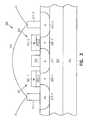
- FIG. 4Ais a cross-sectional view illustrating an embodiment of a pair of memory cells, or merged MOS-bipolar capacitor gain cells, 401 - 1 and 401 - 2 , according to the teachings of the present invention.
- the embodiment of the merged MOS-bipolar capacitor gain cells, 401 - 1 and 401 - 2 , in FIG. 4Adiffer from those shown in FIG. 3 in that the transistors are vertical.
- the memory cells, 401 - 1 and 401 - 2 , of the present inventiondiffer from those described in the above referenced copending, commonly assigned application, entitled “Single Transistor Vertical Memory Gain Cell,” serial number 10/231,397. in that here rather than avalanche breakdown being utilized to store charge on the floating body of a MOS transistor charge is injected on to the body by bipolar transistor action.
- each merged MOS-bipolar capacitor gain cell, 401 - 1 and 401 - 2 , along a row of an arrayis formed on an n+ conductivity type emitter line 407 formed on a p-type substrate 409 .
- the vertically merged MOS-bipolar capacitor gain cells 401 - 1 and 401 - 2include an n+ emitter region for the merged MOS-bipolar structure, 408 - 1 and 408 - 2 respectively.
- the n+ emitter region, 408 - 1 and 408 - 2is integrally formed with the emitter line 407 .
- a p-type conductivity material, 411 - 1 and 411 - 2is formed vertically on the n+ emitter region, 408 - 1 and 408 - 2 .
- the ptype conductivity material, 411 - 1 and 411 - 2serves a dual role. That is, the p-type conductivity material, 411 - 1 and 411 - 2 , serves as a base region for the bipolar device and a source region of the MOS device for the merged MOS-bipolar structure. In this manner, the base region of the bipolar device and the source region of the MOS device are electrically coupled to one another.
- the p-type conductivity material, 411 - 1 and 411 - 2includes a connection (not shown) to a “write data word line” along columns in the array.
- the “write data word lineis operable to bias the base region function of the bipolar device of the merged MOS-bipolar structure.
- an n-type conductivity material, 413 - 1 and 413 - 2is formed vertically on the p-type conductivity material, 411 - 1 and 411 - 2 .
- the n-type conductivity material, 413 - 1 and 413 - 2serves a dual role. That is, the n-type conductivity material, 413 - 1 and 413 - 2 , serves as a collector region for the bipolar device and a body region of the MOS device for the merged MOS-bipolar structure. In this manner, the collector region of the bipolar device and the body region of the MOS device are electrically coupled to one another.
- a p+ type conductivity material, 415 - 1 and 415 - 2is formed vertically on the n-type conductivity material, 413 - 1 and 413 - 2 .
- the n-type conductivity material, 413 - 1 and 413 - 2and serve as the drain regions for the MOS device of the merged MOS-bipolar structure.
- a data/bit line 417couples to the drain regions, 415 - 1 and 415 - 2 , along rows of an array.
- a body capacitor, 403 - 1 and 403 - 2 , and body capacitor plate, 405 - 1 and 405 - 2oppose the collector/body region 413 - 1 and 413 - 2 on one side of the vertical merged MOS-bipolar capacitor memory gain cells, 401 - 1 and 401 - 2 .
- a gate, 419 - 1 and 419 - 2is formed on another side of the vertical merged MOS-bipolar capacitor memory gain cells, 401 - 1 and 401 - 2 from the body capacitor, 403 - 1 and 403 - 2 , and body capacitor plate, 405 - 1 and 405 - 2 .
- FIG. 4Billustrates an electrical equivalent circuit for one of the pair of memory cells, or merged MOS-bipolar capacitor gain cells, 401 - 1 and 401 - 2 shown in FIG. 4 A.
- “read data word line” 421 - 1is shown connected to gate 419 - 1 .
- the merged deviceconsists of a MOS transistor-bipolar transistor-storage capacitor.
- the sense device used to read the cell, e.g. cell 401 - 1is the PMOS transistor, e.g. 402 - 1 which is addressed by the read data word line 421 - 1 .
- the body 413 - 1In operation, if negative charge or electrons are stored on the body 413 - 1 , then the body will be slightly forward biased and the PMOS transistor 402 - 1 will be more conductive than normal. Charge is injected on to the floating body 413 - 1 of the PMOS transistor 402 - 1 by the N+—P—N vertical bipolar transistor, e.g. 409 - 1 .
- the NPN transistor 409 - 1need not be a high performance device nor have a high current gain. In the various embodiments, the NPN transistor 409 - 1 can be a basic, high yield structure.
- Forward biascan be achieved by driving the emitter/sourceline 407 negative and by driving the write data word line 432 , connected to the base/source region 411 - 1 , positive to achieve a coincident address at one location. This is illustrated in more detail in the schematic embodiment shown in FIG. 4 D.
- the cell, 401 - 1can be erased by driving the drain 415 - 1 positive and by driving the gate 419 - 1 negative to forward bias the drain-body p-n junction.
- FIG. 4Cillustrates an embodiment for another mode of operation for a vertical merged MOS-bipolar-capacitor memory gain cell, e.g. 401 - 1 , according to the teachings of the present invention.
- the embodimentallows provisions for biasing a body capacitor plate line 431 to a positive potential.
- biasing a body capacitor plate line 431can be used in conjunction with a positive read data word line 419 - 1 voltage to drive the n-type body 413 - 1 and the p-type source and drain, 411 - 1 and 415 - 1 respectively, junctions to a larger reverse bias during standby. This insures the floating body 413 - 1 will not become forward biased during standby. Thus, stored charge will not be lost due to leakage currents with forward bias.
- FIG. 5is a block diagram of a processor-based system 500 utilizing vertical merged MOS-bipolar-capacitor memory gain cell according to the various embodiments of the present invention. That is, the system 500 utilizes various embodiments of the memory cell illustrated in FIGS. 4A-4D .
- the processor-based system 500may be a computer system, a process control system or any other system employing a processor and associated memory.
- the system 500includes a central processing unit (CPU) 502 , e.g., a microprocessor, that communicates with the RAM 512 and an I/O device 508 over a bus 520 .
- CPUcentral processing unit
- bus 520may be a series of buses and bridges commonly used in a processor-based system, but for convenience purposes only, the bus 520 has been illustrated as a single bus.
- a second I/O device 510is illustrated, but is not necessary to practice the invention.
- the processor-based system 500also includes read-only memory (ROM) 514 and may include peripheral devices such as a floppy disk drive 504 and a compact disk (CD) ROM drive 506 that also communicates with the CPU 502 over the bus 520 as is well known in the art.
- ROMread-only memory
- CDcompact disk
- FIG. 5illustrates an embodiment for electronic system circuitry in which the novel memory cells of the present invention are used.
- the illustration of system 500is intended to provide a general understanding of one application for the structure and circuitry of the present invention, and is not intended to serve as a complete description of all the elements and features of an electronic system using the novel memory cell structures. Further, the invention is equally applicable to any size and type of system 500 using the novel memory cells of the present invention and is not intended to be limited to that described above.
- such an electronic systemcan be fabricated in single-package processing units, or even on a single semiconductor chip, in order to reduce the communication time between the processor and the memory device.
- Applications containing the novel memory cell of the present invention as described in this disclosureinclude electronic systems for use in memory modules, device drivers, power modules, communication modems, processor modules, and application-specific modules, and may include multilayer, multichip modules.
- Such circuitrycan further be a subcomponent of a variety of electronic systems, such as a clock, a television, a cell phone, a personal computer, an automobile, an industrial control system, an aircraft, and others.
- FIG. 6Aoutlines one embodiment of a fabrication technique for merged MOS-bipolar-capacitor memory gain cells where the ernitter/sourceline 602 are separated and can be biased.
- a p-type substrate 601has been processed to include layers thereon of an n+ conductivity type 602 , a p conductivity type 603 , an n conductivity type 604 , and a p+ conductivity type 605 .
- the fabricationcontinues with the wafer being oxidized and then a silicon nitride layer (not shown) is deposited to act as an etch mask for an anisotropic or directional silicon etch which will follow.
- This nitride mask and underlying oxideare patterned and trenches are etched as shown in both directions leaving blocks of silicon, e.g. 600 - 1 , 600 - 2 , 600 - 3 , and 600 - 4 , having alternating layers of n and p type conductivity material. Any number of such blocks can be formed on the wafer.
- two masking stepsare used and one set of trenches, e.g. trench 610 , is made deeper than the other, e.g. trench 609 , in order to provide separation and isolation of the emitter/source lines 602 .
- FIG. 6Billustrates a perspective view taken at cut line 6 B— 6 B from FIG. 6 A.
- both trenches 609 and 610are filled with oxide 607 and the whole structure is planarized such as by CMP.
- the oxide 615 in the write data word line blocks, trench 610are recessed to near the bottom and just above the bottom of the p-type regions 603 in the pillars, 600 - 1 , 600 - 2 , 600 - 2 , and 600 - 4 .
- p-type polysilicon 615is deposited and planarized to be level with the tops of the pillars and then recessed to just below the top of the p-type regions 603 in the pillars, 600 - 1 , 600 - 2 , 600 - 3 , and 600 - 4 .
- This p-type poly 615 and the p-type regions 603 in the pillars 600 - 1 , 600 - 1 , 600 - 3 , and 600 - 4will form the write data word lines, shown as 432 in FIGS. 4B and 4C .
- oxideis again deposited and then planarized to the top of the pillars.
- oxideis again deposited and then planarized to the top of the pillars.
- the trenches 609 for the read data word lines, shown as 421 - 1 in FIGS. 4B and 4C , and the capacitor plate lines, shown 431 in FIG. 4Care opened.
- FIG. 6Dillustrates a cross-sectional view taken along cut line 6 D— 6 D in FIG. 6 C.
- This remaining structurecan then be continued by conventional techniques including gate oxidation and deposition and anisotropic etch of polysilicon along the sidewalls to form body capacitor plate, e.g. 405 - 1 in FIGS. 4A-4C , and read data word lines, e.g. 421 - 1 in FIGS. 4B and 4C .
- the data or bit lines, 417 in FIGS. 4A-4Con top can be realized using conventional metallurgy.
- the vertical merged MOS-bipolar-capacitor memory gain cell 401 - 1 of the present inventioncan provide a very high gain and amplification of the stored charge on the floating body 413 - 1 of the PMOS sense transistor 402 - 1 .
- a small change in the threshold voltage caused by charge stored on the floating body 413 - 1will result in a large difference in the number of holes conducted between the drain 415 - 1 and source 411 - 1 of the PMOS sense transistor 402 - 1 during the read data operation.
- This amplificationallows the small storage capacitance of the sense amplifier floating body 413 - 1 to be used instead of a large stacked capacitor storage capacitance.
- the resulting cell 401 - 1has a very high density with a cell area of 4F 2 , where F is the minimum feature size, and whose vertical extent is far less than the total height of a stacked capacitor or trench capacitor cell and access transistor.
- the sense transistorwould be a PMOS transistor with an ntype floating body.
- the cellcan provide a very high gain and amplification of the stored charge on the floating body of the PMOS sense transistor.
- a small change in the threshold voltage caused by charge stored on the floating bodywill result in a large difference in the number of holes conducted between the drain and source of the PMOS sense transistor during the read data operation.
- This amplificationallows the small storage capacitance of the sense amplifier floating body to be used instead of a large stacked capacitor storage capacitance.
- the resulting cellhas a very high density with a cell area of 4F 2 , where F is the minimum feature size, and whose vertical extent is far less than the total height of a stacked capacitor or trench capacitor cell and access transistor.
Landscapes
- Engineering & Computer Science (AREA)
- Microelectronics & Electronic Packaging (AREA)
- Computer Hardware Design (AREA)
- Semiconductor Memories (AREA)
- Dram (AREA)
Abstract
Description
Claims (42)
Priority Applications (6)
| Application Number | Priority Date | Filing Date | Title |
|---|---|---|---|
| US10/230,929US6838723B2 (en) | 2002-08-29 | 2002-08-29 | Merged MOS-bipolar capacitor memory cell |
| US10/990,586US6940761B2 (en) | 2002-08-29 | 2004-11-17 | Merged MOS-bipolar capacitor memory cell |
| US10/990,713US6943083B2 (en) | 2002-08-29 | 2004-11-17 | Merged MOS-bipolar capacitor memory cell |
| US11/176,992US7199417B2 (en) | 2002-08-29 | 2005-07-08 | Merged MOS-bipolar capacitor memory cell |
| US11/452,025US7608876B2 (en) | 2002-08-29 | 2006-06-13 | Merged MOS-bipolar capacitor memory cell |
| US11/451,920US7564087B2 (en) | 2002-08-29 | 2006-06-13 | Merged MOS-bipolar capacitor memory cell |
Applications Claiming Priority (1)
| Application Number | Priority Date | Filing Date | Title |
|---|---|---|---|
| US10/230,929US6838723B2 (en) | 2002-08-29 | 2002-08-29 | Merged MOS-bipolar capacitor memory cell |
Related Child Applications (2)
| Application Number | Title | Priority Date | Filing Date |
|---|---|---|---|
| US10/990,586DivisionUS6940761B2 (en) | 2002-08-29 | 2004-11-17 | Merged MOS-bipolar capacitor memory cell |
| US10/990,713DivisionUS6943083B2 (en) | 2002-08-29 | 2004-11-17 | Merged MOS-bipolar capacitor memory cell |
Publications (2)
| Publication Number | Publication Date |
|---|---|
| US20040041236A1 US20040041236A1 (en) | 2004-03-04 |
| US6838723B2true US6838723B2 (en) | 2005-01-04 |
Family
ID=31976631
Family Applications (6)
| Application Number | Title | Priority Date | Filing Date |
|---|---|---|---|
| US10/230,929Expired - LifetimeUS6838723B2 (en) | 2002-08-29 | 2002-08-29 | Merged MOS-bipolar capacitor memory cell |
| US10/990,586Expired - LifetimeUS6940761B2 (en) | 2002-08-29 | 2004-11-17 | Merged MOS-bipolar capacitor memory cell |
| US10/990,713Expired - LifetimeUS6943083B2 (en) | 2002-08-29 | 2004-11-17 | Merged MOS-bipolar capacitor memory cell |
| US11/176,992Expired - LifetimeUS7199417B2 (en) | 2002-08-29 | 2005-07-08 | Merged MOS-bipolar capacitor memory cell |
| US11/451,920Expired - LifetimeUS7564087B2 (en) | 2002-08-29 | 2006-06-13 | Merged MOS-bipolar capacitor memory cell |
| US11/452,025Expired - LifetimeUS7608876B2 (en) | 2002-08-29 | 2006-06-13 | Merged MOS-bipolar capacitor memory cell |
Family Applications After (5)
| Application Number | Title | Priority Date | Filing Date |
|---|---|---|---|
| US10/990,586Expired - LifetimeUS6940761B2 (en) | 2002-08-29 | 2004-11-17 | Merged MOS-bipolar capacitor memory cell |
| US10/990,713Expired - LifetimeUS6943083B2 (en) | 2002-08-29 | 2004-11-17 | Merged MOS-bipolar capacitor memory cell |
| US11/176,992Expired - LifetimeUS7199417B2 (en) | 2002-08-29 | 2005-07-08 | Merged MOS-bipolar capacitor memory cell |
| US11/451,920Expired - LifetimeUS7564087B2 (en) | 2002-08-29 | 2006-06-13 | Merged MOS-bipolar capacitor memory cell |
| US11/452,025Expired - LifetimeUS7608876B2 (en) | 2002-08-29 | 2006-06-13 | Merged MOS-bipolar capacitor memory cell |
Country Status (1)
| Country | Link |
|---|---|
| US (6) | US6838723B2 (en) |
Cited By (14)
| Publication number | Priority date | Publication date | Assignee | Title |
|---|---|---|---|---|
| US20040042256A1 (en)* | 2002-08-29 | 2004-03-04 | Micron Technology, Inc. | Single transistor vertical memory gain cell |
| US20050024936A1 (en)* | 2003-03-04 | 2005-02-03 | Micron Technology, Inc. | Vertical gain cell |
| US20050265069A1 (en)* | 2002-08-29 | 2005-12-01 | Micron Technology, Inc. | Merged mos-bipolar capacitor memory cell |
| US20060013042A1 (en)* | 2004-07-19 | 2006-01-19 | Micron Technology, Inc. | In-service reconfigurable dram and flash memory device |
| US20060049392A1 (en)* | 2002-10-08 | 2006-03-09 | Stmicroelectronics S.R.L. | Process for manufacturing an array of cells including selection bipolar junction transistors |
| US7030436B2 (en) | 2002-12-04 | 2006-04-18 | Micron Technology, Inc. | Embedded DRAM gain memory cell having MOS transistor body provided with a bi-polar transistor charge injecting means |
| US7209384B1 (en) | 2005-12-08 | 2007-04-24 | Juhan Kim | Planar capacitor memory cell and its applications |
| US20080012051A1 (en)* | 2006-07-13 | 2008-01-17 | Cho Hyun-Jin | Dynamic Random Access Memory with an Amplified Capacitor |
| US20080031036A1 (en)* | 2006-08-02 | 2008-02-07 | Cho Hyun-Jin | Semiconductor Switching Device |
| US20100176451A1 (en)* | 2009-01-09 | 2010-07-15 | Hoon Jeong | Semiconductor |
| US20110007541A1 (en)* | 2005-06-20 | 2011-01-13 | Scheuerlein Roy E | Floating body memory cell system and method of manufacture |
| KR101091010B1 (en) | 2010-12-17 | 2011-12-08 | 서울대학교산학협력단 | DRAM Device with 2-Bit Storage Single Transistor Structure |
| US20120220091A1 (en)* | 2003-05-20 | 2012-08-30 | Ashok Challa | Methods of making power semiconductor devices with thick bottom oxide layer |
| US20170229486A1 (en)* | 2016-02-05 | 2017-08-10 | Semiconductor Energy Laboratory Co., Ltd. | Semiconductor device and electronic device |
Families Citing this family (66)
| Publication number | Priority date | Publication date | Assignee | Title |
|---|---|---|---|---|
| DE60217120T2 (en)* | 2002-10-08 | 2007-10-25 | Stmicroelectronics S.R.L., Agrate Brianza | A cell assembly having a select bipolar transistor therein and a method of fabricating the same |
| US6804142B2 (en)* | 2002-11-12 | 2004-10-12 | Micron Technology, Inc. | 6F2 3-transistor DRAM gain cell |
| KR100585111B1 (en)* | 2003-11-24 | 2006-06-01 | 삼성전자주식회사 | Non-planar transistors having germanium channel regions and manufacturing methods thereof |
| US7547945B2 (en) | 2004-09-01 | 2009-06-16 | Micron Technology, Inc. | Transistor devices, transistor structures and semiconductor constructions |
| DE102004055183B3 (en)* | 2004-11-16 | 2006-07-13 | Atmel Germany Gmbh | Integrated circuit and method for manufacturing an integrated circuit on a semiconductor chip |
| KR100623618B1 (en)* | 2005-03-31 | 2006-09-14 | 주식회사 하이닉스반도체 | Low Voltage Semiconductor Memory Device |
| FR2884346A1 (en)* | 2005-04-11 | 2006-10-13 | St Microelectronics Sa | Integrated circuit, has one time programmable type memory device with memory cells, each comprising bipolar transistor buried in substrate, and fusible unit made of dielectric material that undergoes breakdown in irreversible manner |
| US7282401B2 (en) | 2005-07-08 | 2007-10-16 | Micron Technology, Inc. | Method and apparatus for a self-aligned recessed access device (RAD) transistor gate |
| US7867851B2 (en) | 2005-08-30 | 2011-01-11 | Micron Technology, Inc. | Methods of forming field effect transistors on substrates |
| KR100675297B1 (en)* | 2005-12-19 | 2007-01-29 | 삼성전자주식회사 | Semiconductor memory device having a capacitorless dynamic memory cell and arrangement method thereof |
| US7700441B2 (en) | 2006-02-02 | 2010-04-20 | Micron Technology, Inc. | Methods of forming field effect transistors, methods of forming field effect transistor gates, methods of forming integrated circuitry comprising a transistor gate array and circuitry peripheral to the gate array, and methods of forming integrated circuitry comprising a transistor gate array including first gates and second grounded isolation gates |
| US7602001B2 (en)* | 2006-07-17 | 2009-10-13 | Micron Technology, Inc. | Capacitorless one transistor DRAM cell, integrated circuitry comprising an array of capacitorless one transistor DRAM cells, and method of forming lines of capacitorless one transistor DRAM cells |
| US7772632B2 (en) | 2006-08-21 | 2010-08-10 | Micron Technology, Inc. | Memory arrays and methods of fabricating memory arrays |
| US7589995B2 (en) | 2006-09-07 | 2009-09-15 | Micron Technology, Inc. | One-transistor memory cell with bias gate |
| WO2009038594A2 (en)* | 2007-01-10 | 2009-03-26 | Brett Blackman | Use of an in vitro hemodynamic endothelial/smooth muscle cell co-culture model to identify new therapeutic targets for vascular disease |
| US7923373B2 (en) | 2007-06-04 | 2011-04-12 | Micron Technology, Inc. | Pitch multiplication using self-assembling materials |
| US7834403B2 (en)* | 2007-08-13 | 2010-11-16 | Infineon Technologies Ag | Bipolar transistor FINFET technology |
| KR100894683B1 (en)* | 2007-08-28 | 2009-04-24 | 경북대학교 산학협력단 | High Performance Single Transistor Floating Body DRAM Device and Manufacturing Method Thereof |
| US7948008B2 (en)* | 2007-10-26 | 2011-05-24 | Micron Technology, Inc. | Floating body field-effect transistors, and methods of forming floating body field-effect transistors |
| US8546876B2 (en) | 2008-03-20 | 2013-10-01 | Micron Technology, Inc. | Systems and devices including multi-transistor cells and methods of using, making, and operating the same |
| US7969776B2 (en) | 2008-04-03 | 2011-06-28 | Micron Technology, Inc. | Data cells with drivers and methods of making and operating the same |
| TWI368299B (en)* | 2008-08-15 | 2012-07-11 | Nanya Technology Corp | Vertical transistor and array of vertical transistor |
| US7847373B2 (en)* | 2008-12-22 | 2010-12-07 | Agostino Pirovano | Fabricating bipolar junction select transistors for semiconductor memories |
| US8081502B1 (en) | 2008-12-29 | 2011-12-20 | Altera Corporation | Memory elements with body bias control |
| US8748959B2 (en)* | 2009-03-31 | 2014-06-10 | Micron Technology, Inc. | Semiconductor memory device |
| JP4487221B1 (en)* | 2009-04-17 | 2010-06-23 | 日本ユニサンティスエレクトロニクス株式会社 | Semiconductor device |
| CN101635298B (en)* | 2009-06-10 | 2014-12-31 | 北京中星微电子有限公司 | Three-dimensional integrated circuit of planar technology |
| EP2320454A1 (en)* | 2009-11-05 | 2011-05-11 | S.O.I.Tec Silicon on Insulator Technologies | Substrate holder and clipping device |
| FR2953643B1 (en)* | 2009-12-08 | 2012-07-27 | Soitec Silicon On Insulator | MEMORY CELL FLASH ON SEOI HAVING A SECOND CHECK GRID ENTERREE UNDER THE INSULATING LAYER |
| FR2957193B1 (en) | 2010-03-03 | 2012-04-20 | Soitec Silicon On Insulator | SEOI SUBSTRATE DATA PATH CELL WITH REAR CONTROL GRID BURED UNDER THE INSULATING LAYER |
| FR2953636B1 (en)* | 2009-12-08 | 2012-02-10 | Soitec Silicon On Insulator | METHOD FOR CONTROLLING A DRAM MEMORY CELL ON SEOI HAVING A SECOND BURST CONTROL GRID UNDER THE INSULATING LAYER |
| US8508289B2 (en)* | 2009-12-08 | 2013-08-13 | Soitec | Data-path cell on an SeOI substrate with a back control gate beneath the insulating layer |
| FR2953641B1 (en)* | 2009-12-08 | 2012-02-10 | S O I Tec Silicon On Insulator Tech | HOMOGENEOUS TRANSISTOR CIRCUIT ON SEOI WITH REAR CONTROL CHANNEL BURED UNDER THE INSULATING LAYER |
| FR2955204B1 (en)* | 2010-01-14 | 2012-07-20 | Soitec Silicon On Insulator | DRAM MEMORY CELL HAVING A VERTICAL BIPOLAR INJECTOR |
| FR2955195B1 (en)* | 2010-01-14 | 2012-03-09 | Soitec Silicon On Insulator | DEVICE FOR COMPARING DATA IN A MEMORY ADDRESSABLE BY CONTENT ON SEOI |
| FR2955203B1 (en)* | 2010-01-14 | 2012-03-23 | Soitec Silicon On Insulator | MEMORY CELL WITH THE CHANNEL CROSSING A DIELECTRIC LAYER ENTERREE |
| FR2955200B1 (en) | 2010-01-14 | 2012-07-20 | Soitec Silicon On Insulator | DEVICE AND MANUFACTURING METHOD HAVING CONTACT BETWEEN SEMICONDUCTOR REGIONS THROUGH AN INSULATED INSULATED LAYER |
| US9646869B2 (en) | 2010-03-02 | 2017-05-09 | Micron Technology, Inc. | Semiconductor devices including a diode structure over a conductive strap and methods of forming such semiconductor devices |
| US8513722B2 (en) | 2010-03-02 | 2013-08-20 | Micron Technology, Inc. | Floating body cell structures, devices including same, and methods for forming same |
| US9608119B2 (en) | 2010-03-02 | 2017-03-28 | Micron Technology, Inc. | Semiconductor-metal-on-insulator structures, methods of forming such structures, and semiconductor devices including such structures |
| US8507966B2 (en) | 2010-03-02 | 2013-08-13 | Micron Technology, Inc. | Semiconductor cells, arrays, devices and systems having a buried conductive line and methods for forming the same |
| US8288795B2 (en) | 2010-03-02 | 2012-10-16 | Micron Technology, Inc. | Thyristor based memory cells, devices and systems including the same and methods for forming the same |
| FR2957186B1 (en)* | 2010-03-08 | 2012-09-28 | Soitec Silicon On Insulator | MEMORY CELL OF SRAM TYPE |
| FR2957449B1 (en) | 2010-03-11 | 2022-07-15 | S O I Tec Silicon On Insulator Tech | READOUT MICRO-AMPLIFIER FOR MEMORY |
| FR2958441B1 (en) | 2010-04-02 | 2012-07-13 | Soitec Silicon On Insulator | PSEUDO-INVERTER CIRCUIT ON SEOI |
| EP2375442A1 (en) | 2010-04-06 | 2011-10-12 | S.O.I.Tec Silicon on Insulator Technologies | Method for manufacturing a semiconductor substrate |
| EP2381470B1 (en) | 2010-04-22 | 2012-08-22 | Soitec | Semiconductor device comprising a field-effect transistor in a silicon-on-insulator structure |
| RU2444806C2 (en)* | 2010-05-19 | 2012-03-10 | Государственное образовательное учреждение высшего профессионального образования "Московский государственный институт электроники и математики (технический университет)" | Memory cell based on thin-layer nanostructure |
| US8535992B2 (en)* | 2010-06-29 | 2013-09-17 | Micron Technology, Inc. | Thyristor random access memory device and method |
| KR101085155B1 (en) | 2010-11-16 | 2011-11-18 | 서강대학교산학협력단 | 1T DRAM Cell Device Using Tunneling Field Effect Transistor |
| KR101105712B1 (en) | 2010-12-13 | 2012-01-17 | 서울대학교산학협력단 | Memory cell structure of capacitorless DRAM |
| US8598621B2 (en) | 2011-02-11 | 2013-12-03 | Micron Technology, Inc. | Memory cells, memory arrays, methods of forming memory cells, and methods of forming a shared doped semiconductor region of a vertically oriented thyristor and a vertically oriented access transistor |
| US8952418B2 (en)* | 2011-03-01 | 2015-02-10 | Micron Technology, Inc. | Gated bipolar junction transistors |
| US8519431B2 (en) | 2011-03-08 | 2013-08-27 | Micron Technology, Inc. | Thyristors |
| US8772848B2 (en) | 2011-07-26 | 2014-07-08 | Micron Technology, Inc. | Circuit structures, memory circuitry, and methods |
| KR101155451B1 (en) | 2011-08-31 | 2012-06-15 | 테세라, 인코포레이티드 | Dram security erase |
| KR101221445B1 (en) | 2012-04-20 | 2013-01-11 | 한국과학기술원 | Capacitorless dynamic landom access memory and fabrication method thereof |
| US8946018B2 (en)* | 2012-08-21 | 2015-02-03 | Micron Technology, Inc. | Methods of forming memory arrays and semiconductor constructions |
| CN117136637A (en)* | 2021-06-29 | 2023-11-28 | 华为技术有限公司 | Memory and formation method thereof, electronic equipment |
| CN116234296B (en)* | 2022-01-18 | 2024-09-17 | 北京超弦存储器研究院 | Dynamic memory and SOC chip |
| CN116234298B (en)* | 2022-01-26 | 2024-02-23 | 北京超弦存储器研究院 | Dynamic memory and SOC chip |
| CN116209244B (en)* | 2022-01-26 | 2024-02-23 | 北京超弦存储器研究院 | Dynamic memory and memory device |
| CN116234299B (en)* | 2022-01-27 | 2024-02-23 | 北京超弦存储器研究院 | Dynamic memory, manufacturing method thereof and SOC chip |
| WO2023188006A1 (en)* | 2022-03-29 | 2023-10-05 | ユニサンティス エレクトロニクス シンガポール プライベート リミテッド | Semiconductor memory device |
| US20240049476A1 (en)* | 2022-08-06 | 2024-02-08 | Euipil Kwon | Semiconducor device and method of fabricating the same |
| CN118317603B (en)* | 2024-04-10 | 2024-09-27 | 北京超弦存储器研究院 | Semiconductor device, method of manufacturing the same, and electronic apparatus |
Citations (58)
| Publication number | Priority date | Publication date | Assignee | Title |
|---|---|---|---|---|
| JPS61140170A (en) | 1984-12-13 | 1986-06-27 | Toshiba Corp | semiconductor storage device |
| US4826780A (en) | 1982-04-19 | 1989-05-02 | Matsushita Electric Industrial Co., Ltd. | Method of making bipolar transistors |
| US4970689A (en) | 1988-03-07 | 1990-11-13 | International Business Machines Corporation | Charge amplifying trench memory cell |
| US4999811A (en) | 1987-11-30 | 1991-03-12 | Texas Instruments Incorporated | Trench DRAM cell with dynamic gain |
| US5006909A (en) | 1989-10-30 | 1991-04-09 | Motorola, Inc. | Dram with a vertical capacitor and transistor |
| US5017504A (en) | 1986-12-01 | 1991-05-21 | Mitsubishi Denki Kabushiki Kaisha | Vertical type MOS transistor and method of formation thereof |
| US5021355A (en) | 1989-05-22 | 1991-06-04 | International Business Machines Corporation | Method of fabricating cross-point lightly-doped drain-source trench transistor |
| US5042011A (en) | 1989-05-22 | 1991-08-20 | Micron Technology, Inc. | Sense amplifier pulldown device with tailored edge input |
| US5066607A (en) | 1987-11-30 | 1991-11-19 | Texas Instruments Incorporated | Method of making a trench DRAM cell with dynamic gain |
| US5078798A (en) | 1989-12-28 | 1992-01-07 | Ciba-Geigy Corporation | Buoyancy mediated control of catalytic reaction |
| US5122986A (en) | 1990-11-21 | 1992-06-16 | Micron Technology, Inc. | Two transistor dram cell |
| US5220530A (en) | 1990-08-07 | 1993-06-15 | Oki Electric Industry Co., Ltd. | Semiconductor memory element and method of fabricating the same |
| JPH05226661A (en) | 1992-02-17 | 1993-09-03 | Mitsubishi Electric Corp | Semiconductor device and manufacturing method thereof |
| US5280205A (en) | 1992-04-16 | 1994-01-18 | Micron Technology, Inc. | Fast sense amplifier |
| US5291438A (en) | 1992-03-23 | 1994-03-01 | Motorola, Inc. | Transistor and a capacitor used for forming a vertically stacked dynamic random access memory cell |
| US5308783A (en) | 1992-12-16 | 1994-05-03 | Siemens Aktiengesellschaft | Process for the manufacture of a high density cell array of gain memory cells |
| US5378914A (en) | 1990-05-31 | 1995-01-03 | Canon Kabushiki Kaisha | Semiconductor device with a particular source/drain and gate structure |
| US5381302A (en) | 1993-04-02 | 1995-01-10 | Micron Semiconductor, Inc. | Capacitor compatible with high dielectric constant materials having a low contact resistance layer and the method for forming same |
| US5385853A (en) | 1992-12-02 | 1995-01-31 | International Business Machines Corporation | Method of fabricating a metal oxide semiconductor heterojunction field effect transistor (MOSHFET) |
| US5414288A (en) | 1992-11-19 | 1995-05-09 | Motorola, Inc. | Vertical transistor having an underlying gate electrode contact |
| US5448513A (en) | 1993-12-02 | 1995-09-05 | Regents Of The University Of California | Capacitorless DRAM device on silicon-on-insulator substrate |
| US5478772A (en) | 1993-04-02 | 1995-12-26 | Micron Technology, Inc. | Method for forming a storage cell capacitor compatible with high dielectric constant materials |
| US5519236A (en) | 1993-06-28 | 1996-05-21 | Kabushiki Kaisha Toshiba | Semiconductor memory device having surrounding gate transistor |
| US5574299A (en) | 1994-03-28 | 1996-11-12 | Samsung Electronics Co., Ltd. | Semiconductor device having vertical conduction transistors and cylindrical cell gates |
| US5627785A (en) | 1996-03-15 | 1997-05-06 | Micron Technology, Inc. | Memory device with a sense amplifier |
| US5707885A (en) | 1995-05-26 | 1998-01-13 | Samsung Electronics Co., Ltd. | Method for manufacturing a vertical transistor having a storage node vertical transistor |
| US5719409A (en) | 1996-06-06 | 1998-02-17 | Cree Research, Inc. | Silicon carbide metal-insulator semiconductor field effect transistor |
| US5732014A (en) | 1997-02-20 | 1998-03-24 | Micron Technology, Inc. | Merged transistor structure for gain memory cell |
| US5854500A (en) | 1995-09-26 | 1998-12-29 | Siemens Aktiengesellschaft | DRAM cell array with dynamic gain memory cells |
| US5909618A (en) | 1997-07-08 | 1999-06-01 | Micron Technology, Inc. | Method of making memory cell with vertical transistor and buried word and body lines |
| US5937296A (en) | 1996-12-20 | 1999-08-10 | Siemens Aktiengesellschaft | Memory cell that includes a vertical transistor and a trench capacitor |
| US5936274A (en) | 1997-07-08 | 1999-08-10 | Micron Technology, Inc. | High density flash memory |
| US5973356A (en) | 1997-07-08 | 1999-10-26 | Micron Technology, Inc. | Ultra high density flash memory |
| US5991225A (en) | 1998-02-27 | 1999-11-23 | Micron Technology, Inc. | Programmable memory address decode array with vertical transistors |
| US5999455A (en) | 1998-06-12 | 1999-12-07 | Macronix International Co., Ltd. | Channel FN program/erase recovery scheme |
| US6031263A (en) | 1997-07-29 | 2000-02-29 | Micron Technology, Inc. | DEAPROM and transistor with gallium nitride or gallium aluminum nitride gate |
| US6030847A (en) | 1993-04-02 | 2000-02-29 | Micron Technology, Inc. | Method for forming a storage cell capacitor compatible with high dielectric constant materials |
| US6072209A (en) | 1997-07-08 | 2000-06-06 | Micro Technology, Inc. | Four F2 folded bit line DRAM cell structure having buried bit and word lines |
| US6077745A (en) | 1997-01-22 | 2000-06-20 | International Business Machines Corporation | Self-aligned diffused source vertical transistors with stack capacitors in a 4F-square memory cell array |
| US6097065A (en) | 1998-03-30 | 2000-08-01 | Micron Technology, Inc. | Circuits and methods for dual-gated transistors |
| US6124729A (en) | 1998-02-27 | 2000-09-26 | Micron Technology, Inc. | Field programmable logic arrays with vertical transistors |
| US6150687A (en) | 1997-07-08 | 2000-11-21 | Micron Technology, Inc. | Memory cell having a vertical transistor with buried source/drain and dual gates |
| US6172390B1 (en) | 1998-03-25 | 2001-01-09 | Siemens Aktiengesellschaft | Semiconductor device with vertical transistor and buried word line |
| US6204115B1 (en) | 1999-06-03 | 2001-03-20 | Stanford University | Manufacture of high-density pillar memory cell arrangement |
| US6246083B1 (en)* | 1998-02-24 | 2001-06-12 | Micron Technology, Inc. | Vertical gain cell and array for a dynamic random access memory |
| US6249460B1 (en) | 2000-02-28 | 2001-06-19 | Micron Technology, Inc. | Dynamic flash memory cells with ultrathin tunnel oxides |
| US6282115B1 (en) | 1999-12-22 | 2001-08-28 | International Business Machines Corporation | Multi-level DRAM trench store utilizing two capacitors and two plates |
| US6316309B1 (en) | 1998-06-09 | 2001-11-13 | Steven John Holmes | Method of forming self-isolated and self-aligned 4F-square vertical FET-trench DRAM cells |
| US6384448B1 (en) | 2000-02-28 | 2002-05-07 | Micron Technology, Inc. | P-channel dynamic flash memory cells with ultrathin tunnel oxides |
| US20020098639A1 (en) | 2000-12-28 | 2002-07-25 | Teruaki Kisu | Method of manufacturing semiconductor memory device and semiconductor memory device |
| US6440801B1 (en) | 1997-01-22 | 2002-08-27 | International Business Machines Corporation | Structure for folded architecture pillar memory cell |
| US20030001191A1 (en) | 1997-07-29 | 2003-01-02 | Micron Technology, Inc. | Dynamic electrically alterable programmable read only memory device |
| US6531730B2 (en) | 1993-08-10 | 2003-03-11 | Micron Technology, Inc. | Capacitor compatible with high dielectric constant materials having a low contact resistance layer and the method for forming same |
| US6538916B2 (en) | 2001-02-15 | 2003-03-25 | Kabushiki Kaisha Toshiba | Semiconductor memory device |
| US6566682B2 (en) | 2001-02-09 | 2003-05-20 | Micron Technology, Inc. | Programmable memory address and decode circuits with ultra thin vertical body transistors |
| US6624033B2 (en) | 1998-12-03 | 2003-09-23 | Micron Technology, Inc. | Trench DRAM cell with vertical device and buried word lines |
| US6710465B2 (en) | 2001-06-21 | 2004-03-23 | Samsung Electronics Co., Ltd. | Scalable two transistor memory device |
| US6727141B1 (en) | 2003-01-14 | 2004-04-27 | International Business Machines Corporation | DRAM having offset vertical transistors and method |
Family Cites Families (32)
| Publication number | Priority date | Publication date | Assignee | Title |
|---|---|---|---|---|
| US4130892A (en) | 1977-01-03 | 1978-12-19 | Rockwell International Corporation | Radiation hard memory cell and array thereof |
| US5028977A (en) | 1989-06-16 | 1991-07-02 | Massachusetts Institute Of Technology | Merged bipolar and insulated gate transistors |
| TW289168B (en)* | 1991-12-16 | 1996-10-21 | Philips Nv | |
| US5604201A (en)* | 1993-01-08 | 1997-02-18 | State Of Oregon, Acting By And Through The Oregon State Board Of Higher Education On Behalf Of The Oregon Health Sciences University, A Non-Profit Organization | Methods and reagents for inhibiting furin endoprotease |
| JPH09147598A (en)* | 1995-11-28 | 1997-06-06 | Mitsubishi Electric Corp | Semiconductor memory device and address change detection circuit |
| DE19548060A1 (en) | 1995-12-21 | 1997-06-26 | Siemens Ag | Power semiconductor device with temperature sensor that can be controlled by field effect |
| US5995419A (en) | 1998-06-25 | 1999-11-30 | Xilinx, Inc. | Repairable memory cell for a memory cell array |
| US5815432A (en) | 1997-07-10 | 1998-09-29 | Hewlett-Packard Company | Single-ended read, dual-ended write SCRAM cell |
| JPH1139877A (en)* | 1997-07-15 | 1999-02-12 | Mitsubishi Electric Corp | Semiconductor storage device |
| US5872032A (en)* | 1997-11-03 | 1999-02-16 | Vanguard International Semiconductor Corporation | Fabrication method for a DRAM cell with bipolar charge amplification |
| KR100599130B1 (en) | 1998-03-18 | 2006-07-12 | 코닌클리즈케 필립스 일렉트로닉스 엔.브이. | Semiconductor device with memory cells |
| KR100423765B1 (en) | 1998-09-25 | 2004-03-22 | 인피네온 테크놀로지스 아게 | Integrated circuit comprising vertical transistors, and a method for the production thereof |
| US6111286A (en)* | 1998-10-22 | 2000-08-29 | Worldwide Semiconductor Manufacturing Corporation | Low voltage low power n-channel flash memory cell using gate induced drain leakage current |
| US6213869B1 (en) | 1999-05-10 | 2001-04-10 | Advanced Micro Devices, Inc. | MOSFET-type device with higher driver current and lower steady state power dissipation |
| US6141238A (en) | 1999-08-30 | 2000-10-31 | Micron Technology, Inc. | Dynamic random access memory (DRAM) cells with repressed ferroelectric memory methods of reading same, and apparatuses including same |
| US6172901B1 (en) | 1999-12-30 | 2001-01-09 | Stmicroelectronics, S.R.L. | Low power static random access memory and method for writing to same |
| TW469635B (en) | 2000-05-16 | 2001-12-21 | Nanya Technology Corp | Fabrication method of semiconductor memory cell transistor |
| US6883021B2 (en)* | 2000-09-08 | 2005-04-19 | Quartics, Inc. | Programmable and multiplierless Viterbi accelerator |
| US6625057B2 (en) | 2000-11-17 | 2003-09-23 | Kabushiki Kaisha Toshiba | Magnetoresistive memory device |
| US6560139B2 (en) | 2001-03-05 | 2003-05-06 | Intel Corporation | Low leakage current SRAM array |
| JP4797265B2 (en) | 2001-03-21 | 2011-10-19 | 富士電機株式会社 | Semiconductor device and manufacturing method of semiconductor device |
| US6556471B2 (en) | 2001-06-27 | 2003-04-29 | Intel Corporation | VDD modulated SRAM for highly scaled, high performance cache |
| US6549453B2 (en) | 2001-06-29 | 2003-04-15 | International Business Machines Corporation | Method and apparatus for writing operation in SRAM cells employing PFETS pass gates |
| US6461900B1 (en) | 2001-10-18 | 2002-10-08 | Chartered Semiconductor Manufacturing Ltd. | Method to form a self-aligned CMOS inverter using vertical device integration |
| US6661042B2 (en)* | 2002-03-11 | 2003-12-09 | Monolithic System Technology, Inc. | One-transistor floating-body DRAM cell in bulk CMOS process with electrically isolated charge storage region |
| US6686624B2 (en) | 2002-03-11 | 2004-02-03 | Monolithic System Technology, Inc. | Vertical one-transistor floating-body DRAM cell in bulk CMOS process with electrically isolated charge storage region |
| US6611451B1 (en) | 2002-06-28 | 2003-08-26 | Texas Instruments Incorporated | Memory array and wordline driver supply voltage differential in standby |
| US6838723B2 (en) | 2002-08-29 | 2005-01-04 | Micron Technology, Inc. | Merged MOS-bipolar capacitor memory cell |
| US7224024B2 (en) | 2002-08-29 | 2007-05-29 | Micron Technology, Inc. | Single transistor vertical memory gain cell |
| US6804142B2 (en) | 2002-11-12 | 2004-10-12 | Micron Technology, Inc. | 6F2 3-transistor DRAM gain cell |
| US7030436B2 (en) | 2002-12-04 | 2006-04-18 | Micron Technology, Inc. | Embedded DRAM gain memory cell having MOS transistor body provided with a bi-polar transistor charge injecting means |
| US6956256B2 (en) | 2003-03-04 | 2005-10-18 | Micron Technology Inc. | Vertical gain cell |
- 2002
- 2002-08-29USUS10/230,929patent/US6838723B2/ennot_activeExpired - Lifetime
- 2004
- 2004-11-17USUS10/990,586patent/US6940761B2/ennot_activeExpired - Lifetime
- 2004-11-17USUS10/990,713patent/US6943083B2/ennot_activeExpired - Lifetime
- 2005
- 2005-07-08USUS11/176,992patent/US7199417B2/ennot_activeExpired - Lifetime
- 2006
- 2006-06-13USUS11/451,920patent/US7564087B2/ennot_activeExpired - Lifetime
- 2006-06-13USUS11/452,025patent/US7608876B2/ennot_activeExpired - Lifetime
Patent Citations (83)
| Publication number | Priority date | Publication date | Assignee | Title |
|---|---|---|---|---|
| US4826780A (en) | 1982-04-19 | 1989-05-02 | Matsushita Electric Industrial Co., Ltd. | Method of making bipolar transistors |
| JPS61140170A (en) | 1984-12-13 | 1986-06-27 | Toshiba Corp | semiconductor storage device |
| US5017504A (en) | 1986-12-01 | 1991-05-21 | Mitsubishi Denki Kabushiki Kaisha | Vertical type MOS transistor and method of formation thereof |
| US4999811A (en) | 1987-11-30 | 1991-03-12 | Texas Instruments Incorporated | Trench DRAM cell with dynamic gain |
| US5066607A (en) | 1987-11-30 | 1991-11-19 | Texas Instruments Incorporated | Method of making a trench DRAM cell with dynamic gain |
| US4970689A (en) | 1988-03-07 | 1990-11-13 | International Business Machines Corporation | Charge amplifying trench memory cell |
| US5021355A (en) | 1989-05-22 | 1991-06-04 | International Business Machines Corporation | Method of fabricating cross-point lightly-doped drain-source trench transistor |
| US5042011A (en) | 1989-05-22 | 1991-08-20 | Micron Technology, Inc. | Sense amplifier pulldown device with tailored edge input |
| US5006909A (en) | 1989-10-30 | 1991-04-09 | Motorola, Inc. | Dram with a vertical capacitor and transistor |
| US5078798A (en) | 1989-12-28 | 1992-01-07 | Ciba-Geigy Corporation | Buoyancy mediated control of catalytic reaction |
| US5378914A (en) | 1990-05-31 | 1995-01-03 | Canon Kabushiki Kaisha | Semiconductor device with a particular source/drain and gate structure |
| US5220530A (en) | 1990-08-07 | 1993-06-15 | Oki Electric Industry Co., Ltd. | Semiconductor memory element and method of fabricating the same |
| US5122986A (en) | 1990-11-21 | 1992-06-16 | Micron Technology, Inc. | Two transistor dram cell |
| JPH05226661A (en) | 1992-02-17 | 1993-09-03 | Mitsubishi Electric Corp | Semiconductor device and manufacturing method thereof |
| US5291438A (en) | 1992-03-23 | 1994-03-01 | Motorola, Inc. | Transistor and a capacitor used for forming a vertically stacked dynamic random access memory cell |
| US5280205A (en) | 1992-04-16 | 1994-01-18 | Micron Technology, Inc. | Fast sense amplifier |
| US5414288A (en) | 1992-11-19 | 1995-05-09 | Motorola, Inc. | Vertical transistor having an underlying gate electrode contact |
| US5385853A (en) | 1992-12-02 | 1995-01-31 | International Business Machines Corporation | Method of fabricating a metal oxide semiconductor heterojunction field effect transistor (MOSHFET) |
| US5308783A (en) | 1992-12-16 | 1994-05-03 | Siemens Aktiengesellschaft | Process for the manufacture of a high density cell array of gain memory cells |
| US5478772A (en) | 1993-04-02 | 1995-12-26 | Micron Technology, Inc. | Method for forming a storage cell capacitor compatible with high dielectric constant materials |
| US5381302A (en) | 1993-04-02 | 1995-01-10 | Micron Semiconductor, Inc. | Capacitor compatible with high dielectric constant materials having a low contact resistance layer and the method for forming same |
| US5506166A (en) | 1993-04-02 | 1996-04-09 | Micron Technology, Inc. | Method for forming capacitor compatible with high dielectric constant materials having a low contact resistance layer |
| US6030847A (en) | 1993-04-02 | 2000-02-29 | Micron Technology, Inc. | Method for forming a storage cell capacitor compatible with high dielectric constant materials |
| US5959327A (en) | 1993-04-02 | 1999-09-28 | Micron Technology, Inc. | Capacitor compatible with high dielectric constant materials having a low contact resistance layer and the method for forming same |
| US20030155604A1 (en) | 1993-04-02 | 2003-08-21 | Micron Technology, Inc. | Capacitor compatible with high dielectric constant materials having a low contact resistance layer and the method for forming same |
| US5519236A (en) | 1993-06-28 | 1996-05-21 | Kabushiki Kaisha Toshiba | Semiconductor memory device having surrounding gate transistor |
| US6531730B2 (en) | 1993-08-10 | 2003-03-11 | Micron Technology, Inc. | Capacitor compatible with high dielectric constant materials having a low contact resistance layer and the method for forming same |
| US5448513A (en) | 1993-12-02 | 1995-09-05 | Regents Of The University Of California | Capacitorless DRAM device on silicon-on-insulator substrate |
| US5574299A (en) | 1994-03-28 | 1996-11-12 | Samsung Electronics Co., Ltd. | Semiconductor device having vertical conduction transistors and cylindrical cell gates |
| US5707885A (en) | 1995-05-26 | 1998-01-13 | Samsung Electronics Co., Ltd. | Method for manufacturing a vertical transistor having a storage node vertical transistor |
| US5854500A (en) | 1995-09-26 | 1998-12-29 | Siemens Aktiengesellschaft | DRAM cell array with dynamic gain memory cells |
| US5627785A (en) | 1996-03-15 | 1997-05-06 | Micron Technology, Inc. | Memory device with a sense amplifier |
| US5719409A (en) | 1996-06-06 | 1998-02-17 | Cree Research, Inc. | Silicon carbide metal-insulator semiconductor field effect transistor |
| US5937296A (en) | 1996-12-20 | 1999-08-10 | Siemens Aktiengesellschaft | Memory cell that includes a vertical transistor and a trench capacitor |
| US6077745A (en) | 1997-01-22 | 2000-06-20 | International Business Machines Corporation | Self-aligned diffused source vertical transistors with stack capacitors in a 4F-square memory cell array |
| US6440801B1 (en) | 1997-01-22 | 2002-08-27 | International Business Machines Corporation | Structure for folded architecture pillar memory cell |
| US5732014A (en) | 1997-02-20 | 1998-03-24 | Micron Technology, Inc. | Merged transistor structure for gain memory cell |
| US5897351A (en) | 1997-02-20 | 1999-04-27 | Micron Technology, Inc. | Method for forming merged transistor structure for gain memory cell |
| US5936274A (en) | 1997-07-08 | 1999-08-10 | Micron Technology, Inc. | High density flash memory |
| US6238976B1 (en) | 1997-07-08 | 2001-05-29 | Micron Technology, Inc. | Method for forming high density flash memory |
| US6072209A (en) | 1997-07-08 | 2000-06-06 | Micro Technology, Inc. | Four F2 folded bit line DRAM cell structure having buried bit and word lines |
| US5909618A (en) | 1997-07-08 | 1999-06-01 | Micron Technology, Inc. | Method of making memory cell with vertical transistor and buried word and body lines |
| US5973356A (en) | 1997-07-08 | 1999-10-26 | Micron Technology, Inc. | Ultra high density flash memory |
| US6104061A (en) | 1997-07-08 | 2000-08-15 | Micron Technology, Inc. | Memory cell with vertical transistor and buried word and body lines |
| US6492233B2 (en) | 1997-07-08 | 2002-12-10 | Micron Technology, Inc. | Memory cell with vertical transistor and buried word and body lines |
| US6143636A (en) | 1997-07-08 | 2000-11-07 | Micron Technology, Inc. | High density flash memory |
| US6150687A (en) | 1997-07-08 | 2000-11-21 | Micron Technology, Inc. | Memory cell having a vertical transistor with buried source/drain and dual gates |
| US6504201B1 (en) | 1997-07-08 | 2003-01-07 | Micron Technology, Inc. | Memory cell having a vertical transistor with buried source/drain and dual gates |
| US6399979B1 (en) | 1997-07-08 | 2002-06-04 | Micron Technology, Inc. | Memory cell having a vertical transistor with buried source/drain and dual gates |
| US6191448B1 (en) | 1997-07-08 | 2001-02-20 | Micron Technology, Inc. | Memory cell with vertical transistor and buried word and body lines |
| US6350635B1 (en) | 1997-07-08 | 2002-02-26 | Micron Technology, Inc. | Memory cell having a vertical transistor with buried source/drain and dual gates |
| US20030001191A1 (en) | 1997-07-29 | 2003-01-02 | Micron Technology, Inc. | Dynamic electrically alterable programmable read only memory device |
| US6249020B1 (en) | 1997-07-29 | 2001-06-19 | Micron Technology, Inc. | DEAPROM and transistor with gallium nitride or gallium aluminum nitride gate |
| US20030205754A1 (en) | 1997-07-29 | 2003-11-06 | Micron Technology, Inc. | Dynamic electrically alterable programmable read only memory device |
| US6307775B1 (en) | 1997-07-29 | 2001-10-23 | Micron Technology, Inc. | Deaprom and transistor with gallium nitride or gallium aluminum nitride gate |
| US20010032997A1 (en) | 1997-07-29 | 2001-10-25 | Micron Technology, Inc. | DEAPROM and transistor with gallium nitride or gallium aluminum nitride gate |
| US6031263A (en) | 1997-07-29 | 2000-02-29 | Micron Technology, Inc. | DEAPROM and transistor with gallium nitride or gallium aluminum nitride gate |
| US20020126536A1 (en) | 1997-07-29 | 2002-09-12 | Micron Technology, Inc. | Deaprom and transistor with gallium nitride or gallium aluminum nitride gate |
| US6246083B1 (en)* | 1998-02-24 | 2001-06-12 | Micron Technology, Inc. | Vertical gain cell and array for a dynamic random access memory |
| US6680864B2 (en) | 1998-02-24 | 2004-01-20 | Micron Technology, Inc. | Method for reading a vertical gain cell and array for a dynamic random access memory |
| US20010028078A1 (en) | 1998-02-24 | 2001-10-11 | Micron Technology, Inc. | Vertical gain cell and array for a dynamic random access memory and method for forming the same |
| US20010030338A1 (en) | 1998-02-24 | 2001-10-18 | Micron Technology, Inc. | Vertical gain cell and array for a dynamic random access memory and method for forming the same |
| US6153468A (en) | 1998-02-27 | 2000-11-28 | Micron Technololgy, Inc. | Method of forming a logic array for a decoder |
| US6124729A (en) | 1998-02-27 | 2000-09-26 | Micron Technology, Inc. | Field programmable logic arrays with vertical transistors |
| US5991225A (en) | 1998-02-27 | 1999-11-23 | Micron Technology, Inc. | Programmable memory address decode array with vertical transistors |
| US6172390B1 (en) | 1998-03-25 | 2001-01-09 | Siemens Aktiengesellschaft | Semiconductor device with vertical transistor and buried word line |
| US6097065A (en) | 1998-03-30 | 2000-08-01 | Micron Technology, Inc. | Circuits and methods for dual-gated transistors |
| US6316309B1 (en) | 1998-06-09 | 2001-11-13 | Steven John Holmes | Method of forming self-isolated and self-aligned 4F-square vertical FET-trench DRAM cells |
| US5999455A (en) | 1998-06-12 | 1999-12-07 | Macronix International Co., Ltd. | Channel FN program/erase recovery scheme |
| US6624033B2 (en) | 1998-12-03 | 2003-09-23 | Micron Technology, Inc. | Trench DRAM cell with vertical device and buried word lines |
| US6204115B1 (en) | 1999-06-03 | 2001-03-20 | Stanford University | Manufacture of high-density pillar memory cell arrangement |
| US6282115B1 (en) | 1999-12-22 | 2001-08-28 | International Business Machines Corporation | Multi-level DRAM trench store utilizing two capacitors and two plates |
| US20010053096A1 (en) | 2000-02-28 | 2001-12-20 | Micron Technology, Inc. | Dynamic flash memory cells with ultra thin tunnel oxides |
| US6456535B2 (en) | 2000-02-28 | 2002-09-24 | Micron Technology, Inc. | Dynamic flash memory cells with ultra thin tunnel oxides |
| US6384448B1 (en) | 2000-02-28 | 2002-05-07 | Micron Technology, Inc. | P-channel dynamic flash memory cells with ultrathin tunnel oxides |
| US6249460B1 (en) | 2000-02-28 | 2001-06-19 | Micron Technology, Inc. | Dynamic flash memory cells with ultrathin tunnel oxides |
| US20030129001A1 (en) | 2000-12-28 | 2003-07-10 | Teruaki Kisu | Method of manufacturing semiconductor memory device and semiconductor memory device |
| US20020098639A1 (en) | 2000-12-28 | 2002-07-25 | Teruaki Kisu | Method of manufacturing semiconductor memory device and semiconductor memory device |
| US6501116B2 (en) | 2000-12-28 | 2002-12-31 | Hitachi, Ltd. | Semiconductor memory device with MIS transistors |
| US6566682B2 (en) | 2001-02-09 | 2003-05-20 | Micron Technology, Inc. | Programmable memory address and decode circuits with ultra thin vertical body transistors |
| US6538916B2 (en) | 2001-02-15 | 2003-03-25 | Kabushiki Kaisha Toshiba | Semiconductor memory device |
| US6710465B2 (en) | 2001-06-21 | 2004-03-23 | Samsung Electronics Co., Ltd. | Scalable two transistor memory device |
| US6727141B1 (en) | 2003-01-14 | 2004-04-27 | International Business Machines Corporation | DRAM having offset vertical transistors and method |
Non-Patent Citations (36)
| Title |
|---|
| Adler, E. , et al., "The Evolution of IBM CMOS DRAM Technology", IBM Journal of Research & Development, 39(1-2), (Jan.-Mar. 1995), 167-188. |
| Blalock, T. N., et al., "An Experimental 2T Cell RAM with 7 NS Access Time at Low Temperature", 1990 Symposium on VLSI Circuits. Digest of Technical Papers, (1990),13-14. |
| Kim, W. , "An Experimental High-Density DRAM Cell with a Built-in Gain Stage", IEEE Journal of Solid-State Circuits, 29(8), (1994),978-981. |
| Kim, Wonchan , et al., "A low-voltage multi-bit DRAM cell with a built-in gain stage", ESSCIRC 93. Nineteenth European Solid-State Circuits Conference. Proceedings, (1993),37-40. |
| Krautscheider, W H., et al., "Fully scalable gain memory cell for future DRAMs", Microelectronic Engineering, 15(1-4), (Oct. 1991),367-70. |
| Krautschneider, F. , "Planar Gain Cell for Low Voltage Operation and Gigabit Memories", Symposium on VLSI Technology Digest of Technical Papers, (1995),139-140. |
| Mukai, M , et al., "Proposal of a Logic Compatible Merged-Type Gain Cell for High Density Embedded . . .", IEEE Transactions on Electron Devices, (Jun. 1999),1201-1206. |
| Mukai, M., et al., "A novel merged gain cell for logic compatible high density DRAMs", 1997 Symposium on VLSI Technology. Digest of Technical Papers, (Jun. 10-12, 1997), 155-156. |
| Ohsawa, T , "Memory design using one-transistor gain cell on SOI", IEEE International Solid-State Circuits Conference. Digest of Technical Papers, vol. 1, (2002),152-455. |
| Okhonin, S , "A SOI capacitor-less 1T-DRAM concept", 2001 IEEE International SOI Conference. Proceedings, IEEE. 2001, (2000),153-4. |
| Rabaey, Jan M., "Digital Integrated circuits : a design perspective", Upper Saddle River, N.J. : Prentice Hall, (1996),585-590. |
| Rabaey, Jan M., "Digital integrated circuits: a design perspective", Upper Saddle River, N.J.: Prentice Hall, (1996), 585-590. |
| Shukuri, S , "A complementary gain cell technology for sub-1 V supply DRAMs", Electron Devices Meeting 1992. Techinical Digest, (1992),1006-1009. |
| Shukuri, S. , "A Semi-Static Complementary Gain Cell Technology for Sub-1 V Supply DRAMs", IEEE Transactions on Electron Devices, 41(6), (Jun. 1994),926-931. |
| Shukuri, S. , "Super-Low Voltage Operation of a Semi-Static Complementary Gain DRAM Memory Cell", Symposium on VLSI Technology. Digest of Technical Papers, (1993),23-24. |
| Sunouchi, K , et al., "A self-amplifying (SEA) cell for future high density DRAMs", International Electron Devices Meeting 1991. Technical Digest, (1991),465-8. |
| Takato, H. , et al., "Process Integration Trends for Embedded DRAM", ULSI Process Integration. Proceedings of the First International Symposium (Electrochemical Society Proceedings vol. 99-18, (1999),107-19. |
| Terauchi, M. , "A Surrounding Gate Transistor (SGT) Gain Cell for Ultra High Density DRAMs", 1993 Symposium on VLSI Technology, Digest of Technical Papers, Kyoto, Japan,(1993),21-22. |
| U.S, Appl. No. 10/379,478, Mar. 4, 2003, Vertical Gain Cell. |
| U.S. Appl. No. 08/889,396, filed Jul. 8, 1997, Memory Cell With Vertical Transistor and Buried Word and Body Lines. |
| U.S. Appl. No. 08/889,462, filed Jul. 8, 1997, Memory Cell Having a Vertical Transistor WIth Buried Source/Drain and Dual Gates. |
| U.S. Appl. No. 09/028,807, filed Feb. 24, 1998, Vertical Gain Cell and Array for a Dynamic Random Access Memory and Method for Forming the Same. |
| U.S. Appl. No. 09/031,620, filed Feb. 27, 1998 Memory Cell With Vertical Transistor and Buried Word and Body Lines. |
| U.S. Appl. No. 09/139,164, filed Aug. 24, 1998, Memory Cell Having a Vertical Transistor With Buried Source/Drain and Dual Gates. |
| U.S. Appl. No. 09/520,649, filed Mar. 7, 2000, Memory Cell With Vertical Transistor and Buried Word and Body Lines. |
| U.S. Appl. No. 09/596,266, filed Jun. 16, 2000, Memory Cell Having a Vertical Transistor With Buried Source/Drain and Dual Gates. |
| U.S. Appl. No. 09/651,199, filed Aug. 30, 2000, Memory Cell Having a Vertical Transistor With Buried Source/Drain and Dual Gates. |
| U.S. Appl. No. 09/789,274, filed Feb. 20, 2001, Memory Cell With Vertical Transistor and Buried Word and Body Lines. |
| U.S. Appl. No. 09/879,592, filed Jun. 12, 2001, Vertical Gain Cell and Array for a Dynamic Random Access Memory and Method For Forming the Same. |
| U.S. Appl. No. 09/879,602, filed Jun. 12, 2001, Vertical Gain Cell and Array for a Dynamic Random Access Memory and Method for Forming the Same. |
| U.S. Appl. No. 10/162,942, filed Jun. 4, 2002, Memory Cell Having a Vertical Transistor with Buried Source/Drain and Dual Gates. |
| U.S. Appl. No. 10/231,397, filed Aug. 29, 2002, Single Transistor Vertical Memory Gain Cell. |
| U.S. Appl. No. 10/292,080, filed Nov. 12, 2002, 6F2 3-Transistor DRAM Gain Cell. |
| U.S. Appl. No. 10/309,873, filed Dec. 4, 2002, Embedded DRAM Gain Memory Cell. |
| Wann, Hsing-Jen , et al., "A Capacitorless DRAM Cell on SOI Substrate", International Electron Devices Meeting 1993. Technical Digest. (Dec. 5-8, 1993),635-638. |
| Wann, Hsing-Jen, "A Capacitorless DRAM Cell on SOI Substrate", International Electron Devices Meeting 1993. Technical Digest. (Dec. 5-8, 1993),635-638. |
Cited By (44)
| Publication number | Priority date | Publication date | Assignee | Title |
|---|---|---|---|---|
| US9368587B2 (en) | 2001-01-30 | 2016-06-14 | Fairchild Semiconductor Corporation | Accumulation-mode field effect transistor with improved current capability |
| US7323380B2 (en) | 2002-08-29 | 2008-01-29 | Micron Technology, Inc. | Single transistor vertical memory gain cell |
| US7149109B2 (en) | 2002-08-29 | 2006-12-12 | Micron Technology, Inc. | Single transistor vertical memory gain cell |
| US20050041457A1 (en)* | 2002-08-29 | 2005-02-24 | Micron Technology, Inc. | Single transistor vertical memory gain cell |
| US20050265069A1 (en)* | 2002-08-29 | 2005-12-01 | Micron Technology, Inc. | Merged mos-bipolar capacitor memory cell |
| US7608876B2 (en)* | 2002-08-29 | 2009-10-27 | Micron Technology, Inc. | Merged MOS-bipolar capacitor memory cell |
| US7224024B2 (en) | 2002-08-29 | 2007-05-29 | Micron Technology, Inc. | Single transistor vertical memory gain cell |
| US7564087B2 (en)* | 2002-08-29 | 2009-07-21 | Micron Technology, Inc. | Merged MOS-bipolar capacitor memory cell |
| US7199417B2 (en)* | 2002-08-29 | 2007-04-03 | Micron Technology, Inc. | Merged MOS-bipolar capacitor memory cell |
| US20060226463A1 (en)* | 2002-08-29 | 2006-10-12 | Micron Technology, Inc. | Merged MOS-bipolar capacitor memory cell |
| US20060231879A1 (en)* | 2002-08-29 | 2006-10-19 | Micron Technology, Inc. | Merged MOS-bipolar capacitor memory cell |
| US20040042256A1 (en)* | 2002-08-29 | 2004-03-04 | Micron Technology, Inc. | Single transistor vertical memory gain cell |
| US7563684B2 (en) | 2002-10-08 | 2009-07-21 | Fabio Pellizzer | Process for manufacturing an array of cells including selection bipolar junction transistors |
| US20060049392A1 (en)* | 2002-10-08 | 2006-03-09 | Stmicroelectronics S.R.L. | Process for manufacturing an array of cells including selection bipolar junction transistors |
| US20060181919A1 (en)* | 2002-12-04 | 2006-08-17 | Micron Technology, Inc. | Embedded DRAM gain memory cell |
| US7030436B2 (en) | 2002-12-04 | 2006-04-18 | Micron Technology, Inc. | Embedded DRAM gain memory cell having MOS transistor body provided with a bi-polar transistor charge injecting means |
| US7241658B2 (en) | 2003-03-04 | 2007-07-10 | Micron Technology, Inc. | Vertical gain cell |
| US20070158722A1 (en)* | 2003-03-04 | 2007-07-12 | Micron Technology, Inc. | Vertical gain cell |
| US7298638B2 (en) | 2003-03-04 | 2007-11-20 | Micron Technology, Inc. | Operating an electronic device having a vertical gain cell that includes vertical MOS transistors |
| US20050032313A1 (en)* | 2003-03-04 | 2005-02-10 | Micron Technology, Inc. | Vertical gain cell |
| US20050024936A1 (en)* | 2003-03-04 | 2005-02-03 | Micron Technology, Inc. | Vertical gain cell |
| US7528440B2 (en) | 2003-03-04 | 2009-05-05 | Micron Technology, Inc. | Vertical gain cell |
| US20120220091A1 (en)* | 2003-05-20 | 2012-08-30 | Ashok Challa | Methods of making power semiconductor devices with thick bottom oxide layer |
| US8936985B2 (en)* | 2003-05-20 | 2015-01-20 | Fairchild Semiconductor Corporation | Methods related to power semiconductor devices with thick bottom oxide layers |
| US7190616B2 (en)* | 2004-07-19 | 2007-03-13 | Micron Technology, Inc. | In-service reconfigurable DRAM and flash memory device |
| US20060013042A1 (en)* | 2004-07-19 | 2006-01-19 | Micron Technology, Inc. | In-service reconfigurable dram and flash memory device |
| US20110007541A1 (en)* | 2005-06-20 | 2011-01-13 | Scheuerlein Roy E | Floating body memory cell system and method of manufacture |
| US9111800B2 (en)* | 2005-06-20 | 2015-08-18 | Sandisk 3D Llc | Floating body memory cell system and method of manufacture |
| US7209384B1 (en) | 2005-12-08 | 2007-04-24 | Juhan Kim | Planar capacitor memory cell and its applications |
| US7466586B2 (en) | 2005-12-08 | 2008-12-16 | Juhan Kim | Diode-based capacitor memory and its applications |
| US7242607B2 (en) | 2005-12-08 | 2007-07-10 | Juhan Kim | Diode-based memory including floating-plate capacitor and its applications |
| US20070133258A1 (en)* | 2005-12-08 | 2007-06-14 | Juhan Kim | Diode-based memory including floating-plate capacitor and its applications |
| US7800143B2 (en) | 2006-07-13 | 2010-09-21 | Globalfoundries Inc. | Dynamic random access memory with an amplified capacitor |
| US20080012051A1 (en)* | 2006-07-13 | 2008-01-17 | Cho Hyun-Jin | Dynamic Random Access Memory with an Amplified Capacitor |
| US8048724B2 (en) | 2006-08-02 | 2011-11-01 | Advanced Micro Devices, Inc. | Semiconductor switching device |
| US8184477B2 (en) | 2006-08-02 | 2012-05-22 | Advanced Micro Devices, Inc. | Semiconductor switching device |
| US20100142263A1 (en)* | 2006-08-02 | 2010-06-10 | Cho Hyun-Jin | Semiconductor Switching Device |
| US7679955B2 (en)* | 2006-08-02 | 2010-03-16 | Advanced Micro Devices, Inc. | Semiconductor switching device |
| US20080031036A1 (en)* | 2006-08-02 | 2008-02-07 | Cho Hyun-Jin | Semiconductor Switching Device |
| US8183613B2 (en)* | 2009-01-09 | 2012-05-22 | Samsung Electronics Co., Ltd. | Bipolar transistor for a memory array |
| US20100176451A1 (en)* | 2009-01-09 | 2010-07-15 | Hoon Jeong | Semiconductor |
| KR101091010B1 (en) | 2010-12-17 | 2011-12-08 | 서울대학교산학협력단 | DRAM Device with 2-Bit Storage Single Transistor Structure |
| US20170229486A1 (en)* | 2016-02-05 | 2017-08-10 | Semiconductor Energy Laboratory Co., Ltd. | Semiconductor device and electronic device |
| US10115741B2 (en)* | 2016-02-05 | 2018-10-30 | Semiconductor Energy Laboratory Co., Ltd. | Semiconductor device and electronic device |
Also Published As
| Publication number | Publication date |
|---|---|
| US20050094453A1 (en) | 2005-05-05 |
| US6943083B2 (en) | 2005-09-13 |
| US7199417B2 (en) | 2007-04-03 |
| US7564087B2 (en) | 2009-07-21 |
| US20040041236A1 (en) | 2004-03-04 |
| US20060231879A1 (en) | 2006-10-19 |
| US20050068828A1 (en) | 2005-03-31 |
| US6940761B2 (en) | 2005-09-06 |
| US20060226463A1 (en) | 2006-10-12 |
| US20050265069A1 (en) | 2005-12-01 |
| US7608876B2 (en) | 2009-10-27 |
Similar Documents
| Publication | Publication Date | Title |
|---|---|---|
| US6838723B2 (en) | Merged MOS-bipolar capacitor memory cell | |
| US7323380B2 (en) | Single transistor vertical memory gain cell | |
| US7241658B2 (en) | Vertical gain cell | |
| US7030436B2 (en) | Embedded DRAM gain memory cell having MOS transistor body provided with a bi-polar transistor charge injecting means | |
| US7151690B2 (en) | 6F2 3-Transistor DRAM gain cell | |
| US5909400A (en) | Three device BICMOS gain cell | |
| US6429065B2 (en) | Circuits and methods for a memory cell with a trench plate trench capacitor and a vertical bipolar read device | |
| US5732014A (en) | Merged transistor structure for gain memory cell | |
| US7075820B2 (en) | Semiconductor memory device for dynamically storing data with channel body of transistor used as storage node | |
| US5872032A (en) | Fabrication method for a DRAM cell with bipolar charge amplification | |
| US7151024B1 (en) | Long retention time single transistor vertical memory gain cell | |
| US5243209A (en) | Semiconductor memory device including junction field effect transistor and capacitor and method of manufacturing the same | |
| US4395723A (en) | Floating substrate dynamic RAM cell with lower punch-through means | |
| EP1420413B1 (en) | Improved memory device |
Legal Events
| Date | Code | Title | Description |
|---|---|---|---|
| AS | Assignment | Owner name:MICRON TECHNOLOGY, INC., IDAHO Free format text:ASSIGNMENT OF ASSIGNORS INTEREST;ASSIGNOR:FORBES, LEONARD;REEL/FRAME:013250/0867 Effective date:20020828 | |
| FEPP | Fee payment procedure | Free format text:PAYOR NUMBER ASSIGNED (ORIGINAL EVENT CODE: ASPN); ENTITY STATUS OF PATENT OWNER: LARGE ENTITY | |
| STCF | Information on status: patent grant | Free format text:PATENTED CASE | |
| CC | Certificate of correction | ||
| FPAY | Fee payment | Year of fee payment:4 | |
| FPAY | Fee payment | Year of fee payment:8 | |
| AS | Assignment | Owner name:U.S. BANK NATIONAL ASSOCIATION, AS COLLATERAL AGENT, CALIFORNIA Free format text:SECURITY INTEREST;ASSIGNOR:MICRON TECHNOLOGY, INC.;REEL/FRAME:038669/0001 Effective date:20160426 Owner name:U.S. BANK NATIONAL ASSOCIATION, AS COLLATERAL AGEN Free format text:SECURITY INTEREST;ASSIGNOR:MICRON TECHNOLOGY, INC.;REEL/FRAME:038669/0001 Effective date:20160426 | |
| AS | Assignment | Owner name:MORGAN STANLEY SENIOR FUNDING, INC., AS COLLATERAL AGENT, MARYLAND Free format text:PATENT SECURITY AGREEMENT;ASSIGNOR:MICRON TECHNOLOGY, INC.;REEL/FRAME:038954/0001 Effective date:20160426 Owner name:MORGAN STANLEY SENIOR FUNDING, INC., AS COLLATERAL Free format text:PATENT SECURITY AGREEMENT;ASSIGNOR:MICRON TECHNOLOGY, INC.;REEL/FRAME:038954/0001 Effective date:20160426 | |
| FPAY | Fee payment | Year of fee payment:12 | |
| AS | Assignment | Owner name:U.S. BANK NATIONAL ASSOCIATION, AS COLLATERAL AGENT, CALIFORNIA Free format text:CORRECTIVE ASSIGNMENT TO CORRECT THE REPLACE ERRONEOUSLY FILED PATENT #7358718 WITH THE CORRECT PATENT #7358178 PREVIOUSLY RECORDED ON REEL 038669 FRAME 0001. ASSIGNOR(S) HEREBY CONFIRMS THE SECURITY INTEREST;ASSIGNOR:MICRON TECHNOLOGY, INC.;REEL/FRAME:043079/0001 Effective date:20160426 Owner name:U.S. BANK NATIONAL ASSOCIATION, AS COLLATERAL AGEN Free format text:CORRECTIVE ASSIGNMENT TO CORRECT THE REPLACE ERRONEOUSLY FILED PATENT #7358718 WITH THE CORRECT PATENT #7358178 PREVIOUSLY RECORDED ON REEL 038669 FRAME 0001. ASSIGNOR(S) HEREBY CONFIRMS THE SECURITY INTEREST;ASSIGNOR:MICRON TECHNOLOGY, INC.;REEL/FRAME:043079/0001 Effective date:20160426 | |
| AS | Assignment | Owner name:JPMORGAN CHASE BANK, N.A., AS COLLATERAL AGENT, ILLINOIS Free format text:SECURITY INTEREST;ASSIGNORS:MICRON TECHNOLOGY, INC.;MICRON SEMICONDUCTOR PRODUCTS, INC.;REEL/FRAME:047540/0001 Effective date:20180703 Owner name:JPMORGAN CHASE BANK, N.A., AS COLLATERAL AGENT, IL Free format text:SECURITY INTEREST;ASSIGNORS:MICRON TECHNOLOGY, INC.;MICRON SEMICONDUCTOR PRODUCTS, INC.;REEL/FRAME:047540/0001 Effective date:20180703 | |
| AS | Assignment | Owner name:MICRON TECHNOLOGY, INC., IDAHO Free format text:RELEASE BY SECURED PARTY;ASSIGNOR:U.S. BANK NATIONAL ASSOCIATION, AS COLLATERAL AGENT;REEL/FRAME:047243/0001 Effective date:20180629 | |
| AS | Assignment | Owner name:MICRON TECHNOLOGY, INC., IDAHO Free format text:RELEASE BY SECURED PARTY;ASSIGNOR:MORGAN STANLEY SENIOR FUNDING, INC., AS COLLATERAL AGENT;REEL/FRAME:050937/0001 Effective date:20190731 | |
| AS | Assignment | Owner name:MICRON TECHNOLOGY, INC., IDAHO Free format text:RELEASE BY SECURED PARTY;ASSIGNOR:JPMORGAN CHASE BANK, N.A., AS COLLATERAL AGENT;REEL/FRAME:051028/0001 Effective date:20190731 Owner name:MICRON SEMICONDUCTOR PRODUCTS, INC., IDAHO Free format text:RELEASE BY SECURED PARTY;ASSIGNOR:JPMORGAN CHASE BANK, N.A., AS COLLATERAL AGENT;REEL/FRAME:051028/0001 Effective date:20190731 |